

Hall Sensor KSY 44
Preliminary Data
Features
• High sensitivity
• High operating temperature
• Small linearity error
• Low offset voltage
• Low TC of sensitivity
• Specified TC of offset voltage
• Low inductive zero component
• Package thickness 0.7 mm
• Connections from one side of the
package
Typical Applications
• Current and power measurement
• Magnetic field measurement
• Control of brushless DC motors
Rotation and position sensing
• Measurement of diaphragm
• Movement for pressure sensing
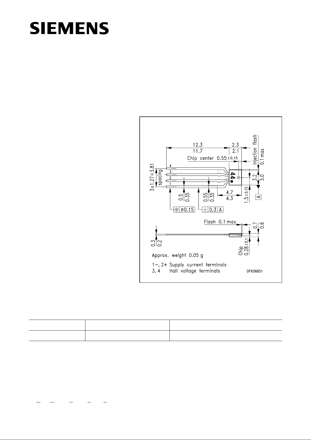
Dimensions in mm
Type Marking Ordering Code
KSY 44 44 Q62705-K265
The KSY 44 is a MOVPE
1)
Hall sensor in a mono-crystalline GaAs material, built into an
extremely flat plastic package (SOH). It is outstanding for a high magnetic sensitivity and
low temperature coefficients. The 0.35 × 0.35 mm
2
chip is mounted onto a non-magnetic
leadframe.
1) Metal Organic Vapour Phase Epitaxy
Semiconductor Group 1 1998-11-13
KSY 44
Maximum Ratings
Parameter Symbol Value Unit
Operating temperature
Storage temperature
Supply current
Thermal conductivity
soldered, in air
Characteristics (TA = 25 °C)
Nominal supply current
Open-circuit sensitivity
Open-circuit Hall voltage
I
= I1N, B = 0.1 T
1
Ohmic offset voltage
I
= I1N, B = 0 T
1
Linearity of Hall voltage
B = 0…0.5 T
B = 0…1.0 T
T
T
I
G
G
I
K
V
V
F
1
1N
A
stg
thA
thC
B0
20
R0
L
– 40…+ 175 °C
– 50…+ 180 °C
10 mA
≥ 1.5
≥ 2.2
mW/K
mW/K
7mA
150…265 V/AT
105…185 mV
≤ ± 15 mV
≤ ± 0.2
≤ ± 0.7
%
%
Input resistance
Output resistance
Temperature coefficient of the
B = 0 T R
B = 0 T R
TC
10
20
V20
open-circuit Hall voltage
I
= I1N, B = 0.1 T
1
Temperature coefficient of the internal
resistance,
B = 0 T
Temperature coefficient of ohmic offset
voltage,
Inductive zero component,
I
= I1N, B = 0 T
1
I
=0 A
1N
Switch-on drift of the ohmic offset
voltage
I
= I1N, B = 0 T
1
Noise figure
1) With time varying induction there exists an inductive voltage V
I
= 0):
1
= A2× dB/dt × 10-4 with V(V), A2 (cm2), B(T), t(s)
= V0(t = 1s) – V0(t = 0.1 s)
0
= V0(t = 3m) – V0(t = 1 s)
0
2)
3) ∆
current
V
ind
dV
V
TC
TC
2
dV
∆V
F
R10, R20
VR0
1)
2)
0
3)
0
600…900 Ω
1000…1500 Ω
∼ – 0.03 %/K
∼ + 0.3 %/K
∼ – 0.3 %/K
0.16 cm
≤ 0.3
≤ 0.1
2
mV
mV
∼ 10 dB
between the Hall voltage terminals (supply
ind
Semiconductor Group 2 1998-11-13
 Loading...