

Page 1

User Guide
i-3 V2 I/O Controller – Modbus
www.usa.siemens.com/i-3
3
Page 2

i-3® Control Technology V2
TM
DANGER
Hazardous voltage.
Will cause death or
serious injury.
Keep out.
Qualifi ed personnel only.
Disconnect and lock off all
power before working on
this equipment.
Safety Precautions
(a) Only qualified persons familiar with
the construction and operation of this
equipment should perform work described
in this set of instructions. Such work
should be performed only after reading
this complete set of instructions.
(b) Follow safety related work practices, as
described in NFPA 70E, part II, at all times.
(c) Hazardous voltages in electrical
equipment can cause severe personal
injury or death. Energizing this equipment
for the first time after initial installation
or maintenance is potentially dangerous.
Inspection and maintenance should be
performed on this equipment and
equipment to which power has been
cut off, disconnected, and electrically
isolated so that no accidental contact
can be made with energized parts.
(d) Some types of electrical equipment will
cause harmonics in the electrical system
which may result in overheating. Consider
this condition when determining this
equipment loading, as possible de-rating
of equipment may be necessary.
Important
The information contained herein is
general in nature and not intended for
specific application purposes. It does not
relieve the user of responsibility to use
sound practices in application, installation,
operation, and maintenance of the
equipment purchased. Siemens reserves
the right to make changes in the
specifications shown herein or to make
improvements at any time without notice
or obligations. Should a conflict arise
between the general information
contained in this publication and the
contents of drawings or supplementary
material or both, the latter shall
take precedence.
Qualified Person
For the purpose of this manual and
product labels, a qualified person is
one who is familiar with the installation,
construction, operation or maintenance
of the equipment and the hazards
involved. In addition, this person has
the following qualifications:
(a) is trained and authorized to
de-energize, clear, ground, and tag
circuits and equipment in accordance
with established safety practices.
(b) is trained in the correct care and
use of protective equipment such as
rubber gloves, hard hat, safety glasses
or face shields, flash clothing, etc.,
in accordance with established
safety practices.
(c) is trained in rendering first aid.
Signal Words
The signal words “Danger,” “Warning”
and “Caution” used in this manual
indicate the degree of hazard that
may be encountered by the user.
These words are defined as:
Danger - Indicates an imminently
hazardous situation which if not
avoided, will result in death or
serious injury.
Warning - Indicates a potentially
hazardous situation which, if not
avoided, could result in death or
serious injury.
Caution - Indicates a potentially
hazardous situation which, if not
avoided, may result in minor or
moderate injury.
Dangerous Procedures
In addition to other procedures
described in this manual as dangerous,
user personnel must adhere to the
following warnings:
(a) Danger! High Voltage. Qualified
personnel only. Lock off all power to
this equipment before working inside.
Always work on de-energized equipment.
Always de-energize equipment before
performing any tests, maintenance
or repair.
y
Warning! Alwa
(b)
on the interrupting device after the closing
mechanism(s) are discharged.
(c) Caution! Always let an interlock device
or safety mechanism perform its function
without forcing or defeating the device.
(d) Caution! Hydrocarbon spray
propellants and hydrocarbon compounds
will cause degradation of certain plastics.
Contact your local Siemens representative
before using these products to clean or
lubricate components during installation
or maintenance.
s perform maintenance
Page 3

TM
i-3® Control Technology V2
Chapter 1 Introduction 2
Over
Chapter 2 i-3 V2 I/O Controller 3
Introduction 3
I/O
Power Supply 7
Fuse Element 7
Switch Element 7
Ribbon Cables 7
USB to RS-485 Converter 7
Chapter 3 Control Input 8
Mounting Bracket 8
- Removing Communication Interface Door 8
- Removing Cover 8
Chapter 4 Control Inputs/Outputs 9
Introduction 9
Switc
Common Input Types 10
Changing Input Types 11
Input/Output Mapping 11
Chapter 5 Communication Protocols 12
Introduction 12
Configuring i-3 I/O Controller 12
- Using Panel Configurator Tool Software 12
- Using Modbus Communication 12
SIPOD Status 13
view 2
Board 4
I/O Contr
Connecting Controller to a Modbus System (PC or Building Automation System) 12
oller Box 8
h Inputs 9
Appendix 18-
s Tables 18-19
A Modbus Addr
B Circuits (SIPODs) Modbus Address Table 20-21
C Modbus Coils, Discrete Inputs, Input Registers and Holding Registers Address Tables 22-44
D Dimming Instructions 45-47
E USB to RS485 Converter Driver Software Installations Instructions 48-52
F Recommended Input Devices 53-72
G Common Networking setups 73-74
Customer Support Information 75
These instructions do not purport all details or variations in equipment, nor to provide for every possible contingency to be met in
connection with installation, operation or maintenance. Should further information be desired or should particular problems arise
which are not covered sufficiently for the purchaser’s purposes, the matter should be referred to the local Siemens sales office. The
contents of this instruction manual shall not become part of or modify any prior or existing agreement, commitment or relationship.
The sales contract contains the entire obligation of Siemens. The warranty contained in the contract between the parties is the sole
warranty of Siemens. Any statements contained herein do not create new warranties or modify the existing warranty.
es
1
Page 4
Chapter 1
Introduction
Overview
The purpose of this manual is to help users
develop safe and efficient procedures for
the installation, operation and maintenance
of the i-3 V2 I/O Modbus Controller.
The i-3 V2 I/O Controller is used to control
the operation of P1 Series with i-3 Control
Technology V2 Panel. The controller directs
SIPODs (Remotely Operated Contactors)
to switch ON/OFF. It also monitors the
contact status up to 42 branch circuits.
The i-3 V2 I/O Controller enables the P1
lighting panel to operate as a slave panel
to accept dry contact or wet digital inputs
and analog inputs or commands through
communications network by a Building
Automation System. It provides up to 20
two-wire dry or wet contact inputs and
two analog inputs which can be used to
control up to 42 outputs.
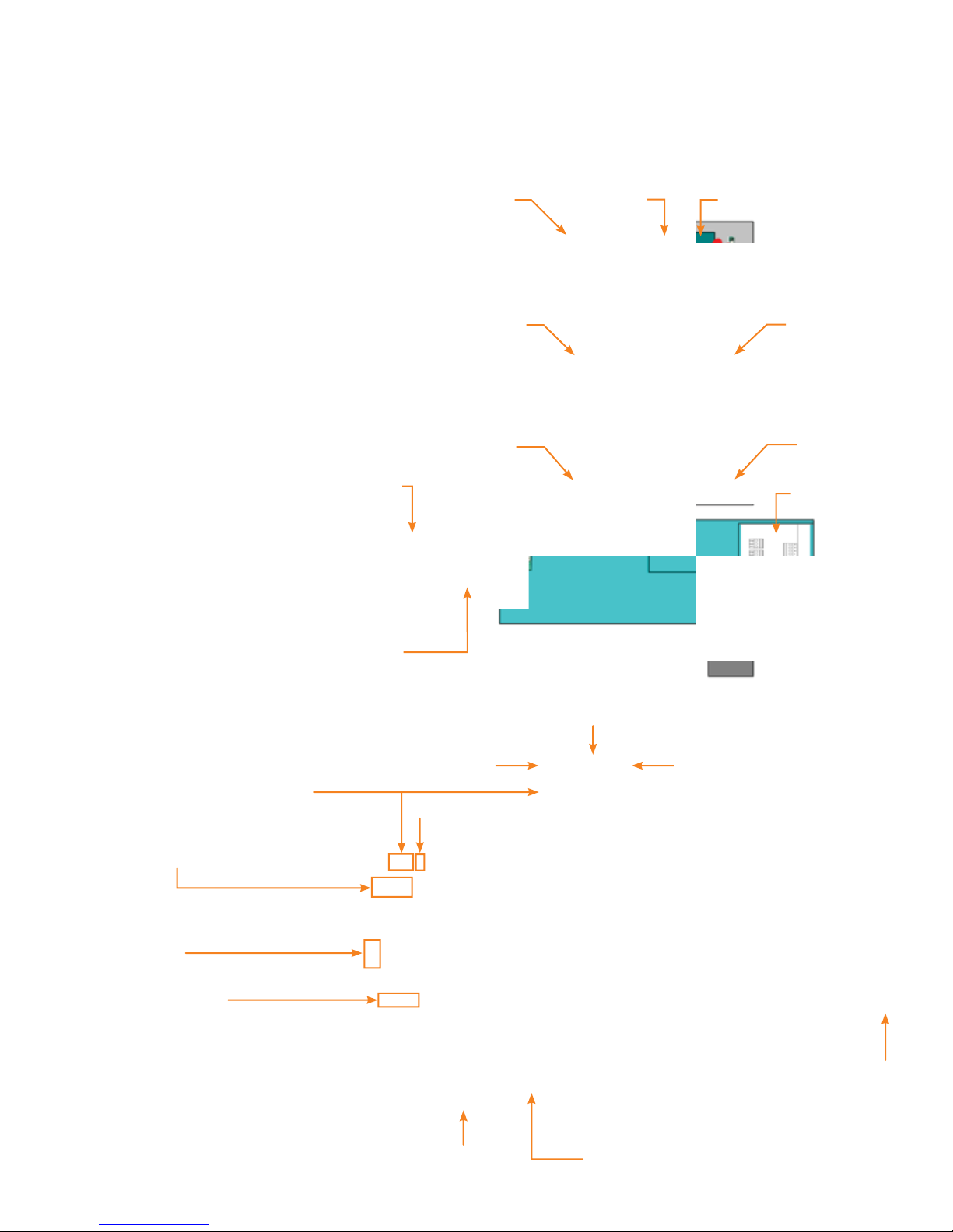
Figure 1.1
Single Slave Panel System Overview
PC or BAS
(Modbus
Interface)
RS485 to
RS232
converter
P1 Box
Data Rail
Ribbon
Cable
BQD SIPOD
Up to 21
Up to 21
I/O Board
Data Rail
Ribbon
Cable
Input
Terminals
Power
Supply
Front Panel Overview
Modbus
addressing switches
Connector
for Modbus
TCP/IP card
RS485 connections
Figure 1.2
i-3 Controller Front View
Three way switch
All ON-AUTO-ALL OFF
Normal
operation
All SIPOD ON
Reset
Fuse Power switch
All SIPOD OFF
Note: The switch must
be on the “A
position during
commissioning and
normal operation.
UTO”
Ribbon
cable
2
Page 5

Chapter 2
i-3 V2 I/O Controller
Introduction
The i-3 V2 I/O Controller consists of
I/O printed circuit board, power supply,
fuse, switch, ribbon cables, mounting
bracket and I/O controller housing. This
chapter will discuss these individual
components in detail.
Three way switch
All ON-AUTO-ALL OFF
Modbus
addressing
switches
Connector
for Modbus
TCP/IP card
Reset
I/O Board
The main component of i-3 V2 I/O
Controller is the I/O printed circuit
board. Figure 2.1 below shows main
parts and features of I/O Board.
Ribbon cables
connectors
Modbus
RS-485
connection
Figure 2.1
I/O Board Layout
Communications
interface section
Power supply
connector
Input /Output
wiring section
3
Page 6

Chapter 2
i-3 V2 I/O Controller
Switch input terminals (digital inputs)
(TB1 – TB2)
There are 20 switch input terminals
available to be used to connect to external
dry or wet contact switching devices. They
are capable of accepting up to 20 two-wire
dry or wet contact inputs. Two ten-pin
pluggable connectors will be used to
connect the input wires to external
devices. A six pin pluggable connector
(TB3) is used to connect the contacts
common to the board (if the six location
on the connector are not sufficient; the
commons may be jumped together
outside of the board and one common
wire can be brought into the board).
The recommended wire is 18 AWG
stranded copper.
Analog outputs (TB5)
Two 0-10 VDC, 100 mA each to control
0-10 V dimmable ballasts.
Analog inputs (TB6)
Two analog inputs to connect the 0-10 V
output from light sensors.
24 VDC (TB4)
Power supply for sensors (light, motion,
etc.) as well as for wet contacts.
Firmware upgrade connector
This connection is used for Factory Service
and is not available to users.
Ribbon cable connector
There are two ribbon cable connectors
on the I/O Board that interface with the
data rails located on each side of the
P1 Series Lighting Panel. For safety
purposes, ribbon cables have a key feature
that prevents them from being connected
in the wrong orientation. A white mark
indicates the location of pin 1. In addition,
the pin 1 wire is black. The black wire must
be connected to pin 1 of the connector
where it lines up with the white mark.
Modbus addressing switches
Used to set the controllers Modbus address
in hexadecimal format.
Connector for Modbus TCP/IP
optional card
The Modbus TCP/IP optional card (Figure
2.2) cable plugs into this connector.
Figure 2.2
Modbus optional TCP card
Figure 2.3
I/O Board Wiring Section
Analog outputs
(Center pin is common)
Analog inputs
(Center pin is common)
Digital inputs 1 -10
Dry or wet contacts
Digital inputs common
Firmware upgrade connector
(Siemens use only)
24 VDC (+)
24 VDC (–)
Digital inputs 11 -20
Dry or wet contacts
4
Page 7

Chapter 2
i-3 V2 I/O Controller
USB-RS485 converter kit
Part No. 5WG1715-8XY02
Phoenix connector
Part No. 1984028
FTD chip
Part No. USB-RS485-WE-1800-BT
Figure 2.4
USB Converter Kit
5
Page 8

Chapter 2
i-3 V2 I/O Controller
Three way switch
All ON-AUTO-ALL OFF
Modbus
RS-485
connection
Figure 2.5
Modbus board
Reset button
Three-way switch (Figure 2.6)
This switch is used to determine the
method operation of all SIPODs. It has 3
positions, “All ON”, “Auto” and “All OFF.”
• “All ON” – Forces all SIPOD contacts to
be closed. In this position, the I/O Boar
prevent SIPODs from accepting any
remote commands.
Figure 2.6
Three-way Switch
• “Auto” – SIPODs can be controlled
emotely by a Building Automation
r
System (BAS) or any Modbus master.
• “All OFF” – Forces all SIPOD contacts
o be opened. In this position, the I/O
t
d
Board prevents SIPODs from accepting
any remote commands.
All ON Auto
RS-485 terminals
The RS-485 terminals are used to connect
i-3 V2 I/O Controller to a Modbus Building
Automation System (BAS). They also
enable users to configure the i-3 V2 I/O
Controller and perform various diagnostic
tests with the configuration software.
Reset button
This button resets (reboots) the controller.
All OFF
6
Page 9

Chapter 2
i-3 V2 I/O Controller
Power supply
The power supply is mounted under the
I/O printed circuit board. It uses one of the
3-phase buses as the main power source.
The power supply provides power to the
controller and all its functions.
Fuse
The fuse protects the wire to the power
supply and I/O Board from short circuits.
This fuse is a 2 Amps class CC fuse rated
for 600Vac or less. Figure 2.7 shows
the fuse housing. To replace the fuse use
LittleFuse KLDR002 or equivalent.
Power switch
An ON/OFF switch controls power to the
i-3 V2 controller. Be sure to turn the power
switch OFF prior to removing the fuse from
the controller.
Ribbon cables
A pair of 26-wire ribbon cables connect
the I/O Board and the data rails. They
provide two-way data communication
between the I/O Board and SIPODs. They
also provide power and ground.
2A Fuse
Figure 2.7
Power Switch and Fuse Housing
On/Off Switch
Each ribbon cable has identical connectors
on each end. A “keying” feature reduces
the risk of installing the connectors in the
wrong orientation.
USB to RS-485 converter
A USB to RS-485 converter should be
purchased to allow communication
between the i-3 V2 I/O Controller and
a personal computer. FTD Chip part
# USB-RS485-WE-1800-BT is recommended,
however Siemens is not responsible for the
part’s functionality.
A converter may be purchased from
Siemens – Part No. 5WG1 715-8XY02.
Users may also build a converter; see
Figure 2.4.
Figure 2.8
Ribbon Cable
7
Page 10
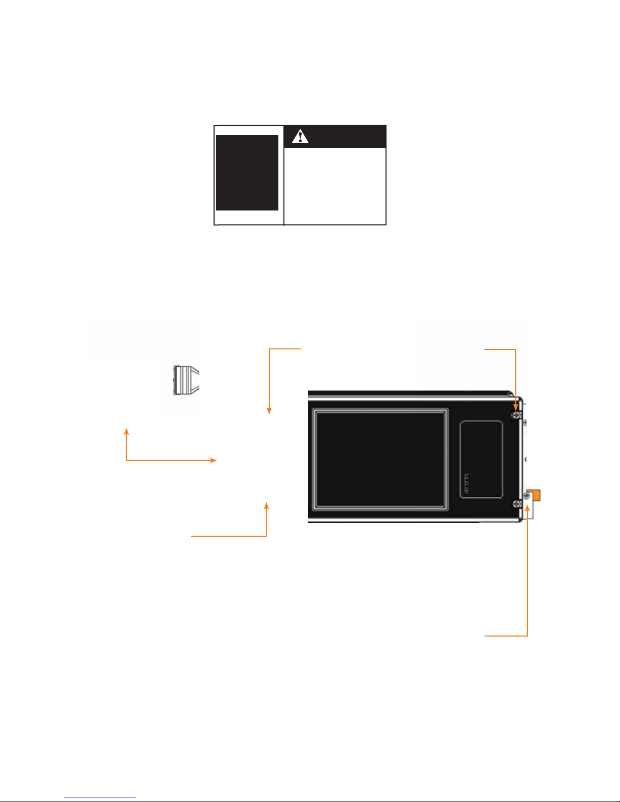
Chapter 3
Control Input
Mounting bracket
The mounting bracket is a “C” shape
steel plate that screws into the P1
panel mounting rails. This bracket holds
the controller.
I/O controller box
Removing the communication
interface door
The communication interface door
provides access to the communication
interface section without removing the
entire cover. Use the door handle shown
in Figure 3.1 to remove and install
the door.
DANGER
Hazardous voltage.
Will cause death or
serious injury.
Keep out.
Qualifi ed personnel only.
Disconnect and lock off all
power before working on
this equipment.
Door Handle
Removing the cover
Them I/O Controller cover must be removed
to access the input wiring section. Follow
the step-by-step instructions below to
remove the cover:
1. Disconnect and lock off all power
sources supplying this panel.
2. Remove P1 Panel trim and deadfront.
3. Remove the cover screws (4 total)
located as shown on Figure 3.1 to
remove the cover.
Cover screws (4)
“C” shape
mounting bracket
Communications
interface door
(shaded )
Figure 3.1
I/0 Controller Communication Interface Door
Controller
mounting screws (4)
8
Page 11

Chapter 4
Control Inputs/Outputs
Introduction
i-3 V2 I/O Controller provides a set of control
input terminals for wiring devices, such as
wall switches, photocells or occupancy
sensors. These terminals are located in the
input wiring section of the I/O printed
circuit board. There are two types of inputs
provided by these terminals:
• Switch inputs – The i-3 V2 I/O Contr
provides up to 20 input connections for
dry or wet (24 VDC) contacts (such as
wall switches, occupancy sensors, etc).
These contact inputs are capable of
acting either independently or in pairs
to turn ON and OFF. The controller can
accept up to 10 three-wire inputs or any
combination of two- and three-wire
inputs until its capacity is reached.
• Analog I/O – i-3 V2 I/O Contr
provides two analog input and two
analog output connections to control
0-10V dimming ballast.
There are two Analog Inputs (at TB6 on the
I/O Board) and two Analog Outputs (at TB5).
The Analog Inputs can be used to read any
0 to 10 Volt input value, and the Analog
Outputs can be used to drive out 0 to 10
volts ballast at a maximum of 100 mA each.
In a practical sense, this means that each
Analog Output can drive approximately 50
typical dimming ballasts (assuming each
ballast uses 2 mA – check your ballast
documentation for an actual determination).
Input / output connectors
oller
oller
The Analog Inputs can be used in any
situation where digital inputs are used.
They are specified by using input numbers
33 and 34, but whether they are “ON” or
“OFF” is more complex. For each analog
input, registers 20 and 21 give the input
value in the range 0-4095. Registers 36
and 37 specify values to be compared
to the Analog Inputs and comparison
operations, to determine whether the
Analog Input is ON or OFF.
Register 36 is the Compare definition for
Analog Input 1 (input number 33), and
contains the comparison value in the
bottom 12 bits (least significant, bits
0-11, range 0-4095). The high-order bit
(bit 15) in that register stands for “equal”
comparison, bit 14 stands for “less,” and bit
13 stands for “greater.” These three bits may
be combined to make “less or equal” or
“greater or equal” or “always ON” (all three
bits on). If all three bits are off, then the
Analog Input is never ON. Register 37
controls the comparison operation for
Analog Input 2 (input number 34).
Controlling the Analog Outputs: Registers
38 and 39 give the actual, read only values
of the Analog Outputs 1 and 2. Like all
Analog values, they are a number in the
range 0 to 4095, corresponding to 0 to 10
Volts. (NOTE: The actual output may be
limited by the circuitry to approximately
9.2 Volts.)
Registers 22 and 23 are for specifying
Analog Output 1 Set value and Analog
Output 2 Set value. These Set values are
intended to be used to drive the Analog
Outputs. However, whether these Set
values are used by the Analog Outputs
depends on the Analog Output Feed
registers, 32 and 33.
Each Analog Output’s actual output value
can be tied to an Analog Input or to register
22 or 23, but not both. The Analog Output
Feed registers determine this tie-in. Register
32 (Analog Output 1 Feed) contains the
number of the Input to be tied to the
Analog Output. This number is from 0 to
44, where 0 is “no connection” and 1-20
are digital inputs, while numbers of 33 and
34 are analog inputs 1 and 2. These two
analog inputs act as a digital inputs based
on the Analog compare register values.
Numbers 35 and 36 specify the analog
inputs and the feed is through the direct
values of the analog inputs. Numbers 37
and 38 specify the analog inputs and the
feed is through the difference of the Max
Voltage (4095) and the direct values of
the inputs.
Numbers 39 and 40 do not represent an
actual input, but instead ties this Analog
Output to register 22 or 23, respectively.
Register 33 is for specifying the Analog
Output 2 Feed. Numbers 42 and 42 specify
the use of the analog gain table. Numbers
43 and 44 specify the use of the PID loop
function with values E0 and E1 respectively.
Common
Figure 4-1
Input / Output Connectors
Digital inputs Analog I/0
24 VDC
9
Page 12

Chapter 4
Control Inputs/Outputs
The diagram below illustrates the position of these input terminals in
i-3 V2 controller I/O board.
Analog outputs
Analog inputs
Digital inputs
Digital inputs
common
TB5
TB6
TB1
TB3
TB4
TB2
24 VDC
Digital inputs
Figure 4-2
Input Terminals in the Input Wiring Section
Common input types
Table 4-1 lists the typical input types supported by i-3 Control Technology V2 system.
Input Type Description Comments
0 Digital input maintain toggle switch (2-wire) If the value changes, then invert the state
1 Digit
2 Digital input maintain normally on switch (2-wire)
3 Digital input maintain normally on switch (2-wire) – blinking
4 Digital input maintain normally off switch (2-wire)
5 Digital input maintain normally off switch (2-wire) – blinking
6 Digital input momentary toggle switch (2-wire)
7 Digital input momentary toggle switch (2-wire) – blinking
8 Digital input momentary normally on switch (2-wire)
9 Digital input momentary normally off switch (2-wire)
10 Digital input dual-momentary switch (3-wire)
11 Digital input dual-momentary switch (3-wire) – blinking
Table 4-1
Common Input Types
10
al input maintain toggle switch (2-wire) – blinking if the value changes, then invert the state
Page 13

Chapter 4
Control Inputs/Outputs
Changing input types
All input types can be changed using
the Modbus communication protocol.
Refer to Modbus Map on page 14 for
more information.
Input/output mapping
Setting input/output mapping can
be accomplished using Modbus
communication protocol or the
configuration software.
Any given input to the I/O Board may be
connected to one output or to an output
group or zone (which is more than one
output). Refer to Modbus Map table in
Chapter 5 –Communication Protocols
under “Configuring i-3 V2 I/O Controller”
section for more information.
11
Page 14

Chapter 5
Communication Protocol
Introduction
The i-3 V2 I/O Controller provides
Modbus as the standard communication
protocol. A personal computer or Building
Automation System may be connected to
i-3 V2 I/O Controller using a twisted pair
serial cable wired to RS-485 terminal
located in the communication interface
section of I/O Board.
The i-3 V2 I/O Controller will act as a
Modbus Slave using Modbus RTU or
Modbus TCP/IP (optional) slave protocol
when interfacing with Building
Automation System. Modbus master
devices connected to the controller
can access (read) the data, making
configuration changes and initiating
control actions.
Connecting the controller to a
Modbus System (PC or Building
Automation) system
A twisted pair serial cable is used to
connect the i-3 V2 I/O Controller to a
personal computer or Building Automation
System. RS-485 to RS- 232 conversion
cable is required to connect to a personal
computer. This cable is connected to the
RS-485 terminal which is located in
the I/O Board communication interface
section as shown in Figure 5.1.
The RS-485 terminal is accessible through
Communication Interface Door without
removing the panel deadfront. See Figure
3.1 on page 8.
Configuring i-3 V2 I/O Controller
There are two methods of configuring
i-3 V2 I/O Controller: using The Panel
Configurator Software or Modbus
communications.
1. Using the i-3 V2 I/O Configurator
Software
Refer to “i-3 V2 I/O Configurator
Software Tool” section for instructions
on how to download this program from
our Web site.
2. Using Modbus Communication
Assigning a Modbus address
By default, i-3 V2 I/O Controller device
address is assigned as 126. If multiple
i-3 V2 I/O Controllers or other Modbus
devices are present on the same line,
each device must be assigned a unique
device address.
The Modbus address is programmed
with rotary switches located on the
electronic board.
See Appendix A – Modbus Address
Table for rotary switch settings.
Changing input types
To change input types, follow the steps:
1. Use either function code 6, preset
single register or 16: preset multiple
registers.
2. The register address for input types
ranges from 1792 (for input terminal 1)
to 1811 (for input terminal 20).
3. Assign the desired input type value,
which can be found in the Modbus Map
Table on page 10. For example, input
type “3” is digital input maintain
normally ON switch (2-wire).
RS-485
Terminal
Figure 5.1
i-3 I/O Controller Communication Interface
12
Page 15

Chapter 5
Communication Protocols
Creating output groups
An output group consists of a set of
SIPODs. To create an output group, follow
these steps:
1. Use either function code 6: preset single
register or 16: preset multiple registers.
2. The register addresses for output group
definition ranges from 256 (for output
group definition 1) to 380 (for output
group definition 125).
3. Assign the register value to create as
many output groups as desired. Note:
Each register is made up of two bytes:
the first byte represents the output
group number and the second byte is
the SIPOD number. For example, if the
register contains 0x0402, then the
output group is 4 (0-relative numbering)
and the SIPOD is 2. There can be
duplicate output groups and/or SIPODs
within the table. This means an output
group can contain more than one SIPOD,
and a SIPOD can be in more than one
output group.
Mapping input-to-output
By default, the factory assembled i-3
V2 Controller input-to-output mapping
is not set. Input-to-Output mapping can
be redefined as desired to meet the project
specification. To map input to output,
follow these steps:
1. Use either function code 6: preset single
register or 16: preset multiple registers.
2. Register address for input-to-output map
starts from 2048 for input terminal 1 to
2067 for input terminal 32.
3. Assign the register value for the desired
input maps. Note: Each entry (register)
in the table has two parts: a high order
byte that is either 0 (for an output
mapping) or 0x80 (for an output group
mapping), and a low-order byte that
specifies either an output (SIPOD)
number or an output group number.
The table is indexed by input number.
For example, if the fifth entry (register)
in the table is 0x0001, then input
number 5 is mapped to SIPOD 1. If the
tenth entry (register) is 0x8004, then
input number 10 is mapped to output
number 4.
Refer to Modbus Map table on page 14
for additional information.
Other configuration functions
Other functions, such as reading SIPOD
status, reading input status, setting up
SIPOD parameter, etc., are listed in the
Modbus Map table on page 14.
13
Page 16

Chapter 5
Communication Protocols
Modbus map (See Appendix C)
This section describes the Modbus
communication protocol employed by the
i-3 V2 I/O Controller in a Modbus network.
Please contact Technical Support at
1-800-333-7421 to obtain the most
current Modbus Map.
SIPOD Status
The first (high-order) byte of the SIPOD
Status Word contains:
+---------------------------------------------------+
| P | R | D | O | S | S | | |
| O | S | E | V | P | P | | || Control byte
| D | T | F | F | 1 | 2 | | |
+--------------------------------------------------+
SIPOD – SIPOD initiated message – set
when the message originates in the SIPOD
rather than the I/O Board.
RST – Reset flag – sent from the SIPOD
to the I/O Board in the first message after
a system reset.
DEF/FIN – Default/Finishing flag
This flag has two meanings – one if the
message originates in the SIPOD, and
another if the message originates in the
I/O Board. In a SIPOD message, it means (if
on) that the default values of parameters
have not yet been set – in particular, no
“SetParameter” message has been received
from the IO Board since the most recent
SIPOD reset.
In messages originating in the I/O Board,
the FIN flag indicates that no more data
will be sent to the SIPOD. It also indicates
that no more data will be accepted. No
data may be sent in a packet which has the
FIN flag set. The FIN flag is not currently
used, and is intended for situations where
there are multiple packets sent from the I/O
Board – not for single messages.
OVF – Command overflow flag
This flag indicates that at least one
command previously sent to the SIPOD was
ignored because there was no room
in the task queue. This means that
commands are being sent too quickly
for the SIPOD to handle them.
SP1 – Status of Pole 1
This is equal to 1 if the first pole is closed.
SP2 – Status of Pole 2 (for 2-pole PODs)
This is equal to q if the second pole is
closed.
The second (low-order) byte of the
SIPOD Status Word contains:
• Bit 7 (left-most bit) – Open/Closed flag
ON = Closed;
OFF = Open.
• Bit 6 – OIP – Open in process flag
• Bit 5 – CIP – Close in process flag
• Bit 4 – FAIL – Failure flag (failed to open
close)
or
•
Bit 3 – NAK flag (a previous message
was g
• Bit 2 – MxO – Maximum Opens per
minute
• Bit 1 – MxC – Maximum Closes per
minute
• Bit 0 – SQE – Sequence Error flag (a
pr
The Open/Closed flag is set based on the
Auxiliary Detector in the SIPOD. This is a
contact switch that mimics the operation
of the power contacts.
Note that the FAIL, NAK, and SQE flags
are sent only once, and then cleared. All
three of these flags mean that there was
a problem since the last time a status was
sent to the I/O Board – not necessarily
related to the previous message from the
I/O Board. For example, if the I/O Board
requests an Open, then a Close, then sends
GetStatus and the status contains
a FAIL flag, then either the Open or the
Close failed (or both), but the I/O Board
cannot determine which operation failed.
Timed inputs
Each register represents a 16-bit signed
value (-32766 to +32767), which gives
the number of minutes to time an input
when it is switched ON. The default is 0,
meaning “do not time this input”. The
maximum value is 32767 (about
22.75 days).
After this time, the input will be turned
“OFF” logically – that is, the switch may
be physically in the ON position, but any
SIPODs mapped to it will be turned off.
arbled)
reached
reached
evious message was out-of sequence)
NOTE: There is a built-in delay of up to
one minute, so setting this time to 1 will
result in the input turning “OFF” after a
minimum of one minute and maximum
of two minutes.
Putting 0 in this register means there is no
timing: that is, the switch is ON indefinitely
until operated OFF.
Timed SIPOD overrides
Each register represents a 16-bit signed
value (-32766 to +32767), which gives
the number of minutes to time a SIPOD
override. The default is 0, meaning “ there
is no override.” The maximum time is +
or - 32767 (about 22.75 days). A positive
value will turn the SIPOD ON for that
amount of time. A negative value means
the SIPOD will be turned OFF for that
amount of time.
For example, a value of +15 will turn the
SIPOD ON for 15 minutes. A value of -20
will turn the SIPOD OFF for 20 minutes. So
the absolute value of the register indicates
the time, and the sign of the register indicates ON or OFF.
After this time, the override will be
disabled logically. The SIPOD will return
to whatever state (ON/OFF) it would be
in if the override had not happened.
Putting 0 in this register means the
override is disabled. In other words,
overrides are always time-limited.
If the registers are read, they return the
value of the time left in the override and
indicate by being negative or positive
whether the SIPOD is turned OFF or ON.
IOB control word
As a safety precaution, there is a password
value required in the high-order byte of the
IOB Control Word to enable use of
any of the control bits. This is to prevent
accidental activation of the control bits
it is not meant to prevent unauthorized
access. The password value is 0xA0
(hexadecimal A0, decimal 160).
Note that the IOB Control Word always
returns 0 (0x0000) when read.
Bit 0 -- if ON, clears all statistics of the
IO Board
14
Page 17

Chapter 5
Communication Protocols
Bit 1 -- if ON, run the IOB Diagnostics
routine
Bit 2 -- if ON, reset the IO Board
Bit 3 -- if ON, restore defaults to the
parameters of the IO Board (but not the
Modbus device address) as well as the
Date and Time.
Bit 4 -- if ON, restore defaults to the
Output Groups Table (i.e., no output
groups defined) and the Input-Output
Mapping Table (i.e., 1-to-1 mapping of
32 digital inputs to the first 32 outputs)
Bit 5 -- If ON, restore defaults to the Input
Types Table (i.e., all digital input types set
to 0) and to Inputs Force (i.e., turn off
all forcing). In addition, the states of all
inputs are initialized.
Bit 6 -- If ON, indicates the IO Board should
go into Program Upgrade mode – stopping
all activity except for receiving memory
updates (allows reading/writing of the IOB
Memory Access Table and writing register
115 – the IOB Control Word)
Bit 7 -- If ON, cancels the Program Upgrade
mode (IO Board goes back into normal
mode – all normal functions are enabled)
To activate one or more of these bits, you
must add the password value and write the
word. For example, if you wish to reset
the IO Board, you must write 0xA004
(hexadecimal A004).
Input forcing
Using a combination of the Inputs On/Off
(registers 18 and 19) and the Inputs Force
(registers 16 and 17), the user can force
the state of individual and multiple inputs
to be either On or Off. The Force All
On/Off switch on the IO Board still has
the highest priority of action, but Input
Forcing is second to that switch when it
comes to priority of action.
The state of an input (On or Off) can be
read or written in registers 18 and 19.
However, writing to an input state has
no effect unless the corresponding bit in
registers 16 or 17 is set to 1. Therefore,
registers 16 and 17 act as a mask of
registers that are being forced, and
registers 18 and 19 act as forced states or
actual states of inputs, depending on the
mask registers.
Note that when an input is being forced,
the actual state of the input has no effect
whatsoever, until the forcing is turned
OFF for that input. This may lead to some
confusion, i.e., someone trying to toggle a
light switch and seeing nothing happen to
the lights.
Panel configurator tool software
To obtain this software, please contact
Siemens at 800-427-2256. Software will
be available for download online.
Input Logics
Registers 3584 through 3603 specify an
optional logic operation for each Input.
Each register contains a 0 (“OR”), 1
(“AND”), 2 (“NAND”), or 3 (“XOR”) in the
first byte and an input number (1-20 for
digital inputs or 33 analog input 1 or 34
for analog input 3) in the second byte. A
value of 0 in a register means that there is
no Logic operation to be applied. A Logic
operation allows the user to relate two
different inputs to a POD with an AND,
OR, NAND, or XOR logical connection.
NOTE: A special situation can occur when
two inputs are linked to each other and
one has an “OR” operation and the other
has an “AND” operation. This could lead to
a race condition, causing the SIPODs to
clatter as they try to satisfy both conditions.
In order to prevent this, the software
will automatically give both Inputs the
same Logic operation whenever it detects
the condition. In the case or an XOR or a
NAND, just the opposite is true, in that if
both inputs point to each other and have
XOR or both have NAND, this creates a
race condition, so the system removes
the Logic operation
Communication loss
Placing a value in register 781 indicates how
long (in minutes) the I/O board should wait
to determine if communication is lost. The
15th bit in register 781 specifies what to do
when communication is lost. If the 15th bit
is set, all SIPODs will be turned ON. If the
15th bit is not set, all SIPODs will be turned
OFF. The user enters the value in the
remaining 15 bits. The maximum value is
10000 minutes, the minimum value is 1
minute. If the value is FFFF, the I/O board
does not check for communication loss.
SIPOD Delay
The user can specify the time (in
milliseconds) for SIPODs to be ON for
the commands SIPOD_CLOSE and
SIPOD_OPEN. The default its 0. The
maximum is 65536.
1.1. Analog Gain Tables
Register Function Value
Analog Gain Output Table
0x2000 Lighting level 1 setting 0 - 4095
0x2001 Lighting level 2 setting 0 - 4095
0x2002 Lighting level 3 setting 0 - 4095
0x2003 Lighting level 4 setting 0 – 4095
0x2004 Lighting level 5 setting 0 – 4095
0x2005 Lighting level 6 setting 0 – 4095
0x2006 Lighting level 7 setting 0 – 4095
0x2007 Lighting level 8 setting 0 - 4095
0x2008 Lighting level 9 setting 0 – 4095
0x2009 Lighting level 10 setting 0 – 4095
Table 5.1
Analog Gain Input Table
0x200A Threshold level 1 setting 0 – 4095
0x200B Threshold level 2 setting 0 – 4095
0x200C Threshold level 3 setting 0 – 4095
0x200D Threshold level 4 setting 0 – 4095
0x200E Threshold level 5 setting 0 – 4095
0x200F Threshold level 6 setting 0 – 4095
0x2010 Threshold level 7 setting 0 – 4095
0x2011 Threshold level 8 setting 0 – 4095
0x2012 Threshold level 9 setting 0 – 4095
0x2013 Threshold level 10 setting 0 - 4095
Table 5.2
Analog Active PID Settings
0x2014 Desired Lighting level
analog channel 1 0 – 4095
0x2015 Desired Lighting level
analog channel 2 0 - 4095
Table 5.3
15
Page 18

Chapter 5
Communication Protocols
Analog Gain
If the analog feedback data from the lighting sensor falls between 0 and threshold
setting 1, Programmable Ramp sets the
analog output to level 1.
If the analog input data from the lighting
sensor falls between threshold setting 1
and threshold setting 2, Programmable
Ramp sets the analog output to level 2.
If the analog input data from the lighting
sensor falls between threshold setting 2
and threshold setting 3, Programmable
Ramp sets the analog output to level
3, etc.
Saved Parameters
Certain parameters of the I/O Board are
saved to flash memory, so they can be
recovered after the system is reset and/or
after the power is turned OFF and back ON.
These are the registers that are saved to
Flash memory:
Register Description
32-39 Analog configuration
106 (Number of flash writes)
107-110
116 (Analog Input 1 Hysteresis)
117 (Analog Input 1 Epsilon)
120 (Modbus device address)
121-123
256-380 (Output Group Definitions)
768-779 (Default Parameters)
1792-1825 (Input Types Table)
2048-2081
2816-2836 (POD Types Table)
3072-3103 (Input Timing Table)
3328-3369
3584-3617 (Input Logics Table)
8192-8213 (Analog Gain Tables)
Table 5.4
(Analog Output Correction
factors)
(RS-485 baud rate, parity,
and stop bits)
(Input-Output Mapping
Table)
(POD Override Timing
Table)
16
Page 19

Appendix A
Modbus Address Table
Appendix B
Circuits (SIPODs) Modbus Address Table
Appendix C
Modbus Coils, Discrete Inputs, Input Registers and Holding Registers
Address Tables
Appendix D
Dimming Instructions
Appendix E
USB to RS485 Converter Driver Software Installations Instructions
Appendix F
Recommended input devices
Appendix G
Common Networking setups
17
Page 20

Appendix A
Modbus Address Tables
Modbus
Address
1 0 1
2 0 2
3 0 3
4 0 4
5 0 5
6 0 6
7 0 7
8 0 8
9 0 9
10 0 a
11 0 b
12 0 c
13 0 d
14 0 e
15 0 f
16 1 0
17 1 1
18 1 2
19 1 3
20 1 4
21 1 5
22 1 6
23 1 7
24 1 8
25 1 9
26 1 a
27 1 b
28 1 c
29 1 d
30 1 e
31 1 f
32 2 0
33 2 1
34 2 2
35 2 3
36 2 4
37 2 5
38 2 6
39 2 7
40 2 8
41 2 9
42 2 a
43 2 b
44 2 c
45 2 d
46 2 e
47 2 f
48 3 0
49 3 1
50 3 2
Dip Switch 1
(S4)
Dip Switch 2
(S5)
Modbus
Address
51 3 3
52 3 4
53 3 5
54 3 6
55 3 7
56 3 8
57 3 9
58 3 a
59 3 b
60 3 c
61 3 d
62 3 e
63 3 f
64 4 0
65 4 1
66 4 2
67 4 3
68 4 4
69 4 5
70 4 6
71 4 7
72 4 8
73 4 9
74 4 a
75 4 b
76 4 c
77 4 d
78 4 e
79 4 f
80 5 0
81 5 1
82 5 2
83 5 3
84 5 4
85 5 5
86 5 6
87 5 7
88 5 8
89 5 9
90 5 a
91 5 b
92 5 c
93 5 d
94 5 e
95 5 f
96 6 0
97 6 1
98 6 2
99 6 3
100 6 4
Dip Switch 1
(S4)
Dip Switch 2
(S5)
Modbus
Address
101 6 5
102 6 6
103 6 7
104 6 8
105 6 9
106 6 a
107 6 b
108 6 c
109 6 d
110 6 e
111 6 f
112 7 0
113 7 1
114 7 2
115 7 3
116 7 4
117 7 5
118 7 6
119 7 7
120 7 8
121 7 9
122 7 a
123 7 b
124 7 c
125 7 d
126 7 e
127 7 f
128 8 0
129 8 1
130 8 2
131 8 3
132 8 4
133 8 5
134 8 6
135 8 7
136 8 8
137 8 9
138 8 a
139 8 b
140 8 c
141 8 d
142 8 e
143 8 f
144 9 0
145 9 1
146 9 2
147 9 3
148 9 4
149 9 5
150 9 6
Dip Switch 1
(S4)
Dip Switch 2
(S5)
18
Page 21

Appendix A
Modbus Address Tables
Modbus
Address
151 9 7
152 9 8
153 9 9
154 9 a
155 9 b
156 9 c
157 9 d
158 9 e
159 9 f
160 a 0
161 a 1
162 a 2
163 a 3
164 a 4
165 a 5
166 a 6
167 a 7
168 a 8
169 a 9
170 a a
171 a b
172 a c
173 a d
174 a e
175 a f
176 b 0
177 b 1
178 b 2
179 b 3
180 b 4
181 b 5
182 b 6
183 b 7
184 b 8
185 b 9
186 b a
187 b b
188 b c
189 b d
190 b e
191 b f
192 c 0
193 c 1
194 c 2
195 c 3
196 c 4
197 c 5
198 c 6
199 c 7
200 c 8
Dip Switch 1
(S4)
Dip Switch 2
(S5)
Modbus
Address
201 c 9
202 c a
203 c b
204 c c
205 c d
206 c e
207 c f
208 d 0
209 d 1
210 d 2
211 d 3
212 d 4
213 d 5
214 d 6
215 d 7
216 d 8
217 d 9
218 d a
219 d b
220 d c
221 d d
222 d e
223 d f
224 e 0
225 e 1
226 e 2
227 e 3
228 e 4
229 e 5
230 e 6
231 e 7
232 e 8
233 e 9
234 e a
235 e b
236 e c
237 e d
238 e e
239 e f
240 f 0
241 f 1
242 f 2
243 f 3
244 f 4
245 f 5
246 f 6
247 f 7
Dip Switch 1
(S4)
Dip Switch 2
(S5)
19
Page 22

Appendix B
Circuits (SIPODs) Modbus Address Table
1-3® Control Technology V2 – Circuit Numbering, Modbus Addressing
Top feed – 42 circuits – vertical numbering
Circuit No. Modbus Addr Circuit No. Modbus Addr
1 02221
2 12322
3 22423
4 32524
5 42625
6 52726
7 62827
8 72928
9 83029
10 9 31 30
11 10 32 31
12 11 33 32
13 12 34 33
14 13 35 34
15 14 36 35
16 15 37 36
17 16 38 37
18 17 39 38
19 18 40 39
20 19 41 40
21 20 42 41
Top feed – 30 circuits – vertical numbering
Circuit No. Modbus Addr Circuit No. Modbus Addr
1
2
3
4
5
6
7
8
9
10
11
12
13
14
15
0
1
2
3
4
5
6
7
8
9
10
11
12
13
14
16
17
18
19
20
21
22
23
24
25
26
27
28
29
30
21
22
23
24
25
26
27
28
29
30
31
32
33
34
35
Bottom feed – 42 circuits – vertical numbering
Circuit No. Modbus Addr Circuit No. Modbus Addr
1
2
3
4
5
6
7
8
9
10
11
12
13
14
15
16
17
18
19
20
21
Bottom feed – 30 circuits – vertical numbering
Circuit No. Modbus Addr Circuit No. Modbus Addr
1
2
3
4
5
6
7
8
9
10
11
12
13
14
15
41
40
39
38
37
36
35
34
33
32
31
30
29
28
27
26
25
24
23
22
21
35
34
33
32
31
30
29
28
27
26
25
24
23
22
21
22
23
24
25
26
27
28
29
30
31
32
33
34
35
36
37
38
39
40
41
42
16
17
18
19
20
21
22
23
24
25
26
27
28
29
30
20
19
18
17
16
15
14
13
12
11
10
9
8
7
6
5
4
3
2
1
0
14
13
12
11
10
9
8
7
6
5
4
3
2
1
0
Top feed – 18 circuits – vertical numbering
Circuit No. Modbus Addr Circuit No. Modbus Addr
1
2
3
4
5
6
7
8
9
20
0
1
2
3
4
5
6
7
8
16
17
18
19
20
21
22
23
24
21
22
23
24
25
26
27
28
29
Bottom feed – 18 circuits – vertical numbering
Circuit No. Modbus Addr Circuit No. Modbus Addr
1
2
3
4
5
6
7
8
9
29
28
27
26
25
24
23
22
21
10
11
12
13
14
15
16
17
18
8
7
6
5
4
3
2
1
0
Page 23

Appendix B
Circuits (SIPODs) Modbus Address Table
1-3® Control Technology V2 – Circuit Numbering, Modbus Addressing
Top feed – 42 circuits – horizontal numbering
Circuit No. Modbus Addr Circuit No. Modbus Addr
1
3
5
7
9
11
13
15
17
19
21
23
25
27
29
31
33
35
37
39
41
Top feed – 30 circuits – horizontal numbering
Circuit No. Modbus Addr Circuit No. Modbus Addr
1
3
5
7
9
11
13
15
17
19
21
23
25
27
29
0
1
2
3
4
5
6
7
8
9
10
11
12
13
14
15
16
17
18
19
20
0
1
2
3
4
5
6
7
8
9
10
11
12
13
14
2
4
6
8
10
12
14
16
18
20
22
24
26
28
30
32
34
36
38
40
42
2
4
6
8
10
12
14
16
18
20
22
24
26
28
30
21
22
23
24
25
26
27
28
29
30
31
32
33
34
35
36
37
38
39
40
41
21
22
23
24
25
26
27
28
29
30
31
32
33
34
35
Bottom feed – 42 circuits – horizontal numbering
Circuit No. Modbus Addr Circuit No. Modbus Addr
1
3
5
7
9
11
13
15
17
19
21
23
25
27
29
31
33
35
37
39
41
Bottom feed – 30 circuits – horizontal numbering
Circuit No. Modbus Addr Circuit No. Modbus Addr
1
3
5
7
9
11
13
15
17
19
21
23
25
27
29
41
40
39
38
37
36
35
34
33
32
31
30
29
28
27
26
25
24
23
22
21
35
34
33
32
31
30
29
28
27
26
25
24
23
22
21
2
4
6
8
10
12
14
16
18
20
22
24
26
28
30
32
34
36
38
40
42
2
4
6
8
10
12
14
16
18
20
22
24
26
28
30
20
19
18
17
16
15
14
13
12
11
10
9
8
7
6
5
4
3
2
1
0
14
13
12
11
10
9
8
7
6
5
4
3
2
1
0
Top feed – 18 circuits – horizontal numbering
Circuit No. Modbus Addr Circuit No. Modbus Addr
1
3
5
7
9
11
13
15
17
0
1
2
3
4
5
6
7
8
2
4
6
8
10
12
14
16
18
21
22
23
24
25
26
27
28
29
Bottom feed – 18 circuits – horizontal numbering
Circuit No. Modbus Addr Circuit No. Modbus Addr
1
3
5
7
9
11
13
15
17
29
28
27
26
25
24
23
22
21
2
4
6
8
10
12
14
16
18
8
7
6
5
4
3
2
1
0
21
Page 24

Appendix C
Modbus Coils, Discrete Inputs, Input Registers & Holding Registers Address Tables
Coils
Function Code
1 (Read Only) 0 00001 0 / 1 SIPOD 1 Open (0)/Close (1)
5 & 15 (Write Only) * 1 00002 0 / 1 SIPOD 2 Open (0)/Close (1)
Modbus
Base 0 address
2 00003 0 / 1 SIPOD 3 Open (0)/Close (1)
3 00004 0 / 1 SIPOD 4 Open (0)/Close (1)
4 00005 0 / 1 SIPOD 5 Open (0)/Close (1)
5 00006 0 / 1 SIPOD 6 Open (0)/Close (1)
6 00007 0 / 1 SIPOD 7 Open (0)/Close (1)
7 00008 0 / 1 SIPOD 8 Open (0)/Close (1)
8 00009 0 / 1 SIPOD 9 Open (0)/Close (1)
9 00010 0 / 1 SIPOD 10 Open (0)/Close (1)
10 00011 0 / 1 SIPOD 11 Open (0)/Close (1)
11 00012 0 / 1 SIPOD 12 Open (0)/Close (1)
12 00013 0 / 1 SIPOD 13 Open (0)/Close (1)
13 00014 0 / 1 SIPOD 14 Open (0)/Close (1)
14 00015 0 / 1 SIPOD 15 Open (0)/Close (1)
15 00016 0 / 1 SIPOD 16 Open (0)/Close (1)
16 00017 0 / 1 SIPOD 17 Open (0)/Close (1)
17 00018 0 / 1 SIPOD 18 Open (0)/Close (1)
18 00019 0 / 1 SIPOD 19 Open (0)/Close (1)
19 00020 0 / 1 SIPOD 20 Open (0)/Close (1)
20 00021 0 / 1 SIPOD 21 Open (0)/Close (1)
21 00022 0 / 1 SIPOD 22 Open (0)/Close (1)
22 00023 0 / 1 SIPOD 23 Open (0)/Close (1)
23 00024 0 / 1 SIPOD 24 Open (0)/Close (1)
24 00025 0 / 1 SIPOD 25 Open (0)/Close (1)
25 00026 0 / 1 SIPOD 26 Open (0)/Close (1)
26 00027 0 / 1 SIPOD 27 Open (0)/Close (1)
27 00028 0 / 1 SIPOD 28 Open (0)/Close (1)
28 00029 0 / 1 SIPOD 29 Open (0)/Close (1)
29 00030 0 / 1 SIPOD 30 Open (0)/Close (1)
30 00031 0 / 1 SIPOD 31 Open (0)/Close (1)
31 00032 0 / 1 SIPOD 32 Open (0)/Close (1)
32 00033 0 / 1 SIPOD 33 Open (0)/Close (1)
33 00034 0 / 1 SIPOD 34 Open (0)/Close (1)
34 00035 0 / 1 SIPOD 35 Open (0)/Close (1)
35 00036 0 / 1 SIPOD 36 Open (0)/Close (1)
36 00037 0 / 1 SIPOD 37 Open (0)/Close (1)
37 00038 0 / 1 SIPOD 38 Open (0)/Close (1)
38 00039 0 / 1 SIPOD 39 Open (0)/Close (1)
39 00040 0 / 1 SIPOD 40 Open (0)/Close (1)
40 00041 0 / 1 SIPOD 41 Open (0)/Close (1)
41 00042 0 / 1 SIPOD 42 Open (0)/Close (1)
42-63 ... Reserved
64 00065 0 / 1 Output Group (Zone) 1, Open (0) /Close (1)
65 00066 0 / 1 Output Group (Zone) 2, Open (0) /Close (1)
66 00067 0 / 1 Output Group (Zone) 3, Open (0) /Close (1)
67 00068 0 / 1 Output Group (Zone) 4, Open (0) /Close (1)
68 00069 0 / 1 Output Group (Zone) 5, Open (0) /Close (1)
69 00070 0 / 1 Output Group (Zone) 6, Open (0) /Close (1)
70 00071 0 / 1 Output Group (Zone) 7, Open (0) /Close (1)
71 00072 0 / 1 Output Group (Zone) 8, Open (0) /Close (1)
72 00073 0 / 1 Output Group (Zone) 9, Open (0) /Close (1)
73 00074 0 / 1 Output Group (Zone) 10, Open (0)/Close (1)
74 00075 0 / 1 Output Group (Zone) 11, Open (0)/Close (1)
75 00076 0 / 1 Output Group (Zone) 12, Open (0)/Close (1)
76 00077 0 / 1 Output Group (Zone) 13, Open (0)/Close (1)
Modbus
5 digit address
Value
(Read/Write*) Description
22
Page 25

Appendix C
Modbus Coils, Discrete Inputs, Input Registers & Holding Registers Address Tables
Coils
Function code
Modbus
base 0 address
77 00078 0 / 1 Output Group (Zone) 14, Open (0)/Close (1)
78 00079 0 / 1 Output Group (Zone) 15, Open (0)/Close (1)
79 00080 0 / 1 Output Group (Zone) 16, Open (0)/Close (1)
80 00081 0 / 1 Output Group (Zone) 17, Open (0)/Close (1)
81 00082 0 / 1 Output Group (Zone) 18, Open (0)/Close (1)
82 00083 0 / 1 Output Group (Zone) 19, Open (0)/Close (1)
83 00084 0 / 1 Output Group (Zone) 20, Open (0)/Close (1)
84 00085 0 / 1 Output Group (Zone) 21, Open (0)/Close (1)
85 00086 0 / 1 Output Group (Zone) 22, Open (0)/Close (1)
86 00087 0 / 1 Output Group (Zone) 23, Open (0)/Close (1)
87 00088 0 / 1 Output Group (Zone) 24, Open (0)/Close (1)
88 00089 0 / 1 Output Group (Zone) 25, Open (0)/Close (1)
89 00090 0 / 1 Output Group (Zone) 26, Open (0)/Close (1)
90 00091 0 / 1 Output Group (Zone) 27, Open (0)/Close (1)
91 00092 0 / 1 Output Group (Zone) 28, Open (0)/Close (1)
92 00093 0 / 1 Output Group (Zone) 29, Open (0)/Close (1)
93 00094 0 / 1 Output Group (Zone) 30, Open (0)/Close (1)
94 00095 0 / 1 Output Group (Zone) 31, Open (0)/Close (1)
95 00096 0 / 1 Output Group (Zone) 32, Open (0)/Close (1)
96 00097 0 / 1 Output Group (Zone) 33, Open (0)/Close (1)
97 00098 0 / 1 Output Group (Zone) 34, Open (0)/Close (1)
98 00099 0 / 1 Output Group (Zone) 35, Open (0)/Close (1)
99 00100 0 / 1 Output Group (Zone) 36, Open (0)/Close (1)
100 00101 0 / 1 Output Group (Zone) 37, Open (0)/Close (1)
101 00102 0 / 1 Output Group (Zone) 38, Open (0)/Close (1)
102 00103 0 / 1 Output Group (Zone) 39, Open (0)/Close (1)
103 00104 0 / 1 Output Group (Zone) 40, Open (0)/Close (1)
104 00105 0 / 1 Output Group (Zone) 41, Open (0)/Close (1)
105 00106 0 / 1 Output Group (Zone) 42, Open (0)/Close (1)
106 00107 0 / 1 Output Group (Zone) 43, Open (0)/Close (1)
107 00108 0 / 1 Output Group (Zone) 44, Open (0)/Close (1)
108 00109 0 / 1 Output Group (Zone) 45, Open (0)/Close (1)
109 00110 0 / 1 Output Group (Zone) 46, Open (0)/Close (1)
110 00111 0 / 1 Output Group (Zone) 47, Open (0)/Close (1)
111 00112 0 / 1 Output Group (Zone) 48, Open (0)/Close (1)
112 00113 0 / 1 Output Group (Zone) 49, Open (0)/Close (1)
113 00114 0 / 1 Output Group (Zone) 50, Open (0)/Close (1)
114 00115 0 / 1 Output Group (Zone) 51, Open (0)/Close (1)
115 00116 0 / 1 Output Group (Zone) 52, Open (0)/Close (1)
116 00117 0 / 1 Output Group (Zone) 53, Open (0)/Close (1)
117 00118 0 / 1 Output Group (Zone) 54, Open (0)/Close (1)
118 00119 0 / 1 Output Group (Zone) 55, Open (0)/Close (1)
119 00120 0 / 1 Output Group (Zone) 56, Open (0)/Close (1)
120 00121 0 / 1 Output Group (Zone) 57, Open (0)/Close (1)
121 00122 0 / 1 Output Group (Zone) 58, Open (0)/Close (1)
122 00123 0 / 1 Output Group (Zone) 59, Open (0)/Close (1)
123 00124 0 / 1 Output Group (Zone) 60, Open (0)/Close (1)
124 00125 0 / 1 Output Group (Zone) 61, Open (0)/Close (1)
125 00126 0 / 1 Output Group (Zone) 62, Open (0)/Close (1)
126 00127 0 / 1 Output Group (Zone) 63, Open (0)/Close (1)
Modbus
5 digit address
Value
(Read/Write*) Description
23
Page 26

Appendix C
Modbus Coils, Discrete Inputs, Input Registers & Holding Registers Address Tables
Discrete inputs
Function code
2 (Read Only) 0 10001 0 / 1 Digital Input 1 Off (0)/On (1)
Modbus
Base 0 address
1 10002 0 / 1 Digital Input 2 Off (0)/On (1)
2 10003 0 / 1 Digital Input 3 Off (0)/On (1)
3 10004 0 / 1 Digital Input 4 Off (0)/On (1)
4 10005 0 / 1 Digital Input 5 Off (0)/On (1)
5 10006 0 / 1 Digital Input 6 Off (0)/On (1)
6 10007 0 / 1 Digital Input 7 Off (0)/On (1)
7 10008 0 / 1 Digital Input 8 Off (0)/On (1)
8 10009 0 / 1 Digital Input 9 Off (0)/On (1)
9 10010 0 / 1 Digital Input 10 Off (0)/On (1)
10 10011 0 / 1 Digital Input 11 Off (0)/On (1)
11 10012 0 / 1 Digital Input 12 Off (0)/On (1)
12 10013 0 / 1 Digital Input 13 Off (0)/On (1)
13 10014 0 / 1 Digital Input 14 Off (0)/On (1)
14 10015 0 / 1 Digital Input 15 Off (0)/On (1)
15 10016 0 / 1 Digital Input 16 Off (0)/On (1)
16 10017 0 / 1 Digital Input 17 Off (0)/On (1)
17 10018 0 / 1 Digital Input 18 Off (0)/On (1)
18 10019 0 / 1 Digital Input 19 Off (0)/On (1)
19 10020 0 / 1 Digital Input 20 Off (0)/On (1)
20 10021 0 / 1 Digital Input 21 Off (0)/On (1)*
21 10022 0 / 1 Digital Input 22 Off (0)/On (1)*
22 10023 0 / 1 Digital Input 23 Off (0)/On (1)*
23 10024 0 / 1 Digital Input 24 Off (0)/On (1)*
24 10025 0 / 1 Digital Input 25 Off (0)/On (1)*
25 10026 0 / 1 Digital Input 26 Off (0)/On (1)*
26 10027 0 / 1 Digital Input 27 Off (0)/On (1)*
27 10028 0 / 1 Digital Input 28 Off (0)/On (1)*
28 10029 0 / 1 Digital Input 29 Off (0)/On (1)*
29 10030 0 / 1 Digital Input 30 Off (0)/On (1)*
30 10031 0 / 1 Digital Input 31 Off (0)/On (1)*
31 10032 0 / 1 Digital Input 32 Off (0)/On (1)*
32 10033 0 / 1 Analog Input 1 Off (0)/On (1)†
33 10034 0 / 1 Analog Input 2 Off (0)/On (1)†
34 - 63 ... Reserved
Modbus
5 digit address
Value
(Read/Only) Description
(*) Indicates only available in hardware version lower than 3 Ref: Holding Register 119).
(†) Indicates that the Analog Compare Register determines the status.
24
Page 27

Appendix C
Modbus Coils, Discrete Inputs, Input Registers & Holding Registers Address Tables
Input Registers
Function code
4 (Read Only) 0 30001 Bit-0 Digital Input 1 Off (0)/On (1) Bits read from Right to Left
Modbus
Base 0 address
1 30002 Bit-0 Digital Input 17 Off (0)/On (1)
2 30003 Bit-0 Analog Input 1 Off (0)/On (1) †
3 30004 Reserved
4 30005 Analog Input 1 Value
5 30006 Analog Input 2 Value
6 30007 Reserved
7 30008 Reserved
Modbus
5 digit address
Value
(Read/Only) Description
Bit-1 Digit
Bit-2 Digital Input 3 Off (0)/On (1)
Bit-3 Digital Input 4 Off (0)/On (1)
Bit-4 Digital Input 5 Off (0)/On (1)
Bit-5 Digital Input 6 Off (0)/On (1)
Bit-6 Digital Input 7 Off (0)/On (1)
Bit-7 Digital Input 8 Off (0)/On (1)
Bit-8 Digital Input 9 Off (0)/On (1)
Bit-9 Digital Input 10 Off (0)/On (1)
Bit-10 Digital Input 11 Off (0)/On (1)
Bit-11 Digital Input 12 Off (0)/On (1)
Bit-12 Digital Input 13 Off (0)/On (1)
Bit-13 Digital Input 14 Off (0)/On (1)
Bit-14 Digital Input 15 Off (0)/On (1)
Bit-15 Digital Input 16 Off (0)/On (1)
Bit-1 Digital Input 18 Off (0)/On (1)
Bit-2 Digital Input 19 Off (0)/On (1)
Bit-3 Digital Input 20 Off (0)/On (1)
Bit-4 Digital Input 21 Off (0)/On (1) *
Bit-5 Digital Input 22 Off (0)/On (1) *
Bit-6 Digital Input 23 Off (0)/On (1) *
Bit-7 Digital Input 24 Off (0)/On (1) *
Bit-8 Digital Input 25 Off (0)/On (1) *
Bit-9 Digital Input 26 Off (0)/On (1) *
Bit-10 Digital Input 27 Off (0)/On (1) *
Bit-11 Digital Input 28 Off (0)/On (1) *
Bit-12 Digital Input 29 Off (0)/On (1) *
Bit-13 Digital Input 30 Off (0)/On (1)*
Bit-14 Digital Input 31 Off (0)/On (1) *
Bit-15 Digital Input 32 Off (0)/On (1) *
Bit-1 Analog Input 2 Off (0)/On (1) †
Bits-2-15 Not Used
al Input 2 Off (0)/On (1)
Note
(*) Indicates only available in hardware version lower than 3 Ref: Holding Register 119).
(†) Indicates that the Analog Compare Register determines the status).
25
Page 28

Appendix C
Modbus Coils, Discrete Inputs, Input Registers & Holding Registers Address Tables
Holding Registers
Function
code
3 (Read Only) 0 40001 Bit-0 Mask for SIPOD 1 Open (0)/Close (1) Bits read from Right to Left
6 & 16 (Write Only)* Bit-1 Mask for SIPOD 2 Open (0)/Close (1)
Modbus base 0
address
1 40002 Bit-0 Mask for SIPOD 17 Open (0)/Close (1)
2 40003 Bit-0 Mask for SIPOD 33 Open (0)/Close (1)
3 40004 Reserved
4 40005 Bit-0 SIPOD 1 Open (0)/Close (1) Bits read from Right to Left
Modbus
5 digit address
Value
(Read/Write*) Description Note
Bit-2 Mask for SIPOD 3 Open (0)/Close (1)
Bit-3 Mask for SIPOD 4 Open (0)/Close (1)
Bit-4 Mask for SIPOD 5 Open (0)/Close (1)
Bit-5 Mask for SIPOD 6 Open (0)/Close (1)
Bit-6 Mask for SIPOD 7 Open (0)/Close (1)
Bit-7 Mask for SIPOD 8 Open (0)/Close (1)
Bit-8 Mask for SIPOD 9 Open (0)/Close (1)
Bit-9 Mask for SIPOD 10 Open (0)/Close (1)
Bit-10 Mask for SIPOD 11 Open (0)/Close (1)
Bit-11 Mask for SIPOD 12 Open (0)/Close (1)
Bit-12 Mask for SIPOD 13 Open (0)/Close (1)
Bit-13 Mask for SIPOD 14 Open (0)/Close (1)
Bit-14 Mask for SIPOD 15 Open (0)/Close (1)
Bit-15 Mask for SIPOD 16 Open (0)/Close (1)
Bit -1 Mask for SIPOD 18 Open (0)/Close (1)
Bit-2 Mask for SIPOD 19 Open (0)/Close (1)
Bit-3 Mask for SIPOD 20 Open (0)/Close (1)
Bit-4 Mask for SIPOD 21 Open (0)/Close (1)
Bit-5 Mask for SIPOD 22 Open (0)/Close (1)
Bit-6 Mask for SIPOD 23 Open (0)/Close (1)
Bit-7 Mask for SIPOD 24 Open (0)/Close (1)
Bit-8 Mask for SIPOD 25 Open (0)/Close (1)
Bit-9 Mask for SIPOD 26 Open (0)/Close (1)
Bit-10 Mask for SIPOD 27 Open (0)/Close (1)
Bit-11 Mask for SIPOD 28 Open (0)/Close (1)
Bit-12 Mask for SIPOD 29 Open (0)/Close (1)
Bit-13 Mask for SIPOD 30 Open (0)/Close (1)
Bit-14 Mask for SIPOD 31 Open (0)/Close (1)
Bit-15 Mask for SIPOD 32 Open (0)/Close (1)
Bit-1 Mask for SIPOD 34 Open (0)/Close (1)
Bit-2 Mask for SIPOD 35 Open (0)/Close (1)
Bit-3 Mask for SIPOD 36 Open (0)/Close (1)
Bit-4 Mask for SIPOD 37 Open (0)/Close (1)
Bit-5 Mask for SIPOD 38 Open (0)/Close (1)
Bit-6 Mask for SIPOD 39 Open (0)/Close (1)
Bit-7 Mask for SIPOD 40 Open (0)/Close (1)
Bit-8 Mask for SIPOD 41 Open (0)/Close (1)
Bit-9 Mask for SIPOD 42 Open (0)/Close (1)
Bit-10 Not Used
Bit-11 Not Used
Bit-12 Not Used
Bit-13 Not Used
Bit-14 Not Used
Bit-15 Not Used
Bit-1 SIPOD 2 Open (0)/Close (1) Read Only unless corresponding
mask bits are set to 1
Bit-2 SIPOD 3 Open (0)/Close (1)
Bit-3 SIPOD 4 Open (0)/Close (1)
26
Page 29

Appendix C
Modbus Coils, Discrete Inputs, Input Registers & Holding Registers Address Tables
Holding Registers
Function
code
Modbus Base 0
address
5 40006 Bit-0 SIPOD 17 Open (0)/Close (1)
6 4007 Bit-0 SIPOD 33 Open (0)/Close (1)
7 40008 Reserved
8 40009 Bit-0 SIPOD 1 Exists (1)/Not Exists (0) Bits read from Right to Left
Modbus
5 digit address
Value
(Read/Write*) Description Note
Bit-4 SIPOD 5 Open (0)/Close (1)
Bit -5 SIPOD 6 Open (0)/Close (1)
Bit-6 SIPOD 7 Open (0)/Close (1)
Bit-7 SIPOD 8 Open (0)/Close (1)
Bit-8 SIPOD 9 Open (0)/Close (1)
Bit-9 SIPOD 10 Open (0)/Close (1)
Bit-10 SIPOD 11 Open (0)/Close (1)
Bit-11 SIPOD 12 Open (0)/Close (1)
Bit-12 SIPOD 13 Open (0)/Close (1)
Bit-13 SIPOD 14 Open (0)/Close (1)
Bit-14 SIPOD 15 Open (0)/Close (1)
Bit-15 SIPOD 16 Open (0)/Close (1)
Bit-1 SIPOD 18 Open (0)/Close (1)
Bit-2 SIPOD 19 Open (0)/Close (1)
Bit-3 SIPOD 20 Open (0)/Close (1)
Bit-4 SIPOD 21 Open (0)/Close (1)
Bit -5 SIPOD 22 Open (0)/Close (1)
Bit-6 SIPOD 23 Open (0)/Close (1)
Bit-7 SIPOD 24 Open (0)/Close (1)
Bit-8 SIPOD 25 Open (0)/Close (1)
Bit-9 SIPOD 26 Open (0)/Close (1)
Bit-10 SIPOD 27 Open (0)/Close (1)
Bit-11 SIPOD 28 Open (0)/Close (1)
Bit-12 SIPOD 29 Open (0)/Close (1)
Bit-13 SIPOD 30 Open (0)/Close (1)
Bit-14 SIPOD 31 Open (0)/Close (1)
Bit-15 SIPOD 32 Open (0)/Close (1)
Bit-1 SIPOD 34 Open (0)/Close (1)
Bit-2 SIPOD 35 Open (0)/Close (1)
Bit-3 SIPOD 36 Open (0)/Close (1)
Bit-4 SIPOD 37 Open (0)/Close (1)
Bit -5 SIPOD 38 Open (0)/Close (1)
Bit-6 SIPOD 39 Open (0)/Close (1)
Bit-7 SIPOD 40 Open (0)/Close (1)
Bit-8 SIPOD 41 Open (0)/Close (1)
Bit-9 SIPOD 42 Open (0)/Close (1)
Bit-10 Not Used
Bit-11 Not Used
Bit-12 Not Used
Bit-13 Not Used
Bit-14 Not Used
Bit-15 Not Used
Bit-1 SIPOD 2 Exists (1)/Not Exists (0)
Bit-2 SIPOD 3 Exists (1)/Not Exists (0)
Bit-3 SIPOD 4 Exists (1)/Not Exists (0)
Bit-4 SIPOD 5 Exists (1)/Not Exists (0)
Bit -5 SIPOD 6 Exists (1)/Not Exists (0)
Bit-6
Bit-7
Bit-8
SIPOD 7 Exists (1)/Not Exists (0)
SIPOD 8 Exists (1)/Not Exists (0)
SIPOD 9 Exists (1)/Not Exists (0)
27
Page 30

Appendix C
Modbus Coils, Discrete Inputs, Input Registers & Holding Registers Address Tables
Holding Registers
Function
code
Modbus base 0
address
9 40010 Bit-0 SIPOD 17 Exists (1)/Not Exists (0)
10 40011 Bit-0 SIPOD 33 Exists (1)/Not Exists (0)
11 40012 Reserved
12 40013 Bit-0 SIPOD 1 Failure (1)/Non-Failure (0) Mode Bits read from Right to Left
Modbus
5 digit address
Value
(Read/Write*) Description Note
Bit-9
Bit-10
Bit-11
Bit-12 SIPOD 13 Exists (1)/Not Exists (0)
Bit-13 SIPOD 14 Exists (1)/Not Exists (0)
Bit-14 SIPOD 15 Exists (1)/Not Exists (0)
Bit-15 SIPOD 16 Exists (1)/Not Exists (0)
Bit-1 SIPOD 18 Exists (1)/Not Exists (0)
Bit-2 SIPOD 19 Exists (1)/Not Exists (0)
Bit-3 SIPOD 20 Exists (1)/Not Exists (0)
Bit-4 SIPOD 21 Exists (1)/Not Exists (0)
Bit -5 SIPOD 22 Exists (1)/Not Exists (0)
Bit-6 SIPOD 23 Exists (1)/Not Exists (0)
Bit-7 SIPOD 24 Exists (1)/Not Exists (0)
Bit-8 SIPOD 25 Exists (1)/Not Exists (0)
Bit-9 SIPOD 26 Exists (1)/Not Exists (0)
Bit-10 SIPOD 27 Exists (1)/Not Exists (0)
Bit-11 SIPOD 28 Exists (1)/Not Exists (0)
Bit-12 SIPOD 29 Exists (1)/Not Exists (0)
Bit-13 SIPOD 30 Exists (1)/Not Exists (0)
Bit-14 SIPOD 31 Exists (1)/Not Exists (0)
Bit-15 SIPOD 32 Exists (1)/Not Exists (0)
Bit-1 SIPOD 34 Exists (1)/Not Exists (0)
Bit-2 SIPOD 35 Exists (1)/Not Exists (0)
Bit-3 SIPOD 36 Exists (1)/Not Exists (0)
Bit-4 SIPOD 37 Exists (1)/Not Exists (0)
Bit -5 SIPOD 38 Exists (1)/Not Exists (0)
Bit-6 SIPOD 39 Exists (1)/Not Exists (0)
Bit-7 SIPOD 40 Exists (1)/Not Exists (0)
Bit-8 SIPOD 41 Exists (1)/Not Exists (0)
Bit-9 SIPOD 42 Exists (1)/Not Exists (0)
Bit-10 Not Used
Bit-11 Not Used
Bit-12 Not Used
Bit-13 Not Used
Bit-14 Not Used
Bit-15 Not Used
Bit-1 SIPOD 2 Failure (1)/Non-Failure (0) Mode
Bit-2 SIPOD 3 Failure (1)/Non-Failure (0) Mode
Bit-3 SIPOD 4 Failure (1)/Non-Failure (0) Mode
Bit-4 SIPOD 5 Failure (1)/Non-Failure (0) Mode
Bit -5 SIPOD 6 Failure (1)/Non-Failure (0) Mode
Bit-6 SIPOD 7 Failure (1)/Non-Failure (0) Mode
Bit-7 SIPOD 8 Failure (1)/Non-Failure (0) Mode
Bit-8 SIPOD 9 Failure (1)/Non-Failure (0) Mode
Bit-9 SIPOD 10 Failure (1)/Non-Failure (0) Mode
Bit-10 SIPOD 11 Failure (1)/Non-Failure (0) Mode
Bit-11 SIPOD 12 Failure (1)/Non-Failure (0) Mode
Bit-12 SIPOD 13 Failure (1)/Non-Failure (0) Mode
Bit-13 SIPOD 14 Failure (1)/Non-Failure (0) Mode
SIPOD 10 Exists (1)/Not Exists (0)
SIPOD 11 Exists (1)/Not Exists (0)
SIPOD 12 Exists (1)/Not Exists (0)
28
Page 31

Appendix C
Modbus Coils, Discrete Inputs, Input Registers & Holding Registers Address Tables
Holding Registers
Function
code
Modbus Base 0
address
13 40014 Bit-0 SIPOD 17 Failure (1)/Non-Failure (0) Mode
14 40015 Bit-0 SIPOD 33 Failure (1)/Non-Failure (0) Mode
15 40016 Reserved
16 40017 Bit-0 Mask for Digital Input 1 Off (0)/On (1) Bits read from Right to Left
17 40018 Bit-0 Mask for Digital Input 17 Off (0)/On (1)
Modbus
5 digit address
Value
(Read/Write*) Description Note
Bit-14 SIPOD 15 Failure (1)/Non-Failure (0) Mode
Bit-15 SIPOD 16 Failure (1)/Non-Failure (0) Mode
Bit-1 SIPOD 18 Failure (1)/Non-Failure (0) Mode
Bit-2 SIPOD 19 Failure (1)/Non-Failure (0) Mode
Bit-3 SIPOD 20 Failure (1)/Non-Failure (0) Mode
Bit-4 SIPOD 21 Failure (1)/Non-Failure (0) Mode
Bit -5 SIPOD 22 Failure (1)/Non-Failure (0) Mode
Bit-6 SIPOD 23 Failure (1)/Non-Failure (0) Mode
Bit-7 SIPOD 24 Failure (1)/Non-Failure (0) Mode
Bit-8 SIPOD 25 Failure (1)/Non-Failure (0) Mode
Bit-9 SIPOD 26 Failure (1)/Non-Failure (0) Mode
Bit-10 SIPOD 27 Failure (1)/Non-Failure (0) Mode
Bit-11 SIPOD 28 Failure (1)/Non-Failure (0) Mode
Bit-12 SIPOD 29 Failure (1)/Non-Failure (0) Mode
Bit-13 SIPOD 30 Failure (1)/Non-Failure (0) Mode
Bit-14 SIPOD 31 Failure (1)/Non-Failure (0) Mode
Bit-15 SIPOD 32 Failure (1)/Non-Failure (0) Mode
Bit-1 SIPOD 34 Failure (1)/Non-Failure (0) Mode
Bit-2 SIPOD 35 Failure (1)/Non-Failure (0) Mode
Bit-3 SIPOD 36 Failure (1)/Non-Failure (0) Mode
Bit-4 SIPOD 37 Failure (1)/Non-Failure (0) Mode
Bit -5 SIPOD 38 Failure (1)/Non-Failure (0) Mode
Bit-6 SIPOD 39 Failure (1)/Non-Failure (0) Mode
Bit-7 SIPOD 40 Failure (1)/Non-Failure (0) Mode
Bit-8 SIPOD 41 Failure (1)/Non-Failure (0) Mode
Bit-9 SIPOD 42 Failure (1)/Non-Failure (0) Mode
Bit-10 Not Used
Bit-11 Not Used
Bit-12 Not Used
Bit-13 Not Used
Bit-14 Not Used
Bit-15 Not Used
Bit-1 Mask for Digital Input 2 Off (0)/On (1)
Bit-2 Mask for Digital Input 3 Off (0)/On (1)
Bit-3 Mask for Digital Input 4 Off (0)/On (1)
Bit-4 Mask for Digital Input 5 Off (0)/On (1)
Bit -5 Mask for Digital Input 6 Off (0)/On (1)
Bit-6 Mask for Digital Input 7 Off (0)/On (1)
Bit-7 Mask for Digital Input 8 Off (0)/On (1)
Bit-8 Mask for Digital Input 9 Off (0)/On (1)
Bit-9 Mask for Digital Input 10 Off (0)/On (1)
Bit-10 Mask for Digital Input 11 Off (0)/On (1)
Bit-11 Mask for Digital Input 12 Off (0)/On (1)
Bit-12 Mask for Digital Input 13 Off (0)/On (1)
Bit-13 Mask for Digital Input 14 Off (0)/On (1)
Bit-14 Mask for Digital Input 15 Off (0)/On (1)
Bit-15 Mask for Digital Input 16 Off (0)/On (1)
Bit-1 Mask for Digital Input 18 Off (0)/On (1)
Bit - 2 Mask for Digital Input 19 Off (0)/On (1)
29
Page 32

Appendix C
Modbus Coils, Discrete Inputs, Input Registers & Holding Registers Address Tables
Holding Registers
Function
code
Modbus base 0
address
18 40019 Bit - 0 Control for Digital Input 1 Off (0)/On (1) Bits read from Right to Left
19 40020 Bit - 0 Control for Digital Input 17 Off (0)/On (1)
20 40021
21 40022
22 40023 Analog Output 1 Set (see “Analog In/Out” )
23 40024 Analog Output 2 Set (see “Analog In/Out” )
24 40025 Bit - 0
Modbus
5 digit address
Value
(Read/Write*) Description Note
Bit - 3 Mask for Digital Input 20 Off (0)/On (1)
Bit - 4 Mask for Digital Input 21* Off (0)/On (1)
Bit - 5 Mask for Digital Input 22* Off (0)/On (1)
Bit - 6 Mask for Digital Input 23* Off (0)/On (1)
Bit - 7 Mask for Digital Input 24* Off (0)/On (1)
Bit - 8 Mask for Digital Input 25* Off (0)/On (1)
Bit - 9 Mask for Digital Input 26* Off (0)/On (1)
Bit - 10 Mask for Digital Input 27* Off (0)/On (1)
Bit - 11 Mask for Digital Input 28* Off (0)/On (1)
Bit - 12 Mask for Digital Input 29* Off (0)/On (1)
Bit - 13 Mask for Digital Input 30* Off (0)/On (1)
Bit - 14 Mask for Digital Input 31* Off (0)/On (1)
Bit - 15 Mask for Digital Input 32* Off (0)/On (1)
Bit - 1 Control for Digital Input 2 Off (0)/On (1)
Bit - 2 Control for Digital Input 3 Off (0)/On (1)
Bit - 3 Control for Digital Input 4 Off (0)/On (1)
Bit - 4 Control for Digital Input 5 Off (0)/On (1)
Bit - 5 Control for Digital Input 6 Off (0)/On (1)
Bit - 6 Control for Digital Input 7 Off (0)/On (1)
Bit - 7 Control for Digital Input 8 Off (0)/On (1)
Bit - 8 Control for Digital Input 9 Off (0)/On (1)
Bit - 9 Control for Digital Input 10 Off (0)/On (1)
Bit - 10 Control for Digital Input 11 Off (0)/On (1)
Bit - 11 Control for Digital Input 12 Off (0)/On (1)
Bit - 12 Control for Digital Input 13 Off (0)/On (1)
Bit - 13 Control for Digital Input 14 Off (0)/On (1)
Bit - 14 Control for Digital Input 15 Off (0)/On (1)
Bit - 15 Control for Digital Input 16 Off (0)/On (1)
Bit - 1 Control for Digital Input 18 Off (0)/On (1)
Bit - 2 Control for Digital Input 19 Off (0)/On (1)
Bit - 3 Control for Digital Input 20 Off (0)/On (1)
Bit - 4 Control for Digital Input 21* Off (0)/On (1)
Bit - 5 Control for Digital Input 22* Off (0)/On (1)
Bit - 6 Control for Digital Input 23* Off (0)/On (1)
Bit - 7 Control for Digital Input 24* Off (0)/On (1)
Bit - 8 Control for Digital Input 25* Off (0)/On (1)
Bit - 9 Control for Digital Input 26* Off (0)/On (1)
Bit - 10 Control for Digital Input 27* Off (0)/On (1)
Bit - 11 Control for Digital Input 28* Off (0)/On (1)
Bit - 12 Control for Digital Input 29* Off (0)/On (1)
Bit - 13 Control for Digital Input 30* Off (0)/On (1)
Bit - 14 Control for Digital Input 31* Off (0)/On (1)
Bit - 15 Control for Digital Input 32* Off (0)/On (1)
Analog Input 1 Value (Read Only) (see
“Analog In/Out” )
Analog Input 2 Value (Read Only) (see
“Analog In/Out” )
Mask for Output Group (Zone) 1 Open (0)/Close (1)
Bit - 1
Bit - 2 Mask for Output Group (Zone) 3 Open (0)/Close (1)
Mask for Output Group (Zone) 2 Open (0)/Close (1)
(*) Indicates only available in hardware version lower than 3 Ref: Holding Register 119)
30
Page 33

Appendix C
Modbus Coils, Discrete Inputs, Input Registers & Holding Registers Address Tables
Holding Registers
Function
code
Modbus base 0
address
25 40026 Bit - 0 Mask for Output Group (Zone) 17 Open (0)/Close (1)
26 40027 Bit - 0 Mask for Output Group (Zone) 33 Open (0)/Close (1)
27 40028 Bit - 0 Mask for Output Group (Zone) 49 Open (0)/Close (1)
Modbus
5 digit address
Value
(Read/Write*) Description Note
Bit - 3 Mask for Output Group (Zone) 4 Open (0)/Close (1)
Bit - 4 Mask for Output Group (Zone) 5 Open (0)/Close (1)
Bit - 5 Mask for Output Group (Zone) 6 Open (0)/Close (1)
Bit - 6 Mask for Output Group (Zone) 7 Open (0)/Close (1)
Bit - 7 Mask for Output Group (Zone) 8 Open (0)/Close (1)
Bit - 8 Mask for Output Group (Zone) 9 Open (0)/Close (1)
Bit - 9 Mask for Output Group (Zone) 10 Open (0)/Close (1)
Bit - 10 Mask for Output Group (Zone) 11 Open (0)/Close (1)
Bit - 11 Mask for Output Group (Zone) 12 Open (0)/Close (1)
Bit - 12 Mask for Output Group (Zone) 13 Open (0)/Close (1)
Bit - 13 Mask for Output Group (Zone) 14 Open (0)/Close (1)
Bit - 14 Mask for Output Group (Zone) 15 Open (0)/Close (1)
Bit - 15 Mask for Output Group (Zone) 16 Open (0)/Close (1)
Bit - 1 Mask for Output Group (Zone) 18 Open (0)/Close (1)
Bit - 2 Mask for Output Group (Zone) 19 Open (0)/Close (1)
Bit - 3 Mask for Output Group (Zone) 20 Open (0)/Close (1)
Bit - 4 Mask for Output Group (Zone) 21 Open (0)/Close (1)
Bit - 5 Mask for Output Group (Zone) 22 Open (0)/Close (1)
Bit - 6 Mask for Output Group (Zone) 23 Open (0)/Close (1)
Bit - 7 Mask for Output Group (Zone) 24 Open (0)/Close (1)
Bit - 8 Mask for Output Group (Zone) 25 Open (0)/Close (1)
Bit - 9 Mask for Output Group (Zone) 26 Open (0)/Close (1)
Bit - 10 Mask for Output Group (Zone) 27 Open (0)/Close (1)
Bit - 11 Mask for Output Group (Zone) 28 Open (0)/Close (1)
Bit - 12 Mask for Output Group (Zone) 29 Open (0)/Close (1)
Bit - 13 Mask for Output Group (Zone) 30 Open (0)/Close (1)
Bit - 14 Mask for Output Group (Zone) 31 Open (0)/Close (1)
Bit - 15 Mask for Output Group (Zone) 32 Open (0)/Close (1)
Bit - 1 Mask for Output Group (Zone) 34 Open (0)/Close (1)
Bit - 2 Mask for Output Group (Zone) 35 Open (0)/Close (1)
Bit - 3 Mask for Output Group (Zone) 36 Open (0)/Close (1)
Bit - 4 Mask for Output Group (Zone) 37 Open (0)/Close (1)
Bit - 5 Mask for Output Group (Zone) 38 Open (0)/Close (1)
Bit - 6 Mask for Output Group (Zone) 39 Open (0)/Close (1)
Bit - 7 Mask for Output Group (Zone) 40 Open (0)/Close (1)
Bit - 8 Mask for Output Group (Zone) 41 Open (0)/Close (1)
Bit - 9 Mask for Output Group (Zone) 42 Open (0)/Close (1)
Bit - 10 Mask for Output Group (Zone) 43 Open (0)/Close (1)
Bit - 11 Mask for Output Group (Zone) 44 Open (0)/Close (1)
Bit - 12 Mask for Output Group (Zone) 45 Open (0)/Close (1)
Bit - 13 Mask for Output Group (Zone) 46 Open (0)/Close (1)
Bit - 14 Mask for Output Group (Zone) 47 Open (0)/Close (1)
Bit - 15 Mask for Output Group (Zone) 48 Open (0)/Close (1)
Bit - 1 Mask for Output Group (Zone) 50 Open (0)/Close (1)
Bit - 2 Mask for Output Group (Zone) 51 Open (0)/Close (1)
Bit - 3 Mask for Output Group (Zone) 51 Open (0)/Close (1)
Bit - 4 Mask for Output Group (Zone) 53 Open (0)/Close (1)
Bit - 5 Mask for Output Group (Zone) 54 Open (0)/Close (1)
Bit - 6 Mask for Output Group (Zone) 55 Open (0)/Close (1)
Bit - 7 Mask for Output Group (Zone) 56 Open (0)/Close (1)
31
Page 34

Appendix C
Modbus Coils, Discrete Inputs, Input Registers & Holding Registers Address Tables
Holding Registers
Function
Code
Modbus Base 0
Address
28 40029 Bit - 0
29 40030 Bit - 0 Output Group (Zone) 17 Open (0)/Close (1)
30 40031 Bit - 0 Output Group (Zone) 33 Open (0)/Close (1)
Modbus
5 digit address
Value
(Read/Write*) Description Note
Bit - 8 Mask for Output Group (Zone) 57 Open (0)/Close (1)
Bit - 9 Mask for Output Group (Zone) 58 Open (0)/Close (1)
Bit - 10 Mask for Output Group (Zone) 59 Open (0)/Close (1)
Bit - 11 Mask for Output Group (Zone) 60 Open (0)/Close (1)
Bit - 12 Mask for Output Group (Zone) 61 Open (0)/Close (1)
Bit - 13 Mask for Output Group (Zone) 62 Open (0)/Close (1)
Bit - 14 Mask for Output Group (Zone) 63 Open (0)/Close (1)
Bit - 15 Not used
Output Group (Zone) 1 Open (0)/Close (1)
Bit - 1
Bit - 2
Bit - 3
Bit - 4 Output Group (Zone) 5 Open (0)/Close (1)
Bit - 5 Output Group (Zone) 6 Open (0)/Close (1)
Bit - 6 Output Group (Zone) 7 Open (0)/Close (1)
Bit - 8 Output Group (Zone) 9 Open (0)/Close (1)
Bit - 9 Output Group (Zone) 10 Open (0)/Close (1)
Bit - 10 Output Group (Zone) 11 Open (0)/Close (1)
Bit - 11 Output Group (Zone) 12 Open (0)/Close (1)
Bit - 12 Output Group (Zone) 13 Open (0)/Close (1)
Bit - 13 Output Group (Zone) 14 Open (0)/Close (1)
Bit - 14 Output Group (Zone) 15 Open (0)/Close (1)
Bit - 15 Output Group (Zone) 16 Open (0)/Close (1)
Bit - 1 Output Group (Zone) 18 Open (0)/Close (1)
Bit - 2 Output Group (Zone) 19 Open (0)/Close (1)
Bit - 3 Output Group (Zone) 20 Open (0)/Close (1)
Bit - 4 Output Group (Zone) 21 Open (0)/Close (1)
Bit - 5 Output Group (Zone) 22 Open (0)/Close (1)
Bit - 6 Output Group (Zone) 23 Open (0)/Close (1)
Bit - 7 Output Group (Zone) 24 Open (0)/Close (1)
Bit - 8 Output Group (Zone) 25 Open (0)/Close (1)
Bit - 9 Output Group (Zone) 26 Open (0)/Close (1)
Bit - 10 Output Group (Zone) 27 Open (0)/Close (1)
Bit - 11 Output Group (Zone) 28 Open (0)/Close (1)
Bit - 12 Output Group (Zone) 29 Open (0)/Close (1)
Bit - 13 Output Group (Zone) 30 Open (0)/Close (1)
Bit - 14 Output Group (Zone) 31 Open (0)/Close (1)
Bit - 15 Output Group (Zone) 32 Open (0)/Close (1)
Bit - 1 Output Group (Zone) 34 Open (0)/Close (1)
Bit - 2 Output Group (Zone) 35 Open (0)/Close (1)
Bit - 3 Output Group (Zone) 36 Open (0)/Close (1)
Bit - 4 Output Group (Zone) 37 Open (0)/Close (1)
Bit - 5 Output Group (Zone) 38 Open (0)/Close (1)
Bit - 6 Output Group (Zone) 39 Open (0)/Close (1)
Bit - 7 Output Group (Zone) 40 Open (0)/Close (1)
Bit - 8 Output Group (Zone) 41 Open (0)/Close (1)
Bit - 9 Output Group (Zone) 42 Open (0)/Close (1)
Bit - 10 Output Group (Zone) 43 Open (0)/Close (1)
Bit - 11 Output Group (Zone) 44 Open (0)/Close (1)
Bit - 12 Output Group (Zone) 45 Open (0)/Close (1)
Bit - 13 Output Group (Zone) 46 Open (0)/Close (1)
Bit - 14 Output Group (Zone) 47 Open (0)/Close (1)
Output Group (Zone) 2 Open (0)/Close (1)
Output Group (Zone) 3 Open (0)/Close (1)
Output Group (Zone) 4 Open (0)/Close (1)
32
Page 35

Appendix C
Modbus Coils, Discrete Inputs, Input Registers & Holding Registers Address Tables
Holding Registers
Function
Code
Modbus Base 0
Address
31 40032 Bit - 0 Output Group (Zone) 49 Open (0)/Close (1)
32 40033 Analog Output 1 Feed (See “Analog I/O”)
33 40034 Analog Output 2 Feed (See “Analog I/O”)
34 40035 Hysteresis for Analog Input 2 (0-2048; default 100)
35 40036 Epsilon for Analog Input 2 (0-2048; default 8)
36 40037 Analog Input 1 Compare (see “Analog In/Out”)
37 40038 Analog Input 2 Compare (see “Analog In/Out”)
38 40039 Analog Output 1 Actual (read only) (see “Analog In/Out” )
39 40040 Analog Output 2 Actual (read only) (see “Analog In/Out” )
40 40041 SIPOD 1 - Status word (See “SIPOD Status”) (Read Only)
41 40042 SIPOD 2 - Status word (See “SIPOD Status”) (Read Only)
42 40043 SIPOD 3 - Status word (See “SIPOD Status”) (Read Only)
43 40044 SIPOD 4 - Status word (See “SIPOD Status”) (Read Only)
44 40045 SIPOD 5 - Status word (See “SIPOD Status”) (Read Only)
45 40046 SIPOD 6 - Status word (See “SIPOD Status”) (Read Only)
46 40047 SIPOD 7 - Status word (See “SIPOD Status”) (Read Only)
47 40048 SIPOD 8 - Status word (See “SIPOD Status”) (Read Only)
48 40049 SIPOD 9 - Status word (See “SIPOD Status”) (Read Only)
49 40050 SIPOD 10 - Status word (See “SIPOD Status”) (Read Only)
50 40051 SIPOD 11 - Status word (See “SIPOD Status”) (Read Only)
51 40052 SIPOD 12 - Status word (See “SIPOD Status”) (Read Only)
52 40053 SIPOD 13 - Status word (See “SIPOD Status”) (Read Only)
53 40054 SIPOD 14 - Status word (See “SIPOD Status”) (Read Only)
54 40055 SIPOD 15 - Status word (See “SIPOD Status”) (Read Only)
55 40056 SIPOD 16 - Status word (See “SIPOD Status”) (Read Only)
56 40057 SIPOD 17 - Status word (See “SIPOD Status”) (Read Only)
57 40058 SIPOD 18 - Status word (See “SIPOD Status”) (Read Only)
58 40059 SIPOD 19 - Status word (See “SIPOD Status”) (Read Only)
59 40060 SIPOD 20 - Status word (See “SIPOD Status”) (Read Only)
60 40061 SIPOD 21 - Status word (See “SIPOD Status”) (Read Only)
61 40062 SIPOD 22 - Status word (See “SIPOD Status”) (Read Only)
Modbus
5 digit address
Value
(Read/Write*)
Bit - 15 Output Group (Zone) 48 Open (0)/Close (1)
Bit - 1 Output Group (Zone) 50 Open (0)/Close (1)
Bit - 2 Output Group (Zone) 51 Open (0)/Close (1)
Bit - 3 Output Group (Zone) 52 Open (0)/Close (1)
Bit - 4 Output Group (Zone) 53 Open (0)/Close (1)
Bit - 5 Output Group (Zone) 54 Open (0)/Close (1)
Bit - 6 Output Group (Zone) 55 Open (0)/Close (1)
Bit - 7 Output Group (Zone) 56 Open (0)/Close (1)
Bit - 8 Output Group (Zone) 57 Open (0)/Close (1)
Bit - 9 Output Group (Zone) 58 Open (0)/Close (1)
Bit - 10 Output Group (Zone) 59 Open (0)/Close (1)
Bit - 11 Output Group (Zone) 60 Open (0)/Close (1)
Bit - 12 Output Group (Zone) 61 Open (0)/Close (1)
Bit - 13 Output Group (Zone) 62 Open (0)/Close (1)
Bit - 14 Output Group (Zone) 63 Open (0)/Close (1)
Bit - 15 Not Used
Description Note
33
Page 36

Appendix C
Modbus Coils, Discrete Inputs, Input Registers & Holding Registers Address Tables
Holding Registers
Function
code
Modbus base 0
address
62 40063 SIPOD 23 - Status word (See “SIPOD Status”) (Read Only)
63 40064 SIPOD 24 - Status word (See “SIPOD Status”) (Read Only)
64 40665 SIPOD 25 - Status word (See “SIPOD Status”) (Read Only)
65 40066 SIPOD 26 - Status word (See “SIPOD Status”) (Read Only)
66 40067 SIPOD 27 - Status word (See “SIPOD Status”) (Read Only)
67 40068 SIPOD 28 - Status word (See “SIPOD Status”) (Read Only)
68 40069 SIPOD 29 - Status word (See “SIPOD Status”) (Read Only)
69 40070 SIPOD 30 - Status word (See “SIPOD Status”) (Read Only)
70 40071 SIPOD 31 - Status word (See “SIPOD Status”) (Read Only)
71 40072 SIPOD 32 - Status word (See “SIPOD Status”) (Read Only)
72 40073 SIPOD 33 - Status word (See “SIPOD Status”) (Read Only)
73 40074 SIPOD 34 - Status word (See “SIPOD Status”) (Read Only)
74 40075 SIPOD 35 - Status word (See “SIPOD Status”) (Read Only)
75 40076 SIPOD 36 - Status word (See “SIPOD Status”) (Read Only)
76 40077 SIPOD 37 - Status word (See “SIPOD Status”) (Read Only)
77 40078 SIPOD 38 - Status word (See “SIPOD Status”) (Read Only)
78 40079 SIPOD 39 - Status word (See “SIPOD Status”) (Read Only)
79 40080 SIPOD 40 - Status word (See “SIPOD Status”) (Read Only)
80 40081 SIPOD 41 - Status word (See “SIPOD Status”) (Read Only)
81 40082 SIPOD 42 - Status word (See “SIPOD Status”) (Read Only)
82-103 … Reserved
104 40105 I/O Board Milliseconds Timer (0-60000) (Read Only)
105 40106 I/O Board Minutes Timer (0-65000) (Read Only)
106 40107
107 40108 Analog Output 1 Linear Correction (0-2048; default 0)
108 40109
109 40110 Analog Output 2 Linear Correction (0-2048; default 0)
110 40111
111 40112 Reserved
112 40113 Reserved
113 40114
114 40115 Reserved
115 40116 I/O Board Control Word (See “IO Board Control Word” page #)
116 40117 Hysteresis for Analog Input 1 (0-2048; default 100)
117 40118 Epsilon for Analog Input 1 (0-2048; default 8)
118 40119 I/O Board Software Version (Read Only)
119 40120
120 40121
121 40122
122 40123 Parity (0-none, 1-odd, 2-even; default is 0)
123 40124 Number of stop bits (default 1)
124 40125 IO Board Number of errors in communications
125-255 … Reserved
256 40257
257 40258 Output Group (Zone) defi nition 2
Modbus
5 digit address
Value
(Read/Write*) Description Note
Number of fl ash writes of parameters since the last complete
program reload (from JTAG)
Analog Output 1 Voltage Percentage Correction (0-100;
default 0)
Analog Output 2 Voltage Percentage Correction (0-100;
default 0)
Position of Manual Override Switch (1 - All On, 2 - All Off,
3 - Auto)
I/O Board Hardware version (Read Only) (Note: value will be
0 or 3 and onwards)
IO Board Modbus Address (Read Only) The address will be set
through S4, S5 rotary switch. It is read/ write unless otherwise
the address switch is not present. Factory default setting is 126
(7 & E positions on rotary switches)
Baud Rate (default 19200, can be set to 9600, 19200, 38400
or you can use an enumeration: 1-9600, 2-19200, 3-38400,
4-76800, 5-115200)
Output Group (Zone) defi nition 1
(see “Output Group Defi nitions” page #)
34
Page 37

Appendix C
Modbus Coils, Discrete Inputs, Input Registers & Holding Registers Address Tables
Holding Registers
Function
code
Modbus Base 0
address
258 40259 Output Group (Zone) defi nition 3
259 40260 Output Group (Zone) defi nition 4
260 40261 Output Group (Zone) defi nition 5
261 40262 Output Group (Zone) defi nition 6
262 40263 Output Group (Zone) defi nition 7
263 40264 Output Group (Zone) defi nition 8
264 40265 Output Group (Zone) defi nition 9
265 40266 Output Group (Zone) defi nition 10
266 40267 Output Group (Zone) defi nition 11
267 40268 Output Group (Zone) defi nition 12
268 40269 Output Group (Zone) defi nition 13
269 40270 Output Group (Zone) defi nition 14
270 40271 Output Group (Zone) defi nition 15
271 40272 Output Group (Zone) defi nition 16
272 40273 Output Group (Zone) defi nition 17
273 40274 Output Group (Zone) defi nition 18
274 40275 Output Group (Zone) defi nition 19
275 40276 Output Group (Zone) defi nition 20
276 40277 Output Group (Zone) defi nition 21
277 40278 Output Group (Zone) defi nition 22
278 40279 Output Group (Zone) defi nition 23
279 40280 Output Group (Zone) defi nition 24
280 40281 Output Group (Zone) defi nition 25
281 40282 Output Group (Zone) defi nition 26
282 40283 Output Group (Zone) defi nition 27
283 40284 Output Group (Zone) defi nition 28
284 40285 Output Group (Zone) defi nition 29
285 40286 Output Group (Zone) defi nition 30
286 40287 Output Group (Zone) defi nition 31
287 40288 Output Group (Zone) defi nition 32
288 40289 Output Group (Zone) defi nition 33
289 40290 Output Group (Zone) defi nition 34
290 40291 Output Group (Zone) defi nition 35
291 40292 Output Group (Zone) defi nition 36
292 40293 Output Group (Zone) defi nition 37
293 40294 Output Group (Zone) defi nition 38
294 40295 Output Group (Zone) defi nition 39
295 40296 Output Group (Zone) defi nition 40
296 40297 Output Group (Zone) defi nition 41
297 40298 Output Group (Zone) defi nition 42
298 40299 Output Group (Zone) defi nition 43
299 40300 Output Group (Zone) defi nition 44
300 40301 Output Group (Zone) defi nition 45
301 40302 Output Group (Zone) defi nition 46
302 40303 Output Group (Zone) defi nition 47
303 40304 Output Group (Zone) defi nition 48
304 40305 Output Group (Zone) defi nition 49
305 40306 Output Group (Zone) defi nition 50
306 40307 Output Group (Zone) defi nition 51
307 40308 Output Group (Zone) defi nition 52
308 40309 Output Group (Zone) defi nition 53
309 40310 Output Gr
310 40311 Output Group (Zone) defi nition 55
Modbus
5 digit address
Value
(Read/Write*) Description Note
oup (Zone) defi nition 54
35
Page 38

Appendix C
Modbus Coils, Discrete Inputs, Input Registers & Holding Registers Address Tables
Holding Registers
Function
code
Modbus base 0
Address
311 40312 Output Group (Zone) defi nition 56
312 40313 Output Group (Zone) defi nition 57
313 40314 Output Group (Zone) defi nition 58
314 40315 Output Group (Zone) defi nition 59
315 40316 Output Group (Zone) defi nition 60
316 40317 Output Group (Zone) defi nition 61
317 40318 Output Group (Zone) defi nition 62
318 40319 Output Group (Zone) defi nition 63
319 40320 Output Group (Zone) defi nition 64
320 40321 Output Group (Zone) defi nition 65
321 40322 Output Group (Zone) defi nition 66
322 40323 Output Group (Zone) defi nition 67
323 40324 Output Group (Zone) defi nition 68
324 40325 Output Group (Zone) defi nition 69
325 40326 Output Group (Zone) defi nition 70
326 40327 Output Group (Zone) defi nition 71
327 40328 Output Group (Zone) defi nition 72
328 40329 Output Group (Zone) defi nition 73
329 40330 Output Group (Zone) defi nition 74
330 40331 Output Group (Zone) defi nition 75
331 40332 Output Group (Zone) defi nition 76
332 40333 Output Group (Zone) defi nition 77
333 40334 Output Group (Zone) defi nition 78
334 40335 Output Group (Zone) defi nition 79
335 40336 Output Group (Zone) defi nition 80
336 40337 Output Group (Zone) defi nition 81
337 40338 Output Group (Zone) defi nition 82
338 40339 Output Group (Zone) defi nition 83
339 40340 Output Group (Zone) defi nition 84
340 40341 Output Group (Zone) defi nition 85
341 40342 Output Group (Zone) defi nition 86
342 40343 Output Group (Zone) defi nition 87
343 40344 Output Group (Zone) defi nition 88
344 40345 Output Group (Zone) defi nition 89
345 40346 Output Group (Zone) defi nition 90
346 40347 Output Group (Zone) defi nition 91
347 40348 Output Group (Zone) defi nition 92
348 40349 Output Group (Zone) defi nition 93
349 40350 Output Group (Zone) defi nition 94
350 40351 Output Group (Zone) defi nition 95
351 40352 Output Group (Zone) defi nition 96
352 40353 Output Group (Zone) defi nition 97
353 40354 Output Group (Zone) defi nition 98
354 40355 Output Group (Zone) defi nition 99
355 40356 Output Group (Zone) defi nition 100
356 40357 Output Group (Zone) defi nition 101
357 40358 Output Group (Zone) defi nition 102
358 40359 Output Group (Zone) defi nition 103
359 40360 Output Group (Zone) defi nition 104
360 40361 Output Group (Zone) defi nition 105
361 40362 Output Group (Zone) defi nition 106
362 40363 Output Gr
363 40364 Output Group (Zone) defi nition 108
Modbus
5 digit address
Value
(Read/Write*) Description Note
oup (Zone) defi nition 107
36
Page 39

Appendix C
Modbus Coils, Discrete Inputs, Input Registers & Holding Registers Address Tables
Holding Registers
Function
code
Modbus base 0
address
364 40365 Output Group (Zone) defi nition 109
365 40366 Output Group (Zone) defi nition 110
366 40367 Output Group (Zone) defi nition 111
367 40368 Output Group (Zone) defi nition 112
368 40369 Output Group (Zone) defi nition 113
369 40370 Output Group (Zone) defi nition 114
370
371
372
373
374
375
376
377
378
379
380 40281
381-776 ... Reserved
777 40778
778 40779
779 40780
780 40781 Reserved
781 40782
782-1023 ... Reserved
1024 41025 Bit 15 Status, 0 - Open, 1 - Closed SIPOD 1 Report
1025 41026 Timestamp - Minutes
1026 41027 Timestamp - Ticks (ms)
1027 41028 Total “Open” operations performed
1028 41029 Total “Close” operations performed
1029 41030 Total Failures (to open or close)
1030 41031 Total Garbled messages
1031 41032 Bit 8-15 MaxOpensPerMinute
1032 41033 Bit 8-15 MaxClosesPerMinute
1033 41034 Bit 8-15 OpenPulseWidth (ms)
1034 41035 Bit 8-15 ClosePulseWidth
1035 41036 Bit 15 Status - First pole 0-Open,1-Closed
Modbus
5 digit address
40371 Output Group (Zone) defi nition 115
40372 Output Group (Zone) defi nition 116
40373 Output Group (Zone) defi nition 117
40374 Output Group (Zone) defi nition 118
40375 Output Group (Zone) defi nition 119
40376 Output Group (Zone) defi nition 120
40377 Output Group (Zone) defi nition 121
40378 Output Group (Zone) defi nition 122
40379 Output Group (Zone) defi nition 123
40380 Output Group (Zone) defi nition 124
Value
(Read/Write*) Description Note
Output Group (Zone) defi nition 125
(see “Output
BlinkTime (0-15000 s) // time in seconds for blinking
the lights (default 300) Note: It is advisable to select
more than 60 seconds as Blink time
BlinkCycle (0-15000 s) // time in seconds for the
blinking off/on cycle (i.e., frequency of blinking)
(default 60). Note: It is advisable to select 30 or
more seconds as blink cycle.
BlinkOffTime (0-255 s) // time in seconds that the
lights are turned off in each cycle (default 1)
Time in minutes to check for the
communication loss. (See the section
Communication Loss)
Bit 8-14 Other fl ags
Bit 0-7 Version
Bit 0-7 MinTimeBetweenOpens (ms)
Bit 0-7 MinTimeBetweenCloses (ms)
SIPOD 1 Report
Bit 0-7 CloseCompleteTime
Bit 0-7 CloseCompleteTime
Bit 14 Status - 2nd pole, if Two/Three Pole 0-Open,1-Closed
Bit 13 Status - 3rd pole, if Three Pole 0-Open,1-Closed
37
Page 40

Appendix C
Modbus Coils, Discrete Inputs, Input Registers & Holding Registers Address Tables
Holding Registers
Function
code
Modbus base 0
address
1036 41037 Bit 15 Status, 0 - Open, 1 - Closed SIPOD 2 Report
1037 41038 Timestamp - Minutes
1038 41039 Timestamp - Ticks (ms)
1039
1040
1041
1042
1043
1044
1045
1046 41047 Bit 8-15
1047 41048 Bit 15 Status - First pole 0 - Open, 1 - Closed
... ... ... ... ...
1516 41517 Bit 15 Status, 0 - Open, 1 - Closed SIPOD 42 Report
1517 41518 Timestamp - Minutes
1518 41519 Timestamp - Ticks (ms)
1519 41520 Total “Open” operations performed
1520 41521 Total “Close” operations performed
1521 41522 Total Failures (to open or close)
1522 41523 Total Garbled messages
1523 41524 Bit 8-15 MaxOpensPerMinute
1524 41525 Bit 8-15 MaxClosesPerMinute
1525 41526 Bit 8 - 15 OpenPulseWidth (ms)
1526 41527 Bit 8 - 15 ClosePulseWidth (ms)
1527 41528 Bit 15 Status - First pole 0 - Open, 1 - Closed
Modbus
5 digit address
41040 Total “Open” operations performed
41041 Total “Close” operations performed
41042 Total Failures (to open or close)
41043 Total Garbled messages
41044 Bit 8 - 15 MaxOpensPerMinute
41045 Bit 8-15
41046 Bit 8-15
Value
(Read/Write*) Description Note
Bit 10-12 Not used
Bit 8-9 SIPOD Type
Bit 0-7 SIPOD position number data rail port number
Bit 8-14 Other fl ags
Bit 0-7 Version
Bit 0-7 MinTimeBetweenOpens (ms)
Bit 0-7
Bit 0-7
Bit 0-7
Bit 14 Status - 2nd pole, if Two / Three Pole 0 - Open, 1 - Closed
Bit 13 Status - 3rd pole, if Three Pole 0 - Open, 1 - Closed
Bit 10-12 Not used
Bit 8-9 SIPOD Type
Bit 0-7 SIPOD position number data rail port number
Bit 8-14 Other fl ags
Bit 0-7 Version 0 - Open, 1 - Closed
Bit 0-7 MinTimeBetweenOpens (ms)
Bit 0-7 MinTimeBetweenCloses (ms)
Bit 0-7 OpenCompleteTime (ms)
Bit 0-7 CloseCompleteTime (ms)
Bit 14 Status - 2nd pole, if Two / Three Pole 0 - Open, 1 - Closed
Bit 13 Status - 3rd pole, if Three Pole 0 - Open, 1 - Closed
But 10-12 Not used
Bit 8-9 SIPOD Type
Bit 0-7 SIPOD position number data rail port number
Report
SIPOD 1
MaxClosesPerMinute
MinTimeBetweenCloses (ms)
OpenPulseWidth (ms)
OpenCompleteTime (ms)
SIPOD 2 ReportSIPOD 42 Report
ClosePulseWidth (ms)
CloseCompleteTime (ms)
1-Single Pole, 2 - Two Pole,
3 - Three Pole
1 - Single Pole, 2 - Two Pole,
3 - Three Pole
1 - Single Pole, 2 - Two Pole,
3 - Three Pole
38
Page 41

Appendix C
Modbus Coils, Discrete Inputs, Input Registers & Holding Registers Address Tables
Holding Registers
Function code
Modbus base 0
address
1528-1791 ... Reserved
1792 41793
1793 41794 Digital Input 2 Type
1794 41795 Digital Input 3 Type
1795 41796 Digital Input 4 Type
1796 41797 Digital Input 5 Type
1797 41798 Digital Input 6 Type
1798 41799 Digital Input 7 Type
1799 41800 Digital Input 8 Type
1800 41801 Digital Input 9 Type
1801 41802 Digital Input 10 Type
1802 41803 Digital Input 11 Type
1803 41804 Digital Input 12 Type
1804 41805 Digital Input 13 Type
1805 41806 Digital Input 14 Type
1806 41807 Digital Input 15 Type
1807 41808 Digital Input 16 Type
1808 41809 Digital Input 17 Type
1809 41810 Digital Input 18 Type
1810 41811 Digital Input 19 Type
1811 41812 Digital Input 20 Type*
1812
1813 41814 Digital Input 22 Type *
1814 41815 Digital Input 23 Type *
1815 41816 Digital Input 24 Type *
1816 41817 Digital Input 25 Type *
1817 41818 Digital Input 26 Type *
1818 41819 Digital Input 27 Type *
1819
1820
1821
1822
1823
1824
1825 41826 Reserved
1826-2047 … Reserved
2048 42049
2049 42050 I/O Map for Digital Input 2
2050 42051 I/O Map for Digital Input 3
2051 42052 I/O Map for Digital Input 4
2052 42053 I/O Map for Digital Input 5
2053 42054 I/O Map for Digital Input 6
2054 42055 I/O Map for Digital Input 7
2055 42056 I/O Map for Digital Input 8
2056 42057 I/O Map for Digital Input 9
2057 42058 I/O Map for Digital Input 10
2058 42059 I/O Map for Digital Input 11
Modbus
5 digit address
41813 Digital Input 21 Type *
41820 Digital Input 28 Type *
41821 Digital Input 29 Type *
41822 Digital Input 30 Type *
41823 Digital Input 31 Type *
41824 Digital Input 32 Type *
41825 Reserved
Value
(Read/Write*) Description Note
al Input 1 Type
Digit
(See “Input Type” page #)
I/O Map for Digital Input 1 See
“Input-to-Output Mapping” page
#)
*Previous versions of controller
supports up to 32 inputs.
(*) Indicates only available in hardware version lower then 3 Ref: Holding Register 119.)
39
Page 42

Appendix C
Modbus Coils, Discrete Inputs, Input Registers & Holding Registers Address Tables
Holding Registers
Function code
Modbus base 0
address
2059 42060 I/O Map for Digital Input 12
2060 42061
2061 42062 I/O Map for Digital Input 14
2062 42063 I/O Map for Digital Input 15
2063 42064 I/O Map for Digital Input 16
2064 42065 I/O Map for Digital Input 17
2065 42066 I/O Map for Digital Input 18
2066 42067 I/O Map for Digital Input 19
2067 42068 I/O Map for Digital Input 20
2068 42069 I/O Map for Digital Input 21
2069 42070 I/O Map for Digital Input 22*
2070 42071
2071 42072 I/O Map for Digital Input 24*
2072 42073 I/O Map for Digital Input 25*
2073 42074 I/O Map for Digital Input 26*
2074 42075 I/O Map for Digital Input 27*
2075 42076 I/O Map for Digital Input 28*
2076 42077 I/O Map for Digital Input 29*
2077 42078 I/O Map for Digital Input 30*
2078 42079 I/O Map for Digital Input 31*
2079 42080 I/O Map for Digital Input 32*
2080 42081 /O Map for Analog Input 1
2081 42082 I/O Map for Analog Input 2
2082-2303 … Reserved
2304 42305 Byte 1 I/O Controller Status
2305 42306 Minutes since IO Controller
2306 42307 Milliseconds since IO Controller
2307 42308 Reserved
2308 42309 Reserved
2309 42310
2310 42311 Number of garbled messages since
2311 42312 Byte 1 Maximum SIPOD opens allowed per minute
2312 42313 Byte 1 Maximum SIPOD closes allowed per minute
2313 42314 Byte 1 Pulse width for opening a SIPOD
2314 42315 Byte 1 Pulse width for closing a SIPOD
2315 42316 Reserved
2316-2559 … Reserved
2560 42561
2561 42562 MaxOpensPerMinute (0-255) – default 255
Modbus
5 digit address
Value
(Read/Write*) Description Note
I/O Map for Digital Input 13
I/O Map for Digital Input 23*
Byte 2 I/O Controller Firmware Version
started (rolls over to 0 at 65000)
started (rolls over to 0 at 60000)
Reserved
IO Controller started
IO Board Report
Byte 2 Maximum time between SIPOD opens
Byte 2 Minimum time between SIPOD closes
Byte 2 Completion time allowed for a SIPOD open
Byte 2 Completion time allowed for a SIPOD close
NOTE: This set of parameters are only
written to the POD; when these registers
are read, they represent only the values
temporarily stored on the IO Board. If you
wish to retrieve the parameters from the
PODs, use the “POD Reports”. POD
Number (1 – 42) (must be set fi rst or at
the same time as other parameters)
40
Page 43

Appendix C
Modbus Coils, Discrete Inputs, Input Registers & Holding Registers Address Tables
Holding Registers
Function code
Modbus base 0
address
2562 42563 MinTimeBe
2563 42564 MaxClosesPerMinute (0-255) – default 255
2564 42565 MinTimeBetweenCloses (0-255 ms) – default 50
2565 42566 OpenPulseWidth (0-255 ms) – default 25
2566 42567 OpenCompleteTime (0-255 ms) – default 50
2567 42568 ClosePulseWidth (0-255 ms) – default 3
2568 42569 CloseCompleteTime (0-255 ms) – default 50
2569 42570 POD Type (see next section for a description)
2570-2815 … Reserved
2816 42817 Bit 8 - 15 Type of SIPOD 1
2817 42818 Bit 8 - 15 Type of SIPOD 3
2818 42819 Bit 8 - 15 Type of SIPOD 5
2819 42820 Bit 8 - 15 Type of SIPOD 7
2820 42821 Bit 8 - 15 Type of SIPOD 9
2821 42822 Bit 8 - 15 Type of SIPOD 11
2822 42823 Bit 8 - 15 Type of SIPOD 13
2823 42824 Bit 8 - 15 Type of SIPOD 15
2824 42825 Bit 8 - 15 Type of SIPOD 17
2825 42826 Bit 8 - 15 Type of SIPOD 19
2826
2827
2828
2829
2830
2831
2832
2833
2834
2835
Modbus
5 digit address
42827 Bit 8 - 15 Type of SIPOD 21
42828 Bit 8 - 15 Type of SIPOD 23
42829 Bit 8 - 15 Type of SIPOD 25
42830 Bit 8 - 15 Type of SIPOD 27
42831 Bit 8 - 15 Type of SIPOD 29
42832 Bit 8 - 15 Type of SIPOD 31
42833 Bit 8 - 15 Type of SIPOD 33
42834 Bit 8 - 15 Type of SIPOD 35
42835 Bit 8 - 15 Type of SIPOD 37
42836 Bit 8 - 15 Type of SIPOD 39
Value
(Read/Write*) Description Note
tweenOpens (0-255 ms) – default 50
Bit 0 - 7 Type of SIPOD 2
Bit 0 - 7 Type of SIPOD 4
Bit 0 - 7 Type of SIPOD 6
Bit 0 - 7 Type of SIPOD 8
Bit 0 - 7 Type of SIPOD 10
Bit 0 - 7 Type of SIPOD 12
Bit 0 - 7 Type of SIPOD 14
Bit 0 - 7 Type of SIPOD 16
Bit 0 - 7 Type of SIPOD 18
Bit 0 - 7 Type of SIPOD 20
Bit 0 - 7 Type of SIPOD 22
Bit 0 - 7 Type of SIPOD 24
Bit 0 - 7 Type of SIPOD 26
Bit 0 - 7 Type of SIPOD 28
Bit 0 - 7 Type of SIPOD 30
Bit 0 - 7 Type of SIPOD 32
Bit 0 - 7 Type of SIPOD 34
Bit 0 - 7 Type of SIPOD 36
Bit 0 - 7 Type of SIPOD 38
NOTE: Type is 0 for 2nd or
3rd pole of a 2- or 3-pole POD,
1 for 1-pole, 2 for 2-pole, 3
for 3-pole (3-pole is not yet
supported)
41
Page 44

Appendix C
Modbus Coils, Discrete Inputs, Input Registers & Holding Registers Address Tables
Holding Registers
Function code
Modbus base 0
address
2836 42837 Bit 8 - 15 Type of SIPOD 41
2837-3071 … Reserved
3072 43073
3073 43074 Timed override for Input 2
3074 43075 Timed override for Input 3
3075 43076 Timed override for Input 4
3076 43077 Timed override for Input 5
3077 43078 Timed override for Input 6
3078 43079 Timed override for Input 7
3079 43080 Timed override for Input 8
3080 43081 Timed override for Input 9
3081 43082 Timed override for Input 10
3082 43083 Timed override for Input 11
3083 43084 Timed override for Input 12
3084 43085 Timed override for Input 13
3085 43086 Timed override for Input 14
3086 43087 Timed override for Input 15
3087 43088 Timed override for Input 16
3088 43089 Timed override for Input 17
3089 43090 Timed override for Input 18
3090 43091 Timed override for Input 19
3091 43092 Timed override for Input 20
3092 43093 Timed override for Input 21 *
3093 43094 Timed override for Input 22 *
3094 43095 Timed override for Input 23 *
3095 43096 Timed override for Input 24 *
3096 43097 Timed override for Input 25 *
3097 43098 Timed override for Input 26 *
3098 43099 Timed override for Input 27 *
3099 43100 Timed override for Input 28 *
3100 43101 Timed override for Input 29 *
3101 43102 Timed override for Input 30 *
3102 43103 Timed override for Input 31 *
3103 43104 Timed override for Input 32 *
3104 43105 Timed override for Analog Input 1
3105 43106 Timed override for Analog Input 2
3106-3327 … Reserved
3328 43329
3329 43330 Override time SIPOD 2
3330 43331 Override time SIPOD 3
3331 43332 Override time SIPOD 4
3332 43333 Override time SIPOD 5
3333 43334 Override time SIPOD 6
3334 43335 Override time SIPOD 7
3335 43336 Override time SIPOD 8
3336 43337 Override time SIPOD 9
Modbus
5 digit address
Value
(Read/Write*) Description Note
Bit 0 - 7 Type of SIPOD 40
Bit 0 - 7 Type of SIPOD 42
Timed override for Input 1
(See “Timed Inputs” page #)
Override time SIPOD 1 (See
“Timed SIPOD Overrides” page #)
Time in minutes to turn to the default state
of the input when actuated, default 0,
maximum 32767
Time in minutes to override, default 0,
Range 1 to +32767 ON, 1 to 32767 OFF
(*) Indicates only available in hardware version lower then 3 Ref: Holding Register 119)
42
Page 45

Appendix C
Modbus Coils, Discrete Inputs, Input Registers & Holding Registers Address Tables
Holding Registers
Function code
Modbus base 0
address
3337 43338 Override time SIPOD 10
3338 43339 Override time SIPOD 11
3339 43340 Override time SIPOD 12
3340 43341 Override time SIPOD 13
3341 43342 Override time SIPOD 14
3342 43343 Override time SIPOD 15
3343 43344 Override time SIPOD 16
3343 43345 Override time SIPOD 17
3345 43346 Override time SIPOD 18
3346 43347 Override time SIPOD 19
3347 43348
3348 43349
3349 43350
3350 43351
3351 43352
3352 43353
3353 43354
3354 43355 Override time SIPOD 27
3355 43356 Override time SIPOD 28
3356 43357 Override time SIPOD 29
3357 43358 Override time SIPOD 30
3358 43359 Override time SIPOD 31
3359 43360 Override time SIPOD 32
3360 43361 Override time SIPOD 33
3361 43362 Override time SIPOD 34
3362 43363 Override time SIPOD 35
3363 43364 Override time SIPOD 36
3364 43365 Override time SIPOD 37
3365 43366 Override time SIPOD 38
3366 43367 Override time SIPOD 39
3367 43368 Override time SIPOD 40
3368 43369 Override time SIPOD 41
3369 43370 Override time SIPOD 42
3370-3583 … Reserved
3584 43585
3585 43586 Logic Operation for Digital Input 2
3586 43587 Logic Operation for Digital Input 3
3587 43588 Logic Operation for Digital Input 4
3588 43589 Logic Operation for Digital Input 5
3589 43590 Logic Operation for Digital Input 6
3590 43591 Logic Operation for Digital Input 7
3591 43592 Logic Operation for Digital Input 8
3592 43593 Logic Operation for Digital Input 9
3593 43594 Logic Operation for Digital Input 10
3594 43595 Logic Operation for Digital Input 11
3595 43596 Logic Operation for Digital Input 12
3596 43597 Logic Operation for Digital Input 13
3597 43598 Logic Operation for Digital Input 14
3598 43599 Logic Operation for Digital Input 15
3599 43600 Logic Operation for Digital Input 16
Modbus
5 digit address
Value
(Read/Write*) Description Note
Override time SIPOD 20
Override time SIPOD 21
Override time SIPOD 22
Override time SIPOD 23
Override time SIPOD 24
Override time SIPOD 25
Override time SIPOD 26
Logic Operation for Digital Input 1 (see “Input
Logics” page #)
43
Page 46

Appendix C
Modbus Coils, Discrete Inputs, Input Registers & Holding Registers Address Tables
Holding Registers
Function code
Modbus Base 0
address
3600 43601 Logic Operation for Digital Input 17
3601 43602 Logic Operation for Digital Input 18
3602 43603 Logic Operation for Digital Input 19
3603 43604 Logic Operation for Digital Input 20
3604 43605 Logic Operation for Digital Input 21 *
3605 43606 Logic Operation for Digital Input 22 *
3606 43607 Logic Operation for Digital Input 23 *
3607 43608 Logic Operation for Digital Input 24 *
3608 43609 Logic Operation for Digital Input 25 *
3609 43610 Logic Operation for Digital Input 26 *
3610 43611 Logic Operation for Digital Input 27 *
3611 43612 Logic Operation for Digital Input 28 *
3612 43613 Logic Operation for Digital Input 29 *
3613 43614 Logic Operation for Digital Input 30 *
3614 43615 Logic Operation for Digital Input 31 *
3615 43616 Logic Operation for Digital Input 32 *
3616 43617 Logic Operation for Analog Input 1
3617 43618 Logic Operation for Analog Input 2
3618-8191 … Reserved
8192-8213 … See “Analog Gains Table”
Modbus
5 digit address
Value
(Read//Write*) Description Note
(*) Indicates only available in hardware version lower then 3 Ref: Holding Register 119).
44
Page 47

Appendix D
Dimming Instructions
In i-3, Dimming can be configured in two
different approaches.
terminal on the IO Board, based on the
actual value received from this device (in
the range of 0 to 4095), an Analog Output
Step Dimming
In this configuration, while there is an
Analog Input device connected to the TB6
Analog Input Threshold Level Settings
Register Function Value Range
8202 Analog Input - Threshold Level - Setting 1 [0 - 4095]
8203 Analog Input - Threshold Level - Setting 2 [0 - 4095]
8204 Analog Input - Threshold Level - Setting 3 [0 - 4095]
8205 Analog Input - Threshold Level - Setting 4 [0 - 4095]
8206 Analog Input - Threshold Level - Setting 5 [0 - 4095]
8207 Analog Input - Threshold Level - Setting 6 [0 - 4095]
8208 Analog Input - Threshold Level - Setting 7 [0 - 4095]
8209 Analog Input - Threshold Level - Setting 8 [0 - 4095]
8210 Analog Input - Threshold Level - Setting 9 [0 - 4095]
8211 Analog Input - Threshold Level - Setting 10 [0 - 4095]
Analog Output Desired Level Settings
Register Function Value Range
8192 Analog Output - Desired Level - Setting 1 [0 - 4095]
8193 Analog Output - Desired Level - Setting 2 [0 - 4095]
8194 Analog Output - Desired Level - Setting 3 [0 - 4095]
8195 Analog Output - Desired Level - Setting 4 [0 - 4095]
8196 Analog Output - Desired Level - Setting 5 [0 - 4095]
8197 Analog Output - Desired Level - Setting 6 [0 - 4095]
8198 Analog Output - Desired Level - Setting 7 [0 - 4095]
8199 Analog Output - Desired Level - Setting 8 [0 - 4095]
8200 Analog Output - Desired Level - Setting 9 [0 - 4095]
8201 Analog Output - Desired Level - Setting 10 [0 - 4095]
device connected to the TB5 terminal on
the IO Board, can be controlled in a 10
step interval or threshold basis.
Note: The values 0 to 4095 correspond to
0 to 10 volts.
These 10 input and output thresholds can
be defined as shown below.
45
Page 48

Appendix D
Dimming Instructions
However, to be able to use this feature, the following registers need to be set.
Analog Output Feed Settings for Step Dimming
Register Function Set Register Value Value Function Definition
32 Analog Output 1 Feed 41 or 42
33 Analog Output 2 Feed 41 or 42
Typical Example Scenario:
• Connect an Analog Light Sensor to the TB6 terminal (Analog Input 1). Typically in this scenario the sensor will be pointing to the
outside light level.
• Connect a Dimming Ballast to the TB5 terminal (Analog Output 1)
• Set the Analog Output Feed Settings as follows
- Register 32 set to a value of 41 (indicating the dimming ballasts connected to Analog Output 1 are controlled by Analog Input 1
in a Stepped mode)
• Set the Analog Input Threshold Level Settings as follows
Analog Input Threshold Level Setting
Register Function Set Value
8202 Analog Input - Threshold Level - Setting 1 410 1v
8203
8204 Analog Input - Threshold Level - Setting 3 1229 3v
8205 Analog Input - Threshold Level - Setting 4 1638 4v
8206 Analog Input - Threshold Level - Setting 5 2048 5v
8207 Analog Input - Threshold Level - Setting 6 2457 6v
8208 Analog Input - Threshold Level - Setting 7 2867 7v
8209 Analog Input - Threshold Level - Setting 8 3276 8v
8210 Analog Input - Threshold Level - Setting 9 3686 9v
8211 Analog Input - Threshold Level - Setting 10 4095 10v
Analog In
put - Threshold Level - Setting 2 819 2v
Step Dimming Threshold Level Settings from
Analog Input 1 (41) or Analog Input 2 (42)
Step Dimming Threshold Level Settings from
Analog Input 1 (41) or Analog Input 2 (42)
Light Level Converted to DC Voltage
(0-10v) approximately
• Set the Analog Output Desired Level Settings as follows
Register Function Set Value Light Level in FC
8192 Analog Output - Desired Level - Setting 1 410 10
8193 Analog Output - Desir
8194 Analog Output - Desired Level - Setting 3 1229 30
8195 Analog Output - Desired Level - Setting 4 1638 40
8196 Analog Output - Desired Level - Setting 5 2048 50
8197 Analog Output - Desired Level - Setting 6 2457 60
8198 Analog Output - Desired Level - Setting 7 2867 70
8199 Analog Output - Desired Level - Setting 8 3276 80
8200 Analog Output - Desired Level - Setting 9 3686 90
8201 Analog Output - Desired Level - Setting 10 4095 100
ed Level - Setting 2 819 20
Active Dimming
This configuration is exclusively suitable for maintaining a certain light level inside a large facility based on the Light level sensor
inside the facility and the light level coming from the result of sunshine coming thru the glass windows or open windows into the
facility. NOTE: The values 0 to 4095 correspond to 0 to 10 volts (+-10%).
46
Page 49

Appendix D
Dimming Instructions
In this configuration, while there is an Analog Input device connected to the TB6 terminal on the IO Board, based on the actual value
received from this device (in the range of 0 to 4095), an Analog Output device connected to the TB5 terminal on the IO Board, can be
controlled in such a way that a constant Analog Output can be maintained.
The Analog Output desired level can be set as follows:
Analog Output Desired Level Settings
Register Function Value Range
8212 Desired Level Setting for Analog Output 1 [0 - 4095]
8213 Desired Level Setting for Analog Output 2 [0 - 4095]
However to be able to use this feature the following registers need to be set:
Analog Output Feed Settings for Step Dimming
Register Function Set Register Value Value Function Definition
32 Analog Output 1 Feed 43 or 44
33 Analog Output 2 Feed 43 or 44
Typical Example Scenario:
• Connect an Analog Light Sensor to the TB6 terminal (Analog Input 1 or Analog Input 2). Typically in this
scenario the sensor will be pointing to the inside light level.
• Connect a Dimming Ballast to the TB5 terminal (Analog Output 1)
• Set the Analog Output Feed Settings as follows
- Register 32 value as 43 (if the dimming ballasts are connected to Analog Output 1)
- Register 33 value as 43 also (if the dimming ballasts are connected to Analog Output 1)
NOTE: In this way, two Analog Outputs can be regulated by the same Analog Input.-
• Set the Analog Output Desired Level Settings as follows
Active Dimming Setting from Analog Input 1
(43) or from Analog Input 2 (44)
Active Dimming Setting from Analog Input
(43) or from Analog Input 2 (44)
Analog Output Desired Level Settings
Register Function Set Value Light Level in FC
8212 Desired Level Setting for Analog Output 1 2048 50
8213 Desired Level Setting for Analog Output 2 2048 50
The Active Dimming capability will keep the increase or decrease the Output Voltage in an attempt to match the Desired Set Value
to the Analog Input value it is reading. However, in no case will it go below 0 (0 volts) or above 4095 (10 volts +-10%).
In the example above, the value of 2048 means the system will attempt to output enough voltage to keep the Input reading at
2048 (5 volts).
47
Page 50

Appendix E
USB to RS485 Converter Driver Software Installation Instructions
1. On your Web browser, go to the following URL:
http://www.ftdichip.com/Drivers/CDM/CDM20814_Setup.exe
The following window opens
2. Click on “Save” to download the exe fi le “CDM20814_Setup.exe”.
Save it in any folder of your choice.
3. Make sure the USB-RS485 cable is unplugged.
4. Double click on “CDM20814_Setup.exe” fi le. When the console
window goes away, the driver is ready. The following
window appears:
48
Page 51

Appendix E
USB to RS485 Converter Driver Software Installation Instructions
5. Click on “Run.”
6. When the console window goes away, the driver is ready.
7. Plug in the USB-RS485 cable, and the driver will load.
8. To determine which COM port was allotted by the system for this
USB-to-RS485 Converter; follow these steps:
a. Be sure the USB-to-RS485 converter is connected to your system.
b. On the desktop right click on the “My Computer” Icon.
c. Click on “Properties; the following window opens.
49
Page 52

Appendix E
USB to RS485 Converter Driver Software Installation Instructions
d. Click on the “Hardware tab; the following screen opens
e. Click on “Device manager; the following screen opens:
50
Page 53

Appendix E
USB to RS485 Converter Driver Software Installation Instructions
f. Press the “+” symbol to expand “Ports (COM & LPT)”, to see which
virtual COM port is assigned to the USB-RS485 converter.
51
Page 54

Appendix E
USB to RS485 Converter Driver Software Installation Instructions
52
Page 55

Appendix F
Recommended Input Devices
Digital Inputs tested for compatibility with i-3
Model
Manufacturer
Leviton 1754-ILA Maintained Mantained-Toggle-2 Wire 2
Leviton 1754- ILI Maintained Mantained-Toggle-2 Wire 2
Leviton 1754-ILW Maintained Mantained-Toggle-2 Wire 2
Leviton 1754-T Maintained Mantained-Toggle-2 Wire 2
Leviton 1754-2W Maintained Mantained-Toggle-2 Wire 2
Leviton 1755-A Maintained Mantained-Toggle-2 Wire 3
Leviton 1755-I Maintained Mantained-Toggle-2 Wire 3
Leviton 1755-T Maintained Mantained-Toggle-2 Wire 3
Leviton 1755-W Maintained Mantained-Toggle-2 Wire 3
Leviton 5224-WSP Maintained Mantained-Toggle-2 Wire 2
Leviton 5627-T Maintained Mantained-Toggle-2 Wire 2
Leviton 5634-T Maintained Mantained-Toggle-2 Wire 2
Leviton 5640-T Maintained Mantained-Toggle-2 Wire 2
Leviton 5643-T Maintained Mantained-Toggle-2 Wire 2
Leviton LVS-1W (Low voltage switch) Momentary Momentary-NO-2 Wire 1
Leviton LVS-2W (Low voltage switch) Momentary Momentary-NO-2 Wire 2
Leviton LVS-3W (Low voltage switch) Momentary Momentary-NO-2 Wire 3
Leviton LVS-4W (Low voltage switch) Momentary Momentary-NO-2 Wire 4
Leviton LVS-5W (Low voltage switch) Momentary Momentary-NO-2 Wire 5
Leviton LVS-6W (Low voltage switch) Momentary Momentary-NO-2 Wire 6
Leviton LVS-8W (Low voltage switch) Momentary Momentary-NO-2 Wire 8
Leviton LVS-10W (Low voltage switch) Momentary Momentary-NO-2 Wire 10
Leviton 1257-W Momentary Single pole-Double throw-
Pass & Seymour TM81111-WCC Maintained Mantained-Toggle-2 Wire 4
Pass & Seymour TM811-WCC Maintained Dual Maintained wire 2
Pass & Seymour TM8111-WCC Maintained Mantained-Toggle-2 Wire 3
Pass & Seymour TM811-DTMOLA Momentary Dual Momentary-3 Wire 2
GB (Gardner Bender) GSW-22 Momentary 1
GE RS232 Momentary Dual Momentary-3 Wire 2
Watt Stopper L1S (Low voltage switch) Momentary Momentary-NO-2 Wire 1
Watt Stopper L3S (Low voltage switch) Momentary Momentary-NO-2 Wire 3
Watt Stopper L5S (Low voltage switch) Momentary Momentary-NO-2 Wire 5
Watt Stopper L9S (Low voltage switch) Momentary Momentary-NO-2 Wire 9
number
Momentary/
Maintained Type
Center OFF
(Can control 2 loads)
Number of
contacts sets
1
53
Page 56

Appendix F
Recommended Input Devices
Digital light sensors tested for compatibility with i-3
Model
Manufacturer
TORK 2001 Maintained
Intermatic K4221C Maintained
Watt Stopper LS-102 Maintained
Sensor Switch CM-PC Maintained
Sensor Switch
Analog light sensors tested for compatibility with i-3
Manufacturer Model
Leviton ODC0P 24 VDC 1 Watt Indoor
number
CMR-PC
CMRB-PC
number
Momentary/
Maintained Type Indoor/outdoor
Line voltage, it requires an
interposing relay
Line voltage, it requires an
interposing relay
Requires 24 VDC. It is a powered
input it inputs 24 DC into the i-3
input or it can be used with an
interposing relay
Requires 24 VDC. It is a powered
input it inputs 24 DC into the i-3
input or it can be used with an
interposing relay
Maintained
Voltage Power Indoor/outdoor
Line voltage, it requires an
interposing relay
Number of
contacts sets
Outdoor 1 Powered (120 VAC)
Outdoor 1 Powered (120 VAC)
Indoor 1 Powered (24 VDC)
Indoor 1 Powered (24 VDC)
Indoor 1 Powered (120 VAC)
54
Page 57

Appendix F
Recommended Input Devices
55
Page 58

Appendix F
Recommended Input Devices
56
Page 59

Appendix F
Recommended Input Devices
57
Page 60

Appendix F
Recommended Input Devices
58
Page 61

Appendix F
Recommended Input Devices
59
Page 62

Appendix F
Recommended Input Devices
60
Page 63

Appendix F
Recommended Input Devices
61
Page 64

Appendix F
Recommended Input Devices
62
Page 65

Appendix F
Recommended Input Devices
63
Page 66

Appendix F
Recommended Input Devices
64
Page 67

Appendix F
Recommended Input Devices
65
Page 68

Appendix F
Recommended Input Devices
66
Page 69

Appendix F
Recommended Input Devices
67
Page 70

Appendix F
Recommended Input Devices
68
Page 71

Appendix F
Recommended Input Devices
69
Page 72

Appendix F
Recommended Input Devices
70
Page 73

Appendix F
Recommended Input Devices
71
Page 74

Appendix F
Recommended Input Devices
72
Page 75

Appendix G
Common Networking Setups
73
Page 76

Appendix G
Common Networking Setups
74
Page 77

Customer Support Information
Siemens Industry, Inc.
5400 Triangle Parkway
Norcross, GA 30092
For Technical Support:
Call us at 1-800-333-7421 or visit www.usa.siemens.com/powerdistribution
i-3 Web site: www.usa.siemens.com/i-3
For Nearest Sales Offi ce:
Call us at 1-800-964-4114 or visit www.usa.siemens.com/i-3
Warranty Support and Customer Service:
http://www3.sea.siemens.com/sales/salesoffi ces.html?rc=1
Contact local sales offi ce.
75
Page 78

Notes:
76
Page 79

Page 80

Siemens Industry, Inc.
5400 Triangle Parkway
Norcross, GA 30092
Subject to change without prior notice.
Order No: LVIN-MODCO-0212
All rights reserved.
Printed in USA
1-800 -241- 4453
©2012 Siemens Industry, Inc.
info.us@siemens.com
www.usa.siemens.com/i-3
The information provided in this brochure contains merely
general descriptions or characteristics of performance
which in case of actual use do not always apply as described
or which may change as a result of further development
of the products. An obligation to provide the respective
characteristics shall only exist if expressly agreed in the
terms of contract.
All product designations may be trademarks or product
names of Siemens AG or supplier companies whose use by
third parties for their own purposes could violate the rights
of the owners.
 Loading...