

Siemens HYM64V4005GU-50, HYM64V4005GU-60, HYM64V4045GU-50, HYM64V4045GU-60, HYM72V4005GU-50 Datasheet
...
3.3V 4M × 64-Bit EDO-DRAM Module
3.3V 4M x 72-Bit EDO-DRAM Module
HYM64V4005GU-50/-60
HYM64V4045GU-50/-60
HYM72V4005GU-50/-60
168pin unbuffered DIMM Module
HYM72V4045GU-50/-60
with serial presence detect
• 168 Pin JEDEC Standard, Unbuffered 8 Byte Dual In-Line Memory Module
for PC main memory applications
• 1 bank 4M x 64, 4M x 72 in 2k and 4k refresh organisations
• Optimized for byte-write non-parity or ECC applications
• Extended Data Out (EDO)
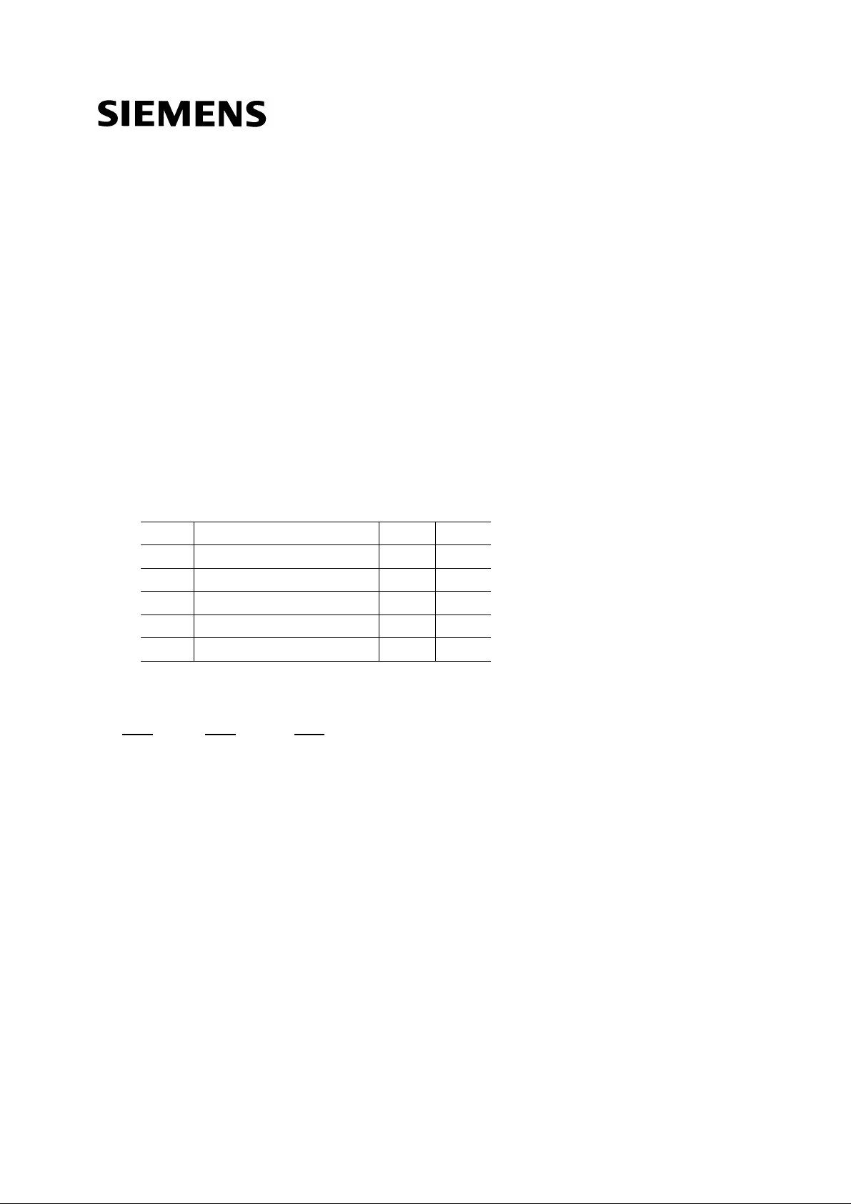
• Performance:
-50 -60
tRAC RAS Access Time 50 ns 60 ns
tCAC CAS Access Time 13 ns 15 ns
tAA Access Time from Address 25 ns 30 ns
tRC Cycle Time 84 ns 104 ns
tHPC EDO Mode Cycle Time 20 ns 2 5 ns
• Single +3.3 V ± 0.3 V Power Supply
• CAS-before-RAS refresh, RAS-only-refresh
• Decoupling capacitors mounted on substrate
• All inputs, outputs and clocks are fully LV-TTL compatible
• Serial presence detects (optional)
• Utilizes 4M x 4 -DRAMs in TSOPII packages
• 2048 refresh cycles / 32 ms with 11 / 11 addressing ( Row / Column) for HYM64/72V4005GU
• 4096 refresh cycles / 64 ms with 12 / 10 addressing ( Row / Column) for HYM64/72V4045GU
• Gold contact pads
• Card Size: 133,35mm x 25,40 mm x 4,00 mm
• This DRAM product module family is intended to be fully pin and architecture compatible
with the 168pin unbuffered SDRAM DIMM module family
Semiconductor Group 1
1 2.97
HYM64(72)V4005/45GU-50/-60
4M x 64/72 DRAM Module
The HYM64(72)V4005/45GU-50/-60 are industry standard 168-pin 8-byte Dual In-Line Memory
Modules (DIMMs) which are organized as 4M x 64 and 4M x 72 high speed memory arrays
designed with EDO DRAMs for non-parity and ECC applications. 2k refresh with 11 / 11 addressing
and 4k refresh modules with 12 / 10 addressing are available. The DIMMs use sixteen 4M x 4 EDO
DRAMs for the 4M x 64 organisation and eighteen 4M x 4 DRAMs for the 4M x 72 organisation, both
in TSOPII packages. Decoupling capacitors are mounted on the PC board.
The DIMMs use optional serial presence detects implemented via a serial E
2
C protocol. The first 128 bytes are utilized by the DIMM manufacturer and the second 128
pin I
bytes of serial PD data are available to the customer.
All 168-pin DIMMs provide a high performance, flexible 8-byte interface in a 133,35 mm long spacesaving footprint.
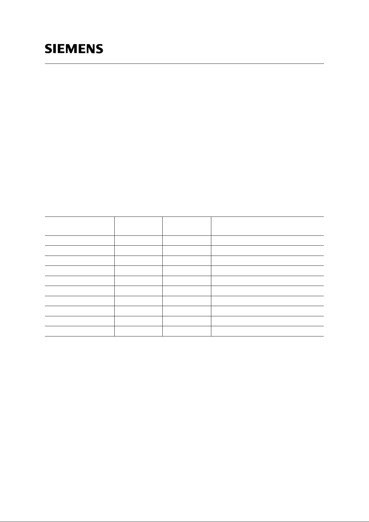
Ordering Information
2
PROM using the two
Type Ordering
Package Descriptions
Code
2k-Refresh:
HYM 64V4005GU-50 Q67100-Q2184 L-DIM-168-12 4M x 64 DRAM module (access time 50 ns)
HYM 64V4005GU-60 Q67100-Q2185 L-DIM-168-12 4M x 64 DRAM module (access time 60 ns)
HYM 72V4005GU-50 Q67100-Q2186 L-DIM-168-12 4M x 72 DRAM module (access time 50 ns)
HYM 72V4005GU-60 Q67100-Q2187 L-DIM-168-12 4M x 72 DRAM module (access time 60 ns)
4k-Refresh:
HYM 64V4045GU-50 L-DIM-168-12 4M x 64 DRAM module (access time 50 ns)
HYM 64V4045GU-60 L-DIM-168-12 4M x 64 DRAM module (access time 60 ns)
HYM 72V4045GU-50 L-DIM-168-12 4M x 72 DRAM module (access time 50 ns)
HYM 72V4045GU-60 L-DIM-168-12 4M x 72 DRAM module (access time 60 ns)
Semiconductor Group 2
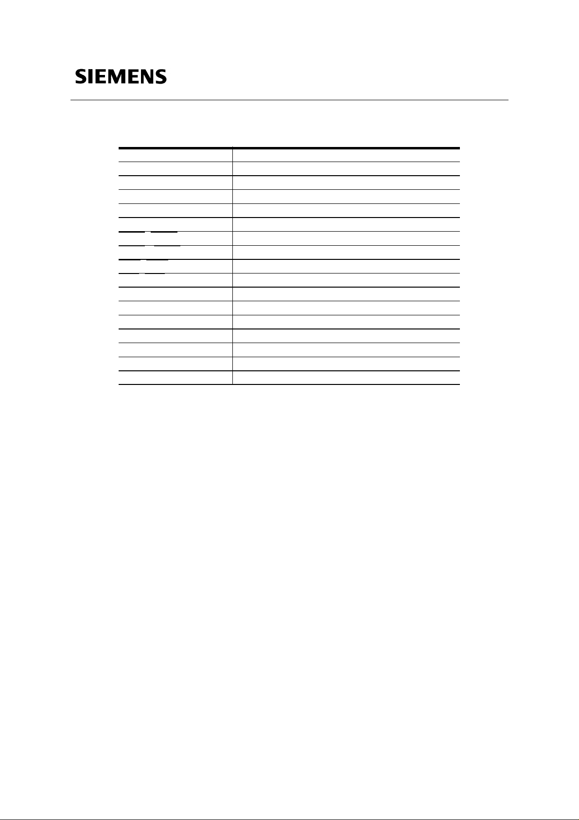
Pin Names
A0-A10 Row Address Input for HYB64/72V4005
A0-A10 Column Address Input for HYB64/72V4005
A0-A11 Row Address Input for HYB64/72V4045
A0-A9 Column Address Input for HYB64/72V4045
DQ0 - DQ63 Data Input/Output
CB0-CB7 Check Bit Data Input/Output ( x72 only)
RAS0
CAS0
WE0
OE0
Vcc Power (+3.3 Volt)
Vss Ground
SCL Clock for Presence Detect
SDA Serial Data Out for Presence Detect
SA0-SA2 Serial Presence Detect Addresses
N.C. No Connection
DU Don’t use
, RAS2 Row Address Strobe
- CAS7 Column Address Strobe
, WE2 Read / Write Input
, OE2 Output Enable
HYM64(72)V4005/45GU-50/-60
4M x 64/72 DRAM Module
Semiconductor Group 3
HYM64(72)V4005/45GU-50/-60
4M x 64/72 DRAM Module
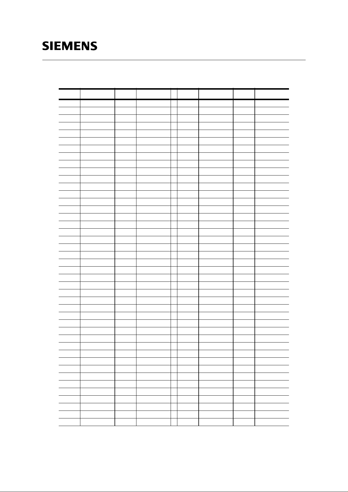
Pin Configuration
PIN # Symbol PIN # Symbol PIN # Symbol PIN # Symbol
1 VSS 43 VSS 85 VSS 127 VSS
2 DQ0 44 OE2 86 DQ32 128 DU
3 DQ1 45 RAS2 87 DQ33 129 NC
4 DQ2 46 CAS2 88 DQ34 130 CAS6
5 DQ3 47 CAS3 89 DQ35 131 CAS7
6 VCC 48 WE2 90 VCC 132 DU
7 DQ4 49 VCC 91 DQ36 133 VCC
8 DQ5 50 NC 92 DQ37 134 NC
9 DQ6 51 NC 93 DQ38 135 NC
10 DQ7 52 CB3 94 DQ39 136 CB6
11 DQ8 53 CB3 95 DQ40 137 CB7
12 VSS 54 VSS 96 VSS 138 VSS
13 DQ9 55 DQ16 97 DQ41 139 DQ48
14 DQ10 56 DQ17 98 DQ42 140 DQ49
15 DQ11 57 DQ18 99 DQ43 141 DQ50
16 DQ12 58 DQ19 100 DQ44 142 DQ51
17 DQ13 59 VCC 101 DQ45 143 VCC
18 VCC 60 DQ20 102 VCC 144 DQ52
19 DQ14 61 NC 103 DQ46 145 NC
20 DQ15 62 DU 104 DQ47 146 DU
21 CB0 63 NC 105 CB4 147 NC
22 CB1 64 VSS 106 CB5 148 VSS
23 VSS 65 DQ21 107 VSS 149 DQ53
24 NC 66 DQ22 108 NC 150 DQ54
25 NC 67 DQ23 109 NC 151 DQ55
26 VCC 68 VSS 110 VCC 152 VSS
27 WE0 69 DQ24 111 DU 153 DQ56
28 CAS0 70 DQ25 112 CAS4 154 DQ57
29 CAS1 71 DQ26 113 CAS5 155 DQ58
30 RAS0 72 DQ27 114 NC 15 6 DQ59
31 OE0 73 VCC 115 DU 157 VCC
32 VSS 74 DQ28 116 VSS 158 DQ60
33 A0 75 DQ29 117 A1 159 DQ61
34 A2 76 DQ30 118 A3 160 DQ62
35 A4 77 DQ31 119 A5 161 DQ63
36 A6 78 VSS 120 A7 162 VSS
37 A8 79 NC 121 A9 163 NC
38 A10 80 NC 122 A11 164 NC
39 NC 81 NC 123 NC 165 SA0
40 VCC 82 SDA 124 VCC 166 SA1
41 VCC 83 SCL 125 DU 167 SA2
42 DU 84 VCC 126 DU 168 VCC
Semiconductor Group 4
HYM64(72)V4005/45GU-50/-60
4M x 64/72 DRAM Module
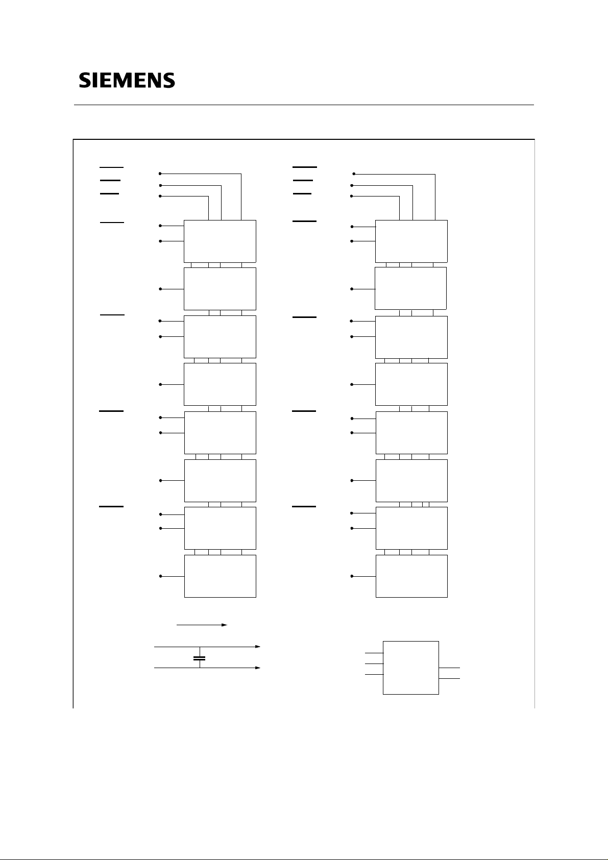
RAS0
WE0
OE0
CAS0
DQ0-DQ3
DQ4-DQ7
CAS1
DQ8-DQ11
DQ12-DQ15
CAS2
DQ16-DQ19
I/O1-I/O4
I/O1-I/O4
I/O1-I/O4
I/O1-I/O4
I/O1-I/O4
D0
D1
D2
D3
D4
RAS2
WE2
OE2
CAS4
DQ32-DQ35
D36-DQ39
CAS5
DQ40-DQ43
DQ44-DQ47
CAS6
DQ48-DQ51
I/O1-I/O4
D8
I/O1-I/O4
D9
I/O1-I/O4
D10
I/O1-I/O4
D11
I/O1-I/O4
D12
D20-DQ23
CAS3
DQ24-DQ27
DQ28-DQ31
A0-A10,(A11)
VCC
VSS
I/O1-I/O4
D5
I/O1-I/O4
D6
I/O1-I/O4
D7
D0-D15
C0-C15
4M x 64 DIMM Module Block Diagram
DQ52-DQ55
CAS7
DQ56-DQ59
DQ60-DQ63
I/O1-I/O4
D13
I/O1-I/O4
D14
I/O1-I/O4
D15
E2PROM (256wordx8bit)
SA0
SA1
SCL
SA2
SDA
Semiconductor Group 5
HYM64(72)V4005/45GU-50/-60
4M x 64/72 DRAM Module
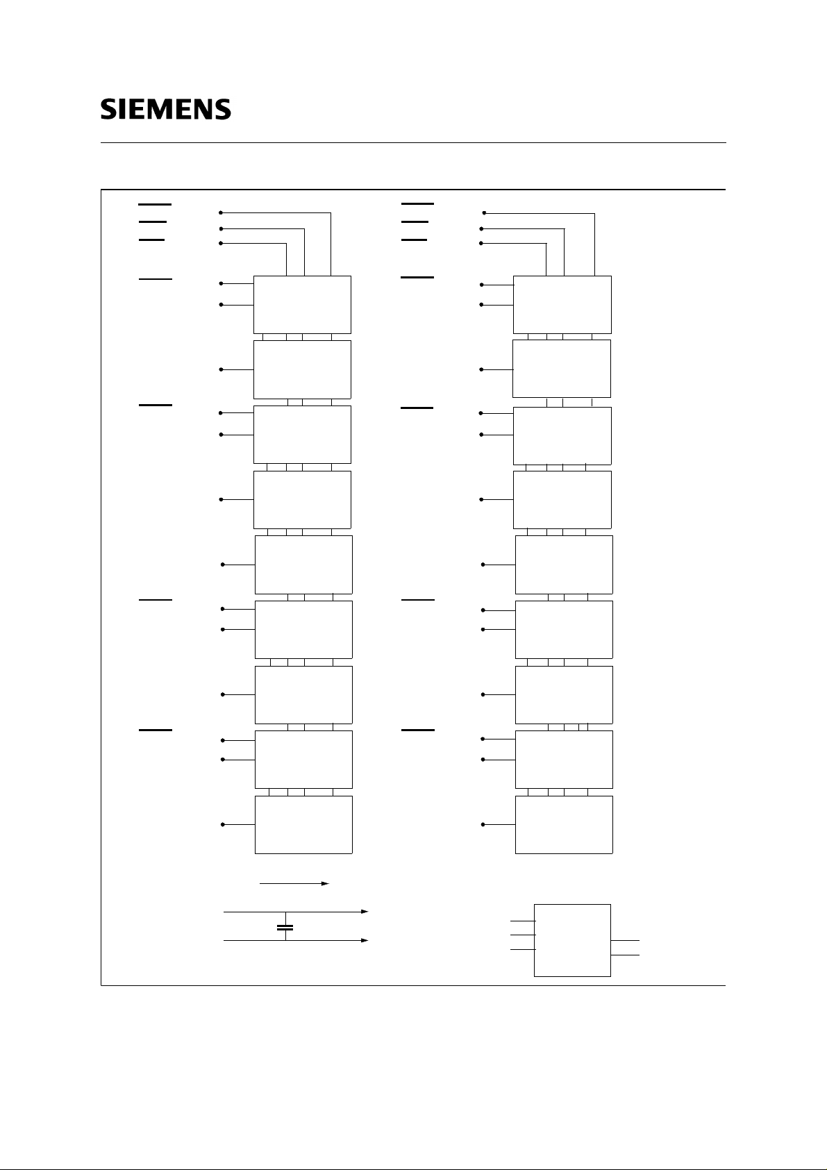
RAS0
WE0
OE0
CAS0
DQ0-DQ3
DQ4-DQ7
CAS1
DQ8-DQ11
DQ12-DQ15
CB0-CB3
CAS2
DQ16-DQ19
I/O1-I/O4
I/O1-I/O4
I/O1-I/O4
I/O1-I/O4
I/O1-I/O4
I/O1-I/O4
D0
D1
D2
D3
D16
D4
RAS2
WE2
OE2
CAS4
DQ32-DQ35
D36-DQ39
CAS5
DQ40-DQ43
DQ44-DQ47
CB4-CB7
CAS6
DQ48-DQ51
I/O1-I/O4
D8
I/O1-I/O4
D9
I/O1-I/O4
D10
I/O1-I/O4
D11
I/O1-I/O4
D17
I/O1-I/O4
D12
D20-DQ23
CAS3
DQ24-DQ27
DQ28-DQ31
A0-A10,(A11)
VCC
VSS
I/O1-I/O4
I/O1-I/O4
I/O1-I/O4
C0-C17
DQ52-DQ55
D5
CAS7
DQ56-DQ59
D6
DQ60-DQ63
D7
D0-D17
4M x 72 DIMM Module Block Diagram
Semiconductor Group 6
I/O1-I/O4
D13
I/O1-I/O4
D14
I/O1-I/O4
D15
E2PROM (256wordx8bit)
SA0
SA1
SCL
SA2
SDA
 Loading...