

Siemens HYM364020GS-60, HYM364020S-60 Datasheet

4M x 36-Bit Dynamic RAM Module HYM 364020S/GS-60
• SIMM modules with 4 194 304 words by 36-Bit organization
for PC main memory applications
• Fast access and cycle time
60 ns access time
110 ns cycle time (-60 version)
• Fast page mode capability
40 ns cycle time (-60 version)
• Single + 5 V (± 10 %) supply
• Low power dissipation
max. 7260 mW active (-60 version)
CMOS – 66 mW standby
TTL –132 mW standby
• CAS-before-RAS refresh
RAS-only-refresh
Hidden-refresh
• 12 decoupling capacitors mounted on substrate
• All inputs, outputs and clocks fully TTL compatible
• 72 pin Single in-Line Memory Module (L-SIM-72-12) with 22.9 mm (900 mil) height
• Utilizes eight 4Mx4-DRAMs and four 4Mx1-DRAMs in SOJ packages
• 2048 refresh cycles / 32 ms
• Optimized for use in byte-write parity applications
• Tin-Lead contact pads (S-version)
• Gold contact pads (GS - version)
Semiconductor Group 1
6.95
HYM 364020S/GS-60
4M × 36-Bit
The HYM 364020S/GS-60 is a 16 MByte DRAM module organized as 4 194 304 words by 36Bit in a 72-pin single-in-line package comprising eight HYB 5117400BJ 4M × 4 DRAMs and four
HYB 514100BJ 4M x 1 DRAMS in 300 mil wide SOJ-packages mounted together with twelve 0.2 µF
ceramic decoupling capacitors on a PC board.
The HYM 364020S/GS-60 can also be used as a 8 388 608 words by 18-bits dynamic RAM module
by means of connecting DQ0 and DQ18, DQ1 and DQ19, DQ2 and DQ20, … , DQ17 and DQ35,
respectively.
Each HYB 5117400BJ and HYB 514100BJ is described in the data sheet and is fully electrical
tested and processed according to SIEMENS standard quality procedure prior to module assembly.
After assembly onto the board, a further set of electrical tests is performed.
The speed of the module can be detected by the use of four presence detect pins.
The common I/O feature on the HYM 364020S/GS-60 dictates the use of early write cycles.
Ordering Information
Type Ordering Code Package Description
HYM 364020S-60 Q67100-Q2006 L-SIM-72-12 DRAM Module
(access time 60 ns)
HYM 364020GS-60 Q67100-Q982 L-SIM-72-12 DRAM Module
(access time 60 ns)
Semiconductor Group 2
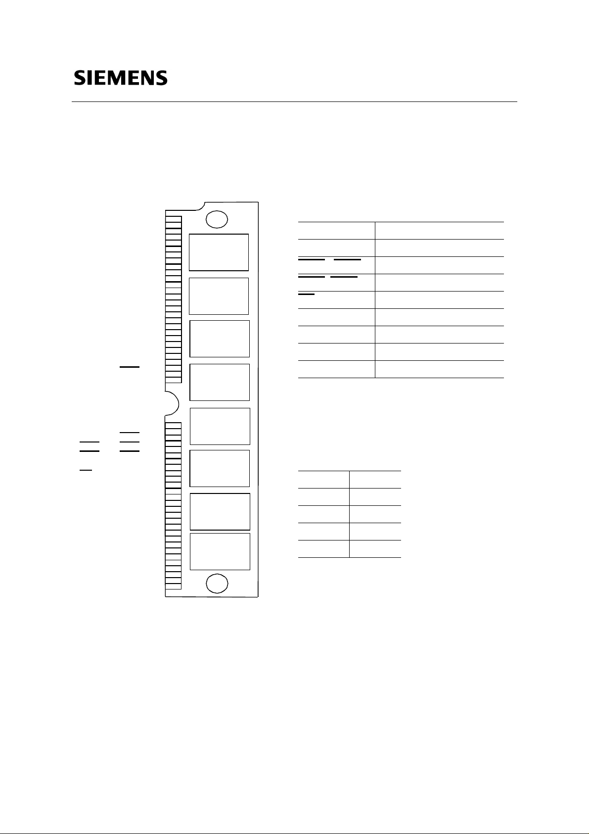
Pin Configuration
VSS 1 DQ0 2
DQ18 3 DQ1 4
DQ19 5 DQ2 6
DQ20 7 DQ3 8
DQ21 9 VCC 10
N.C. 11 A0 12
A1 13 A2 14
A3 15 A4 16
A5 17 A6 18
A10 19 DQ4 20
DQ22 21 DQ5 22
DQ23 23 DQ6 24
DQ24 25 DQ7 26
DQ25 27 A7 28
N.C. 29 VCC 30
A8 31 A9 32
N.C. 33 RAS2
DQ26 35 DQ8 36
34
HYM 364020S/GS-60
4M × 36-Bit
Pin Names
A0-A10 Address Inputs
DQ0-DQ35 Data Input/Output
- CAS3 Column Address Strobe
CAS0
, RAS2 Row Address Strobe
RAS0
WE
V
CC
V
SS
PD Presence Detect Pin
N.C. No Connection
Read/Write Input
Power (+ 5 V)
Ground
DQ17 37 DQ35 38
VSS 39 CAS0
CAS2
41 CAS3 42
CAS1
43 RAS0 44
N.C. 45 N.C. 46
WE
47 N.C. 48
DQ9 49 DQ2750
DQ10 51 DQ28 52
DQ11 53 DQ29 54
DQ12 55 DQ30 56
DQ13 57 DQ31 58
VCC 59 DQ32 60
DQ14 61 DQ33 62
DQ15 63 DQ34 64
DQ16 65 N.C. 66
PD0 67 PD1 68
PD2 69 PD3 70
N.C. 71 VSS 72
40
Presence Detect Pins
-60
PD0
V
SS
PD1 N.C.
PD2 N.C.
PD3 N.C.
Semiconductor Group 3
 Loading...