

Siemens HYM322030GS-70, HYM322030S-60, HYM322030S-70 Datasheet
Semiconductor Group 561 09.94
2M x 32-Bit Dynamic RAM Module
Advanced Information
HYM 322030S/GS-60/-70
• 2 097 152 words by 32-bit organization
• Fast access and cycle time
60 ns access time
110 ns cycle time (-60 version)
70 ns access time
130 ns cycle time (-70 version)
• Fast page mode capability
40 ns cycle time (-60 version)
45 ns cycle time (-70 version)
• Single + 5 V (± 10 %) supply
• Low power dissipation
max. 3300 mW active (-60 version)
max. 3025 mW active (-70 version)
CMOS – 22 mW standby
TTL – 44 mW standby
Ordering Information
Type Ordering Code Package Description
HYM 322030S-60 Q67100-Q976 L-SIM-72-9 DRAM Module
(access time 60 ns)
HYM 322030S-70 Q67100-Q977 L-SIM-72-9 DRAM Module
(access time 70 ns)
HYM 322030GS-60 Q67100-Q2018 L-SIM-72-9 DRAM Module
(access time 60 ns)
HYM 322030GS-70 Q67100-Q2019 L-SIM-72-9 DRAM Module
(access time 70 ns)
• CAS-before-RAS refresh
RAS-only-refresh
Hidden-refresh
• 4 decoupling capacitors mounted on
substrate
• All inputs, outputs and clocks fully TTL
compatible
• 72 pin Single in-Line Memory Module
(L-SIM-72-9 ) with 20.32 mm (800 mil) height
• Utilizes four 2M × 8 - DRAMs in 400 mil
SOJ-packages
• 2048 refresh cycles / 32 ms
• Tin-Lead contact pads (S - version)
• Gold contact pads (GS - version)
Semiconductor Group 562
HYM 322030S/GS-60/-70
2M × 32-Bit
The HYM 322030S/GS-60/-70 is a 8 M Byte DRAM module organized as 2 097 152 words by
32-bit in a 72-pin single-in-line package comprising four HYB 5117800BSJ 2M × 8 DRAMs in 400
mil wide SOJ-packages mounted together with four 0.2 µF ceramic decoupling capacitors on a PC
board.
Each HYB 5117800BSJ is described in the data sheet and is fully electrical tested and processed
according to SIEMENS standard quality procedure prior to module assembly. After assembly onto
the board, a further set of electrical tests is performed.
The speed of the module can be detected by the use of four presence detect pins.
The common I/O feature on the HYM 322030S/GS-60/-70 dictates the use of early write cycles.
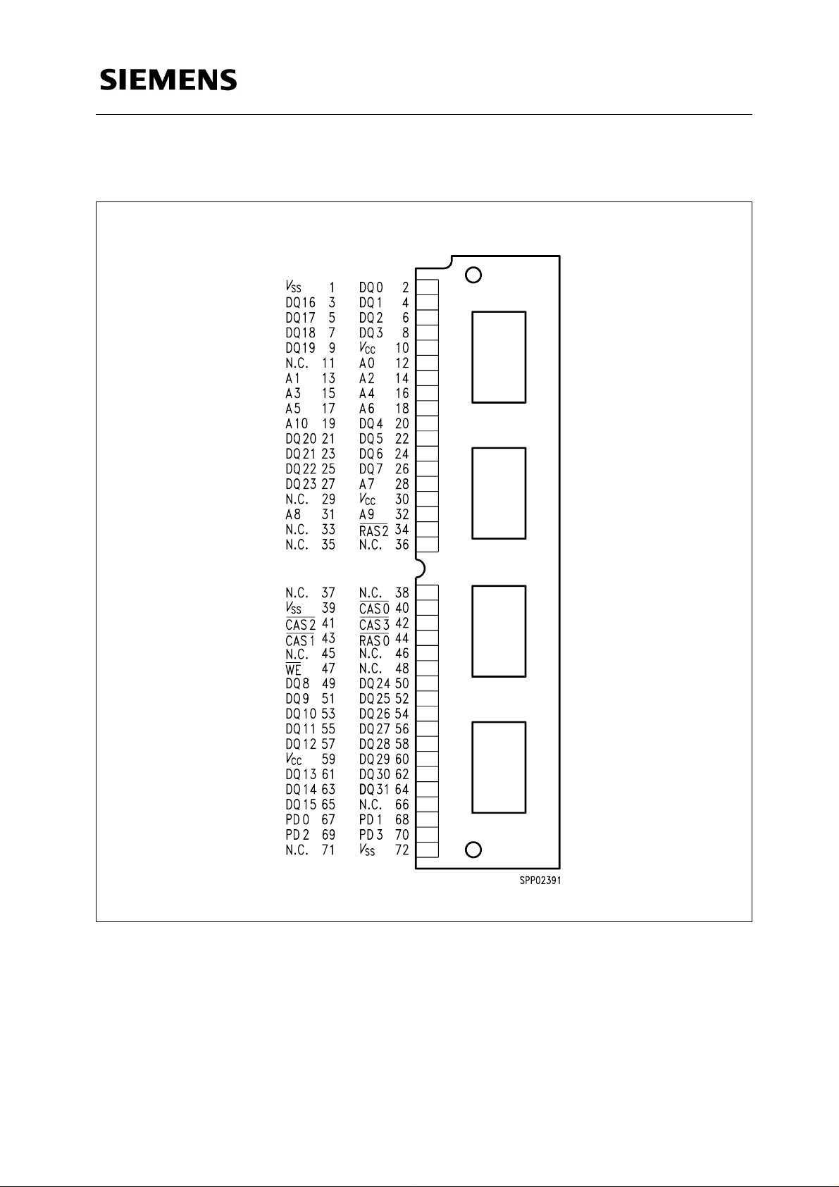
Pin Definitions and Functions
Presence Detect Pins
Pin No. Function
A0R-A10R Row Address Inputs
A0C-A9C Column Address Inputs
DQ0-DQ31 Data Input/Output
CAS0 - CAS3 Column Address Strobe
RAS0, RAS2 Row Address Strobe
WE Read/Write Input
V
CC
Power (+ 5 V)
V
SS
Ground
PD Presence Detect Pin
N.C. No Connection
-60 -70
PD0 N.C. N.C.
PD1 N.C. N.C.
PD2 N.C.
V
SS
PD3 N.C. N.C.
Semiconductor Group 563
HYM 322030S/GS-60/-70
2M × 32-Bit
Pin Configuration
(top view)
 Loading...