

Siemens HYB514405BJ-50, HYB514405BJ-60, HYB514405BJ-70, HYB514405BJL-50, HYB514405BJL-60 Datasheet
...
1M x 4-Bit Dynamic RAM
(Hyper Page Mode (EDO) version)
Preliminary Information
• 1 048 576 words by 4-bit organization
• 0 to 70 ˚C operating temperature
• Hyper Page Mode - EDO
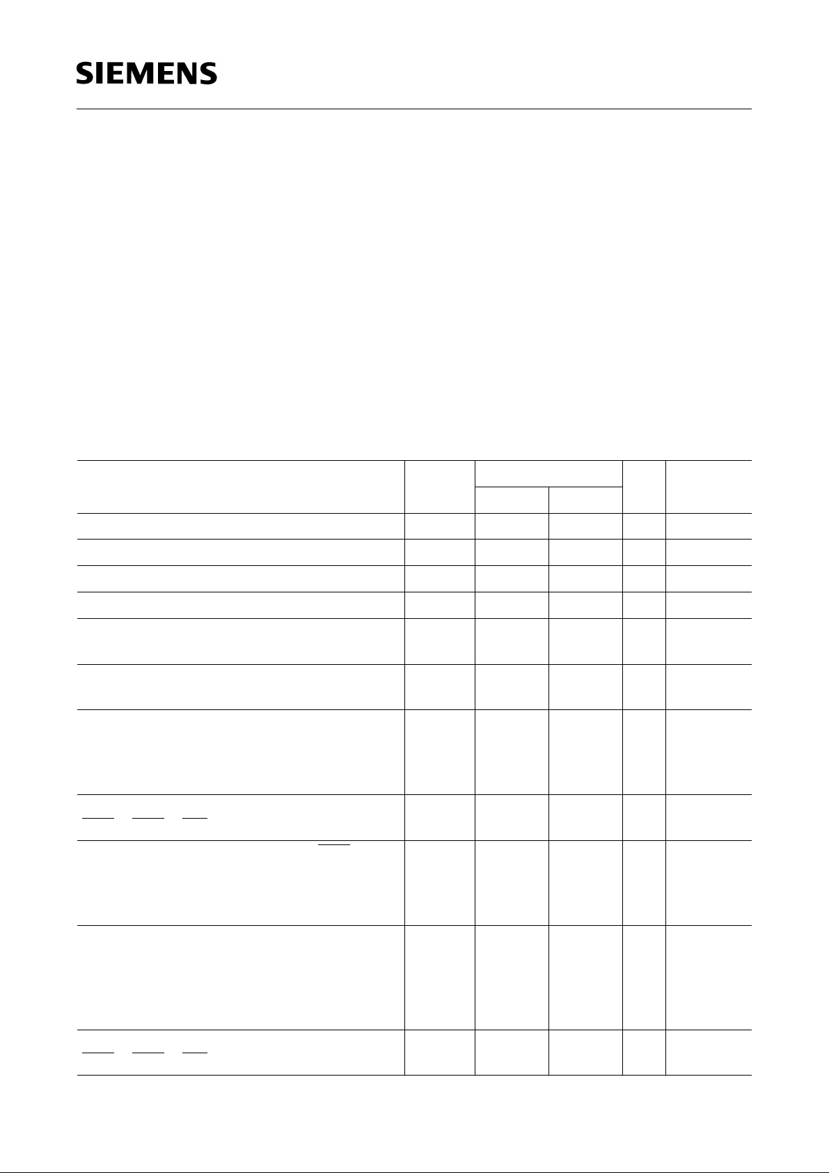
• Performance:
HYB 514405BJ/BJL-50/-60/-70
-50 -60 -70
t
t
t
t
t
RAC
CAC
AA
RC
HPC
RAS access time 50 60 70 ns
CAS access time 13 15 20 ns
Access time from address 25 30 35 ns
Read/Write cycle time 89 104 124 ns
Hyper page mode (EDO)
20 25 30 ns
cycle time
• Single + 5 V (± 10 %) supply
• Low power dissipation
max. 660 mW active (-50 version)
max. 605 mW active (-60 version)
max. 550 mW active (-70 version)
• Standby power dissipation:
11 mW max.standby (TTL)
5.5 mW max.standby (CMOS)
1.1 mW max.standby (CMOS) for Low Power Version
• Read, write, read-modify write, CAS-before-RAS refresh, RAS-only refresh,
hidden refresh and test mode capability
• All inputs and outputs TTL-compatible
• 1024 refresh cycles / 16 ms
• 1024 refresh cycles / 128 ms for Low Power Version
• Plastic Packages: P-SOJ-26/20-5 with 300 mil width
Semiconductor Group 1 5.96
HYB 514405BJ/BLJ-50/-60/-70
1M x 4 EDO - DRAM
The HYB 514405BJ is the new generation dynamic RAM organized as 1 048 576 words by 4-bit.
The HYB 514405BJ utilizes CMOS silicon gate process as well as advances circuit techniques to
provide wide operation margins, both internally and for the system user. Multiplexed address inputs
permit the HYB 514405BJ to be packed in a standard plastic P-SOJ-26/20 package. This package
size provides high system bit densities and is compatible with commonly used automatic testing and
insertion equipment. System oriented feature include single + 5 V (± 10 %) power supply, direct
interfacing with high performance logic device families.
Ordering Information
Type Ordering Code Package Descriptions
HYB 514405BJ-50 Q67100-Q2116 P-SOJ-26/20-5 EDO-DRAM
(access time 50 ns)
HYB 514405BJ-60 Q67100-Q2118 P-SOJ-26/20-5 EDO-DRAM
(access time 60 ns)
HYB 514405BJ-70 Q67100-Q2120 P-SOJ-26/20-5 EDO-DRAM
(access time 70 ns)
HYB 514405BJL-50 on request P-SOJ-26/20-5 Low Power EDO-DRAM
(access time 50 ns)
HYB 514405BJL-60 on request P-SOJ-26/20-5 Low Power EDO-DRAM
(access time 60 ns)
HYB 514405BJL-70 on request P-SOJ-26/20-5 Low Power EDO-DRAM
(access time 70 ns)
Semiconductor Group 2
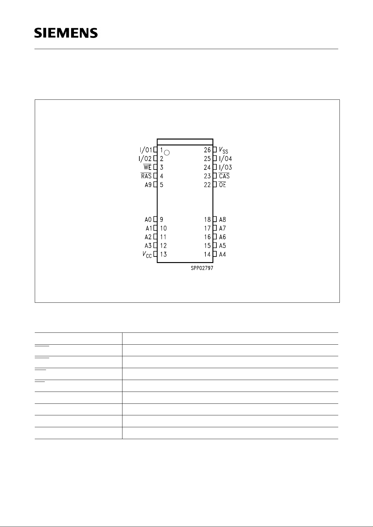
Pin Configuration
(top view)
HYB 514405BJ/BJL-50/-60/-70
1M x 4 EDO - DRAM
P-SOJ-26/20-5
Pin Names
A0-A9 Address Input
RAS Row Address Strobe
CAS Column Address Strobe
WE Read/Write Input
OE Output Enable
I/O1 - I/O4 Data Input/Output
V
CC
V
SS
Power Supply (+ 5 V)
Ground (0 V)
N.C. No Connection
Semiconductor Group 3
HYB 514405BJ/BLJ-50/-60/-70
1M x 4 EDO - DRAM
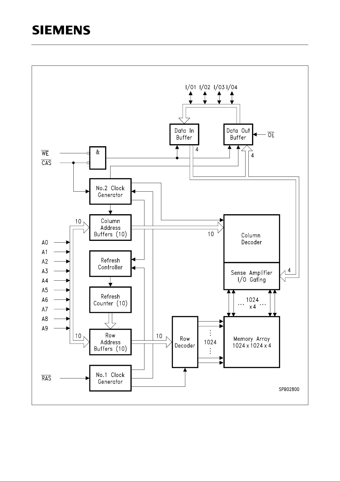
Block Diagram
Semiconductor Group 4
HYB 514405BJ/BJL-50/-60/-70
1M x 4 EDO - DRAM
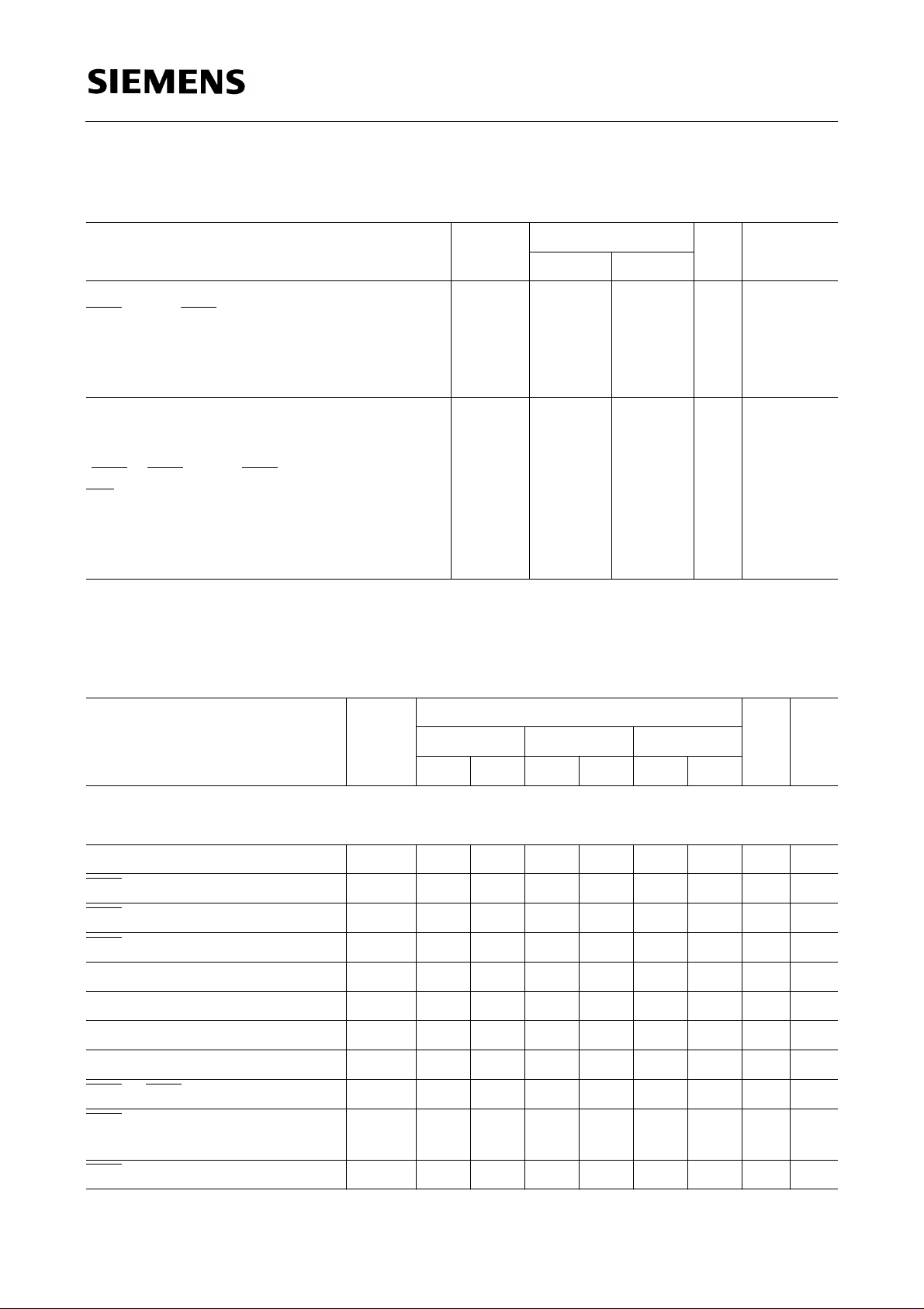
Absolute Maximum Ratings
Operating temperature range ............................................................................................0 to 70 ˚C
Storage temperature range......................................................................................– 55 to + 150 ˚C
Input/output voltage ........................................................................................................– 1 to + 7 V
Power Supply voltage.....................................................................................................– 1 to + 7 V
Data out current (short circuit) ................................................................................................50 mA
Note:
Stresses above those listed under "Absolute Maximum Ratings" may cause permanent
damage of the device. Exposure to absolute maximum rating conditions for extended periods
may affect device reliability.
DC Characteristics
T
= 0 to 70 ˚C, VSS = 0 V, VCC = 5 V ± 10 %, tT = 2 ns
A
Parameter Symbol Limit Values Unit Test
Condition
1)
1)
1)
1)
1)
Input high voltage
Input low voltage V
Output high voltage (I
Output low voltage (I
= – 5 mA) V
OUT
= 4.2 mA) V
OUT
Input leakage current, any input
min. max.
V
ih
il
oh
ol
I
I(L)
2.4 VCC + 0.5 V
– 1.0 0.8 V
2.4 – V
– 0.4 V
– 10 10 µA
(0 V < Vin < 7, all other input = 0 V)
Output leakage current
(DO is disabled, 0 < V
OUT
< VCC)
Average VCC supply current
-50 version
-60 version
-70 version
I
I
o(L)
CC1
– 10 10 µA
mA
–
–
–
120
110
100
1)
2) 3)4)
Standby VCC supply current
(RAS = CAS = WE = Vih)
V
Average
supply current during RAS-only
CC
refresh cycles -50 version
-60 version
-70 version
Average VCC supply current during hyper page
mode(EDO) operation
-50 version
-60 version
-70 version
Standby VCC supply current
(RAS = CAS = WE = VCC – 0.2 V)
Semiconductor Group 5
I
I
I
I
CC2
CC3
CC4
CC5
–2mA–
2)4)
2) 3)4)
–
–
–
–
–
–
120
110
100
100
90
80
–1
200
mA
mA
mA
µA1) L-version
HYB 514405BJ/BLJ-50/-60/-70
1M x 4 EDO - DRAM
DC Characteristics (cont’d)
T
= 0 to 70 ˚C, VSS = 0 V, VCC = 5 V ± 10 %, tT = 2 ns
A
Parameter Symbol Limit Values Unit Test
Condition
2)4)
Average VCC supply current during
CAS before RAS refresh mode
-50 version
-60 version
-70 version
I
CC6
min. max.
–
–
–
120
110
100
mA
For Low Power Version only:
Battery backup current (average power supply
current in battery backup mode):
(CAS = CAS before RAS cycling or 0.2 V,
WE = VCC – 0.2 V or 0.2 V,
A0 to A10 = VCC – 0.2 V or 0.2 V;
DI = VCC – 0.2 V or 0.2 V or open,
t
= 125 µs, t
RC
AC Characteristics
T
= 0 to 70 ˚C, VCC = 5 V ± 10 %, tT = 2 ns
A
Parameter
RAS
= t
min = 1 µs)
RAS
5)6)
Symbol
min. max. min. max. min. max.
Common Parameters
Random read or write cycle time t
RAS precharge time t
RAS pulse width t
CAS pulse width t
Row address setup time
Row address hold time
Column address setup time
Column address hold time
RAS to CAS delay time t
RAS to column address delay
RC
RP
RAS
CAS
t
ASR
t
RAH
t
ASC
t
CAH
RCD
t
RAD
89 – 104 – 124 – ns
35 – 40 – 50 – ns
50 10k 60 10k 70 10k ns
8 10k 10 10k 12 10k ns
0–0–0–ns
8–10–10–ns
0–0–0–ns
8–10–12–ns
12 37 14 45 14 53 ns
10 25 12 30 12 35 ns
time
I
CC7
– 250 µA–
Limit Values
-50 -60 -70
Unit Note
RAS hold time t
RSH
13 15 – 17 – ns
Semiconductor Group 6
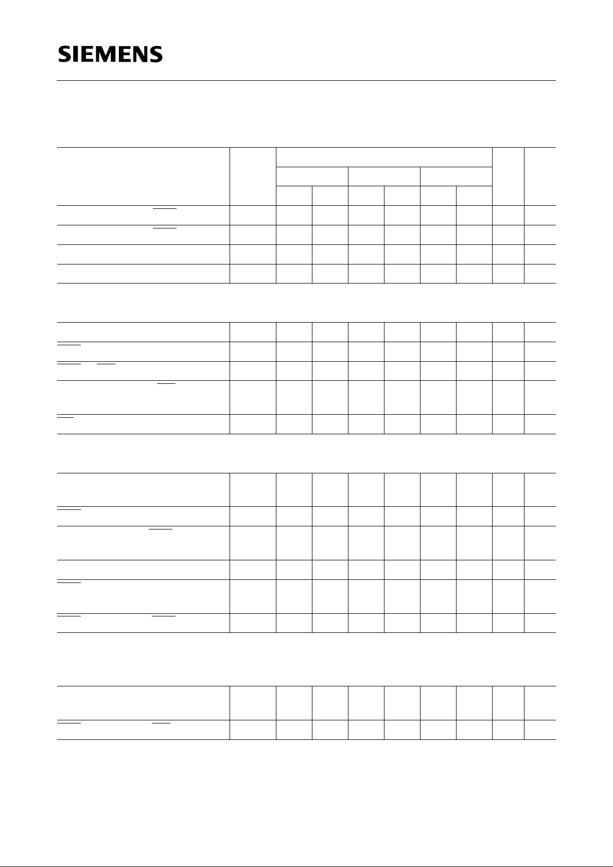
HYB 514405BJ/BJL-50/-60/-70
1M x 4 EDO - DRAM
AC Characteristics (cont’d)
T
= 0 to 70 ˚C, VCC = 5 V ± 10 %, tT = 2 ns
A
Parameter
CAS hold time t
CAS to RAS precharge time t
Transition time (rise and fall)
Refresh period
Refresh period for L-version
5)6)
Symbol
CSH
CRP
t
T
t
REF
t
REF
Read Cycle
Access time from RAS t
Access time from
CAS t
Access time from column
RAC
CAC
t
AA
address
Limit Values
Unit Note
-50 -60 -70
min. max. min. max. min. max.
50 60 – 70 – ns
5–5–5–ns
150150150ns7
–16–16–16ms
– 128 – 128 – 128 ms
– 50 – 60 – 70 ns 8, 9
– 13 – 15 – 17 ns 8, 9
– 25 – 30 – 35 ns 8,10
OE access time t
Column address to
RAS lead
time
Read command setup time
Read command hold time
Read command hold time
referenced to
RAS
CAS to output in low-Z t
Output buffer turn-off delay
Output buffer turn-off delay from
OE
Data to
Data to
CAS low delay t
OE low delay t
CAS high to data delay t
OE high to data delay t
Write Cycle
OEA
t
RAL
t
RCS
t
RCH
t
RRH
CLZ
t
OFF
t
OEZ
DZC
DZO
CDD
ODD
–13–15–17ns
25 – 30 – 35 – ns
0–0–0–ns
0–0–0–ns11
0–0–0–ns11
0–0–0–ns8
013015017ns12
013015017ns12
0–0–0–ns13
0–0–0–ns13
10 – 13 – 15 – ns 14
10 – 13 – 15 – ns 14
Write command hold time t
Write command pulse width
Write command setup time
WCH
t
WP
t
WCS
8–10–10–ns
8–10–10–ns
0–0–0–ns15
Semiconductor Group 7
HYB 514405BJ/BLJ-50/-60/-70
1M x 4 EDO - DRAM
AC Characteristics (cont’d)
T
= 0 to 70 ˚C, VCC = 5 V ± 10 %, tT = 2 ns
A
Parameter
Write command to RAS lead time t
Write command to
CAS lead time t
Data setup time
Data hold time
5)6)
Symbol
RWL
CWL
t
DS
t
DH
Read-modify-Write Cycle
Read-write cycle time t
RAS to WE delay time t
CAS to WE delay time t
Column address to
WE delay
RWC
RWD
CWD
t
AWD
time
Limit Values
Unit Note
-50 -60 -70
min. max. min. max. min. max.
13 – 15 – 17 – ns
13 – 15 – 17 – ns
0–0–0–ns16
8–10–12–ns16
118 – 138 – 162 – ns
64 – 77 – 89 – ns 15
27 – 32 – 36 – ns 15
39 – 47 – 54 – ns 15
OE command hold time t
Hyper Page Mode (EDO) Cycle
Hyper page mode (EDO) cycle
time
CAS precharge time t
Access time from
CAS
precharge
Output data hold time
RAS pulse width in hyper page
mode
CAS precharge to RAS Delay t
Hyper Page Mode (EDO) Readmodify-Write Cycle
Hyper page mode (EDO) readwrite cycle time
OEH
t
HPC
CP
t
CPA
t
COH
t
RAS
RHCP
t
PRWC
10 – 13 – 15 – ns
20 – 25 – 30 – ns
8–10–10–ns
–27–32–37ns7
5–5–5–ns
50 200k 60 200k 70 200k ns
27 – 32 – 37 – ns
58 – 68 – 77 – ns
CAS precharge to WE t
CPWD
41 – 49 – 56 – ns
Semiconductor Group 8
 Loading...