

Siemens HYB5116165BJ-70, HYB5116165BJ-50, HYB5116165BJ-60, HYB5118165BJ-50, HYB5118165BJ-60 Datasheet
...
1M x 16-Bit Dynamic RAM
1k & 4k Refresh
(Hyper Page Mode- EDO)
Advanced Information
1 048 576 words by 16-bit organization
•
0 to 70 °C operating temperature
•
Performance:
•
HYB5116165BSJ -50/-60/-70
HYB5118165BSJ -50/-60/-70
-50 -60 -70
t
RAC
t
CAC
t
AA
t
RC
t
HPC
RAS
access time 50 60 70 ns
access time 13 15 20 ns
CAS
Access time from address 25 30 35 ns
Read/Write cycle time 84 104 124 ns
Hyper page mode (EDO)
20 25 30 ns
cycle time
Single + 5 V (± 10 %) supply
•
Low power dissipation
•
max. 1100 active mW ( HYB5118165BSJ-50)
max. 990 active mW ( HYB5118165BSJ-60)
max. 880 active mW ( HYB5118165BSJ-70)
max. 550 active mW ( HYB5116165BSJ-50)
max. 495 active mW ( HYB5116165BSJ-60)
max. 440 active mW ( HYB5116165BSJ-70)
11 mW standby (TTL)
5.5. mW standby (MOS)
Output unlatched at cycle end allows two-dimensional chip selection
•
Read, write, read-modify-write, CAS-before-RAS refresh, RAS-only refresh, hidden refresh
•
and Self Refresh
Hyper page mode (EDO) capability
•
All inputs, outputs and clocks fully TTL-compatible
•
1024 refresh cycles / 16 ms for HYB5118165BSJ (1k-Refresh)
•
4096 refresh cycles / 64 ms for HYB5116165BSJ (4k-Refresh)
•
Plastic Package: P-SOJ-42-1 400 mil
•
Semiconductor Group 1 1.96
HYB 5116(8)165BSJ-50/-60/-70
1M x 16-EDO DRAM
The HYB 5116(8)165BSJ is a 16 MBit dyn amic RAM organized as 1 048 576 words by 16 -bits. The
HYB 5116(8)165BSJ utilizes a submicron CMOS silicon gate process technology, as well as
advanced circuit techniques to provide wide operating margins, both internally and for the system
user. Multiplexed address inputs permit the HYB 5116(8)165BSJ to be packaged in a standard
SOJ 42 plastic package with 400 mil width. These packag es provide high sys tem bit densities and
are compatible with commonly used automatic testing and insertion equipment. System-oriented
features include single + 5 V (± 10 %) power supply, direct interfacing wit h hig h-performanc e l ogic
device families such as Schottky TTL.
Ordering Information
Type Ordering Code Package Descriptions
HYB 5116165BJ-50 on request P-SOJ-42-1 400 mil DRAM (access time 50 ns)
HYB 5116165BJ-60 on request P-SOJ-42-1 400 mil DRAM (access time 60 ns)
HYB 5116165BJ-70 on request P-SOJ-42-1 400 mill DRAM (access time 70 ns)
HYB 5118165BJ-50 Q67100-Q1107 P-SOJ-42-1 400 mil DRAM (access time 50 ns)
HYB 5118165BJ-60 Q67100-Q1108 P-SOJ-42-1 400 mil DRAM (access time 60 ns)
HYB 5118165BJ-70 Q67100-Q1109 P-SOJ-42-1 400 mil DRAM (access time 70 ns)
Pin Names
A0-A9 Row Address Inputs for HYB5118165BSJ
A0-A9 Column Address Inputs for HYB5118165BSJ
A0-A11 Row Address Inputs for HYB5116165BSJ
A0 to A7 Column Address Inputs for HYB5116165BSJ
RAS
OE
Row Address Strobe
Output Enable
I/O1-I/O16 Data Input/Output
UCAS
LCAS
WE
V
CC
V
SS
Upper Column Address Strobe
Lower Column Address Strobe
Read/Write Input
Power Supply (+ 5 V)
Ground (0 V)
N.C. not connected
Semiconductor Group 2
HYB 5116(8)165BSJ-50/-60/-70
P-SOJ-42-1 400 mil
1M x 16-EDO DRAM
Vcc
I/O1
I/O2
I/O3
I/O4
Vcc
I/O5
I/O6
I/O7
I/O8
N.C.
N.C.
WE
RAS
N.C.
N.C.
A0
A1
A2
A3
Vcc
1
2
3
4
5
6
7
8
9
10
11
12
13
14
15
16
17
18
19
20
21
HYB3118165BSJ
42
41
40
39
38
37
36
35
34
33
32
31
30
29
28
27
26
25
24
23
22
Vss
I/O16
I/O15
I/O14
I/O13
Vss
I/O12
I/O11
I/O10
I/O9
N.C.
LCAS
UCAS
OE
A9
A8
A7
A6
A5
A4
Vss
Vcc
I/O1
I/O2
I/O3
I/O4
Vcc
I/O5
I/O6
I/O7
I/O8
N.C.
N.C.
WE
RAS
A11
A10
A0
A1
A2
A3
Vcc
1
2
3
4
5
6
7
8
9
10
11
12
13
14
15
16
17
18
19
20
21
HYB3116165BSJ
42
41
40
39
38
37
36
35
34
33
32
31
30
29
28
27
26
25
24
23
22
Vss
I/O16
I/O15
I/O14
I/O13
Vss
I/O12
I/O11
I/O10
I/O9
N.C.
LCAS
UCAS
OE
A9
A8
A7
A6
A5
A4
Vss
Pin Configuration
Semiconductor Group 3
WE
HYB 5116(8)165BSJ-50/-60/-70
1M x 16-EDO DRAM
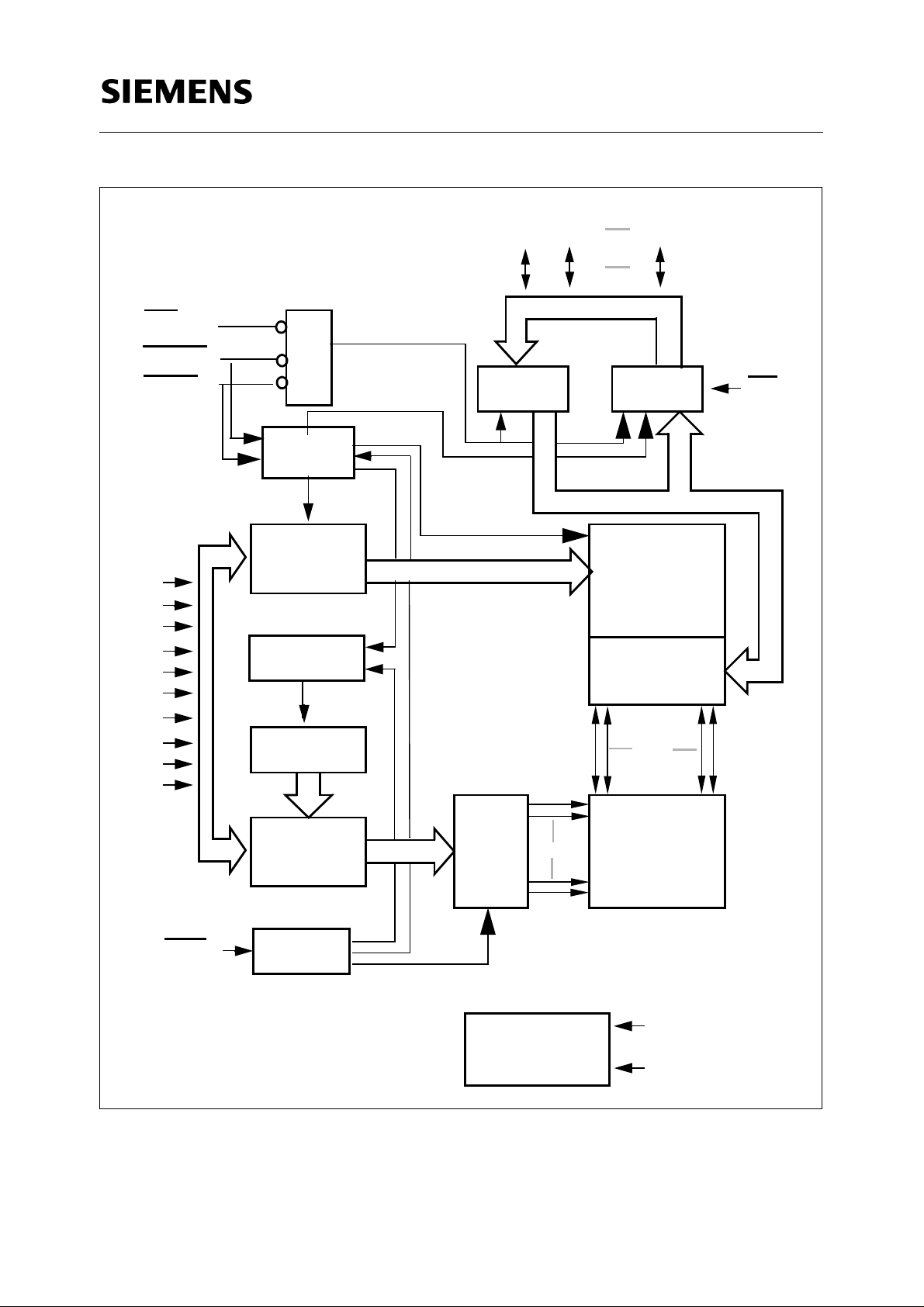
I
I/O1I/O2
/O16
UCAS
LCAS
A0
A1
A2
A3
A4
A5
A6
A7
A8
A9
A10
A11
.
&
.
No. 2 Clock
Generator
Column
8
12 12
Address
Buffer(8)
Refresh
Controller
Refresh
Counter (12)
Row
Address
Buffers(12)
12
Data in
Buffer
Row
Decoder
16
8
4096
Data out
Buffer
16
Column
Decoder
Sense Amplifier
I/O Gating
256
x16
Memory Array
4096x256x16
OE
16
No. 1 Clock
RAS
Block Diagram for HYB 5116165BSJ
Semiconductor Group 4
Generator
Voltage Down
Generator
VCC
VCC (internal)
WE
HYB 5116(8)165BSJ-50/-60/-70
1M x 16-EDO DRAM
I
I/O1I/O2
/O16
UCAS
LCAS
A0
A1
A2
A3
A4
A5
A6
A7
A8
A9
.
10
.
No. 2 Clock
Generator
Column
Buffer(10)
Refresh
Controller
Refresh
Counter (10)
&
Address
10
Data in
Buffer
16
10
Data out
Buffer
16
Column
Decoder
Sense Amplifier
I/O Gating
1024
x16
OE
16
Row
10 10
RAS
Block Diagram for HYB 5118165BSJ
Semiconductor Group 5
Address
Buffers(10)
No. 1 Clock
Generator
Row
Decoder
Voltage Down
1024
Generator
Memory Array
1024x1024x16
VCC
VCC (internal)
HYB 5116(8)165BSJ-50/-60/-70
1M x 16-EDO DRAM
Absolute Maximum Ratings
Operating temperature range ............................................................................................0 to 70 °C
Storage temperature range.........................................................................................– 55 to 150 °C
Input/output voltage................................................................................-0.5 to min (Vcc+0.5,7.0) V
Power supply voltage...................................................................................................-1.0V to 7.0 V
Power dissipation.....................................................................................................................1.0 W
Data out current (short circuit)................................................................................................50 mA
Note:
Stresses above those listed under “Absolute Maximum Ratings” may cause perm anent dama ge of
the device. Exposure to absolute maximu m rating conditions for extended perio ds may affect device
reliability.
DC Characteristics
= 0 to 70 °C,
T
A
( note : values in brackets for HYB5118165BSJ)
V
SS
= 0 V,
= 5 V ± 10 %; tT = 2 ns
V
CC
Parameter Symbol Limit Values Unit Test
mA
mA
mA
mA
mA
mA
Condition
1)
1)
1)
1)
1)
1)
2) 3) 4)
2) 4)
Input high voltage
Input low voltage
= – 5 mA)
Output high voltage (
Output low voltage (
I
OUT
= 4.2 mA)
I
OUT
Input leakage current
≤ Vcc + 0.3V, all other pins = 0 V)
(0 V ≤
V
IH
Output leakage current
(DO is disabled, 0 V ≤
Average
supply current:
V
CC
≤ Vcc + 0.3V)
V
OUT
-50 ns version
-60 ns version
-70 ns version
(RAS
, CAS, address cycling: tRC = tRC min.)
supply current (RAS =CAS=
Standby
Average
V
CC
supply current, during RAS-only
V
CC
refresh cycles: -50 ns version
-60 ns version
-70 ns version
(RAS
cycling, CAS =
, tRC = tRC min.)
V
IH
min. max.
V
IH
V
IL
V
OH
V
OL
I
I(L)
I
O(L)
I
CC1
)
V
I
IH
CC2
I
CC3
2.4 Vcc+0.5 V
– 0.5 0.8 V
2.4 – V
–0.4V
– 10 10 µA
– 10 10 µA
–
–
–
100(200)
90 (180)
80 (160)
–2mA–
–
–
–
100(200)
90 (180)
80 (160)
Semiconductor Group 6
HYB 5116(8)165BSJ-50/-60/-70
1M x 16-EDO DRAM
DC Characteristics
= 0 to 70 °C,
T
A
( note : values in brackets for HYB5118165BSJ)
V
SS
= 0 V,
= 5 V ± 10 %; tT = 2 ns
V
CC
Parameter Symbol Limit Values Unit Test
mA
mA
mA
mA
mA
mA
Condition
2) 3) 4)
1)
2) 4)
Average
supply current,
V
CC
during hyper page mode: -50 ns version
-60 ns version
-70 ns version
(RAS
=
Standby
= CAS =
(RAS
Average
, CAS, address cycling:tPC = t
V
IL
supply current
V
CC
– 0.2 V)
V
CC
supply current, during CAS-
V
CC
PC
min.)
before-RAS refresh mode: -50 ns version
-60 ns version
-70 ns version
(RAS
, CAS cycling: tRC = t
RC
min.)
Average Self Refresh Current
(CBR cycle with tRAS>TRASSmin., CAS held low,
WE
=Vcc-0.2V, Address and Din= Vc c - 0.2 V or 0. 2V)
I
I
I
I
CC4
CC5
CC6
CC7
min. max.
–
–
–
70 (90)
55 (75)
45 (60)
–1mA
–
–
–
100(200)
90 (180)
80 (160)
_1mA
Capacitance
= 0 to 70 °C,
T
A
= 5 V ± 10 %, f = 1 MHz
V
CC
Parameter Symbol Limit Values Unit
min. max.
Input capacitance (A0 to A11)
Input capacitance (RAS
, UCAS, LCAS, WE, OE)
I/O capacitance (I/O1-I/O16)
C
I1
C
I2
C
IO
–5pF
–7pF
–7pF
Semiconductor Group 7
HYB 5116(8)165BSJ-50/-60/-70
1M x 16-EDO DRAM
AC Characteristics
= 0 to 70 °C,
T
A
5 )6)
= 5 V ± 10 %, tT = 2 ns
V
CC
Parameter
common parameters
Random read or write cycle time t
precharge time t
RAS
RAS
pulse width t
pulse width t
CAS
Row address setup time t
Row address hold time t
Column address setup time t
Column address hold time t
to CAS delay time t
RAS
RAS
to column address delay t
hold time t
RAS
CAS
hold time t
to RAS precharge time t
CAS
Transition time (rise and fall) t
Refresh period for HYB5116165 t
Refresh period for HYB5118165 t
Symbol
RC
RP
RAS
CAS
ASR
RAH
ASC
CAH
RCD
RAD
RSH
CSH
CRP
T
REF
REF
16E
Limit Values
Unit Note
-50 -60 -70
min. max. min. max. min. max.
84 – 104 – 124 – ns
30 – 40 – 50 – ns
50 10k 60 10k 70 10k ns
8 10k 10 10k 12 10k ns
0–0–0–ns
8–10–10–ns
0–0–0–ns
8–10–12–ns
12 37 14 45 14 53 ns
10 25 12 30 12 35 ns
13 15 – 17 – ns
40 50 – 60 – ns
5–5–5–ns
150150150ns7
–64–64–64ms
–16–16–16ms
Read Cycle
Access time from RAS
Access time from CAS
Access time from column address t
OE
access time t
Column address to RAS
lead time t
Read command setup time t
Read command hold time t
Read command hold time
t
t
t
RAC
CAC
AA
OEA
RAL
RCS
RCH
RRH
–50–60–70ns8, 9
–13–15–17ns8, 9
–25–30–35ns8,10
–13–15–17ns
25 – 30 – 35 – ns
0–0–0–ns
0–0–0–ns11
0–0–0–ns11
referenced to RAS
CAS
to output in low-Z t
Output buffer turn-off delay t
CLZ
OFF
0–0–0–ns8
013015017ns12
Semiconductor Group 8
 Loading...