

Siemens HYB5116160BSJ-50, HYB5116160BSJ-60, HYB5116160BSJ-70 Datasheet
1M x 16-Bit Dynamic RAM
(4k-Refresh)
Advanced Information
1 048 576 words by 16-bit organization
•
0 to 70 °C operating temperature
•
Performance:
•
HYB5116160BSJ-50/-60/-70
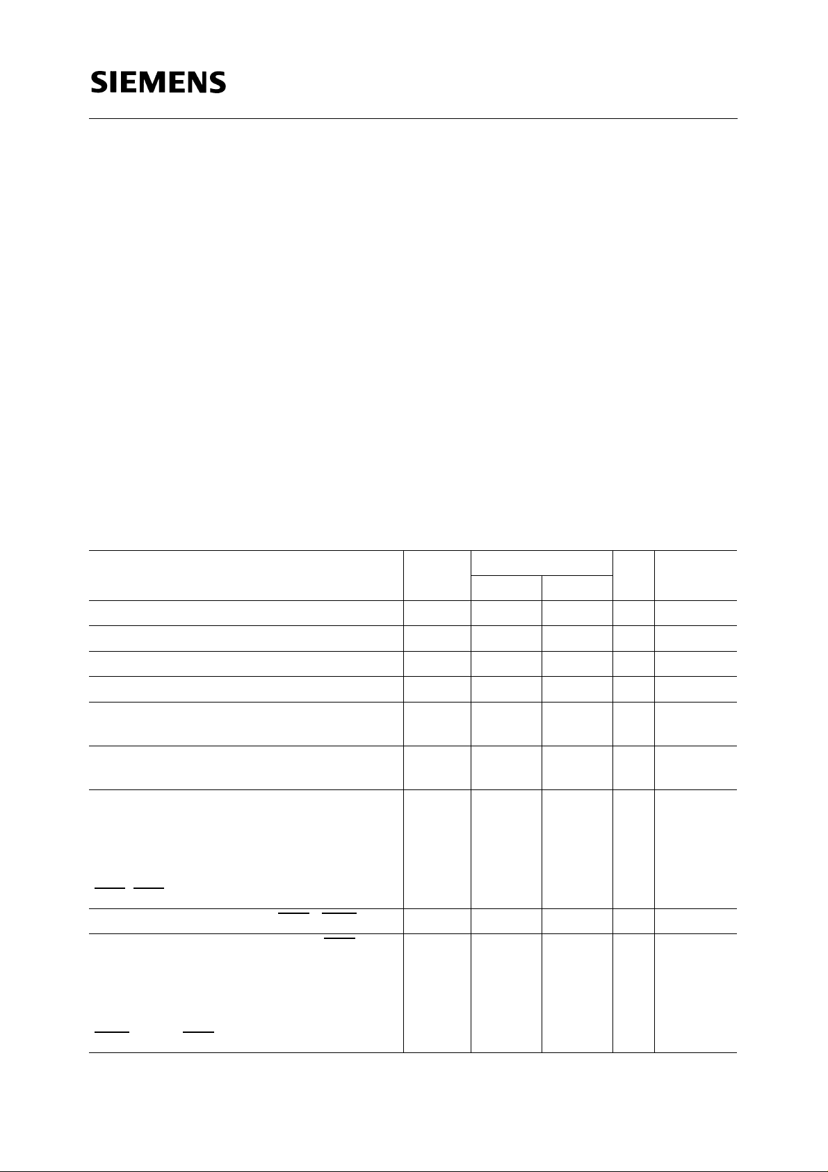
-50 -60 -70
t
RAC
t
CAC
t
AA
t
RC
t
PC
Single + 5 V (± 10 %) supply
•
Low power dissipation
•
RAS
access time 50 60 70 ns
access time 13 15 20 ns
CAS
Access time from address 25 30 35 ns
Read/Write cycle time 90 110 130 ns
Fast page mode cycle time 35 40 45 ns
max. 550 active mW (-50 version)
max. 495 active mW (-60 version)
max. 440 active mW (-70 version)
11 mW standby (TTL)
5.5. mW standby (MOS)
Output unlatched at cycle end allows two-dimensional chip selection
•
Read, write, read-modify-write, CAS-before-RAS refresh, RAS-only refresh, hidden refresh
•
and self refresh
Fast page mode capability
•
2 CAS / 1 WE
•
All inputs, outputs and clocks fully TTL-compatible
•
4096 refresh cycles/64 ms
•
Plastic Package: P-SOJ-42-1 400 mil
•
Semiconductor Group 1 1.96
HYB 5116160BSJ-50/-60/-70
1M x 16-DRAM
The HYB 5116160BSJ is a 16 MBit dynamic RAM organized as 1 048 576 words by 16 bits. The
HYB 5116160BSJ utilizes a submicron CMOS silicon gate process technology, as wel l as advanced
circuit techniques to provide wide operating margins, both internally and for the system user.
Multiplexed address inputs permit the HYB 5116160BSJ to be packaged in a standard SOJ 42
400 mil plastic package. These packages provide hi gh system bit densities and are compatible with
commonly used automatic testing a nd insertion equipment. System-oriented feature s include single
+ 5 V (± 10 %) power supply, direct interfacing with high-perfo rmance logic devi ce families such as
Schottky TTL.
Ordering Information
Type Ordering Code Package Descriptions
HYB 5116160BSJ-50 on request P-SOJ-42-1 400 mil DRAM (access time 50 ns)
HYB 5116160BSJ-60 on request P-SOJ-42-1 400 mil DRAM (access time 60 ns)
HYB 5116160BSJ-70 on request P-SOJ-42-1 400 mil DRAM (access time 70 ns)
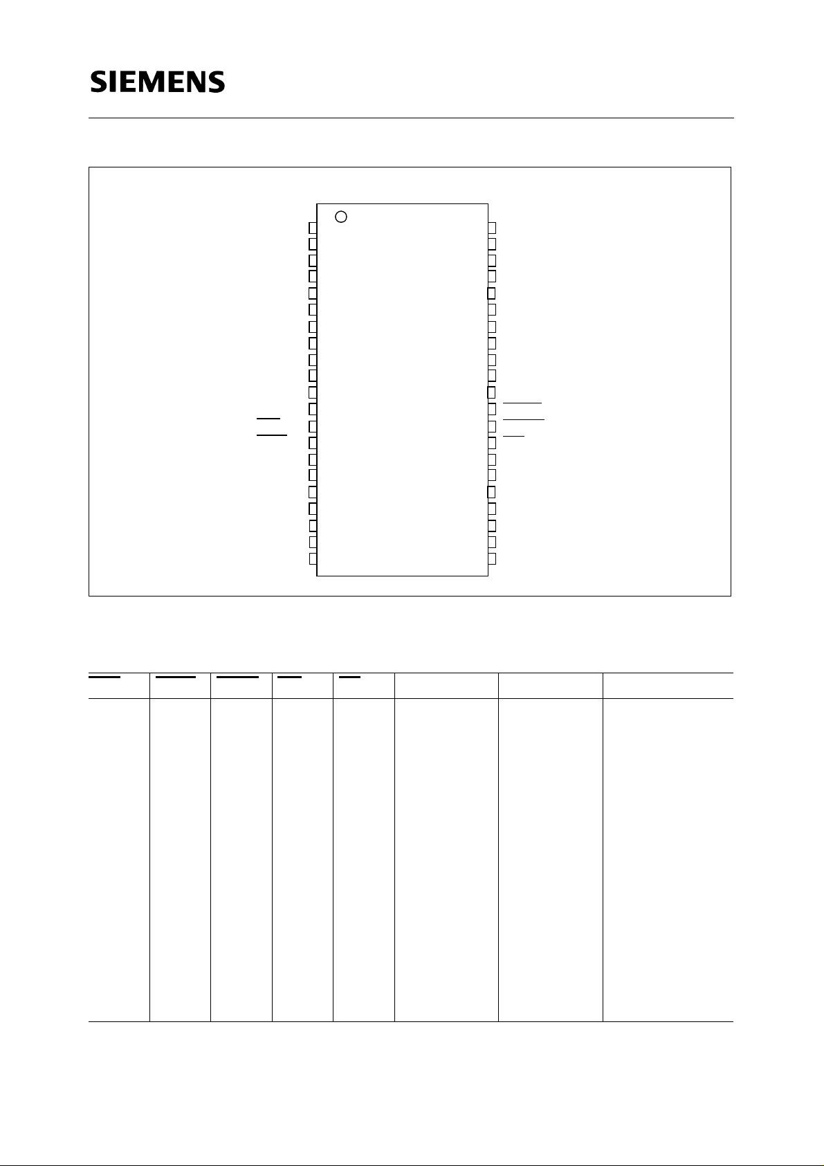
Pin Names
A0 to A11 Row Address Inputs
A0 to A7 Column Addess Inputs
RAS
OE
Row Address Strobe
Output Enable
I/O1-I/O16 Data Input/Output
UCAS
LCAS
WE
V
CC
V
SS
Upper Column Address Strobe
Lower Column Address Strobe
Read/Write Input
Power Supply (+ 5 V)
Ground (0 V)
N.C. not connected
Semiconductor Group 2
P-SOJ-42 (400 mil)
HYB 5116160BSJ-50/-60/-70
1M x 16-DRAM
Pin Configuration
Vcc
I/O1
I/O2
I/O3
I/O4
Vcc
I/O5
I/O6
I/O7
I/O8
N.C.
N.C.
WE
RAS
A11
A10
A0
A1
A2
A3
Vcc
1
2
3
4
5
6
7
8
9
10
11
12
13
14
15
16
17
18
19
20
21
42
41
40
39
38
37
36
35
34
33
32
31
30
29
28
27
26
25
24
23
22
Vss
I/O16
I/O15
I/O14
I/O13
Vss
I/O12
I/O11
I/O10
I/O9
N.C.
LCAS
UCAS
OE
A9
A8
A7
A6
A5
A4
Vss
Truth Table
RAS
H
L
L
L
L
L
L
L
L
LCAS UCAS WE OE I/O1-I/O8 I/O9-I/O16 Operation
H
H
L
H
L
L
H
L
L
H
H
H
L
L
H
L
L
L
H
H
H
H
H
L
L
L
H
H
H
L
L
L
H
H
H
H
High-Z
High-Z
Dout
High-Z
Dout
Din
Don't care
Din
High-Z
High-Z
High-Z
High-Z
Dout
Dout
Don't care
Din
Din
High-Z
Standby
Refresh
Lower byte read
Upper byte read
Word read
Lower byte write
Upper byte write
Word write
NOP
Semiconductor Group 3
WE
HYB 5116160BSJ-50/-60/-70
1M x 16-DRAM
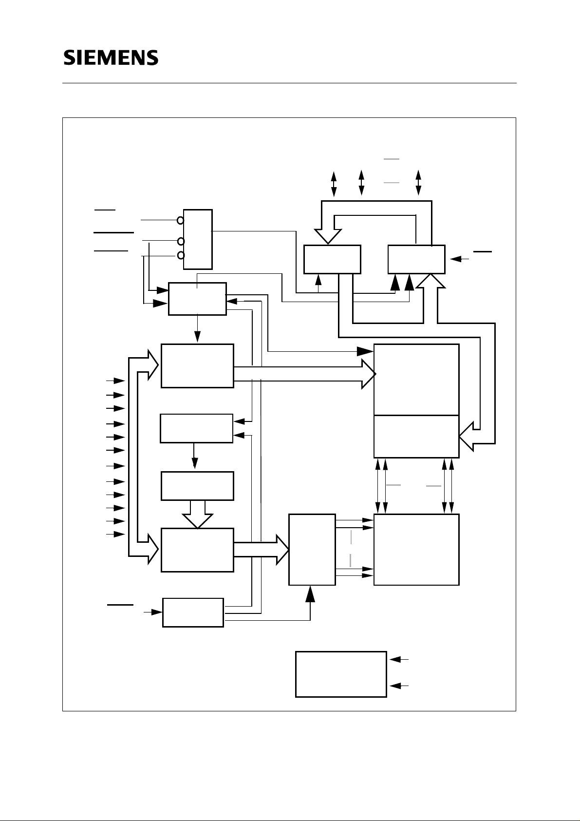
I
I/O1I/O2
/O16
UCAS
LCAS
A0
A1
A2
A3
A4
A5
A6
A7
A8
A9
A10
A11
.
&
.
No. 2 Clock
Generator
Column
8
12 12
Address
Buffer(8)
Refresh
Controller
Refresh
Counter (12)
Row
Address
Buffers(12)
12
Data in
Buffer
Row
Decoder
16
8
4096
Data out
Buffer
16
Column
Decoder
Sense Amplifier
I/O Gating
256
x16
Memory Array
4096x256x16
OE
16
No. 1 Clock
RAS
Block Diagram
Semiconductor Group 4
Generator
Voltage Down
Generator
VCC
VCC (internal)
HYB 5116160BSJ-50/-60/-70
1M x 16-DRAM
Absolute Maximum Ratings
Operating temperature range ............................................................................................0 to 70 °C
Storage temperature range.........................................................................................– 55 to 150 °C
Input/output voltage................................................................................-0.5 to min (Vcc+0.5,7.0) V
Power supply voltage...................................................................................................-1.0V to 7.0 V
Power dissipation.....................................................................................................................1.0 W
Data out current (short circuit)................................................................................................ 50 mA
Note:
Stresses above those listed under “Absolute Maximum Ratings” may cause perm anent dama ge of
the device. Exposure to absolute maximu m rating conditions for extended perio ds may affect device
reliability.
DC Characteristics
= 0 to 70 °C,
T
A
V
SS
= 0 V,
= 5 V ± 10 %, tT = 5 ns
V
CC
Parameter Symbol Limit Values Unit Test
mA
mA
mA
Condition
1)
1)
1)
1)
1)
1)
2) 3) 4)
2) 3) 4)
2) 3) 4)
Input high voltage
Input low voltage
= – 5 mA)
Output high voltage (
Output low voltage (
I
OUT
= 4.2 mA)
I
OUT
Input leakage current,any input
(0 V ≤
≤ Vcc + 0.3V, all other pins = 0 V)
V
IH
Output leakage current
(DO is disabled, 0 V ≤
Average
supply current:
V
CC
≤ Vcc + 0.3V)
V
OUT
-50 ns version
-60 ns version
-70 ns version
V
V
V
V
I
I
I
IH
IL
OH
OL
I(L)
O(L)
CC1
min. max.
2.4 Vcc+0.5 V
– 0.5 0.8 V
2.4 – V
–0.4V
– 10 10 µA
– 10 10 µA
–
–
–
100
90
80
(RAS
, CAS, address cycling, tRC = tRC
supply current (RAS =CAS=
Standby
Average
V
CC
supply current, during RAS-only
V
CC
min.
)
)
V
IH
refresh cycles: -50 ns version
-60 ns version
-70 ns version
(RAS
cycling: CAS =
, tRC = tRC min.)
V
IH
Semiconductor Group 5
I
I
CC2
CC3
–2mA–
–
–
–
100
90
80
mA
mA
mA
2) 4)
2) 4)
2) 4)
HYB 5116160BSJ-50/-60/-70
1M x 16-DRAM
DC Characteristics
= 0 to 70 °C,
T
A
V
SS
(cont’d)
= 0 V,
= 5 V ± 10 %, tT = 5 ns
V
CC
Parameter Symbol Limit Values Unit Test
mA
mA
mA
mA
mA
mA
Condition
2) 3) 4)
2) 3) 4)
2) 3) 4)
1)
2) 4)
2) 4)
2) 4)
supply current,
Average
V
CC
during fast page mode: -50 ns version
-60 ns version
-70 ns version
(RAS
=
, CAS, address cycling, tPC = t
V
Standby
(RAS
= CAS =
Average
IL
supply current
V
CC
– 0.2 V)
V
CC
supply current, during CAS-
V
CC
PC
before-RAS refresh mode: -50 ns version
-60 ns version
-70 ns version
(RAS
, CAS cycling, tRC = t
RC
min.)
Average Self Refresh Current
min.
min. max.
I
CC4
–
–
–
40
35
30
)
I
I
I
CC5
CC6
CC7
–1mA
–
–
–
100
90
80
_1mA
(CBR cycle with tRAS>TRASSmin., CAS held low,
WE
=Vcc-0.2V, Address and Din=Vcc-0.2V or 0.2V)
Capacitance
= 0 to 70 °C,
T
A
= 5 V ± 10 %, f = 1 MHz
V
CC
Parameter Symbol Limit Values Unit
min. max.
Input capacitance (A0 to A11)
Input capacitance (RAS
, UCAS, LCAS, WE, OE)
I/O capacitance (I/O1-I/O16)
C
I1
C
I2
C
IO
–5pF
–7pF
–7pF
Semiconductor Group 6
HYB 5116160BSJ-50/-60/-70
1M x 16-DRAM
AC Characteristics
= 0 to 70 °C,
T
A
5)6)
= 5 V ± 10 %, tT = 5 ns
V
CC
Parameter
common parameters
Random read or write cycle time t
RAS
precharge time t
pulse width t
RAS
CAS
pulse width t
Row address setup time t
Row address hold time t
Column address setup time t
Column address hold time t
to CAS delay time t
RAS
RAS
to column address delay
time
Symbol
RC
RP
RAS
CAS
ASR
RAH
ASC
CAH
RCD
t
RAD
Limit Values
Unit Note
-50 -60 -70
min. max. min. max. min. max.
90 – 110 – 130 – ns
30 – 40 – 50 – ns
50 10k 60 10k 70 10k ns
13 10k 15 10k 20 10k ns
0–0–0–ns
8–10–10–ns
0–0–0–ns
10 – 15 – 15 – ns
18 37 20 45 20 50
13 25 15 30 15 35 ns
16F
hold time t
RAS
CAS
hold time t
to RAS precharge time t
CAS
Transition time (rise and fall) t
Refresh period t
Read Cycle
Access time from RAS
Access time from CAS
Access time from column address t
access time t
OE
Column address to RAS
lead time t
Read command setup time t
Read command hold time t
Read command hold time
referenced to RAS
CAS
to output in low-Z t
Output buffer turn-off delay t
t
t
t
RSH
CSH
CRP
T
REF
RAC
CAC
AA
OEA
RAL
RCS
RCH
RRH
CLZ
OFF
13 15 – 20 – ns
50 60 – 70 – ns
5–5–5–ns
350350350ns7
–64–64–64ms
–50–60–70ns8, 9
–13–15–20ns8, 9
–25–30–35ns8,10
–13–15–20ns
25 – 30 – 35 – ns
0–0–0–ns
0–0–0–ns11
0–0–0–ns11
0–0–0–ns8
013015020ns12
Semiconductor Group 7
HYB 5116160BSJ-50/-60/-70
1M x 16-DRAM
AC Characteristics
= 0 to 70 °C,
T
A
V
CC
(cont’d)
= 5 V ± 10 %, tT = 5 ns
5)6)
Parameter
Output buffer turn-off delay from
OE
Data to OE
high to data delay t
CAS
OE
high to data delay t
low delay t
Write Cycle
Write command hold time t
Write command pulse width t
Write command setup time t
Write command to RAS
Write command to CAS
lead time t
lead time t
Data setup time t
Data hold time t
Data to CAS
low delay t
Symbol
t
OEZ
DZO
CDD
ODD
WCH
WP
WCS
RWL
CWL
DS
DH
DZC
16F
Limit Values
Unit Note
-50 -60 -70
min. max. min. max. min. max.
013015020ns12
0–0–0–ns13
13 – 15 – 20 – ns 14
13 – 15 – 20 – ns 14
8–10–10–ns
8–10–10–ns
0–0–0–ns15
13 – 15 – 20 – ns
13 – 15 – 20 – ns
0–0–0–ns16
10 – 10 – 15 – ns 16
0–0–0–ns13
Read-Modify-Write Cycle
Read-write cycle time t
to WE delay time t
RAS
CAS
to WE delay time t
Column address to WE
OE
command hold time t
delay time t
RWC
RWD
CWD
AWD
OEH
126 – 150 – 180 – ns
68 – 80 – 95 – ns 15
31 – 35 – 45 – ns 15
43 – 50 – 60 – ns 15
13 – 15 – 20 – ns
Fast Page Mode Cycle
Fast page mode cycle time t
CAS
precharge time t
Access time from CAS
RAS
pulse width t
precharge to RAS Delay t
CAS
precharge t
PC
CP
CPA
RAS
RHPC
35 – 40 – 45 – ns
10 – 10 – 10 – ns
–30–35–40ns7
50 200k 60 200k 70 200k ns
30 – 35 – 40 – ns
Semiconductor Group 8
 Loading...