

Page 1
Service manual Level 3
for
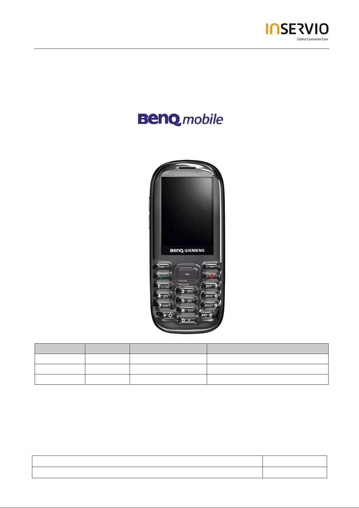
E71
Release Date Department Notes to change
R 1.0 22.09.2006 ISC S CES New document
Technical Documentation Release 1.0
TD_Repair_L3 _Theory of Operation_E71_R1.0.pdf Page 1 of 35
Created by inservio GmbH for BenQ mobile GmbH & Co. OHG - Company Confidential2006©inservio
Page 2

Table of Content
1 Introduction ...............................................................................................................................4
1.1 PURPOSE...............................................................................................................................4
1.2 SCOPE...................................................................................................................................4
1.3 TERMS AND ABBREVIATIONS ...................................................................................................4
2 List of available level 3 parts....................................................................................................5
3 Required Equipment for Level 3 ..............................................................................................6
4 Required Software for Level 3..................................................................................................6
5 PCB Main Board Overview .......................................................................................................7
6 Radio Part ..................................................................................................................................8
6.1 BLOCK DIAGRAM RF PART.......................................................................................................9
6.2 POWER SUPPLY RF-PART ......................................................................................................9
6.3 FREQUENCY GENERATION -...................................................................................................10
6.4 RECEIVER ............................................................................................................................11
6.5 TRANSMITTER.......................................................................................................................12
6.6 BRIGHT IC OVERVIEW...........................................................................................................14
6.7 ANTENNA SWITCH (ELECTRICAL/MECHANICAL) .......................................................................16
6.8 TRANSMITTER: POWER AMPLIFIER ........................................................................................17
7 Logic / Control.........................................................................................................................18
7.1 OVERVIEW HARDWARE STRUCTURE E71...............................................................................18
7.2 SGOLD2 .............................................................................................................................19
7.3 EXTERNAL MEMORY..............................................................................................................22
7.3.1 FLASH..........................................................................................................................22
7.3.2 Low Power SDRAM......................................................................................................22
7.4 MEMORY CARD ....................................................................................................................22
7.5 SIM......................................................................................................................................23
7.6 FM-RADIO............................................................................................................................23
7.7 SERVICE INDICATION LED.....................................................................................................23
7.8 VIBRATION MOTOR ...............................................................................................................23
8 Display......................................................................................................................................24
9 Camera .....................................................................................................................................24
Technical Documentation Release 1.0
TD_Repair_L3 _Theory of Operation_E71_R1.0.pdf Page 2 of 35
Created by inservio GmbH for BenQ mobile GmbH & Co. OHG - Company Confidential2006©inservio
Page 3

10 Bluetooth..................................................................................................................................25
11 Power Supply...........................................................................................................................26
11.1 PMU MOZART BOOST+ / TWIGO4 BOOST+............................................................................26
11.2 BATTERY..............................................................................................................................26
11.3 CHARGING CONCEPT............................................................................................................26
12 MMI ...........................................................................................................................................28
12.1 KEYBOARD...........................................................................................................................28
12.2 SIDE KEYS:...........................................................................................................................28
12.3 KEYPAD ILLUMINATION:.........................................................................................................28
13 Interfaces .................................................................................................................................28
13.1 MICROPHONE (XG1901).......................................................................................................28
13.2 BATTERY (X1400) ................................................................................................................29
13.3 VIBRATION MOTOR (XG2100)...............................................................................................29
13.4 INTERFACE SIM MODULE WITH ESD PROTECTION .................................................................30
13.5 NANO IO CONNECTOR WITH ESD PROTECTION .....................................................................31
13.6 DISPLAY CONNECTOR...........................................................................................................33
13.7 MMI CONNECTOR.................................................................................................................34
13.8 CAMERA CONNECTOR...........................................................................................................35
14 E71 Diagram Sets....................................................................................................................35
Technical Documentation Release 1.0
TD_Repair_L3 _Theory of Operation_E71_R1.0.pdf Page 3 of 35
Created by inservio GmbH for BenQ mobile GmbH & Co. OHG - Company Confidential2006©inservio
Page 4

1 Introduction
1.1 Purpose
This Service Repair Documentation is intended to carry out repairs on BenQ repair level 3.
1.2 Scope
This document is the reference document for all BenQ authorised Service Partners which are
released to repair BenQ Siemens mobile phones up to level 3.
1.3 Terms and Abbreviations
Technical Documentation Release 1.0
TD_Repair_L3 _Theory of Operation_E71_R1.0.pdf Page 4 of 35
Created by inservio GmbH for BenQ mobile GmbH & Co. OHG - Company Confidential2006©inservio
Page 5
2 List of available level 3 parts
(according to Component Matrix V1.13 - check C-market for updates)
Product ID OrderNumber DescriptionCM
E71 D1000 L50610-G6282-D670 IC SGOLD2PMB8876X2.1J11
E71 D1300 L50645-J4683-Y23 IC ASIC TWIGO4+BOOST MOZART-BOOST+BGA196
E71 D1800 L50620-L6172-D670 IC TELEC TEA5761UK
E71 D5100 L50610-U6122-D670 IC BLUETOOTHBRF6150PB-FREE
E71 D5930 L50645-K280-Y303 IC FEM HITACHIGSM90018001900 (FEM -Type 5)
E71 D5932 L50620-L6175-D670 IC TRANCEIVER Bright 6PL
E71 D5933 L50651-Z200-2A91 IC MODUL PA PF09039B (PA-Type 8)PBFree
E71 L1301 L50651-F5103-M1 Coil 10U (Co-Type 9)
E71 L1302 L36151-F5103-M7 Coil 10U (Co-Type 2)
E71 N3500 L50610-C6153-D670 IC V-REG 2.9V (Vr-Type 2)PBFree
E71 N4800 L50610-C6153-D670 IC V-REG 2.9V (Vr-Type 2)PBFree
E71 R1347 L36120-F4223-H Resistor TEMP22K (Res-Type 7)
E71 R5967 L36120-F4223-H Resistor TEMP22K (Res-Type 7)
E71 V1302 L36840-D5076-D670 Diode SOD323 (Di-Type 7)
E71 V1305 L50630-C1127-D670 Transistor FDMA1027P (Tra-Type 19)
E71 V1376 L50630-C1152-D670 Transistor FDMA3N109 (Tra-Type 18)
E71 V1400 L50640-D70-D670 Diode BAV99T (Di-Type 9)
E71 V2100 L50640-D5084-D670 Diode RB548W (Di-Type 8)
E71 V2300 L36840-C4061-D670 Transistor BC847BSBC846S (Tra-Type 10)
E71 V2302 L50640-C2131-D670 Transistor NPN+R1 R2 PDTC (Tra-Type 20)
E71 V2405 L50640-L2110-D670 LED GREEN SIDE-SHOOTER
E71 V2801 L36840-C4061-D670 Transistor BC847BSBC846S (Tra-Type 10)
E71 V2802 L50640-C2131-D670 Transistor NPN+R1 R2 PDTC (Tra-Type 20)
E71 X1400 L50634-Z97-C467 CONNECTOR BATTERY 3-POLX85
E71 X1504 L50634-Z93-C364 IO-JACK NANO 12-POL
E71 X1604 L50634-Z97-C406 CONNECTOR SIM CARD READER R65 (B)
E71 X2200 L50634-Z97-C457 CONNECTOR B2B 20-POL MALE
E71 X2705 L50634-Z97-C363 CONNECTOR BOARD TO BOARD 14-POL.X75
E71 X3500 L50634-Z97-C516 CONNECTOR HYDRA-CAMERA-SOCKET
E71 X4081 L50634-Z97-C382 CONNECTOR COAX SOCKET SWITCH ED2
E71 X4899 L50634-Z97-C448 CONNECTOR CARD READER TRANSFLASHHINGE
E71 Z1001 L50645-F102-Y40 QUARZ32,768KHZ (Q-Type 4)
E71 Z1501 L50620-U6067-D670 FILTER EMI (Fi-Type 8)PBFree
E71 Z1601 L50620-U6029-D670 FILTER EMI (Fi-Type 6)PBFree
E71 Z4801 L50620-U6030-D670 FILTER EMI (Fi-Type 10)PBFree
E71 Z5100 L50645-K280-Y330 FILTER BPBLUETOOTH
E71 Z5930 L50645-F260-Y37 QUARZ26MHZ (Q-Type 10)
Technical Documentation Release 1.0
TD_Repair_L3 _Theory of Operation_E71_R1.0.pdf Page 5 of 35
Created by inservio GmbH for BenQ mobile GmbH & Co. OHG - Company Confidential2006©inservio
Page 6

3 Required Equipment for Level 3
GSM-Tester (CMU200 or 4400S incl. Options)
PC-incl. Monitor, Keyboard and Mouse
Bootadapter 2000/2002 (L36880-N9241-A200)
Adapter cable for Bootadapter due to
Troubleshooting Frame E71 (F30032-P)
Power Supply
Spectrum Analyser
Active RF-Probe incl. Power Supply
Oscilloscope incl. Probe
RF-Connector (N<>SMA(f))
Power Supply Cables
Dongle (F30032-P28-A1) if USB-Dongle is used a special driver for NT is required
BGA Soldering equipment
Reference: Equipment recommendation V2.0
(downloadable from the technical support page)
new Lumberg connector (F30032-P226-A2)
4 Required Software for Level 3
Windows XP
X-Focus version 2.04 or higher
GRT Version 4.04 or higher
Internet unblocking solution (JPICS)
Technical Documentation Release 1.0
TD_Repair_L3 _Theory of Operation_E71_R1.0.pdf Page 6 of 35
Created by inservio GmbH for BenQ mobile GmbH & Co. OHG - Company Confidential2006©inservio
Page 7

5 PCB Main Board Overview
PCB Main Board Top Side
32,768 kHz Oscillator
IC SGOLD2
IC SGOLD2
IC FLASHSDRAM
IC Flash SDRAM
PCB Main Board Back Side
IC TELEC TEA5761UK
CONNECTOR B2B 20-POL MALE
IC BLUETOOTHBRF6150
IC TRANCEIVER
26 MHz Oscillator
CONNECTOR BTOB 14-POL
IC FEM HITACHI
IC MODUL PA
Technical Documentation Release 1.0
TD_Repair_L3 _Theory of Operation_E71_R1.0.pdf Page 7 of 35
IC ASIC
Created by inservio GmbH for BenQ mobile GmbH & Co. OHG - Company Confidential2006©inservio
CONNECTOR CARD READER TRANSFLASH
CONNECTOR CAMERA-SOCKET
Page 8

6 Radio Part
The radio part realizes the conversion of the GMSK/8PSK RF-signals from the antenna to
the base-band and vice versa. In the receiving direction, the signals are split in the I- and Qcomponent and led to the A/D-converter of the logic part. In the transmission direction, the
GMSK/8PSK signals are generated digitally by the baseband section. After D/A conversion
the analogue signals are fed into an IQ modulator and up-converted to radio frequencies by
the polar loop system. After that the signals are amplified in the power amplifier.
Transmitter and Receiver are never active at the same time. Therefore full duplex operation
is not possible. However the monitoring band (monitoring timeslot) in the TDMA-frame can
be chosen independently of the receiving respectively the transmitting band (RX- and TX
timeslot of the band).
The RF part is dimensioned for quad band operation in the frequency ranges GSM850/
EGSM900/DCS1800/ PCS1900 supporting EGPRS functionality up to multi class 12.
E71 supports EGSM900/DCS1800/PCS1900.
The RF-circuit consists of the following components:
• Renesas Bright 6PLA chip set
PLL for integrated local oscillator LO including loop filter
Fully integrated TxVCO and TX-PLL including loop filter
Direct conversion receiver including LNA, DC-mixer, channel filtering and PGC-
amplifier
Active part of 26 MHz reference oscillator and varicap
• Integrated Polar Loop, phase and amplitude control of transmitted output power
• Renesas transmit PA PF09036B
• Hitachi Front-end Module
HWXQ521 including RX-/TX-switch and EGSM900 / DCS1800 / PCS 1900 receiver
SAW-filters
or
HWXQ522 including RX-/TX-switch and GSM850 / DCS1800 / PCS 1900 receiver
SAW-filters
or
HWXR591 including RX-/TX-switch and GSM850 / EGSM900 / DCS1800 / PCS
1900 receiver SAW-filters
Technical Documentation Release 1.0
TD_Repair_L3 _Theory of Operation_E71_R1.0.pdf Page 8 of 35
Created by inservio GmbH for BenQ mobile GmbH & Co. OHG - Company Confidential2006©inservio
Page 9

6.1 Block diagram RF part
6.2 Power Supply RF-Part
The voltage regulator for the RF-part is located inside the ASIC D1300. It generates the
required 2,8V “RF-Voltages” named VDD_RF1 and VDD_RF2. The voltage regulator is
activated as well as deactivated via VCXOEN_UC
The temporary deactivation is used to extend the stand by time.
okay
Technical Documentation Release 1.0
(Functional K19) provided by the SGOLD2.
TD_Repair_L3 _Theory of Operation_E71_R1.0.pdf Page 9 of 35
Created by inservio GmbH for BenQ mobile GmbH & Co. OHG - Company Confidential2006©inservio
Page 10

6.3 Frequency generation -
Discrete 26MHz VCXO reference oscillator
The 26 MHz signal is created by an integrated VCXO. A Colpitts oscillator is used with a
post-connected buffer stage. The active part and the varicaps are realized within the Bright.
The integrated varicap is split up into different smaller varicaps to adjust the center
frequency of the VCXO with different crystal vendors and mass production variation. For
temperature measurements of the VCXO an external temperature sensor is used. The
frequency of the reference oscillator can be fine tuned by the SGOLD2 via a filtered PNM
modulated AFC signal(RF_AFC). Three active buffer stages are included in Bright 6PLA to
provide clock signals for the baseband IC, Bluetooth and the PMU ASIC.
The required voltage VDD_RF1/VDD_RF2 is provided by the ASCI D1300
Waveform of the AFC_PNM signal from SGOLD2 to Oscillator
Signalform
SGOLD2
1 2 3
RF_AFC
1
R1
AFC_PNM
2
R2
R3
3
C1
C2
C3
GND
GND
GND
Technical Documentation Release 1.0
TD_Repair_L3 _Theory of Operation_E71_R1.0.pdf Page 10 of 35
Created by inservio GmbH for BenQ mobile GmbH & Co. OHG - Company Confidential2006©inservio
Page 11

Synthesizer: LO
The local oscillator (LO) consists of a PLL and VCO inside Bright D5932 and an integrated
loop filter. The VCO includes a calibration mechanism which is triggered automatically
before each synthesizer programming.
RF PLL
The RF-PLL is a fractional-N-PLL. The RF frequency is calculated within Bright D5932 from
the channel frequency information which is programmed into Bright D5932. In TX mode
there is the possibility to correct the RF frequency by a few 100Hz to correct for TX
frequency errors. The reference frequency of the PLL is 26MHz. The PLL is controlled by
the internal state machine.
RFVCO (LO)
The first local oscillator is needed to generate frequencies which enable the transceiver IC
to demodulate the receiver signal and to perform the channel selection in the TX part. The
VCO module is switched on with the signal PLLON.The full oscillation range is divided into
256 sub bands and covers 3476 to 4026MHz. The choice of the appropriate band and the
complete operation is controlled internally by the Bright state machine.
TX IF Generation
The TX IF signal is derived from the RFVCO signal by a divider. Four different divider ratios
(40, 44, 48, and 52) can be selected by programming. As with the channel frequency also
the RFVCO frequency changes the TX IF is no longer a fixed frequency but changes also
depending on the divider ratio in the range from 68.4MHz to 100.6MHz.
6.4 Receiver
Receiver: Filter to Demodulator
The Bright D5932 incorporates four RF LNAs for GSM850, EGSM900, DCS1800 and
PCS1900 operation followed by direct conversion mixers which are IQ demodulators. The
LNA/mixer can be switched in normal-, low- and lower-gain and high isolation mode. For the
“normal gain“ state the mixers are optimised in terms of conversion gain and noise figure, in
the “low gain“ state the mixers are optimised for large-signal behaviour for operation at a
high input power levels. The "lower gain mode" reduces the RF-level by activating
differential impedance in front of the LNA to improve the large signal performance.
Triple band operation (GSM850, DCS1800 and PCS1900) is also possible because both
low band LNA’s can both operate in the GSM850 and EGSM900 bands. The frequency
bands are determined by the front-end module D5930 which is used and by the synthesizer
programming.
Technical Documentation Release 1.0
TD_Repair_L3 _Theory of Operation_E71_R1.0.pdf Page 11 of 35
Created by inservio GmbH for BenQ mobile GmbH & Co. OHG - Company Confidential2006©inservio
Page 12

Furthermore the IC includes a programmable gain baseband amplifier PGA (90dB control
range, 2dB steps) with automatic DC offset calibration. The channel filtering is realized
inside the chip with a four stage baseband filter for both IQ chains. Two capacitors which
are part of the first passive RC-filters are now integrated and calibrated during the
initialization sequence of B6PLA. The second, third and fourth filters are active filters and
are fully integrated. The distributed channel filter is necessary to suppress adjacent channel
and inband-blocking interferer to avoid any compression in each amplifier stage.
The down converted IQ signals are fed into the A/D converters inside the SGOLD2. By a
special algorithm the level of the IQ signals is kept constant on a defined level by varying
the PGA gain and selecting the appropriate LNA gains.
Filter
LNA
Demodulator
PGC
D5930 Bright(D5932)
The required voltage VDD_RF1/VDD_RF2 is provided by the ASIC D1300
6.5 Transmitter
Polar Loop
The generation of the modulated RF signal in Bright is based on the principle of the polar
loop architecture. The IQ signals generated by the SGOLD2 baseband are modulated to the
transmit IF of 68.4MHz to 100.6MHz by an IQ modulator. The required IF is generated by
dividing the RFVCO signal.
As in a conventional up-conversion loop the IF signal is up-converted to the transmit
frequency. There-fore a down-converter and a phase detector are used in order to compare
the IF signal to the down-converted transmit signal. This loop is called PM loop and is used
for GMSK operation.
In 8PSK mode the transmit IF-signal is split into PM and AM components. A second loop is
then used to control the AM components. Therefore an AM detector is implemented which
compares the transmit IF-signal and the down-converted transmit signal. The AM loop is
also used for power ramping. Inside the AM loop there are two analogue gain controlled
amplifiers. These are used for setting the output power level and to keep the loop bandwidth
constant. External attenuators are required in the feedback paths from PA to Bright to adjust
the feedback level to PA’s from different suppliers.
The separated AM and PM components of an 8PSK signal are finally fit together inside the
PA. The PA is driven by the TXVCO signals containing the PM components. The AM
component is added by an amplitude control input pin, which controls the supply voltage of
the RF transistors and therefore the PA output power level.
Technical Documentation Release 1.0
TD_Repair_L3 _Theory of Operation_E71_R1.0.pdf Page 12 of 35
Created by inservio GmbH for BenQ mobile GmbH & Co. OHG - Company Confidential2006©inservio
Page 13

All loop filters for PM and AM loops are fully integrated within Bright. To achieve a good
output modulation spectrum it is necessary that the bandwidths of the PM loop and the AM
loop are quite well adjusted to their target bandwidth. For the PM loop there is an automatic
calibration mechanism within B6PLA running prior to each TX slot. The AM loop bandwidth
is calibrated only one time in the factory.
TxVCO
The TxVCO is integrated inside Bright. It consists of 256 VCO bands operating in the
frequency range 1648MHz to 1910MHz. The signal for the low bands GSM850 and
EGSM900 is generated by a 1/2 divider. Two independent output buffers, one for each
band, deliver the output signal to the PA module input. The choice of the appropriate VCO
band is done automatically and controlled by the internal state machine.
Modulator
Filter
PD
TxVCO
Bright(D5932)
The required voltage VDD_RF1/VDD_RF2 is provided by the ASIC D1300
Technical Documentation Release 1.0
TD_Repair_L3 _Theory of Operation_E71_R1.0.pdf Page 13 of 35
Created by inservio GmbH for BenQ mobile GmbH & Co. OHG - Company Confidential2006©inservio
Page 14

6.6 Bright IC Overview
BRIGHT 6PL
IC Overview
Technical Documentation Release 1.0
TD_Repair_L3 _Theory of Operation_E71_R1.0.pdf Page 14 of 35
Created by inservio GmbH for BenQ mobile GmbH & Co. OHG - Company Confidential2006©inservio
Page 15
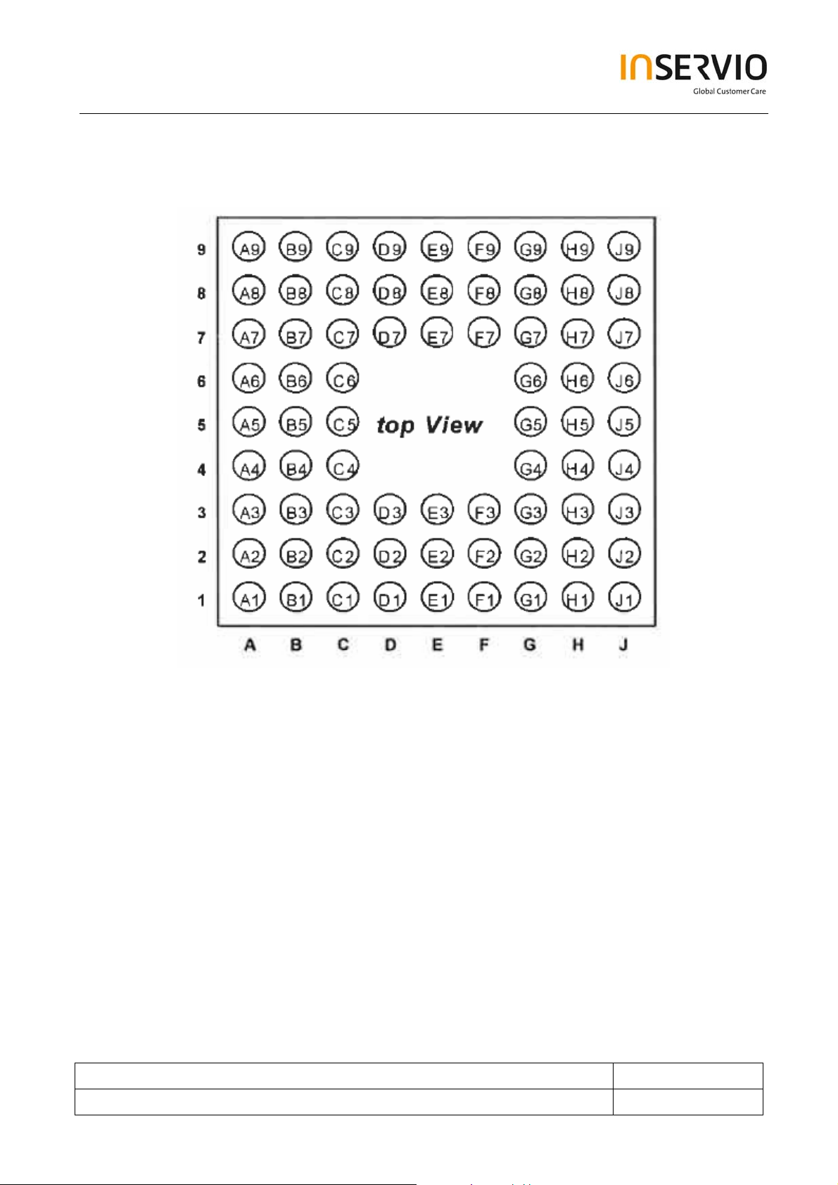
IC top view (ball overview)
Technical Documentation Release 1.0
TD_Repair_L3 _Theory of Operation_E71_R1.0.pdf Page 15 of 35
Created by inservio GmbH for BenQ mobile GmbH & Co. OHG - Company Confidential2006©inservio
Page 16

6.7 Antenna switch (electrical/mechanical)
Internal/External <> Receiver/Transmitter
The E71 mobile have two antenna switches.
a) The mechanical antenna switch for the differentiation between the internal and
external antenna which is used
b) The electrical antenna switch, for the differentiation between the receiving and
transmitting signals.
To activate the correct tx pathes of this diplexer, the SGOLD2 signals FEMC1 and FEMC2
are required.
Internal/External antenna switch
The electrical antenna switch
only for RF adjustments on the board.
Technical Documentation Release 1.0
TD_Repair_L3 _Theory of Operation_E71_R1.0.pdf Page 16 of 35
Created by inservio GmbH for BenQ mobile GmbH & Co. OHG - Company Confidential2006©inservio
Page 17

okay
6.8 Transmitter: Power Amplifier
The power amplifier is a PA module matched to 50 Ω at all signal ports. It contains a two
stage amplifier for the GSM850/EGSM900 and a three stage amplifier for
DCS1800/PCS1900 operation. It is possible to control the output power level of both bands
via one VRAMP port. The appropriate amplifier chain is activated by a logic signal, which is
provided by Bright (TXBAND). The module is switched on by a control signal generated by
the Bright internal state machine (TX_ON). The RF transistor bias voltage is generated
inside the PA module. The PA module consists also of two additional directional couplers to
provide the needed RF feedback signal for the AM control in 8PSK mode.
In GMSK operation the output power is directly controlled by a control voltage coming from
SGOLD2. This voltage is fed through Bright and connected to the PA module (VRAMP).
The 3GPP specification can be fulfilled without power sensing or any type of feedback.
In 8PSK operation the AM loop controls the output power level. Therefore the same
SGOLD2 signal is used but connected to the variable gain amplifiers inside Bright. The AM
control voltage finally controls the PA module (VRAMP). All switching between GMSK and
8PSK modes is controlled by the Bright internal state machine.
The required voltage BATT+ is provided by the battery.
okay
Technical Documentation Release 1.0
TD_Repair_L3 _Theory of Operation_E71_R1.0.pdf Page 17 of 35
Created by inservio GmbH for BenQ mobile GmbH & Co. OHG - Company Confidential2006©inservio
Page 18

7 Logic / Control
7.1 Overview Hardware Structure E71
okay
Technical Documentation Release 1.0
TD_Repair_L3 _Theory of Operation_E71_R1.0.pdf Page 18 of 35
Created by inservio GmbH for BenQ mobile GmbH & Co. OHG - Company Confidential2006©inservio
Page 19

7.2 SGOLD2
Baseband Processor SGOLD2 Features
Supported Standards
• EGPRS class 12 MCS 1..9
• GSM speech FR, HR, EFR and AMR-NB
• GSM data 2.4kbit/s, 4.8kbit/s, 9.6kbits, and 14.4kbit/s
• HSCSD class 10
• GPRS class 12 CS 1..4
Processing cores
• ARM926EJ-S 32 bit processor core with operating frequency up to 208 MHz for
controller functions. The ARM926EJ-S includes an MMU, and the Jazelle Java
extension for Java acceleration.
• TEAKLite® DSP core with operating frequency 138.67 MHz.
ARM-Memory
TEAKLite®-Memory (word: 16bit)
Shared Memory Blocks (word: 16bit)
Controller Bus System
TEAKLite® Bus System
Clock System
The clock system allows widely independent selection of frequencies for the essential
parts of the S-GOLDliteTM. Thus power consumption and performance can be
optimized for each application.
Technical Documentation Release 1.0
TD_Repair_L3 _Theory of Operation_E71_R1.0.pdf Page 19 of 35
Created by inservio GmbH for BenQ mobile GmbH & Co. OHG - Company Confidential2006©inservio
Page 20

Functional Hardware blocks
• CPU and DSP Timers
• Programmable PLL with additional phase shifters for system clock generation
• GSM Timer Module that off-loads the CPU from radio channel timing
• GMSK Modulator according to GSM-standard 05.04 (5/2000)
– GMSK Modulator: gauss-filter with B*T=0.3
• Hardware accelerators for equalizer and channel decoding
• A5/1, A5/2, A5/3 Cipher Unit
(A5/3 added in S-GOLDliteTM V1.1)
• GEA1, GEA2, GEA3 Cipher Unit to support GPRS data transmission
(GEA3 added in S-GOLDliteTM V1.1)
• Advanced static and dynamic power management features including TDMA-Frame
synchronous low-power mode and enhanced CPU modes (idle and sleep modes)
• Incremental Redundancy Memory for EDGE class 12 support
• GMSK / 8-PSK Modulator according to GSM-standard 05.04 (5/2000)
– GMSK Modulator: gauss-filter with B*T=0.3
– EDGE Modulator: 8PSK-modulation with linearised GMSK-pulse-filter
• MOVE coprocessor performing motion estimation for video encoding algorithms
(H.263, MPEG-4)
Signal Processing Firmware Support
• FR, HR, EFR, and AMR
• data transmission channel codecs for 2.4, 4.8, 9.6 and 14.4 kbit/s
• HSCDS class 10 support
• GPRS class 12 support with coding schemes CS1..4
• Support for Handsfree, side- and signaling tone generation
• MMS-support
• EGPRS class 12 with modulation and coding schemes MCS1..9 (Release 5 compliant)
• Polyphonic ringer for up to 64 voices at sampling rates up to 48kHz
• 64 voices midi (pseudo) stereo
• enhanced audio visualization
• voice control
Technical Documentation Release 1.0
TD_Repair_L3 _Theory of Operation_E71_R1.0.pdf Page 20 of 35
Created by inservio GmbH for BenQ mobile GmbH & Co. OHG - Company Confidential2006©inservio
Page 21

Interfaces and Features
• Keypad Interface for scanning keypads up to 8 rows and 8 columns
• Pulse Number Modulation output for Automatic Frequency Correction (AFC)
• Serial RF Control Interface; support of direct conversion RF
• 2 USARTs
• IrDA Controller
• 1 Serial Synchronous SPI compatible interfaces in the controller domain
• 1 Serial Synchronous SPI compatible interface in the TEAKLite® domain
• I2C-bus interface
• 2 bidirectional and one unidirectional I2S interface accessible from the TEAKLite®
• USB V1.1 mini host interface
• IEEE 1149.1 compliant JTAG port for Boundary Scan and debug
• ISO 7816 compatible SIM card interface
• Enhanced digital baseband filters, including analog prefilters a/d converters.
• Digital and analog audio filters including wideband audio capable digital-to-analog and
analog-to-digital converters.
• Audio front-end will be accessible from MCU (via shared memory) and the TEAKLite®
(i.e. voice recognition and echo cancellation can run on TEAKLite®)
• Hifi Stereo voiceband with CD-Quality
• Separate analog-to-digital converter for various general purpose measurements like
battery voltage, battery, VCXO and environmental temperature, battery technology,
transmission power, offset, onchip temperature, etc.
• Ringer support for highly oversampled PDM/PWM input signals
• Differential VMIC generation
• RF power ramping functions
• DAI Interface according to GSM 11.10 is implemented via dedicated I2S mode
• 26 MHz master clock input
• External memory interface:
• Port logic for external port signals
• Comprehensive static and dynamic Power Management
– Various frequency options during operation mode
– 32 kHz clock in standby mode
– Sleep control in standby mode
– RAMs and ROMs in power save mode during standby mode
• 2 General Purpose Timers with 3 32-bit timers
• Serial number
• A real time clock with alarm functions
• 2 capture/compare units with 16 channels
• A fast parallel Display Interface
• Camera Interface
• Programmable clock output for a camera
• An Multimedia/Secure Digital Card Interface (MMCI/SD; SDIO capable)
• A Flash Controller DMA Port (FCDP) supporting NAND flash
• A multimedia extension interface (MMIC-IF) supporting external hardware accelerator
• A Fast IrDA Interface
• A Universal Serial Interface enabling asynchronous or synchronous serial data
transmission.
Technical Documentation Release 1.0
TD_Repair_L3 _Theory of Operation_E71_R1.0.pdf Page 21 of 35
Created by inservio GmbH for BenQ mobile GmbH & Co. OHG - Company Confidential2006©inservio
Page 22

7.3 External memory
The external memory is a two die stacked device with one Flash for code and data and one
LP-SDRAM as main memory. The densities are 512Mbit flash and 128Mbit SD-Ram.
7.3.1 FLASH
It is a non-volatile-, re-programmable- memory (SW-updateable), with a high performance
interface. The mobile-SW can be executed directly. The Flash has an unchangeable serial
number.
Memory Size: 512 Mbit (64 MByte)
Data Bus: 16 Bit
IO / Core Voltage Supply: typ. 1.8V
Boot Block: Top
Access Time:
Asynchronous (Initial) Mode: 93 ns
Synchronous Burst Mode: 108 MHz / 7ns clock to data output
Support 8-, 16-, or continuous-burst-read
Architecture: 8 partitions
7.3.2 Low Power SDRAM
The SDRAM (Synchronic Dynamic Random Access Memory) is for volatile data.
Memory Size: 128 Mbit (16 MByte)
Data Bus: 16Bit
IO / Core Voltage Supply: typ. 1.8 V
Synchronous Burst Mode: 105MHz (CL=3) Burst
7.4 Memory Card
The memory card is controlled by the MMC/SD interface of the SGOLD2. The new card
type used in E71 is called MicroSD.
The SD-card interface is based on the MMC-card interface with three signals MMC_CMD,
MC_DAT, MMC_CLK.
The MicroSD card has differently from the normal sized SD/MMC card, only one GND pin.
That is why we cannot use the same detection as with MMC cards. We use the internal pull
up resistor of the card on Pin 1 (DAT2) in combination with an external pull down resistor.
When the card is inserted and powered, we get a high signal on the external pull down
resistor which creates a state change on a SGOLD2 GPIO. A simple RC-Low pass Filter is
used on the detection signal for de-bouncing.
Technical Documentation Release 1.0
TD_Repair_L3 _Theory of Operation_E71_R1.0.pdf Page 22 of 35
Created by inservio GmbH for BenQ mobile GmbH & Co. OHG - Company Confidential2006©inservio
Page 23

7.5 SIM
The SIM-interface of S-GOLD2 is powered with 2.9V on the supply-line.
Although VDD_SIM is always 2.9V the interface supports both 3V SIM-cards and 1.8V SIMcards.
7.6 FM-Radio
E71 has a FM-Radio mounted on the PCB. The FM-Radio is a normal FM-Radio without
RDS. The FM-radio is controlled by I2C and the audio is connected via Mozart
Boost+/Twigo Boost+
The tuning range is the EU/US 87.5 - 108.0 MHz band, but the FM radio IC also supports
the Japanese 76.0 - 91.0 MHz band. The pre-emphasis is controlled by software and set to
either 50 us (EU) or 75 us (US) based on information from the GSM network.
The FM radio is based on a fully integrated low IF architecture with an integrated integer
synthesizer.
Programming of the FM radio is performed over the I2C bus. A 32.768 kHz clock signal is
provided by the base band for the FM radio.
7.7 Service Indication LED
Due to the fact that the display will be switched off in Standby Mode for power saving
reasons a service indication LED is used to indicate that the device is switched on. The
service indication LED can also indicate other action has occurred (incoming call, network
lost, download ongoing, etc.). The colour of the LED is green. The LED is controlled by the
Mozart Boost+. The blinking frequency is controlled by the Mozart Boost+ and will be set by
SW.
7.8 Vibration Motor
The vibration motor is mounted in the base frame of the phone. The electrical connection to
the PCB is realized with spring contacts.
The vibration motor uses a silicon grommet motor housing to improve drop shock
performance.
The vibration motor is supplied from Mozart Boost+/Twigo Boost+.
Technical Documentation Release 1.0
TD_Repair_L3 _Theory of Operation_E71_R1.0.pdf Page 23 of 35
Created by inservio GmbH for BenQ mobile GmbH & Co. OHG - Company Confidential2006©inservio
Page 24

8 Display
In the E71 a display module with an intelligent graphic Liquid Crystal Display (LCD) is used.
The display module consists of the following parts and features
• Active Matrix Liquid Crystal Display Panel, transflective, 2.0”, 240x320 dots, 262k
colors, negative mode with wide viewing angle technology.
• The display will have a display controller mounted on the display glass (COG) which
is connected to a FPC inside the module
•
Light guide with 4 white LEDs
•
Camera as well as display are driven directly be the S_GOLD2TM chip. Commands to the
camera are sent via the I2C interface, the picture-data output of the camera goes over a
parallel 8-bit interface.
The 4 white LED’s for the display are in series and supplied by one constant current source,
to ensure homogeneous brightness and colour of the backlight.
9 Camera
The camera module is a 1.3MPix-CMOS sensor, image processor circuitry, lens and holder,
lens hood, cover glass and housing to attach the camera on the PCB. Connectivity from
camera module to PCB is realized by using a socket. The socket is shielding the camera.
Resolution: 1.3 MPix
Focus range [mm]: 300 - ∞
Centre Resolution CTF(30%): 200 lph
The camera can maximum run with a frame-rate of 15pictires/second (f/s). When the
camera detects low light condition it automatically shifts to 7.5f/s which improves the picture
quality (sensitivity).
Technical Documentation Release 1.0
TD_Repair_L3 _Theory of Operation_E71_R1.0.pdf Page 24 of 35
Created by inservio GmbH for BenQ mobile GmbH & Co. OHG - Company Confidential2006©inservio
Page 25

10 Bluetooth
The Bluetooth Interface is compatible to the Bluetooth specification version 1.2 power class
2 (-6 dBm up to +4dBm) with a RX sensitivity better than –70 dBm and support multipoint
connections.
It supports a transmission rate up to 723 kBit/s data asymmetrically over the air interface.
The transmission range is approx. 10 m. Between SGOLD2 and BRF6150 a data rate up to
921.6 kbit/s is used.
The following table shows the interface between SGOLD2, PMU and the BRF6150:
Pin name
BRF6150
VDD_IN_BB
VDD_IN_RFIO
VDD_IN_ANA
VDD_IN_OSC
VDD_IO_x
VDD_IO_SF_x
HCI_RTS OUT USART IF SGOLD2 “USART1_CTS”
HCI_RX IN USART IF SGOLD2 “IRDA_TX” or
HCI_TX OUT USART IF SGOLD2 “USART1_RX”or
HCI_CTS IN USART IF SGOLD2 “USART1_RTS”
AUD_CLK IN PCM IF SGOLD2 “I2S1_CLK”
AUD_FSYNC IN PCM IF SGOLD2 “I2S1_WA0”
AUD_IN IN PCM IF SGOLD2 ”I2 S1_TX”
AUD_OUT OUT PCM IF SGOLD2 “I2S1_RX”
HCI_TX OUT Wakeup-line,
NSHUT_DOWN IN Reset PMU “Outport”
CLK32 IN 32,768 kHz +-250ppm
XTALP_FAST_
CK_IN
IO0_EXT_CLK_
REQ_OUT
@
BRF6150
IN Main power supply STV-ASIC "VRF3"
IN IO Power supply
IN 26MHz clock signal
OUT 26MHz clock request PMU
Meaning Connected to
PMU
2.9V needed for stacked
flash
needed if H5 is not used
Rectangular wave
sine wave
VDD IO SGOLD
REG3 2.65V
(REG1 2.9V)
SGOLD2 "USIF_TXD_MSTR"
SGOLD2
"USIF_RXD_MSTR"
SGOLD2 “KP_IN6"
S-GOLD2 “CLK32”
RF-GSM “VOUTEF2”
“SLEEP2N”
Technical Documentation Release 1.0
TD_Repair_L3 _Theory of Operation_E71_R1.0.pdf Page 25 of 35
Created by inservio GmbH for BenQ mobile GmbH & Co. OHG - Company Confidential2006©inservio
Page 26

11 Power Supply
11.1 PMU Mozart Boost+ / Twigo4 Boost+
The power supply ASIC control the following functions:
• Powerdown-Mode
• Sleep Mode
• Trickle Charge Mode
• Power on Reset
• Digital state machine to control switch on and supervise the µC with a watchdog
• 17 Voltage regulators
• 2 internal DC/DC converters (Step-up and Step-down converter)
• Low power voltage regulator
• Additional output ports
• Voltage supervision
• Temperature supervision with external and internal sensor
• Battery charge control
• TWI Interface (I2C interface)
• Bandgap reference
• High performance audio quality
• Audio multiplexer for selection of audio input
• Audio amplifier stereo/mono
• 16 bit Sigma/Delta DAC with Clock recovery and I2S Interface
11.2 Battery
The Li-Ion Battery for E71 with a nominal capacity1 of 760 mAh is used. Under GSM –
discharge conditions the battery will provide a discharge capacity of 730 mAh.
An internal safety circuit protects against over-charging, over-discharging and over-current.
There are planned two sources of the battery.
11.3 Charging Concept
General:
The battery is charged in the phone. The hardware and software is designed for Li-Ion with
4.2V technology. Charging is started as soon as the phone is connected to an external
charger. If the phone is not switched on, then charging takes place in the background (the
customer can see this via the “Charge” symbol in the display). During normal use the phone
is being charged.
Technical Documentation Release 1.0
TD_Repair_L3 _Theory of Operation_E71_R1.0.pdf Page 26 of 35
Created by inservio GmbH for BenQ mobile GmbH & Co. OHG - Company Confidential2006©inservio
Page 27

Charging is enabled via a PMOS switch in the phone. This PMOS switch closes the circuit
for the external charger to the battery. The processor takes over the control of this switch
depending on the charge level of the battery, whereby a disable function in the PMU
hardware can override/interrupt the charging in the case of a too high voltage on the battery
For controlling the charging process it is necessary to measure the ambient (phone)
temperature and the battery voltage. The temperature sensor will be an NTC resistor with a
nominal resistance of 22kΩ at 25°C. The determination of the temperature is achieved via a
voltage measurement on a voltage divider in which one of the components is the NTC.
Charging is ongoing as long the temperature is within the range +0°C to 50°C. The maximal
charge time will be approx. 3 hours with a standard charger. With travel charge the charge
time is approx. 2 hours.
Charging Characteristic of Lithium-Ion Cells:
Li-Ion batteries are charged with a U/I characteristic, i.e. the charging current is regulated in
relation to the battery voltage until a minimal charging current has been achieved. The
maximum charging current is given by the connected charger. The battery voltage must not
exceed 4.2V ±50mV average. During the charging pulse current the voltage may reach
4.3V. The temperature range in which charging of the phone may be performed is in the
ranges from 0...50°C. Outside this range no charging takes place, the battery only supplies
current.
Trickle Charging:
The PMU is able to charge the battery at voltages below 3.2V without any support from the
charge SW. The current will by measured indirectly via the voltage drop over a shunt
resistor and linearly regulated inside the PMU by means of the external PMOS transistor.
The current level during trickle charge for voltages <2.8V is in the range of 20-40mA and in
the range of 50-100mA for voltages up to 3.2V. To limit the power dissipation of the dual
PMOS charge transistor the trickle charging is stopped in case the output voltage of the
charger exceeds 10 Volt. The maximum trickle charge time is limited to 1 hour. As soon as
the battery voltage exceeds 3.2 V the PMU will switch on the phone automatically and
normal charging will be initiated by software.
Normal Charging (Rapid charge):
For battery voltages above 3.2 Volt and normal ambient temperature between 0 and 50°C
the battery can be charged with a charge current up to 1C. This charging mode is SW
controlled and starts if an accessory (charger) is detected with a supply voltage above 5.8
Volt by the PMU ASIC. The level of charge current is only limited by the external charger.
USB Charging:
The PMU can support USB charging when USB charging is integrated in the charging
software. If voltage of the external supply is in the range 4.4V to 5.25 V USB charging will
be initiated. USB charging will only be initiated if the phone is switched on before insertion
of the USB cable. During USB charging only limited charging is possible. Charge current is
limited to 75, 150, 300 or 400mA.
Technical Documentation Release 1.0
TD_Repair_L3 _Theory of Operation_E71_R1.0.pdf Page 27 of 35
Created by inservio GmbH for BenQ mobile GmbH & Co. OHG - Company Confidential2006©inservio
Page 28

12 MMI
12.1 Keyboard
The Keypad matrix consists of the keys "0" to "9", "*", "#", two soft keys, a 5-way-navy-key,
a "SEND"-, an "END"-key. They are located on there own MMI PCB which is connected to
the main board by a 14-pin-Connector.
12.2 Side Keys:
There are two side keys in E71 also connected to the keyboard matrix. This is volume up
and down.
12.3 Keypad Illumination:
The Keyboard is illuminated by 8 white LED’s. The LED´s are connected with two strings
with 4 LED’s and a resistor in each string and supplied by one constant current source. This
is done to ensure homogeneous brightness of the backlight.
13 Interfaces
13.1 Microphone (XG1901)
Pin Name IN/OUT Remarks
1 MIC1A O Microphone power supply. The same line carries the low
frequency speech signal.
2 MIC1B GND_MIC
Technical Documentation Release 1.0
TD_Repair_L3 _Theory of Operation_E71_R1.0.pdf Page 28 of 35
Created by inservio GmbH for BenQ mobile GmbH & Co. OHG - Company Confidential2006©inservio
Page 29
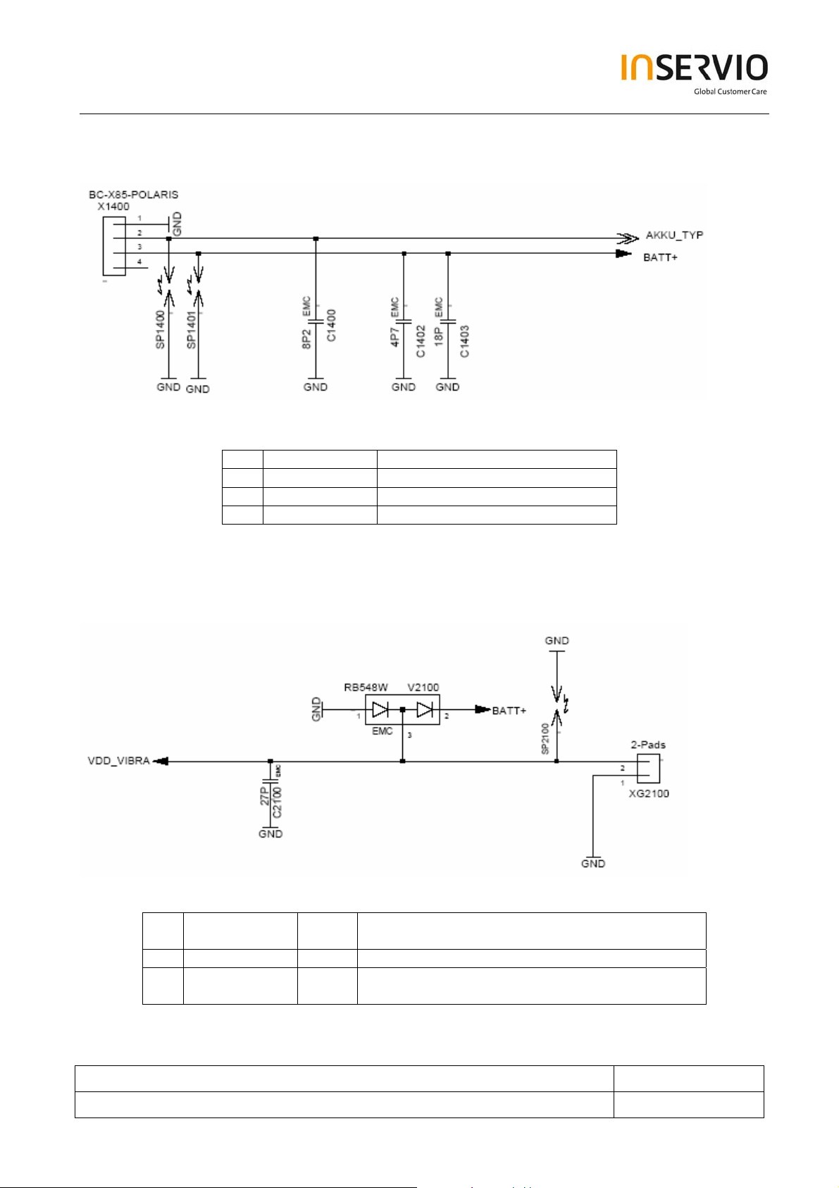
13.2 Battery (X1400)
Pin Name Remarks
1 GND Ground
2 AKKU_TYP Recognition of battery/supplier
3 BATT+ Positive battery pole
13.3 Vibration Motor (XG2100)
Pin Name IN/OUT Remarks
1 GND
2 VDD_VIBRA Vbatt will be switched by PWM-signal with
internal FET to VDD_Vibra in Asic
Technical Documentation Release 1.0
TD_Repair_L3 _Theory of Operation_E71_R1.0.pdf Page 29 of 35
Created by inservio GmbH for BenQ mobile GmbH & Co. OHG - Company Confidential2006©inservio
Page 30
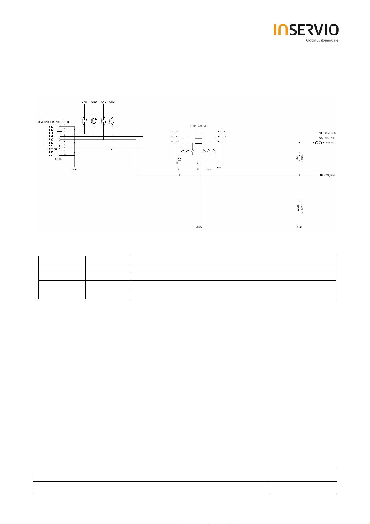
13.4 Interface SIM Module with ESD protection
Pin Name IN/OUT Remarks
SIM_CLK O Pulse for chipcard. The SIM is controlled directly from the SGOLD.
SIM_RST O Reset for chipcard
SIM_IO I/O Data pin for chipcard
VDD_SIM O Switchable power supply for chipcard;
The Z1601 is a 3-channel filter with over-voltage and ESD Protection array which is designed to
provide filtering of undesired RF signals. Additionally diodes are contained to protect downstream
components from Electrostatic Discharge (ESD) voltages
Technical Documentation Release 1.0
TD_Repair_L3 _Theory of Operation_E71_R1.0.pdf Page 30 of 35
Created by inservio GmbH for BenQ mobile GmbH & Co. OHG - Company Confidential2006©inservio
Page 31
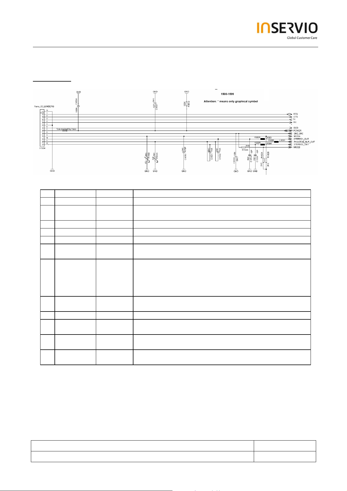
13.5 Nano IO Connector with ESD protection
IO Connector
Pin Name IN/OUT Notes
1 D+/RTS I/O Use as RTS in data-operation.
2 D+/CTS I/O Data-line for accessory-bus
Use as CTS in data operation.
3 TX O Serial interface
4 RX I Serial interface
5 GND
6 FLASH/DCD I/O Clock-line for accessory-bus.
Use as DTC in data-operation.
7 POWER I/O POWER is needed for charging batteries and for supplying
the accessories. If accessories are supplied by mobile, talk-
time and standby-time from telephone are reduced.
Therefore it has to be respected on an as low as possible
power consumption in the accessories.
8 GND_MIC Analog I for ext. microphone driving ext. left speaker
9 MICP2 Analog I External microphone
10 AUDIO_R Analog O driving ext. right speaker
With mono-headset Audio_L and Audio_R differential Signal
11 AUDIO_REF Analog O mid-voltage in stereo mode refernce to AUDIO_L and
AUDIO_R in mono mode not used
12 AUDIO_L Analog O driving ext. left speaker
With mono-headset Audio_L and Audio_R differential mode
Technical Documentation Release 1.0
TD_Repair_L3 _Theory of Operation_E71_R1.0.pdf Page 31 of 35
Created by inservio GmbH for BenQ mobile GmbH & Co. OHG - Company Confidential2006©inservio
Page 32

ESD Protection with EMI filter
The Z1501 is a 5-channel filter with over-voltage and ESD Protection array which is designed to
provide filtering of undesired RF signals in the 800-4000MHz frequency band Additionally the Z1501
contains diodes to protect downstream components from Electrostatic Discharge (ESD) voltages
Technical Documentation Release 1.0
TD_Repair_L3 _Theory of Operation_E71_R1.0.pdf Page 32 of 35
Created by inservio GmbH for BenQ mobile GmbH & Co. OHG - Company Confidential2006©inservio
Page 33

13.6 Display Connector
Pin Number Pin Name Description
1 DISP_RESET1 Display Reset
2 DISP_D1 Data Line
3 DISP_D0 Data Line
4 GND Ground
5 DISP_CD Data command select signal
6 2,9V Power Supply
7 2,65V Power Supply for LED
8 DISP_CS1 Chipset signal
9 LCD_BCKLT Signal for Backlight Illumination
10 VBOOST Power Supply for LED
11 DISP_VD Synch Pin
12 GND Ground
13 DISP_WR Write signal
14 DISP_RD Read signal
15 DISP_D2 Data Line
16 DISP_D3 Data Line
17 DISP_D4 Data Line
18 DISP_D5 Data Line
19 DISP_D6 Data Line
20 DISP_D7 Data Line
21 GND Ground
22 GND Ground
23 GND Ground
24 GND Ground
Technical Documentation Release 1.0
TD_Repair_L3 _Theory of Operation_E71_R1.0.pdf Page 33 of 35
Created by inservio GmbH for BenQ mobile GmbH & Co. OHG - Company Confidential2006©inservio
Page 34

13.7 MMI Connector
Pin Number Pin Name Description
1 VBOOST Power Supply for LED
2 GND Ground
3 KP_OUT2 Keypad Matrix Line
4 KP_OUT1 Keypad Matrix Line
5 KP_OUT0 Keypad Matrix Line
6 KP_IN0 Keypad Matrix Line
7 KP_IN1 Keypad Matrix Line
8 KP_IN2 Keypad Matrix Line
9 KP_IN3 Keypad Matrix Line
10 KP_IN4 Keypad Matrix Line
11 KP_ON_OFF ON OFF Key
12 KPD_BCKLT Signal for Keypad Illumination
13 KP_OUT3 Keypad Matrix Line
14 KPI_IN5_OUT6 Keypad Matrix Line
Technical Documentation Release 1.0
TD_Repair_L3 _Theory of Operation_E71_R1.0.pdf Page 34 of 35
Created by inservio GmbH for BenQ mobile GmbH & Co. OHG - Company Confidential2006©inservio
Page 35

g
g
d
13.8 Camera Connector
Pin Number Pin Name Description
1 GND Ground
2 CAM_CLKOUT Camera Clock Signal
3 GDN Ground
4 CAM_PCLK Pixel Clock Signal
5 GND Ground
6 I2C_2_DAT I2C Bus Data Line
7 I2C_2_CLKT I2C Bus Clock Line
8 GND Ground
9 CAM_HSYNC Horizontal Synch Line
10 CAM_VSYNC Vertical Synch Line
11 GND Ground
12 CAM_DAT7 Data Line
13 CAM_DAT6 Data Line
14 CAM_DAT5 Data Line
15 CAM_DAT4 Data Line
16 CAM_DAT3 Data Line
17 CAM_DAT2 Data Line
18 CAM_DAT1 Data Line
19 CAM_DAT0 Data Line
20 DVDD Camera Voltage Supply from N3500
14 E71 Diagram Sets
Double click the tag symbol to open the files.
TD_Repair_E71
Dia
ram S et_R1.0.pd
^
Technical Documentation Release 1.0
TD_Repair_L3 _Theory of Operation_E71_R1.0.pdf Page 35 of 35
Created by inservio GmbH for BenQ mobile GmbH & Co. OHG - Company Confidential2006©inservio
TD_Repair_E71_Logi
c Di agram_R1 .0.pdf
TD_Repair_E71_R F _
HIT_Dia
ram_R1.0.p
 Loading...