

Page 1
Release 1.0
Service Repair Documentation
Level 3 - E61
Release Date Department Notes to change
R 1.0
Technical Documentation
TTD_Repair_L3 _Theory of Operation_E61_R1.0.pdf Page 1 of 33
12.05.2006 BenQ S CC CES New document
06/2006
Page 2

Release 1.0
Table of Content
1 Introduction ...............................................................................................................................3
1.1 PURPOSE...............................................................................................................................3
1.2 SCOPE ...................................................................................................................................3
1.3 TERMS AND ABBREVIATIONS ...................................................................................................3
2 List of available level 3 parts....................................................................................................4
3 Required Equipment for Level 3 ..............................................................................................6
4 Required Software for Level 3..................................................................................................6
5 Radio Part ..................................................................................................................................7
5.1 RECEIVER OPERATION............................................................................................................7
5.2 TRANSMITTER OPERATION......................................................................................................8
5.3 VCXO OPERATION.................................................................................................................9
6 Logic (Base-Band)...................................................................................................................10
6.1 CALYPSO..............................................................................................................................12
6.2 IOTA....................................................................................................................................15
6.3 POWER SUPPLY ...................................................................................................................19
6.3.1 System power on/off Sequence ...................................................................................20
6.4 MEMORY CIRCUIT .................................................................................................................21
6.5 LCD MODULE (LCDM)..........................................................................................................23
6.6 CAMERA MODULE.................................................................................................................24
7 Interfaces .................................................................................................................................25
7.1 AUDIO CODEC AND AUDIO AMPLIFIER....................................................................................25
7.1.1 Audio codec function block...........................................................................................25
7.1.2 Multimedia Application Input Circuit Design.................................................................26
7.1.3 Multimedia Application Output Circuit Design..............................................................27
7.1.4 Loudspeaker output path and D-amplifier design.........................................................27
7.2 10 PINS I/O CONNECTOR ......................................................................................................28
7.3 MINI-SD CARD .....................................................................................................................29
7.4 KEYPAD LED CIRCUIT...........................................................................................................30
7.5 VIBRATOR ............................................................................................................................30
7.6 KEYPAD................................................................................................................................31
8 Charging circuit.......................................................................................................................33
Technical Documentation
TTD_Repair_L3 _Theory of Operation_E61_R1.0.pdf Page 2 of 33
06/2006
Page 3

Release 1.0
1 Introduction
1.1 Purpose
This Service Repair Documentation is intended to carry out repairs on BenQ repair level 3-4.
1.2 Scope
This document is the reference document for all BenQ authorised Service Partners which are
released to repair Siemens mobile phones up to level 3.
1.3 Terms and Abbreviations
Technical Documentation
TTD_Repair_L3 _Theory of Operation_E61_R1.0.pdf Page 3 of 33
06/2006
Page 4
Release 1.0
2 List of available level 3 parts
Product ID Order Number Description CM
E61
E61
E61
E61
E61
E61
E61
E61
E61
E61
E61
E61
E61
E61
E61
E61 RT1 L50622-f4103-k NTC10K0402NTH5GBQ6J.60009.001
E61 T9 L50640-D110-D670 DISDIODETVM0A090MIRYBQ6J.80009.011
E61 T2 L50640-D128-D670 DISDIODESFI0402ML120CBQ6J.80018.011
E61 T3 L50640-D128-D670 DISDIODESFI0402ML120CBQ6J.80018.011
E61 T4 L50640-D128-D670 DISDIODESFI0402ML120CBQ6J.80018.011
E61 T1 L50640-D129-D670 DISDIODE0402-050E560NPBQ6J.80018.031
E61 T5 L50640-D129-D670 DISDIODE0402-050E560NPBQ6J.80018.031
E61 T7 L50640-D129-D670 DISDIODE0402-050E560NPBQ6J.80018.031
E61 T8 L50640-D129-D670 DISDIODE0402-050E560NPBQ6J.80018.031
E61 CB57 L50640-D130-D670 DISDIODESFI0402-050E47BQ6J.80018.041
E61 CB58 L50640-D130-D670 DISDIODESFI0402-050E47BQ6J.80018.041
E61 TVS4C1 L50640-D119-D670 DISDIODETVSSFI0508-050RBQ6J.80022.011
E61 TVS4C2 L50640-D119-D670 DISDIODETVSSFI0508-050RBQ6J.80022.011
E61 CN1 L50664-F6220-K CAPARRAY22P50VJ0805SBQ7G.62203.0C1
E61 CN2 L50664-F6220-K CAPARRAY22P50VJ0805SBQ7G.62203.0C1
E61 CN3 L50664-F6220-K CAPARRAY22P50VJ0805SBQ7G.62203.0C1
E61 DN1 L50640-D5121-D670 DISDIODEARRDAN222BQ8C.00222.0A0
E61 D601 L50640-D124-D670 DISDIODEVARHVD358BKRF-EBQ8C.00358.090
E61 D1 L50640-D5110-D670 DISDIODERB520S-30BQ8C.00520.080
E61 LED3 L50640-L2179-D670 DISOPT19-213AUWD/S365-2BQ8C.19213.071
E61 LED4 L50640-L2179-D670 DISOPT19-213AUWD/S365-2BQ8C.19213.071
E61 LED5 L50640-L2179-D670 DISOPT19-213AUWD/S365-2BQ8C.19213.071
E61 LED6 L50640-L2179-D670 DISOPT19-213AUWD/S365-2BQ8C.19213.071
DCJ
SPCON
LCDM
DSC
BATC1
BATC2
IOJ
ANT1
KPCON
SIM
MINISD
TKCON1
TKCON2
F1
F2
L50634-Z97-C553 CONNDCPWRPA05302-QNJBQ2B.13120.021
L50634-Z97-C557 CONN24PD.4H1.5AXK824145YBQ2K.L1142.024
L50634-Z97-C562 CONN30PD5H185AXK5F30545YBQ2K.L1143.030
L50634-Z97-C668 CONNSKT24PD.4AXK724245BQ2K.L1165.024
L50634-Z97-C664 CONNBATTCBE-3111-2769HBQ2K.N0079.011
L50634-Z97-C665 CONNBATT2PJ-3111H-2-25BQ2K.N0079.071
L50634-Z97-C558 CONNI/O10PP0.5BQ2K.N0081.001
L50634-Z97-C666 CONNSPRING2PN027M4-2I3BQ2K.N0082.031
L50634-Z97-C667 CONNBTB14PFBF05314BQNBQ2K.N1003.021
L50634-Z97-C659 CONNSIMCARDBM05106-L5BQ2K.N5030.021
L50634-Z97-C669 CONNSDMINI11P48050-3BQ2K.N5037.011
L50634-Z97-C670 CONNVOLUMAV4040-A0G12BQ2K.P0003.004
L50634-Z97-C670 CONNVOLUMAV4040-A0G12BQ2K.P0003.004
L50645-A820-Y48 FUSE1.25A32VF04671BQ6J.41251.001
L50645-A820-Y48 FUSE1.25A32VF04671BQ6J.41251.001
Technical Documentation
06/2006
TTD_Repair_L3 _Theory of Operation_E61_R1.0.pdf Page 4 of 33
Page 5

Release 1.0
E61 LED7 L50640-L2179-D670 DISOPT19-213AUWD/S365-2BQ8C.19213.071
E61 LED8 L50640-L2179-D670 DISOPT19-213AUWD/S365-2BQ8C.19213.071
E61 LED9 L50640-L2179-D670 DISOPT19-213AUWD/S365-2BQ8C.19213.071
E61 LED10 L50640-L2179-D670 DISOPT19-213AUWD/S365-2BQ8C.19213.071
E61 D4 L50640-D5123-D670 DISDIODERB161M-20BQ8C.1R002.08Q
E61 D5 L50640-D5124-D670 DISDIODEPMEG2020EJBQ8C.2R002.A8F
E61 D601 L50640-D5124-D670 DISDIODEPMEG2020EJBQ8C.2R002.A8F
E61 DZB1 L50640-D3142-D670 DISDIODEZEN6.06-6.33VBQ8C.6R205.03F
E61 D2 L50640-D5125-D670 DISDIODE1PS79SB30BQ8C.R2004.A84
E61 D3 L50640-D5125-D670 DISDIODE1PS79SB30BQ8C.R2004.A84
E61 B1 L50640-C2149-D670 DISTRANSPEMH9NPNBQ8D.00009.010
E61 B3 L50640-C2167-D670 DISTRANSUMH10NNPNBQ8D.00010.01F
E61 B2 L50640-C2143-D670 DISTRANSBC807-40WPNPBQ8D.00807.A1K
E61 FN1 L50630-C1198-D670 DISTRANSFDG6303NBQ8D.06303.03K
E61 FP1 L50630-C1186-D670 DISTRANSFETFDC6306PBQ8D.06306.030
E61 FP3 L50630-C1186-D670 DISTRANSFETFDC6306PBQ8D.06306.030
E61 FP2 L50630-C1187-D670 DISTRANSFETFDC6506PBQ8D.06506.030
E61 U67 L50645-K280-Y420 FILSAW1842.5MHZSAFEH1GBQ6J.10151.001
E61 U68 L50645-K280-Y421 FILSAW942.5MHZSAFEH942MBQ6J.10152.001
E61 U66 L50645-K280-Y437 FILSAW1960MHSAFEH1G96FBBQ6J.10154.001
E61 EMI2 L50645-K280-Y453 FILLFA24-2A1A144MTBQ6J.10189.001
E61 EMI3 L50645-K280-Y453 FILLFA24-2A1A144MTBQ6J.10189.001
E61 EMI4 L50645-K280-Y453 FILLFA24-2A1A144MTBQ6J.10189.001
E61 EMI5 L50645-K280-Y453 FILLFA24-2A1A144MTBQ6J.10189.001
E61 EMI6 L50645-K280-Y467 FILLFB20-3D1E471MBQ6J.10189.011
E61 EMI7 L50645-K280-Y467 FILLFB20-3D1E471MBQ6J.10189.011
E61 IOTA L50610-U6243-D670 ICINTFTWL3025BZGMRBQ7A.03025.B0U
E61 SHJ2SL L50610-G6322-D670 ICCPUSH7327-DH6417327BQ7A.07327.00U
E61 G2 L50645-J4683-Y34 ICASICD751992AZHHRBQ7A.75199.A0U
E61 AND1 L50610-B6250-D670 ICLOGINL17SZ08XV5T2BQ7C.17085.090
E61 AND2 L50610-B6250-D670 ICLOGINL17SZ08XV5T2BQ7C.17085.090
E61 OR1 L50610-B6251-D670 ICLOGINL17SZ32XV5T2BQ7C.17325.09H
E61 BR13M L50610-B6252-D670 ICLOGISN74AVC1T45DCKRBQ7C.74145.09H
E61 BR32K L50610-B6252-D670 ICLOGISN74AVC1T45DCKRBQ7C.74145.09H
E61 BRRSTO L50610-B6252-D670 ICLOGISN74AVC1T45DCKRBQ7C.74145.09H
E61 AMP L50610-C6390-D670 ICANATPA2010D1YZFRBQ7D.02010.0K0
E61 U1 L50610-C6392-D670 ICANANUF2221W1T2GBQ7D.02221.07Y
E61 BLDRV L50610-C6288-D670 ICDCCONLM3501TLXBQ7D.03501.040
E61 LDO2CH L50610-C6423-D670 ICVRR5325K005B-TRBQ7D.05325.030
E61 U64 L50610-U6248-D670 ICSWITCHPLELMSP54CA-272BQ7D.054CA.D30
E61 PMIC L50610-C6394-D670 ICANABH6053GUBQ7D.06053.04U
E61 CHRIC L50610-C6395-D670 ICANAISL6292CCR3ZBQ7D.06292.070
E61 CODEC L50610-U6276-D670 ICAUDIOWM8955LSEFL/RBQ7D.08955.075
Technical Documentation
06/2006
TTD_Repair_L3 _Theory of Operation_E61_R1.0.pdf Page 5 of 33
Page 6
Release 1.0
E61 U70 L50610-C6289-D670 ICANAVRMAS9124A2GC06BQ7D.09124.03B
E61 VD1 L50610-C6424-D670 ICDETECTORXC61GN2302HRNBQ7D.12302.0B0
E61 U65 L50610-U6244-D670 ICIRXCVRHD155165BPEBBQ7D.15516.0FU
E61 U69 L50610-C6425-D670 ICPWRAMPSKY77328BQ7D.77328.0K0
E61 U62 L50610-B6218-D670 ICLOGIBUFFERNC7WZ16BQ7D.7WZ16.0MY
E61 O48M L50645-G200-Y28 OSC48MHZ30PF50PPMBQ8B.24800.301
E61 U61 L50645-F102-Y48 OSCCRYST26MHZU-860-1-1BQ8B.30026.D02
E61 C30M L50645-F102-Y64 OSCCRYST30MHZ30MHZ8PFBQ8B.33000.B02
E61 C32K L50645-F102-Y49 OSCCRYST32.768DST520BQ8B.33276.705
3 Required Equipment for Level 3
GSM-Tester
PC-incl. Monitor, Keyboard and Mouse
USB boot cable with USB foxlink driver (F30032-P601-A1)
Troubleshooting Frame E61
Power Supply
Spectrum Analyser
Active RF-Probe incl. Power Supply
Oscilloscope incl. Probe
RF-Connector (N<>SMA(f))
Power Supply Cables
Dongle
BGA Soldering equipment
4 Required Software for Level 3
Windows XP
XCSD Tools Level 3
GRT Version 4 or higher
Technical Documentation
TTD_Repair_L3 _Theory of Operation_E61_R1.0.pdf Page 6 of 33
06/2006
Page 7
Release 1.0
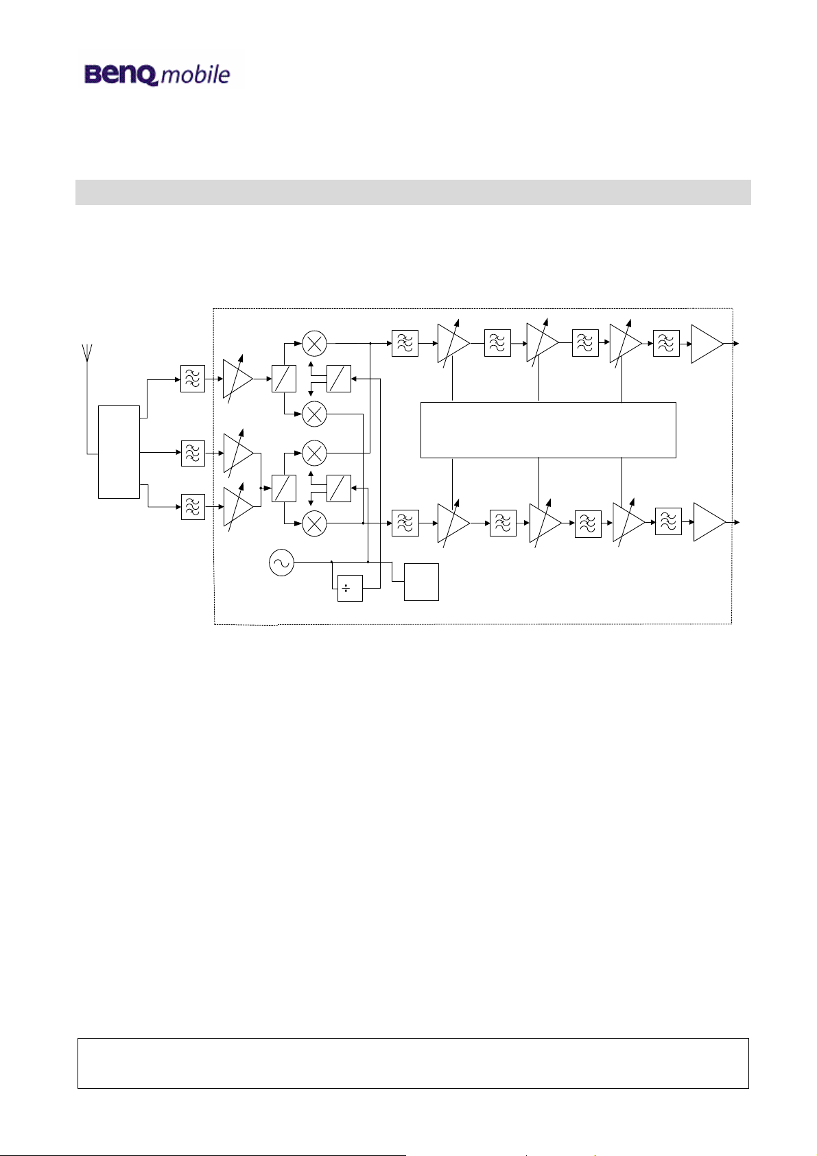
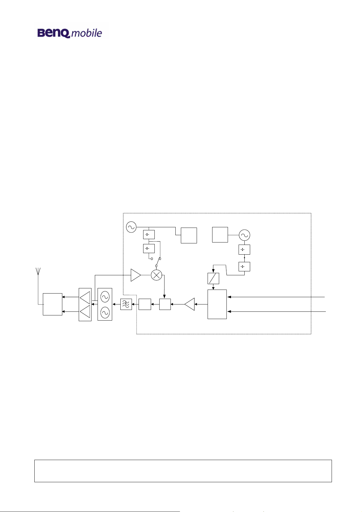
5 Radio Part
5.1 Receiver Operation
IRxP
IRxN
QRxP
QRxN
RX GSM: 925~960 MHz
T/R
Switch
1805~1880 MHz
1930~1990 MHz
DCS:
PCS:
GSM LNA
0
90
DCS LNA
0
90
PCS LNA
RFVCO
PCS:3860~3980 MHz
DCS:3610~3760 MHz
GSM:3700~3840 MHz
0
90
Shift(1/2)
0
90
Shift(1/2)
2
GSM:
1850~1920 MHz
DCS:
1805~1880 MHz
PCS:
1930~1990 MHz
RF
Synth
ADC/DAC & Control Logic for DC Offset Cancellation
HD155165BP (B6E)
The Receiver structure in HD155165BP is a zero-IF solution. That means RF signal is directly downconverted to the baseband signal. And by the way, all of the DC-offset canceling processes
are done within chip. We do not have to care about that.
The LNA amplifies the RF signal after passing the T/R switch and RF SAW filter and before it enters
the down-converter section. The RF signal is mixed with a local oscillator (LO) signal to generate the
baseband signal.
Three LPFs are used in the baseband signal processing for reducing blocking signals. The first LPF
employs two external capacitors, and we can check whether the front-end (LNA + Mixer) is
functionally well or not by probing these two capacitors to see if there is any baseband
signal(<200kHz).
After three stages of DC-offset cancelling, the signal (I+/I-/Q+/Q-) then output to the baseband IC for
further processing.
The HD155165BP receiver is based upon the HD155155NP direct conversion design. As
HD155165BP supports quad band, the front end incorporates four LNAs and mixers. The incoming
RF signals are mixed directly down to I/Q base-band by the front-end block. This incorporates four
LNAs / four buffers and Gilbert Cell mixer blocks optimized for operation at 850MHz, 900MHz,
1800MHz, and 1900MHz respectively.
The front-end block is followed by two closely matched base-band amplifier chains. These include
distributed low pass filter, three switched gain stages and one fixed gain stage.
Technical Documentation
06/2006
TTD_Repair_L3 _Theory of Operation_E61_R1.0.pdf Page 7 of 33
Page 8
Release 1.0
In addition, the base-band section integrates A/D and D/A converters which provide automatic onchip correction of DC offsets. The three switched gain stages in each channel are DC coupled and
provide 90dB gain control range with 2dB step size. The first PGA has a voltage gain range (x8-x1)
with 6dB steps. The second PGA has a gain range (x8-x0.125) with 2dB steps. The third PGA has a
gain range (x8-x0.125) with 2dB steps. The final fixed gain amplifier provides a gain of x3 or x6. The
gain is set to match the on-chip levels to the input dynamic range of the base-band. The base-band
filtering in each channel comprises a single RC low pass filter at the input of the first switched gain
stage and three 2nd order Butterworth filters, one at the input of each of the other switched gain
stages. The R/C filter requires an off-chip capacitor for each channel. The Butterworth filters are fully
integrated on-chip.
The base-band PGA includes a DC offset cancellation system. The auto calibration system uses a
successive approximation technique and requires around 20us to perform a three stages calibration.
The system calibrates out the offsets arising in both I and Q receives channels.
5.2 Transmitter Operation
PCS:3860~3980 MHz
DCS:3580~3730 MHz
RFVCO
GSM:3840~3980 MHz
2
2
GSM
GSM: 960~995 MHz
RF
DCS/
PCS
PCS:1930~1990 MHz
DCS:1790~1865 MHz
Synth
IF
Synth
IFVCO
640/656 MHz
2
2
0
T/R
Switch
Quad-Band PA
TX GSM: 880~ 915 MHz
DCS:1710~1785 MHz
PCS:1850~1910 MHz
Loop Filter
Charge
Pump
Shift(1/2)
PFD
80/82 MHz
90
I&Q Mod
ITxP
ITxN
QTxP
QTxN
HD155165BP (B6E)
The B6E generates a modulated signal at IF with a quadrature modulator and converts it to final
frequency with an Offset Phase Locked Loop (OPLL).
The Offset Phase Locked Loop is simply a PLL with a down conversion mixer in the feedback path.
Using a down converter in the feedback path acts as an up-converter in the forward path. This
allows the output frequency to be different from the comparison frequency without affecting the
normal operation of the loop. Phase/frequency changes in the reference signal are not scaled, as
they would be if a divider were used in the feedback path, hence the modulation is faithfully
reproduced at the final frequency.
The main advantage of the OPLL in this application is that it forms a tracking band pass filter around
the modulated signal. This is because the loop cannot respond to phase variations at the reference
that are outside its closed loop bandwidth. Thus the broad band phase noise from the quadrature
modulator is shaped by the frequency response of the closed loop allowing the TX noise
specification to be met without further filtering.
Technical Documentation
06/2006
TTD_Repair_L3 _Theory of Operation_E61_R1.0.pdf Page 8 of 33
Page 9
Release 1.0
A secondary advantage of the OPLL is that the output signal, coming from a VCO, is truly constant
envelope. This removes the problem of spectral spreading caused by AM to AM and AM to PM
conversion in the power amplifier.
The OPLL is formed from an on chip Gilbert cell down converter, limiter and phase detector with on
chip passive loop filter. The phase detector is implemented as a Gilvert cell with current source
output stage. The current output allows an integrator to be included in the passive loop filter. This is
similar to the technique commonly used in PLL synthesizers. A digital phase detector is used to
speed OPLL locking. After locking, the digital phase detector is switched off and the analogue phase
detector becomes active.
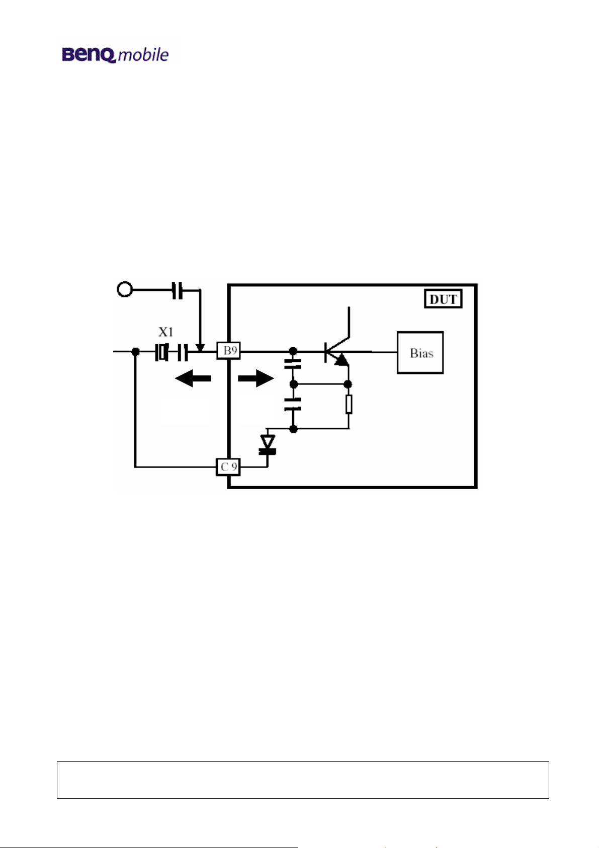
5.3 VCXO Operation
+R
HD155165BP provides a DCXO function. With that function, we can build a reference clock
generation circuits as shown in the above graph. This means that the VCTCXO module is not
necessary for clock application, and only one crystal with 8ppm tolerance and one varactor are
enough.
The transistor in HD155165BP and two internal capacitors (C1, C2) provide a negative resistance,
and the crystal (X1) combined with some other passive components to provide a positive resistance.
When these two resistance values equal to each other at some frequency, the oscillation will happen
at that frequency. In our design target, the oscillation frequency should be within 26MHz +/-15 ppm
at least.
-R
Technical Documentation
TTD_Repair_L3 _Theory of Operation_E61_R1.0.pdf Page 9 of 33
06/2006
Page 10
Release 1.0
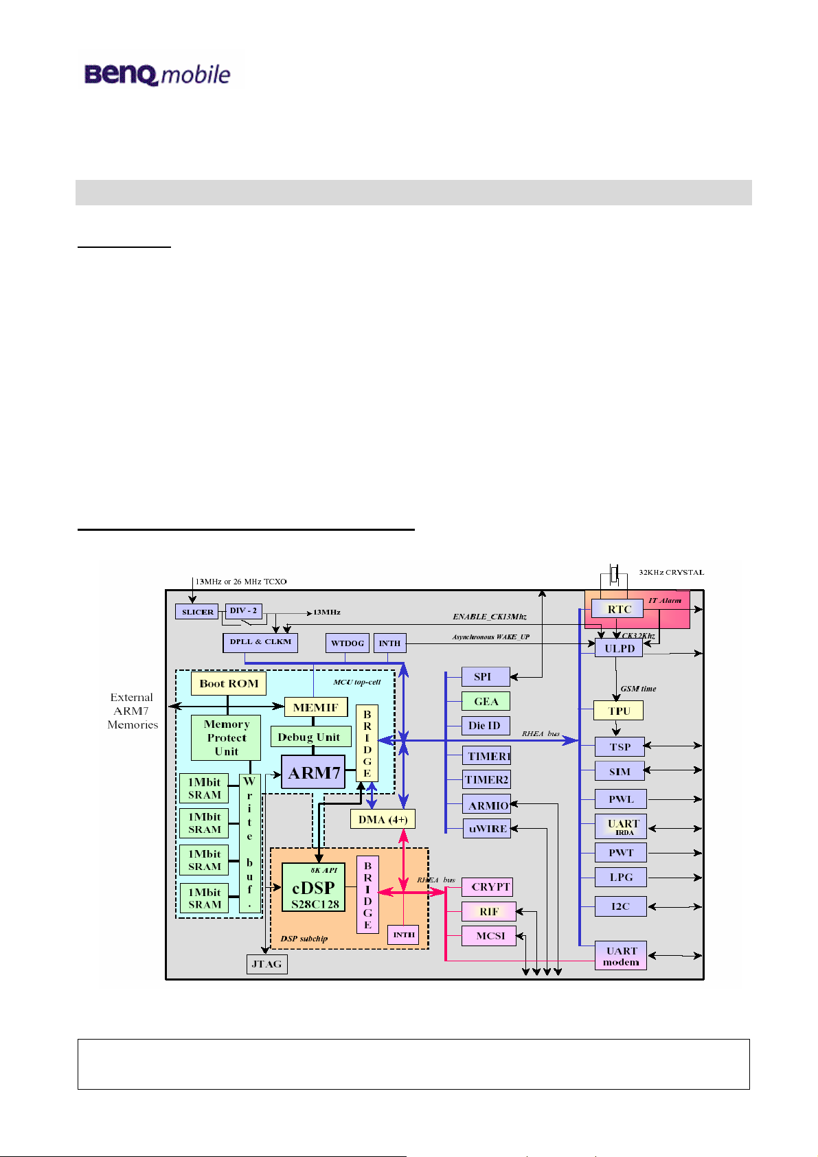
6 Logic (Base-Band)
Introduction:
E61 utilizes TI’s chipsets (CALYPSO and IOTA) and RENESAS’s chipset (SHJ2SLSL) as baseband solution. Base-band is composed with three potions: Logic, Analog/Codec and MMP.
CALYPSO is a GSM/GPRS digital base-band logic solution included microprocessor, DSP, and
peripherals. IOTA is a combination of analog/codec solution and power management which contain
base-band codec, voice-band codec, several voltage regulators and SIM level shifter etc.
SHJ2SLSL is a multimedia solution included microprocessor, DSP, internal memory, and interrupt
controller. In addition, HerB1A integrates with other features such as LED backlight, TFT-LCD
display, CMOS DSC module, Mini-SD card, vibration, SW-midi, MP3 and charging etc. The following
sections will present the operation theory with circuitry and descriptions respectively.
Block Diagram CPU CALYPSO (HERCROM400)
Technical Documentation
TTD_Repair_L3 _Theory of Operation_E61_R1.0.pdf Page 10 of 33
06/2006
Page 11

IOTA
Release 1.0
Technical Documentation
TTD_Repair_L3 _Theory of Operation_E61_R1.0.pdf Page 11 of 33
06/2006
Page 12

Release 1.0
6.1 Calypso
CALYPSO (HERCROM400) is a chip implementing the digital base-band processor of a
GSM/GPRS mobile phone. This chip combines a DSP sub-chip (LEAD2 CPU) with its program
and data memories, a Micro-Controller core with emulation facilities (ARM7TDMIE) and an
internal 4M-bit RAM memory, a clock squarer cell, several compiled single-port or 2-ports RAM
and CMOS gates.
Major functions of this chip are as follows:
Real Time Clock (RTC)
The RTC block is an embedded RTC module fed with an external 32.768 KHz Crystal. Its basic
functions are:
1. Time information (seconds/minutes/hours)
2. Calendar information (Day/Month/Year/ Day of the week) up to year 2099
3. Alarm function with interrupts (RTCINT is generated to wake up ABB)
4. 32 KHz oscillator frequency gauging
Pulse Width Light (PWL)
This module allows the control of the backlight of LCD and keypad by employing a 4096 bit
random sequence .In the 56E30, we use the LT/PWL function to turn on the keypad light LED.
MODEM-UART
This UART interface is compatible with the NS 16C750 device which is devoted to the
connection to a MODEM through a standard wired interface. The module integrates two 64
words (9 and 11 bits) receive and transmit FIFOs which trigger levels are programmable. All
modem operations are controllable either via a software interface or using hardware flow control
signals. In E61, we implement software flow control by only two signals: TXD0 and RXD0.
General Purposes I/O (GPIO)
Calypso provides 16 GPIOs configurable in read or write mode by internal registers. In E61, we
utilize all of them as follows:
IO0: Let MMP power-on reset; ‘Low active’
IO1: Enable LCDM backlight;
:
IO2: Control MMP’s MFI mode; ‘H’
IO3: Switching SWREG output voltage; ’H’
IO4: MMP’s MFI INT request; ‘Low active’
Technical Documentation
68-type mode, ‘L’:80-type mode
:
SWREG mode, ’L’:REG_L mode
06/2006
TTD_Repair_L3 _Theory of Operation_E61_R1.0.pdf Page 12 of 33
Page 13

Release 1.0
IO5: SIM power control
IO6: Reserve
IO7: Reset of external device: For HerB1A, TFT LCDM
IO8: Indicates whether MMP is in software standby mode
IO9: Enable audio amplifier;
IO10: Detection of mini-SD card
IO11: Reserve
IO12: Reserve
IO13: INT request for MMP
IO14: SRAM high-byte enable
IO15: SRAM low-byte enable
Serial Port Interface (SPI)
The SPI is a full-duplex serial port configurable from 1 to 32 bits and provides 3 enable signals
programmable either as positive or negative edge or level sensitive. This interface is working on
13MHz and is used for the GSM/GPRS baseband and voice A/D, D/A with IOTA
Memory Interface and internal Static RAM
For external memory device (Flash and SRAM), this interface performs read and write access
with adaptation to the memory width. It also provides 6 chip-select signals corresponding each
to an address range of 8 mega bytes. One of these chip-select is dedicated to the selection of
an internal memory. In E61, we employ nCS0/nCS1 (nCS0_NROM/nCS1_NROM) for external
Flash and nCS2 (nCS2_NSRAM) for external SRAM.
A 4Mbit SRAM is embedded on the die and memory mapped on the chip-select nCS6 of the
memory interface.
SIM Interface
The Subscriber Identity Module interface will be fully compliant with the GSM 11.11 and ISO/IEC
7816-3 standards. Its external interface is 3 Volts only. 5 Volts adaptation will be based on
external level shifters.
JTAG
In E61, JTAG is used for software debugging.
Technical Documentation
TTD_Repair_L3 _Theory of Operation_E61_R1.0.pdf Page 13 of 33
06/2006
Page 14

Release 1.0
Time Serial Port (TSP)
The TPU is a real-time sequencer dedicated to the monitoring of GSM/GPRS baseband
processing. The TSP is a peripheral of the TPU which includes both a serial port (32 bits) and a
parallel interface. The serial port can be programmed by the TPU with a time accuracy of the
quarter of GSM bit. The serial port is uni-directional (transmit only) when used with IOTA. The
serial port provides 4 enable signals programmable either as positive or negative edge or level
sensitive. This serial port is derived from 6.5MHz and used to control the real time GSM windows
for the baseband codec and the windows for ADC conversion.
TSP Parallel interface (ACT)
The parallel interface allows control 13 external individual outputs and 1 internal signal with a
time accuracy of the quarter of GSM bit. These parallel signals are mainly used to control the RF
activity. In E61, we employ 7 of them to control RF activity.
TSPACT1: GSM_T/R
TSPACT2: DCS_T/R
TSPACT3: PCS_RX
TSPACT6: TX_ON
TSPACT8: Crystal enable
TSPACT9: Band select
TSPACT10: Three wires latch enable
Radio Interface (RIF)
The RIF (Radio Interface) Module is a buffered serial port derived from the BSP peripheral
module of the defined for TMS320C5X. The external serial data transmission is supported by a
full-duplex double-buffered serial port interface. The interface is used for transfer of baseband
transmit and receive data and also to access all internal programmation registers of the device.
Miscellaneous:
Some important Baseband /RF interface signals are defined as follows:
CLKTCXO: 13MHz VTCXO Clock from RF circuit
TCXOEN: 13MHz VTCXO Clock Enable signal
Technical Documentation
TTD_Repair_L3 _Theory of Operation_E61_R1.0.pdf Page 14 of 33
06/2006
Page 15

Release 1.0
6.2 IOTA
Together with a digital base-band device (Calypso), IOTA is part of a TI DSP solution intended for
digital cellular telephone applications including GSM 900, DCS 1800 and PCS 1900 standards
(dual band capability).
It includes a complete set of base-band functions to perform the interface and processing of voice
signals, base-band in-phase (I) and quadrature (Q) signals which support single-slot and multislot mode, associated auxiliary RF control features, supply voltage regulation, battery charging
control and switch ON/OFF system analysis. IOTA interfaces with the digital base-band device
through a set of digital interfaces dedicated to the main functions of Calypso-Lite, a base-band
serial port (BSP) and a voice-band serial port (VSP) to communicate with the DSP core (LEAD),
a micro-controller serial port to communicate with the micro-controller core and a time serial port
(TSP) to communicate with the time processing unit (TPU) for real time control.
IOTA also includes on chip voltage reference, under voltage detection and power-on reset
circuits.
Major functions of this chip are as follows:
Baseband Codec (BBC)
The baseband codec includes a two-channel uplink path and a two-channel downlink path.
The baseband uplink path (BUL) modulates the bursts of data coming from the DSP via the
baseband serial port (BSP) and to be transmitted at the antenna. Modulation is performed by a
GMSK modulator. The GMSK modulator implemented in digital technique generates In-phase (I)
and Quadrature (Q) components, which are converted into analog base-band by two 10 bits
DACs filters. It also includes secondary functions such as DC offset calibration and I/Q gain
unbalance.
The baseband downlink path (BDL) converts the baseband analog I & Q components coming
from the RF receiver into digital samples and filters these resulting signals through a digital FIR
to isolate the desired data from the adjacent channels. During reception of burst I & Q digital
data are sent to the DSP via the baseband serial port (BSP) at a rate of 270 KHz.
Automatic Frequency control (AFC)
The automatic frequency control function consists of a digital to analog converter optimized for
high resolution DC conversion. Its purpose is to control the frequency of the GSM 13MHz
oscillator to maintain mobile synchronization on the base station and allow proper transmission
and demodulation.
Technical Documentation
TTD_Repair_L3 _Theory of Operation_E61_R1.0.pdf Page 15 of 33
06/2006
Page 16

Release 1.0
Automatic Power Control (APC)
Purpose of the Automatic Power Control (APC) is to generate an envelope signal to control the
power ramping up, ramping down and power level of the radio burst.
The APC structure is intended to support single slot and multi-slots transmission with smooth
power transition when consecutive bursts are transmitted at different power level. It includes a
DAC and a RAM in which the shape of the edges (ramp-up and ramp-down) of the envelope
signals are stored digitally. This envelope signal is converted to analog by 10 bits digital to analog
converter. Timing of the APC is generated internally and depends of the real time signals coming
from the TSP and the content of two registers which control the relative position of the envelope
signal versus the modulated I & Q.
Time serial port (TSP)
Purpose of the time serial port is to control in real time the radio activation windows of IOTA
which are BUL power-on, BUL calibration, BUL transmit, BDL power-on, BDL calibration and BDL
receive and the ADC conversion start.
These real time control signals are processed by the TPU of DBB and transmitted serially to ABB
via the TSP, which consists in a very simple two pins serial port. One pin is an enable (TEN) the
other one the data receive (TDR). The master clock CK13M divided by 2 (6.5MHz) is used as
clock for this serial port.
Voice band Codec (VBC)
The VBC processes analog audio components in the uplink path and transmits this signal to DSP
speech coder through the voice serial port (VSP). In the downlink path the VBC converts the
digital samples of speech data received from the DSP via the voice serial port into analog audio
signal. Additional functions such as programmable gain, volume control and side-tone are
performed into the voice band codec.
Micro-controller serial port (USP)
The micro-controller serial port is a standard synchronous serial port. It consists in three
terminals, data transmit (UDX), data receive (UDR) and port enable (UEN). The clock signal is
13MHz clock. The USP receives and sends data in serial mode from and to the external microcontroller and in parallel mode from and to the internal GSM Baseband a Voice A/D D/A
modules. The micro-controller serial port allow read and write access of all internal registers
under the arbitration of the internal bus controller.
Technical Documentation
TTD_Repair_L3 _Theory of Operation_E61_R1.0.pdf Page 16 of 33
06/2006
Page 17

Release 1.0
SIM card shifters (SIMS)
The SIM card digital interface in ABB insures the translation of logic levels between DBB and SIM
card, for transmission of 3 different signals; a clock derived from a clock elaborated in DBB, to the
SIM card (DBBSCKÎSIMCLK). a reset signal from DBB to the SIM card (DBBSRSTÎSIMRST),
and serial data from DBB to SIM card (DBBSIOÎSIMIO) and vice-vera.
The SIM card interface can be programmed to drive a 1.8V and 3 V SIM card
Voltage Regulation (VREG)
Linear regulation is performed by several low dropout (LDO) regulators to supply analog and
digital baseband circuits.
(1) LDO VRDBB generates the supply voltage (1.85V, 1.5V, and 1.35V) for the digital core of
DBB. In 56E30, it is programmed to 1.5V. This regulator takes power from the battery
voltage
(2) LDO VRABB generates the supply voltage 2.8V for the analog function of ABB. It is
supplied by the battery.
(3) LDO VRIO generates the supply voltage 2.8V for the digital core of ABB and digital I/O’s of
DBB and ABB. It is supplied from battery voltage.
(4) LDO VRMEM generates the supply voltages 2.8V for DBB memory interfaces I/O’s.
(5) LDO VRRAM generates the supply voltages 2.8V for DBB memory interfaces I/O’s
(6) LDO VRRTC generates the supply voltages (1.85, 1.5, or 1.35V) and supply voltage 1.5V for
the following block of DBB (real time clock and 32K oscillator). It’s supplied by UPR
(7) LDO VRSIM generates the supply voltages (1.8V, 2.9V) for SIM card interface I/O’s
Baseband Serial Port (BSP)
The BSP serial interface is used for both configuration of the GSM baseband and voice A/D D/A
(read and write operation in the internal registers), and transmission of the radio data to the DSP
during reception of a burst by the downlink part of the GSM baseband & voice A/D D/A. Four
pins are used by the serial port: BFSR and BDR for receive, BFSX and BDX for transmit. BDX is
the transmitted serial data output. BFSX is the transmit frame synchronization and is used to
initiate the transfer of the transmit data. BDR is the received serial input. BFSR is the receive
frame synchronization and is used to initiate the reception data.
Technical Documentation
TTD_Repair_L3 _Theory of Operation_E61_R1.0.pdf Page 17 of 33
06/2006
Page 18

Release 1.0
Battery charger Interface (BCI)
The main function of the ABB charger interface is the charging control of either a 1-cell Li-ion
Battery or 3-serie Ni-MH cell batteries with the support of the micro-controller. The battery
monitoring uses the 10 bit ADC converter from the MADC to measure the battery voltage, battery
temperature, battery type, battery charge current, battery charger input voltage. The magnitude
of the charging current is set by the 10 bits of a programming register converted by a 10 bit
Digital to Analog Converter, whose output sets the reference input of the charging current control
loop. The battery charger interface performs also some auxiliary functions. They are battery precharge, battery trickle charge and back-up battery charge if it is rechargeable.
Monitoring ADC (MADC)
The MADC consists in a 10-bit analog to digital converter combined with a nine inputs analog
multiplexer. Out of the nine inputs five are available externally, the four remaining being
dedicated to main battery voltage, back up battery voltage, charger voltage and charger current
monitoring. On the five available externally three are standard inputs intended for battery
temperature, battery type measurements.
Reference Voltage / Power on Control (VRPC)
An integrated band-gap generates a reference voltage. This reference is available on an external
pin for external filtering purpose only. This filtered reference is internally used for analog
functions. The external resistor connected between pin IBIAS and GNDREF sets, from the bandgap voltage, the value of the bias currents of the analog functions. The VRPC block is in charge
to control the Power ON, Power OFF, Switch On, and Switch OFF sequences. Even in Switch
OFF state some blocks functions are performed. These “permanent” functions are functions,
which insure the wake-up of the mobile such as ON/OFF button detection or charger detection.
Interrupts are generated at power-down detection of the PWON button and when abnormal
voltage conditions are detected.
Internal bus and interrupt controller (IBIC)
Read and write access to all internal registers being possible via both the BSP and USP,
purpose of the internal bus controller is to arbitrate the access on the internal bus and to direct
the read data to the proper serial port. During reception of a burst the internal bus controller
assign the transmit part of the BSP to the base-band downlink to transfer the I & Q samples to
the DSP.
This block also handles the internal interrupts generated by the MADC, BCI and VRPC blocks
and generates the micro-controller interrupt signal INT2.
Technical Documentation
TTD_Repair_L3 _Theory of Operation_E61_R1.0.pdf Page 18 of 33
06/2006
Page 19

Release 1.0
6.3 Power Supply
VBAT
VCAM
VCMEM
VLMEN
VCDBB
VCIO 1
VCIO 2
VCABB
VBAT
ABB
RSIM
1.8/2.9V
10mA
RRAM
1.8/2.8
50mA
RMEM
1.8/2.8V
60mA
RDBB
1.3/1.5/1.8V
120mA
RIO
2.8V
100mA
ABB
D Igita l
Core
I/O
VRSIM
VRRAM
VRMEM
VSDBB
VRDBB
VRIO 1
VRIO 2
SIM
CARD
SRA M
CORE
M enory
IO
CORE
DBB
Memories
I/O
DBB
COre
DBB
I/O
BACK
UP
BBS
ABB
VRPC Core
ABB
Analog
Core
RABB
2.8V
50mA
RSIM
1.8/2.9V
10mA
VLRTC
VRABB
Sel 1.8V
VRRTC
D B B S p lit P o w er
Low Power Domain
Sel 1.5V
DBB Backup
RTC
I/O R T C
Technical Documentation
06/2006
TTD_Repair_L3 _Theory of Operation_E61_R1.0.pdf Page 19 of 33
Page 20

Release 1.0
Description:
The voltage regulators embedded in IOTA consists of seven sub blocks. Several low-dropout (LDO)
regulators perform linear voltage regulation. These regulators supply power to internal analog and
digital circuit, to DBB processor, and to external memory.
· LDO (VRDBB) is a programmable regulator that generates the supply voltages (1.8V,1.5V and
1.3V) for the core of the DBB processor. The main battery supplies VRDBB.
· LDO (VRIO) generates the supply voltage (2.8V) for the digital core and I/O of the TWL3025
device. The main battery supplies VRIO.
· LDO (VRMEM) is a programmable regulator that generates the supply voltages (2.8V and 1.8V) for
external memories (typically flash memories) and DBB memory interface I/O. The main battery
supplies VRMEM.
· LDO (VRRAM) is a programmable regulator that generate the supply voltages (2.8V and 1.8V) the
external memory (typically SRAM memories) and DBB memory interface I/Os. The main battery
supplies VRRAM.
· LDO (VRABB) generates the supply voltage (2.8V) for the analog functions of the TWL 3014
devices. The main battery supplies VRABB.
· LDO (VRSIM) is a programmable regulator that generates the supply voltages (2.9V and 1.8V) SIM
card and SIM card devices. The main battery supplies VRSIM.
· LDO (VRTC) is a programmable regulator that generates the supply voltage (1.8V.1.5Vand 1.3V)
for real time clock and the 32-KHZ oscillator located in the DBB device during all modes. The main
or backup battery supplies VRTC.
6.3.1 System power on/off Sequence
Power on mode
On the plug-in of the valid main battery or backup battery, an internal reset is generated (POR).
After a power-on sequence, the TWL3025 device is in the BACKUP or OFF state.
When these conditions occur in the power on state, the hardware power on sequence starts:
1. Enable band-gap (VREF and IREF)
Technical Documentation
TTD_Repair_L3 _Theory of Operation_E61_R1.0.pdf Page 20 of 33
06/2006
Page 21

Release 1.0
2. Check if Main Battery voltage is greater than 3.2V
3. Enable charge VRDBB-VRABB-VRMEM-VRRAM
4. Regulator OK.
5. ON_nOFF=1, ABB RSTz=1
6. NRESET pin is set from ‘L’ to ‘H’
7. 13MHz clock oscillator is enabled
Power off mode
This state is reached when there is not enough voltage in the main battery and backup battery or
when both batteries are disconnected.
1. Send INT1
2. Start 5*T watchdog Timer , T= 32K period
3. ON_nOFF=0
4. ABB RSTz=0
5. Disable the LDO’s using MSKOFF content and the band-gap
6. “MBATLOW”=0
6.4 Memory circuit
Block diagram
Technical Documentation
TTD_Repair_L3 _Theory of Operation_E61_R1.0.pdf Page 21 of 33
06/2006
Page 22

Release 1.0
Description:
The two diagrams show the memory circuit of E61 and internal package connections for the Stacked
CSP family with multiple die. The 128-Mbit 1.8 Volt Intel Wireless Flash Memory Stacked CSP
Family encompass multiple flash memory + 32M bit RAM die combinations.
Schematic
Technical Documentation
TTD_Repair_L3 _Theory of Operation_E61_R1.0.pdf Page 22 of 33
06/2006
Page 23

Release 1.0
6.5 LCD module (LCDM)
EMI2
1
2
3
SHD[0..15]7,8
SHD15
SHD14
SHD13
SHD12
SHD11
SHD10
SHD9
SHD8
SHD7
SHD6
SHD5
SHD4
SHD3
SHD2
SHD1
SHD0
EMI4
LFA144
1
A1
C1
2
A2
C2
3
A3
C3
4 5
A4 C4
GND
GND
9
10
EMI5
LFA144
1
A1
C1
2
A2
C2
3
A3
C3
4 5
A4 C4
GND
GND
9
10
8
7
6
4 5
EMI3
1
2
3
4 5
8
7
6
BGND
LCDM connector
LFA144
A1
A2
A3
A4 C4
GND
9
LFA144
A1
A2
A3
A4 C4
GND
9
8
C1
7
C2
LCDM.DB15
6
C3
LCDM.DB14
GND
LCDM.DB13
10
10
LCDM.DB12
LCDM.DB11
8
C1
LCDM.DB10
7
C2
LCDM.DB9
6
C3
LCDM.DB8
GND
LCDM.DB7
LCDM.DB6
LCDM.DB5
LCDM.DB4
LCDM.DB3
LCDM.DB2
LCDM.DB1
LCDM
1
DB15
2
DB14
3
DB13
4
DB12
5
DB11
6
DB10
7
DB9
8
DB8
9
DB7
10
DB6
11
DB5
12 19
DB4 RS
13
DB3
14
DB2
15 16
DB1 DB0
LCM 30pin CONN EC TOR
GND
LED-
LED+
GND
HW_LCM_ID
/RESET
GND
VCC
GND
F(/WR)
RW(/RD)
30
29
28
27
26
25
LCDM.nRESET
24
LCDM.VCC
23
LCDM.VIO
22
VIO
21
20
/CS
LCDM.RS
18
17
LCDM.DB0
BGND
LED- 5
LED+ 5
HW_LCDM_ID 3,4
CB458
1.0uF
BGND
CB452
1.0uF
CB451
100pF
RB452
RB453
RB451
G2/nLCDRST 8
J2SL/nLCDRST 7
JP6
3
2
1
0
0
0
0
2V8_OUT
LDO_1V8
SHnCS6A_LCM 7
SHA2 7,8
WE0n 7,8
RDn 7
WD-F1216VO-6FLWb is a color active matrix TFT (Thin Film Transistor) normally white liquid crystal
display (LCD). This module is composed of a 1.8" Transmit type TFT-LCD Panel with Micro
reflector, a LCD driver (Renesas HD66791) circuit and a back-light unit. The resolution of a TFTLCD panel contains 128 x 160 (RGB vertical stripe) pixels, and can display up to 65K/262K colors.
The backlight unit consists of a light guide system with three series LEDs. A board-to-board
connector (Matsushita AXK6F30345Y) is used for the connection between the FPC board of
handset and the LCM.
The interface of the LCD module includes a 16-bit 80-system data bus with CS, RS, READ, WRITE,
which are controlled by the SH-Mobile multimedia processor, J2SL and the RESET pin which is
controlled by the digital base band processor G2.
Technical Documentation
06/2006
TTD_Repair_L3 _Theory of Operation_E61_R1.0.pdf Page 23 of 33
Page 24

Release 1.0
LCM Backlight LED driver schematic
LED Driver SKT
LB2 33uH
BL1
VBAT
BLM18RK102SN1
DAC/LI GHT_CTRL3
IO1/CSTN_LEDEN2
B1
A3
A2
C3
CB1540.1uF
RB17047K
BLDRV
VIN
CTRL
LM3501
/SD
GND
LM3501 White LED D riv er
74.03501.040
VSW
VOUT
FB
AGND
C2
C1
B3
A1
RB166
0
LED+ 11
LED- 11
RB169
CB155
28 F(1%)
CB156 4.7uF(0603)
4.7uF(0603)
BGND
I_LED = ( 0.191 * Vctrl ) / R17
BGND
LM3501 is a fixed operating frequency (1MHz) step-up DC/DC converter which can drive up to 3
white leds in series. The white LED current is set by the following equation: Iled =
0.197*Vctrl/RB169, in which Vctrl is the voltage of pin CTRL.
6.6 Camera Module
DSC connector @ MB side
TPL271TPL28
LSPKR10
LSPKL10
PTD0/nRES_DSC7
VRIO
VIOD7
VIOD6
VIOD5
VIOD4
VIOD3
VIOD2
VIOD1
VIOD0
CN2
22PF (8P4C)
123
BGND
45
123
678
BGND
Technical Documentation
RB454
678
1
DSC
24
GND
23
LSPKR
22
LSPKL
CB457
22pF
BGND
21
20
19
18
17
16
15
14
13
AXK824145Y
GND
RESET
Y7
Y6
Y5
Y4
DOVDD
Y3
Y2
AVDD(2V5)
DVDD(1V8)
AXK734245-24
0
DSC.DOVDD
45
CN3
CB4561.0uF
22PF (8P4C)
BGND
GND
HREF
VSYNC
XCLK
PCLK
SIO_D
PWDN
SIO_C
1
2
3
4
5
DSC.AVDD
6
DSC.DVDD
7
8
9
10
11
123
BGND
45
CN1
678
Y0
12
Y1
TPL26
TPL25
1
1
VIO_HD 7
VIO_VD 7
VIO_CLKOUT 7VIOD[0:7]7
RB4570
RB4580
CB454
CB453
CB455
22pF
0.01uF
0.01uF
22PF (8P4C )
BGND
VIO_CLK 7
VDSCA
VDSCC
IIC_SDA 7
PTG2/PWDN_DSC 7
IIC_SCL 7
06/2006
TTD_Repair_L3 _Theory of Operation_E61_R1.0.pdf Page 24 of 33
Page 25

Release 1.0
The CM-5633 CMOS DSC module consists of COMS Sensor (OV7660) and Lens (Largon 923).
The DSC module requires three different voltages of power supplies, which include VDSCA = 2.5V,
DSCC = 1.8V and DOVDD = 2.8V. The DSC module is controlled by the J2SL, the multimedia
processor, using the standard I2C control interface. Other interfaces between the DSC module and
J2SL includes 8-bit YUV data bus, an external 24MHz clock input XCLK provided by J2SL, an
output clock PCLK and the synchronous signal of VSYNC and HREF from the DSC module.
7 Interfaces
7.1 Audio Codec and Audio Amplifier
7.1.1 Audio codec function block
The audio circuit used to new component (Wolfson WM8955) for audio total solution. So IOTA voice
path, MMP (MP3) the mixer to audio codec control input path. The input path have five blocks
diagram by Fig 1, the include analogy path two input (MONOIN and LINEIN) and four output (OUT1,
OUT2, OUT3 and MONOOUT). So digital input path to include I2S and PCM interface, they provides
digital signal application for MP3 play.
Technical Documentation
TTD_Repair_L3 _Theory of Operation_E61_R1.0.pdf Page 25 of 33
06/2006
Page 26

Release 1.0
The voice input used to audio codec microphone port transmission the voice signal. Microphone
input path to handheld and hands-free application. The handheld used to differential input for main
path. However hands-free used to signal input transmission voice the uplink path.
7.1.2 Multimedia Application Input Circuit Design
The schematic provides audio codec input path circuit design, the two signal input used to voice
path apply to bypass IOTA downlink signal. However one differential input path used to melody
function the transmission. The MP3 utilize audio codec digital input control, data transmission the
I2C digital voice input transfer, the I2C control for audio codec command.
Technical Documentation
TTD_Repair_L3 _Theory of Operation_E61_R1.0.pdf Page 26 of 33
06/2006
Page 27

Release 1.0
7.1.3 Multimedia Application Output Circuit Design
7.1.4 Loudspeaker output path and D-amplifier design
The audio codec provides output path application, two mono output and one stereo output. A
mono output use so d to differential signal applies to uplink voice output transfer IOTA produce. The
OUT2 output used to differential signal for Loudspeaker function, but design addition the D amplifier
for gain amplifier provides MP3 play, melody and speaker phone function the application .The stereo
output supply to hands-free
Technical Documentation
06/2006
TTD_Repair_L3 _Theory of Operation_E61_R1.0.pdf Page 27 of 33
Page 28

Release 1.0
7.2 10 Pins I/O connector
Pin No. Pin Definition Function description
1 DC in/USB 5V External accessory power supply to the mobile
phone
2 DC out(default) Internal power provides for any powered
accessory
3 USB data - USB differential data line: D4 USB data + USB differential data line: D+
5 UART Tx UART data out line
6 UART Rx UART data in line
7 Stereo out(right
channel)
Use of the right audio path of the hands-free and
the accessory plug in detection
8 Mono out(left channel) The left audio path of the hands-free
9 Mic The microphone of the hands-free
10 Ground
Technical Documentation
06/2006
TTD_Repair_L3 _Theory of Operation_E61_R1.0.pdf Page 28 of 33
Page 29

Release 1.0
Description
The 10pin I/O Jack circuit is used for 4 kind of BenQ type accessory service: mono headset, stereo
headset, UART data cable, and pure USB cable. Whenever the accessory plugs into the mobile, I/O
6 will be pull to low level. And then according to the difference resistance value mounted on the
accessory, the system will get the difference ADC value from the EARPHONE_IN pin and recognize
what type has plugged in. The VD1 is used to detect the voltage on the pin 7. In non-plugged-in
situation, the pin 7 always has 2.8v potential, and output the high level (2.8v). Until the accessory
plug in, the Vin of the VD1 will detect a voltage under 2.3v, and the Vout connecting to I/O 6 will fall
down to low level(0.0v). At the same time the line voltage is changed by the plugged in accessory.
When the system poll low level from I/O 6, it will read the current line voltage and convert it to digital
value from the EARPHONE_IN pin. Each ADC value represent different type accessory.
7.3 Mini-SD Card
The SD Memory Card supports two alternative communication protocols: SD and SPI Bus
Mode. Host System can choose either one of modes. Same Data of the SD Card can read and write
by both modes. SD Mode allows the 4-bit high performance data transfer. SPI Mode allows easy
and common interface for SPI channel. The disadvantage of this mode is loss of performance,
relatively to the SD mode.
IO10/SD_G2CD
SD_D2
SD_D3
SD_CMD
SD_CLK
2V8_SD
SD_D0
SD_D1
Mini-SD SKT @ Sub-PCB
MINISD
15
CDDect
RN9 100
1
2
3
4
4
RN7
100
8
7
6
5
23
1
SD Card Circuit
CB551
1uF
BGND
13
FIX2
9
SD_D2
1
SD_D3
2
SD_CMD
3
Vss2
10
NC1
11
NC2
4
VDD
5
SD_CLK
6
Vss1
7
SD_D0
8
SD_D1
12
SWITCH
14
FIX1
Mini-SD Card
SD Card interface
Technical Documentation
06/2006
TTD_Repair_L3 _Theory of Operation_E61_R1.0.pdf Page 29 of 33
Page 30

Release 1.0
7.4 Keypad LED circuit
Schematic
Description
E61 employs eight white LEDs for keypad backlight. When KEYLED sets to “L”, Keypad LEDs are
turned on; otherwise the Keypad LEDs are turned off. The default VBATBB is 3.8 Volt.
7.5 Vibrator
Schematic
VBATBB
12
D1
+
M1
CB55
A
1 2
-
RB520S-30
VIBRATOR-
Motor
1.0uF
RB54 24
RB55
24
LEDB
6
Technical Documentation
06/2006
TTD_Repair_L3 _Theory of Operation_E61_R1.0.pdf Page 30 of 33
Page 31

Release 1.0
Description
Vibrator is enabled by LEDB control logic in IOTA. When the logic is set to ‘H’, the motor will
activate. RB54 and RB55 are used to control operating current and D1 is used to reduce EMF.
Under the condition of VBAT = 3.8V, the average drain current is around 66.5mA.
7.6 Keypad
Schematics
Technical Documentation
TTD_Repair_L3 _Theory of Operation_E61_R1.0.pdf Page 31 of 33
06/2006
Page 32

Release 1.0
Description
1. The keypad is made of a 5 Column x 5 Row matrixes.
2. The keypad matrix is as follows:
Technical Documentation
TTD_Repair_L3 _Theory of Operation_E61_R1.0.pdf Page 32 of 33
06/2006
Page 33

Release 1.0
8 Charging circuit
Schematic
Charging from AC Adaptor
Charging from USB
Description
E61 can charge the Li-ion/Li Polymer Battery from AC adaptor and USB, red line is the charging route
from adaptor show the route of USB, red line is the charging route from USB. While USB and adaptor
have plugged in at the same time, FP2 allows charging only from adaptor. D4 avoids charging current
flowing back to adaptor when USB is charging. Over voltage protection can be done by DZB1 and B2.
Whatever adaptor or USB is plugged in, there will be a voltage on VCHG pin, VCHG informs IOTA
adaptor or USB is plugged in and IOTA controls CHRIC by ICTL and PCHG .CHRIC, Intersil ISL 6292C
is described as below
Technical Documentation
06/2006
TTD_Repair_L3 _Theory of Operation_E61_R1.0.pdf Page 33 of 33
 Loading...