GaAs MMIC
l
Broadband Power Amplifier [ 800..2000 Mhz ]
l
GSM,AMPS or PCN
l
l
l
l
Operating voltage range: 2.7 to 5.0 V
Pout = 35.0dBm at Vd=3.5V
Overall power added efficiency 55 %
Easy external matching
ESD: Electrostatic discharge sensitive device,
observe handling precautions!
CGY 98
Type Marking Ordering code
Package
(taped)
CGY98 t.b.d. t.b.d. SCT595
Maximum ratings
Characteristics Symbol max. Value Unit
Positive supply voltage V
Supply current stage 1
Supply current stage 2
Channel temperature
Storage temperature
Total power dissipation
(Ts < 81 °C)
T
T
P
Ts: Temperature at soldering point
D
I
D
I
D
Ch
stg
tot
6V
0.6 A
1.8 A
150 °C
-55...+150 °C
2.0 W
Pulse peak power
P
Pulse
4.0 W
Thermal Resistance
Characteristics Symbol max. Value Unit
Channel-soldering point
Siemens Aktiengesellschaft 1 12.03.1998
Semiconductor Group 1 1998-11-01
HL HFD PE GaAs
R
thChS
35 K/W

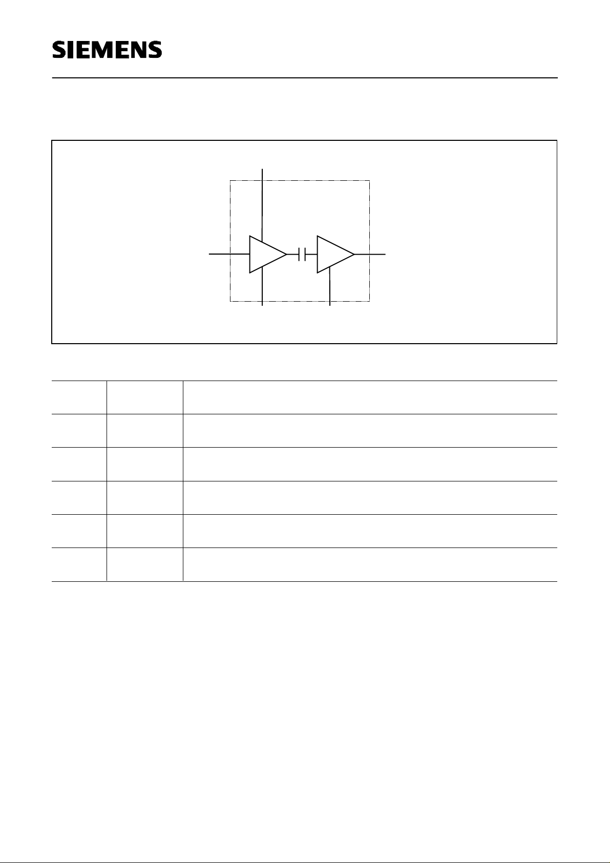
Functional Block Diagram
(3)
CGY 98
VD1
(1)
RFin/Vg
(2,5) (2,5)
GND
Pin # Configuration
1
2
3
4
RFin/VG
GND
VD1
RFout/VD2
RF input power + Gate voltage
RF and DC ground
Pos. drain voltage 1st stage
RF output power / Pos. drain voltage 2nd stage
GND
RFout
(4)
VD2
/
5
GSM-Operation
Siemens Aktiengesellschaft 2 12.03.1998
Semiconductor Group 2 1998-11-01
HL HFD PE GaAs
GND
RF and DC ground
 Loading...