

Siemens BSP280 Datasheet
IGBT Transistor BSP 280
Preliminary Data
● V
● I
● N channel
● MOS input (voltage-controlled)
● High switch speed
● Very low tail current
● Latch-up free
● Suitable freewheeling diode BAX 280
Type Ordering Code Tape and Reel
1000 V
CE
2.5 A
C
Information
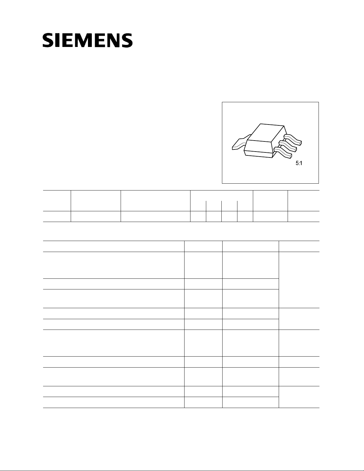
Pin Configuration Marking Package
1234
BSP 280 Q67000-S279 E6327: 1000 pcs/reel G C E C BSP 280 SOT-223
Maximum Ratings
Parameter Symbol Values Unit
Continuous collector current
T
Soldering point,
Continuous collector current ambient,
= 25 ˚C
S
T
= 80 ˚C
S
T
Pulsed collector current
T
Soldering point,
= 80 ˚C
S
Collector-emitter voltage
Gate-emitter voltage
Power dissipation
Soldering point,
Ambient
T
= 80 ˚C
S
T
= 25 ˚C
A
Operating and storage temperature range
Thermal resistance
1)
chip-ambient
chip-soldering point
= 80 ˚C I
A
I
C
C
I
C puls
V
V
P
T
R
R
CE
GE
tot
, T
j
thJA
thJS
stg
2.5
1.5
0.5
3.0
1000 V
± 20
10
1.8
– 40 … + 150 ˚C
70
6
A
W
K/W
DIN humidity category, DIN 40 040 – E –
IEC climatic category, DIN IEC 68-1 – 40/150/56
IGBT = Insulated Gate Bipolar Transistor
1)
Transistor on epoxy pcb 40 mm × 40 mm × 1.5 mm with 6 cm2 copper area for drain connection.
BSP 280
Electrical Characteristics
T
= 25 ˚C, unless otherwise specified.
at
j
Parameter Symbol Values Unit
min. typ. max.
Static Characteristics
Collector-emitter breakdown voltage
V
= 0, IC = 0.1 mA
GE
Gate threshold voltage
V
= VCE, IC = 0.1 mA
GE
Collector-emitter saturation voltage
V
= 15 V, IC = 0.5 A
GE
T
= 25 ˚C
j
T
= 125 ˚C
j
T
= 150 ˚C
j
V
= 15 V, IC = 1.5 A
GE
T
= 25 ˚C
j
T
= 125 ˚C
j
T
= 150 ˚C
j
Zero gate voltage collector current
V
= 1000 V, VGE = 0
CE
T
= 25 ˚C
j
T
= 125 ˚C
j
Gate-emitter leakage current
V
= 20 V, VCE = 0
GE
V
(BR)CES
V
GE(th)
V
CE(sat)
I
CES
I
GES
1000 – –
4.5 5.5 6.5
–
–
–
–
–
–
–
–
1.8
2.1
2.2
2.8
3.8
4.0
1
–
–
–
3.0
3.3
4.3
4.5
25
100
– 0.1 100
V
µA
nA
Dynamic Characteristics
Forward transconductance
V
= 20 V, IC = 1.5 A
CE
Input capacitance
V
= 0, VGE = 25 V, f = 1 MHz
CE
Output capacitance
V
= 0, VGE = 25 V, f = 1 MHz
CE
Reverse transfer capacitance
V
= 0, VGE = 25 V, f = 1 MHz
CE
Turn-on delay time
V
=600V,VGE =15V,R
CC
G(on)
Rise time
V
=600V,VGE =15V,R
CC
G(on)
=25Ω, IC =1.5A
=25Ω, IC =1.5A
g
C
C
C
t
d(on)
t
r
fs
iiss
oss
rss
S
– 0.6 –
pF
– 225 –
–25–
–13–
ns
–20–
–15–
 Loading...