

Siemens BSP171P Datasheet
BSP 171 P
DSIDRDS(on)
@ V
GS
jmax
AR
j(max)
AR
jmax
GS
tot
j
Preliminary data
SIPMOS Power Transistor
• P-Channel
• Enhancement mode
• Avalanche rated
• Logic Level
• dv/dt rated
Type V
BSP 171 P
-60 V -1.8 A 0.3 Ω VGS = -10 V P-SOT223-4-1-Q67041-S4019
Maximum Ratings, at Tj = 25 °C, unless otherwise specified
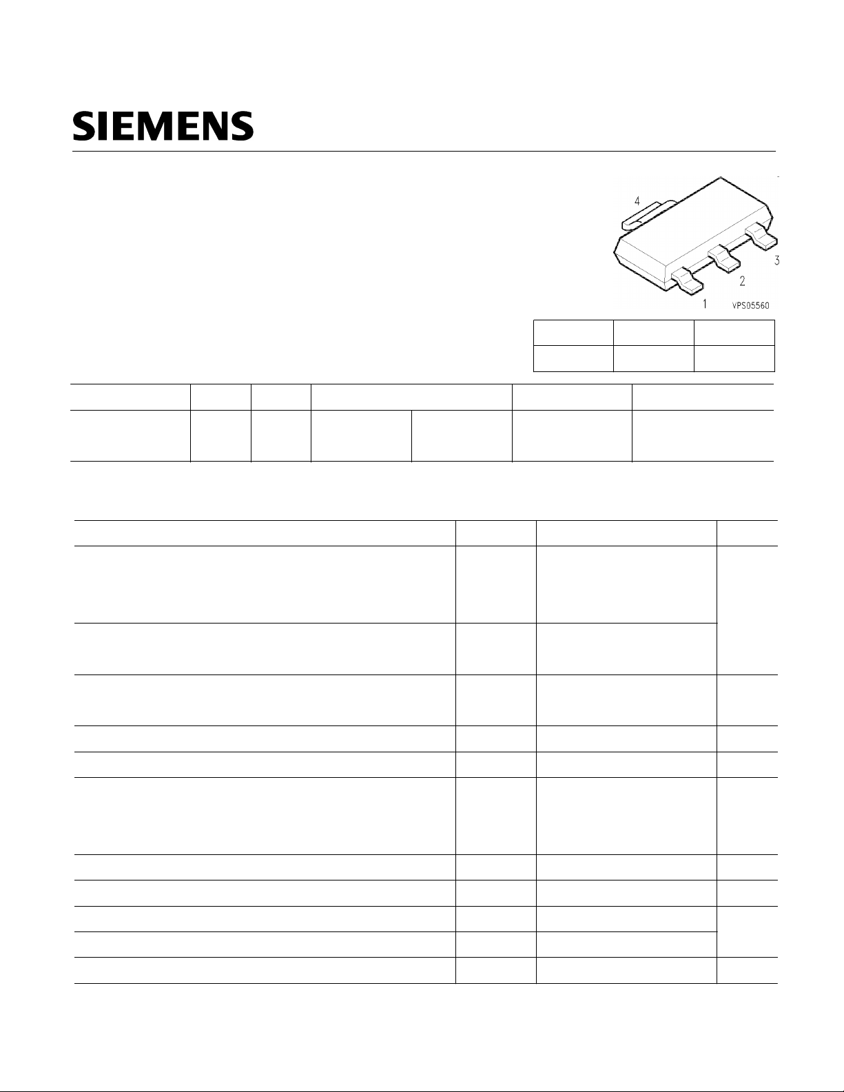
Pin 1 Pin2/4 Pin 3
G D S
Package Ordering Code
-
Continuous drain current
TA = 25 °C
TA = 100 °C
TA = 25 °C
ID = -1.8 A, VDD = -25 V, RGS = 25 Ω
Avalanche current,periodic limited by T
IS = -1.8 A, VDD ≤ V
T
= 150 °C
(BR)DSS
, di/dt = 100 A/µs,
Gate source voltage V
I
D
I
D puls
AS
I
E
Value UnitParameter Symbol
-1.8
-1.15
-7.2Pulsed drain current
70E
0.18 mJAvalanche energy,periodic limited by T
6
±14 V
1.8 WPower dissipation, TA = 25 °C P
A
mJAvalanche energy, single pulse
A-1.8
KV/µsdv/dtReverse diode dv/dt
°COperating temperature -55 ...+150T
Storage temperature T
Semiconductor Group 04 / 19981
stg
-55 ...+150
55/150/56IEC climatic category; DIN IEC 68-1

BSP 171 P
thJS
thJA
Preliminary data
Electrical Characteristics
at Tj = 25 °C, unless otherwise specified typ. max.min.
Thermal Characteristics
Thermal resistance, junction -soldering point (Pin 4) K/Wtbd
-SMD version, device on PCB:
@ min. footprint
@ 6 cm2 cooling areaF)
R
thJA
-
-
tbd
tbd
Static Characteristics
Drain- source breakdown voltage
(BR)DSS
- --60V
VGS = 0 V, ID = -0.25 mA
Gate threshold voltage, VGS = VDS
GS(th)
-1 -1.5V
ID = -460 µA, Tj = 25 °C
UnitValuesSymbolParameter
tbd-R
-Thermal resistance, junction - ambient R
-
70
V
-2
VDS = -60 V, VGS = 0 V, Tj = -40 °C
VDS = -60 V, VGS = 0 V, Tj = 25 °C
VDS = -60 V, VGS = 0 V, Tj = 150 °C
Gate-source leakage current
VGS = -20 V, VDS = 0 V
Drain-Source on-state resistance
VGS = -4.5 V, ID = -1.5 A
VGS = -10 V, ID = -1.8 A
I
DSS
GSS
R
DS(on)
-
-
-
-
-0.1
-
-0.1
-1
-100
µAZero gate voltage drain current
-10 -100 nA-I
-
-
0.3
0.21
0.45
0.3
Ω
Semiconductor Group 04 / 19982
 Loading...