

Siemens BFS483 Datasheet
BFS 483
NPN Silicon RF Transistor
• For low-noise, high-gain broadband amplifier
at colector current from 2mA to 28mA
•
f
= 8GHz
T
F = 1.2dB at 900MHz
• Two (galvanic) internal isolated
Transistors in one package
ESD: Electrostatic discharge sensitive device, observe handling precaution!
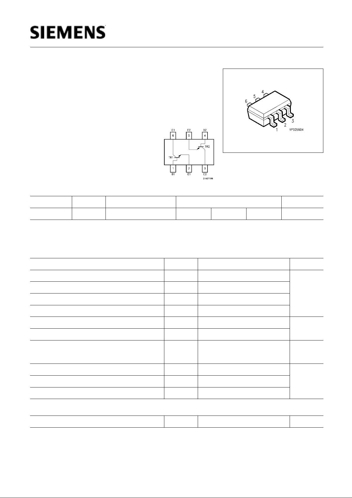
Type Marking Ordering Code Pin Configuration Package
BFS 483 RHs Q62702-F1574 1/4 = B 2/5 = E 3/6 = C SOT-363
data below is of a single transistor
Maximum Ratings
Parameter Symbol Values Unit
Collector-emitter voltage
Collector-emitter voltage
Collector-base voltage
Emitter-base voltage
Collector current
Base current
Total power dissipation
T
≤ 40 °C
S
Junction temperature
Ambient temperature
V
V
V
V
I
I
P
T
T
C
B
CEO
CES
CBO
EBO
tot
j
A
12 V
20
20
2
65 mA
5
mW
450
150 °C
- 65 ... + 150
Storage temperature
T
stg
- 65 ... + 150
Thermal Resistance
Junction - soldering point
1)
T
is measured on the collector lead at the soldering point to the pcb.
S
1)
R
thJS
≤ 245 K/W
Semiconductor Group 1 Dec-16-1996
BFS 483
Electrical Characteristics at
T
= 25°C, unless otherwise specified.
A
Parameter Symbol Values Unit
min. typ. max.
DC Characteristics
Collector-emitter breakdown voltage
I
= 1 mA,
C
I
B
= 0
Collector-emitter cutoff current
V
= 20 V,
CE
V
BE
= 0
Collector-base cutoff current
V
= 10 V,
CB
I
E
= 0
Emitter-base cutoff current
V
= 1 V,
EB
I
C
= 0
DC current gain
I
= 15 mA,
C
V
CE
= 8 V
V
(BR)CEO
I
CES
I
CBO
I
EBO
h
FE
V
12 - -
µA
- - 100
nA
- - 100
µA
- - 1
-
50 100 200
Semiconductor Group 2 Dec-16-1996
 Loading...