

NPN Silicon Double Transistors BCV 61
Preliminary Data
● To be used as a current mirror
● Good thermal coupling and VBE matching
● High current gain
● Low emitter-saturation voltage
Type Ordering Code
Marking
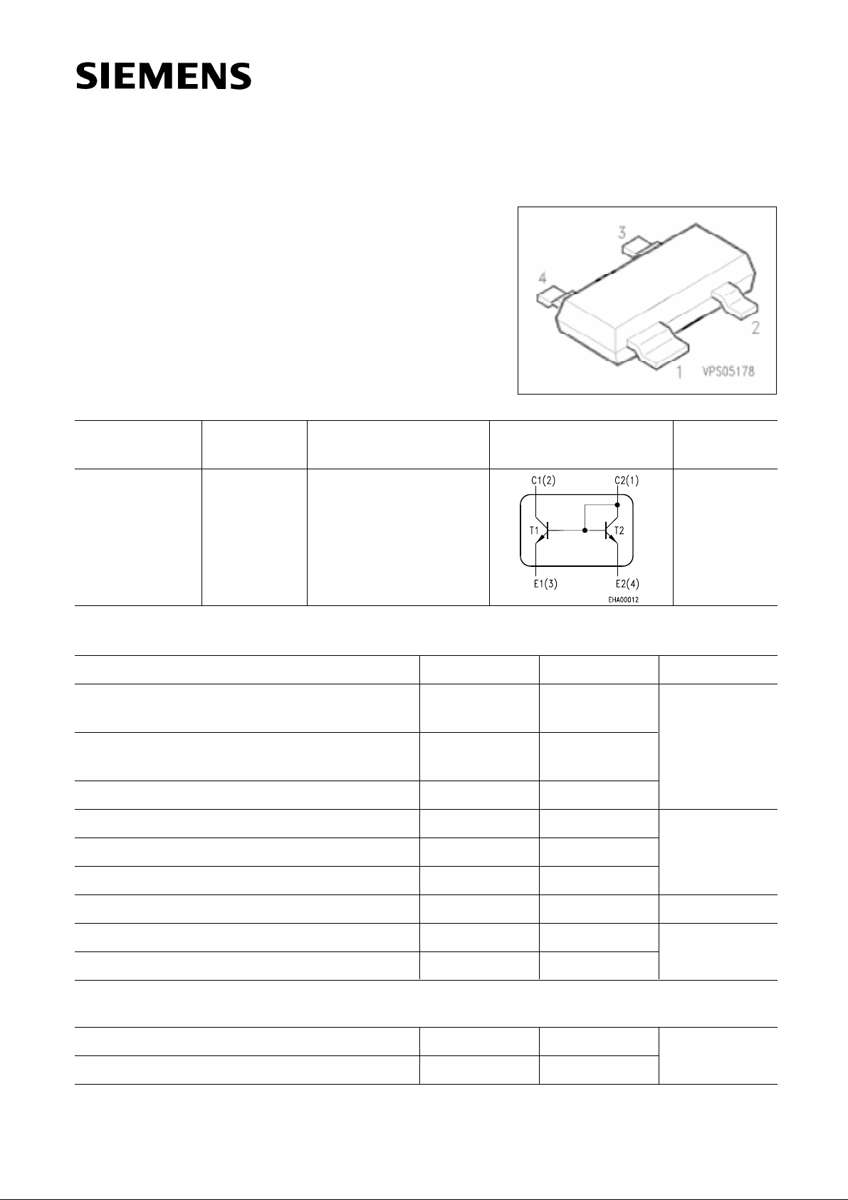
Pin Configuration
Package
(tape and reel)
BCV 61 A
BCV 61 B
BCV 61 C
1Js
1Ks
1Ls
Q62702-C2155
Q62702-C2156
Q62702-C2157
SOT-143
Maximum Ratings
Parameter Symbol Values Unit
Collector-emitter voltage
CE0 30 V
V
(transistor T1)
Collector-base voltage (open emitter)
VCB0 30
(transistor T1)
Emitter-base voltage VEBS 6
Collector current IC 100 mA
1)
Collector peak current ICM 200
Base peak current (transistor T1) IBM 200
Total power dissipation, T
S ≤ 99 ˚C
2)
Ptot 300 mW
Junction temperature Tj 150 ˚C
Storage temperature range T
stg – 65 … + 150
Thermal Resistance
Junction - ambient
2)
Junction - soldering point R
1)
For detailed information see chapter Package Outlines.
2)
Package mounted on epoxy pcb 40 mm × 40 mm × 1.5 mm/6 cm2 Cu.
Semiconductor Group 1
Rth JA ≤ 240 K/W
th JS ≤ 170
5.91
Electrical Characteristics
I
I
I
I
I
I
I
I
I
I
I
A = 25 ˚C, unless otherwise specified.
at T
DC characteristics for transistor T1
BCV 61
UnitValuesParameter Symbol
min. typ. max.
V
(BR)CE0 30 – –
C = 10 mA, IB = 0
Collector-base breakdown voltage
C = 10 µA, IB = 0
Emitter-base breakdown voltage
E = 10 µA, IC = 0
Collector-base cutoff current
CB = 30 V, IE = 0
V
CB = 30 V, IE = 0, TA = 150 ˚C
V
DC current gain
C = 0.1 mA, VCE = 5 V
C = 2 mA, VCE = 5 V BCV 61 A
1)
BCV 61 B
BCV 61 C
Collector-emitter saturation voltage
C = 10 mA, IB = 0.5 mA
C = 100 mA, IB = 5 mA
Base-emitter saturation voltage
C = 10 mA, IC = 0.5 mA
C = 100 mA, IC = 5 mA
1)
1)
V
(BR)CB0 30 – –
V
(BR)EBS 6––
CB0
I
V
V
–
–
100
110
200
420
CEsat
–
–
BEsat
–
–
–
–
–
180
290
520
90
200
700
900
15
5
220
450
800
250
600
–
–
VCollector-emitter breakdown voltage
nA
µA
–hFE
mV
Base-emitter voltage
C = 2 mA, VCE = 5 V
C = 10 mA, VCE = 5 V
BE
V
580
–
660
–
700
770
1)
Pulse test conditions: t ≤ 300 µs, D = 2 %.
Semiconductor Group 2
Electrical Characteristics
I
I
I
I
I
I
I
I
A = 25 ˚C, unless otherwise specified.
at T
DC characteristics for transistor T2
BCV 61
UnitValuesParameter Symbol
min. typ. max.
VBase-emitter forward voltage
E = 10 µA
E = 250 mA
BES
V
0.4
–
–
–
–
1.8
–Matching of transistor T1 and transistor T2
E2 = 0.5 mA and VCE1 = 5 V
at I
A = 25 ˚C
T
A = 150 ˚C
T
I
C1 / IC2
IC1 / IC2
0.7
0.7
–
–
1.3
1.3
IE2 –5–
mAThermal coupling of transistor T1 and
transistor T21) T1: VCE = 5 V
Maximum current for thermal stability of I
C1
AC characteristics for transistor T1
C = 10 mA, VCE = 5 V, f = 100 MHz
CB = 10 V, IC = iC = 0, f = 1 MHz
V
Input capacitance
EB = 0.5 V, IC = iC = 0, f = 1 MHz
V
f
T – 250 –
C
cb –3–
C
ibo –8–
MHzTransition frequency
pFCollector-base capacitance
F –2–
C = 200 µA, VCE = 5 V, RS = 2 kΩ
dBNoise figure
f= 1 kHz, B = 200 Hz
h
C = 1 mA, VCE = 10 V, f = 1 kHz
Open-circuit reverse voltage transfer ratio
C = 1 mA, VCE = 10 V, f = 1 kHz
C = 1 mA, VCE = 10 V, f = 1 kHz
C = 1 mA, VCE = 10 V, f = 1 kHz
11e – 4.5 –
h
12e –2–
h
21e 100 – 900
h
22e –30–
kΩInput impedance
10
–Short-circuit forward current transfer ratio
µSOpen-circuit output admittance
–4
1)
Without emitter resistor. Device mounted on alumina 15 mm × 16.5 mm × 0.7 mm.
Semiconductor Group 3
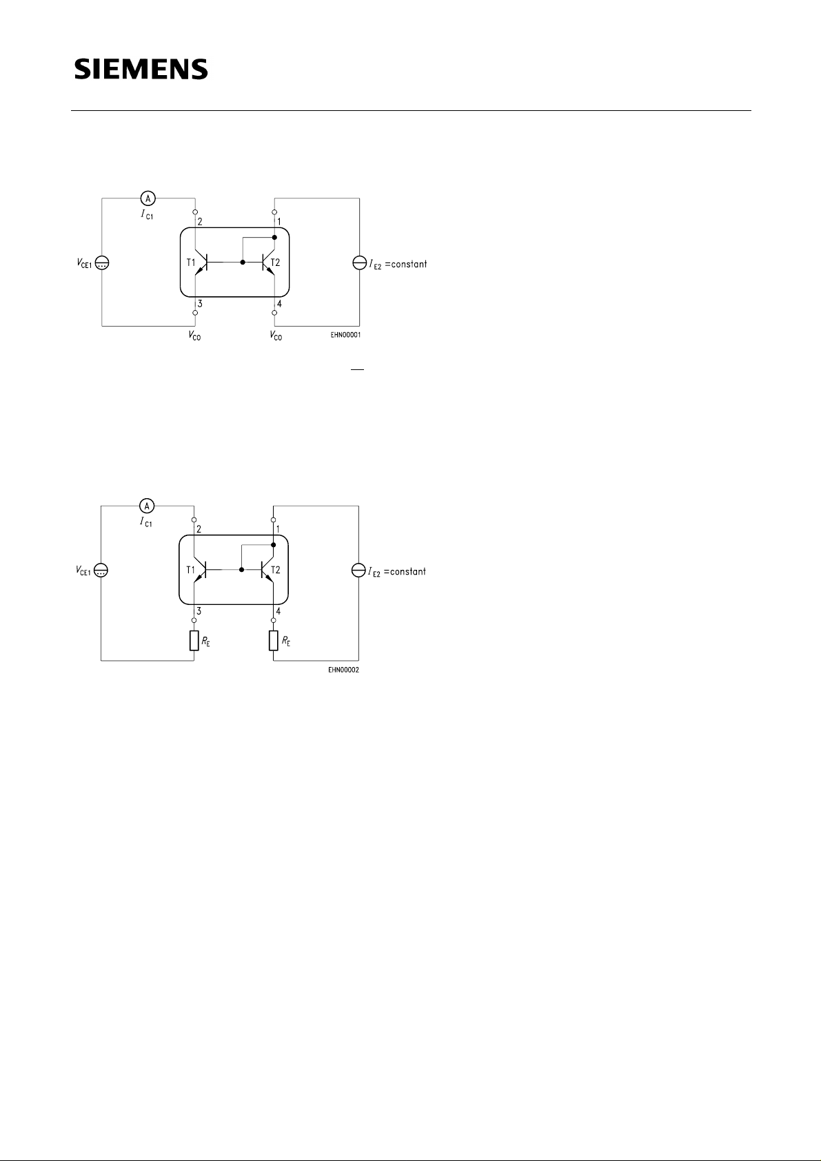
Test circuit for current matching
BCV 61
Note: Voltage drop at contacts: VCO < VT = 16 mV
Characteristic for determination of V
condition of I
C1 / IE2 = 1.3
2
3
CE1 at specified RE range with IE2 as parameter under
Note: BCV 61 with emitter resistors
Semiconductor Group 4

BCV 61
Total power dissipation Ptot = f (TA*; TS)
* Package mounted on epoxy
Permissible pulse load Ptot max/Ptot DC = f (tp)
Semiconductor Group 5
 Loading...