

Siemens BCV47, BCV27 Datasheet
NPN Silicon Darlington Transistors BCV 27
BCV47
● For general AF applications
● High collector current
● High current gain
● Complementary types: BCV 26, BCV 46 (PNP)
Type Ordering Code
BCV 27
BCV 47
Marking
FFs
FGs
(tape and reel)
Q62702-C1474
Q62702-C1501
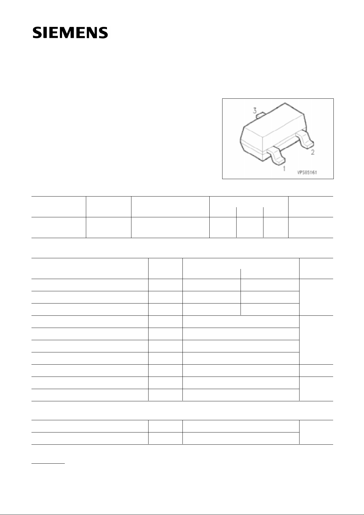
Pin Configuration
1 2 3
B E C
Package
SOT-23
Maximum Ratings
Parameter Symbol Values Unit
BCV 27 BCV 47
Collector-emitter voltage V
Collector-base voltage VCB0
Emitter-base voltage V
Collector current IC mA
Peak collector current ICM
CE0 V
30 60
40 80
EB0
10 10
500
800
Base current IB 100
Peak base current I
Total power dissipation, T
S = 74 ˚C Ptot mW
BM 200
360
1)
Junction temperature Tj ˚C
Storage temperature range T
stg
150
– 65 … + 150
Thermal Resistance
Junction - ambient
2)
Rth JA ≤ 280 K/W
Junction - soldering point Rth JS ≤ 210
1)
For detailed information see chapter Package Outlines.
2)
Package mounted on epoxy pcb 40 mm × 40 mm × 1.5 mm/6 cm2 Cu.
Semiconductor Group 1
5.91
Electrical Characteristics
I
I
I
I
I
I
I
I
I
A = 25 ˚C, unless otherwise specified.
at T
DC characteristics
BCV 27
BCV 47
UnitValuesParameter Symbol
min. typ. max.
(BR)CE0
V
C = 10 mA
BCV 27
BCV 47
Collector-base breakdown voltage
C = 100 µA
BCV 27
(BR)CB0
V
BCV 47
30
60
40
80
–
–
–
–
–
–
–
–
VCollector-emitter breakdown voltage
Emitter-base breakdown voltage, IE = 10 µA V(BR)EB0 10 – –
Collector cutoff current
VCB = 30 V BCV 27
CB = 60 V BCV 47
V
CB = 30 V, TA = 150 ˚C BCV 27
V
CB = 60 V, TA = 150 ˚C BCV 47
V
I
CB0
–
–
–
–
–
–
–
–
100
100
10
10
nA
nA
µA
µA
nAEmitter cutoff current, VEB = 4 V IEB0 – – 100
DC current gain
C = 100 µA, VCE = 1 V BCV 27
C = 10 mA, VCE = 5 V BCV 27
C = 100 mA, VCE = 5 V BCV 27
C = 0.5 A, VCE = 5 V BCV 27
Collector-emitter saturation voltage
C = 100 mA, IB = 0.1 mA
Base-emitter saturation voltage
C = 100 mA, IB = 0.1 mA
1)
BCV 47
BCV 47
BCV 47
BCV 47
1)
1)
4000
2000
10000
4000
20000
10000
4000
2000
VCEsat ––1
VBEsat – – 1.5
–
–
–
–
–
–
–
–
–
–
–
–
–
–
–
–
–hFE
V
AC characteristics
C = 50 mA, VCE = 5 V, f = 20 MHz
CB = 10 V, f = 1 MHz
V
1)
Pulse test: t ≤ 300µs,D = 2 %.
Semiconductor Group 2
f
T – 170 –
C
obo – 3.5 –
MHzTransition frequency
pFOutput capacitance
 Loading...