

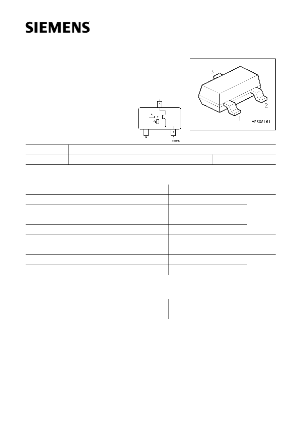
BCR 112
NPN Silicon Digital Transistor
• Switching circuit, inverter, inferface circuit,
driver circuit
• Built in bias resistor (R1=4.7kΩ, R2=4.7kΩ)
Type Marking Ordering Code Pin Configuration Package
BCR 112 WFs Q62702-C2254 1 = B 2 = E 3 = C SOT-23
Maximum Ratings
Parameter Symbol Values Unit
Collector-emitter voltage
Collector-base voltage
Emitter-base voltage
Input on Voltage
DC collector current
Total power dissipation,
Junction temperature
Storage temperature
T
= 102°C
S
V
V
V
V
I
P
T
T
C
CEO
CBO
EBO
i(on)
tot
j
stg
50 V
50
10
15
100 mA
200 mW
150 °C
- 65 ... + 150
Thermal Resistance
Junction ambient
1)
Junction - soldering point
1) Package mounted on pcb 40mm x 40mm x 1.5mm / 6cm2 Cu
R
R
thJA
thJS
≤
350 K/W
≤
240
Semiconductor Group
1 Nov-26-1996

BCR 112
Electrical Characteristics at
T
=25°C, unless otherwise specified
A
Parameter Symbol Values Unit
min. typ. max.
DC Characteristics
Collector-emitter breakdown voltage
I
= 100 µA,
C
I
B
= 0
Collector-base breakdown voltage
I
= 10 µA,
C
I
B
= 0
Collector cutoff current
V
= 40 V,
CB
I
E
= 0
Emitter cutoff current
V
= 10 V,
EB
I
C
= 0
DC current gain
I
= 5 mA,
C
V
CE
= 5 V
V
(BR)CEO
V
(BR)CBO
I
CBO
I
EBO
h
FE
V
50 - -
50 - -
nA
- - 100
mA
- - 1.61
-
20 - -
Collector-emitter saturation voltage 1)
I
= 10 mA,
C
I
= 0.5 mA
B
Input off voltage
I
= 100 µA,
C
V
CE
= 5 V
Input on Voltage
I
= 2 mA,
C
V
CE
= 0.3 V
Input resistor
Resistor ratio
AC Characteristics
Transition frequency
I
= 10 mA,
C
V
= 5 V, f = 100 MHz
CE
Collector-base capacitance
V
= 10 V, f = 1 MHz
CB
1) Pulse test: t < 300µs; D < 2%
V
CEsat
V
i(off)
V
i(on)
R
1
R
1
f
T
C
cb
V
- - 0.3
0.8 - 1.5
1 - 2.5
3.2 4.7 6.2 k
/
R
2
0.9 1 1.1 -
Ω
MHz
- 140 pF
- 3 -
Semiconductor Group
2 Nov-26-1996
BCR 112
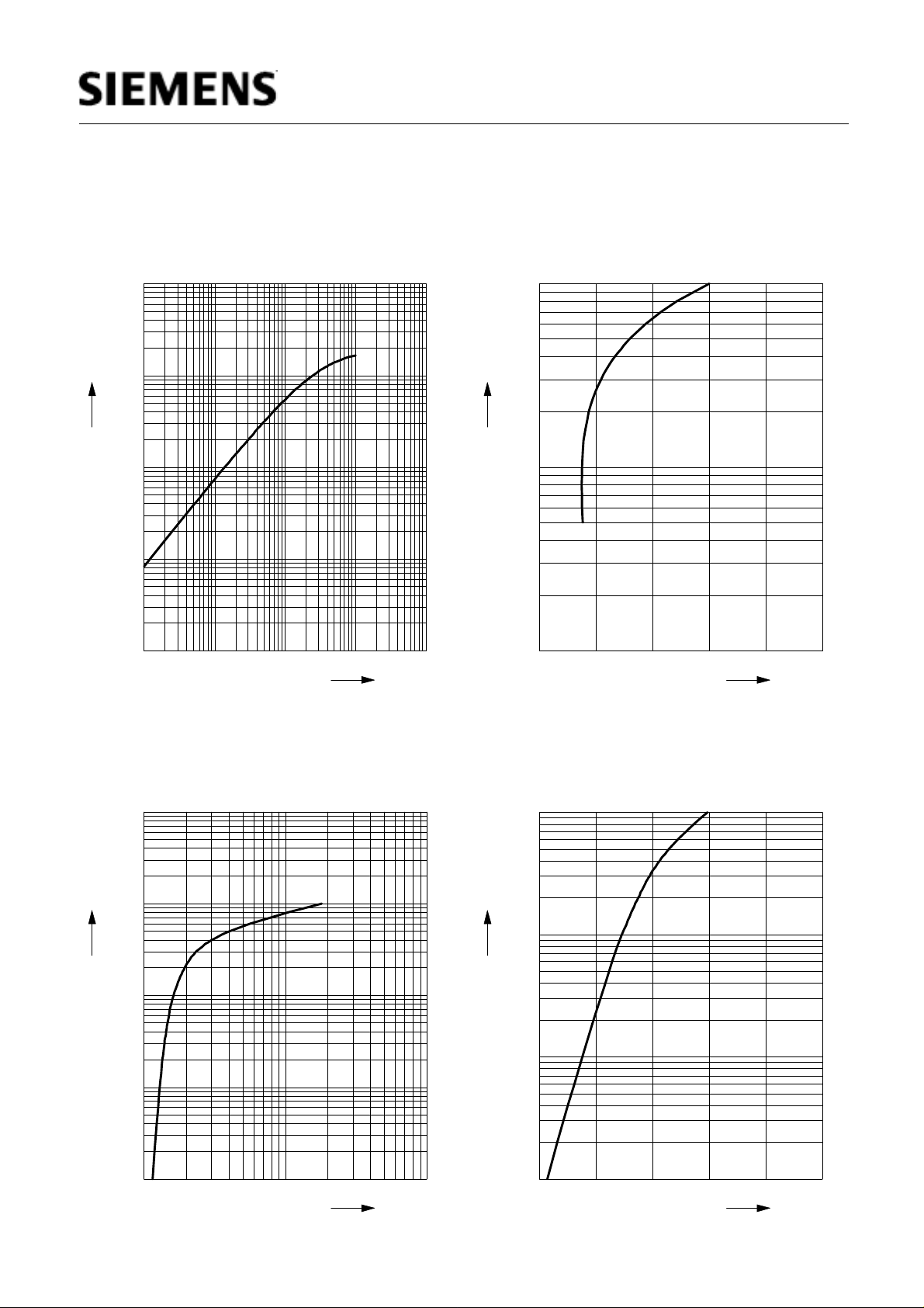
DC Current Gain
V
= 5V (common emitter configuration)
CE
h
=
f (I
FE
)
C
3
10
-
h
FE
2
10
1
10
0
10
Collector-Emitter Saturation Voltage
V
I
C
CEsat
10
mA
10
= f(
2
1
I
),
h
FE
= 20
C
-1
10
-1
10
Input on Voltage
V
= 0.3V (common emitter configuration)
CE
10
0
V
i(on)
1
10
= f(
I
)
C
10 2 mA
3
10
mA
I
C
2
10
1
10
0
10
0
10
I
C
Input off voltage
V
0.0 0.1 0.2 0.3 V 0.5
V
= f(
I
i(off)
= 5V (common emitter configuration)
CE
)
C
V
CEsat
1
10
mA
I
C
0
10
-1
10
-1
10
0
10
Semiconductor Group
10
-2
1
V
V
i(on)
10
1.0 1.2 1.4 1.6 V 2.0
V
i(off)
3 Nov-26-1996
BCR 112
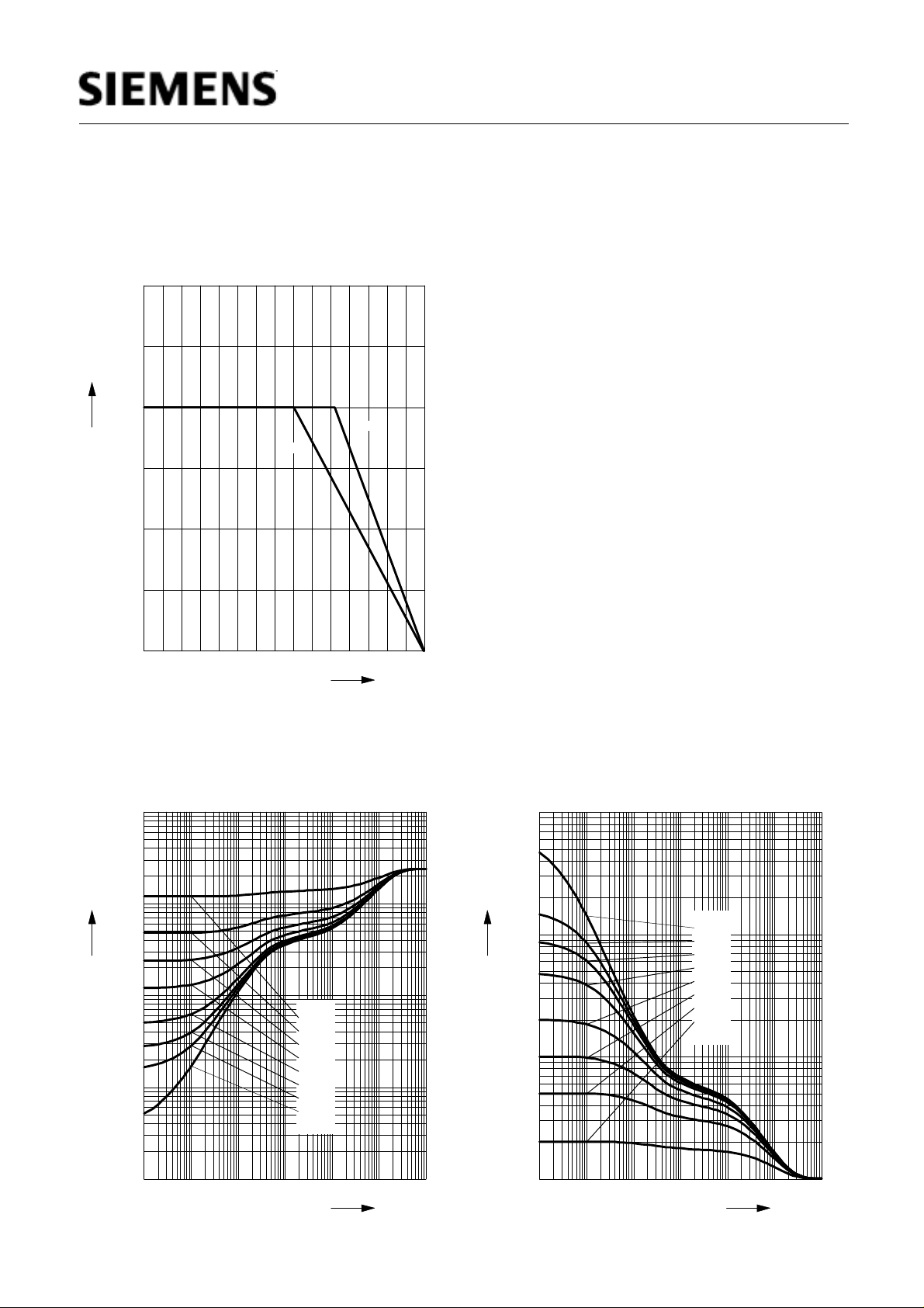
Total power dissipation
P
tot
* Package mounted on epoxy
300
mW
P
tot
200
T
A
150
100
50
= f (
T
*;
T
)
A
S
T
S
0
0 20 40 60 80 100 120 °C 150
Permissible Pulse Load
3
10
K/W
R
thJS
2
10
1
10
0
10
R
thJS
0.5
0.2
0.1
0.05
0.02
0.01
0.005
D = 0
= f(
TA,T
S
t
)
p
Permissible Pulse Load
P
totmax
/
P
totDC
= f(
t
)
p
3
10
-
P
/
P
totDC
10
10
2
1
D = 0
0.005
0.01
0.02
0.05
0.1
0.2
0.5
totmax
-1
10
10
-6
10
-5
Semiconductor Group
10
0
-4
10
-3
-2
10
10
-1
t
p
0
10
s
10
10
-6
10
-5
10
-4
10
-3
10
-2
10
-1
t
p
0
10
s
4 Nov-26-1996
 Loading...