

Siemens BB112 Datasheet

Semiconductor Group 1
BB 112
Silicon Variable Capacitance Diode BB 112
● For AM tuning applications
● Specified tuning range
1 … 8.0 V
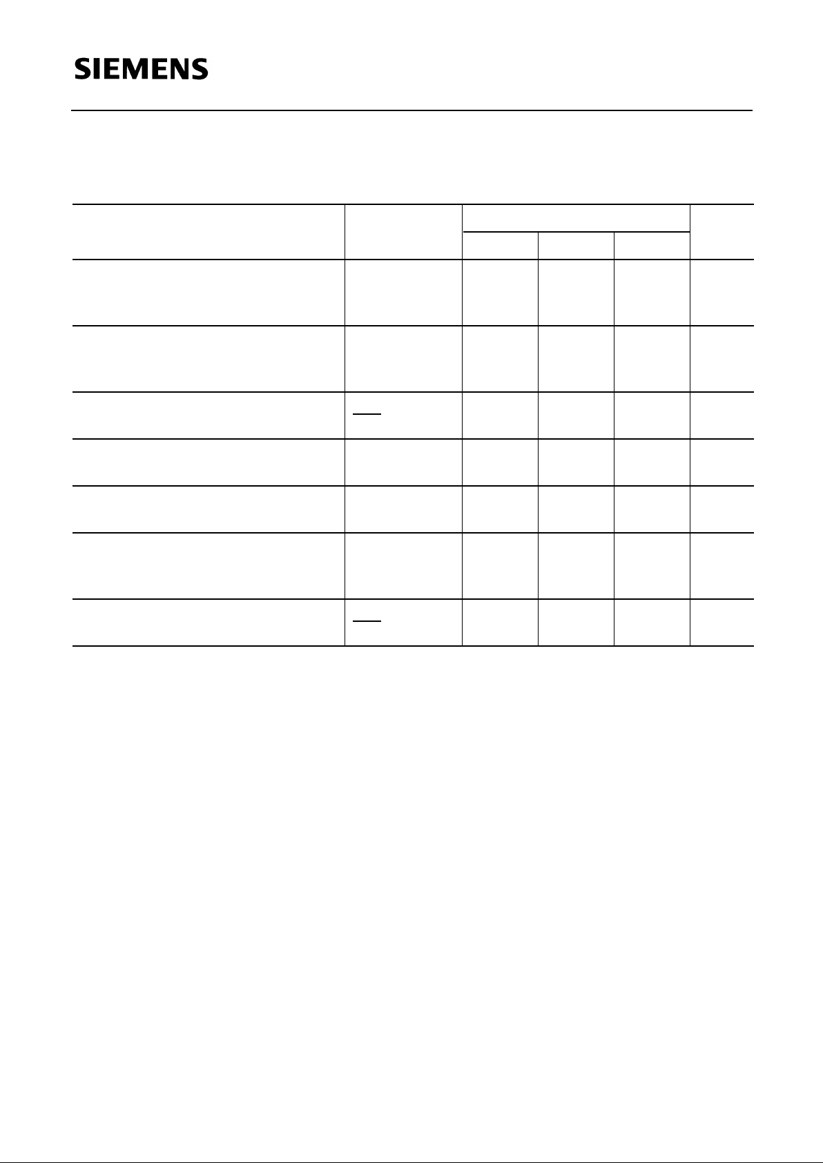
Maximum Ratings
Type Ordering CodeMarking
Package
1)
Pin Configuration
BB 112 Q62702-B240– TO-92
Parameter Symbol Values Unit
Reverse voltage V
R 12 V
Forward current,
T
A ≤ 60 ˚C IF 50 mA
Operating temperature range T
op – 55 … + 85 ˚C
1)
For detailed information see chapter Package Outlines.
07.94
Semiconductor Group 2
BB 112
Electrical Characteristics
at T
A = 25 ˚C, unless otherwise specified.
Parameter Symbol
min. typ.
UnitValues
max.
Reverse current
V
R = 10 V
V
R = 10 V, TA = 60 ˚C
I
R nA
–
–
–
–
50
200
Diode capacitance, f = 1 MHz
V
R = 1 V
V
R = 8 V
C
T pF
440
17.5
470
–
520
34
Capacitance ratio
V
R = 1 V, 8 V
C
T1
CT8
–15 – –
Series resistance
V
R = 1 V, f = 0.5 MHz
r
s Ω– 1.4 –
Q factor
V
R = 1 V, f = 0.5 MHz
Q –– 480 –
Temperature coefficient
of diode capacitance
V
R = 1 V, f = 1 MHz
TC
C ppm/K– 500 –
Capacitance matching
V
R = 1 … 8 V
∆CT
CT
%––3
 Loading...