

Page 1

SIEMENS
Page 2

SIEMENS
Floppy Disk Drive FDD 100-8
INTRODUCTION
OPERATION
THEORY OF OPERATION
INSTALLATION
Technical Manual
Volume 1 Model 100-8D
Page 3
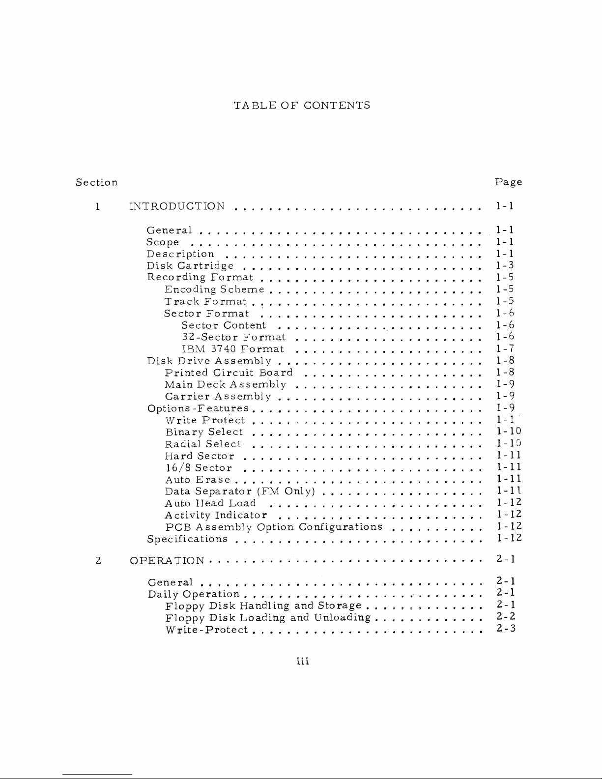
TABLE OF CONTENTS
1 IN T R O D U C TIO N .................................................................................................... 1-1
General .................................................................................................................. 1-1
Scope ..................................................................................................................... 1-1
De sc ription ....................................................................................................... 1-1
Disk C a r t r i d g e ................................................................................................ 1-3
Recording F o r m a t ......................................................
...
...............................
1-5
Encoding S c h e m e ......................
...
............................................................ 1-5
Trac k F o r m a t ............................................................................................. 1-5
Sector Fo r m at
.........................
...
............................................................ 1-6
Sector Content .................................................................................. 1-6
32-Sector F o r m a t ........................................................................... 1-6
IBM 37 40 Form at ........................................................................... 1-7
Disk Drive A s s e m b l y .................................................................................. 1-8
Printed Circuit Board .............................................................
...
1-8
Main Deck A s s e m b l y ........................................................................... 1-9
C a rrier A s s e m b ly .................................................................................. 1-9
Options-F ea tu r e s
.........................
...
.................
...
.................
...
..................... 1-9
Write P r o t e c t ............................................................................................. 1-1
Binary Select
. . . . . . .
................................
. ............................. 1-10
Radial Select ............................................................................................. 1-10
Hard S e c t o r ................................................................................................ 1-11
16/8 Sector ................................................................................................ 1-11
Auto E ra s e .................................................................................................... 1-11
Data Se parator (FM O n l y )
..................
...
...............................
...
1-11
Auto Head Load .......................................
...
1-12
Activity Indicator .................................................................................. 1-12
PC B A ssem bly Option C o n fig u r atio n s .................................... 1-12
Sp e cifi c a tio n s......................................................................................
...
1-12
2 O P E R A TIO N
................................
.............................................................................. 2-1
Gene r a l ......................................................................................
...
........................
2-1
Daily O p er a tio n ................................................................................................ 2-1
Floppy Disk Handling and S to ra g e ............................................... 2-1
Floppy Disk Loading and U nlo ad in g
...............
...
2-2
W rit e - P r o t e c t
.............................
...
............................................................ 2-3
ILL
Section Page
Page 4
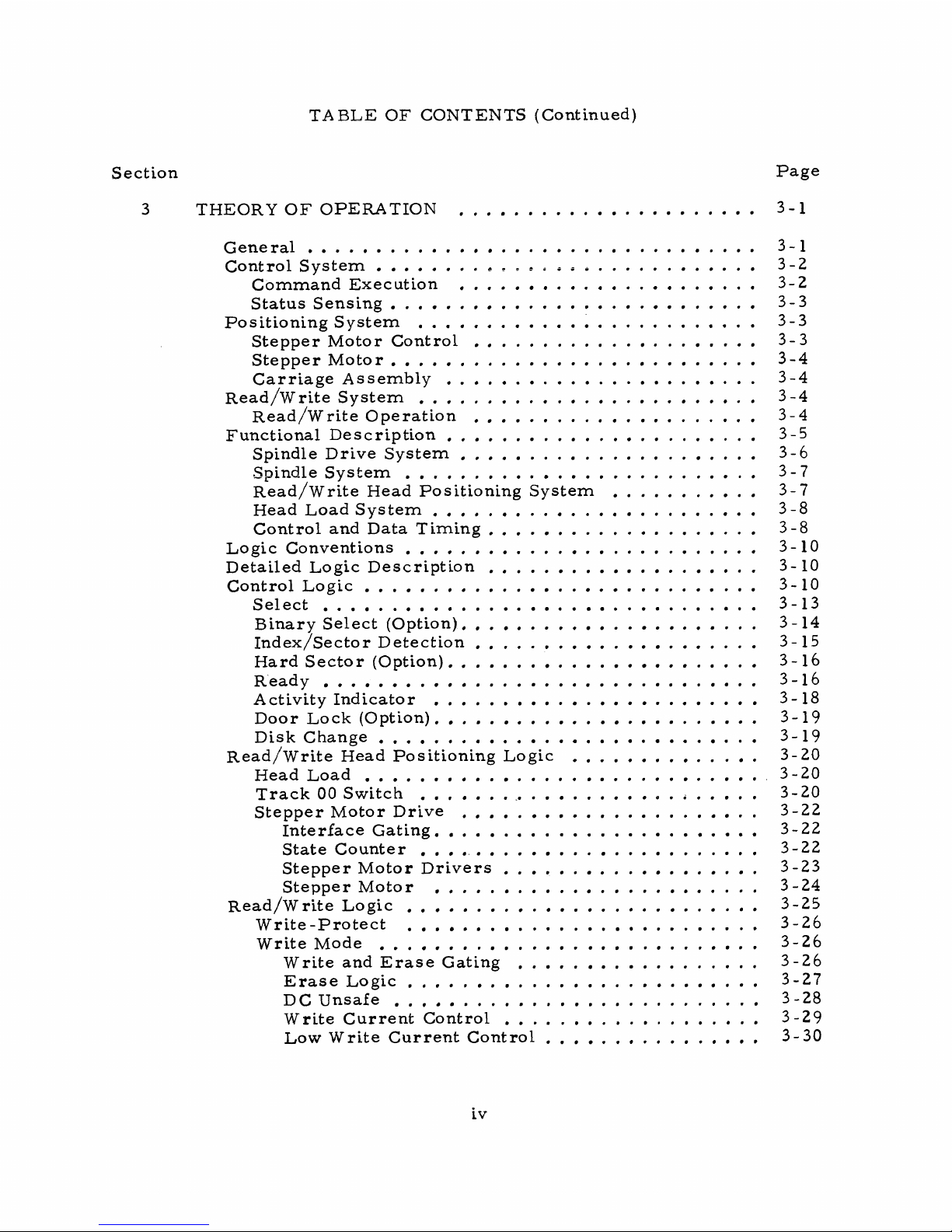
TABLE OF CONTENTS (Continued)
3 THEORY OF OPERATION
........................................................................ 3-1
G e n e r a l.............................................................................................................. 3-1
Control S y s te m
.....................
...
. .
....................................................... 3-2
Command Execution
..................
...
................................................... 3-2
Status S e n sin g .......................................................................................... 3-3
Positioning System ................................................................................... 3-3
Stepper Motor C o n t r o l .......................................................
...
3-3
Stepper M o t o r .......................................................................................... 3-4
Carriage A s s e m b l y ............................................................................ 3-4
Read/W rite S y s t e m ................................................................................... 3-4
Read/Write Operation ..................................................................... 3-4
Functional D es c r ip t i o n ............................................................................ 3-5
Spindle Drive S y s t e m
........................................................................ 3-6
Spindle System ...............................
«............................................ 3-7
Read/W rite Head Positioning System ................................... 3-7
Head Load S y s t e m
............................................................................... 3-8
Control and Data T i m in g .................................................................. 3-8
Logic Con v ention s
..............
...
.................................................................... 3-10
Detailed Logic D e s c r i p tio n ................................................................. 3-10
Control L o g i c ................................................................................................ 3-10
Select ............................. ........................................................................... 3-13
Binary Select (Option)........................................................................ 3-14
Index/Sector D e t e c t i o n ..................................................................... 3-15
Hard Secto r (Option)............................................................................ 3-16
Ready ...............................
...
..........................................................
...
3 - 16
Activity Indicator ..................
...
.......................................................... 3-18
Door Lock (Option)
..............
...
............................................................. 3-19
Disk C h a n ge .............................................
...
3-19
Read /W rite Head Positioning Logic
............................................. 3-20
Head L o a d ................................................................................................ 3-20
Track 00 Switch ..............................................................
...
.................
3-20
Stepper Motor Drive ......................................................................... 3-22
Interface Gating. ...........................................................
...
3-22
State Counter ................................................................................... 3-22
Stepper Motor D river s .............................................................. 3-23
Stepper Motor ............................................................................... 3-24
Read/W rite L o g i c ...................................................................................... 3-25
Write-Protect . .................................................
...
3-26
Write Mode ............................................................................................. 3-26
Write and E rase Gating .......................................................... 3-26
Erase L o g i c .......................................................
...
...........................
3-27
DC U n s a f e .......................................................................................... 3-28
Write Current Control .............................................................. 3-29
Low Write Current C o n t r o l
...............................
...
................. 3-30
Section Page
iv
Page 5
TABLE OF CONTENTS (Continued)
3 THEORY O F OPERATION (Continued)
Read M o d e ......................
...
.......................................................................... 3-31
Read/W rite S e l e c t ........................................................................... 3-32
Read LSI Circuit, Read Amplifier, and Filt e r . . . 3-32
Differentiating Network
..................
...
. e . s s « ................ 3-34
Crosso v e r Detector ....................................................................... 3-35
Time Domain Filter .................................................................... 3-35
FM Data Separator (Option)............................................................. 3-36
Term inating R e sistor Network . ............................................... 3-37
4 INS T A L LA TION....................................................................................................................... 4-1
G e n e r a l
................................................................
...
.............................................. 4-1
Inspection
............................................................................................
...
4-1
Unpacking
.........................
...
.............................................................................. 4-1
Mechanical Checks .............................................................'
.......................
4-2
Connecting C a b l e s ...............
...
.....................................................
...
4-2
AC Po w er C a b l e ...................................................................................... 4-4
DC Power C a b l e ...................................................................................... 4-5
Interface Signal Cable ...............
...
.................
...
................................ 4-5
Interface Signal Descriptions ...............
...
...................................
...
. 4-6
Logic Levels and T e r m in a t io n ...................................................... 4-6
Input S i g n a ls................................................................................................ 4-8
Output S i g n a ls............................................................................................. 4-8
Interface T i m i n g
.......................................
...
.................................................
4-8
Sy stem C o n fig ura t io n s
.......................................
...
................................... 4-12
Single-Drive C o n fig u ra t i o n ............................................................. 4-12
Radial Sele ct......................................................................................... 4-12
Daisy-Chained Radial S e l e c t .................................................. 4-13
Binary S e l e c t
..............
...
...............................
...
...............................
4-14
Interfac e/Intern al Options Installation ........................................... 4-16
Radial Select
................................
...
........................................................ 4-16
Binary Select" ...........................................
...
.............................................. 4-18
Radial S t e p ...............
...
................................................................................. 4-18
Radial Ready
.......................................
...
4-19
Ready Option ............................................................................................. 4-20
Radial I n d e x /S e c to r
...............
...
............................................................ 4-20
Radial Head Load O p tio n .................................................................... 4-20
Auto Head Load O p ti o n .............................
...
.....................
...
4-21
Hard S e c t o r
..............................................
...
.............................................
4-22
16 or 8 Sector ..................
...
................................................................... 4-22
Activity Indicator S e l e c t...........................................
...
.................
...
4-22
FM Data S e p arato r . . ..................
...
.................................................
4-23
Section Page
v
Page 6
TABLE OF CONTENTS (Continued)
4 INSTALLATION (Continued)
Tunnel-Erase Option ......................................
...
........................
...
4-23
Write P r otect O p ti o n
..............................................................
...
4-23
Disk Change Option ............................................................................ 4-24
Pha se O p t i o n .......................................................
...
..............................
4-24
Installation .................................................................................................... 4-25
Mounting D im e n sio n s
........................................................................ 4-25
Section Page
vi
Page 7

LIST OF ILLUSTRATIONS
Figure Page
1-1 Floppy Disk Drive Model F D D 1 0 0 - 8 D
1-2 Floppy Disk and Protective Envelope
..............................................
..............................................
1-1
1-3
1-3 Single and Double Density Encoding .................................................. 1-5
1-4 32-Sector F o r m a t ..............................
... .
........................................
...
1-6
1-5 IBM 3740 F orm at ........................................................................................... 1-7
1-6 Physical Dim ensions and Mounting p r o v i s i o n s
2-1 Floppy Disk and Storage Envelope
..............
..........................
. . . .
.......................
1-16
2-2
2-2 Floppy Disk Loading .................................................................................... 2-3
3-1 Floppy Disk D r i v e, Simplified Block Diagram
3-2 Detailed Functional Block D i a g ra m
3-3 Spindle Drive S y s t e m
...................
..................................................... 3-5
...
............................................................. 3-6
..........................
3-1
3-4 Spindle S y s t e m .................................................................................................. 3-7
3-5 Read/W rite Head Positioning S ystem ............................................... 3-8
3-6 Control and Data T im in g .............................................................................. 3-9
3-7 Interface Logic L e v e l s .....................................................
...
.......................
3-10
3-8 Logic S y m b o lo g y .............................................................................................. 3-11
3-9 Select L o g i c ......................................................................................................... 3-13
3-10 Index D etection Logic ................................................................................ 3-15
3-11 Index Timing ..................................................................................................... 3-lo
3-12 Hard Sector and 16/8 Sector Option L o g i c
....................................
3-17
3-13 INDEX/SECTOR T i m i n g .............................................................................. 3-17
3-14 Ready L o g i c ........................................................................................
...
3-18
3-15 Head Load L o g ic ............................................................................................... 3-19
3-16 Track 00 L o g ic
...................
...
.......................................................................... 3-21
3-17 Track 00 Timing .............................................................................................. 3-21
3-18 Stepper Motor Interface Gating L o g ic ............................................... 3-22
3-19 Stepper Motor Timing ................................................................................. 3-23
3-20 Stepper Motor Drivers Logic ................................................................ 3-24
3-21 Write Initiate T i m in g
3-22 W rite -P r o tect Logic .........................................................
3-23 Write and E rase Gating L o g ic
........................
................
...
.................* .................................. 3-25
...
...
.................
.......................
... .
....................
3-26
3-27
3-24 E rase L o g i c ......................................................................................................... -*-28
3-25 Erased Data P a t t e r n
3-26 DC Unsafe L o g i c .................................................................................
3-27 Write Current Control L ogic . . . . . .
........................
...
....................
..............................
... .
....................
...
. 3-29
...
3-29
...
3-30
vii
Page 8
LIST OF ILLUSTRATIONS (Continued)
Figure Page
3-28 Write Current S w i tch in g
............................................................................ 3-31
3-29 Write Current Timing ................................................................................ 3-32
3-30 Read Initiate Timing .................................................................................... 3-33
3-31 Read Logic, Simplified Diagram ........................................................ 3-33
3-32 Read P ream p lifier and F i lter C ir c u i t .............................................. 3-34
3-33 Differentiating Netw o rk....................................
...
......................................... 3-34
3-34 Read Data Waveforms
..........................................
...
.................................. 3-35
3-35 Time Domain Filter Logic ...................................................................... 3-35
3-36 FM Data Separator (Option) Logic ..................................................... 3-35
3-37 FM Data Separator Output Timing ..................................................... 3-36
3-38 Terminating R e s istor N e tw o rk ............................................................... 3-37
4-1 Principal Parts Locatio n ............................................................................. 4-3
4-2 AC Connector J 2 .............................................................................................. 4-5
4-3 DC Connector J 2 .............................................................................................. 4-5
4-4 Interconnecting D ia g ra m ............................................................................. 4-7
4-5 S ingle-Driv e C o nfig u ratio n ............................................................
...
4-12
4-6 Radial Selec t C o n figu r a t ion ...................................................................... 4-13
4-7 Daisy-C h ained Radial Sele ct C o n figura tion .................................... 4-14
4-8 Binary Select C onfig u ration
...................................................................... 4-15
4-9 Interface/internal O ption s.......................................................................... 4-17
viii
Page 9

LIST OF TABLES
1-1 Floppy Disk C h a r a c t e r i s ti c s
..................
...
........................................ . 1-4
1-2 Principal S p ec ific a tio n s
.......................................
...
............................
...
. 1-13
2-1 Floppy Disk Loading and Unloading . , .........................
...
, , . . 2-3
3-1 Disk Drive Selection
........................................................................
...
3-14
4-1 AC Power R eq u i r em e n t s ............................................................................
...
4-4
4-2 DC Pow er Req uirements ............................................................................... 4-5
4-3 Reco m m ended J3 Mating C o n n e cto rs..................................
...
4-6
4-4 Interface Input S i g n a l s
.....................................
...
.......................................... 4-9
4-5 Interface Output Signals , , , , ................................................
...
4-11
Table Page
ix
Page 10

Page 11
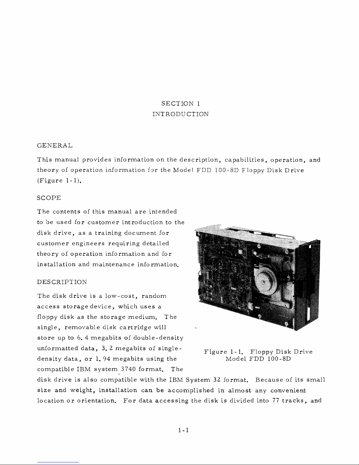
SECTION 1
INTRODUCTION
GENERAL
This manual provides information on the de
theory of operation information for the Mod
(Figure 1-1).
SCOPE
The contents of this manual are intended
to be used for custom er introduction to the
disk drive, as a training document for
cu stomer engineers requiring detailed
theory of operation information and for
installation and maintenance information.
DESCRIPTION
The disk drive is a low-cost, random
access storage device, which uses a
floppy disk as the storage medium. The
single, removable disk cartridge will
store up to 6. 4 megabits of double-density
unformatted data, 3. 2 m egabits of single-
density data, or 1. 94 m egabits using the
compatible IBM sy stem 3740 format. The
disk drive is also compatible with the IBM
size and w’eight, installation can be accoi
location o r orientation. F or data accessin
cription, capabilities, operation, and
1 FDD 100-8D Floppy Disk Drive
Figure 1-1. Floppy Disk Drive
Model FDD 100-8D
System 32 format. Because of its small
nplished in almost any convenient
I
the disk is divided into 77 tracks, and
1-1
Page 12

each track can be subdivided into as man y as 32 sec tors. A stepper motor positions
the read/write head at the track to be accessed . Index and sector holes punched into
the disk are sensed photoelectrically to produce sec tor and index pulses that permit
accessing the individual sectors of a track. When the optional write-protect slot in
the protective envelope is uncovered the w rite-pro tected condition is sensed photo
electrica lly, and write operations are inhibited.
Up to eight d rives can be interfaced to a single host controller. The controller
controls disk drive selection, head loading, track addressing, and read/write data
transfers.
When a disk cartridge is inserted and the acce s s door is closed, the drive spindle
rotates the disk at 360 revolutions per minute. When se lected, the drive accepts
a head load command, causing the read/write head to be loaded to the disk. With
the drive selected, sector/in d ex puls es, write-p r otect sta tus, track 00 position
status, and a read/write ready status is supplied to the controller. At the desired
track, a data tran sfer operation is performed; read-to the con trolle r, write-from
the contr o lle r, depending on the state of the write command.
During a write operation (disk not write-protected ), write data is input to the write
circuits. Fo r each write data pulse receiv ed , a flux reversal is recorded on the
disk by the read/write head.
During a read operation, each recorded flux rev e rsal is sensed by the read/write
head, converted to a raw data pulse and supplied to the controller.
Applications for the Floppy Disk D rive include:
• Key Entry System s
• Poin t-of-S ale Recording System s
• Word P ro cessin g System s
• Batch Termin al Data Storage
• Small Business Sy stem s Data Storage
• M icro p rogram Loading and E r ro r Logging
• Minicomputer Programs and Auxiliary Data Storage
1-2
Page 13
The drive provides random accessing of data with greater performance and
reliab ility and is an excellent alternate product to paper tape, reel-to - reel tapes,
card equipment, ca s settes, and cartridge drives.
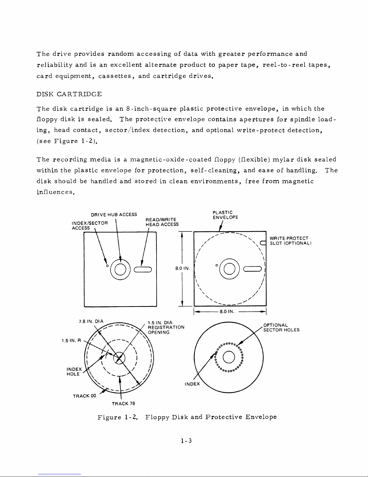
DISK CARTRIDGE
The disk cartridge is an 8 -inch -sq uare plastic protective envelope, in which the
floppy disk is sealed. The protective envelope contains apertures for spindle load
ing, head contact, secto r/index detection, and optional write-p rotect detection,
(see Figure 1 -2).
The recording m edia is a m agnetic-oxid e-coated floppy (flexible) m ylar disk sealed
within the plastic envelope for protection, self-cleaning, and ease of handling. The
disk should be handled and stored in clean environmen ts, free from magnetic
influences.
Figure 1-2. Floppy D isk and P rote ctive Envelope
1-3
Page 14
At no tim e should the surface of the med ia be touched, or the surface of the
envelope be written on. When not in use, the disk cartridge should be returned
to its protective storage envelope.
For reliable op eration, floppy disks should be stabilized in the same environment
as the using disk dr ives, for a period of at le a st five m in u tes, prior to installation.
The recommended floppy disk m eets the requirem ents of the following documents:
X3138/77-118 Am erican National Standard for Single Sided
Unformatted Flexible Disk Cartridge.
GA21-9190 IBM One-Sided, Original Equipment Manufacturing
Information.
EC M A/TC 1 9/? 7 / l6 Data Interchange on 200 m m Disk Cartridges using
double frequency recording at 13,262 ftprad on one
side.
Floppy disk ch a racteristic s are listed in Table 1-1.
Table 1-1. Floppy Disk Cha racteristics
Function
Characteristics
Disk Type
ANSI Standard
Disk Diam eter
7. 88 inches
Disk Thickness
0. 003 inch
Rotational Speed
3 60 rpm
Rotational Period
166. 67 ms
Ave rage Latency
83. 33 ms
Tracks
77
Track Density
48 tpi
Bit Density
3268 bpi (single density)
6536 bpi (double density)
Note: For m inim um runout the floppy disk should be loaded while the spindle is
turning.
1-4
Page 15
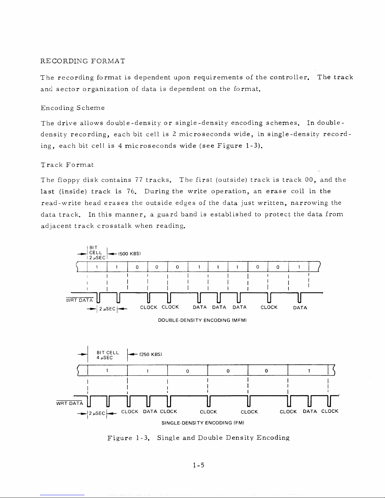
RECORDING FORMAT
The recording fo rmat l s dependent upon req u irem ents of the controller. The track
and s e ctor organization of data Is dependent on the format.
Encoding S chem e
The drive allows double-densIty or s Ingle-dens Ity encoding schemes. In double-
density reco rdin g, each bit cell Is 2 m icrosec o n d s wide, In s ingle-dens Ity rec ord
ing, each bit cell Is 4 mic roseconds wide (see Figure 1-3).
Track Fo r m a t
The floppy disk contains 77 tracks. The first (outside) tra c k is track 00, and the
last (Inside) track Ls 76. During the write operation, an era s e coll in the
re a d -w rlte head era se s the outside edges of the data just w ritten, narrowing the
data track. In this m anner, a guard band Is established to protect the data fro m
adjacent tra c k crosstalk when reading.
WRT DA TA
WRT DA TA
-► 1 CELL
12 mSEC
-* - (5 0 '0 KBS)
1
1
0
0 I 0
1
1 1
I I
I I
I I
FT
- ► ] 2 mSEC f— -
BIT C ELL
-
4 iuSEC
1
I
i n n n n r
j2 mSEC h - CLO CK D A TA C LO CK CLOCK CLO CK
j u i m j u if
CLOCK CLOCK DA TA D ATA DATA
DO U BLE -D E NSITY EN COD IN G (MF M)
(250 KBS)
1
0
i i ! i i
0
¥ u n n r
SING LE- DENS ITY E NCOD IN G (FM )
0
0
CLOCK DA TA
0 1
CLO CK D ATA CLOCK
1
Figure 1-3. Single and Double Density Encoding
1-5
Page 16
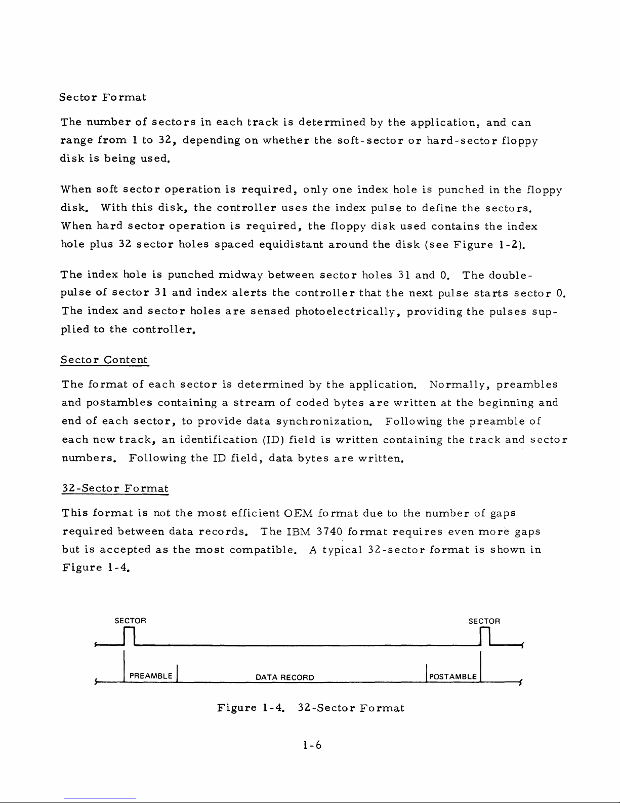
Sector Form at
The number of sectors In each track Is determined by the application, and can
range from 1 to 32, depending on whether the soft-se c to r or h a rd-se c tor floppy
disk is being used.
When soft secto r operation is required, only one index hole is punched in the floppy
disk. With this disk, the controller uses the index pulse to define the sectors.
When hard secto r operation is required, the floppy disk used contains the index
hole plus 32 secto r holes spaced equidistant around the disk (se e Figur e 1-2).
The index hole is punched midway between sector holes 31 and 0. The double-
pulse of sector 31 and index ale rts the controller that the next pulse starts sector 0.
The index and sector holes are se nsed ph otoelectr ically, providing the pulses sup
plied to the controller.
Sector Content
The format of each secto r is determined by the application. Norm ally, preambles
and postam b les containing a stream of coded bytes are written at the beginning and
end of each se c tor, to provide data synchronization. Following the preamble of
each new track , an identification (ID) field is written containing the track and sector
numbers. Following the ID field, data bytes are written.
32-Sector F orm at
This format is not the m o s t efficient OEM format due to the number of gaps
required betw een data records. The IBM 3740 form at requires even m o re gaps
but is accepted as the m ost compatible. A typical 32-s e c to r format is shown in
Figure 1-4.
SECTOR
SECTOR
PREAM BLE
DA TA REC ORD
POSTAM BL E
Figure 1-4. 32-S ector Form at
1-6
Page 17
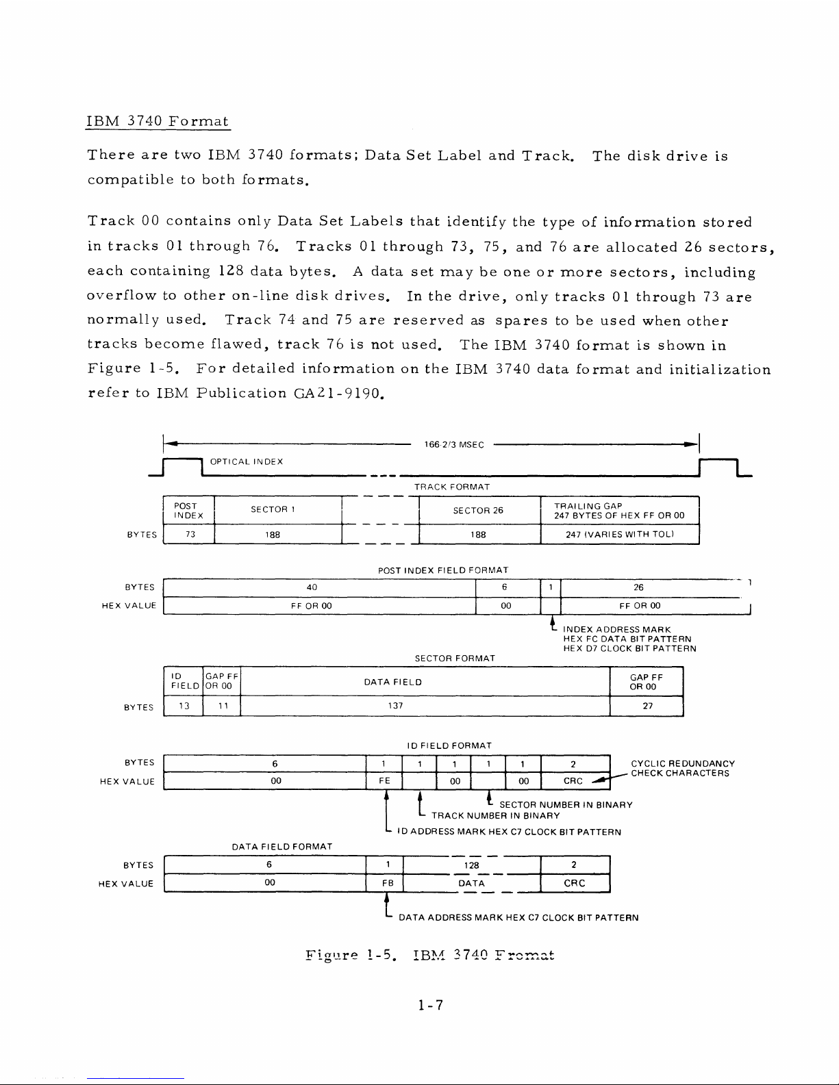
IBM 3 740 F o rm a t
There are two IBM 3740 form ats; Data Set Label and Track. The disk drive is
compatible to both form ats.
Track 00 contains only Data Set Labels that identify the type of information stored
in tracks 01 through 7 6. T r a cks 01 through 73, 75, and 76 are allocated 26 sectors ,
each containing 128 data bytes. A data set may be one or m o r e s e c tors, including
overflow to other on-line disk drives. In the drive, only tracks 01 through 73 are
no rm a lly used. T rack 74 and 75 are reserved as sp a res to be used when other
trac ks become flawed, track 76 is not used. The IBM 3740 form a t is shown in
Fig ure 1-5. For detailed information on the IBM 3740 data form at and initialization
re fe r to IBM Publication GA21-9190.
166-2/3 MSEC
J— L
OPTICAL INDEX
TRACK FORMAT
BYTES
J— L
POST
INDEX
SECTOR 1
SECTOR 26
TRA ILI NG GAP
247 BYTES OF HEX FF OR 00
73
188 188
247 (VARIES WITH TOL)
POST IND EX F IELD FO RMAT
BYTES
40 6
1
26
!
HEX VALUE
FF OR 00
00 FF OR 00 j
INDEX ADDRESS MARK
HEX FC DATA BIT PATTERN
HEX D7 CLOCK BIT PATTERN
BYTES
ID
FIELD
GAP FF
OR 00
DATA FIELD
GAP FF
OR 00
13
1 1
137
27
BYTES
HEX VALUE
BYTES
HEX VALUE
DATA FIELD FO RMAT
ID F IELD FO RMAT
6
1
1
1
1
1
2
00
FE
00 00 CRC
CYCLIC REDUNDANCY
CHECK CHARACTERS
t
L SECTOR NUMBER IN BINA RY
TRAC K NUMBER IN BIN ARY
L ID ADDRESS MAR K HEX C7 CLOCK BIT PATTERN
6
1
128
2
00
FB
DATA
CRC
I
DATA ADDRESS MA RK HEX C7 CLOCK BIT PATTERN
Figure 1-5. IBM 3 740 Frc
1-7
Page 18
DISK DRIVE ASSEMBLY
The disk drive ass e m bly can be installed in a standard 19-inch RETMA rack; two
horizontally, or four vertically. The drive can also be mounted in a table-top for
top loading applications.
The disk drive com p rises three m ajor assem blies-
• Printed Circuit Board (Electronics)
• Main Deck A ssem b ly
• Carrie r Assem b ly
Printed Circuit Board
All electronic circuitry required to convert the digital data input and output to
and from analog data for the rea d /w r ite head and head positioning information is
contained on one circuit board. Interface and DC connectors can be provided.
Logic is TTL with sele cted d iscrete and IC Components. The electron ics perform
the following functions:
• Read Chain
• Write Chain
• Ready Generation
• Index Detection
• Stepper M otor Control
• Interface D r ivers and Receiver s
• W rite-Protect (Option)
• Index/S ector Separator (Option)
• FM Data Separator (Option)
• Binary Select (Option)
1-8
Page 19

Main Deck Assem bly
The m ain deck a ssembly is the principal supporting asse m bly and contains the
following subassemblies;
Drive System
Positioning Svstem
Read Write S vs tern
Disk Cartridge Guide
and Ejector
Optical Sensing
- Spindle Drive m o tor, drive belt and pulley to
rotate spindle at 360 rpm.
- Stepping m o tor, lead s c rew and carriage, head
pressu re a rm and pressure pad to accurately
drive and position the read write head to the
desired track.
- Single-gap magnetic recording head with tunnel -
er a s e or s t raddl e - e rase feature. Read/w rite
head is contact type.
- Provides positive positioning and locking of disk
cartridge allowing prop er placement of the disk
cone. S pring-loaded ejection provides fast,
positive disk cartrid g e removal.
- Index and write - protect sensing by independent
LED and phototransistor sensing circuits. Also
track 00 sensing.
C a rrie r Assem bly
The c ar r i e r a s sem b ly is a secondary frame which pivots fro m the main deck
as sem bly and includes the following sub assem blies;
• Disk Centering Cone - P r e c isely cen ters and grips the floppy disk to the
s pindle.
• Head Load Mechanism - Solenoid, head p r e s s ure arm and pad. Ex erts
and sustains force, by the spring-loaded p r e ssu re
pad, to constrain the disk c artridge to the platten
and the read, write head.
Access Handle. Pushbutton latch release m echanism . Also
releases spring-loaded lock to discharge disk
cartridge.
OPTIONS-F E ATURES
The Floppy Disk Drive m ay be or d ered with basic configuration operating capa
bilities, or m ay be ord ered to include any or all available options. Each option
1-9
Page 20

offers unique operating features. Severa l options have connections designed into
the main printed circuit board, for low - c o s t custom er enhancement.
W r ite-P ro tect
The write-p rotect feature provides a write-inhibit function when a write -protect
floppy disk cartridge is used. The stored data is protected only if the cartridge
write-prote ct slot is present. With the slot cov ered, all write functions are
enabled.
Binary Select
The Binary Select option perm its any one of up to eight disk drives to be selected.
With the option installe d, SELECT lines are not dedicated but are used to contain a
binary select code. The SELECT 0 line is used to enab le/d isab le unit se lection,
while the SELECT 1, SELECT 2, and SELECT 3 lines contain a binary code between
0 and 7. When the SELECT 0 line is low (true), a decoder in the Binary Select
option log ic decodes the select code from the controller.
Radial Select
In the b a sic configuration, the disk drive does not accept com mands from the
contr oller, and does not supply status signals to the controller, until selected.
The purpose of this option is to allow commands to be accepted and status signals
to be supplied, each over separate lin e s, without the drive selected. The following
signals can be optionally configured for radial operation:
• S T E P and STEP IN (Step Command)
HDLD (Head Load Command)
• READY (Ready Status)
• INDEX and SECTOR (Index and Sector Pulses)
When dedicated lines are provided for these sig n a ls, the disk drive need not be
selected by the controller. Each line m u st be assigned a separate pin number on
the interface connector. Spare pins are provided for this purpose.
1-10
Page 21
The unit is modified for Radial Select operation by changing jumpers between the
existing etch pads. The etch pads are located on the main printed circuit board.
Hard S ector
In the b a sic configuration, the use of a hard sector disk causes the INDEX line to
produce one index pulse and 32 sector pulses per each disk revolution.
With the Hard Sector option installed, the index and sector pulses are separated
and supplied to the controller on independent INDEX and SECTOR lines.
16/8 Sector
When the Hard Sector option is installed, the addition of the 16/8 Sector option
provides a 2-bit binary counter that counts down the 32 sector pulses from a hard-
sector disk. This countdown perm its each track to be divided into 16 or 8 sectors,
instead of 32 sec tors. The output of the first stage (16 se c to r s ), or the second
stage (8 sectors) is connected to the SECTOR output line to the controller.
Auto Erase
The era s e turn-on and turn-off delays are internally controlled by the Erase logic.
When the controller activates WRITE, the leading edge of WRITE initiates a
200 -m icrose cond era se turn-on delay; the trailing edge of WRITE initiates a
530-m ic rosecond erase turn-off delay. If the straddle-e ra se configuration is used,
a str a ddle-e r a s e head m ust be installed. This option re m ov es the time delays.
Pads are provided for installation of this option.
Data Separator (FM only)
In the basic configuration, the RAW DATA line to the controller produces a pulse
for each flux reversal read from the disk. Consequently, the RAW DATA input
contains both clock and data pulses. F or this reason, the con troller must have
circu its that separate the clock and data pulses.
The Data Separator option is installed for the disk drive to operate in the sin gle
density encoding mode (FM) only. When installed, this option separates the data
and clock pulses input o ver the RAW DATA line. Data pulses are supplied to the
1-11
Page 22
controller o ver an FM SEP DATA line, and synchronized clock pulses over an
FM SEP CLK line. Proper operation of the Data Separator option is based on a
format with no m issing clock pulses.
Auto Head Load
In the basic configuration, the re ad/write head Is automatically loaded when the
unit is sele c ted, and is automatically unloaded when the unit Is deselected. Alterna
tively, the unit m a y be configured to load the head in resp onse to a HDLD command
from the controller.
Activity Indicator
In the basic configuration, the activity Indicator is on when the drive Is selected.
The Activity Indicator option provides a m eans of substituting for the SELECT
status sig nal, one of the following status signals:
• HEAD LOAD
• RDY
Etch pads are provided on the m ain printed circuit board to optionally OR either
of the above signals with IN USE.
PCB A ss e m b ly Option Configurations
The m ain printed circuit board can be supplied in a b asic configuration or with the
optional configuration including Hard Sector and Data Separator.
SPECIFICATIONS
A com prehensive list of principal specifications are provided in Table 1-2. The
list defines both sin gle-d en sity and d ouble-density c h ara cteristics, both disk drive
and interface logic le ve ls , and all physical and electrical par am eters.
1-12
Page 23
Table 1-2. Principal Specifications
Function
Characte ristics
Single -Density
Double - Dens ity
Disk Type
A NSI Standard
ANSI Standard
Storage Capacity
(Unfo rmatted)
Pe r Disk
Pe r Track
3. 2 megabits
41.7 kilobits
6. 4 megabits
83. 4 kilobits
T racks
77
77 <r.c
Tra ck Dens ity
48 Tracks P e r Inch
48 T rack s P e r Inch
Recording Density
Tra ck 00 (Outside)
Track 76 (Inside)
1836 bpi
(3672 fci)
3 2 68 bpi
(6536 fc i)
3672 bpi
(3672 fci)
6536 bpi
(6536 fci)
Recording Method
FM
MFM
Rotational Speed 3 60 rpm ±2.
5%
3 60 rpm ±2. 5%
\ y>r-r
:1 '
83. 33 milliseconds
175. 6 milliseconds
Rotational Latency
Average
Maximum
83. 33 milliseconds
175. 6 milliseconds
Single - Density
Double -Density
Acce ss Time
Track -to -Track
Tra ck 0 - Track 76
38 - Track Move
Settling Time
Head Load Time
3-8 milliseconds
456 milliseconds
226 m illiseconds
14 milliseconds
I'-f-f'
S ^ 5 r
,";.p m..s
25 milliseconds
3-8 m illiseconds
456 milliseconds
226 milliseconds
14 m illiseconds
25 milliseconds
Data Tran sfer Rate 250 kilobits/sec
500 killobits/sec
Era s e/W rite Recovery
Time
Tunnel -E ra s e
Straddle-E r a s e -<
.
580 m icrose conds
50 m icro s econds
(req'd for read to
stabilize after write
___
.
i
_ .1
\
Luiapi cicu
)
580 m icrosecond s
50 microseco nds
(req'd for read to
stabilize after write
COixiplelcu)
1-13
Page 24
Table 1-2. Principal Specifications (Continued)
Function
Characte r is tic s
Read /W rite Head
Single gap with s tra d d le - e r a se
Rea d /W rite -to- E ra se
0, 035 inch
Gap Spacing
Track Width
0. 0 13 inch
E r a se Width
0. 006 inch (on either side of track)
Spacing Between T racks
0. 02083 inch
Tra c k Centerline Radius
2. 029 + ,Q , where N - track num ber
4 o
/ n
n L \
yu-(V)
Logic Levels
Disk Drive
Logical 1 (True) = +2. 5V to + 5. 5V
Logical 0 (False) = 0. 0V to + 0. 4V
Interface
Logical 1 (True) = 0. 0V to + 0. 4V
Logical 0 (False) = +2. 5V to + 5. 5V
AC Input P ow e r
Standa rd
115V (90- 127V) 60 Hz ± 0. 5 Hz
115V (90- 127V) 50 Hz ± 0. 5 Hz
Optional
230V (180-253V) 60 Hz ± 0. 5 Hz
230V (180 - 25 3V) 50 Hz ± 0. 5 Hz
Voltage Dropout 100%, 10 milliseconds once each 600 seconds
Motor C u rrent (Max)
|
Start
1. 0 am p e re for 120 volts AC
0. 6 am peres for 220 volts AC
Run
0. 5 am peres for 120 volts AC j
0. 3 am peres for 220 volts AC
DC Input Power
+ 24 volts ± 5%, 1. 8 am peres maximu m
+ 5 volts ± 5%, 1. 3 am p e r e s m ax i m um
Reliability
M T B F
6000 hours (after initial 200 hours)
MT T R
Less than 20 minutes
1-14
Page 25
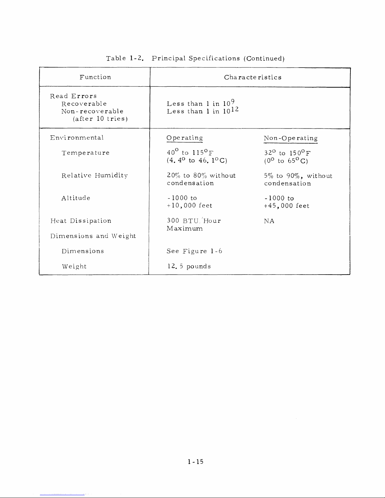
Table 1-2. Principal Specifications (Continued)
Function
Characte r is tics
Read E rro rs
Recoverable
Non-reco v e rable
(after 10 tri e s )
Less than 1 in 10^
Less than 1 in 1 0 ^
Envi ronmental O pe rating
Non-Ope rating
Tem p e rature
40° to 115°F
(4. 4° to 46. 1°C)
32° to 150°F
(0° to 65°C)
Relative Humidity
20% to 80% without
condensation
5% to 90%, without
condensation
Altitude - 10 00 to
+10,000 feet
- 1000 to
+4 5,000 feet
Heat Dissipation
Dimensions and Weight
300 BT U /Hour
Maxim um
NA
Dimensions See Figure 1-6
Weight
1 2. 5 pounds
1-15
Page 26
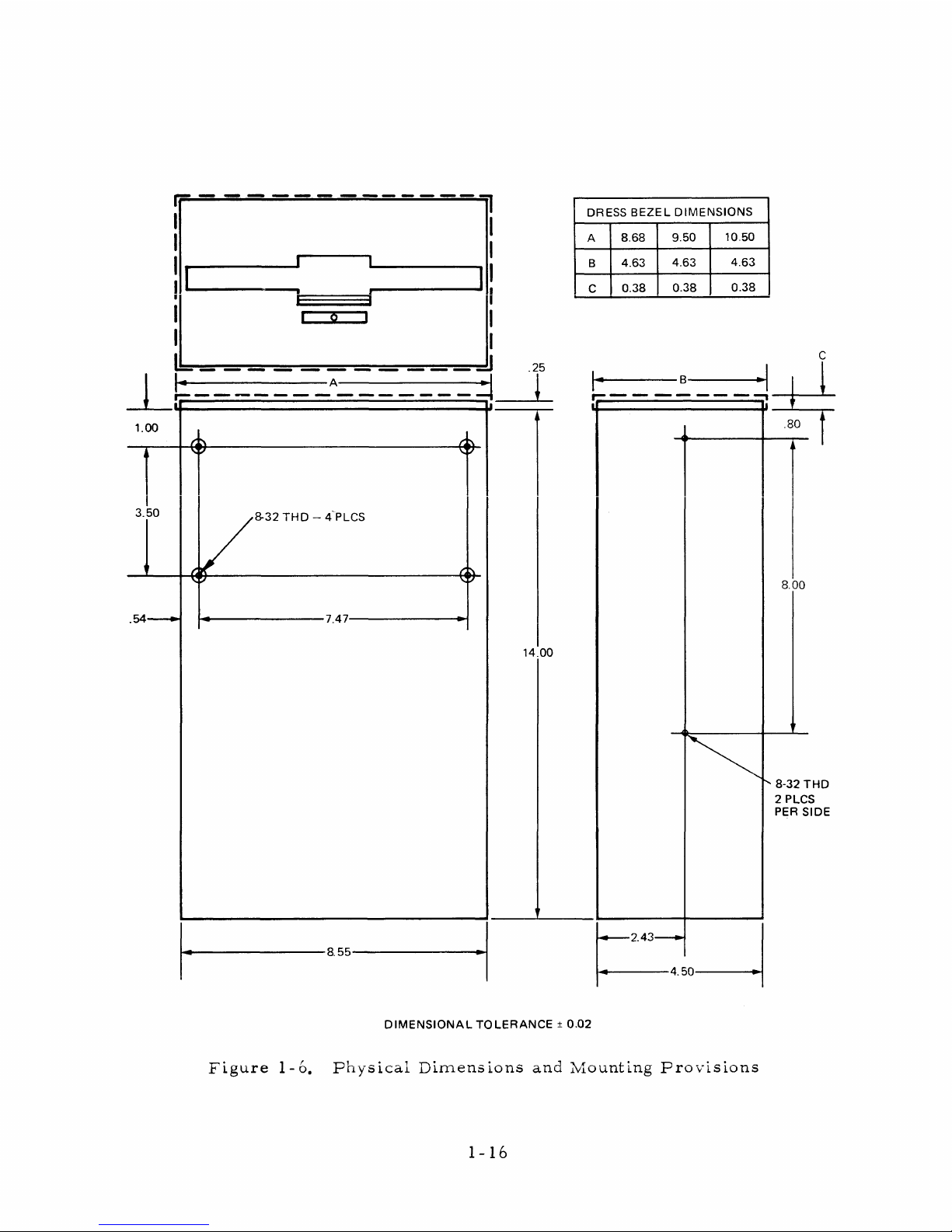
1.00
3.5 0
.54-
8-32 T H D — 4 PLCS
■7.47-
-8.5 5-
&
14.00
DRESS BEZEL DIM E N SIO N S
A
8.68
9.5 0
10.50
B
4.6 3
4.6 3
4.6 3
C
0.3 8
0.3 8
0.3 8
8-3 2 T H D
2 PLCS
PER SIDE
DIM ENSIO NAL T O L E R A N CE ± 0.02
Figure 1-6. Physical Dimensions and Mounting Provisions
1-16
Page 27

SECTION 2
OPERATION
GENERAL
The Floppy Disk Drive opera tes under complete control of the host controller,
after a floppy disk has been manually inserted. A front panel indicator is p ro
vided to indicate operating status.
DAILY OPERATION
The operating environment and the op e ra to r's careful handling of the disk drive
and the floppy disks enhance the appearance, and greatly extend the operating life
of the equipment.
Floppy Disk, Ilandl ing and Storage
The floppy disk is the data storage medium. The disk is sealed in a protective
envelope, in which are access holes for the read/writ e head, index and s ecto r
holes, disk centering hole, and optional write-p rotect slot (see Figure 2-1).
For external e r r or - f re e operation of the disk drive, the following disk handling
practic es a re recom m ended:
• P rior to use, place in same operating environm ent as disk drive, for at
least 5 minutes
• Never - place heavy objects on envelope
- write on protective envelope, only on label
- touch disk surface while handling
- attempt to clean disk surface
• Always - return floppy disk to storage envelope when not in use.
2-1
Page 28
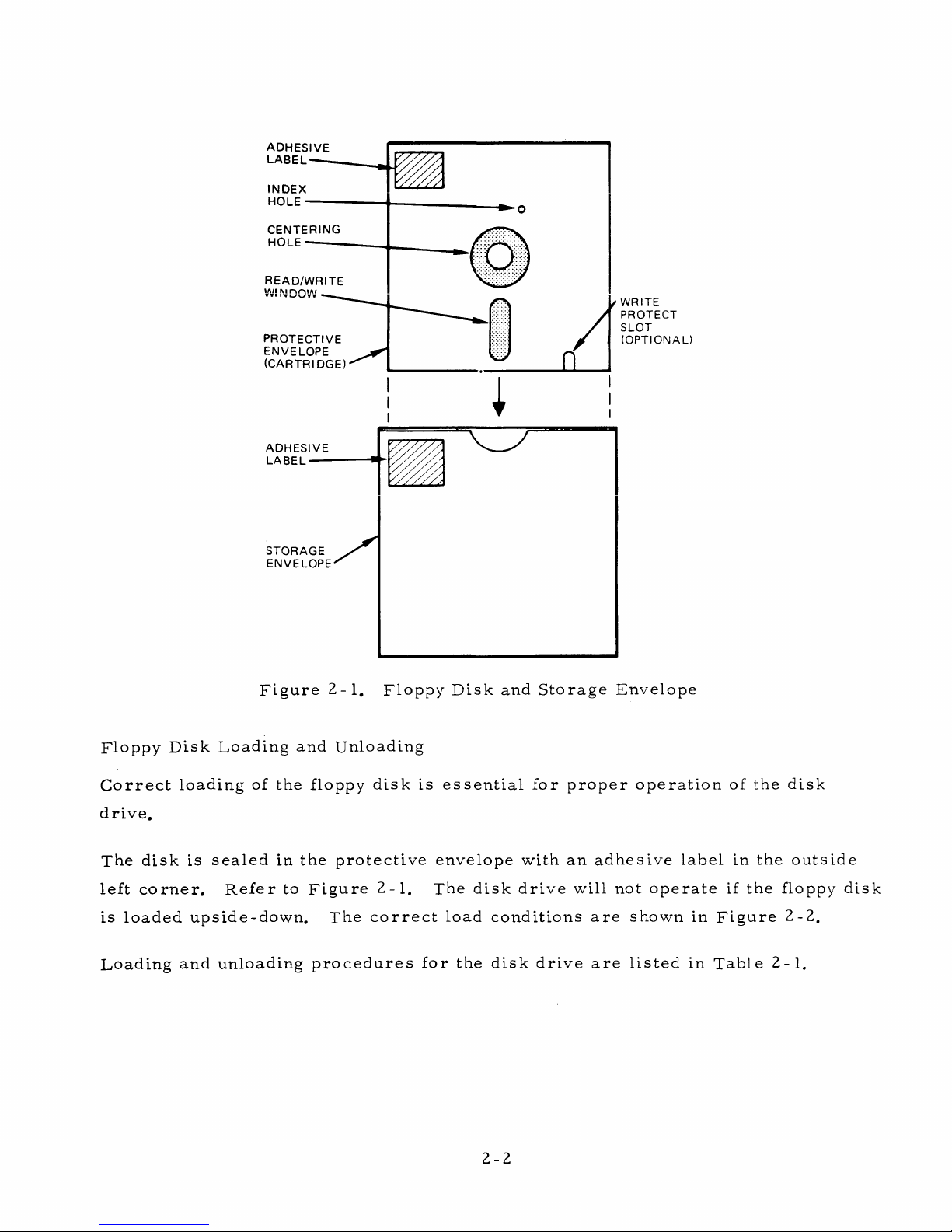
Figure 2-1. Floppy Disk and Storage Envelope
Floppy Disk Loading and Unloading
Correct loading of the floppy disk is essential for pro p er operation of the disk
drive.
The disk is sealed in the protective envelope with an adhesive label in the outside
left corner. Refer to Figure 2-1. The disk drive will not o perate if the floppy disk
is loaded upside-down. The c o rrect load conditions a re shown in F igure 2-2.
Loading and unloading procedur es for the disk drive are listed in Table 2-1.
2-2
Page 29

Figure 2-2. Floppy Disk Loading
Table 2-1. Floppy Disk Loading and Unloading
A ction
i
Reaction
P r e ss front panel
pus hbutton
Front panel unlatches and raises to open
position. Spindle cone removed fro m
drive cone. Disk cartridge released from
spring-loaded latched condition.
Insert floppy disk, label
up, into slot fully until
stopped
Disk cartridge co rrectly positioned over
drive spindle and firmly latched in spring-
loaded condition
Lower front panel until
latched
Spindle cone lowers and ce nters disk with
firm pre s s u r e. Disk rotates no rmally
with interlock closed.
W rite -P ro tect
W rite- p rotect guards against the destruction of stored data by circuit malfunctions
or during test and operations. A read and write disk cartridg e will have no open
slot punched in the c a rtridge, or the slot will be covered with an adhesive opaque
tab. A read-only disk c artrid g e will have an open punched slot ready for light
sensing by the write-p rotect circuit.
2-3
Page 30

SECTION 3
THEORY OF OPERATION
GENERAL
This section contains descriptive information on each function of the disk drive and
detailed theory of operation. The information is intended to serve as a training
guide for technical personnel requiring in-depth knowledge of the disk drive.
The disk drive contains three major s y s tem s, as shown in Figure 3-1:
• Control System
• Positioning System
• Read /W rite System
Figure 3-1. Floppy Disk D r ive, Simplified Block Diagram
3-1
Page 31

CONTROL SYSTEM
The control system provides the interface circuitry between the disk controller and
the disk drive. The operational status Is m onitored and reported to the disk con
troller. The disk controller add r e s ses a disk drive for on -line operation by ac t i
vating a unique s e lect line. Commands are then received and executed by the
selected disk drive. This technique allows m ultiple disk drive units to share co m
mon interface lines, while remaining individually selectable.
Command Execution
Commands are received by the disk drive in the form of a low -level interface
signal which designates one of the following operations:
•
SELECT
Place s disk drive on-line with controller
w
CTt?n
O X llj JT
Enables re a d /w rite head positioning
•
ST E P IN Determines read/w rite head direction
•
HEAD LOAD
Place s disk recording surface in contact with
(HDLD)
read/write head
•
WRITE
Enables write current to turn on and Inhibits
(WRT)
read output
•
WRITE DATA
Enables write data transfer from controller to
(WRT DATA) disk drive
SELECT and HDLD commands m ust precede a read or write operation. SELECT
enables all Input/output gates, while HDLD positions the read/write head for w r it
ing or reading on the floppy disk.
ST E P m oves the read/w r ite head to either a higher or lower track position depend
ing on the STEP IN line. Since relative track positioning is used, the disk con
troller m aintains current track position and generates the number of pulses ne ce s
sary to achieve a new track position. Once positioned, the disk controller initiates
a read or w rite operation
In a Write operation, the disk drive records the data in the sam e encoding method
presented by the disk controller.
3-2
Page 32

Status Sensing
Five disk drive status signals are gated to the i/O lines when the disk controller
selects a disk drive.
• WRITE PRO T E C T Hardw a re w rite -protect condition exists (if
(WRT PROTECT) write-protect disk used)
• TRACK 00
Read/write head positioned at track 00
• INDEX
Start of each tra ck
• SEC TOR
Start of new secto r (if sectored disk used)
• READY
Signifies disk drive is operational
• DISK CHANGE
Signals that the pack may have been changed
READY, WRT PR O TEC T , and DISK CHANGE a re static level status signals.
Ready status indicates a floppy disk is loaded and up to operating speed. Write-
protect status indicates write data cannot be recorded on the disk. Disk change
status indicates the door was opened during drive manual action. Index status
oc curs once per disk revolution. Track 00 status is available for initializing the
disk con troller trac k addres s register. This signal is developed from a photo
tr a n si s to r when the carria g e is m echanically aligned with track 00, and the stepper
motor is at phase A.
by moving the read/w rite head one track position per pulse. The following functions
accomplish this operation.
• Stepper Motor Control
• Stepper Motor
• Carria g e A ssembly
Stepper Motor Control
The step m otor control converts serial S T EP pulses to three sequential control
signals. Each signal energizes one of the stepper motor windings, causing a
15-degree rotation of the moto r shaft (one track position).
POSITIONING SYSTEM
The positioning system responds to STEP pulses received fro m the disk controller
3-3
Page 33

Stepper Motor
The v a riable-re lucta n c e stepping motor provides precision positioning of the rea d /
write head. The stepper m otor is energized by + 24 volts dc and operates in either
Detent or P ositioning mode.
In the Detent m ode, an internal generated m a gnetic field holds the rotor in a
fixed position. To m ove from detent, one of three control lines is grounded, d riv
ing the rotor to the next detent. Sequentially grounding control windings causes
the rotor shaft to rotate through detent positions at a maxim u m rate of 333 steps
per second. A lead screw on the exposed rotor shaft converts rotary movements
to linear movement to drive the carria ge assembly.
Carriage Assem bly
The carriage asse m bly rides on a lead screw while a fixed way prevents the
carriage from skewing. The way serve s as a guide while the lead screw drive
performs the in and out positioning.
The read/write head, attached to the carr iage asse m b ly , contacts the recording
surface when the drive is selected. This command re l e a ses a spring-loaded head
load arm that m ove s the floppy disk into contact with the read/w rite head.
READ/W RITE SYSTEM
The rea d /w r ite system records encoded data during a Write operation, and
retrieves data during a Read operation. The write (WRT) signal from the c o n
troller designates a Read when high or a Write when low.
Read/W rite Operation
The read/write head is esse n tia lly an electromagn et that can concentrate a high
magnetizing force over a very sm all area of the adjacent recording surface. When
recording, the flux field is alternated to magnetize the disk with the desired bit
pattern. The read/w rite head also contains a tunnel-erase or stradd le-erase
electromagnet, the function of which is to e ra se the edges of the recorded track as
data is being written. The width of the track is narrowed to approximately
0. 013-inch by this technique, to m inimize the effect of data previously written on
the track and possible crosstalk between tracks.
3-4
Page 34

When reading, the read/w rite electromagn et o perates as a sensor. A flux r eversal
on the recorded track induces a voltage a c ro s s the electromagnet coils. This vo lt
age is amplified and conditioned to recover the recorded information.
FUNCTIONAL DESCRIPTION
The disk drive is a m as s m em or y device featuring a removable floppy disk and
contact recording. The 250 khz/bit t ran s fer rate provides a high speed transfer
of data between the disk drive and a host disk controller. Multiple disk drives may
be connected in a radial or daisy-chained configuration with individual selection
and status monitoring.
The disk drive requires o p erato r intervention only for loading and unloading the
floppy disk; after which the disk controller rem otely operates the unit. Input ac
and dc power, control signals and write data a re supplied by the controller; the
disk drive responds with operating status and read data. A detailed functional
block d iagra m is shown in Figure 3-2.
WHITE PROTECT LED
Figure 3-2. Detailed Functional Rlnrk Diaa ram
O
...........
3-5
Page 35

The disk drive c o m pris e s the following functional systems;
• Spindle Drive System
• Spindle System
• Read Write Head Positioning System
• Head Load System
Spindle Drive System
The spindle drive sy stem provides rotational mo vemen t of the spindle using a
single-pha se moto r selected to m atch p rim ar y power of the host system. Various
drive m o tors are available that a ccomm o d ate prim ary power require m ents of 115
and 230 volts ac at 50 or 60 Hertz.
Rotation of the spindle is provided by a belt and pulley connected to the drive m otor
roto r shaft (see F ig u re 3-3). The d rive pulley is selectable for either 50 or 60 Hz
input power for rotational speed of 360 revolutions per minute. A floppy disk is
engaged with the spindle drive hub by the spindle syste m centering cone.
MO
PUI
SPINDLE AN D
PU LL E Y
Figure 3-3. Spindle Drive Sy stem
3-6
Page 36

Spindle System
The spindle sy stem consists of a spindle and a centering cone mounted on the deck
and c a r rie r, respectively. In the unload position, the centering cone ca rrie r is
pivoted open creating an aperture through which the floppy disk is inserted. In this
position, the centering cone is lifted, disengaging the disk from the spindle hub.
To load a disk, the o p e rato r in serts the
floppy disk then closes the handle, which
latches the c ar r ie r in the operating mode.
The centering cone (see Fig u re 3-4) is
attached to the c arrie r and is an open-
splined n on-m etallic device that p erfor m s
two functions:
• Aligns the disk media to the
spindle hub
• Engages the disk med ia to the
spindle drive system
As the ca r r ier is pivoted to the load po si
tion, the centering cone enters the floppy
disk center. Just pr ior to the fully closed
position of the handle, the centering cone
expander is automatically activated to
expand the centering cone, which grips and
aligns the floppy disk to the spindle, thus
centering the disk on the spindle.
Figure 3-4. Spindle System
Read/W rite Head Positioning System
The positioning sy stem co m pr ises a car riage asse m bly , a re a d /w r ite head and a
bidirectional stepper m o tor and lead screw (see Figur e 3-5). The stepper motor
rotational m ovements are converted to linear motion by driving the lead screw and
ca rriage assem bly .
3-7
Page 37

The re a d /w r ite head carriage rides on the
lead screw shaft and is held in horizontal
alignment. When the stepp er m oto r is
pulsed, the lead screw rotates clockwise
or counterclockwise, moving the carr ia g e
in or out, respectively.
The stepper m o tor has three pairs of
windings. In Detent, current flows in one
winding and maintain s the rotor in e l e ctro
magnetic detent. F o r positioning, the
windings are driven sequentially, causing
the rotor to rotate through detent positions
until the STE P c omm ands are halted. The
rotor then locks in that position, with the
last winding being driven. The sequence
in which the ste pper m o tor windings are
pulsed dictates rotational direction and,
subsequently, higher or low er track
ad dressing from the relative position.
Head Load S ystem
The head load syste m is, basically, a solenoid driver and a solenoid. When a c ti
vated by the HDLD com m a nd, the spring-loaded head load pad is released and
brings the recording su rface of the floppy disk into conform ance with the head.
To m inim ize disk surface and re a d /w rite head w ear, the HDLD com m and is
gated with SELECT . In the deselect or Idle m ode, head loading is automatically
disabled. The Head Load c om m and re quire s a 25-millisecond execution time.
Control and Data Timing
Figure 3-6 shows the sequence of control and data timing requirements.
Figure 3-5. Re ad/W rite Head
Positioning System
3-8
Page 38

AC POWER
_ J
-------
T
2 SEC MIN
DC POWER
90 ms MIN
V A LI D OUTPUT
CONTROL SIGNALS
SELECT
500 ns MAX
READY
"► HDLD
STEP IN
1 ms MIN
STEP
10 MS MIN
RAW DATA
WRITE
WRT
DATA
■25 ms MIN
■h }
I li
FORWARD
*
REVERSE |
t n T Hin j
jr*— 1 MS MIN
il
_L*J | , 3 ms MIN U
I | | 8 ms MAX I
1 I I
30 ms MIN
"tZZT
READ DATA I
200 ms ( TUNNEL ERASE)
0 ms (S TRADDLE ERASE).
ERASE h
1 BIT TIME M AX *
READ DATA
I I
50 ms MIN
V — !T
►J ■■■ »i U
530 ms (TU NN E L ER ASE)
0 ms (S T R ADD L E ERASE)
II
* 4 MICROSECONDS FM
2 MICROSECONDS MFM
8 MICROSECONDS FM
4 MICROSECONDS MFM
WRITE DATA
2 BIT **
TIMES MIN
Figure 3-6. Control and Data Timing
3-9
Page 39

LOGIC CONVENTIONS
The disk drive uses standard 5-volt TTL log ic, where a voltage m o r e positive than
+2. 4 volts (turn-on threshold) is considered a logica l one (high), and a voltage more
negative than +0. 4 volts (turn-off threshold) is con sidered a logical zero (low).
Interface signal logic le v e ls are inverted by line rece iver s and line dr ivers for use
by the disk drive and the contro ller, respectively. F o r all interface sign a ls, a
voltage m ore positive than +2. 4 volts (turn-off threshold) is considered a logical
zero, and a voltage m ore negative than +0. 4 volts (turn-on threshold) is considered
a logical one (see Figure 3-7).
The logic symbology used in the disk drive is shown in Figure 3-8. Each element
is describ ed and all conditions are defined.
DETAILED LOGIC DESCRIPTION
The detailed logic description is divided into three major functions:
• Control Logic
• Read/W rite Head Positioning Logic
• Read/W rite Logic
CONTROL LOGIC
The control logic contained in the disk drive perform s three prim e functions:
• Accepts controller SELECT command and enables all interface logic
• Detects and provides index and optional sector pulses
Figure 3-7. Interface Logic L evels
3-10
Page 40

GATES
HIGH IN, HIGH OUT
SCHM ITT A MP LIFI ERS
r > -
- D - J
HIGH IN, LOW OUT.
LOW IN, HIGH OUT
LINE D RI VER
HIGH IN, HIGH OUT.
OP ER AT ION AL
R = REFER ENCE VOLTAGE
OUTPU T VO LTAG E RANGE
DEPENDS ON REFERENCE
VOLTA GES A ND RAN GE OF
A A ND B INPUTS. A IS SEEN
AM PL IFI ED AT THE OUTPUT
B IS SEEN AM PL IFI ED AND
INV ER TE D A T THE OU TPUT
IF BOTH A AN D B AR E
ACT IVE, OUTPU T IS AN
ALG EB RA IC AD D ITIO N OF
INPUTS
AL L HIGHS IN, LOW OUT.
ANY LOW IN, HI GH O UT
EXCLU SIVE OR GATE
INPUTS NOT ID EN TI CA L,
HIGH O UTPUT INPUTS
IDE NT ICA L. LOW OUTPU T
1C ONE-SHOTS
OUTPUT PULSE DURAT ION
DET ER MIN ED BY E XT E R
NAL R C VA RIAB LE
RESISTOR IN DICATES
TIME A DJ UST ABL E OVER
A RA NGE
I F A GOES LOW. B GOES
HIGH FOR X TIME AND C
GOES LOW FOR X TIME.
CROSS-COUPLED LATCH
BO T H SET AN D R ESE T
HI G H, NO CHA N G E . SET
IN PU T LO W, Q IS HIG H
A N D Q IS L OW. RE SET
LOW , Q IS L OW AN D Q
IS HIG H . B OTH SET A N D
RES ET LOW, Q A N D Q
BO TH H IG H .
LIGH T E MIT TIN G DIODE
IF A IS MOR E POSITIVE
THA N B, L IGH T IS EM ITTED .
IF B IS MORE POSITIVE
THA N A, NO LIG HT IS
EMIT TED
D FLIP-FLOP
D HIGH AND C POSITIVE
TRA NS ITI ON = Q H IGH; D
LOW AN D C POSITIVE
TRA NS ITI ON = Q LOW.
EXCEPT: PR LOW HOLDS_Q
HIGH; CLR LOW HOLDS Q
HIGH. Q IS ALW A YS THE
INVERSE OF Q, EXCEPT
WHEN PR AN D CLR ARE
BOTH AT THE_SAME
TIME (Q A ND Q W ILL BOTH
BE HIGH)
JUMPERS
DAR K PADS
INDIC ATE JUMPERS
NO RM A LL Y FACT ORY
INS TA LL ED
LIGHT PADS
INDIC AT E OPTION AL
JUMPER IN ST A LL AT IO N
PHOTO TR ANS ISTO R
LIG HT ACTIVA TES
PHOTO TR ANS ISTO R
Figure 3-8. Logic Symbology (Sheet 1 of 2’
3- ii
Page 41

LOGIC LSI C HIP
THIS LOGIC CHIP IS A SEMI-CUSTOM LSI 22-PIN INTEGRATED CIRCUIT. THE CHIP USES C-MOS FET PAIRS AS
BUILDING BLOCKS FOR GENERA TING THE REQUIRED LOGIC FUNCTIONS. THE C-MOS REQUIRES LITTLE
CURRENT AND IS INSENSITIVE TO NOISE. A L L OUTPUTS WILL SINK 2.0 MILL1AMPERES. ALL INPUTS
REQUIRE 0.2 MILLIAMPER ES TO BE D RIVEN AN D THE INPUT AND OUTPUT SIGNALS AND PINS ARE
IDENTIFIED AS SHOWN AND AS LISTED BELOW.
PIN INPUTS
PIN OUTPUTS
+5V
1 LTRK 00
2 PHASE C
4
+5V 3
RDY
5
SELECT
6
STEP
7 LSTEP
9
DISK CHG
8
STEP INHIBIT
11
HDLD
10
STEP OPT
16
TRK 00
12 SEL OPT
20 PHASE A
13
LHDLD
22 PHASE B
14
DOOR CLOSED
15
POR
17 INDEX
18 GND
19
STEP IN
21 PHASE OPT
5
SELECT
1 7
INDEX RDY
3
STEP
DISK CHG
10
INHIBIT
20
STEP OPT
PHASE A
19
15
STEP IN
PHASE B
22
2
POR
PHASE C
12
SEL OPT
7
--------
IMI 4060 2
LSTEP
13
14
16
LHDLD
TRK 00
DOOR CLOSED
-
LTRK 00
STtP
------
21
PHASE OPT HDLD
11
18
INPUTS - THE DERIV ATION OF THE INPUTS IS EXPLAINED IN OTHER SECTIONS OF THIS MANUAL.
OUTPUTS - A BRIEF DESCRIPTION OF ALL OUTPUTS AND THEIR EQUATION IS LISTED BELOW.
HDLD = (LHD LD) (SEL OPT) (DOOR CLOSED)
READ/WRITE HEAD LOADED IF DRIVE IS SELECTED, IF A HEAD LOAD COMMAND IS
RECEIVED, AND PROVIDED THAT THE ACCESS DOOR IS CLOSED
TR K00 = (LTR K 00) (PHASE A)
TRACK 00 SIGNAL SENT TO CONTR OLLER IF OPTICAL SWITCH INDICATES TH AT CARRIAGE
BETWEEN TRACK 00 AND TRACK 1-1/2, AN D TH AT PHASE A OUTPUT IS PRESENT
STEP = (STEP OPT! (LSTEP! (STEP INHIBIT)
STEP OUTPUT ACTIVE IF STEP OPT AND LSTEP BOTH ACTIVE AND NOT DISABLED BY STEP
INHIBIT
RDY = (PORI (DOOR CLOSED) (TWO INDEX PULSES)
READY IS INACTIVE, HIGH, DURING POWER-ON AND IF DOOR IS OPEN
READY IS ACTIVE, LOW, IF POWER IS APPLIED WITH DOOR CLOSED, FOLLOWING TWO
INDEX PULSES AT INPUT
PHASE A = ACTIVE AT TRACK 00 WITH PHASE OPT HIGH. PHASE A AC TIVE EVERY THIRD TRACK
(0, 3, 6, ETC)
PHASE B = ACTIVE AT TRACKS 1, 4, 7, ETC
PHASE C = ACTIVE AT TRACKS 2, 5, 8, ETC
Figure 3-8. Logic Symbology (Sheet 2 of
Z\
3-12
Page 42

• M onitors flexible disk rotation to develop a ready status for the
Controller.
Select
When SELECT is inactive (high), the select logic inhibits all interface input
re c e ivers and output driv e r s to and from the disk drive. The select logic is
prim arily c om p rised of OR gate 4A, NOR gate 5A , and inverter 6B (see F ig
ure 3-9).
SE LE CT 0
SE LE CT 1
SELE CT 2
SELE CT 3
J3
26
28
30
32
r R A D I A L SEL I
I OPT IO N I ________
0 I SELE CT
1
0^ - 4
r s
BIN A R Y SELEC T O PTIO N
4-TO -IO
LINE
DECO DER
7C
0 -0 0
o-a
4
D-D 2
0 - D 6
0 -D 1
CHD 5
0 -D 3
0 - D 7
D - "
CH*
CH-
[ fn i
CH
4A
5A ^
-------
" 3 |6 B ^O
-----
f
n ~ - s n
i p HD I
SELECT
SELECT
-c>
4k >
( T O SEL O P TOF
LSI C IRC UIT 6D
/ TO LH D L D OF
LSI C IR C U IT 6D
Figure 3-9. Select Logic
When SELECT is inactive, gate 4A outputs a high through OPT D and is inverted
by 5A causing a low S ELECT signal to inhibit all disk change, ready, index, sector,
write - p r o tect, and track 00 logic. Inverter 6b outputs a high SELECT to inhibit
all head load, step, door interlock, and activity LED logic.
As shipped from the factory, a ju m p er plug is installed between the "0" Radial
Select pads, causing SELECT 0 to drive 4A. This assigns physical address 0 to
the disk drive. One of three other a d dre ss e s can be assigned, SELECT 1,
SELECT 2, o r SELECT 3, by rem oving the jum p er between the "0" pads and
installing it between the d esired Radial Select pads. Only one jum per can be con
nected to the disk drive. With the Radial Select feature, up to four disk drives
can be connected in daisv-chain fashion
3-13
Page 43

Binary Select (Option)
The Binary Select option allows up to eight disk drives to be da isy-ch ained to the
contro ller, with a d dresses 0 through 7. The option is comprised of 4 -to-10 line
decoder 7C, and eight sets of jumper pads (see Figure 3-9).
When SELECT 0 is inactive, the decoder is inhibited and all outputs are high.
When SELECT 0 is active , the decoder is enabled and only one low output is pro
duced. The decoder accepts a binary coded address on three selec t lin e s,
SELECT 1 through SELECT 3, and decodes them to produce a low output decimal
equivalent corresponding to the desired address.
The jumper plug is rem oved from the radial se lect option and installed between
the pads desired to assign the independent physical address of the disk drive.
Table 3-1 indicates the logic state of the SELECT lines for selecting each drive.
Table 3-1. Disk Drive Selection
Drive
SELECT 1
SELECT 2 SELECT 3
Selected
1
1 1
0
0
1 1
1
1
0
1
2
0 0
1
3
1
1
0
4
0
1
0
5
1
0
0
6
0
0
0
7
0 = Inactive state of interface signal (high)
1 = A ctive state of interface signal (low)
3-14
Page 44

Index/S ector Detection
A light-emitting diode (LED) and p hototra nsistor are physically positioned in the
disk drive to sense the index and secto r (optional) holes in the floppy disk. If the
Hard Sector option is installed, a 32 -sector disk should be used. Index pulse
detection logic is shown in Figure 3-10.
+5V
TO HAR D
SEC TOR
OP TION
FROM HA RD
SECTOR
OP TION
J l N D E X
□ HS
SELECT
ENAB LE
L
7B
J3
20
IN D E X
LT
TO R E A DY
LOGIC
Figure 3-10. Index Detection Logic
The index detection logic is com p rised of an LED and phototransis tor, a com pa r a
tor and an output line driver. The negative input to c o m para tor 3A is driven by the
output of the activated phototrans isto r. R e s isto r R32 supplies bias current to the
LED.
When the media blocks the LED output from the phototransistor, the input to the
co mparator is high. When the index hole is sensed , the input to the co m para tor is
low. Resi stors RIO, R9 and R l l provide a positive referen ce threshold voltage of
+ 2. 5 volts. F o r each index hole sensed, the com p arator output is a positive INDEX
pulse, nom inally 1. 7 millisecond in duration, and occ urring once per disk revolu
tion. The INDEX pulse is input to inte rfac e line d river 7B and inverted to provide
a low INDEX signal to the controller. F igure 3-11 shows index pulse timing.
Norm ally , OPT 0 is installed for soft se ctor operation.
Page 45

Hard Sector (Option)
With the Hard Sector option installed, and by
using a 3 2 -secto r floppy disk, the com para t o r
provides 32 SECTOR pu lse s, equally spaced
5. 2 m illiseco nds apart, during e ach disk
revolution, plus an INDEX pulse that oc curs
halfway between sector pulses 31 and 0.
Re fer to Fig u re 3-12.
The positive-going leading edge of the SEC TOR pulses from the c o m parator (F ig
ure 3-12) triggers one-shot 1C to produce a 0. 4 millisecond pulse, and complement.
The positive-going trailing edge of the complement (Q), trig g e rs one-shot 1C which
times for 3. 6 m illiseconds. After being triggere d by SECTOR pulse 31, the one-
shot is timing out* During this period, the INDEX pulse occ u r s , and one-shot 1C
can not be triggered.
The output of INDEX gate 2C drives INDEX gate 2C and resets flip-flop 3C of the
16 o r 8 Sector divider logic. The output of INDEX gate 2C is input to interface
166 .67 ± 3.3 3 MS ■
? 3-
■t
er
LJ
1.7 i 0.5 MS
Fig ure 3-11. Index Tlmins
INDEX line driv er 7B and the Ready logic. S ECTO R gate 2C provides the SECTOR
pulse inputs to interface SECTOR line driv e r 7B if the 32 - sector ju m pe r is installed.
The output of SECTOR gate 2C also drives the clock input to the 16 or 8 Sector
option, if it is Installed. Divlde-by-2 flip-flop 3C produces 8 and 16 SECTOR
pulses per disk revolution. If the 16-sector jum p er is installed, 16 pulses per
revolution are sent to the controller by interface SEC TOR driver 7B. If the 8 -sec
tor jum p e r is installed, 8 pulses per revolution will be provided to the controller.
Fig u re 3-13 shows INDEX and SEC TOR timing.
Ready
The Ready logic is used to m onitor the INDEX pulse for the rotational speed of the
floppy disk. When the required disk speed is reac h ed, the READY status is sent
to the controller. Once per revolution, the INDEX pulse is input to LSI chip 6D
(see Figure 3-14).
3-16
Page 46

F i g u re 3-12. H ard Se c to r and 16 o r 8 Sec to r Option L ogic
2.6 i 0.065 MS
F i g u re 3-13 . IN D E X /SE CT O R Tim in g
3-17
Page 47

+5V
F i g u r e 3-14. R ea d y Logic
When P OR is input and the a cc es s do or is clo sed , the LSI circ u it will p r o d u ce a
RDY signal af t e r re c e iv i n g two INDEX pulses.
If the R adial In d ex / S e c to r o p tio n (ju m p e r RI), is re m ov e d, the S E L E C T signal ls
not re qu i r e d to enable the INDEX and S E CT O R interfa c e dr iv e r s. If the Radial
Read y option (ju m pe r RR) is r e m o v e d , th e S E L E C T signal is not re q uire d to ena ble
the READ Y in te r f a ce dr i v e r . In both cond itio ns, the disk d riv e need not be
selected by the c on tr olle r until the disk is u p -to -sp e ed and re a d y . Optionally ,
jum p e r C can be in stalled to disable INDEX and SE C TO R until RDY is activ e . The
Activity LED option can be co n n e c ted to use the RDY signal to al e rt the o p e ra t or
when the unit is up - to -s p ee d and rea d y. E nabled at the sam e t im e , is the head
load solenoid logic and the d o o r lo ck option (see F i g u re 3-15),
Activity In dic ato r
The activ ity indica to r is an L E D , m ounted in the door push open b u tton on the
driv e s . It c an be op tionally connected to indicate one of fo u r disk driv e sig n als:
HDLD , R D Y, S E L E C T or IN USE. R e f er to F ig u re 3-1 5.
3-18
Page 48

J5
Fig ur e 3-15. H ead Loa d L ogic
As su p p lied f ro m the fac t o ry , the S E L E CT and IN USE co m m a nd s enab le the LED.
When S EL EC T and IN USE are inactiv e, A C T LE D d ri v e r 5D outputs a high and
the LE D re m a i n s off. W hen S EL EC T and IN USE a re ac tiv e, this dr iv e r o u tputs
a low, the re s is to r sup p lies bias cu rr e n t, and the LE D is turn e d on,
In lie u of S E L E C T , the activ ity L E D can be turn e d on by any one of two diff e re n t
inputs (see F ig u re 3-15). The IN USE sig n al is a co n tr o l l e r status input.
Door Lock
The do o r lock option (when insta lle d ) is activ e when the activity in d ic a to r is on.
When activ e , this optio n p r e v e nts the o p e ra to r f r o m ope ning the door. R efe r to
F igure 3-15.
Dis k Change
This signal notifie s the co n t r olle r that the floppy d isk m a y have been changed. It
will be activ e following one of two co n ditions. F ir s t by se lec tin g the driv e aft e r
tu r n i n g on DC p o w er . Secondly, by selec tin g the dr iv e afte r the door has been
opened . Opening the d o or will cause Ready to be inactiv e .
3-19
Page 49

r e a d / w r i t e h e a d p o s i t i o n i n g l o g i c
The re a d /w ri t e head positio n in g logic p e rf o r m s four pr im e fu n c tions:
• A ctiv a tes head loa d /u n lo a d solenoid
• D e t e cts p osition of re a d /w ri t e head at t r a c k 00 and sig n als co n tr o lle r
• D e te c ts p o sition of r e a d /w ri t e head at tr a c k 44 and sw itc hes low w rite
c u r r e n t
• A c tiva t e s ste p p er m o to r and de te r m in e s di rec t i o n of r e a d /w ri t e head
m o v e m e n t, in r e s p o ns e to co n tr o l le r co m m a nd s
The head is lo ade d , tr a c k po s ition is de te r m i n e d , and th e step p e r m o to r m o v es
the re a d / w r it e he ad in and ou t o v e r the su rfa c e of the ro ta t in g floppy disk. The
hea d is stoppe d o v e r the a c ce s s e d tr a c k and re ad o r w r i te o p e ratio ns ar e p e r
fo r m e d. If the w rite pr ote c t o p tion is in s ta ll e d, and if a w ri t e - p r d te c t disk c a r t
ri d g e is us ed , the slot d etec tio n logic inhibits all w rite o p eratio n s.
Head Lo a d
The fu n c tion of the head load logic is to a cc e pt the HDLD co m m a n d fr o m the
c o n tr o ll e r and e ne r giz e th e head lo ad solenoid . The en erg iz e d sole n o id r e le a s e s
the head load a r m w hich, by m e an s of a sp rin g -lo a d e d p re s s u r e pa d, ge ntly fo r c es
the m e d ia a ga in st the r e a d /w ri t e head . The head logic is co m p ris e d of inte r f a c e
input and d r iv e r s re q u ir ed to enable th e st e p pe r m o t o r d rive logic , d ri v e a s olen o id,
tu r n on the fro n t pane l activity in d ic ato r, and e ne rg i ze the doo r lo ck (option) (se e
F i g u r e 3-15).
The disk d r i v e s ar e no r m al l y ship p e d w ith ju m p e rs installed in o ption p ads D, L ,
and 18. T h is ca u s es the he a d s to load with a H D LD co m m a nd , if the do or is clo s e d
an d the disk d riv e is se le cted . LSI cir c uit 6D pr o du c ts SE L EC T OP T with LH D LD
and DOOR CLOSE D ca u sin g H D L D dr i v e r 8D to go low and ac tiv a te the head load
so leno id (see F ig u r e 3-15).
T r a c k 00 S witc h
The tr a c k 00 logic m o n it or s the po sit io n of the re a d /w ri t e head and sign a ls the
c o n tro lle r w hen the head is a t tra c k 00.
3-20
Page 50

Th e ph otosw itc h is m o u nted on the de c k a ss e m b ly and is inactivated by a tab on
the c a r r i a g e blo ck in g the L E D output. The ou tput of C o m p a r a to r 3A is low to LSI
circ u it 6D (se e F i g u re 3-16). T his signal is ANDed in ter n ally with the Ph as e A
decode to prov id e a TR K 00 output. The high outpu t of the LSI circ u it enab les
gate 6C to send an a ctiv e tra c k 00 signal to the host co ntro lle r. R e fer to tim in g
d i a g ra m F ig u re 3-1 7.
TRAC K V-
SWITCH j -
PHASE A
PHASE B jr
PHASE C
TR A C K 00
F i gu re 3-16 . T r a ck 00 Logic
00 01
J
___
L
02 03 04 05
___
J
L
Figure 3-17. irack 00 Timing
3-21
Page 51

S te pp er M o t o r D rive
The positio n in g logic p e r fo rm s all step p e r m o to r d r i v e functio n s . T he logic ca u se s
the hea d to m ove one t r a c k d is ta nc e fo r eac h a cti v e S T E P c o m m a n d , and in a d ir e c
tion d e t e rm i ne d b y the high o r low s t a te of the S T E P IN c o m m a nd . T h e positi o n in g
logic c o m p ris es in te rfa c e ga te s , the LSI c i r c u it, and st e p p e r m o to r d rive logic.
In t e rfa ce Gating
When an active S T E P pulse o c cu rs In te r f a ce S T E P gate 5D outp uts a ne g ati v e pu lse
driving the LSI c ir cu it (see Fig u re 3-18). If It has be e n enable d by an inactive
S T E P IN H IB IT , the LSI c i r cu i t is trig g e r ed by the tra i l i n g edg e of the st e p pu ls e ,
and clo c k s a 3 -s t ate co un ter, causin g fo r w a rd o r re v e r s e ste p p e r m oto r p u l se s , a s
d e te r m in ed by the S T E P IN inte r f a ce sig n a l. R ef e r to F ig ur e 3-19 for ste pp e r
tim in g .
W hen S T E P IN b e c o m e s ac ti v e , the co u n te r is in the fo r w a rd m ode.
State Co u n te r
The sta te co u nter con tained in the LSI chip is co m p r ise d of a shift re g i s t e r , only
one po s ition of which can be a c tive co n c u r r en t l y . W hen initial pow e r is app lie d to
the disk d r iv e , the pow e r-o n re s e t log ic f o rc e s the re g i s t e r to a P h a s e A sta te. If
the r e g i s t e r is in the fo r w a rd mo d e, it will a d vance to Ph a s e B when a S T E P pulse
o c c u r s . T h e next S T E P pu lse a d van c es the re g i st e r to Ph as e C, and the next pulse
Figure 3-18. Stepper Motor Interface Gating Logic
3-22
Page 52

F i g u re 3-19. S t e p per M otor Tim in g
ad v anc e s the re g i s te r to Ph a s e A aga in. Subsequent p u ls e s will continue the cycle
until the S T E P c om m an d b ec o m e s in a c tiv e (see F i gu re 3-18).
If the co un te r is in the re v e r s e m o de , it will de c re m e n t to Ph a se C on the next
S T E P puls e . S u b s e q uent p u lses will con tin u e the re v e r s e cycle until the ST E P c o m
m a n d b ec om e s inactive.
Th e PH A SE O P T input to the LSI chip s er v e s to d isa ble , w hen low , the P h a s e A ,
P h a s e B, and Ph a se C outputs .
Ste p pe r M o to r D r iv e rs
Th e ste p p er m o t o r is a 3-ph a se m o to r havin g th re e independent and id e n tical drive
cir c u it s (see Fig u r e 3-20).
P h a se A driv e logic is co m p ris e d of d ri v e r 6E , pull up re s i s t o r R110, D arl in g t o n
p a ir Q13 and Q10 , and flyback diod e C R l l . W hen the LSI c i r cu it ou tputs a high
(PHASE A ) , the d r i v e r s pr o duce a low o utp u t, Q10 is cut off and Ph as e A is not
en e r g ized . W hen the LSI c ir cu it o u tputs a lo w , the driv e rs p ro du c e a high output
3-23
Page 53

VR 5
+24V
FR OM
LSI
CIR C UIT
6D
1
3
PHASE A
PHASE B
4
PHASE C ^
TO
►STEPPER
MO TOR
+2 4 V RTN
F ig u r e 3-20. S t e ppe r Mo t o r D r iv er s Lo g ic
tu rnin g on Q 10, and P h a s e A is en e rg ized . W hen Q10 tu r n s off, diode CR11
re s tr ic t s the co lle c to r of Q 10 f ro m going m o re positi v e than + 24 v o lts. E a c h
d riv e r ci r cu it is id e n t ical and o p e ra tes in the sa m e way to e n e r g ize the c o r r e s
ponding p h ase of the ste p p e r m o to r .
S te p p e r M oto r
The ste p p e r m oto r shaft chan g e s 15 de g r e e s of an gu l a r position with e a c h S T E P
pulse. T hr e e w indin g s ar e pro v ide d w ith the ce n t e r - ta p s co nnected to +24 vo lts
dr iv e pow er. The th r e e windings a re en erg ize d se q ue n tially, pr o ducin g a step p e d
fo rw a r d o r r e v e r s e a c tion. The bid ir e ction al shaft rotatio n is d e p e n dent on the
se q ue n ce in which the windin g s are pulsed; to ste p the m o to r eith e r clo c kw ise
(f o rw ard) o r c o un t e rclo c kw ise (r e v e rse ) . A lead sc re w con n e c t e d to the mo tor
sh aft ca u s e s the re a d / w r i te he a d to be pre c i se l y positioned o v er one of 77 tr ac k s
on the disk. T r a c k 00 is used to es tab lis h the sta r ti n g point.
3-24
Page 54

r e a d / w r i t e l o g i c
The re a d /w ri t e log ic co nv e rt s dig itally en c o d ed s e r i a l data fr o m the co n tro l le r to
analog flux p atte r ns that a r e m ag n e t i c ally re c o r d e d (written) on the s u rfa c e o f a
ro ta ting floppy disk. The re co rd e d data is se n se d and d e c o d e d du r in g a rea d o p era
tion and r e s to r e d to digit al re a d data fo r th e co ntr o lle r. A com m o n r e a d /w ru e
head is sw itched to eit h e r m ode by a single en a ble / d is a b l e co m m an d . T he read,/
w r it e logic pe rfo r m s two prim e functio n s:
• W rit e co n tro l le r data on the disk
• Re ad re c o rd e d data fo r the co n tro ll er
F i g u r e 3-21 shows the w rite initia te tim ing.
pe r a tion is in itia ted by the d isk c o n tro lle r by a c tiv a t in g the W R I T E, and
WRT DATA inte r f a ce lin es. T he lin e s r e m a in a c tive for the du r a ti o n of the w rite
op era t i o n to en a b le w rit e data logic and tunn el era s e logic. The w r i te cu rr e n t
develope d re c o rd s the da t a , and the er a s e logic contain s the re c o rd ed tr a c k width
to 0. 0 13 - inch.
DC POWER
WR T DA T A (F M)
Figure 3-21. Write Initiate Timing
3-25
Page 55

W rite -P r o te c t
W hen th e d i s k c a rt r i d g e has a w r ite - p r o t e c t sl o t, the d is k driv e d is r e g a r d s any
W RIT E co m m an d and all w ri t e logic is d i s a b led. W he n the slot is co v e re d , n o rm a l
re a d /w ri t e op era t i o n s can be pe r fo r m ed . The w ri t e - p r o te c t c a rt r i d g e is used in
conjunctio n w ith a lig h t- s en sin g L E D / p h o t o t ra n si s to r c ir c uit.
W hen a w r ite -p r o t ec t disk c a r t rid g e is us ed , the L ED ou tput is se n s e d , c a u sin g the
p h o to t r a n si s to r to pro v id e a low ou tpu t to the n e g ati v e input of c o m p a ra to r 3A,
The outpu t of c o m p a r a t o r 3A is high, pro viding a n input to in t e rfac e lin e dr i v e r 6C,
an d inh ibiting w r i t e ga te 4D (see F ig u re 3-Z2).
W h e n the disk c a rt r i d g e w ri t e - p r o te c t slot is co ve re d , or a n on - w r i t e - pro te ct
c a r t r id g e is u s ed , the ph o to t ra n s i s to r is in active , and the nega tive input to c o m
p ar a t o r 3A is high. The ou tput prod u ced is low, en abli n g w r i t e o p e r a ti o ns .
W rite M ode
The re a d / w r i te logic is sw itc hed to a W rite mo de by an a c tive W RIT E co m m a nd
fo llo w ed by encoded data on the W RT DATA in te r f a ce line.
W rite and E r a s e Gating
W h e n W RIT E is a ctiv e, line r e c e iv e r 4A outputs a low to gate 4D. E n a ble gate 4A
outputs a low ac tive sign a l pr o vid ed the head is loaded (HDLD) and w r i te - p r o te c t
doe s not se n se a w ri t e - p r o t e c te d d isk c a rt r i d g e . The ou tput prod u c ed by g ate 4D
Ficr u ^ Wri f-e - P r o tec t L og ic
O ' ” w w
3-26
Page 56

Ls high , en a b ling the W rite flip-flop , OR gate 4A and enab le gate 4D. G ate 4D
pro du c es a low outp u t to d i s a ble the ste p en ab le insid e LSI chip 6D. The high input
to d r iv e r 2D sw itc h e s the re a d / w r ite se l e c t cir c uit to th e w r i t e m od e (s e e F ig u r e
3-23). S T E P INHIBIT fo rc es a high o ut of 6C, di s a b lin g RAW DATA during W R I T E .
F i gu re 3-Z3. W rite and E r a s e G a tin g L og ic
E r a s e Lo g ic
E r a s e Lo g ic is co m p r i s e d of o n e - sh o ts 4C , f lip-flo p 3D, gates 4A and 4D, d ri v e r
2D, t ra n s is to r Q7, re s is to r s R49 throu g h 51, R 8 1, R 8 8 , and R8 9 , and ca pa cito r s
C13 and C14 (see F ig u r e 3-24).
The purp ose of the auto e ra se fea t u re is to prov ide the n e c e s s a ry tu rn -o n de lay
be tw een activ e WR IT E and E R A SE and the tu r n -o f f dela y a fte r W RIT E goes in ac tive
but for tu n n e l -e ra se h eads only. This is with option TE in stalled. S tr a d d le -e ra s e
he ads use op tion S E , w hich b y p as s e s the delay circ u its.
W h en W RITE goes ac tiv e , WRT goes high to t r ig g e r on e - s h o t 4C for a 2 0 0 - m ic r o
se c o n d ti m e-o u t. The on e-s h ot outp u t is inve r te d by gate 4D and the tr ail i n g edge
clock s E r a s e flip-fl o p 3D on.
When W R IT E go e s in activ e , W RT goes low to tr i g g e r o n e- s ho t 4C fo r a 5 3 0 -m ic r o
se co nd tim e- o u t . The o n e - sh o t outpu t is in v erted by g a te 4D and its tra i l i n g edge
clo c k s E r a s e fli p - f lo p 3D to a f alse sta t e , rem ov i n g e ra s e fr o m the 4D gates.
3-27
Page 57

+5V +5 V
WRT GAT E
HD L D
F i g u re 3-24 . E r a se L o g ic
When ERA S E is in a ctiv e, d r iv e r 2D o utputs a high to bias cu rr e n t so u rc e tr a n s i s t o r
Q7 off. When E RAS E is a ctiv e , 2D o utputs a low tu rn in g Q7 on. With Q7 on,
+ 5 volts is dev e lo p ed a c r o ss R88 and R89 causing e ra s e c u r r en t to flow th ro u gh the
tunnel er a s e coil of the re a d /w r it e head.
Th e cu r re n t is turn e d on 200 m ic ro se c o n d s af te r an a c t iv e W RIT E and r e m a in s on
until 530 m i c ro s e c o n d s after W RITE goes inactive. The tu n n e l-e ra se d data p a tt ern
is sh o w n in F i g u re 3-25. The cu rr e n t is on w he n ev e r W RIT E is ac t i v e , with the
s t r a d d le - e r a s e optio n insta lle d .
DC Un s a f e
Th e DC U ns a fe logic co m p ri s e s co m p a ra to r 3A, t r a n s is to r s Q l , Q 2, Q 4, z e n e r
diode V R l, r e si st o r s R13, R 6 5 , R4 th rou g h R8, R 1 4 , R15 , and ca p a cito r Cl. The
Figure 3-25. Erased Data Pattern
3-28
Page 58

pu r p ose of the DC Unsafe circ u it is to m o n ito r the -f 2 4-v olt a nd + 5 - v o lt le v els and
co m p a re each le v e l with a pre c ise re f e r e n c e voltage. If the voltage pa r a m e te rs a r e
ex c eed e d, +24 volts is turn e d off to disa b le the write and e r a s e logic (see
F i g u re 3-26 ).
W rite C u rr e n t Con trol
The write c u rre n t control logic is sho w n in F i g u r e 3-2 7. Th is c i r cu it is used to
control the flow of w rite cu rre n t thr o u gh the r e a d / w ri t e head in r e sp o n s e to the
dire c tio n d e te r m in e d by the WRT DATA in t e rf a ce line.
When the d r iv e is not se lec t e d , w r ite cu r r e n t flow is in hibited. When the d r iv e is
se l e c te d, in te r f a ce line r e c e i v e r 5A is enab led and ga te s WR T DATA to w r i te flip-
flop 3D. If the W RITE co m m a n d is a c ti v e, the flip-flo p is enabled and the ou tput
of Q6 driv e r 2D is low. C u rre nt flow s throu g h VR 2, C R 3, Rb 3, and Rb4 causing
c u rre n t so u rc e tr a n s i s t o r Q6 to t u rn on. Q5 d r iv e r 2D outputs a high and cu rr e n t
so u rce tra ns is to r 'Q 5' is' tu rn e d off.
When W RITE b e co m e s inactive and the flip-f lop to g g les to the oppos ite state , Q5
d r iv e r 2D o utputs low , and cu r re n t flow s thro u g h VR 2, C R 3 , R 6l and R62 causing
Figure 3-26. DC Unsafe Logic
3-29
Page 59

J3
F ig u r e 3-27. W r i te C u r re n t Co nt rol Logic
c u rr e n t so u r c e t r a n s i s t o r Q5 to t u rn on. Q6 d r iv e r 2D o u t p u ts a high and tr a n s i s t o r
Q6 is turn e d off.
T r a n s i s t o r s Q6 and Q5 are used as write driv e r s w itc hes. When Q6 is tu rn ed on,
the v oltage d e v elo p e d a t the em i tte r ca us e s peak w r i t e c u r re n t to flow th rou g h R5 9,
Q6, CR4 and th r o ugh o ne -h a lf of the coil in the r e a d /w rit e head.
When Q5 is turne d on, p e ak w r it e c u r re n t flows th r o ugh R 5 9, Q 5, CR5 and th ro u gh
the o th e r o n e-h alf of the coil in the R E A D /W R IT E head.
Low W r i t e C u r r en t Control
LO I d r iv e r 2D and re s i s t o r R60 f o r m a low w r it e c u r re n t c i r c u it (see F ig u re 3-27).
W hen L O I is ina c ti v e, th e d ri v e r outp u ts a high and cu rre n t does not flow throu g h
R60. In th is s ta t e , the lev e l of w r i t e cu rr e n t is de t e rm i n e d by R59. When co un t e rs
6A and 7A driv e the LOI line a c tive , the d r i v e r o ut p u t s a low , ca u si n g c u r r e n t to
flow th r o ug h R 6 0 , w h ich r e d u c es w ri t e c u r r e n t for inside tra c k s 43 thro u gh 76.
An 8 - b it co un te r in cre m e n ts and dec re m en ts with the S T E P p u l s e s fro m the in te r
fa c e and pro v id es a d e c o d e for tra ck s 44 th r o ug h 76 to g e n e rate LOI. Two 4 -b it
co u n t e r s , 6A and 7A, a r e ca s c ad e d to pro v i d e a tr a c k co u nte r. At T r ac k 00 the
3-30
Page 60

co u nter is loade d with a valu e of Hex 6A. E a c h S T E P p u ls e ca us e s de cre m en t i n g
of the co u n ters wh e n S T E P IN is hig h o r inc r em en ti n g when it is low. When the
cou n te r s d e c re m e n t to Hex 3 F , the output a t 6A6 ge n e r ate s a low activ e L O I signal
(see F ig u re 3-28).
When W R IT E is ina c tiv e , W RT gate goes low to the set and c le a r inputs of W rite
flip-flop 5E cau s in g b o th outp u ts to go high. A c cor d in gly , both t r a n s i s t o r d r i v e rs
pro v id e high outputs and both Q5 and Q 6 a re tu rne d off to stop all cu rr e n t flow.
A l s o, tr a n s i s t o r b ia s d ri v e r 2D outputs a low w h ich p rod u ces a volta g e th ro u gh
R60 a nd R59 , e n su r i n g th a t Q15 and Q l 6 a re b i a sed off. W rite data tim ing and
w rite cu rre n t flow a re sho w n in F ig u r e 3-29.
Read Mode
Th e re ad logic re c o v e r s da ta re c o r de d on the disk d ur ing a w rite o p eratio n. A fte r
a w r ite op era t io n , a r e a d op e ratio n is en a b led when t e W R IT E co m m a n d b e c om e s
Figure 3-28. Write Current Switching
Page 61

WRT DA TA /
(FM)
—u —
U — U "
LJ
........
.......
_ 150 NS MIN
4.00 mS + 20 NS
W R IT E Q
\ 1100 NS MAX
__
1 L_.
—«
------
1
D C
U --------L T ~
2.0 0 mS
±
10 NS
WRIT E Q
l
___
r
CUR REN T FLOW
il l
W R IT E F/F ON
WRI TE F/ F OFF
F ig u r e 3-29. W ri te C u r re n t T im in g
in a ct ive and the 5 30 - m ic ro se co n d e ra s e delay be co m e s inactiv e (tu nn e l - era se only).
The c o n tro lle r a ctiv a tes an in itial re ad op era t io n by is s u in g the follow ing co m m and s :
S E L E C T - A d d r e s se s the d is k driv e
HDLD - Lo a ds the re a d / w ri t e head
• WR I T E - Pro vid e s a high (inac tive) enable signal
F ig u r e 3-3 0 show s the re a d in itiate tim ing.
R e a d /W rit e S e lect
The re a d / w r i te s e le c t logic ci r cu it is sh o w n in F ig u r e 3-31 . T h e so u rc e inputs to
F E T ' s Q9 and Q8 a re co n n ected to the coils of the r e a d /w r it e head. T he outp ut
d r a in s ar e co n nected to the inpu ts of LSI chip IE. When the disk d riv e is op era t in g
in the W r i t e m od e , the output of W R T gate dri v e r 2D is high. Both Q9 and Q 8 a r e
in the off s ta t e to is o la te the head coil fro m the pre am p lifi e r. R ead dam p in g is
d e te r m i n e d by R85 and R86 in pa r a lle l w ith R84.
R e a d L S I C ir cu it, R ead P re a m p lif ie r , an d F ilt e r
The input s ta g e of the LSI r ea d c i r cu it is a high -g ain lin e a r a m p lif i er used to
in c r e a s e the rea d d ata sig n a l am p l itu d e by a nom in al gain of 100. T h e p r e a m p li f i er
outputs ar e use d to d riv e a 3 pels lin e a r phase ba n d p ass filte r n etw ork (see
TTi a n t a
- —- - - - — /•
3-32
Page 62

DC POW ER
HD LD
STEP
WR IT E
RAW DA T A
F i g u r e 3-30, R e ad Initia te Tim in g
REA D
TPB2
Figure 3-31. Read Logic, Simplified Diagram.
3-33
Page 63

REA D C IR CUIT
1E
RE A D
DA T A
1 2
TPB3
C31
I t
H f-
C30
C29
C28
FIL T E R NET W O RK
R99
- W r
M V
R98
L4
C34
L3
R97 '
f t
C37
R94
—VvV
R96
TO
k ACT
DIF F
F ig u r e 3-32 . R ea d P r e a m p li f ie r and F i lt e r C ir c uit
The fil t e r has a -3 db b a n dwidth of 800 k iloh e rtz. R e s ist o r s R9 4 , 96 and 97 divid e
the ou tput vo ltage to co n str a in the buffe r a m p lif i e r w ithin its lin e a r ran ge.
D i ffe r en t i a tin g Netw ork
The diffe r e ntia ti n g n etw ork (F igu r e 3-33 ) p r o v id e s a 90 - de g re e delay to con ve r t
th e Incom in g re a d data signal pea k s to d is t o rte d z e ro cr o s s in g s fo r the cr o s s o v e r
d e te cto r (se e F ig u r e 3-34). C ap ac i t o r C36, In ducto r L2 and r e s i s t o r R95 fo r m a
s e r ie s c i r c u it , res o n a n t at 750 k ilo hertz . D i f fe re n tia t o r d am p in g is by re s i s to r R95,
R e s i s to r s R90 an d R91, an d p ot e ntio m ete r R 100 pr o v id e a dc offs e t a dju s tm e nt.
Figure 3-33. Differentiating Network
3-34
Page 64

F i g u re 3-34. R e a d D a ta W a v efo r m s
C r o s s o v e r D e t ec t o r
The cro s s o v e r d e t e c t o r Ls a c o m p a ra to r and bid ire c ti o n a l o ne -s h ot. The c o m p a r a
tor is d r iv e n by th e analog outpu t of th e d i f fer e ntia to r and p r o vide s a RAW DATA
puls e fo r ea c h zer o cro s sin g . The on e - s ho t o u tputs a n o m in a l 100 0 -n a n osecond
puls e de t e rm i n e d by R83 and C24 (see F ig u r e 3-35).
T i m e Do m a in F i l te r
The pu rpo s e of the tim e d om ain filt e r Ls to d is r e g a r d false ze ro cr o s sin g s In the
RAW DA T A, ca u se d by the high re s olu t i o n h ea d - t o - d ls k Interface.
Tw o Inputs a r e re c eiv ed f r o m the c r o ss o v e r de t e cto r. The z e ro cro ss i ng s a re
Input to a f lip -flop fro m the co m p a ra to r, and the clo ck Input is fr o m the on e -sh o t.
The tra il i n g edge of the o n e - s ho t clocks the Input flip -flop to the sta t e dictated by
the co m p a ra t o r and is delayed 1000 n a n osec o n ds. T he flip -f l o p, re s i s t o r R82,
and ca p a c i t o r C23 fo rm a b i d irec t i o na l o n e -s ho t, the ou tput of w hich Ls a p o s itive
RE A D C IRC U IT 1E
Figure 3-35. Time Domain Filter Logic
3-35
Page 65

pulse fo r e a c h tr a n si t i o n p ro du c e d by the input flip-fl o p . The posit ive edge of ea c h
output p ulse tr i g g e r s the o n e-s h o t to output a 2 0 0-n a no s eco n d pulse f o r the in ter f a ce
d ri v e r a n d the D a ta S e p a ra t o r o p tion (if in stalle d fo r si n g l e -d en sity rec o rding ). T h e
tim e do m a i n filt e r logic is s h ow n in F ig u r e 3-35.
FM Data Se p ara t o r (Option)
Th e F M D ata S e p a r a to r option is usab le only w hen the d isk d r i v e is used fo r sin g l e
de ns i t y rec o rdin g . F re q u e n c y m o du l a t e d (FM) encodin g is defin ed as being a pu lse
tr a i n w h e r ein a clo ck pulse o c cu rs e ve ry 4 m i c r o s e c o n d s , a b in ar y on e data bit
pu l s e o c c u rs m id w a y be tw e en clo ck p ulse s and no pu lse o cc u r s if the da ta b it is a
b i n a r y z ero . T h e log ic is shown in F i g u re 3-36.
+5V
F ig u r e 3-36. F M D ata S e p a ra to r (Option) Lo g ic
The p ur p os e of the da ta se p a ra to r is to se p a r a t e the RAW DATA pulse t r a i n of
clo c k and data p u lses into se p a r ate clo ck and da ta pulses.
W h e n enabled b y S E L E C T , input gate 4E inv erts the pu lse tra in f ro m the tim e
do m a in fi l t e r . The secon d gate re i n v e rts the p u lse tr a i n , prov iding low tr i g g e r
inputs to o ne -sh o t 5E , and the enable inputs to the 4E in te rfac e lin e d r i v e r s . T he
tra i li n g edge of e ac h pu lse tri g g e rs the o n e - s h o t to tim e fo r 2. 7 m i c ro se c o n d s .
T h e r e f o r e , s in c e the t i m e b e tw e e n a clo ck pu lse and a data "1" pulse is 2 m ic r o
se c o n d s , the pulse th at t r ig g e r s the on e-s h o t is o u tput as the S E P CLK p u lse and
th e next p u lse is the S E P DATA pu lse. P o te nti o m e te r R105 is p r o v id e d to v a r y the
tim e delay. F ig u re 3-3 7 shows th e data se p a r a t o r outp u t t im in g . T h e rec o m m e nd ed
3-36
Page 66

200
± 50 NS
4.0 0 uS ^
NOM
2.0 0 juS
NOM
2.00
NOM
nS
RAW DA TA (FM)
SEP DA I A
SEP CLK
ic
1
u
1 D
1
c
0 J J
He D
J 0 ' ’
C
F i g u re 3-37. F M D a ta S ep ara to r Output Tim ing
se tting fo r the on e-sh ot dela y Ls Z. 7 to 2. 8 m i c ro se co n d s . H o w e ver, the us e r m ay
want to v ary the a d ju s tm e n t due to in h er e nt delays of the pa rtic u l ar co n tro ll e r used.
T e rm i n a tin g R e s i st o r N etw o r k
T e rm in atin g re s is to r netw ork 7D ( F ig ure 3-38), is a d u al-inlin e IC pack a g e c o n
tain ing a ter m in a ti ng r e s i s to r n etw ork f o r all input inte r f ace lines. F o r each input
line th e r e is a ZZO-ohm re s is to r to + 5 volts,
an d a 33 0-oh m re s i s t o r to gro und. W hen
the disk dr i v e s a re ra d ially conn e c te d to
the conl-.roller, all d r ive s m u st have the
te rm in a t o r IC Insta lled . W hen the dr i v es
y
h
a r e co nnected in d ais y -c h a in fa s h ion , only
ih
the la s t drive m u s t have the te r m i n a t o r IC
In stalled. Additional pull - up o ptio ns ar e
prov id e d fo r radia l o peration . The op tions
, .. F i gu re 3-38. T e r m i na t i n g
a r e as follo w s: R e s is t o r N e tw ork
M - HEAD L O A D
A - S T E P
B - S T E P IN
+ 5V
220
DIS K
DR IVE
330
3-37
Page 67

SECTION 4
INSTALLATION
GE N ER AL
This sec tio n prov i d e s in fo rm a ti o n n e c e s s a r y to pr ep a r e the disk d ri v e fo r
op e ra ti o na l r ea d in es s . P r e l i m i n a r y ins p e ction, m e ch an i c al che c k s and cable
fab rica tio n and v e rific a ti o n checks are m a de to e ns u re o p era t i o na l inte g rity .
The disk driv e may be con figured and ship p ed in one of m an y w a y s, depending on
cu sto m e r re q u ire m e n t s . In form a t i o n fo r the installation of additional optio n s and
m u lti-d ri v e connectin g co n f ig u r a t io n s a re inclu ded in th is se c tion.
IN SPEC T I O N
The d isk d riv e is packaged in a heav y duty co nta in e r , d esig n ed to en su re ad e q u a te
pro t e ctio n d u ri n g shipping and handling. W hen the disk drive ls in sta ll e d, s to r e
the co nta i n e r and all packing m a t e r ia l for poss ib l e fu tu re use.
Im m e dia t e ly upon re c e i p t, inspect the co nta i n er fo r any sig n s of po s sib le dam age.
If the con ta in er is d a m a g ed , th er e is a p o ssibility th at the disk driv e m a y also be
dam aged . Notify both the c a rr i e r and the m an u fa ct u r e r afte r inspe c ting the
contents .
UNPACKING
A c o m p le te insp e ctio n of the disk drive is n e c e s s a r y to en s ure equ ip m en t ac c e p ta
bility. Unpack the disk drive as follows:
a. R e m ov e all packin g m at e ri a l ar o u n d d isk driv e .
b. Re m o v e d isk drive ca r e fu lly fro m co n tain e r and plac e on b ench su rfa c e.
4-1
Page 68

c. Re m o v e all w rapp i n g and inte r n al ship p ing re s tr a in ts .
d. Ch e c k all ite m s ag ain s t shippin g list. R ep o rt all dis c r e p an c i e s to
m a n u f a c t u r e r.
e. Ch e c k all item s for d am ag e . R ep or t all disc re pa n c ie s to c a r r i e r and
m a n u f a c tu r er . If no d a m ag e or sh ippin g d is c re p a n c ie s are eviden t,
co n tinue to M e cha n ical Check s . O th e r w is e , h o ld .disk driv e for re tu r n
to m a n u f a c t u r er .
M E C HA NICA L CHECKS
The d i s k d r iv e is de s ig n e d for eas e of op e ra tio n . M o st m e c h a n i c a l ch e c k s can be
m a d e , w itho ut having pow e r a p plied, as follow s (s ee F ig u r e 4-1):
a. P la c e disk driv e on c l e a n ben c h s u rfac e with prin te d cir c uit b o a r d (PC B )
on sid e and fron t panel facing ch e cke r .
b. M a nually ro ta t e spindle pulley. O b s e rv e that a s p indle ro ta tes free l y and
driv e b elt ri d es s m o o th an d evenly.
c. P r e s s fron t panel r el e a s e button. O b se rv e th at ca r r i e r m e c h an is m
opens to in s er t floppy disk c a r tr i d g e , an d that ce nte rin g cone is
re le a s e d f ro m spindle hub.
d. In s e rt disk c ar t r id g e fully. O b s erv e that s p rin g -lo ad e d latch is engag e d
and that disk c a rtr i d g e is se a t e d pro p e r ly o v e r driv e m e ch an i s m .
e. C lo s e fro nt pa nel to fully latch e d position. O b se r ve th at c e nterin g cone
and spin d le gr a s p floppy disk firm ly.
f. Rotate spin dle dr iv e m ec h a n is m . O b se r v e sm o oth rotatio n of floppy
disk.
CO N N ECTING CA BLE S
The d isk d r iv e is c o n necte d to the host co n tro lle r by th re e conn e c ting ca b l e s , the
le n g th s of which a r e d e te r m in e d at the in s ta l la tio n site . The ac and dc ca b le s a r e
Independent cab le s re q u i r in g d ire c t co n n ecti o n to each disk dr i v e , r e g a r d le ss of
conn e ct in g co n figu ration. H o w ev e r, the in te rface signal ca b le is connected a c c o r d
ing to the v ario u s conn e c ting co n figu ra tio ns , and should not ex c e e d 25 feet in leng th.
4-2
Page 69

Th e c a bles ar e c o nnected d ire c tly to disk drive co n ne c tors as shown In F ig u re 4-1 ,
and a re identified as fo llows:
• J3 , I n terfa c e S ig n a ls (Input C o m m an d s and W rite D a ta, Ou tput Statu s and
Read Data)
• J 2, DC P o w e r (E lec t r o n i c s and Step p er M o tor)
• J l , AC P o w er (Spindle D r i v e M oto r)
F a b r ic a t e all c a bles using re c o m m en de d connectin g ja c k s , plugs and pins. All
input and outp ut lin e s to in t e rf a ce co nn e cto r J3 (signal) shou ld be cabled usin g o ne
of the two follo w ing m eth ods:
• T w is t e d p air (AWG 26 o r la r ge r) with at le a st one tw i s t pe r inch, for each
sign a l. O ne w ir e connected to as s ig n e d signal pin on P 3 , and the o th e r
w i r e conn e c ted to signal ground at b o th ends. C a ble length sho uld not
exceed 25 feet.
(SIDE VIEW )
AND D R IVE BELT
Figure 4-1. Principal Parts Location
4-3
Page 70

• 5 0- c on d u c to r flat ribb o n cable . C onnect alt e rn ate signal and grou n d w ire
us ing re co m m e n d e d m a t e r ia l. M a xim u m rib b on ca b le len g th is 10 feet.
Using a v o lto h m m e ter (set to m e a s u r e contin uity), ve r if y that all ca b le s hav e been
fab ric a te d co r re c t l y by th e following ch e ck s on ea ch conn e c t o r :
a. C h ec k e a c h pin with all oth er pins on sa m e co nn e ctor to en su re pin - to -
pin sh ort does not exis t.
b. V e rify cable has no b r o k e n lines by c h ec k i n g each pin with co rr es p o n d in g
pin on o p p osite end of cab le.
c. A d ju s t v o lto h m m e t e r to m ea s u r e ac line voltage; ap p ly ac po w er and
che c k d isc o nn e cte d ac co nn ecto r pins (P I) for co rr e c t input voltage.
R e m o ve ac po wer when ch e c k co m p le te .
d. Ad j u st v olto h m m e t e r to m e a s u re dc voltage; apply dc pow er and c h e ck
disco nn e cted dc con n ecto r pin s (P 2) for co rr e c t input vo l tage s . Rem ov e
dc po wer when c h eck co m p le te.
AC P o w er C able
AC po w er is c o n necte d to the disk driv e throug h con n ecto r J1 (AC), Th e input pin
as s ig n m en ts and optional vo lta g e / f r eq u e n c y re q u ir e m e n ts are lis t e d in T a b l e 4-1.
T a b le 4 -1. A C P o w e r R e q u i r e m e n ts
P i n No.
(P I)
60 H e r tz
50 H er tz
115V
230V 115V 230V
1
90- 127 VAC
180-253 VAC
90- 127 VAC 180-253 VAC
2
F r a m e Gnd
F r a m e Gnd F ra m e Gnd
F r a m e Gnd
3
AC Ret
AC Ret
AC Ret AC Ret
rMAX
0. 5 Am ps
0. 4 A m ps
0. 6 A m ps 0. 4 A m p s
F re qu en c y
T ol e ra n c e
±0, 5 H e rtz
±0. 5
H e rtz
4-4
Page 71

AC po w er input co n n e cto r J1 is m o u nte d insid e the fr a m e be h ind the d r i v e m o t o r
ca p a c ito r (se e F ig u r e 4-1). The 3- p in co n ne c t o r is A M P P / N 1-480305-0 using
pin P N 60620 - 1. R ec o m m e n de d m at in g con necto r
P 2 , is A M P P / N 1-480303-0 or 1 -4 803 0 4 -0 , both
using pin P N 6061 9- 1. F ig ur e 4-2 sho w s co n ne c t o r
J l as s een fr o m the re a r of the d r ive .
DC P o w e r Cab le
DC pow er is connected to the disk drive throug h
tw i s te d - p a ir at c o nn e cto r J2 (DC). The input pin
as sig nm en t s and voltage r eq u i re m en ts are listed
in T a ble 4-2.
F i g u re 4-2. AC
C o nne c to r J l
Table 4-2. DC P ow e r Re q u ire m en t s
Pin No.
(P2)
Dc Volta g e
T ole ran ce
C u rr e n t
M ax im u m
Ripple (p-p)
1
+ 24 V DC
±1. 2 VDC 1. 6A Max.
100 m v
2
+ 24V Ret
- -
5
+ 5 VDC
±0. 25 VDC
1. 0A Max.
50 m v
6
+ 5V Ret
-
- -
In te r fa ce Signal Cable
All co n tr o lle r co m m an d s , re a d / w r i te data, and
disk d riv e st a t u s sig nals a r e tr a n s f e r re d thro u gh
DC pow er input co n ne c to r J2 ls mounted on the no ncom ponen t sid e of the PC B ,
ju st b e low the d r iv e m o to r ca p ac i t o r and the s t e pp er m o to r (see Fig u re 4-1). Th e
6-p in con n ecto r ls AM P P/ N M a te - N -L o ck P / N
1-3809 9 9-0 and is so l d ere d d ire c tly to the PC B .
R ec o m m e n de d m a t i n g co nn e c to r P 2 , is A M P
P/'N 1-480 2 7 0-0 using pin P / N 60619- 1. F i g
ure 4-3 sh o w s co nn e ctor J2 , as see n f r o m the
r e a r of the disk driv e .
Figure 4-3. DC
Connector J2
4-5
Page 72

co n ne c to r J3. C o nnec tion s ar e m ad e betw ee n the c o n t r o l le r an d the di sk d r i v e in
eit h e r rad ia l o r d a isy -c ha in f a shio n , depen d ing on the in st a ll e d co n fig u ra t io n
re q u i red .
C o nn ecto r J3 is a 50 - p in PC B e d g e - c a rd co n n e c to r , lo c a t e d at the r e a r of the d i s k
dr i v e (see F ig u r e 4-1). T h e pins ar e nu m b er e d 1 thro u g h 50, with all eve n -
nu m b er e d pins on the com po n ent side. A ke y slot is pr o vid ed b e tw een pin s 4 and
6 f o r co n n ec t o r k eying. R ec o m m e nd ed m a t in g co nn e cto r s fo r J3 , a r e listed in
Ta b le 4-3.
Ta b le 4-3. R e c om m e nd e d J3 M atin g C on n ecto rs
Cable Type
M a n u fa ctu re r
Co nn e cto r P / N
Contact P / N
T w iste d P a ir #26
(cr i m p o r solder)
A M P
1-5 8 3 7 17-1
58 3 6 1 6-5 (Crim p )
58 3 8 5 4-3 (Solder)
T w is t e d P a i r #26
(so l d er te r m in a l )
VIKING
3V H 2 5/1 JN -5
NA
F l a t Cab le
3M
34 15-000 1
NA
(Scotchflex)
A M P
88083-1
NA
All co n nectio ns to and fro m the r e a d / w r i t e and co n trol logic printed circu it b o ard
a re shown in F i g u re 4-4 .
F ig u r e 4-4 is pr o vid ed as an in terc o n n ec t i o n d ia g r a m and shows th a t, except for
AC po w e r co n ne c to r J l , a ll co n n ectio ns a re m ad e d ir e c t l y to o r fro m the PC B .
C on n e c tor s J4 th roug h J8 a r e for in te r nal d i s k driv e use.
IN T E R F A C E SIGN A L DES C R IP T IO NS
All in terfa ce sig n a l lev e ls a re low a ctiv e (0 volt), in verted by the disk d riv e line
re c e i v e r s o r line d r i v e r s , and all input sign a l s ar e te rm i n a te d ac c ord in g to the
sy s t e m con f ig u ration used; rad ia l o r da is y chain.
Log ic Lev els and T e rm i n a t i on
In t e rfa ce sig n als to and fr o m c o nn ecto r J3 have the log ic le v els r e p re s e n te d by
F ig u r e 3-7 and all signal inputs are te r m in ate d as sh o w n in F ig u re 3-38.
4-6
Page 73

OPTION
OPTION
OPT ION
SELECT 0
SELECT 1
SELECT 2
btLtLI J
IN USE
STEP IN
STEP
HDL.D
W R T D A T A
SECTOR
INDEX
DISK CHA NGE
TRA CK 00
WRT PRO TECT
RAW DA TA
SEP DA TA
SEP CLK
•24 V
1 24V RET
-5V
* 5V RET
J3 10 12
J7
AL L O DD PIN
NUMB ERS A RE
GR OU ND ED
RE AD 'W R ITE AN D
CO NT RO L LOGIC
POINT ED CIR CUIT
BOA RD
C5
-CH HUH
14
LED
---------
PHOTO
TRA NS
O P T IC AL
TR A C K 00
SW ITC H
+
-
C
t
-
c
E
COM
0 A
<> B
<> c
+
-
+
-
w
w
w
w
w
w
w
R E A D/
WR ITE
H EA D
DOOR
CLO SE
LE D
PH OTO
TR ANS
OP T ION
WR T
PR OTEC T
LE D
PHO TO
TR AN S
OP TI ON
IN DEX
LED
PHO TO
TR ANS
STEPPER
MO TO R
H DLD
SOL
AC T
LED
AC INPUT
-------
CH AS SI S GND
AC R ET
►
< ------------------
W
DR IV E
7
MO TOR
Figure 4-4. Interconnection Diagram
4-7
— t
DOO R
LO CK
OP TI ON
LOW
PR OF IL E
O N L Y
Page 74

Input S ig nals
Input sig n als fro m the c on tr o lle r to the disk dr iv e a re l is t e d and defined in
T a ble 4-4. L ogic 1 is low (a ctive) and Lo g ic 0 Ls high (see F ig u r e 3-7).
Output Signals
Output sign a ls fr o m the d isk d ri v e to the co n tro lle r a r e liste d and defined in
T a b l e 4-5 . L o gic 1 is low (active) and logic 0 Ls high (se e F i g u re 3-7).
IN TE R FA C E TIMIN G
The ti m in g fo r In t e r f a ce Lnput/outp ut sign a l s Ls shown in F ig u re 3-6.
D i s k d r iv e op era t i o n s begin w h e n the d i s k c a rtr i d g e is in s e rte d and the ac c es s
do o r is clo s e d . T h e floppy disk be g in s r o ta t in g a n d , d urin g the "rea d y " de la y ,
the unit Ls s e lec te d b y the co n tro lle r to ch e ck the rea d y status.
At co m p le ti o n of the read y d ela y , RE A D Y b ec o m e s ac t iv e to the co n t r o l l e r and the
c o n tro lle r m a ke s HDLD a c t iv e In r etu r n . A f te r a 25 -m illisec o n d head load tim e
the unit Ls In the R e ad m o de and the re ad data Ls pr e se n t on the RAW DATA line.
The co n t r o l le r Iss u es one o r m o r e S T E P pu l s e s , c ausing the r e a d /w r it e head to
be m o v e d one o r m o r e tr a c k s f r o m its initial po sition. During the 14 m illise c o n d s
af t e r the seco n d S T E P pu l s e , the head has sett le d on the tra c k and W R IT E Ls m a d e
ac ti ve , pl acing the d isk d rive In the W rite m o d e.
A fte r a m a x im u m delay of 1 bit tim e (4 m ic r o s ec o n d s for sin gle -d e n s ity , 2 m ic r o
seco nd s fo r d o ub l e -de n sity ) , w rite da ta Ls acc e pte d on th e W R T DATA lin e and
w ritte n on the disk . A pp ro x im a t e ly 200 m ic r o s ec o n d s afte r W R ITE go es a ctiv e ,
ERA S E Ls m a d e a c tiv e .
A fte r the la st w r i t e bit has b e en tr a n s f e r r e d to the disk dri v e , W R I T E be c om e s
In a c tive 2 b it tim e s la ter . ER A SE Ls tu r ned on and off w ith W R IT E when s tra d d le -
e r a s e Ls used. ERA S E Ls m a d e Ina c tive 530 m i c ro s e c o n d s af t e r th e tra i l i ng edge
of W R I T E , If t u n n e l- e r a s e Ls used.
A 50 -m L cro s eco n d stab i l i z ation dela y is re q u ir e d follow ing a w r ite o p e r a tio n ,
b e fo re valid re a d o p e r a tio n s ca n be per f or m e d .
4-8
Page 75

Table 4-4. Interface Input Signals
Signal
Defin itio n
SE L E C T 0
th ro ugh
C*
T T > T T — ' / - > • r - n O
OHiijHi Li 1 J
HD LD
S T E P
In the ba sic co nfigu ra tion one se l e ct line Is ass i g n e d to e a ch
drive . Logic 1 (low) se l e c t s the c orr e sp o n d i n g d riv e and a ll
inte r fa ce logic is en ab led. Whe n the line is at lo gic 0 (high) all
inputs are disa b le d ex c e p t SE L E C T line s and all outputs excep t
REA D Y ar e d isa b le d (see F ig u r e 3-9).
W h en the b i na r y se l e ct optio n is i n sta l l e d , an acti v e (low)
S E L E C T 0 enab les unit se le c tion . S E L E C T 1, SE LE C T 2 and
SE L E C T 3 co ntain a 3-b it b i n a ry code to se l e ct the unit (se e
Ta b le 3-1).
T h e ac tiv ity ind i c a to r is tur n ed on and the d o or lock option (if
in stalled on a low p ro file d rive) is ac t iv a te d if the activ it y ind i
ca to r option is m o n ito ring S EL E C T .
Log ic 1 (low) en e r g iz e s the he ad load so lenoid. The en e rgize d
head load so lenoid re l e a s e s the head load a r m to bring the m ed i a
into c o n ta c t w ith the re a d / w r ite head (see F ig u re 3-15).
A d e l a y of 25 m il li s e c o n d s is re q u i r ed af t er the HDLD co m m a nd ,
b e fo r e data can be re a d o r w ritten .
To enable HDL D the unit m u st be se le c te d. An a c tive H DLD is
not req ui r e d If the s e le cte d HD LD op tio n is installed.
Th e ac tiv ity in d ic ator is tu rn e d on and the do o r lo ck optio n (if
in sta ll e d on a low p r o file driv e ) is ac tiv a te d if the a c tivity in dic a
to r optio n is m on i t o ring HDLD.
The tra i l i n g edge of e a ch logic 1 (low) S T E P pulse ca u s e s the
re a d / w r ite head to m o ve one tr ac k distan c e (se e F ig ur e 3-19).
E a ch p u lse m u s t r em ain activ e for at lea st 10 m i c ro se co n d s and
the tim e b etw een pu lses m us t be at l ea st 3 millis e c o n d s and not
m o r e than 8 m il l i s ec o n d s fo r a m u l t ip l e t ra c k m o v em e n t (see
F ig u re 3-19).
i
,
The follo w ing conditions m u s t be m et to allow r e a d /w r it e head
m o vement:
1. W ri t e o pe r a tio n inhibited
2. Unit se l e c te d o r radial s tep op tio n install e d 1
3. H D LD a c tiv e }
j
4-9
Page 76

Table 4-4. Interface Input Signals (Continued)
Signal
S T E P IN
W RIT E
Defin itio n
Lo g ic 1 level (low) ca u ses the r e a d / w r i t e head to m ove fo r w a r d
(in tow ard tr a c k 76) and logic 0 lev el (high) ca u se s the read,
w rite head to m ove in r e v e r s e (out tow ard tra c k 00) (see F i g
ure 3-19).
Th e signal m u s t not change sta te le ss th an 1 m ic r o s ec o n d befo re
the trailin g edge of the S T E P pulse (se e F i g u re 3-19).
To enable S T E P IN the unit m u st be sele c te d o r the rad ia l step
option m u s t be in s talled.
Lo g i c 1 leve l (low) disab le s both the re ad logic and r e a d /w rit e
head m o v em e n t and c au se s w rite cu rr e n t to be turne d on in the
re a d /w rit e head (se e Fig u re s 3-23 and 3-27).
W R T DATA
IN U SE
(Option)
W RITE sh ould be a c tiv e 1 bit t im e be fo re the fir s t W RT DATA
pulse and re m a i n ac tiv e 2 bit t i m e s af te r the last W RT DATA
pulse (see F i g u re 3-21).
E r a s e c u r re n t is t u rne d on and off b y W RIT E GA T E fo r s t r a d d le
e r a s e . O ptio nally , f o r tu n n el e r a se hea d s era s e cu r r e n t is
tur n ed on 200 m i c r o s e c on d s afte r W RIT E b e c o m es ac tiv e (low)
and is tu rne d off 530 m i cr o s e c o n d s af t er W RITE b e co m es
in activ e (high) (see F ig u r e 3-24).
The follow ing co nd itio n s m us t be m e t to enable WRITE:
1. Unit se le cted
2.
3.
HD L D ac tive
If the w rite pro t e ct op tio n is in st a ll e d, a w rite - pro tected
disk c a r t rid g e (open slot) m u s t not be loaded.
T ra n s i t i o n s of the W RT DATA pulse f ro m high to low and low to
high ch an g e the p o larity of the w rite cu rr e n t flow throug h the
re a d /w rit e head (see F i g u r e 3-27).
W R T DATA r e m a i n s low f o r 150 to 1100 nan o sec o nd s to e sta b lish
nom inal data and clock pulse d u r a ti o ns (see F ig u r e 3-29).
To en a b le WRT DATA the unit m u st be se le c te d.
This optional input can be used to turn on the activity ind ic a to r
and activ a t e the d o or lock option if the ac tiv ity in d ic ato r option
is m o n ito r i n g IN USE.
4-10
Page 77

Table 4-5. Interface Output Signals
Signa l
L
Definition
READY
Ac tive statu s (low) in d ic a te s AC an d D C p o we r ap plied and
two index pu ls e s d e te c t e d (see F i g u re 3-14).
WRT PR O T E C T
Activ e statu s (low) Indic a tes writ e - pr o te cted d is k (see Fi g
ure 1-2) c a rtr i d g e in use and all write logic is disabled.
Output av a ilab le only when unit ls se lec t e d (see Fig u r e 3-23).
TRACK 00
Activ e status (low) in d ic a te s that the re a d / w ri t e head is
positioned at tra c k 00. O utput av a il a b le o n ly when unit is
sele c te d (see F ig u r e s 3 - 1 6 and 3-17).
INDEX
Low a c tive 1. 7 m illisec o nd pulse (see Fig u re 3-11) o cc ur s
on c e per d isk revolution (see Fig u re 3-10).
If the hard se c t o r option Ls i n st a l led (see F ig ur e 3-12) the
pulse du ration is red u c ed to 0. 4 m il l i s ec o n d s no m in al (see
F ig u r e 3-13).
The index pulse tim in g is us ed to sy nc h ro n ize co n tr o l l e r
data f o rm a t t r a n s fe rs .
DISK CHA N G E
Active status (low) in d ica tes that the d riv e has just b ee n
pow e r e d up o r th at the do o r has b e en opened and closed
while the d r iv e w as not s e le c te d.
SE C T O R
(Option)
This line use d only if the ha rd se c t o r option is in s ta lled (se e
F i g u re 3-12). Low ac tive 0 . 4 - m il l i se co n d pu ls e s oc c ur
5. 2 m il li s ec o n d s ap a rt indic a ting the st a r t of eac h of the
32 se c to rs m a r k e d by the 32 s e c to r holes in the soft se cto red
floppy disk ca rtr i d g e (see F ig u r e 1-2).
If the 16/8 s e ct o r op tio n is in s ta lled , a low level pulse
o c cu rs at ev e ry o th e r s e c t o r hole (16 se ctor) or at eve r y
fo urth se c t o r hole (8 se c to r) (see F ig u r e 3-13).
RAW DATA
i
L
--
,, j
A low ac tive pu lse is pro d uced fo r e ach flux re v e r s a l rea d
fro m the d i s k ( see F ig u r e 3-31).
Th is pulse t r a i n is re s t o r e d d a ta t r a n s fe r re d to the c o n
tro lle r. E a c h pulse width is 200 n an o seco nds du ratio n (see
F i g u re 3-37).
4-11
Page 78

Table 4-5. Interface Output Signals (Continued)
Signal
Definition
FM S E P DATA
FM S E P CLK
(Option)
T h es e l ine s ar e used only if the FM data s e p a ra to r option is
in st a lled . (See Fig u r e 3-36).
A low ac tive 20 0 -nan o sec o nd pulse (FM S E P DATA) is p r o
du c e d for e a ch data tra n s it io n in the RAW DATA pulse tra i n
(s e e Fig u r e 3-37).
A low a c tiv e 200 - n ano s eco n d pulse (FM S E P CLK) is p r o
duced fo r ea ch clo c k tra ns i t i o n in the RAW DATA puls e tra in
(s e e Fig u r e 3-37).
SYS T EM CO N FIG U RATIONS
The d is k driv e can b e used in s in g le -d r lv e ap p li c a ti o ns o r can be con n e c ted in a
m u lt i - d riv e co n fi g uratio n f o r g r e a t e r s to ra g e capa b il ities.
S in gle - D rlv e Co nfig ura tion
W h e n a single disk driv e is to be used
with the ho st c o n tr o l l e r , all cab le s a r e
con n e cte d dir e c t l y to the disk d rive (see
F ig u re 4-5). It is the sim p le st fo rm of
rad ia l c o n fi g u ra t ion . The unit can be
se l e c t e d to ac c ep t c om m a n d s and re s pond
with statu s s ig n als. S elected head
load o r radial op tio n s m a y be insta lled.
In this ap p licatio n , all input signal lin es ar e te r m in ate d by an in t e g rated circ uit
contain in g the te rm in a t i n g ne t w o rk s, w h ich a r e loca ted on the prin te d c i r cu it boa rd .
Ra d i a l S elec t
When m ul t i-d ri v e ap p li c a ti o ns are r e q u ire d , one m e t h o d used is the rad ia l s e l e ct
(F i g ur e 4-6). The pu rp o se of this type o p e r a ti o n is to allow the d isk drive to
ac c ep t co m m an d s and send statu s s i g n a ls, without having b een selec t e d . All ra d ia l
opti o n s can be Installed . Signal input lin e s ar e te r m in ate d in ea c h d isk d rive .
F i g u re 4-5. Sin g le-D riv e
Con f ig u r a t io n
4-12
Page 79

F ig u re 4-6. Ra d i a l Select C o nfig ura tio n
D aisy -C ha i n e d R ad i a l S ele c t
The ra dia l se lec t configuration m a y be d a is y -c h a i n e d to allow a m u lti - d r iv e s y s te m
both se le ct and non s ele ct o pe r a tio n s . T his con fig u r a t io n is shown in F i g u re 4-7.
Un d edicated lin e s un de r se l e c t co n tro l ar e d a is y -c h ain e d. All unded icated sig n a l
lin e s ar e te r m i n a te d in the las t d i s k d ri v e .
It is po ss ib le to install any two of the following ra dial op tions with fo u r d is k drives ;
S T E P , S T E P IN , HD LD, RE AD Y , IN DEX o r SE CT O R -
W ith two di s k d r iv e s , all r a dia l options can b e insta lled.
4-13
Page 80

F ig u r e 4-7 . D a is y-C h a ine d Radial Select
Co n f igu r a tio n
B i n ary Select
The b in a ry sele c t con f ig u ration m ultiple x es the sele c t lines to all o w up to eight
dis k d r i v e s to be individually se l e cte d by a b i n ar y code. Th is co n fig u ratio n is
shown in F ig u re 4 -8. All sig n al lines a re da i s y-c ha in ed . All signal input line s
a r e te r m i n a te d in the l a s t disk d r iv e .
4-14
Page 81

Figure 4-8. Binary Select Configuration
4-15
Page 82

To se le c t o n e of eig ht dis k d r i v e s w h e n usin g only f o ur s e le c t lines the follow ing
sc h e m e is used (re fe r to Ta ble 3-1):
S E L E C T 0 = D e c od er En a b le
S E L E C T l"
-v B in a ry coded f r o m 0 th ro ugh 7 to pro d uce
on ly one se l e ct sig na l
S E L E C T 3
i n t e r f a c e / i n t e r n a l o p t i o n s i n s t a l l a t i o n
The d is k d rive ma y be supplie d with o r withou t any optio n s in sta lle d .
All optio n s exc e p t d o or lo ck (low pro f ile only) can be in s t a ll e d at a l at e r date. All
etched cir c u i t ry is pred esig n e d into the PC B a nd l ow - c os t op tion kits (c o m p onents)
a re av a ila b le .
The fo llo w ing p a r ag ra p h s prov ide pro ce d u ra l info r m a tio n n e c e s s a ry to in stall the
optio ns. F ig u r e 4-9 shows the PC B o u tlin e and the unique m a n n e r by w h ich an
option c a n be in s ta lle d . R e fe r to th is illu s trat i o n fo r the lo cation of e a ch op tion.
Note
If a lt e rn at e i/o lines ar e assi g ne d a s an optio n , the
re s u l ta n t co n fig u ra tio n should be ch e c k ed f o r p r o p e r
te rm in a to r re s i s t o r s .
Radial Se l e c t (See F i g u r e 3 -9)
In the ra d ial se lec t con f i g uration , a d ed ic a te d S E LE C T lin e is pr o v id e d fo r ea c h
disk drive . The as s ign ed S E L E C T line m u s t be co n n ec te d ac ro s s the e tc h p ads for
con n e ct io n to the interfa c e.
P r o d u c tio n u n its a r e supplied w ith a ju m p e r a s se m b ly in s t a l l e d a c r o s s the 0 pads .
F o r d isk driv es 1, 2 o r 3;
a. R em ov e ju m p e r as s e m b ly fro m 0 pad s.
b. In s tall j u m p e r a s se m b l y on 1, 2 o r 3 pad s .
O O O O rad
SEL
o o o o
4-16
Page 83

Figure 4-9. Interface/internal Options
4-17
Page 84

B i n a r y S e le c t (Se e F ig u r e 3 - 9 and T a b l e 3-1)
Th i s option a llo ws the se l e ct function to be m u ltip le x e d to a m a xi m um of eigh t
d r i v es
To us e this option:
a. Rem o v e j u m p e r a s s e m b ly fr o m
RAD SE L t e rm i n a l s .
b. In stall j u m p er a s se m b ly on
BINARY S E L E C T te rm in a l s
as s i g nin g d e s i r ed a dd re s s.
7C
I
o o o o o o o o
oooooooo
7 3 5 1 6 2 4 0
BIN A R Y SELECT
Ra d ia l Step (See Fig u r e 3-18)
This option allows S T E P and S T E P IN c o m m a nds to be acce p t e d to position the
re a d / w rit e head without the drive being selecte d.
Note
This option c an not be installed if th e S T E P i/o line
is d aisy - ch a i n ed to two o r m o re disk d r i v es.
To insta ll th is option:
a. R e m o v e w ir e ju m p e r b etw ee n
v e rtica l RAD S T E P O PT #2 pads.
RA D STEP
° f
■ r
b. In stall a w ire ju m p e r b etw e en the ho r izo n t a l #1 pads.
If m o r e than one drive Ls co n figured in the sy ste m , on ly one driv e m ay use J3,
in terfac e co n n e cto r , pin 36 for its S T E P line a nd eac h o t h e r drive m u s t be ass i g ne d
one of the s p a re i/o line s as follows;
a. Re m o v e w ire ju m p e r b etw e e n the
ve rtic a l 36 pads.
b. In stall a w i r e j u m p e r b e tw een the
upp e r 36 pad and one of the sp ar e
I/O line pads
CO
‘I
A TO SPARE n
™ I /A I IKI E
1
I/O LIN E
PAD
4-18
Page 85

c. Install a w i r e ju m p e r b etw een the ver t i c a l A pads . Do not pe rfo r m this
ste p if signal t e r m in a to r is Installed .
W ith the ra dial step o p tion in sta l l e d , the ST E P IN line(s) m a y be d a i s y - c h a ine d or
ded ica te d . If d ais y - c h a in ed , the d i r ec t i on of m o v e m en t of the R /w head in all
dr iv es Is d ete rm i n e d at the s a m e tim e. To de t e rm i n e this fo r e a ch individua l dr i v e ,
on ly one drive m a y use J3 , i n ter f a ce co n n e cto r , pin 34 fo r Its S T E P IN line and
o t h e r d rive s m u s t be a s sig n e d one of the s p a re i/o lines a s follows;
a. R e m o v e w ire ju m p er b etw een the *
v e rt i c a l 34 pads. ^
b. In s tall a w ire lu m p e r b etw e e n the _L
J J C !. !_ ATO SPAR E H i
up p er 34 pad and one of the sp a r e w i / o l i n e ’
l/O line pads. PAD
c. In stall a w ire ju m pe r be tw e e n the v e r tica l B pa d s. Do not p e r f o r m this
ste p if s ignal te r m i n a t o r is installed .
Radial Read y (See F i g u r e 3-14)
This option a llows the rea d y status of the driv e to be se n t to the host co n tro ll e r
withou t the dr i v e b ein g se le c t e d.
a. R e m o ve w ire ju m p e r betw een
ho r izo n ta l RR pads.
If m o re th a n one dr iv e is configured in the sy s te m , t h en only one drive m a y us e J3,
in ter f a ce co n ne cto r, pin 22 for its REA D Y lin e and eac h o the r drive m u st be
Note
Th is optio n can not be In stalle d If the READ Y l/O
line Is d ais y -c h ain ed to two or m o r e disk driv e s .
To in sta l l th is option;
■ H H B RR
as s i g n e d one of the s p a re i/o lines as follow s;
a. R e m ov e w ir e ju m per be tw een the
ve rt i c a l 22 pads.
b. Install a w i r e ju m pe r b etw e en the
upp e r 22 pad and one of the sp a r e I/O
line pads.
I/O LINE
PAD
4- 1 9
Page 86

R e ad y O ption (See F ig u r e 3-1 4 )
The Index and S e c to r sign a l s ca n b e o p tio n all y c o nd itio ne d to be d is able d on the
in t e rfa c e until R e ad y is ac tiv e .
To in s t a ll th is optio n insta ll a w ir e ju m p er b e tw e en th e horiz o ntal C pads.
Ra d ia l I n d e x / S e c t o r (See Fig u r e s 3-12 and 3-1 4)
T h is option allo w s the INDEX an d S E C T O R pu l s e s to be sen t to the host co n tro ll er
w h e ne ve r the unit is r ead y with o ut the driv e bein g s e le cted .
Note
T h is o p tion ca n n o t be in s ta lled if the INDEX and
SE C T O R I/O 1 in es are da is y - ch ain ed to two o r m o r e
dis k driv es.
To in stall this option: Ri j
a. R em o v e w ir e ju m p e r betw een
v e rt i c a l RI p ads. Q -— □
If m or e than on e dr i v e is c o nfig ured in the s y s te m , then only on e d r ive m a y use
J3 , in ter f a c e co n n ec t o r, pin 20 f o r the INDEX line and pin 24 for the S E C T O R line.
E ac h o th e r driv e m u s t b e a ssig n e d o n e of the sp a re i / o lines as follows:
a. R em ov e w ire ju m p er s betw een 20 and
24 pads.
b. In st a ll a w i r e j u m p er b e tw e en the
up p er 20 pad and one of the sp a re l/O # II #
line pads.
20
c. I n st a ll a w ir e j u m pe r betw een the ^ || #? *
up p er 24 pad and one of the s p a re i / o ! /
line pads . ^
Ra d ia l H e a d Lo a d Option (See F ig u re 3-15)
Th is optio n allow s HDLD c om m a n ds to be acc e pte d to load the re a d /w r it e head
with o u t th e d r i v e b e ing se le c te d.
4-20
Page 87

Note
This optio n canno t be installed if the HDLD l/O line
is d ai s y- c ha i n e d to two o r m o r e d i s k dr i v es .
To in sta l l th is option:
a. R e m o ve w ire ju m p e r betw ee n
v e rti c a l L pad s.
b. In s t a ll a w ir e j u m p e r b e tw e e n the
v e rtic a l J pad s.
If m o r e than one dr iv e is con figu red in the sy s t e m , on ly one driv e m a y use J3,
inte r f a ce con ne c to r , pin 18 for its HDLD lin e, and ea c h o th e r d riv e m a y be
as s ig n ed one of the s p a r e l/O lin es as follo w s;
a. R e m o v e w ire j u m p e r be tw een
v e rt i c a l 18 pads.
b. Insta ll a w ir e ju m p e r betw e en the
up p er 18 pad and one of the s p a re p a d
I/O line pads (only fo r d riv e s
without pads 18 ju m p ered ) .
c. Install a w i r e j u m p e r b e tw e e n th e ho r izo n ta l M pads. Do not p e r f o rm
th is st e p if s ignal te rm in a t o r is in s talled.
Auto Head L oad Option (See F ig u r e 3-15)
Th is option allow s the head to be lo a d ed w he n ev e r the d riv e is se le c t e d.
To in s t a l l th is option:
a. R em ov e the w ire j u m p e r b etw een the v ert i c al 18 pads.
b. In s t a ll a w ire ju m p e r b etw een the v ertic al K pads .
CA UTION
If the auto head load op tion is in st a lled when the
ra dia l hea d load option is in sta ll e d, the re a d / w r it e
head w ill be lo aded w hen eve r DC pow e r is ap p lied
to the driv e.
0 — 0
Jk T O SPARE M
'I/O L I N E
4-21
Page 88

H ar d S e c to r (See F ig u re 3-1 2)
The H a rd S e c to r option allo w s the u s e of a 3 2 -s e ct o r flo p p y d isk. T h e 32 ho les in
the dis k a r e s e n se d by the index hole p hoto s e n sing circ u it and ar e used to sy n ch r o
nize ti m in g of w r i t e data a ss i g n ed s e c to rs of the disk.
To in sta l l the o ption:
!
ss
a. I n stall a ll c o m p on e nts in H ard S e cto r
Op tion Kit. B HSD
----------
□
HA R D
b. R em o v e w ire ju m p e r b etw e e n v e r t ic a l SECT
SS pads.
c. In s ta l l a w ir e ju m p e r be t w e en the ho riz on ta l HS pa ds.
16 o r 8 S e cto r (See F ig u r e 3-12 )
The 16 o r 8 S ec t o r o p t ion allo w s the 32 s e c to r p ulse s de te c te d in the ha rd se c to r
floppy d i s k, to be u s ed f o r d ividin g down to 1 6 s e c to rs or 8 se c t o r s . T h e H a rd
S e ct o r optio n m u s t be p r ev i o u s ly installed. To insta ll the S ec to r Select option:
a. R e m o ve w ire ju m p e r b etw ee n hsQ
-----------Q
pad s 32,
b. In s tall w ir e j um p e r b e tw e e n e it he r
se ct o r pads 16 o r 8, as de sire d .
Activ ity In dicato r S ele ct (See F igu re 3-15)
r
□ □
¥ D
16 OR 8
X
SECT
_L
□ □
■ □
16 8
32 0
In the b as ic con f ig u ra tio n of the d is k d r i v e , the f r o nt p anel ac tivity i n dica to r is
tu rne d on w hen the d riv e is se l e c t e d , o r w h en IN USE is active. The pu r pose of
the A cti v i ty I nd i c ato r S ele c t optio n is to allow two alt e rn a te us e s f or the ind ic a to r
to indicate R E ADY o r H D LD .
If the doo r lo ck option is in s ta lle d the d o o r lo c k w ill be activated b y th e sa m e
sig n a l (s) d riv i n g the activity i n d ica tor.
4- 22
Page 89

Modify the op tion as follows:
a.b.R e m ov e ju m pe r w i r e b e tw e e n the
S pad s.
In stall a w i r e ju m p e r a c r o ss any
sin g le de s i r e d statu s sig n al fo r
ac tiv ity In d ica tor.
S E L E C T
R - READY
H - HDLD
If IN USE is u sed , In s tall a w i r e
c.
ju m p e r b etw een the v e rtic a l 16 pads,
FM Data S e p a ra t o r (See Fig u r e 3-36)
This option is used to prov id e the c o n tr o lle r w ith F M S E P DATA and FM S E P CLK
si g nals fr o m the FM encodin g.
To install th is op tion, install all co m p o nen ts in the FM D ata S e p a ra to r option kit.
AC T
LED
U $ R H
o o
I
o o
O — O 16
T u n n e l- E ra se Op tions
The in s t a ll a ti o n of the tu n n el - e r a s e o ptio n m u st en s u re th at the in s ta lle d r e a d /
w r i t e head co rre s p on d s to the optio n se le c t e d .
a. If a str ad d le - era s e r e a d /w r ite head
is in sta l l e d, r em o v e the w ire ju m pe r
betw een the v er t i c a l SE pads.
b. In s t a ll a w ir e ju m p er b etw een the
ho rizo n ta l TE pads.
□
SE
TE
SE
J
W rite P r o t e c t O p tion
The w r ite pro t e ct o ption is d e sig ned to inhibit the write fu n c tion by dis a b lin g the
w rite logic.
TE
4-23
Page 90

a. R e m o ve th e w ir e jum p er b e t w een
th e ve r tic a l E pads.
b. In stall a w i r e ju m p er b e tw ee n the
v e r tic a l V pad s. ^
D isk Cha n ge Option
Th is option a le r ts the c o n tr olle r that the dis k d rive a c c e s s door has be e n opened
and the flo p py disk m ay have b ee n changed.
2 *1
To disa ble the sta tu s c ap a bility re m ov e the J
ju m p e r w ir e b etw ee n the ver tic a l 12 pa d s. ^
P h a s e O p tion
The phase option is de s i g ne d to co n tr o l the drive pow er to the st e p p er m o to r, u nder
ce r ta in con d ition s . Th e optio n can be co n nected to fun ction in any one of the fo l
lo w ing wa ys:
T o d i s a b l e th e c a p a b i l i t y :
a. To rem ov e d riv e po w er w hen the r e a d / ^
w rit e he a d s ar e unload ed - i n stall a I G
w ir e jum p e r be t w e e n the ve r tic a l O ■ D
G pads. h
b. To r em o v e dr iv e po w er w he n the disk
dr iv e Is not se le c te d -
1. R e m ove the w ir e jum p e r betw een
the ve r t ica l G pads. Ijl Q
2. Install a ju m per w i r e b etw e e n the □ — i □
ho r iz o ntal H pads. H F
c. To ap p ly d rive po w er at all tim e s -
1. Re m ove the wire ju m per b e tw e en
the v e rt i ca l G pad s.
?
2. In s tall a w ir e jum per b etw ee n the q 1
___
r-j
h or izo n ta l F p ads. h f
4- 2 4
Page 91

IN STA LLA T IO N
The unit ca n b e in s t a l l e d Ln an y one of m a n y p o sition s, d e p e n d ing on o p e ra to r a c ce s s
and a va i la b le space; su c h as;
• V e rtic al - w ith a cc es s doo r o p e n ing to left o r right
• H o riz onta l - with a c c es s do o r op en in g up
• U p rig h t - w i th a c c e s s do o r o p e n ing to w a rds fron t o r re a r .
M o u n ting D i m e n sio n s
The disk drive ou tlin e and m ou n ting dim en s io ns a r e shown in F ig u r e 1-6.
4-25
Page 92

Issued by
SIEMENS C ORPORATION
OEM DIVISION
240 E. Palais Road This document may not be duplica ted
a o oa ns or its co ntents used or comm unic ate d
Anaheim, California 92805 others wjthout e ay
(714)991-9700 _
Telex 685691 3ubj0ct to alterations
SIEMENS AKTIENGESELLSCHAFT Reg. No. F 2 74 /9 94 .1 9 1 01
A22 7 41 - A1 00-D1 -* -761 9
AG01 7 9 2.0 2 /7 9
Printed in U.S.A.
 Loading...