

Page 1

45
HOT-591P
Pentium™ processor
Based AGP MAIN BOARD
User's Manual
Page 2

1
NOTICE
Copyright 1998.
All Right Reserved
Manual Ver 1.0
All information, documentation, and specifications contained in this manual are subject to change without prior
notification by the manufacturer.
The author assumes no responsibility for any errors or omissions which may appear in this document nor does it make a
commitment to update the information contained herein.
TRADEMARKS
All the brands and product names referred to in this manual are trademarks or registered trademarks of their respective
holders.
FCC Notice:
This equipment has been tested and found to comply with the limits for a Class B digital device, pursuant to Part 15 of FCC
Rules. These limits are designed to provide reasonable protection against harmful interference in a residential installation.
This equipment generates, uses and can radiate radio frequency energy. If not installed and used properly, in strict accordance
with the manufacturer's instructions, may cause harmful interference to radio communications. However, there is no guarantee
that interference will not occur in a particular installation. If this equipment does cause interference to radio or television
reception, which can be determined by turning the equipment off and on, the user is encouraged to try to correct the interference by one or more of the following measures :
Reorient or relocate the receiving antenna.
Increase the separation between the equipment and receiver.
Connect the equipment into an outlet on a circuit different from that to which the receiver is connected.
Consult the dealer or an experienced radio/television technician for help and for additional suggestions.
The user may find the following booklet prepared by the Federal Communications Commission helpful "How to Identify and
Resolve Radio-TV Interference Problems." This booklet is available from the U.S. Government Printing Office. Washington,
DC 20402, Stock 004-000-00345-4
FCC Warning
The user is cautioned that changes or modifications not expressly approved by the manufacturer could void the users authority
to operate this equipment.
Note : In order for an installation of this product to maintain compliance with the limits for a Class B device, shielded cables
and power cord must be used.
CE Notice:
Following standards were applied to this product, in order to achieve compliance with the electromagnetic compatibility :
- Immunity in accordance with EN 50082-1: 1992
- Emissions in accordance with EN 55022: 1987 Class B.
Page 3

2
TABLE OF CONTENTS
T
T
PREFACE ........................................................................................................................3
CHAPTER 1 FEATURES......................................................................................................4
Accessories of HOT-591P ........................................................................................................................6
CHAPTER 2 HARDWARE CONFIGURATION.............................................................................7
Jumper Setting........................................................................................................................................... 7
CPU Configurations Table........................................................................................................................ 8
CPU Configurations - JP1, JA26, JA27 & J19 ........................................................................................9
System Clock and CPU Multiplier Manual Setting - JP1, JA26 & JA27 .............................................14
SDRAM Frequency Setting - JP9, JA25 ................................................................................................ 15
CPU Voltage Manual Setting - J19 ........................................................................................................ 16
Power Supply Type - JP8........................................................................................................................17
Flash EEPROM Vpp - JP5.....................................................................................................................17
Clear CMOS - JP2................................................................................................................................... 17
Connectors............................................................................................................................................... 18
CHAPTER 3 MEMORY CONFIGURATION ..............................................................................21
CHAPTER 4 FLASH UTILITY .............................................................................................23
CHAPTER 5 VIA VXD AGP D RIVER INSTALLATION............................................................25
CHAPTER 6 BIOS S ETUP ...............................................................................................26
Main Menu .............................................................................................................................................. 27
Standard CMOS Setup............................................................................................................................ 29
BIOS Features Setup............................................................................................................................... 31
Chipset Features Setup............................................................................................................................ 33
Power Management Setup ...................................................................................................................... 35
PCI Configuration Setup......................................................................................................................... 38
Integrated Peripherals ............................................................................................................................. 41
Password Setting ..................................................................................................................................... 43
Page 4

3
P
P
HOT-591P is a high performace, cost effective, and energy efficient mainboard for the
implementation of AGP, PCI, and ISA in desktop personal computer systems from 60MHz
to 100MHz based on 64-bit Socket-7 super-scalar processors.
HOT-591P mainboard is a highly integrated IBM PC/AT compatible AT form-factor system
board designed to meet the industry's most demanding desktop applications. Based on the
VIA's MVP3 chipset.
HOT-591P accept AMD K6-3D, K6, K5, Intel Pentium P54C, Pentium MMX, IDT-C6 and
Cyrix/IBM 6x86, 6x86L, 6x86MX processors and also features high-performance pipelined
burst secondary cache memory support with size of 512KB. The memory subsystem is
designed supports standard Fast Page Mode (FPM), EDO, SDRAM, and 100MHz SDRAM.
HOT-591P complies with the Accelerated Graphics Port Specification 1.0 and features
support for 60/75/83/100MHz CPU bus frequencies and the 66MHz AGP bus frequency.
HOT-591P provides a new level of I/O integration. VIA MVP3 chipset provides increased
integration and improved performance over other chipset designs.
The VIA's MVP3 chipset provides an integrated Bus Mastering IDE controller with two high
performance Ultra 33 DMA IDE interfaces for up to four IDE devices.
The onboard I/O controller provides the standard PC I/O functions: floppy interface, two
FIFO serial ports, an IrDA device port and a SPP/EPP/ECP capable parallel port.
Up to three PCI local bus slots provide a high bandwidth data path for data-movement
intensive functions such as graphics, and up to three ISA slots complete the I/O function.
HOT-591P provides the foundation for cost effective, high performance, highly expandable
platforms, which deliver the latest in Pentium processor and I/O standard.
HOT-591P Mainboard is carefully designed for the demanding PC user who wants high
performance and many intelligent features in a compact package:
PREFACE
Page 5

4
FEATURES
1
1
Chipset
Features VIA's 82C598AT MVP3 Chipset with I/O subsystems
Main Processor
AMD-K6 3D, AMD-K6 166~300 MHz, K5 PR90~PR166,
Intel Pentium (P54C) 90~200 MHz, Pentium MMX (P55C) 166~233 MHz,
Cyrix/IBM 6x86 P150+~P200+, 6x86L P200+, 6x86MX PR166~PR233,
IDT-C6 150~200MHz
Secondary Cache
Onboard 512KB Pipelined Burst Cache
Versatile Memory Supports
Equipped with two SIMM and two DIMM sockets for (8, 16, 32, 64 or 128MB) 72-pin
EDO or FPM and 168-pin 66MHz or 100MHz PC SDRAM memory modules
up to 256 MB
Expansion Slots
One AGP slot
Three PCI slot
Three ISA slot
AGP (Accelerated Graphics Port)
AGP Specification 1.0
HOT-591P main board equipped with an AGP slot for an AGP VGA card that supports
133MHz 2X mode for texture mapping z-buffering and alpha blending. AGP allows 3D
applications to run faster and smoothly.
Onboard I/O Chip
One Floppy port
One PS/2 mouse and Keyboard connector
Two high-speed UART compatible serial port
Serial Port 2 can also be directed from COM2 to the Infrared Module for wireless connections One parallel port with ECP and EPP capabilities
Onboard PCI Bus Master IDE Controller
Two Ultra DMA/33 Bus Master IDE Ports supports four IDE devices up to 33 MB/sec
IDE transfers and supports Enhanced PIO Modes 3 and 4 and Bus Master IDE DMA
Mode 2 devices
Onboard 12-pin AT and 20-pin ATX Power Supply
ATX power supports soft-on/off function
Page 6

5
System BIOS
Licensed BIOS with additional feature:
* Flash EEPROM (128KB) for BIOS update
* ISA Plug & Play extension
* Power management
* Support DMI (Desktop Management Interface) function
ACPI:
Support ACPI (Advanced Configuration and Power Interface) function. ACPI provide
more Energy Saving Features for the future operating system supporting OS Direct
Power Management (OSPM) functionality.
Board Size:
AT form factor size 220mm x 220mm.
Page 7

6
ACCESSORIES OF HOT-591P
Figure 1 : Accessories of HOT-591P
Page 8

7
Hardware Configuration
2
2
This chapter is designed for explaining how to configure the HOT-591P's hardware. After you install the
main board, you can set jumpers, install memory on the main board, and make case connectors. Refer to
this chapter whenever you upgrades or reconfigure your system.
Jumper Setting
This section describe the necessary procedures and proper jumper settings to
configure the HOT-591P main board.
Jumper pin headers show on right side are
used to configure system clock, CPU
multiplier voltages and SDRAM clock
speed.
System Clock Pin Header 1~6 of Jumper JP1,
and JA26, JA27
Pin header 1~6 of JP1, JA26 and JA27 are
used to adjust System Clock from 60MHz
to 100 MHz.
CPU Multiplier Pin Header 7~12 of Jumper JP1
Pin header 7~12 of JP1 are used to adjust
CPU core multiplier from 1.5X to 5.5X.
Figure 2-1 : J19, JP1, JA25~JA27 & JP9 location
SDRAM Clock Speed Jumper JA25 and JP9
HOT-591P support 100MHz external clock speed AMD 266MHz and 300MHz K6-3D, and
which allows the user to use 66MHz normal SDRAM DIMM or 100MHz PC/100 SDRAM
DIMM. Jumpers JA25 and JP9 are used to set SDRAM DIMM clock speed synchronous with
System Clock (CPU External Clock) or synchronous with AGP Clock.
CPU Voltages Auto/Manual
Jumper- J19
HOT-591P automatically detects and adjusts the voltage to the processor.
Jumper block J19 is used to set Automatically or Manually adjust onboard voltages output
from switching type regulators to CPU by inserting or removing mini jumper from pin
headers. (please refer to page 16)
Page 9

8
Proces sor Speed
System
Cloc k
Multiplie r Processor Spee d
System
Cloc k
Multiplie r Processor Speed
System
Clock
Multi plie r
Intel
Pentium
P55C MMX
233 MHz 66 MHz 3.5 x
AMD-K6
300 MHz 66 MHz 4.5 x
Cyrix/IBM
6x86MX
PR266 66 MHz 3.5 x
200 MHz 66 MHz 3 x 266 MHz 66 MHz 4 x PR266 75 MHz 3 x
166 MHz 66 MHz 2.5 x 233 MHz 66 MHz 3.5 x PR233 75 MHz 2.5 x
Intel
Pentium
P54C
200 MHz 66 MHz 3 x 200 MHz 66 MHz 3 x PR233 66 MHz 3 x
166 MHz 66 MHz 2.5 x 166 MHz 66 MHz 2.5 x PR200 75 MHz 2 x
150 MHz 60 MHz 2.5 x
AMD-K5
PR166 66 MHz 2.5 x PR200 66 MHz 2.5 x
133 MHz 66 MHz 2 x PR133 66 MHz 1.5 x PR166 60 MHz 2.5 x
120 MHz 60 MHz 2 x PR120 60 MHz 1.5 x
Cyrix/IBM
6x86L
P200+ 75 MHz 2 x
100 MHz 66 MHz 1.5 x PR100 66 MHz 1.5 x P166+ 66 MHz 2 x
90 MHz 60 MHz 1.5 x PR90 60 MHz 1.5 x P150+ 60 MHz 2 x
IDT-C6
200MHz 66 MHz 3 x
AMD-K6 3D
300MHz 100 MHz 3 x
Cyrix/IBM
6x86
P200+ 75 MHz 2 x
180MHz 60 MHz 3 x 266MHz 100 MHz 2.5 x P166+ 66 MHz 2 x
150MHz 60 MHz 2.5 x 250MHz 100 MHz 2.5 x P150+ 60 MHz 2 x
Those hardware settings are made through the use of jumper caps to connect jumper pins on the
main board.
The following examples show the conventions used in this chapter.
Insert a jumper pack on JP19
Row B-C to set CPU voltage
auto-detecting
Remove jumper pack from JP19
and insert mini on pin 1, 3, 4 on
Row A-B to set voltage on 3.3V
Insert mini jumpers on pin 1-2, 3-4
of JP1
Insert mini jumpers on pin 1-2, 7-8
and 9-10 of JP1
CPU Configuration Table
Page 10

9
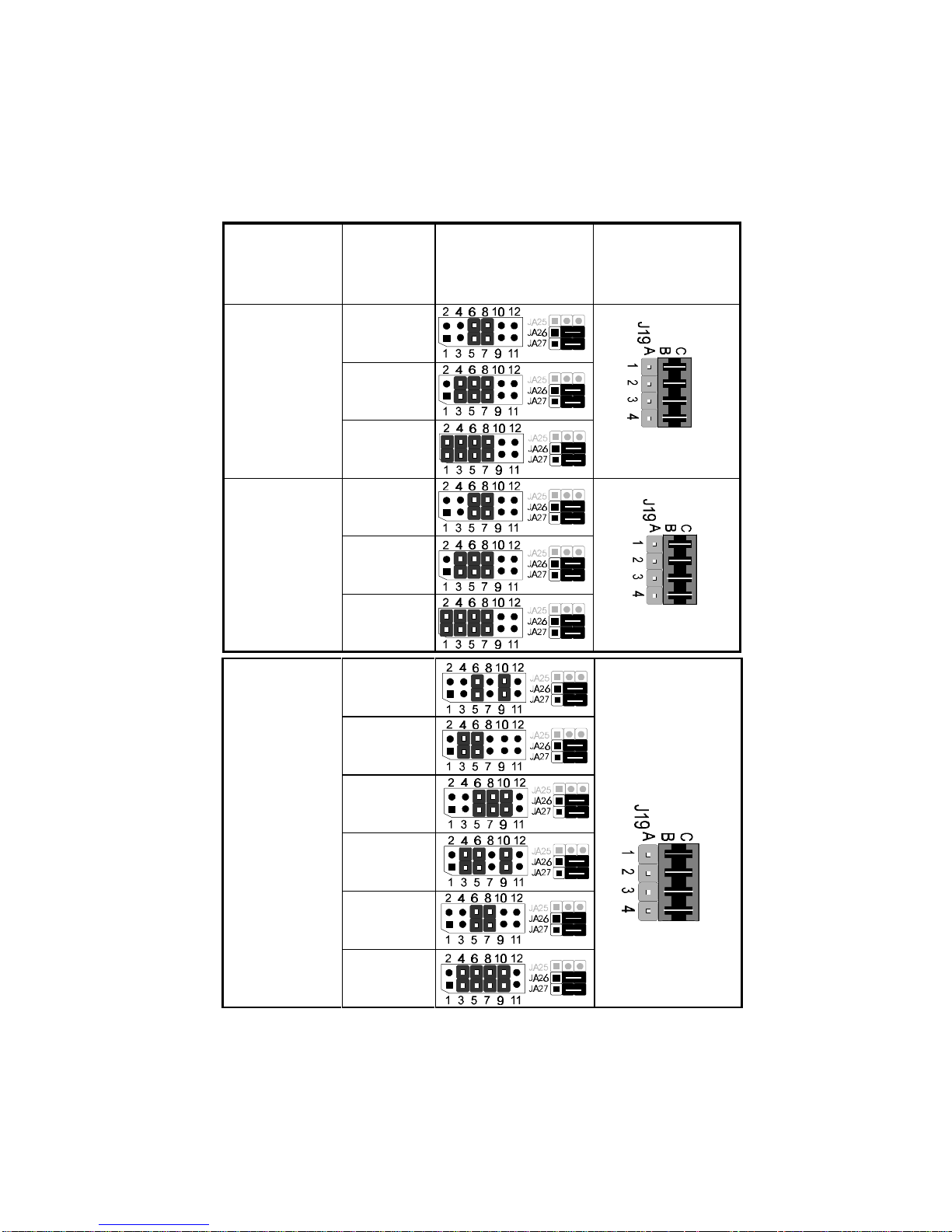
CPU Configuration - JP1, JA26, JA27 & J19
JP1, JA26, JA27 and J19 are the Jumpers that you need to set your CPU on HOT-591P. Make sure that
you know the type of CPU that you are installing and refer to the proper settings which are listed below.
Normally, CPU voltage is auto-detected on HOT-591P and is set to Auto-detected when HOT-591P is
delivered. If you have a higher frequency CPU or you want to set CPU frequency and voltage manually,
please refer to next two sections.
Intel Pentium (P54C) Series Settings
Processor Spee d
Frequency S etting
JP1, JA26, JA2 7
Jumper Bloc k J19
Vcore/Vio
Auto-detect
Intel Pentium
(P54C)
200 MHz
66MHzx3
3.3V/3.3V
166 MHz
66MHzx2.5
150 MHz
60MHzx2.5
133 MHz
66MHzx2
120 MHz
60MHzx2
100 MHz
66MHzx1.5
90 MHz
60MHzx1.5
Table 2-1
Page 11

10
Intel Pentium MMX (P55C) Series CPUs Settings
Processor Speed
Frequency Setting
JP1, JA26, JA27
Jumper Bloc k J19
Vcore/Vio
Auto-detect
Intel Pentium
MMX(P 55C)
233 MHz
66MHzx3.5
2.8V/3.3V
200 MHz
66MHzx3
166 MHz
66MHzx2.5
Table 2-2
AMD-K5 Series CPUs Settings
Processor Speed
Frequency Setting
JP1, JA26, JA27
Jumper Bloc k J19
Vcore/Vio
Auto-detect
AMD-K5
PR166
66MHzx2.5
3.52V/3.52V
PR133
66MHzx1.5
PR120
60MHzx1.5
PR100
66MHzx1.5
PR90
60MHzx1.5
Table 2-3
Page 12

11
AMD-K6 Series CPUs Settings
Processor Spee d
Frequency S etting
JP1, JA26, JP27
Jumper Block J19
Vcore/Vio
Auto-detect
AMD-K6
300 MHz
66MHzx4.5
2.2V/3.3V
266 MHz
66MHzx4
233 MHz
66MHzx3.5
233 MHz
66MHzx3.5
3.2V/3.3V
200 MHz
66MHzx3
2.9V/3.3V
166 MHz
66MHzx2.5
AMD K6-3D
300 MHz
100MHzx3
2.2V/3.3V
266 MHz
100MHzx2 .5
Table 2-4
Note :The voltage of AMD-K6 233MHz may vary from market and CPU core. Please ask your
CPU provider for detail.
Page 13
12
Cyrix/IBM 6x86/6x86L/6x86MX Series CPUs Settings
Table 2-5
Processor Speed
Fre quency Setting
JP1 , JA26 , JA27
Jumper Block J19
Vcore/Vio
Auto-detect
Cyrix/IBM
6x86L
P200+
75MHzx2
2.8V/3.3V
P166+
66MHzx2
P150+
60MHzx2
Cyrix/IBM
6x86
P200+
75MHzx2
3.52V/3.52V
P166+
66MHzx2
P150+
60MHzx2
Cyrix/IBM
6x86MX
PR266
75MHz x 3
2.9V/3.3V
PR266
66MHzx3.5
PR233
75MHzx2.5
PR233
66MHzx3
PR200
75MHzx2
PR200
66MHzx2.5
Page 14

13
IDT-C6 Series CPUs Settings
Table 2-6
Processor Speed
Frequency Setting
JP1, JA26, JA27
Jumper Bloc k J19
Vcore/Vio
Auto-detect
IDT-C6
200 MHz
66MHzx3
3.52V/3.52V
180 MHz
60MHzx3
150 MHz
60MHzx2.5
Page 15

14
System Clock and CPU Multiplier Manual Setting JP1, JA26 & JA27
Multiplier
1.5 X 2 X 2.5 X 3 X 3.5 X
JP1
P7 ~ P12
Multiplier
4 X 4.5 X 5 X 5.5 X
JP1
P7 ~ P12
Table 2-8
Figure 2-2 : Jumper JP1, JA26
and JA27 location
For whom like to set up system manually, listed tables show all the System Clock and CPU
Multiplier that HOT-591P can offer. Pin header 1~6 of JP1 and JA26, JA27 are used to
adjust System Clock from 60MHz to 100 MHz. Pin header 7~12 of JP1 are used to adjust
CPU core multiplier from 1.5X to 5.5X.
Table 2-7 shows the System Clock from 60 MHz to 100 MHz.
Table 2-8 shows CPU Multiplier from 1.5X to 5.5X.
System
Clock
60MHz 66MHz 75MHz 75MHz 83MHz 90MHz 100MHz
AGP
Clock
60MHz 66MHz 75MHz 60MHz 66MHz 60MHz 66MHz
PCI
Clock
30MHz 33MHz 37.5MHz 30MHz 33MHz 30MHz 33MHz
JP1
P1 ~ P6
JA26
JA27
Table 2-7
Page 16

15
SDRAM Frequency Setting - JA25 & JP9
HOT-591P support 100MHz external frequency AMD-K6 3D, and which allows the user to use
66MHz normal SDRAM DIMM or 100MHz PC/100 SDRAM DIMM. Jumpers JA25 and JP9
are used to set SDRAM frequency which synchronous with System Clock (CPU External Clock)
or synchronous with AGP External Clock.
This feature allows the user to use normal SDRAM with AMD-K6 3D processor.
Figure 2-4: JA25 & JP9 location
SDRAM Freque ncy Se tting
JA25, JP9
Synchronous with
System Clock
(CPU External Clock)
Synchronous with
AGP Clock
Table 2-10
Page 17

16
CPU Voltage Manual Setting - J19
HOT-591P automatically detects and adjusts the voltage
to the proper voltage.
Jumper block J19 is used to set Automatically or Manually adjust onboard voltages output from Switching type
regulators to CPU by inserting or removing mini jumper
from pin headers.
The voltage settings are made through the use of jumper
caps to connect jumper pins on the pin set 1~4 of
Jumper block J19.
Figure 2-3 : J19 Jumper Block location
Voltage J1 9 Voltage J 19
Auto
-setting
2.8 V
2.7 V
3.52 V 2.6 V
3.4 V 2.5 V
3.3 V 2.4 V
3.2 V 2.3 V
3.1 V 2.2 V
3.0 V 2.1 V
2.9 V 2.0 V
Table 2-9
Page 18

17
Power Supply Type Jumper - JP8
CMOS Clear - JP2
HOT-591P mainboard supports jumper JP2 for
discharging mainboard’s CMOS memory.
This jumper can clear the CMOS data stored
in the subsystem chip. To clear the CMOS data
please follow listed steps:
1) Turn off the PC,
2) Remove the jumper cap from JP2 pin 1-2,
3) Insert the jumper cap to JP2 pin 2-3
for a brief while,
4) Remove the jumper cap from JP2 pin 2-3,
5) Reinsert the jumper cap to JP2 pin 1-2,
6) Turn on the PC.
Figure 2-7: Clear CMOS
Jumper JP2 location
Due to different designs, there are two Power Supply Type : 12-pin AT Power Supply and
20-pin ATX Power Supply. HOT-591P support both type of Power Supply. Select the
correct type according to the Power Supply you are using.
JP8
AT/ATX P owe r S ele ction
12-Pin AT Power Supply
20-Pin ATX Power Supply
Flash EEPROM Vpp - JP5
HOT-591P mainboard supports two types of
Flash EEPROM:
5 volt and 12 volt. By setting up jumper JP5,
the main board can use both 5V or 12V flash
EEPROM with new system BIOS files as they
come available.
JP5 Pin 2-3 Close for 12V Flash EEPROM
JP5 Pin 1-2 Close for 5V Flash EEPROM
Figure 2-5: JP8 AT/ATX Power Jumper location
Table 2-11
Figure 2-6: Flash Type Jumper
JP5 location
Page 19

18
Connectors
Front Panel Connectors (JP6)
Hardware Reset Connector - RST
Attach 2-pin hardware reset switch to it. Closing the
reset switch restarts the system.
KeyLock Connector
- PW-LED Key-Lock
KeyLock & Power LED connector is a 5-pin connector
for a lock that may be installed on the system case for
enabling or disabling the keyboard. It also attached to
the case's Power LED. Pin 1 and 3 are for power LED
and pin 4 and 5 are for keylock, pin 2 is useless.
Speaker Connector - Speaker
PC speaker connector may attach a 4-pin PC speaker
cable from the case to this connector.
SMI Connector - SMI
Hardware System Management Interface connector may attach a 2-pin momentary switch to it.
When push it will force system get into power saving mode, and the system will resume when
switch is pushed again.
GLED Connector - GLED
Attach a 2-pin Green LED cable to it. The Green LED lights when the system get into power
saving mode. The Green LED off when the system resume back to normal mode.
HD LED Connector - IDE
Attach a 2-pin IDE drive LED cable to this connector. The LED lights when an IDE device is
active.
ATX Power On/Off Switch Connector - PWR_BT
Attach a 2-pin momentary type switch to this connector for turning on or off your ATX power
supply.
Figure 2-8: Front Panel Connector location
Page 20

19
Back Panel Connectors
COM1/COM2 Connectors - J9/J10
Attach COM1/COM2 connector cables to these connectors.
PS/2 Mouse Connector - J6
The main board provides a 5 pins PS/2 mouse connector for an optional PS/2
mouse cable. Diagram on the right side indicates the pinout of pin header.
HOT-591P mainboard supplies two types of optional PS/2 mouse adapter
cable, type 1 have 6-holes plug with hole 2 and hole 6 wireless; type 2
have 5 holes plug with hole 2 wireless.
Caution : When a PS/2 mouse is used, make sure connect PS/2 mouse
adapter cable hole 1 to the pin 1 of onboard PS/2 connector (J6). Reversed
connecting may cause damage to your PS/2 mouse.
Parallel Port Connector - J8
A 26-pin male pin header is located at the rear of the main board. Plug the parallel port connector cable into this connector.
USB1/USB2 Port Connectors - J14
The USB pin headers located at the rear of the board. Plug the USB
connector cable into this connector.
Other Connectors
ATX Power Supply Connector - J3
It is a twenty-pin male header connector. Plug the connector from the power directly onto the
board connector while making sure the pin 1 is in its position. The main board requires a power
supply with at least 200 watts and "power good signal.
Figure 2-9: ATX Power Supply Connector Figure 2-10: AT Power Supply Connector
Page 21

20
AT Power Supply Connectors - J2
It is a twelve-pin male header connector. Plug the connector from the power directly onto the
board connector while making sure the pin 1 is in its position. The main board requires a power
supply with at least 200 watts and "power good signal.
IR Connector - JP3
Infrared device connector may attach a 5-pin infrared device cable to this connector for enabling
the infrared transfer function. This mainboard meets the specification of ASKIR and HPSIR.
CPU, Chassis(or AGP) cooling Fan connectors - Fan1 & 2
The main board provides two onboard 12V cooling fan power connectors for CPU (Fan 2), AGP
device (Fan 1) cooling fan. Depending on the fan maker, the wiring and plug may be different.
The red wire should be connected to +12V and black wire should be connected to ground (GND)
Wake-On-LAN Connectors - J12
Attach a 3-pin connector from the LAN card which supports the Wake-On-LAN (WOL) function. This function lets users wake up the connected system through the LAN card.
( Note: Recently, only Intel LAN card support Wake-On-LAN function)
Figure 2-11: FAN 1, FAN 2 & WOL (J12) location
Page 22

21
Memory Configuration
3
3
The HOT-591P mainboard provides two 72-pin SIMM sockets and two 168-pin DIMM
sockets that make it possible to install up to 256MB of RAM. The SIMM socket support
4MB, 8MB, 16MB, 32MB, 64MB and 128MB 5V single- or double-side fast page or EDO
DRAM modules, and DIMM socket support 8MB, 16MB, 32MB, 64MB, and 128MB 3.3V
single- or double-side SDRAM, fast page, or EDO modules.
The two SIMM sockets are arranged in a single bank, the two DIMM sockets are arranged in
two banks of one socket each. Each bank provides a 64/72-bit wide data path.
Note:
Maximum memory size is 256MB total for all SIMM or DIMM sockets.
If using SIMM modules, each bank must be filled with a pair of same
modules.
The user should not populate both 5V SIMM modules & 3.3V DIMM
modules at the same time.
The memory configuration tables on next page list the SIMMs and DIMMs memory configuration.
Figure 2-12: SIMMs & DIMMs socket location
Page 23

22
SIMM 1 SIMM 2 DI MM 1 DIMM 2 TOTAL
4 MB 4 MB —— —— 8 MB
8 MB 8 MB —— —— 16 MB
16 MB 16 MB —— —— 32 MB
32 MB 32 MB —— —— 64 MB
64 MB 64 MB —— —— 128 MB
128 MB 128 MB —— —— 256 MB
—— —— 8 MB —— 8 MB
—— —— 8 MB 8 MB 16 MB
—— —— 16 MB —— 16 MB
—— —— 16 MB 16 MB 32 MB
—— —— 32 MB —— 32 MB
—— —— 32 MB 32 MB 64 MB
—— —— 64 MB —— 64 MB
—— —— 64 MB 64 MB 128 MB
—— —— 128 MB —— 128 MB
—— —— 128 MB 128 MB 256 MB
—— —— 8 MB 16 MB 24 MB
—— —— 8 MB 32 MB 40 MB
—— —— 8 MB 64 MB 72 MB
—— —— 8 MB 128 MB 136 MB
—— —— 16 MB 32 MB 48 MB
—— —— 16 MB 64 MB 80 MB
—— —— 32 MB 64 MB 96 MB
—— —— 32 MB 128 MB 160 MB
—— —— 64 MB 128 MB 192 MB
Table 2-12
Page 24

23
4
4
This chapter briefly discusses Award Flash utility provides instructions to guide you through
updating your old BIOS. The file name we use to program here is test.bin, and the file name
to save old BIOS is 591P.OLD. Please note that those file names are not absolute. They are
only examples to let you have a more clear understanding of the updating process.
How to Begin
1. Please type "awdflash" and press the ENTER key to begin the updating process.
2. Once you enter, you will see a main menu displaying:
3. Move the cursor to "File Name to Program:"
4. Type the program name "test.bin", and then press the ENTER key.
5. At the bottom of the menu, you will be requested to answer:
"Do You Want to Save BIOS (Y/N)? "
The following manual is intended to guide you through the process of both "No" and "Yes"
cases respectively.
If "No"
If you do not wish to save the old BIOS:
1. Please type "N", and then press the ENTER key.
2. Then you will be requested to answer:
"Are You Sure to Program? "
3. Answer "No" if you do not want to program, and then it will exit.
Flash Utility
Page 25

24
If "Yes"
To save the old BIOS:
1. Please respond "Y", and then press the ENTER key.
2. Move the cursor to "File Name to Save: "
3. Type file name "591P.OLD", and then press the ENTER key. (Your old BIOS will be
saved in the file name you create. In this case, the old BIOS is saved in the file name,
591P.OLD).
4. Then you will be requested to answer:
"Are You Sure to Program (Y/N)? "
5. Type "Y" to begin programming, and press the ENTER key.
6. When the programming is finished, the showing message will appear:
7. Once you see the showing message "Power Off or Reset System", please restart
your system.
8. When you power on the computer again, you will find your old BIOS has already
been successfully updated.
To view a complete usage of FLASH utility, please type "awdflash /?" and press the
ENTER key.
Notes About Award Flash Utility
Please note that Award Flash Utility cannot run under EMM386 or QEMM. Thus, when
executing the command "awdflash", an error message will appear:
"Error Message: Failure Due to EMM386 or QEMM !"
Page 26

25
VIA VxD AGP Driver Installation
5
5
This section describe the installation of VIA VxD Driver which supports Accelerated
Graphics Port (AGP) functionalists.
System Requirements
This driver should be installed on a system with the HOT-591P main board which based on
VIA AGP chipset VT82C598AT MVP3, and others’ main board will not be supported.
The VIA VGART Driver is only supported by Windows 95 OSR 2.1 (4.00.950 B) or later
version.
You may find the VGART Driver on attached CD-ROM in \Driver\VGART directory.
For Win95 users, you will need to
1. Get “USBSUPP.EXE” from Microsoft, which includes the USB supplement and a
new memory manager (VMM32.VxD) needed for the AGP DIME (Direct Memory
Execute) feature.
2. Get DirectX 5.0 from Microsoft. DirectX 5.0 is the first DirectX version that supports
AGP’s DIME.
3. Get AGP Master (i.e., AGP VGA) Driver from VGA Supplier.
4. Install “VIAGART.VXD”, VIA Graphics Address Remapping Table Driver from
attached CD-ROM.
For WinNT 4.0 users, you need to install Microsoft Windows NT Service Pack 3.0 before
install AGP Masster Driver, or you will have to wait until WinNT 5.0 is released.
Installation Instructions
Run program “SETUP.EXE” in the directory of \Driver\VGART\VIA on attached CDROM, and it will install the VIA VGART Driver automatically onto your Windows 95
system.
Page 27

26
BIOS Setup
6
6
HOT-591P BIOS ROM has a built-in Setup program that allows users to modify the basic
system configuration. This type of information is stored in battery-backed RAM so that it
retains the Setup information when the power is turned off.
Entering Setup
Power on the computer and press <Del> immediately will allow you to enter Setup. The
other way to enter Setup is to power on the computer, when the below message appear briefly
at the bottom of the screen during the POST (Power On Self Test), press <Del> key or
simultaneously press <Ctrl>,<Alt>, and <Esc> keys.
“Press DEL to enter SETUP”
If the message disappears before you respond and you still wish to enter Setup, restart the
system to try again by turning it OFF the ON or pressing the “RESET” button on the system
case. You may also restart by simultaneously press <Ctrl>,<Alt>, and <Delete> keys. If you
do not press the keys at the correct time and the system does not boot, an error message will
be displayed and you will again be asked to,
“Press F1 to Continue, DEL To Enter Setup”
Page 28

27
Standard CMOS setup
This setup page includes all items in a standard compatible BIOS.
BIOS features setup
This setup page includes all items of Award special enhanced features.
Chipset features setup
This setup page includes all items of chipset features.
Power Management Setup
This setup page includes all items of Power Management features.
PnP/PCI Configuration
This item specifies the value (in units of PCI bus blocks) of the latency timer for the
PCI bus master and the IRQ level for PCI device. Power-on with BIOS defaults
Load BIOS Defaults
BIOS defaults loads the values required by the System for the maximum performance.
However, you can change the parameter through each Setup Menu.
Load Setup Defaults
Setup defaults loads the values required by the system for the O.K. performance.
However, you can change the parameter through each Setup Menu.
Main Menu
Page 29

28
Integrated Peripherals
This setup page includes all items of peripheral features.
Supervisor Password
Change, set, or disable supervisor password. It allows you to limit access to the system
and Setup, or just to Setup.
User Password
Change, set, or disable user password. It allows you to limit access to the system and
Setup, or just to Setup.
IDE HDD auto detection
Automatically configure IDE hard disk drive parameters.
Save & Exit setup
Save CMOS value change to CMOS and exit setup
Exit without saving
Abandon all CMOS value changes and exit setup.
Page 30

29
Date
The date format is <day>, <month> <date> <year>. Press <F3> to show the calendar.
Time
The time format is <hour> <minute> <second>. The time is calculated base on the 24hour military-time clock. For example. 5 p.m. is 17:00:00.
Hard Disks Type
This item identify the types of hard disk drives that has been installed in the computer.
There are 46 predefined types and a user definable type.
Press PgUp or PgDn to select a numbered hard disk type or type the number and press
<Enter>. Note that the specifications of your drive must match with the drive table.
The hard disk will not work properly if you enter improper information for this item.
If your hard disk drive type is not matched or listed, you can use Type User to define
your own drive type manually.
If you select Type User, related information is asked to be entered to the following
items. Enter the information directly from the keyboard and press <Enter>. Those
information should be provided in the documentation from your hard disk vendor or the
system manufacturer.
The user may also set those items to AUTO to auto configure hard disk drives parameter when system power-on.
If a hard disk drive has not been installed select NONE and press <Enter>.
Standard CMOS Setup
Page 31

30
Drive A type/Drive B type
This item specifies the types of floppy disk drive A or drive B that has been installed in
the system.
Video
This item selects the type of adapter used for the primary system monitor that must
matches your video display card and monitor. Although secondary monitors are supported, you do not have to select the type in Setup.
Error halt
This item determines if the system will stop, when an error is detected during power up.
Memory
This item is display-only. It is automatically detected by POST (Power On Self Test) of
the BIOS.
Base Memory
The POST of the BIOS will determine the amount of base (or conventional) memory
installedin the system. The value of the base memory is typically 512K for systems with
512K memory installed on the mainboard, or 640K for systems with 640K or more memory
installed on the mainboard.
Extended Memory
The BIOS determines how much extended memory is present during the POST. This is the
amount of memory located above 1MB in the CPU’s memory address map.
Page 32

31
Virus Warning
When this item is enabled, the Award BIOS will monitor the boot sector and partition
table of the hard disk drive for any attempt at modification. If an attempt it made, the
BIOS will halt the system and the following error message will appear. Afterwards, if
necessary, you will be able to run an anti-virus program to locate and remove the
problem before any damage is done.
CPU Internal/External Cache
This item enables CPU internal cache and external cache to speed up memory access.
Quick Power On Self Test
This item speeds up Power On Self Test (POST) after you power on the computer.
If it is set to Enabled, BIOS will shorten or skip some check items during POST.
Boot Sequence
This item determines which drive computer searches first for the disk operating system.
Default setting is A, C, SCSI.
BIOS also support system boot from CD-ROM drive or SCSI hard disk drive.
BIOS Features Setup
Page 33

32
Swap Floppy Drive
When this item enables, the BIOS will swap floppy drive assignments so that Drive A:
will function as Drive B: and Drive B: as Drive A:.
Boot Up Floppy Seek
During POST, BIOS will determine if the floppy disk drive installed is 40 or 80 tracks.
Boot Up NumLock Status
When this option enables, BIOS turns on Num Lock when system is powered on.
Boot Up System Speed
This option sets the speed of CPU at system boot time. The settings are High or Low.
Gate A20 Option
This entry allows you to select how the gate A20 is handled. The gate A20 is a device
used to address memory above 1 Mbytes. Initially, the gate A20 was handled via a pin
on the keyboard. Today, while keyboards still provide this support, it is more common,
and much faster, set to Fast for the system chipset to provide support for gate A20.
Memory Parity/ECC Check
This item allows you to set memory error checking, Enabled or Disabled.
Typematic Rate Setting/Typematic Rate/Typematic Delay
This determines if the typematic rate and typematic delay are to be used. When the
typematic rate setting is enabled, typematic rate allows you select the rate at which the
keys are accelerated and typematic delay allows you to select the delay between when
the key was first depressed and when the acceleration begins.
Security Option
This item allows you to limit access to the System and Setup, or just to Setup.
When System is selected, the System will not boot and access to Setup will be denied if
the correct password is not entered at the prompt.
When Setup is selected, the System will boot, but access to Setup will be denied if the
correct password is not entered at the prompt.
PCI / VGA Palette Snoop
This item must be set to enabled if there is a MPEG ISA card installed in the system,
and disabled if there is no MPEG ISA card installed in the system.
OS Select For DRAM > 64MB
This item allows you to access the memory that over 64 MB in OS/2.
Video BIOS Shadow/XXXXX-XXXXX Shadow
These items determine whether Video BIOS or optional ROM will be copied to RAM.
Page 34

33
Chipset Features Setup
Bank x/x DRAM Timing
This value in this field is set by the system board manufacturer, depending on whether
the board has paged DRAMs or EDO DRAMS.
The choice: 70ns, 60ns.
SDRAM Cycle Length
This field allows you to set the SDRAM latency timer.
The Choice: 2, 3.
SDRAM Bank Interleave
This item allows you to set how many banks of SDRAM support in your mainboard.
The Choice: 2 Bank, 4 Bank, Disabled.
DRAM Read Pipeline
This item allows you to set DRAM Read Pipeline function Enabled or Disabled.
Sustained 3T Write
This item allow you to enable or disable direct map write back / write through secondary cache.
The Choice: Enabled, Disabled.
Cache Rd+CPU Wt Pipeline
This item allows you to enable/disable the cache timing.
The Choice: Enabled, Disabled.
Read Around Write
This item allows you enable/disable the read around write function (system performance timing)
The Choice: Enabled, Disabled.
Page 35

34
Cache Timing
This item allows the user to set the cache timing. The options are Fast and Fastest.
Video BIOS Cacheable
When enabled. The Video BIOS cache will cause access to video BIOS addressed at
C0000H to C7FFFH to be cached, if the cache controller is also enabled.
The Choice: Enabled, Disabled.
System BIOS Cacheable
As with caching the Video BIOS above, enabling this selection allows accesses to the
system BIOS ROM addressed at F0000H ~ FFFFFH to be cached, provided that the cache
controller is enabled.
The Choice: Enabled, Disabled.
Memory Hole At 15MB Addr
In order to improve performance, some space in memory can be reserved for ISA cards.
This memory must be mapped into the memory space below 16 MB.
This Choice: Disabled, 15M-16M.
AGP Aperture Size
Select the size of Accelerated Graphics Port (AGP) aperture. The aperture is a portion of
the PCI memory address range dedicated for graphics memory address space. Host cycles
that hit the aperture range are forwarded to the AGP without any translation.
See www.apgforum.org for AGP information.
The Choice: 4M, 8M, 16M, 32M, 64M, 128M, 256M
AGP-2x Mode
This item allows you to enable/disable AGP-2x function. See www.apgforum.org for AGP
information.
The Choice: Enabled, Disabled.
CPU Core Voltage
Since the mainboard support CPU voltage auto-detecting and setting, this item allows the
user to enable this function when set to Auto. The user can also set CPU core voltage
manually in BIOS from 2.1V to 3.5V.
OnChip USB
Select Enabled if your system contains a Universal Serial Bus (USB) controller and you
have a USB peripheral.
The Choice: Enabled, Disabled.
USB Keyboard Support
Select Enabled if your system contains a Universal Serial Bus (USB) controller and you
have a USB Keyboard.
The Choice: Enabled, Disabled.
Spread Spectrum Modulated
This item allows the user to enable Spread Spectrum Modulated to reduce the EMI.
The Choice: 1.5%(NTR), 0.6%(CNTR), 1.5%(Down), 0.6%(Down) and Disabled.
Page 36

35
Power Management
This item determines the options of the power management function. Max Saving puts
the system into power saving mode after a brief period of system inactivity; Min
Saving is the same as Max Saving except the time of the system inactivity period is
longer; Disabled disables the power saving feature; User Defined allows you to set
power saving options according to your preference.
PM Control by APM
When enabled, and Advanced Power Management device will be activated to enhance
the Max. Power Saving mode and stop the CPU internal clock. If Advance Power
Management (APM) is installed on your system, selecting Yes give better power
savings.
If the Max. Power Saving is not enabled, this will be preset to No.
Video Off Option
When enabled, this features allows the VGA adapter to operate in a power saving
mode.
Always On : Monitor will remain on during power saving modes.
Suspend-->Off : Monitor blanked when the systems enters the Suspend mode.
Susp, Stby-->Off : Monitor blanked when the system enters either Suspend or Standby
modes.
All Modes-->Off : Monitor blanked when the system enters any power saving mode.
Power Management Setup
Page 37

36
Video Off Method
This determines the manner in which the monitor is blanked.
V/H SYNC+Blank This selection will cause the system to turn off the vertical and
horizontal synchronization ports and write blanks to the video buffer.
Blank Screen This option only writes blanks to the video buffer.
DPMS Allows the BIOS to control the video display card if it supports the DPMS
feature.
MODEM Use IRQ
This determines the IRQ in which the MODEM can use.
The choice: 3, 4, 5, 7, 9, 10, 11, NA.
Soft-Off by PWRBTN
When Enabled, turning the system off with the on/off button places the system in a very
low-power-usage state, with only enough circuitry receiving power to detect power
button activity or Resume by Ring activity.
The choice: Delay 4 Sec, Instant Off.
HDD Power Down
When enabled and after the set time of system inactivity, the hard disk drive will be
powered down while all other devices remain active.
Doze Mode, Suspend Mode
These items set the period of time after which each of these mode activate, the periods
are from 10sec to 1 hour.
Doze Mode When enabled and after the set time of system inactivity, CPU clock will
run at slower speed while all other devices still operate at full speed.
Suspend Mode When enabled and after the set time of system inactivity, all devices
except CPU will be shut off.
** PM Events **
PM events are I/O events whose occurrence can prevent the system from entering a
power saving mode or can awaken the system from such a mode. In effect, the system
remains alert for anything occurs to a device which is configured as On, even when the
system is a power down mode.
VGA
When set to On (default), any event occurring at a VGA port will awaken a system
which has been powered down.
LPT & COM
When set to LPT/COM (default), any event occurring at a COM (Serial)/LPT port will
awaken a system which has been powered down.
HDD & FDD
When set to On (default), any event occurring at a hard or floppy drive port will awaken
a system which has been powered down.
Page 38

37
DMA/master
When set to On (default), any event occurring to the DMA controller will awaken a
system which has been powered down.
Modem Ring /LAN Resume
When set to Enabled, any event occurring Modem Ring/activity of LAN will awaken a
system which has been powered down.
Note : The mainboard support Wake-ON-LAN function with Intel LAN card only.
RTC Alarm Resume
When set to Enabled RTC Alarm Resume, you could set the date (of month) and timer
(hh:mm:ss), any event occurring at RTC will awaken system which has been powered
down.
Primary INTR
When set to On (default), any event occurring at will awaken a system which has been
powered down.
The following is a list of IRQ, Interrupt ReQuests, which can be exampled much as the
COM ports and LPT port above can. When an I/O device wants to gain the attention of
the operating system, it signals this by causing an IRQ to occur. When the operating
system is ready to respond to the request, it interrupts itself and performs the service.
As above, the choices are On and Off.
When set On, activity will neither prevent the system from going into a power manage-
ment mode nor awaken it.
- IRQ3 (COM 2) - IRQ4 (COM 1)
- IRQ5 (LPT 2) - IRQ6 (Floppy Disk)
- IRQ7 ( LPT 1) - IRQ8 (RTC Alarm)
- IRQ9 (IRQ2 Redir) - IRQ10 (Reserved)
- IRQ11 (Reserved) - IRQ12 (PS/2 Mouse)
- IRQ13 (Coprocessor) - IRQ14 (Hard Disk)
- IRQ15 (Reserved)
Page 39

38
PNP OS Installed
When this item is set to Yes, it will allow the PnP OS(Windows 95) control the system
resources except PCI devices and PnP boot devices.
The Choice: Yes and No.
Resources Controlled By
The Award Plug and Play BIOS has the capability to automatically configure all of the
boot and Plug and Play compatible devices. However, this capability means absolutely
nothing unless you are using a Plug and Play operating system as Windows 95.
The Choice: Auto and Manual.
Reset Configuration Data
Normally, you leave this field Disabled. Select Enabled to reset Extended System
Configuration Data (ESCD) when you exit Setup if you have installed a new add-on
and the system reconfiguration has caused such a serious conflict that the operating
system can not boot.
The Choice: Enabled and Disabled.
ACPI I/O Device Node
This item allows the user to set ACPI I/O Device Node Enabled or Disabled.
IRQ 3/4/5/7/9/10/11/12/14/15, assigned to
When resources are controlled manually, assign each system interrupt as one of the
following types, depending on the type of device using the interrupt:
Legacy ISA Devices compliant with the original PC AT bus specification, requiring a
specific interrupt (such as IRQ4 for serial port 1). PCI/ISA PnP Devices compliant
with the Plug and Play standard, whether designed for PCI or ISA bus architecture.
The Choice: Legacy ISA and PCI/ISA PnP.
PCI Configuration Setup
Page 40

39
DMA 0/1/3/5/6/7 assigned to
When resources are controlled manually, assign each system DMA as one of the following
types, depending on the type of device using the interrupt:
Legacy ISA Devices compliant with the original PC AT bus specification, requiring a
specific interrupt (such as IRQ4 for serial port 1). PCI/ISA PnP Devices compliant with
the Plug and Play standard, whether designed for PCI or ISA bus architecture.
The Choice: Legacy ISA and PCI/ISA PnP.
These items allow you to determine the DMA assigned to the ISA bus and is not available
for PCI slot.
The Choice: Legacy ISA and PCI/ISA PnP.
CPU to PCI Write Buffer
When enabled, up to four Dwords of data can be written to the PCI bus without interrupting
the CPU. When disabled, a write buffer is not used and the CPU read cycle will not be
completed until the PCI bus signals that it is ready to receive the data.
The choice: Enabled, Disabled.
PCI Dynamic Bursting
When Enabled, data transfers on the PCI bus, where possible, make use of the highperformance PCI burst protocol, in which greater amounts of data are transferred at a single
command.
The choice: Enabled, Disabled.
PCI Master 0 WS Write
When Enabled, writes to the PCI bus are command with zero wait states.
The choice: Enabled, Disabled.
PCI Delay Transaction
The chipset has an embedded 32-bit posted write buffer to support delay transactions
cycles. Select Enabled to support compliance with PCI specification version 2.1.
The choice: Enabled, Disabled.
PCI Master Read Prefetch
This item allows you enable/disable the PCI Master Read Prefetch.
The choice: Enabled, Disabled.
PCI #2 Access #1 Retry
This item allows you enable/disable the PCI #2 Access #1 Retry.
The choice: Enabled, Disabled.
AGP Master 1 WS Write
This implements a single delay when writing to the AGP Bus. By default, two-wait states
are used by the system, allowing for greater stability.
The choice: Enabled, Disabled.
AGP Master 1 WS Read
This implements a single delay when reading from the AGP Bus. By default, two-wait
states are used by the system, allowing for greater stability.
The choice: Enabled, Disabled.
Page 41

40
PCI IRQ Activated by
This item sets the method by which the PCI bus recognize that an IRQ service is being
requested by a device. You should never change the default configuration unless advised
otherwise by your System's manufacturer.
The Choice: Level(default) and Edge.
PCI Latency Timer
The number of clocks programed in the PCI Latency Timer represents the guaranteed time
slice allocated to the 82C598AT, after which it must complete the current data transfer
phase and surrender the bus as soon as its bus grant is removed.
The PCI Latency Timer is used to guarantee to the PCI agents a minimum amount of the
system resource.
The default setting is 64 PCI clocks.
Assign IRQ For VGA
This item allows the user to set VGA IRQ Routing table Enabled or Disabled.
Page 42

41
OnChip IDE First Channel
This item is used to defined on chip Primary PCI IDE controller is Enable or Disable
setting.
OnChip IDE Second Channel
This item is used to defined on chip secondary PCI IDE controller is Enable or Disable
setting.
IDE Prefetch Mode
Enable prefetching for IDE drive interfaces that support its faster drive accesses. If you
are getting disk drive errors, change the setting to omit the drive interface where the
errors occur. Depending on the configuration of your IDE subsystem, this field may not
appear, and it does not appear when the Internal PCI/IDE field, above, is Disabled.
The choice: Enabled, Disabled.
IDE HDD Block Mode
This item is used to set IDE HDD Block Mode. If your IDE Hard Disk supports block
mode, then you can enable this function to speed up the HDD access time. If not,
please disable this function to avoid HDD access error.
IDE Primary Master PIO
In these items, there are five modes defined in manual mode and one automatic mode.
There are 0, 1, 2, 3, 4, and AUTO is the default settings for on board Primary Master
PIO timing.
Integrated Peripherals
Page 43

42
IDE Primary Slave PIO
In these items, there are five modes defined in manual mode and one automatic mode.
There are 0, 1, 2, 3, 4, and AUTO is the default settings for on board Primary Slave
PIO timing.
IDE Secondary Master PIO
In these items, there are five modes defined in manual mode and one automatic mode.
There are 0, 1, 2, 3, 4, and AUTO is the default settings for on board Secondary Master
IDE PIO timing.
IDE Secondary Slave PIO
In these items, there are five modes defined in manual mode and one automatic mode.
There are 0, 1, 2, 3, 4, and AUTO is the default settings for on board Secondary Slave
IDE PIO timing.
IDE Primary Master UDMA
On this mainboard, VIA chipset improves IDE transfer rate using Bus Master
UltraDMA/33 IDE which can handle data transfer up to 33MB/sec. The options are
Disabled and Auto, and Auto is the default settings for on board Primary Master
UltraDMA33.
IDE Primary Slave UDMA
On this mainboard, VIA chipset improves IDE transfer rate using Bus Master
UltraDMA/33 IDE which can handle data transfer up to 33MB/sec. The options are
Disabled and Auto, and Auto is the default settings for on board Primary Slave
UltraDMA33.
IDE Secondary Master UDMA
On this mainboard, VIA chipset improves IDE transfer rate using Bus Master
UltraDMA/33 IDE which can handle data transfer up to 33MB/sec. The options are
Disabled and Auto, and Auto is the default settings for on board Secondary Master
UltraDMA33.
IDE Secondary Slave UDMA
On this mainboard, VIA chipset improves IDE transfer rate using Bus Master
UltraDMA/33 IDE which can handle data transfer up to 33MB/sec. The options are
Disabled and Auto, and Auto is the default settings for on board Secondary Slave
UltraDMA33.
Onboard FDC Controller
This item specifies onboard floppy disk drive controller. This setting allows you to
connect your floppy disk drives to the onboard floppy connector. Choose the
“Disabled” settings if you have a separate control card.
Onboard Serial Port 1/2
This item is used to define onboard serial port 1/Port2 to 3F8/IRQ4, 2F8/IRQ3, 3E8/
IRQ4, 2E8/IRQ3, Auto or Disabled.
Page 44

43
UR2 Mode
The main board support IrDA(HPSIR) and Amplitudes Shift Keyed IR(ASKIR)
infrared through COM2 port. When IR is enable, the onboard COM2 port will be
disabled. This item specifies onboard Infra Red mode to IrDA 1.0, ASKIR, MIR
0.57M, MIR 1.15M, FIR or Standard (Disabled).
Note : FIR is not supported currently.
IR Mode
This item is to select the value required by the IR device connected to the IR port. Fullduplex mode permits simultaneous two-direction transmission. Half-duplex mode
permits transmission in one direction only at a time.
Onboard Parallel Port
This item specifies onboard parallel port address to 378H, 278H, 3BCH or Disabled.
Parallel Port Mode
This item specifies onboard parallel port mode. The options are SPP (Standard Parallel
Port), EPP (Enhanced Parallel Port), ECP (Extended Capabilities Port), and EPP+ECP.
ECP Mode Use DMA
This item specifies DMA (Direct Memory Access) channel when ECP device is in use.
The options are DMA 1 and DMA 3. This item will not show up when SPP and EPP
printer mode is selected.
Page 45

44
Password Setting
This section describes the two access modes that can be set using the options found on the
Supervisor Password and User Password.
Supervisor Password and User Password
The options on the Password screen menu make it possible to restrict access to the Setup
program by enabling you to set passwords for two different access modes: Supervisor
mode and User mode.
In general, Supervisor mode has full access to the Setup options, whereas User mode has
restricted access to the options. By setting separate Supervisor and User password, a
system supervisor can limit who can change critical Setup values.
Enter Password
Type the password, up to eight characters, and press <Enter>. The password typed now
will clear any previously entered password from CMOS memory. You will be asked to
confirm the password. Type the password again and press <Enter>. You may also press
<Esc> to abort the selection and not enter a password.
To disable password, just press <Enter> when you are prompted to enter password. A
message will confirm the password being disabled. Once the password is disabled, the
system will boot and you can enter Setup freely.
Password Disable
If you select System at Security Option of BIOS Features Setup Menu , you will be
prompted for the password every time the system is rebooted or any time you try to enter
Setup. If you select Setup at Security Option of BIOS Features Setup Menu, you will be
prompted only when you try to enter Setup.
Warning : Retain a record of your password in a safe place. If you forget the password,
the only way to access the system is to clear CMOS memory, please refer to “Clear
CMOS”.
 Loading...