

Page 1
Shure Incorporated
222 Hartrey Avenue
Evanston IL 60202-3696 U.S.A.
LX Wireless System
SERVICE MANUAL CHANGE NOTICE
LX2 WIRELESS HAND-HELD TRANSMITTER
Changes and c orrections h ave b een made t o t he S ervice M anual f or t he L X2 H and-Held Transmitter. To u pdate your Service M anual, r emove t he p ages i dentified i n t he t ables b elow a nd r eplace t hem w ith t he p ages
attached to this Change Notice. Not e that there are no changes to pages not specifically identified in the
tables below.
LX2 HAND-HELD TRANSMITTER SERVICE MANUAL REVISION HISTORY
Release Part Number Date Code
Original 25A1006 QH
Revision 1 25B1006 QL
Revision 2 25C1006 SC
Revision 3 25D1006 SI
Revision 4 25D1006 TF
Revision 5 25D1006 BB
Revision 6 25D1006 BK
Revision 7 25D1006 CG
CHANGES EFFECTIVE JULY 10, 2003
REMOVE
these pages from the
LX2 Service Manual
these new Revision pages into the
INSERT
LX2 Service Manual
35 35
E1999, Shure Incorporated Printed in U.S.A.
25–1006–1 (CG)
Page 2
LX2 Hand-Held Transmitter
ÁÁÁÁÁÁ
ÁÁ
ÁÁÁ
ÁÁÁÁÁ
ÁÁ
ÁÁÁÁÁÁÁ
Á
Characteristics
General
The Shure LX2 Hand-Held Transmitter is part of a wireless system
designed for public address, educational radio and television broadcasting, school and community theater productions, and similar applications.
The LX2 is intended for use with the matching LX3 and LX4 receivers.
Controls and Connectors
Service Manual
25D1006 (CG)
1
LX2/BETA 58
6
5
2
3
BAT
4
MUTE
Figure 1. Identification of Controls and Connectors
1. Grille
2. OFF/PWR power switch
3. Battery LEDs
4. ON/MUTE mic switch
5. Audio gain control
6. Battery cup
Service Note: Shure recommends that all service procedures
be performed by a Factory-Authorized Service Center or that the
product be returned directly to Shure Brothers Inc.
E1999, Shure, Inc.
Printed in U.S.A.
25D1006 (CG)
Licensing: Operation may require a user license. Frequency or
power-output modifications may violate this product’s approvals.
Contact your country’s communications authorities.
Characteristics1
Page 3

Shure LX2 Hand-Held Transmitter
Circuit Description
The Shure LX2 Hand-Held Transmitter contains three circuit boards;
an audio section, an rf section, and a microphone head interface board.
It is intended for use with the matching LX3 and LX4 receivers.
Audio Section
Audio signals from the microphone head enter the transmitter via a
printed circuit board (pcb) with spring contacts, which also interconnects
the audio and rf printed circuits.
The audio signal next enters a preamplifier stage consisting of
one section of operational amplifier (U102C). The voltage gain of this
stage may be adjusted over a 40 dB range by means of an externallyaccessible potentiometer (R125) to enable the user to compensate for
variations in sound level at the microphone.
The preamplified audio signal is then passed through a passive
pre-emphasis network consisting of R142, C110, C111, R112, and R115,
that has a pole at 63 microseconds and a zero at 12 microseconds.
Audio Signal Compression
The signal then enters the NE571D integrated circuit compander
(U101A). This provides 2:1 logarithmic compression of the audio signal.
A lower noise floor is achieved by U102A. An internal potentiometer
(R130) is provided for nulling system audio distortion. Operational
amplifier U102B operates as a two-pole active low-pass filter to restrict
the bandwidth of the system to audio frequencies.
Reverse Battery Protection and Low Battery Warning
The NE571D also contains an identical second channel (U101B),
which in this case is used to supply regulated, low-noise 5 Vdc bias to
various audio and rf circuit points. Transistor Q105 provides reverse
battery protection to the circuit. Q110 drives a green LED (D103) that
serves as a power ON indicator. Q107 drives an amber LED (D102)
that provides a low battery warning signal to the user. Q106 and Q108
drive a red LED (D101) that serves as a final low battery indicator.
Rf: Domestic (FCC/IC)
Processed audio enters R201, an internal potentiometer that is
adjusted for 15 kHz deviation (100% modulation) with a –2.2 dBV, 1 kHz
tone at the output of the audio section. The audio is then fed to varactor
diode D201, which is part of the modulated oscillator-tripler stage (Q201).
Characteristics
2
25D1006 (CG)
Page 4

Shure LX2 Hand-Held Transmitter
The base-emitter circuit of Q201 operates as a crystal-controlled
Colpitts oscillator in the 20 MHz region. Fundamental-mode crystal Y201
is tuned 10 kHz below series resonance by the series combination of
frequency-netting coil L201, diode D201, capacitor C203, and capacitor
divider C206 and C207.
Frequency Stability
To ensure frequency stability with changes in battery voltage,
regulated 5 Vdc bias is applied to the varactor diode and to the base
of Q201. Temperature compensation is provided by C206 and C207.
The collector circuit of Q201 is tuned to the third harmonic of the
oscillator frequency (approximately 60 MHz) by means of L202 and
C208. C210 couples rf energy to a second tuned circuit consisting
of L203, C214, and C215, which also forms a capacitively-tapped
voltage divider for matching into the base of Q202, operating as a
buffer amplifier.
Regulated dc bias is again employed to minimize changes in loading
on the oscillator stage and stabilize drive levels. The collector circuit of
Q202 is again tuned to the third harmonic of the oscillator frequency by
L204 and C216. C219 couples rf energy to another tuned circuit consisting of L205, C222, and C224, which also forms a capacitively-tapped
voltage divider for matching into the base of Q203.
Frequency Tripler
The third stage (Q203) is operated as a frequency tripler with the
collector circuit tuned to the output frequency (for example, 180 MHz).
In this case L206, C226, C229, L207, C230, and C232 perform tuning
and impedance matching functions. As in the preceding stage, regulated
dc bias is applied to the base circuit to stabilize the drive level, and the
output is double-tuned to provide spectral purity.
The final output stage (Q204) is operated as a tuned amplifier.
Resistive loading on the input enhances stability. The output circuit
consists of a tuned tank circuit (L209, C237, and C239) which also
provides impedance matching to the output low-pass filter (C239,
L210, and C241). L211 and C242 match the antenna to the filter.
Stable Operation
To promote stable operation, the LX2 is designed to minimize the
production and radiation of spurious emissions and harmonic energy.
In addition to the features described previously, the collector of each rf
stage is separately decoupled from the 9 Vdc supply using ferrite chokes,
resistors, and bypass capacitors of the appropriate value. The base circuits are similarly decoupled except that they use resistor–capacitor
(R–C) networks that are more appropriate, due to the higher impedance
level. The use of surface mount components results in better performance because of a reduction in stray inductances and unwanted
radiation from component leads. Double-sided printed circuit board
construction improves ground–plane performance.
25D1006 (CG)
Characteristics3
Page 5

Shure LX2 Hand-Held Transmitter
Rf: Euro (ETSI)
Audio Input
Processed audio enters R201, an internal potentiometer that is
adjusted for 15 kHz deviation (100% modulation) when the audio
section provides a –2.2 dBV, 1 kHz tone.
Oscillation
The audio then goes to varactor diode D201, which is part of the
modulated oscillator-tripler stage (Q201). The latter’s base-emitter circuit
operates as a crystal-controlled Colpitts oscillator in the 20 MHz region.
Fundamental-mode crystal Y201 is tuned 10 kHz below series resonance
by the series combination of frequency-netting coil L201, diode D201,
capacitor C203, and capacitor divider C206 and C207.
Frequency Stability
To ensure frequency stability despite changes in the battery voltage,
regulated 5 Vdc bias is applied to the varactor diode and to the base of
Q201. C203, C206, and C207 provide temperature compensation.
Tuned Circuits
Stage 1: The collector circuit of Q201 is tuned to the third harmonic
of the oscillator frequency (approximately 60 MHz) by L202, C208, C244,
C210, L203, C214, C213, and C215. The latter components also form a
capacitively-tapped voltage divider for matching into the base of Q202.
The output is double-tuned to provide high spectral purity. Regulated dc
bias is again employed to minimize changes in loading on the oscillator
stage and to stabilize the drive levels.
Stage 2: Q202 operates as a buffer with the collector circuit tuned to
the output frequency (for example, 60 MHz). In this case, L204, C216,
C245, C218, L205, C222, C221, and C224 perform tuning and impedance-matching functions. As in the preceding stage, regulated dc bias
is applied to the base circuit to stabilize the drive level, and the output
is double-tuned to provide spectral purity.
Stage 3: Q203 operates as a frequency tripler, with the collector
circuit tuned to the output frequency (for example, 180 MHz). In this
case, L206, C226, C227, C229, L207, C230, and C232 perform tuning
and impedance-matching.
Stage 4: Q204 operates as a tuned amplifier. Resistive loading on
the input provides stability. The output circuit consists of a resonant tank
circuit (L203 and C213) capacitively coupled to a low-pass filter (C219,
L206, and C218). C213 and C219 provide a capacitively-tapped voltage
divider for matching into the low-pass filter.
Characteristics
4
25D1006 (CG)
Page 6

Shure LX2 Hand-Held Transmitter
Final Output
Transmitter: The transmitter can deliver up to +11.5 dBm (14 mW)
to the antenna. No user adjustments permit this value to be exceeded.
Testpoint TP6 provides a termination point for the 50 Ω output. C243 and
L211 act as a series-resonating network for the battery, which acts as the
antenna. The unit should be powered exclusively by a 9 Vdc dry battery.
An alkaline type such as the Duracell MN1604 is recommended.
Voltage Measurements
With 9 Vdc applied to the unit, the following voltages should appear
at the terminals of the output transistor:
S Vc = 8.83 Vdc
S Vb = .097 Vdc
S Ve = .32 Vdc
S Base current = 0.27 µAdc
S Emitter current = 9.67 mAdc
S Collector current = 9.67 mAdc
S Power input = 87 mW
The output power is +9.5 dBm (8.9 mW) into a 50 Ω load, at a
frequency of 169.445 MHz. At the lowest acceptable battery voltage
of 6 Vdc, the final collector current drops to 8.84 mAdc and the output
power to +7.3 dBm (5.4 mW).
Power Section
Spurious Emissions
To promote stable operation and to minimize the production and
radiation of spurious emissions and harmonic energy, the collector of
each rf stage is separately decoupled from the 9 Vdc supply by ferrite
chokes, resistors, and bypass capacitors. The base circuits are similarly
decoupled, except for using resistor-capacitor (R-C) networks whose
higher-impedance levels are more appropriate.
The transmitter delivers a maximum of +3 dBm (2 mW) ERP, to
comply with ETSI Class 1 or 2 limits. There are no user adjustments
which would permit this value to be exceeded. The low effective radiated
power is due to the low radiation resistance of the battery antenna, which
is only a small fraction of a wavelength at this frequency.
The transmitter is intended to be powered exclusively by a 9 Vdc dry
battery (alkaline type recommended) such as a Duracell MN1604, which
also serves as the antenna. The ground plane of the circuit board serves
as an untuned counterpoise.
25D1006 (CG)
Characteristics5
Page 7

Shure LX2 Hand-Held Transmitter
Notes:
Notes:
6
25D1006 (CG)
Page 8

Preliminary Tests
Listening Test
Before completely disassembling the transmitter, operate it to deter-
mine whether it is functioning normally and try to duplicate the reported
malfunction. Refer to the product’s User Guide for operating instructions,
troubleshooting, and specifications.
Review any customer complaint or request, and focus the listening
test on any reported problem. The following, more extensive, functional
tests require partial disassembly.
Functional Tests
Refer to the Disassembly section to partially disassemble the
transmitter for the following functional tests.
Use dc blocks at all rf outputs to protect test equipment.
Shure LX2 Hand-Held Transmitter
25D1006 (CG)
Preliminary Tests7
Page 9
Shure LX2 Hand-Held Transmitter
Test Component Locations
Audio Board (top)
Power
(GREEN) D103
Power ON/OFF
S101
Low battery
(RED) D101
R130
Mic ON/OFF
Head Board (front view)
Audio OUT
(to rf board)
+5 V
Audio IN
(from audio board)
+9 V
Gnd Gnd
U101
S102
+9 V
(to cartridge)
R125
U102
Gnd
+9 V
Audio IN
(to audio board)
+9 V
J102
J101
–
+
Gold-plated contacts
Audio IN
(from cartridge)
Rf Board (top) (FCC/IC)
L209
R217
Y201
C217
C216
Rf Board (top) (ETSI)
L201
R201
Y201
C214
C216
C222
Figure 2. Test Component Locations
I210
I2GN
C226
C240
J101
+
–
J102
J101
+
–
J102
Preliminary Tests
8
25D1006 (CG)
Page 10
Rf Tests
ÁÁÁÁÁÁ
ÁÁÁ
Á
Á
Á
Á
Á
Á
ÁÁÁÁÁ
ÁÁ
ÁÁÁÁÁÁÁ
Á
Shure LX2 Hand-Held Transmitter
SPECTRUM ANALYZER
BAT
MUTE
LX2 Transmitter Spectrum Analyzer
Power switch: PWR Center frequency: transmitter frequency
Mute switch: MUTE Span: 30 MHz
Reference level: + 20 dBm
Scale: 10 dB/div
Figure 3. Rf Functional Test Set-Up
1. Install a new 9 Vdc battery and turn on the LX2.
2. Measure the current drain: it should not exceed 35 mA.
3. Maximize the signal received on the spectrum analyzer by
attaching a telescoping whip antenna. Then measure the nearfield output power. It should measure 3 dBm .
4. Verify that the carrier frequency of the transmitter varies from its
nominal value by no more than "6 kHz.
5. Check for an intermittent problem by shaking the transmitter and
tapping on it, keeping the transmitter a constant distance from
the spectrum analyzer. Verify that the output power on the spectrum analyzer shows no large and sudden drops in power level.
It will, however, vary a few dB according to hand position.
25D1006 (CG)
6. Turn the LX2 OFF.
Preliminary Tests9
Page 11
Shure LX2 Hand-Held Transmitter
ÁÁ
Á
Á
Á
Á
Audio Tests
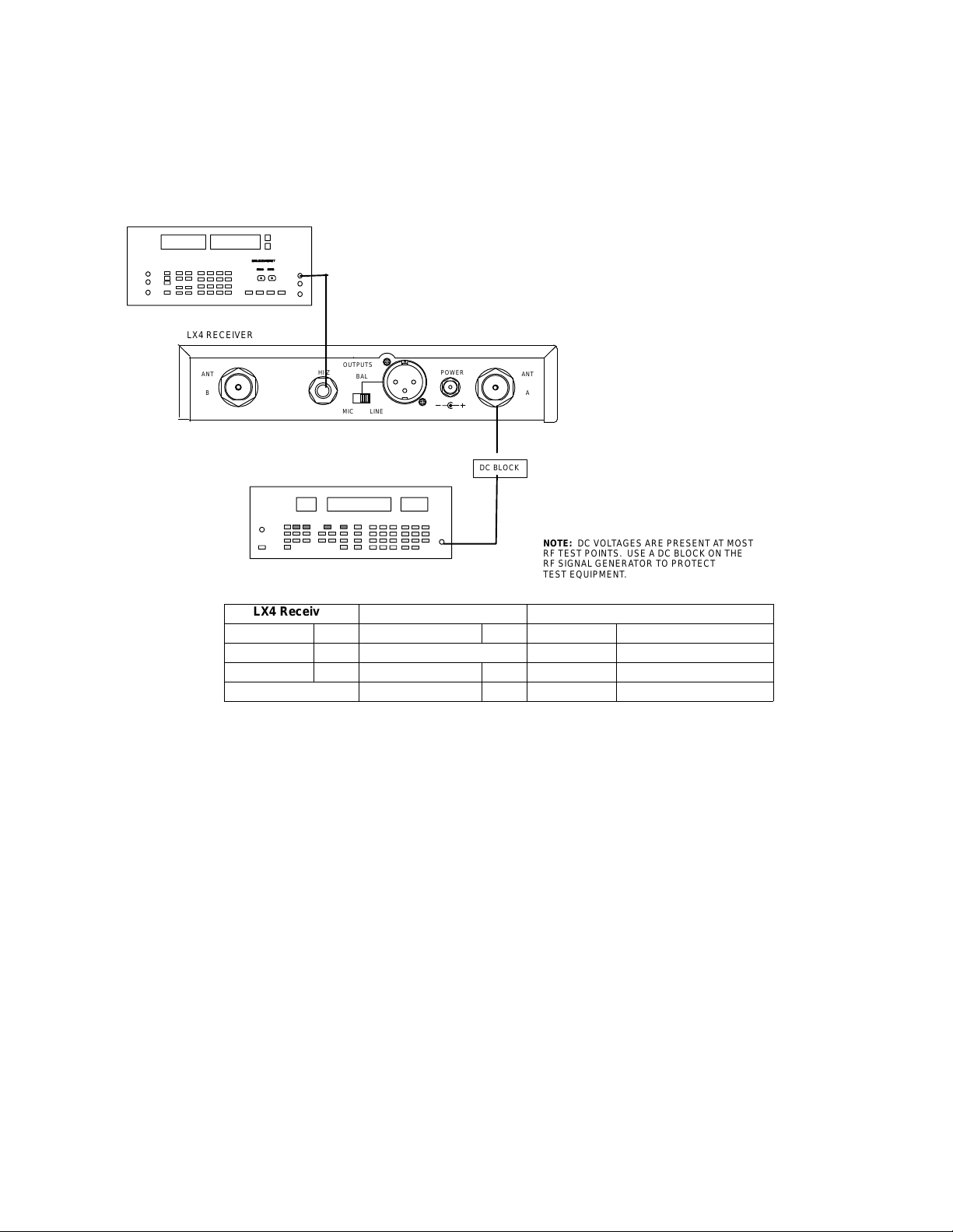
Check the Matching Receiver
AUDIO ANALYZER
LX4 RECEIVER
HI Z
OUTPUTS
BAL
MIC LINE
POWER
12.5 – 18.9 VDC
ANTANT
AB
RF SIGNAL GENERATOR
DC BLOCK
NOTE: DC VOLTAGES ARE PRESENT AT MOST
RF TEST POINTS. USE A DC BLOCK ON THE
RF SIGNAL GENERATOR TO PROTECT
TEST EQUIPMENT.
LX4 Receiver Audio Analyzer Rf Signal Generator
Power switch: ON Frequency: 1 kHz Amplitude: –20 dBm
Gain: Max Filters: Modulation:: 1 kHz
Squelch: Mid Low-Pass (30 kHz): ON Deviation: 15 kHz
High-Pass (400 Hz): ON Frequency: LX2 operating frequency
Figure 4. Matching Receiver Functional Test
1. Connect the matching receiver’s antenna input to the rf
signal generator. Set the rf signal generator’s amplitude to
–20 dBm, modulation to 1 kHz, deviation to 15 kHz, and set
the frequency to the LX2 unit’s operating frequency.
2. Connect the audio from the unbalanced output to the audio
analyzer with a 3.3 kΩ load. Turn the volume control to
maximum.
Preliminary Tests
3. Engage the audio analyzer’s 400 Hz high-pass filter and 30 kHz
low-pass filter..
4. For the LX4, verify the following:
S audio level is 400 mVrms ("90 mV)
S total harmonic distortion (THD) is < 0.75%
10
25D1006 (CG)
Page 12
ÁÁ
Á
Á
Á
ÁÁÁÁÁÁ
Á
Á
Á
Á
Á
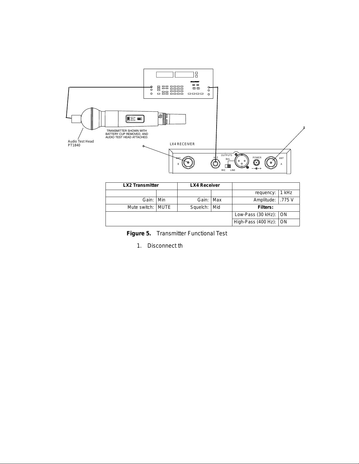
Audio Test Head
PT1840
Check the Transmitter
TRANSMITTER SHOWN WITH
BATTERY CUP REMOVED, AND
AUDIO TEST HEAD ATTACHED.
LX2 Transmitter LX4 Receiver Audio Analyzer
Power switch: PWR Power switch: ON Frequency: 1 kHz
Gain: Min Gain: Max Amplitude: .775 V
Mute switch: MUTE Squelch: Mid Filters:
AUDIO ANALYZER
LX4 RECEIVER
Shure LX2 Hand-Held Transmitter
HI Z
OUTPUTS
BAL
MIC LINE
POWER
12.5 – 18.9 VDC
Low-Pass (30 kHz): ON
High-Pass (400 Hz): ON
ANTANT
AB
Figure 5. Transmitter Functional Test
1. Disconnect the rf signal generator from the receiver and turn the
rf power off. Monitor the receiver’s unbalanced audio output with
a 3.3 kΩ load and the audio analyzer. Turn the receiver’s volume
control to its maximum setting.
2. Use an audio test head to input audio into the hand-held transmitter.
3. Turn the LX2 ON.
4. Inject a 0.775 V, 1 kHz signal from the audio analyzer into
the audio test head. Transmitter gain should be set to minimum.
Verify the following:
S the amplitude from the receiver’s unbalanced output equals
400 mVrms ("90 mV)
S total harmonic distortion (THD) is < 0.75%
5. Change the frequency of the audio generator to 100 Hz and
disengage the 400 Hz high-pass filter from the audio analyzer.
Verify that the audio level is –.5 dB ("0.5 dB) relative to the level
measured above.
6. Change the frequency of the audio generator to 10 kHz and
reengage the 400 Hz high-pass filter. Verify that the audio level,
relative to that measured above, is 0 dB, "2 dB.
25D1006 (CG)
Preliminary Tests11
Page 13
Shure LX2 Hand-Held Transmitter
Tested Units
If the system components pass the RF and Audio tests, then the sys-
tem is functioning correctly and does not require tuning and alignment.
Disassembly and Assembly
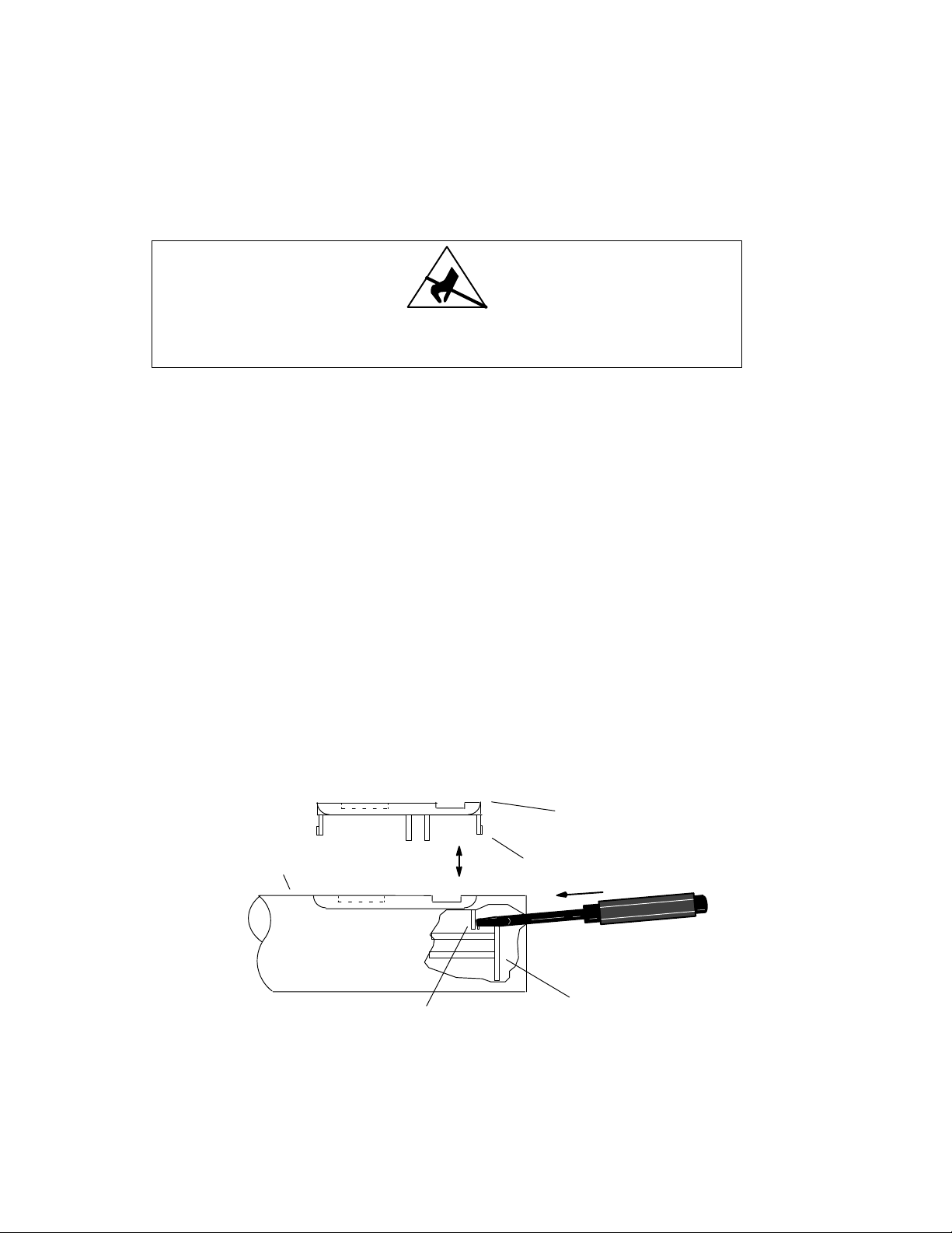
! CAUTION !
Observe precautions when handling this static-sensitive device.
Disassembly
To access the printed circuit boards of the unit, open the case:
1. Make sure the PWR/OFF switch is in the OFF position.
Handle
2. Unscrew the battery cup to access and remove the battery.
3. Unscrew the microphone cartridge and grille assembly.
4. If removal of the microphone-transmitter subassembly is necessary, use snap ring pliers to remove the retaining ring from inside
the microphone handle.
5. To remove the bezel, carefully insert a small screwdriver into the
microphone handle. Press against the plastic bezel tab and lift
upward. Remove the bezel, associated nameplate, and switch
actuators.
6. Remove the transmitter subassembly (audio, rf, and head circuit
board) from the handle while noting the internal guides they were
positioned on.
Bezel
Right side view of microphone
Tab
Preliminary Tests
Tab
Figure 6. Bezel Removal
12
Circuit board subassembly
25D1006 (CG)
Page 14
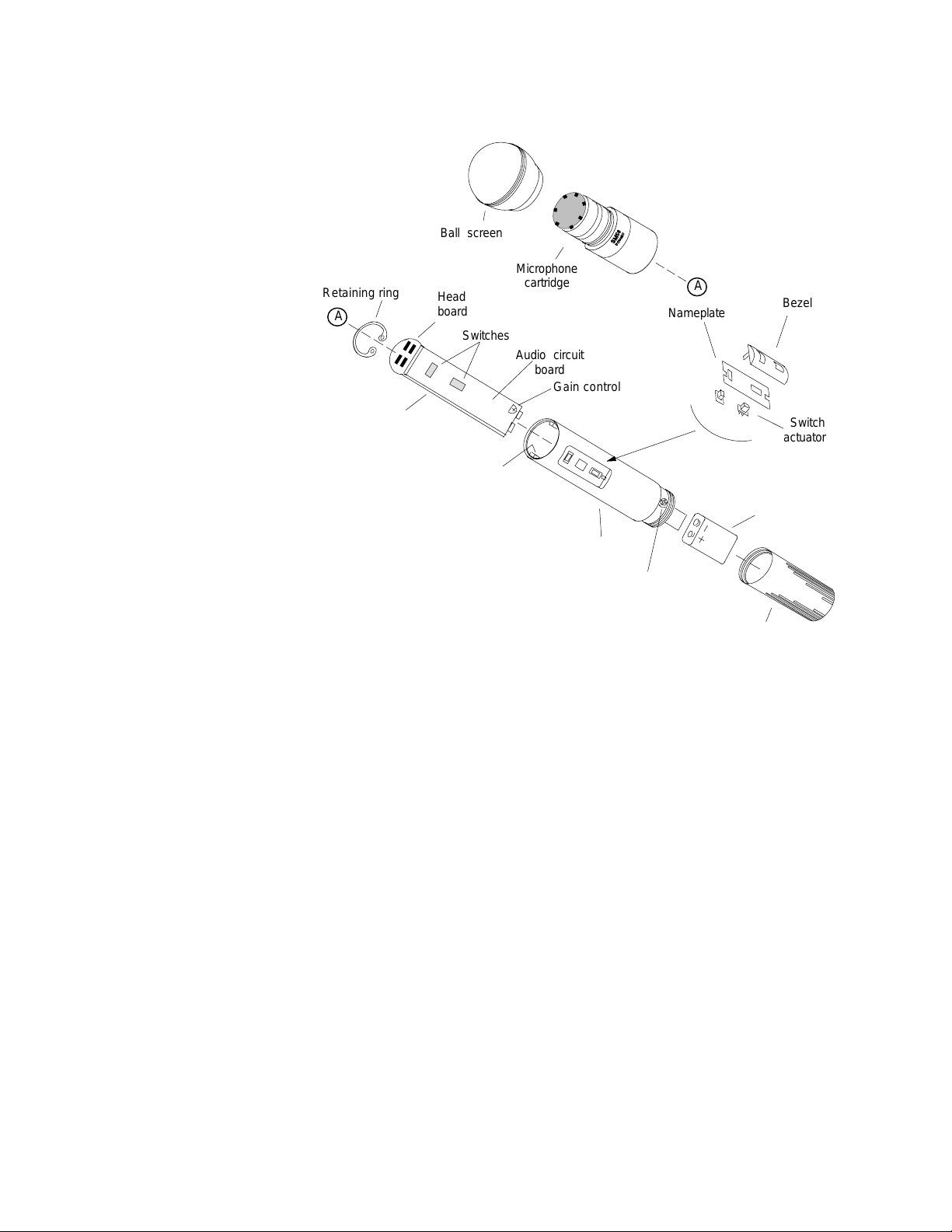
ÁÁ
ÁÁ
ÁÁÁ
Retaining ring
A
Ball screen
Head
board
Switches
Shure LX2 Hand-Held Transmitter
Microphone
cartridge
Audio circuit
board
Gain control
A
Nameplate
Bezel
Reassembly
Rf circuit
board
Circuit
board
guides
Handle
Gain control
access
Battery cup
Switch
actuators
9 V alkaline
battery
Figure 7. LX2 Hand-Held Transmitter, exploded view.
1. Make sure the PWR/OFF switch is in the OFF position.
2. Replace the transmitter subassembly (audio, rf, and head circuit
board) into the handle. Position it using the internal guides.
3. Carefully replace the nameplate, switch actuators, and bezel.
25D1006 (CG)
4. Replace the retaining ring.
5. Replace and screw in the microphone cartridge and
grille assembly.
6. Replace the battery.
7. Replace and screw in the battery cup.
Preliminary Tests13
Page 15

Shure LX2 Hand-Held Transmitter
Service Procedures
Measurement Reference
dBu is a measure of voltage, and dBm is a measure of power.
For example, the HP8903 should be labeled dBu instead of dBm
because it is a voltage measurement. These two terms are often used
interchangeably even though they have different meanings.
Audio levels in dBu are marked as dBm on the HP8903.
0 dBV = 2.2 dBu
0 dBu = 0 dBm, assuming the load = 600 Ω
Test Equipment
Most test equipment needed is described in the Shure Wireless
Service Equipment Manual. The following test equipment (or approved
equivalent) is also needed.
dB Conversion Chart
Equipment Type Model
Audio analyzer *Hewlett-Packard 8903B
Digital multimeter Fluke 87
Cable PT1843
Frequency counter Hewlett-Packard 53181A
Rf signal generator Hewlett-Packard 8656B
Spectrum analyzer Hewlett-Packard 8590L
Shure LX4 receiver Shure LX4
Audio test head adapter ring PT1838Y
Audio Test Head PT1840
*Audio levels in dBu are marked as dBm on the HP8903B.
Changing the Frequency
System Operating Frequencies
The LX2 Hand-Held Transmitter printed circuit board (pcb) is marked
with a group letter that identifies the range of frequencies it can operate
within.
Table 1
Test Equipment
Service Procedures
The operating frequency may be changed to a different frequency
within the same group. Before changing the operating frequency, refer
to the Functional Test section and check the transmitter for proper
operation.
14
25D1006 (CG)
Page 16

Shure LX2 Hand-Held Transmitter
Change the frequency by changing the crystal on the rf board.
For proper operation, the crystal must be obtained from Shure and must
operate within the frequency range of the pcb. Use the following equation to determine the operating frequency:
Carrier frequency = 9 x (nominal crystal frequency in MHz) – .09 MHz
After the new crystal is installed, operational tests and alignment procedures must be performed to ensure that the transmitter is operating
correctly . The pcb label should also be updated to show the new
frequency and letter identification code.
Table 2
Wireless Frequency Selections, Domestic (FCC/IC)
Group
Code
A
B
C
Frequency-
Code
V 169.445
AD 169.505
AC 170.245
AH 170.305
AB 171.045
AG 171.105
W 171.845
AA 171.905
AZ 174.500
CA 176.200
CC 177.600
CD 180.400
CE 182.200
CF 183.600
CG 186.200
CH 186.600
CJ 189.000
CK 190.600
CL 192.200
CM 192.600
CN 195.000
CP 196.600
CS 200.300
CQ 202.200
CR 203.000
CT 206.000
CV 208.200
CU 209.000
Frequency
(MHz)
Printed Circuit
Board Assembly
T90__8644
25D1006 (CG)
Service Procedures15
Page 17

Shure LX2 Hand-Held Transmitter
Wireless Frequency Selections, Euro (ETSI)
Group
Code
A
A
B
C
D
E
F
H
K
Table 3
Frequency
Code
AQ 173.800
EA 173.800
AY 174.100
EB 174.100
EC 174.500
ZZ 174.500
EE 175.000
J/BB 175.000
NB 175.000
NC 176.200
ND 176.600
K 177.000
NE 177.600
NH 182.000
NJ 183.200
NK 183.600
NL 184.600
S 184.800
NM 186.350
NP 189.000
NR 190.600
EG 191.900
NX 197.600
NY 198.600
EK 200.300
NZ 200.350
PU 201.650
PB 203.000
PC 204.200
PD 204.600
EH 208.300
EJ 216.100
PN 216.300
PP 217.000
PQ 218.200
PR 218.600
PS 219.600
PT 221.350
PV 232.825
PX 233.125
PY 234.625
PZ 237.325
Frequency
(MHz)
Printed Circuit
Board Assembly
T90__8704
Service Procedures
16
25D1006 (CG)
Page 18

Alignment
Shure LX2 Hand-Held Transmitter
AUDIO ANALYZER
NOTE: Whenever soldering is performed on the
curcuit boards, always power off the unit.
L209
Y201
R217
LX2 Transmitter Audio Analyzer
Power supply: 9 Vdc Filters:
Power switch: PWR 400 Hz High-Pass: ON
Mic switch: MUTE 30 kHz Low-Pass: ON
Gain: Mid
C217
RF BOARD (TOP)
C216
I210
I2GN
C240
Figure 8. Rf Alignment Test Set-Up (Domestic)
S The alignment procedure is sequential and does not change,
unless specified.
S Use RG58 or any other low-loss, 50 Ω test cables for all rf
connections.
S Keep the test cables as short as possible.
S Include the insertion loss of the cables and the connectors
for all rf measurements.
J101
+
–
J102
S Dc voltages are present at most rf test points. Use dc blocks
to protect the test equipment, if necessary.
1. Connect a 9 Vdc power supply to the battery terminals.
2. Make sure the mic ON/MUTE switch is in the MUTE position.
3. Set the audio gain potentiometer (R125) at mid-range.
4. Activate the 400 Hz high-pass and 30 kHz low-pass filters
on the audio analyzer.
25D1006 (CG)
Service Procedures17
Page 19

Shure LX2 Hand-Held Transmitter
Power and Display Check
LX2 Transmitter
Power supply: 9 Vdc
Power switch: PWR
Mic switch: MUTE
Gain: Mid
Figure 9. Power and Display Check Test Set-Up
1. Make sure the power OFF/PWR switch is in the PWR position.
2. With the 9.0 Vdc power supply connected, the green LED should
be illuminated.
3. Reduce the power supply to 6.6 Vdc. The yellow battery LED
should be illuminated.
4. Reduce the power supply to 6.0 Vdc. The red battery LED
should be illuminated.
5. Return the power supply to 9.0 Vdc.
6. Make sure the mic ON/MUTE switch is in the MUTE position.
7. Connect the positive (+) lead of a 9.0 Vdc power supply to the
positive battery terminal on the audio board. Connect the negative (–) lead to the battery terminal (audio board ground). The
green power LED should now be illuminated. If not, there is a
circuit malfunction.
8. Temporarily reverse the polarity of the 9.0 Vdc power supply.
The green power LED should be extinguished, and no current
should be drawn from the supply. Otherwise, there is a problem
with the reverse polarity protection circuit. Return the polarity of
the 9.0 Vdc power supply to normal.
Service Procedures
18
25D1006 (CG)
Page 20

Shure LX2 Hand-Held Transmitter
Ç
Ç
Ç
Rf Alignment: Domestic (FCC/IC)
During rf alignment, the transmitter output is terminated in a 50 Ω,
nonreactive load RG174 cable and monitored with a spectrum analyzer.
No modulation is applied during rf alignment.
SPECTRUM ANALYZER
L209
Y201
R217
RF BOARD (TOP)
I210
C217
C216
Power supply: 9 Vdc Center frequency: carrier
Power switch: PWR Span: 1 MHz
C240
I2GN
LX2 Transmitter Spectrum Analyzer
Mute switch: MUTE Reference level: + 20 dBm
J101
+
–
J102
Figure 10. Rf Alignment (FCC/IC)
1. Remove C240 on rf circuit board.
2. Tack-solder the 50 Ω test cable to side 1 of the rf circuit board:
S Connect the center conductor to the solder pad, I210.
S Connect the shield to I2GN (ground).
3. Connect the 50 Ω test cable to the spectrum analyzer.
FREQUENCY COUNTER
CH 2
CH 1
Scale: 10 dB/div
25D1006 (CG)
4. Peak C216 and C217 for maximum output power on the spectrum analyzer. Output should be 15 ± 2 dBm, including cable
losses. If the correct power cannot be attained, see the Bench
Checks section.
5. Connect the 50 Ω test cable to the frequency counter. Adjust
L209 to set the carrier frequency to within ± 1 kHz of designated
value. If correct frequency cannot be attained, see the Bench
Checks section.
6. Reconnect the 50 Ω test cable to the spectrum analyzer.
7. Confirm that the output power remained within specification.
If not, readjust C216 and C217.
Service Procedures19
Page 21

Shure LX2 Hand-Held Transmitter
Final Output Power / Frequency Calibration (Domestic)
This procedure correctly aligns the transmitter’s operating (output) frequency.
FREQUENCY COUNTER
SPECTRUM ANALYZER
J101
CH 2
CH 1
L209
LX2 Transmitter
Power supply: 9 Vdc Carrier frequency: carrier
Power switch: PWR Span: 1 MHz
Mute switch: MUTE Reference level: + 20 dBm
Gain: Mid Scale: 10 dB/div
L201
Y201
R217
C217
RF BOARD
SIDE 1
Y201
R201
C214
RF BOARD
Spectrum Analyzer
SIDE 2
C216
C216
C222
I210
I2GN
C240
J102
C226
Figure 11. Final Output Power / Frequency Calibration Test Set-Up
1. Connect the 50 Ω test cable to the frequency counter. With a
pink Toray driver, adjust L209 to set the rf carrier frequency to
within ±1 kHz of the operating frequency of the unit under test.
+
–
J101
+
–
J102
2. Reconnect the 50 Ω test cable to the spectrum analyzer. Peak
C226 for maximum output power on the spectrum analyzer.
3. Confirm that the output power is 15 dBm (±2 dBm).
Service Procedures
20
25D1006 (CG)
Page 22

Shure LX2 Hand-Held Transmitter
Spurious Emissions and Current Drain: Domestic
SPECTRUM ANALYZER
L209
R217
Y201
J101
C217
I210
C216
Power supply: 9 Vdc Scale: 10 dB/div
Power switch: ON Start frequency: 10 MHz
C240
I2GN
LX2 Transmitter
Mute switch: MUTE Stop frequency: 1 GHz
+
J102
RF BOARD
SIDE 1
–
Spectrum Analyzer
Reference level: 20 dBm
Figure 12. Spurious Emissions and Current Drain Test Set-Up
1. Set the spectrum analyzer as follows. Set the scale to 10 dB/div,
the start frequency to 10 MHz, the stop frequency to 1 GHz, and
the reference level to 20 dBm.
2. Check the level of spurious emissions. All spuri ous emissions
must be at least 30 dB below the carrier level. If necessary,
retune C216.
3. With a digital multimeter, measure the current drain of the
transmitter: it should be less than 35 mA. If it is too high, try
detuning C216, but make sure that the power and spurious
response remain within specification.
25D1006 (CG)
4. Check that 9 Vdc (±0.35 Vdc) is present at the head board
+9 V location (I133 on the audio board).
Service Procedures21
Page 23

Shure LX2 Hand-Held Transmitter
Rf Alignment: Euro (ETSI)
Do not apply modulation during the following rf alignment
procedures. If you cannot achieve any of the settings described
in this procedure, consult the Bench Checks section.
SPECTRUM ANALYZER
L201
Y201
R217
TP5
C222
C214
C216
RF BOARD (TOP)
ETSI
LX2 Transmitter Spectrum Analyzer
Power source: 9 Vdc Center frequency: 1/3 of the transmitter freq
Power switch: PWR Span: 30 MHz
Mute switch: MUTE Reference level: + 20 dBm
C226
Figure 13. Rf Alignment (Euro)
Note: See the Service Equipment Manual for conversion of a 50 Ω
BNC cable–to–RGU174 cable to a high impedance probe.
1. Tack-solder the high-impedance probe to the rf circuit board bottom:
S Connect the center conductor to TP5 (base of Q202).
S Connect the shield to circuit ground.
2. Carefully remove C242 from the rf board. This disconnects
the battery (antenna) to allow accurate conductive-power
measurements.
TP6
TP7
J201
+
–
J202
Scale: 10 dB/div
Service Procedures
3. Connect the high-impedance probe to the spectrum analyzer.
4. Verify that the mic switch is in the MUTE position.
5. On the spectrum analyzer, set the center frequency to one-third
the frequency of the transmitter. Set the span to 30 MHz, the
reference level to +20 dBm, and the scale to 10 dB/div.
22
25D1006 (CG)
Page 24

FREQUENCY COUNTER
SPECTRUM ANALYZER
Shure LX2 Hand-Held Transmitter
Final Output Power / Frequency Calibration (Euro)
CH 2
CH 1
L201
Y201
R217
LX2 Transmitter Spectrum Analyzer
Power source: 9 Vdc Center frequency: 1/3 of the transmitter freq
Power switch: PWR Span: 30 MHz
Mute switch: MUTE Reference level: + 20 dBm
Scale: 10 dB/div
TP5
C222
C214
C216
RF BOARD (TOP)
ETSI
C226
TP6
TP7
J201
+
–
J202
Figure 14. Final Output Power / Frequency Calibration Test Set-Up
Note: See the Service Equipment Manual for conversion of a 50 Ω
BNC cable–to–RGU174 cable to a high impedance probe.
1. With a yellow Toray non-conductive screwdriver, adjust C214 for
maximum (peak) output power on the spectrum analyzer. For
better resolution while tuning, switch the scale to 2 dB/div and
adjust the reference level to the center of the screen.
2. Remove the high-impedance probe. Connect the standard 50 Ω
test cable to TP6 (before antenna-matching).
3. Connect the BNC end of the cable to the spectrum analyzer.
4. Set the center frequency to the frequency of the transmitter.
5. Adjust C216 and C222 for maximum (peak) output power on the
spectrum analyzer.
Note: C216 is not tunable on earlier ETSI-approved units.
6. Connect the 50 Ω test cable to the frequency counter. With a
pink Toray driver, adjust L201 to set the RF carrier frequency to
within ±1 KHz of the operating frequency UNDER test.
25D1006 (CG)
7. Reconnect the 50 Ω test cable to the spectrum analyzer. Peak
C226 for maximum output power on the spectrum analyzer.
8. Confirm that the output power is 9.5 dBm (±2 dBm).
Service Procedures23
Page 25

Shure LX2 Hand-Held Transmitter
Spurious Emissions and Current Drain: Euro
L201
Y201
SPECTRUM ANALYZER
C214
R217
C216
RF BOARD (TOP)
ETSI
C222
C226
+
J201
–
J202
TP1
4TP
TP3
5
TP2
J201
+
–
J202
LX2 Transmitter
Power supply: 9 Vdc Scale: 10 dB/div
Power switch: PWR Start frequency: 10 MHz
Mute switch: MUTE Stop frequency: 1 GHz
TP6
TP8
TP7
TP9
RF BOARD (BOTTOM)
Reference level: 20 dBm
TP5
ETSI
Spectrum Analyzer
Figure 15. Spurious Emissions and Current Drain Test Set-Up
1. Set the spectrum analyzer as follows. Set the scale to 10 dB/div,
the start frequency to 10 MHz, the stop frequency to 1 GHz, and
the reference level to 20 dBm.
2. Check the level of spurious emissions. All spuri ous emissions
must be at least 44 dB below the carrier level. If necessary,
retune C226.
Service Procedures
3. With a digital multimeter, measure the current drain of the
transmitter: it should be less than 35 mA. If it is too high, try
detuning C226, but make sure that the power and spurious
response remain within specification.
4. Check that 9 Vdc (±0.35 Vdc) is present at the head board
+9 V location (I133 on the audio board).
24
25D1006 (CG)
Page 26

Shure LX2 Hand-Held Transmitter
ÁÁÁÁÁÁ
Á
Á
Á
Audio Alignment: Domestic and Euro
AUDIO ANALYZER
S101
R130
S102
AUDIO BOARD
(TOP)
C107
U101
R125
U102
J102
–
+
J101
TRANSMITTER SHOWN WITH
BATTERY CUP REMOVED, AND
AUDIO TEST HEAD ATTACHED.
Power supply: 9 Vdc Frequency: 1 kHz
Power switch: PWR Amplitude: 230 mV
Figure 16. Audio Alignment Test Set-Up
1. Put the mic (mute) switch in the ON position.
2. Turn the LX2 power OFF.
3. Replace C240 for domestic, C242 for Euro, on the rf pcb.
4. Use a soldering iron to remove the 50 Ω test cable.
5. Turn the LX2 power ON.
6. Ins ert the pcb assembly through the brass ring and
LX2 Transmitter Audio Analyzer
Mic switch: ON Filters:
Gain: Mid 400 Hz High-Pass: ON
30 kHz Low-Pass: ON
screw on the audio test head.
25D1006 (CG)
7. Set the audio analyzer output to a frequency of 1 kHz and an
amplitude of 230 mV.
8. Connect the output of the audio analyzer to the
audio test head.
9. Adjust R125 (gain) for 775 ± 0 mV (0.775 V) or 0 dBu ± .1 dBu
at the anode (+) side of C107 on the audio board.
Service Procedures25
Page 27

Shure LX2 Hand-Held Transmitter
ÁÁ
Á
Á
Á
Deviation Reference Voltage (Domestic and Euro)
AUDIO ANALYZER
LX4 RECEIVER
RF SIGNAL GENERATOR
HI Z
OUTPUTS
BAL
MIC LINE
POWER
12.5 – 18.9 VDC
DC BLOCK
ANTANT
AB
NOTE: DC VOLTAGES ARE PRESENT AT MOST
RF TEST POINTS. USE A DC BLOCK ON THE
RF SIGNAL GENERATOR TO PROTECT
TEST EQUIPMENT.
LX2 Transmitter LX4 Receiver Audio Analyzer Rf Signal Generator
Power switch: OFF Power switch: ON Frequency: 1 kHz Frequency: carrier
Mute switch: ON Gain: Max Filters: Modulation: FM
Squelch: Mid Low-Pass (30 kHz): ON Modulation source: 1 kHz
High-Pass (400 Hz): ON Output amplitude: –38 dBm
Figure 17. Deviation Reference Voltage Test Set-Up
1. Turn the LX2 power OFF.
2. Set the rf signal generator with the frequency the same as the
carrier, modulation at FM, modulation source at INT 1 kHz, the
FM deviation at ± 15 kHz, and the amplitude at –38 dBm.
3. Connect the output of the rf signal generator to either antenna
input of a receiver. Use a receiver that is the same frequency as
the LX2, such as the LX3 or LX4 that came with the LX2.
4. Set the volume control on the front panel of the receiver to the
maximum position (full clockwise rotation) and apply power to
the receiver. Set the squelch control of the receiver at midrange.
5. Measure the rms voltage developed across the Hi-Z output,
terminated in 3.3 kΩ, of the receiver. The measured rms voltage
should be approximately 0.389 V rms. This is the audio output
voltage that corresponds to a deviation level of 15 kHz.
Record this voltage as the Deviation Reference Voltage.
Service Procedures
6. Turn off the rf output on the rf signal generator.
26
25D1006 (CG)
Page 28

Shure LX2 Hand-Held Transmitter
ÁÁ
Á
Á
Á
ÁÁÁÁÁÁ
Á
Á
Á
Deviation Adjustment (Domestic and Euro)
L209
L201
TRANSMITTER SHOWN WITH
BATTERY CUP REMOVED, AND
AUDIO TEST HEAD ATTACHED.
Y201
R217
C217
RF BOARD (TOP)
DOMESTIC
Y201
C214
R217
RF BOARD (TOP)
C216
ETSI
C216
C222
I210
I2GN
C240
C226
J101
+
–
J102
+
J201
–
J202
AUDIO ANALYZER
LX4 RECEIVER
S101
R130
HI Z
S102
OUTPUTS
BAL
MIC LINE
C107
U101
R125
U102
POWER
12.5 – 18.9 VDC
ANTANT
LX2 Transmitter LX4 Receiver Audio Analyzer Rf Signal Generator
Power supply: 9 Vdc Power switch: ON Frequency: 1 kHz Frequency: carrier
Power switch: PWR Gain: Max Filters: Modulation: FM
Mute switch: ON Squelch: Mid Low-Pass (30 kHz): ON Modulation source: 1 kHz
High-Pass (400 Hz): ON Rf output: OFF
–
+
AB
Figure 18. Deviation Adjustment Test Set-Up
1. Make sure the rf output on the rf signal generator is turned OFF.
2. Connect the output of the audio analyzer to the test head.
3. Turn the LX2 power ON.
4. Set the frequency of the audio analyzer to 1 kHz. Make sure that
the level at the anode (+) of C107 is still 0.775 V ± 50 mV.
5. Disconnect any cables from the antenna inputs of the receiver
and place an antenna on the receiver.
6. Measure the rms voltage at the unbalanced Hi-Z output of
the receiver. Adjust R217 (domestic) or R201 (Euro) to 0 ± 1 dB
relative to the deviation reference voltage measured above as
the Deviation Reference Voltage. The deviation reference
voltage was established earlier using the calibrated rf signal
generator.
25D1006 (CG)
Service Procedures27
Page 29

Shure LX2 Hand-Held Transmitter
ÁÁ
Á
Á
Á
ÁÁÁÁÁÁ
Á
Á
Á
Distortion Adjustment (Domestic and Euro)
TRANSMITTER SHOWN WITH
BATTERY CUP REMOVED, AND
AUDIO TEST HEAD ATTACHED.
Power supply: 9 Vdc Power switch: ON Frequency: 1 kHz
Power switch: PWR Gain: Max Filters:
S101
R130
S102
C107
U101
R125
U102
AUDIO ANALYZER
LX4 RECEIVER
HI Z
OUTPUTS
BAL
MIC LINE
POWER
12.5 – 18.9 VDC
LX2 Transmitter LX4 Receiver Audio Analyzer
Mute switch: MUTE Squelch: Mid Low-Pass (30 kHz): ON
High-Pass (400 Hz): ON
–
+
ANTANT
AB
Figure 19. Deviation Adjustment Test Set-Up
1. Set the audio analyzer for DISTN (distortion, THD).
2. Adjust R130 for minimum distortion out of the receiver.
System distortion should be less than 1%.
Service Procedures
28
25D1006 (CG)
Page 30

AUDIO ANALYZER
Shure LX2 Hand-Held Transmitter
Audio Frequency Response (Domestic and Euro)
C107
S101
LX2 Transmitter Audio Analyzer
Power supply: 9 Vdc Frequency: 100 Hz
Power switch (S101): PWR Amplitude: 230 mV
Mic switch (S102): ON Filters:
S102
U101
R130
400 Hz High-Pass: OFF
30 kHz Low-Pass: ON
R125
U102
–
+
Figure 20. Frequency Response Test Set-Up
Note: Press the LOG/LIN button on the audio analyzer to measure in
dB. Then press the RATIO button to perform the relative measurement
in the next section.
1. Remove the 400 Hz high pass filter from the audio analyzer.
2. Change the frequency of the audio analyzer to 100 Hz.
3. Verify that the audio level is equal to –0.5 ± 0.5 dB
relative to the level measured at the anode (+) of C107 at 1 KHz.
25D1006 (CG)
4. Activate the 400 Hz high-pass filter on the audio analyzer.
5. Change the frequency of the audio analyzer to 10 kHz. Verify
that the audio level is equal to +3.0 ± 0.5 dB relative to the
level measured at the anode (+) of C107 at 1 KHz.
6. Turn the LX2 power OFF.
Service Procedures29
Page 31

Shure LX2 Hand-Held Transmitter
Bench Checks
Power Input Problem
Dc Input
n Verify that 9.0 Vdc ± 0.35 Vdc is present at the 9.0 Vdc test
point (U101, pin 13). If this voltage is low, check N33.
n Check the power switch bias on Q105 and L101.
n Make sure the circuit board ground is 0.0 Vdc.
n If there is a short from 9.0 Vdc to ground, try to isolate different
parts of the circuit; narrow it down to the rf or audio section.
n Look for foil shorts, solder bridges, and capacitors that have
been installed backwards.
n Check for 5.0 Vdc ± 0.25 Vdc at N147. If voltage is low, check
the +5.0 Vdc test point (U101, pin 7). If the voltage is not correct, check U101, pin 13 for 9.0 Vdc; also check the values of
R133, R135, and R137.
n If dc voltages are being measured at points that have rf present,
use a 10 kΩ resistor at the probe to prevent loading the circuit.
Excessive Current Drain
Domestic (FCC/IC)
n Readjust C216 for lower current drain while maintaining output
power to specification.
n If current drain is still excessive, there may be a short, wrong
resistor values, or a defective capacitor.
n Make sure that R219 is the correct value for the frequency group.
n Last of all, try changing Q204.
Euro (ETSI)
n Readjust C226 for lower current drain while maintaining output
power to specification.
n If current drain is still excessive, there may be a short, wrong
resistor values, or a defective capacitor.
n Make sure that R218 is the correct value for the frequency group.
n Last of all, try changing Q204.
Bench Checks
30
25D1006 (CG)
Page 32

Audio
Loss
Shure LX2 Hand-Held Transmitter
n Make sure mic switch is ON.
n Determine where the signal is being lost. Verify audio at U102,
pin 7. Then check dc bias at U102, pins 5, 6, and 7. They
should be about half of the supply voltage, or around 4.5 Vdc.
This bias comes from the 9.0 Vdc line through voltage divider
R103/R105, then through R106 to pin 5.
n Look for open vias, foil shorts, incorrect parts, and bad connec-
tions.
n If there is audio at pin 7, but not at pin 14, check again for db
bias.
n Pins 12 and 13 should read approximately 1.8 Vdc, while pin 14
should read about 3.7 Vdc. Dc bias comes from U101, pin 9,
through R107 to U102, pin 12.
n Next, check parts in the feedback path from pin 14 to pin 13,
parts connected to pin 7, and connections from U102 to U101.
Also check the connections from U102, pin 14, to the next stage
and to the limiter (Q103), and U101, pin 15.
n The last stage is to check U102, pins 8, 9, and 10. Dc bias
should be about 4.0 Vdc for all three pins. Dc bias comes from
the 5.0 Vdc line through R104 to U102, pin 10. Check values in
feedback from pin 8 to pin 9, and the path to Q104 and Q101,
pin 16.
Distortion
n Make sure the analyzer’s 400 Hz high pass and 30 kHz low pass
filters are in. U101, pin 9, should read about 1.8 Vdc.
n The dc level on the wiper of R130 should change from about 1.5
Vdc to 3.5 Vdc when you turn R130. If not, check, R129, C125,
R141, R140, R126, and the parts tied to U101, pin 9. Make sure
the audio level is correct.
n Last of all, try replacing D201 and Y201.
25D1006 (CG)
Bench Checks31
Page 33

Shure LX2 Hand-Held Transmitter
RF Problems: Deviation
Domestic (FCC/IC)
n There must be a good carrier to get any deviation.
n If R217 cannot be adjusted to obtain 15 kHz deviation, try to iso-
late the problem to the audio or rf section. Check for –2.2 dBv at
I118; if not, refer to the Audio section of the circuit description.
n If the level is correct at I118, check R217, C220, C227, R208,
R216, D201, L209, and C214. The value of C214 is critical to
the deviation sensitivity.
n Last of all, try replacing D201 and Y201.
Euro (ETSI)
n There must be a good carrier to get any deviation.
n If R201 cannot be adjusted to obtain 15 kHz deviation, try to iso-
late the problem to the audio or rf section. Check for –2.2 dBv at
I118; if not, refer to the Audio section of the circuit description.
n If the level is correct at I118, check R201, C201, C202, R202,
R203, D201, L201, and C203. The cathode of D201 should be
getting 5.0 Vdc bias from the 5.0 Vdc line through R202 and
R203. The value of C203 is critical to the deviation sensitivity.
n Last of all, try replacing D201 and Y201.
Low Output Power
Domestic (FCC/IC)
n The output of the transmitter should be terminated in a 50 Ω load
n Probe the output after the oscillator stage (I230). If there is
n Make sure that when C217 is rotated 360 degrees, two separate
n Repeat the procedure for the second rf stage. C216 should also
n Repeat the procedure for the last rf power amp stage. Check the
from I210 to ground during testing. If the unit is being tested as
a two board assembly with the rf and audio boards soldered
together, temporarily remove C240 to disconnect the battery
antenna. The rf levels shown on the schematic were measured
with a FET probe without an rf ground and are only approximate.
none, refer back to the “Distortion” section.
peaks in the carrier output amplitude are produced. If there is
only one peak, make sure the C217 is the correct color (value).
Check values of L205, C225, C234, L202, C233; and check bias
on Q201. Last of all, replace Q201.
be turned one complete rotation to check for two peaks in the
output power. If only one peak is observed, make sure that
C216 is the correct color (value). Check values of L204, C238,
C236, L210, C235, C222, C226; and check bias on Q203. Last
of all, replace Q203.
dc bias on Q204 and values of all parts from the base of Q204 to
I210. Last of all, replace Q204.
Bench Checks
32
25D1006 (CG)
Page 34

Euro (ETSI)
Shure LX2 Hand-Held Transmitter
n If the power is slightly low and the spurious level is high, check
for wrong or open coils at L202, L210, and L206.
Note: In addition to the frequency determining components discussed
above, bypass capacitors can affect the tuning and power gain of rf
stages. Emitter bypass capacitors C226 and C223 can be probed with
the FET probe. If the rf level measured on each side of the part is not
comparable, a defective capacitor is indicated. The bypasses on the
collector circuits C207 and C208 can be checked in the same way.
n The output of the transmitter should be terminated in a 50 Ω load
from TP6 to ground during testing. If the unit is being tested as a
two board assembly with the rf and audio boards soldered
together, temporarily remove C242 to disconnect the battery
antenna.
n Probe the output after the oscillator stage (TP5). If there is none,
refer back to the “Distortion” section.
n Make sure that when C214 is rotated 360 degrees, two separate
peaks in the carrier output amplitude are produced. If there is
only one peak, make sure the C214 is the correct value. Check
values of L202, C208, C244, C210, L203, C213, and C215; and
check bias on Q201. Last of all, replace Q201.
n Repeat the procedure for the next rf stage. C222 should also be
turned one complete rotation to check for two peaks in the output
power. If only one peak is observed, make sure that C222 is the
correct value. Check values of L204, C216, C245, C219, L205,
C221, and C224; and check bias on Q202. Last of all, replace
Q202.
n Repeat the procedure for the third rf stage. C226 should also be
turned one complete rotation to check for two peaks in the output
power. If only one peak is observed, make sure that C226 is the
correct value. Check values of L206, C227, C229, L207, C230,
and C232; and check bias on Q203. Last of all, replace Q203.
n Repeat the procedure for the last rf power amp stage. Check the
dc bias on Q204 and values of all parts from the base of Q204 to
TP6. Last of all, replace Q204.
n If the power is slightly low and the spurious level is high, check
for wrong or open coils at L205, L207, and L210.
Note: In addition to the frequency determining components discussed
above, bypass capacitors can affect the tuning and power gain of rf
stages. Collector bypass capacitors C220 C227, and C234 can be
probed with the FET probe. If the rf level measured on each side of the
part is not comparable, a defective capacitor is indicated. The bypasses
on the collector of Q203 (C228) can be checked in the same way. Also,
the rf level measured with the FET probe should drop approximately 10
dB from the collector of one transistor to the base of the next transistor.
If the drop is higher than 12 dB, thoroughly check the stage with the
excessive loss in power.
25D1006 (CG)
Bench Checks33
Page 35

Shure LX2 Hand-Held Transmitter
Notes:
Notes:
34
25D1006 (CG)
Page 36

Shure LX2 Hand-Held Transmitter
Replacement Parts and Drawings
Parts Designations
The following comments apply to the parts list and the schematic:
Resistors: Unless otherwise noted, all resistors are surface-
mount with 1/10 W rating and 1% tolerance.
Capacitors: Unless otherwise noted, non-polarized capacitors
are surface-mount NPO dielectric types with a 100 V capacity and a
5% tolerance, and polarized capacitors are tantalum types.
Table 4
Replacement Parts
Reference
Designation
A1 Programmed circuit board assembly (Domestic)
A2 Programmed circuit board assembly (Euro)
MP1 Battery cup (painted) 65A8241A
MP2 Battery snap (negative) 56A318
MP3 Battery snap (positive) 56A317
MP4 Bezel *** OLD Version *** 65A8242 not available
MP5 Compression disc 38A180
MP6 Contact (head board) 53F2039A
MP7 Handle *** OLD Version *** 65A8220A not available
MP8
MP9 Bezel *current oval type* 65C8299
MP10 Actuator *current oval type* 65C8298
MP11 Retaining metal clip ring 30A1314
MP12
MP13 Actuator *old type* 65A8225
Y1 Crystal
Handle Current type. Uses oval Bezel and
Actuators. *** Must replace Actuators and Bezel if
replacing from Old version Handle ***
Kit contains: (2)Current type Actuators, clip ring
and (3)gold mic contacts
Description Shure Part Number
T90_8644 [See Table 9, p.
36, to determine the
group-letter in the underlined
space. e.g. T90CA8644].
T90–8704 [See Table 9, p.
36, to determine the
group-letter in the underlined
space. e.g. T90NX8704].
65C8427A
RPW614
40_8006A [See Table 2, p.
15 (Domestic) or Table 3, p.
16 (Euro) to determine the
crystal code in the underlined
space. e.g. 40NH8006A]
25D1006 (CG)
Replacement Parts and Drawings35
Page 37

Shure LX2 Hand-Held Transmitter
Audio Board Components: Side 1
Table 5
Reference Designation Description
S101, 102 Switch 55A178
D101 LED, red 184A18
D102 LED, amber 184B18
D103 LED, green 184D18
R125 Potentiometer 20 k 46B8049
R130 Potentiometer 20 k 146F02
Q106, 107, 108, 109, 110 Transistor 183A38
Q103, 104 Transistor 183A01
Q105 Transistor 183A07
Q201, 203, 204 Transistor 183A03
U101 Compander 188A01
U102 Opamp 188A49
Shure Part
Number
Table 6
Rf Board Components:
DOMESTIC (FCC/IC)
Reference Designation Description
C216 Trim cap. 3 – 10 pF / 100 V 152C02
L209 Coil, rf * 82–8015
R217 Potentiometer 25% 10 k 146E02
C217 Trim cap. 8.5–40 pF / 100 V 152F02
Shure Part
Number
*See Frequency Dependent Table.
Reference Designation Description
Group A
L209 Coil, rf 82A8015
Group B
L209 Coil, rf 82B8015
Group C
L209 Coil, rf 82C8015
Replacement Parts and Drawings
Table 7
Frequency Dependent Tables
Rf Board Components:
DOMESTIC (FCC/IC)
36
Shure Part
Number
25D1006 (CG)
Page 38

Shure LX2 Hand-Held Transmitter
Table 8
Rf Board Components:
EURO (ETSI)
Reference Designation Description
Shure Part
Number
R201 Potentiometer 1% 10 k 146E02
Table 9
Frequency Dependent Tables
Rf Board Components:
EURO (ETSI)
Group Frequency Range C208 C244 C210 C213 C215
A 169.000–174.000 MHz 15 pF –– 1.0 pF 33 pF 100 pF
B 174.000–181.000 MHz 12 pF 1.0 pF 1.0 pF 33 pF 100 pF
C 181.000–188.000 MHz 12 pF –– 1.0 pF 27 pF 100 pF
D 188.000–195.000 MHz 12 pF –– 1.0 pF 22 pF 100 pF
E 195.000–202.000 MHz 10 pF 0.5 pF 0.5 pF 22 pF 100 pF
F 202.000–209.000 MHz 8.2 pF 1.0 pF 1.0 pF 22 pF 100 pF
G 209.000–216.000 MHz 6.8 pF 1.5 pF 0.5 pF 18 pF 82 pF
H 216.000–223.000 MHz 6.8 pF 1.0 pF 0.5 pF 18 pF 82 pF
K 230.000–240.000 MHz 6.8 pF –– 0.5 pF 15 pF 82 pF
Group C245 C221 C224 C227 C230 C232 C234 C239 C241 C242
A 8.2 pF 33 pF 100 pF 4.7 pF 27 pF 27 pF 15 pF 27 pF 22 pF 12 pF
B 6.8 pF 33 pF 100 pF 4.7 pF 18 pF 27 pF 22 pF 22 pF 33 pF 8.2 pF
C 6.8 pF 27 pF 100 pF 4.7 pF 15 pF 27 pF 22 pF 18 pF 33 pF 6.8 pF
D 5.6 pF 22 pF 100 pF –– 15 pF 22 pF 18 pF 15 pF 6.8 pF 3.3 pF
E 5.6 pF 22 pF 100 pF –– 12 pF 22 pF 8.2 pF 15 pF 10 pF 6.8 pF
F 3.3 pF 22 pF 100 pF –– 12 pF 22 pF 27 pF 18 pF 18 pF 5.6 pF
G 3.3 pF 18 pF 82 pF –– 12 pF 18 pF 15 pF 18 pF 18 pF 4.7 pF
H 1.0 pF 18 pF 82 pF –– 12 pF 18 pF 15 pF 15 pF 15 pF 4.7 pF
K –– 15 pF 82 pF –– 10 pF 15 pF 15 pF 12 pF 12 pF 3.3 pF
25D1006 (CG)
Group R226 L206 L209 L211
A 750 Ω .056 uH .150 uH .220 uH 82A8015 R250
B 1000 Ω .056 uH .150 uH .220 uH 82A8015 R251
C 1000 Ω .056 uH .150 uH .220 uH 82A8015 R252
D 1210 Ω .056 uH .150 uH .220 uH 82B8015 R253
E 1000 Ω .056 uH .150 uH .180 uH 82B8015 R254
F 1330 Ω .056 uH .100 uH .180 uH 82B8015 R255
G 1330 Ω .047 uH .100 uH .180 uH 82C8015 R256
H 1000 Ω .047 uH .100 uH .180 uH 82C8015 R257
K 1000 Ω .047 uH .100 uH .180 uH 82C8015 R256 &
L201
Part # Group
Replacement Parts and Drawings37
R257
Page 39

Shure LX2 Hand-Held Transmitter
LX2 Hand-Held Transmitter
Head Board
DOMESTIC and EURO
I145
I140
J102
J101
I118
Side 1
I109
I108
I147
I104
I133
Side 2
LX2 Hand-Held Transmitter
Audio Board
DOMESTIC (FCC/IC approved)
38
Page 40

Side 1
Shure LX2 Hand-Held Transmitter
I209
I210
I201
I202
I218
Side 2
LX2 Hand-Held Transmitter
Rf Board:
Domestic
(FCC/IC approved)
39
Page 41

Shure LX2 Hand-Held Transmitter
Audio Board, Side 1
Audio Board, Side 2
Euro (ETSI)
Euro (ETSI)
I102
LX2 Hand-Held Transmitter
Euro (ETSI)
Printed Circuit Boards
40
Page 42

Shure LX2 Hand-Held Transmitter
Euro (ETSI)
RF Board, Side 1
Euro (ETSI)
RF Board, Side 2
LX2 Hand-Held Transmitter
Euro (ETSI)
Printed Circuit Boards
41
Page 43

Shure LX2 Hand-Held Transmitter
LX2 Hand-Held Transmitter:
Rf Schematic Diagram
EURO (ETSI approved)
Printed in U.S.A.
Page 44

Shure LX2 Hand-Held Transmitter
LX2 Hand Held Transmitter
Audio Schematic Diagram
DOMESTIC and EURO
Page 45

Shure LX2 Hand-Held Transmitter
LX2 Hand-Held Transmitter:
Rf Schematic Diagram
DOMESTIC (FCC/IC approved)
Printed in U.S.A.
 Loading...