

Page 1
Global LCD Panel Exchange Center
www.panelook.com
One step solution for LCD / PDP / OLED panel application: Datasheet, inventory and accessory!
www.panelook.com
PRODUCT SPECIFICATIONS
Liquid Crystal Displays Group
YS-150MS01
TFT-LCD Module
SHARP IN SIDE
Spec. Issue Date: Feb. 14, 2006
No: LD-150N2A
RECORDS OF REVISION
Page 2
Global LCD Panel Exchange Center
www.panelook.com
One step solution for LCD / PDP / OLED panel application: Datasheet, inventory and accessory!
www.panelook.com
SPEC No. DATE REVISED
PAGE SUMMARY NOTE
No.
1. Application
This specification applies to the color 15.0 XGA TFT-LCD module YS-150MS01.
Page 3
Global LCD Panel Exchange Center
www.panelook.com
One step solution for LCD / PDP / OLED panel application: Datasheet, inventory and accessory!
www.panelook.com
◎This 15.0 XGA TFT-LCD module specification are the proprietary product of SHARP
CO
RPORATION and Backlight module made by. Do not reproduce or cause any third party to
reproduce them in any form or by any means, electronic or mechanical, for any purpose, in whole or in
part, without the express written permission of SHARP.
◎The device listed in this technical literature was designed and manufactured for use in OA equipment.
◎In case of using the device for applications such as control and safety equipment for transportation
(aircraft, trains, autom
which require higher reliability and safety, take into consideration that appropriate measures such as
fail-safe functions and redundant system design should be taken.
◎Do not use the device for equipment that requires an extrem
applications, telecommunication equipment(trunk lines), nuclear power control equipment and medical
or other equipment for life support.
◎We assumes no responsibility for any damage resulting from the use of the device which does not
com
ply with the instructions and the precautions specified in these specification sheets.
2. Overview
This module is a color active matrix LCD module incorporating am
Transistor). It is composed of a color TFT-LCD panel, driver ICs, control circuit, power supply circuit and
a back light unit. Graphics and texts can be displayed on a 1024×RGB×768 dots panel with about 16
obiles, etc. ), rescue and security equipment and various safety related equipment
e level of reliability, such as aerospace
orphous silicon TFT (Thin Film
million colors by using LVDS (Low Voltage Differential Signaling) and supplying +3.3V DC supply
voltages for TFT-LCD panel driving and supply voltage for backlight.
3. Mechanical Specifications
Page 4
Global LCD Panel Exchange Center
www.panelook.com
One step solution for LCD / PDP / OLED panel application: Datasheet, inventory and accessory!
www.panelook.com
Parameter Specifications Unit
Display size
Active area 304.1 (H) 228.1 (V) mm
Pixel format
Pixel pitch 0.297 (H) 0.297 (V) mm
Pixel configuration R, G, B vertical stripe Display mode Normally white Brightness 350 (Typ) cd/m2
Respons time Tr=5 ,Td=20 ms
Contrast ration 350 : 1 View angle 55,80,80 Deg.
Unit outline dimensions *1 326.0(W) 252.0(H) 10.55(D) mm
Mass 1400 (MAX) g
Surface treatment Anti-glare and hard-coating 2H
38 (Diagonal) cm
15.0 (Diagonal) Inch
1024 (H) ×768 (V)
(1 pixel R+G+B dots) -
(Haze value = 28)
Pixel
*1. Note: excluding back light cables, cover and pet sheet.
The thickness of module (D) doesn’t contain the projection.
Outline dimensions are shown in Fig.1.
4. Input Terminals
Page 5
Global LCD Panel Exchange Center
www.panelook.com
One step solution for LCD / PDP / OLED panel application: Datasheet, inventory and accessory!
www.panelook.com
4-1. TFT-LCD panel driving
CN1 (Interface signals and +3.3V DC power supply)
Using connectors : DF14H-20P-1.25H (Hirose Electric Co., Ltd.) or compatible
Corresponding connectors : DF14-20S-1.25C(Connector)
DF14-2628SCFA(Terminal)
Corresponding LVDS Transmitter : TH
C63LVDM83R(Thine) or compatible
Pin No. Symbol Function Remark
1 Vcc +3.3V Power supply
2 Vcc +3.3V Power supply
3 GND
4 GND
5 RXIN0- Receiver signal (-) LVDS
6 RXIN0+ Receiver signal (+) LVDS
7 GND
8 RXIN1- Receiver signal (-) LVDS
9 RXIN1+ Receiver signal (+) LVDS
10 GND
11 RXIN2- Receiver signal (-) LVDS
12 RXIN2+ Receiver signal (+) LVDS
13 GND
14 RXCKIN- Clock signal (-) LVDS
15 RXCKIN+ Clock signal (+) LVDS
16 GND
17 RXIN3- Receiver signal (-) LVDS
18 RXIN3+ Receiver signal (+) LVDS
19 GND
20 LVDS_SET LVDS_SET note1
4-2 Data Mapping
1) 8 bit input
Page 6
Global LCD Panel Exchange Center
www.panelook.com
One step solution for LCD / PDP / OLED panel application: Datasheet, inventory and accessory!
www.panelook.com
【note1】pin assignment with LVDS_SET pin (Thine:THC63LVDM83R)
Transmitter 20pin LVDS_SET
Pin No Data =L (GND) or Open =H (3.3V)
51 TA0 R2 R0 (LSB)
52 TA1 R3 R1
54 TA2 R4 R2
55 TA3 R5 R3
56 TA4 R6 R4
3 TA5 R7 (MSB) R5
4 TA6 G2 G0 (LSB)
6 TB0 G3 G1
7 TB1 G4 G2
11 TB2 G5 G3
12 TB3 G6 G4
14 TB4 G7 (MSB) G5
15 TB5 B2 B0 (LSB)
19 TB6 B3 B1
20 TC0 B4 B2
22 TC1 B5 B3
23 TC2 B6 B4
24 TC3 B7(MSB) B5
27 TC4 (NA) (NA)
28 TC5 (NA) (NA)
30 TC6 DE DE
50 TD0 R0 (LSB) R6
2 TD1 R1 R7 (MSB)
8 TD2 G0(LSB) G6
10 TD3 G1 G7 (MSB)
16 TD4 B0(LSB) B6
18 TD5 B1 B7 (MSB)
25 TD6 (NA) (NA)
<LVDS_SET=L or Open>
Page 7
Global LCD Panel Exchange Center
www.panelook.com
One step solution for LCD / PDP / OLED panel application: Datasheet, inventory and accessory!
www.panelook.com
<LVDS_SET =H>
2) 6 bit input
Page 8

Global LCD Panel Exchange Center
www.panelook.com
One step solution for LCD / PDP / OLED panel application: Datasheet, inventory and accessory!
www.panelook.com
【note1】pin assignment with LVDS_SET pin (Thine:THC63LVDM83R)
Transmitter 20pin LVDS_SET
Pin No Data =L (GND) or Open =H (3.3V)
51 TA0 R0 (LSB) 52 TA1 R1 54 TA2 R2 55 TA3 R3 56 TA4 R4 -
3 TA5 R5 (MSB) 4 TA6 G0(LSB) 6 TB0 G1 -
7 TB1 G2 11 TB2 G3 12 TB3 G4 14 TB4 G5 (MSB) 15 TB5 B0(LSB) 19 TB6 B1 20 TC0 B2 22 TC1 B3 23 TC2 B4 24 TC3 B5(MSB) 27 TC4 (NA) 28 TC5 (NA) 30 TC6 DE 50 TD0 GND -
2 TD1 GND -
8 TD2 GND 10 TD3 GND 16 TD4 GND 18 TD5 GND 25 TD6 (NA) -
DE : Display Enable In case of supplying 6 bit signal, it is recommended to connect
NA : Not Available pin No.17(Rx3-) with VCC(3.3V), and No.18(Rx3+) with GND(0V).
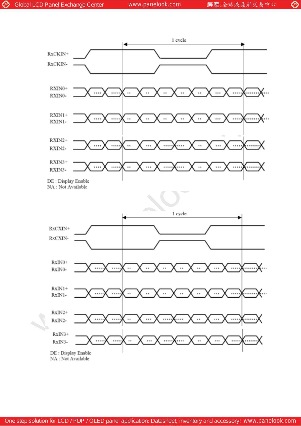
4-3 Interface block diagram
Page 9

Global LCD Panel Exchange Center
www.panelook.com
One step solution for LCD / PDP / OLED panel application: Datasheet, inventory and accessory!
www.panelook.com
(Computer side) (TFT-LCD side)
(1) 8bit Mode LVDS_SET=H (20 pin=3.3[v])
(2) 8bit Mode LVDS_SET=L (20 pin=GND or OPEN)
(3) 6bit Mode LVDS_SET=L (20 pin=GND or OPEN )
4-4 Backlight
Page 10

Global LCD Panel Exchange Center
www.panelook.com
One step solution for LCD / PDP / OLED panel application: Datasheet, inventory and accessory!
www.panelook.com
CN 2, 3 , 4,5
The module-side connector : BHSR-02VS-1 (JST)
The user-side connector : SM02B-BHSS-1-TB (JST)
Pin no. symbol I/O Function
V
1
2
HIGH
V
LOW
CN2
CN3
CN4
CN5
I Power supply for lamp (High voltage side)
I Power supply for lamp (Low voltage side)
Red cable is V
HIGH
White cable is V
Blue cable is V
Gray cable is V
Red cable is V
White cable is V
Blue cable is V
Gray cable is V
HIGH
LOW
HIGH
LOW
LOW
HIGH
LOW
TFT LCD back view
5. Absolute Maximum Ratings
Parameter Symbol Condition Ratings Unit Remark
Supply voltage Vcc Ta=25
Lamp Input voltage VHIGH
Storage temperature T
Operating temperature T
STG
OPA
-
-
-
0 ~+ 4.0
0 ~ + 2700
25 ~ + 60
0 ~ + 50
V
Vrms
℃
℃
【Note 1】 Humidity :95%RH Max. ( Ta=40 )
Maximum wet-bulb temperature at 39 or less. ( Ta>40 )
No condensation.
Note1
Note1
6. Electrical Characteristics
Page 11

Global LCD Panel Exchange Center
www.panelook.com
One step solution for LCD / PDP / OLED panel application: Datasheet, inventory and accessory!
www.panelook.com
6-1. TFT-LCD panel driving Ta=25℃
Parameter Symbol Min. Typ. Max. Unit Remark
Vcc
Permissive input ripple voltage VRF 100 mVp-p Vcc=+3.3V
Differential input Hight VTH +100 mV
hreshold voltage Low VTL –100 mV
Input current (High) IOH 10 A VI=2.4V, Vcc=3.6V
Input current (Low) IOL 10 A VI=0V, Vcc=3.6V
Terminal resistor RT 100 Differential input
Note1 VCM : Common mode voltage of LVDS driver.
Note2
1) On-off sequences of Vcc
and data
0<t1<=10ms
0<t2<=10ms
0<t3<=1s
1s<=t4
Supply voltage Vcc +3.0 +3.3 +3.6 V Note2
Current dissipation Icc 425 700 mA Note3
VCM=+1.2V
Note1
200ms<=t5
Power sequence for Backlight is not especially specified, however it is recommended to consider some
timing difference between LVDS input and Backlight input as shown above.
If the Backlight lights on before LCD starting, or if the Backlight is kept on after LCD stopping, the screen
may look white for a moment or abnormal image may be displayed.
This is caused by variation in output signal from timing generator at LVDS input on or off. It does not
cause the damage to the LCD module.
2)Dip conditions for supply voltage
1) V2 ≤Vcc<V1
td ≤ 10ms
2) Vcc<V2
Vcc-dip conditions should also
follow the on-off conditions.
【Note3】Typical current situation : 16-gray-bar pattern
Vcc=+3.3V, CK=65MHz
Horizontal period =20.7 us
Gray scale : GS(4n)
n=0~15
The explanation of each gray scale, GS(4n), is described below section 8-2.
6-2. Backlight
Page 12

Global LCD Panel Exchange Center
www.panelook.com
One step solution for LCD / PDP / OLED panel application: Datasheet, inventory and accessory!
www.panelook.com
The back light system is an edge-lighting type with 4 CCFTs (Cold Cathode Fluorescent Tube).
The characteristics of the lamp are shown in the following table.
The value mentioned below is at the case of one CCFT.
Parameter Symbol Min. Typ. Max. Unit Remark
Lamp current range IL 5.0 6.0 - mArms Note1
Lamp voltage VL 558 572 - Vrms IL=4.5 mArms Ta=25 60kHz
Lamp power consumption
Lamp frequency FL
P
L
- 3.4 4.0 W
49 50 -
Note2
IL=4.5 mArms Ta=25 60kHz
kHz Note3
Kick-off voltage Vs
Lamp life time TL
562 601 -
- 40,000 -
Vrms
hour Note5
Ta=0℃ 60kHz [Note4]
【Note1】 A lamp can be light in the range of lamp current shown above.
Maximum rating for current is measured by high frequency current measurement equipment
connected to V
LOW at circuit showed below.
(Note : To keep enough kick-off voltage and necessary steady voltage for CCFT.)
Lamp frequency : 40~70kHz
Ambient temperature : 0~50℃
CN 2,3,4,5
Inverter
Module
【Note2】
【Note3】Lamp frequency of inverter may produce interference with horizontal synchronous frequency, and
【Note4】This is transformer output voltage at 33pF for the ballast capacitor of a DC-AC inverter.
Referential data per one CCFT by calculation ( IL×VL ) .
The data don’t include loss at inverter.
this may cause horizontal beat on the display. Therefore, adjust lamp frequency, and keep inverter
as far as from module or use electronic shielding between inverter and module to avoid interference.
The kick-off voltage may rise up in the user set, please decide the open output voltage by
checking not to occur lighting failure under operating state.
The open output voltage should be applied to the lamp for more than 1 second to startup.
Otherwise the lamp may not be turned on.
CN 2,3,4,5
【Note5】
Lamp life time is defined as the time when either (1) or (2) occurs in the continuous operation under
the condition of Ta=25℃ and IL=6.0 mA rms.
(1)Brightness becomes 50% of the original value under standard condition.
(2) Kick-off voltage at Ta=0℃ exceeds 2200 V
rms
value.
Page 13

Global LCD Panel Exchange Center
www.panelook.com
One step solution for LCD / PDP / OLED panel application: Datasheet, inventory and accessory!
www.panelook.com
<<Note>>
The performance of the backlight, for example lifetime or brightness, is much influenced by the
characteristics of the DC-AC inverter for the lamp. When you design or order the inverter, please make
sure that a poor lighting caused by the mismatch of the backlight and the inverter (miss-lighting, flicker,
etc.) never occurs. When you confirm it, the module should be operated in the same condition as it is
installed in your instrument.
Use the lamp inverter power source incorporating such safeguard as overvoltage / overcurrent protective
circuit or lamp voltage waveform detection circuit, which should have individual control of each lamp.
In case one circuit without such individual control is connected to more than two lamps, excessive current
may flow into one lamp when the other one is not in operation.
7. Timing characteristics of input signals
7-1. Timing characteristics
Parameter Symbol Min. Typ. Max. Unit
Clock signal Frequency 1/Tc 50.0 65.0 80.0 MHz
ENAB signal
Horizontal period TH
Horizontal period(High) THd 1024 1024 1024 clock
Vertical period TV 773 806 990 line
Vertical period (High) TVd 768 768 768 line
【Note】 In case of using the long vertical period, the deterioration of display quality, flicker etc. may occur.
1056 1344 1720 clock
16.0 20.7 23.4 µs
7-2 Input Data Signals and Display Position on the screen
Page 14

Global LCD Panel Exchange Center
www.panelook.com
One step solution for LCD / PDP / OLED panel application: Datasheet, inventory and accessory!
www.panelook.com
8. Input Signals, Basic Display Colors and Gray Scale of Each Color
Page 15

Global LCD Panel Exchange Center
www.panelook.com
One step solution for LCD / PDP / OLED panel application: Datasheet, inventory and accessory!
www.panelook.com
8-1 8bit input
Date signal
Basic
Color
Gray
Scale
of
Red
Gray
Scale
of
Green
Gray
Scale
of
Blue
Colors&
Gray
Black
Blue
Green
Cyan
Red
Magenta
Yellow
White
Black GS0 0 0 0 0 0 0 0 0 0 0 0 0 0 0 0 0 0 0 0 0 0 0 0 0
↑
Darker GS2 0 1 0 0 0 0 0 0 0 0 0 0 0 0 0 0 0 0 0 0 0 0 0 0
↑ ↓ ↓ ↓ ↓
↓ ↓ ↓ ↓ ↓
Brighter GS250 0 1 0 1 1 1 1 1 0 0 0 0 0 0 0 0 0 0 0 0 0 0 0 0
↓
Red GS252 X X 1 1 1 1 1 1 0 0 0 0 0 0 0 0 0 0 0 0 0 0 0 0
Black GS0 0 0 0 0 0 0 0 0 0 0 0 0 0 0 0 0 0 0 0 0 0 0 0 0
↑
Darker GS2 0 0 0 0 0 0 0 0 0 1 0 0 0 0 0 0 0 0 0 0 0 0 0 0
↑ ↓ ↓ ↓ ↓
↓ ↓ ↓ ↓ ↓
Brighter GS250 0 0 0 0 0 0 0 0 0 1 0 1 1 1 1 1 0 0 0 0 0 0 0 0
↓
Green GS252 0 0 0 0 0 0 0 0 X X 1 1 1 1 1 1 0 0 0 0 0 0 0 0
Black GS0 0 0 0 0 0 0 0 0 0 0 0 0 0 0 0 0 0 0 0 0 0 0 0 0
↑
Darker GS2 0 0 0 0 0 0 0 0 0 0 0 0 0 0 0 0 0 1 0 0 0 0 0 0
↑ ↓ ↓ ↓ ↓
↓ ↓ ↓ ↓ ↓
Brighter GS250 0 0 0 0 0 0 0 0 0 0 0 0 0 0 0 0 0 1 0 1 1 1 1 1
↓
Blue GS252 0 0 0 0 0 0 0 0 0 0 0 0 0 0 0 0 X X 1 1 1 1 1 1
Gray
scale
GS251 0 1 0 1 1 1 1 1 0 0 0 0 0 0 0 0 0 0 0 0 0 0 0 0
GS251 0 0 0 0 0 0 0 0 1 1 0 1 1 1 1 1 0 0 0 0 0 0 0 0
GS251 0 0 0 0 0 0 0 0 0 0 0 0 0 0 0 0 1 1 0 1 1 1 1 1
R0 R1 R2 R3 R4 R5 R6 R7 G0 G1 G2 G3 G4 G5 G6 G7 B0 B1 B2 B3 B4 B5 B6 B7
S
cale
─
0 0 0 0 0 0 0 0 0 0 0 0 0 0 0 0 0 0 0 0 0 0 0 0
─
0 0 0 0 0 0 0 0 0 0 0 0 0 0 0 0 X X 1 1 1 1 1 1
─
0 0 0 0 0 0 0 0 X X 1 1 1 1 1 1 0 0 0 0 0 0 0 0
─
0 0 0 0 0 0 0 0 X X 1 1 1 1 1 1 X X 1 1 1 1 1 1
─
X X 1 1 1 1 1 1 0 0 0 0 0 0 0 0 0 0 0 0 0 0 0 0
─
X X 1 1 111100000000 X X 1 1 1111
─
X X 1 1 1 1 1 1 X X 1 1 1 1 1 1 0 0 0 0 0 0 0 0
─
X X 1 1 1 1 1 1 X X 1 1 1 1 1 1 X X 1 1 1 1 1 1
GS1 1 0 0 0 0 0 0 0 0 0 0 0 0 0 0 0 0 0 0 0 0 0 0 0
GS1 0 0 0 0 0 0 0 0 1 0 0 0 0 0 0 0 0 0 0 0 0 0 0 0
GS1 0 0 0 0 0 0 0 0 0 0 0 0 0 0 0 0 1 0 0 0 0 0 0 0
0 : Low level voltage, 1 : High level voltage. X :Don’t care.
Each basic color can be displayed in 253 gray scales from 8 bit data signals. According to the combination of
total 24 bit data signals, the 16-million-color display can b e achieved on the screen.
Basic Color Gray Scale of Red Gray Scale of Green Gray Scale of Blue
8-2 6bit input
Page 16

Global LCD Panel Exchange Center
www.panelook.com
One step solution for LCD / PDP / OLED panel application: Datasheet, inventory and accessory!
www.panelook.com
Date signal
Basic
Color
Gray
Scale
Red
Colors&
ray scale
G
Black ─ 0 0 0000000000 0 0 0 000
Blue ─ 0 0 0000000000 1 1 1 111
Green ─ 0 0 0000111111 0 0 0 000
Cyan ─ 0 0 0000111111 1 1 1 111
Red ─ 1 1 1111000000 0 0 0 000
Magenta ─ 1 1 1111000000 1 1 1 111
Yellow ─ 1 1 1111111111 0 0 0 000
White ─ 1 1 1111111111 1 1 1 111
Black GS0 0 0 0000000000 0 0 0 000
↑ GS1 1 0 0000000000 0 0 0 000
Darker GS2 0 1 0000000000 0 0 0 000
of
↑ ↓ ↓ ↓ ↓
↓ ↓ ↓ ↓ ↓
Brighter GS61 1 0 1111000000 0 0 0 000
↓ GS62 0 1 1111000000 0 0 0 000
Red GS63 1 1 1111000000 0 0 0 000
Gray
Scale
R0 R1 R2 R3 R4 R5 G0 G1 G2 G3 G4 G5 B0 B1 B2 B3 B4 B5
Black GS0 0 0 0000000000 0 0 0 000
↑ GS1 0 0 0000100000 0 0 0 000
Darker GS2 0 0 0000010000 0 0 0 000
Gray
Scale
of
Green
Gray
Scale
of
Blue
↑ ↓ ↓ ↓ ↓
↓ ↓ ↓ ↓ ↓
Brighter GS61 0 0 0000101111 0 0 0 000
↓ GS62 0 0 0000011111 0 0 0 000
Green GS63 0 0 0 0 0 0 111111 0 0 0 000
Black GS0 0 0 0000000000 0 0 0 000
↑ GS1 0 0 0000000000 1 0 0 000
Darker GS2 0 0 0000000000 0 1 0 000
↑ ↓ ↓ ↓ ↓
↓ ↓ ↓ ↓ ↓
Brighter GS61 0 0 0000000000 1 0 0 111
↓ GS62 0 0 0000000000 0 1 1 111
Blue GS63 0 0 0000000000 1 1 1 111
0 : Low level voltage, 1 : High level voltage.
Each basic color can be displayed in 64 gray scales from 6 bit data signals. According to the combination
of total 18 bit data signals, the 262,144-color display
can be achieved on the screen.
9. Optical Characteristics
Page 17

Global LCD Panel Exchange Center
www.panelook.com
One step solution for LCD / PDP / OLED panel application: Datasheet, inventory and accessory!
www.panelook.com
Parameter Symbol Condition Min. Typ. Max. Unit Remark
Viewing
Vertical
angle
range
Horizontal
Vertical
Horizontal
Contrast ration CR
Response
Time
Rise
Fall
Luminance of white
White Uniformity
※The measurement shall be executed 30 minutes after
The optical characteristics shall be measured in a dark room or equivalent state with the method shown
in Fig.2 below.
Ta=25℃, Vcc =+3.3V
θ 11
θ 12
θ21, θ 22
θ11
θ12
θ21, θ 22
r
d
CR>=5
CR>=10
0
θ=0
40 55 - Deg.
70 80 - Deg.
70 80 - Deg.
30 45 - Deg.
45 55 - Deg.
50 60 - Deg.
300 350 -
- 5 20 ms
- 20 40 ms
x 0.283 0.313 0.343 Chromaticity of White
y 0.299 0.329 0.359
x 0.551 0.581 0.611 Chromaticity of Red
y 0.292 0.322 0.352
x 0.277 0.307 0.337 Chromaticity of Green
θ=0
0
y 0.516 0.546 0.576
x 0.121 0.151 0.181 Chromaticity of Blue
y 0.097 0.127 0.157
Y
200 260 - cd/m2
L
W
- - 1.25 -
lighting at rating.
【Note1,4】
【Note2,4】
【Note3,4】
【Note 4】
IL=4.5mArms
Fl=60kHz
【Note 4】
【Note 5】
【Note1】Definitions of viewing angle range:
Page 18

Global LCD Panel Exchange Center
www.panelook.com
One step solution for LCD / PDP / OLED panel application: Datasheet, inventory and accessory!
www.panelook.com
【Note2】Definition of contrast ratio:
The contrast ratio is defined as the following.
Contrast Ratio (CR) =
【Note3】Definition of response time:
The response time is defined as the following figure and shall be measured by switching the input
signal for "black" and "white".
【Note4】This shall be measured at center of the screen.
Luminance (brightness) with all pixels white
Luminance (brightness) with all pixels black
【Note5】Definition of white uniformity:
White uniformity is defined as the following with five measurements (A~E).
10. Handling Precautions
Page 19

Global LCD Panel Exchange Center
www.panelook.com
One step solution for LCD / PDP / OLED panel application: Datasheet, inventory and accessory!
www.panelook.com
a) Be sure to turn off the power supply when inserting or disconnecting the cable.
b) Be sure to design the cabinet so that the module can be installed without any extra stress such as
warp or twist.
c) Since the front polarize is easily damaged, pay attention not to scratch it.
d) Since long contact with water may cause discoloration or spots, wipe off water drop immediately.
e) When the panel surface is soiled, wipe it with absorbent cotton or other soft cloth.
f) Since the panel is made of glass, it may break or crack if dropped or bum
Handle with care.
g) Since CMOS LSI is used in this module, take care of static electricity
consideration when handling.
h) Make sure the four mounting holes of the module are grounded sufficiently. Take electro-magnetic
interference (EMI) into consideration.
i) The module has some printed circuit boards (PCBs) on the back side. Take care to keep them
stress or pressure when handling or installing the module; otherwise some of electronic parts on the
PCBs m
j) Observe all other precautionary requirements in handling components.
k) When some pressure is added onto the module from rear side constantly, it causes display
l) When handling LCD modules and assembling them into cabinets, please be noted that long-term
storage in the environment of oxidization or deoxidization gas and the use of such m
solvent, adhesive, resin, etc. which generate these gasses, may cause corrosion and discoloration of the
LCD modules.
11. Packing form
ay be damaged.
non-uniform
ity issue, functional defect, etc. So, please avoid such design.
ped on hard surface.
and take the human earth into
form any
aterials as reagent,
a) Production country : JAPAN , TAIWAN, CHINA
b) Piling number of cartons : m
c) Packing quantity in one carton : 10 modules
d) Carton size : 408mm(W)×340m
e) total mass of one carton filled with full m
12 Reliability
test items
aximum 6 cartons
m(H)×398mm(D)
odules : 12.0kg(typ.)
Page 20

Global LCD Panel Exchange Center
www.panelook.com
One step solution for LCD / PDP / OLED panel application: Datasheet, inventory and accessory!
www.panelook.com
No. Test item Conditions
1 High temperature storage test
2 Low temperature storage test
3 High temperature
& high humidity operation test
4 High temperature operation test
5 Low temperature operation test
6 Vibration test(non- operating)
Ta = 60℃ 240h
Ta = -25℃ 240h
Ta = 40℃ ; 95%RH 240h
(No condensation)
Ta = 60℃ 240h
(The temperature of panel surface)
Ta = 0℃ 240H
Waveform : Sine wave
Frequency : 10 57Hz/Vibration width (one side) : 0.075mm
: 58~500Hz/Gravity
Sweep time : 11minutes
Test period : 3 hours
(1 hour for each direction of X,Y,Z)
7 Shock test(non- operating) Max. gravity : 490m/s2
Pulse width : 11ms, sine wave
Direction : ±
X, ±Y, ±Z,
once for each direction.
8 Thermal shock test(Storage)
Ta=-25℃~60℃
; 5 cycles
Test period : 10 hours (1 hour for each temperature)
: 9.8m/s2
9 Altitude
Ta=50℃
Ta=70℃
,70kPa,3,048m(10,000ft), t=24h (Operating)
,12kPa,15,240m(50,000ft), t=24h (Storage)
[Result Evaluation Criteria]
Under the display quality test conditions with normal operation state, these shall be no change
which may affect practical display function.
Fig.1. Outline dimensions
Page 21

Global LCD Panel Exchange Center
www.panelook.com
One step solution for LCD / PDP / OLED panel application: Datasheet, inventory and accessory!
www.panelook.com
 Loading...