

Page 1
XL-G5000V/XL-G5000V(S)
SERVICE MANUAL
No. XXXXXXXXXXXXX
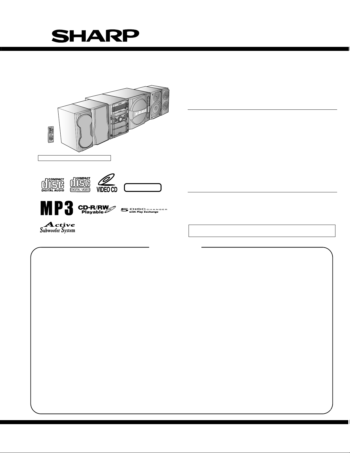
VIDEO CD MICRO SYSTEM
XL-G5000V
XL-G5000V(S)
XL-G5000V(S) is silver color of XL-G5000V
*
NTSC/PAL
MODEL
XL-G5000V Video CD Micro System consisting of XL-G5000V
(main unit) and CP-G5000V (front speaker).
XL-G5000V(S) Video CD Micro System consisting of XL-G5000V(S)
(main unit) and CP-G5000V (front speaker).
MODEL
• In the interests of user-safety the set should be restored to its original
CONTENTS
XL-G5000V
XL-G5000V(S)
SPEAKER SYSTEM
CP-G5000
CP-G5000(S)
CP-G5000 Speaker System consisting of CP-SW5000
(Active unit) and GBOXSA052AWM1 (surround speaker).
CP-G5000(S) Speaker System consisting of CP-SW5000(S)
(Active unit) and GBOXSA066AWM1 (surround speaker).
condition and only parts identical to those specified be used.
PRECAUTIONS FOR USING LEAD-FREE SOLDER
CHAPTER 1. GENERAL DESCRIPTION
[1] SPECIFICATIONS......................................... 1-1
[2] NAMES OF PARTS........................................1-1
CHAPTER 2. ADJUSTMENTS
[1] ADJUSTMENT............................................... 2-1
[2] TEST MODE..................................................2-3
[3] Standard Specification of Stereo System
Error Message Display Contents ................... 2-5
CHAPTER 3. MECHANICAL DESCRIPTION
[1] REMOVING AND REINSTALLING THE
MAIN PARTS ................................................. 4-1
[2] DISASSEMBLY.............................................. 3-3
CHAPTER 4. DIAGRAMS
[1] BLOCK DIAGRAM.........................................5-1
CHAPTER 5. CIRCUIT DESCRIPTION
[1] WAVEFORMS OF CD CIRCUIT....................6-1
[2] VOLTAGE......................................................5-2
CHAPTER 6. CIRCUIT SCHEMATICS AND PARTS
LAYOUT
[1] NOTES ON SCHEMATIC DIAGRAM............7-1
[2] TYPES OF TRANSISTOR AND LED............6-1
[3] WIRING SIDE OF PWB/SCHEMATIC DIA-
GRAM............................................................6-2
CHAPTER 7. FLOWCHART
[1] TROUBLESHOOTING ..................................8-1
CHAPTER 8. OTHERS
[1] FUNCTION TABLE OF IC.............................8-1
[2] FL DISPLAY ................................................8-11
CHAPTER 9. ACTIVE SUBWOOFER DIAGRAM
[1] WIRING SIDE OF PWB/SCHEMATIC DIA-
GRAM........................................................... 9-1
Parts Guide
SHARP CORPORATION
This document has been published to be used
for after sales service only.
The contents are subject to change without notice.
Page 2
XL-G5000V/XL-G5000V(S)
SAFETY PRECAUTION FOR SERVICE MANUAL
Precaution to be taken when replacing and servicing the Laser Pickup.
The AEL (Accessible Emission Level) of Laser Power Output for this model is specified to be lower than Class 1 Requirements.
However, the following precautions must be observed during servicing to protect your eyes against exposure to the Laser beam.
1. When the cabinet has been removed, the power is turned on without a compact disc, and the Pickup is on a position outer than the
lead-in position, the Laser will light for several seconds to detect a disc. Do not look into the Pickup Lens.
2. The Laser Power Output of the Pickup inside the unit and replacement service parts have already been adjusted prior to shipping.
3. No adjustment to the Laser Power should be attempted when replacing or servicing the Pickup.
4. Under no circumstances look directly into the Pickup Lens at any time.
5. CAUTION - Use of controls or adjustments, or performance of procedures other than those specified herein may result in
hazardous radiation exposure.
VOLTAGE SELECTION
Before operating the unit on mains, check the preset voltage. If the voltage is different from your local voltage, adjust the voltage
as follows.
Turn the selector with a screwdriver until the appropriate voltage number appears in the window (110V,127V,220V or 230V 240V AC).
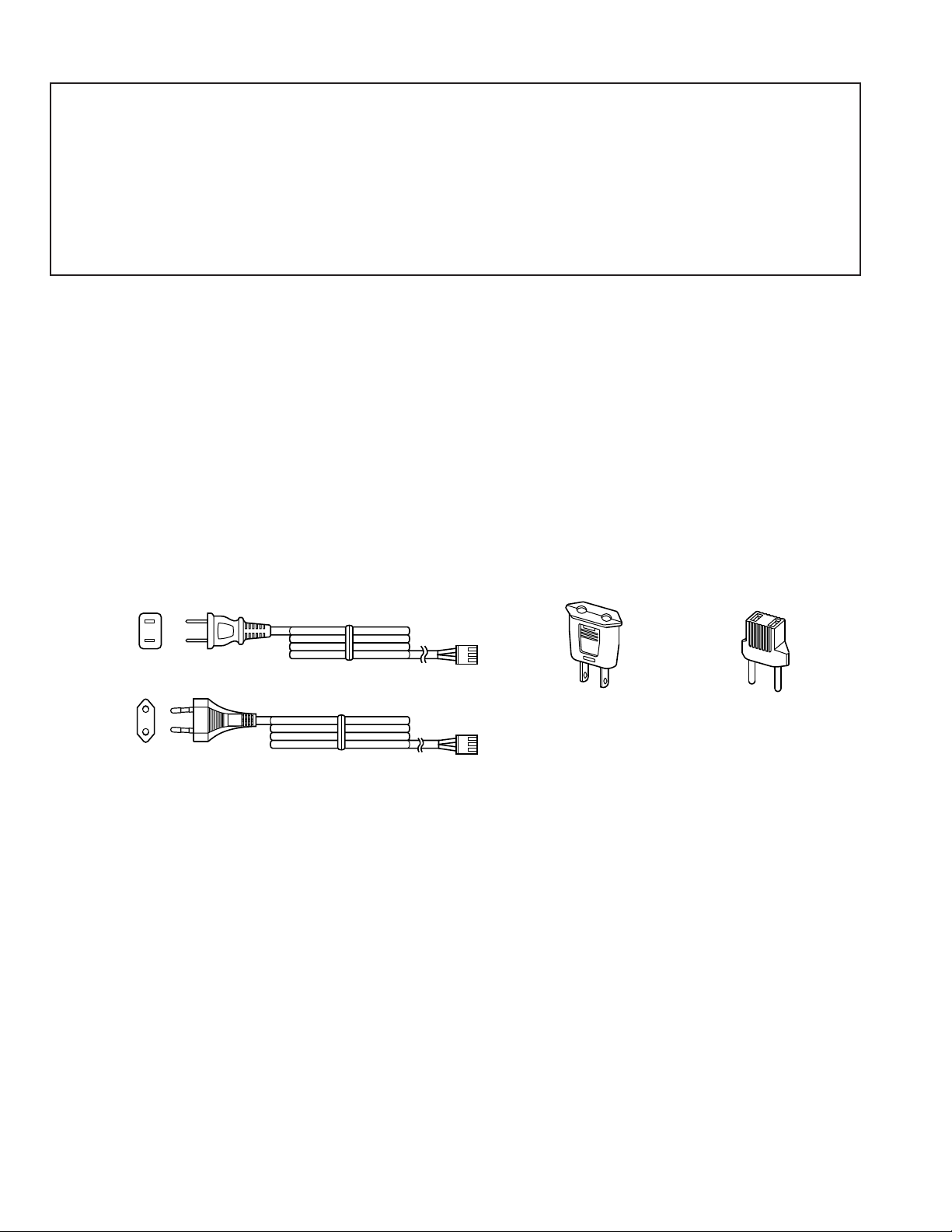
AC POWER SUPPLY CORD AND AC PLUG ADAPTOR
QACCA0008AW00
QACCE0015AW00
QPLGA0003AWZZ
QPLGA0004AWZZ
– i –
Page 3
XL-G5000V/XL-G5000V(S)
AudioXL-HP404VService ManualXLHP404VMarketE
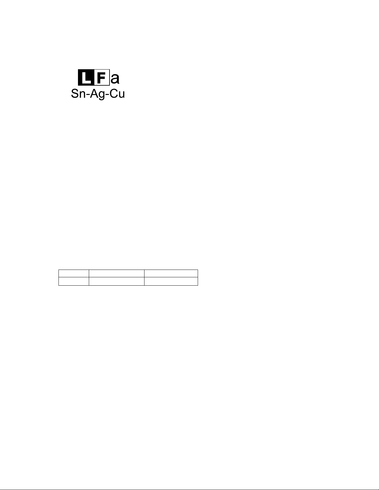
PRECAUTIONS FOR USING LEAD-FREE SOLDER
1. Employing lead-free solder
"VCD PWB" of this model employs lead-free solder. The LF symbol indicates lead-free solder, and is attached on the PWB and
service manuals. The alphabetical character following LF shows the type of lead-free solder.
Example:
Indicates lead-free solder of tin, silver and copper.
2. Using lead-free wire solder
When fixingthe PWBsoldered with the lead-free solder,apply lead-freewire solder. Repairing with conventionallead wiresolder
may cause damage or accident due to cracks.
As the melting point of lead-free solder (Sn-Ag-Cu) is higher than the lead wire solder by 40 C, we recommend you to use a
dedicated soldering bit, if you are not familiar with how to obtain lead-free wire solder or soldering bit, contact our service station
or service branch in your area.
3. Soldering
As the melting point of lead-free solder (Sn-Ag-Cu) is about 220 C which is higher than the conventional lead solder by 40 C,
and as it has poor solder wettability, you may be apt to keep the soldering bit in contact with the PWB for extended period of
time. However, Since the land may be peeled off or the maximum heat-resistance temperature of parts may be exceeded,
remove the bit from the PWB as soon as you confirm the steady soldering condition.
Lead-free solder contains more tin, and the end of the soldering bit may be easily corrected. Make sure to turn on and off the
power of the bit as required.
If a different type of solder stays on the tip of the soldering bit, it is alloyed with lead-free solder. Clean the bit after every use
of it.
When the tip of the soldering bit is blackened during use, file it with steel wool or fine sandpaper.
Be careful when replacing parts with polarity indication on the PWB silk.
Lead-free wire solder for servicing
Ref No. DescriptionParts No.
PWB-D 92LPWB5619VCDS VCD
Page 4
AudioXL-G5000VService ManualXL-G5000VMarketE
CHAPTER 1. GENERAL DESCRIPTION
FOR A COMPLETE DESCRIPTION OF THE OPERATION OF THIS UNIT, PLEASE REFER
TO THE OPERATION MANUAL.
[1] SPECIFICATIONS
XL-G5000V
■
General
Power source AC 110/127/220/230 - 240 V, 50/60Hz
Power consumption
Dimensions Width : 185 mm (7-1/4")
Weight
■
Amplifier
Output power Front speakers:
Output terminals
Input terminals
■
Video CD
Video output format PAL/NTSC
90 W
Height : 260 mm (10-1/4")
Depth : 307 mm (12")
6.4 kg (14.1 lbs.)
MPO: 256 W (128 W + 128 W) (10% T.H.D.)
RMS: 130 W (65 W + 65 W) (10% T.H.D.)
RMS: 122 W (81 W +81 W) (1% T.H.D.)
Surround speakers:
MPO:128 W (64 W + 64 W) (10% T.H.D.)
RMS: 70 W (35 W + 35 W) (10% T.H.D.)
RMS: 60 W (30 W +30 W) (1% T.H.D.)
Speakers: 6 ohms
Headphones: 16 - 50 ohms (recommended:
32 ohms)
Subwoofer pre-output (audio signal):
200 mV/10 k ohms at 70 Hz
Video out: 1Vp-p (75ohms)
Video/auxiliary (audio signal):
500 mV/47 k ohms
Microphone 1/2: 1 mV/600 ohms
CP-G5000 (Front Speaker)
Type 2-way type speaker system
Maximum input power
Rated input power 65 W
Impedance 8 ohms
Dimensions
Weight 3.0 kg (6.6 lbs.)/each
GBOXSA052AWM1 (Surround Speaker)
Type
Maximum input power
Rated input power 35 W
Impedance 16 ohms
Dimensions
Weight 2.5 kg (5.5 lbs.)/each
CP-SW5000 (Subwoofer)
XL-G5000V/XL-G5000V(S)
5 cm (2") tweeter
13 cm (5-1/8") woofer
130 W
Width : 165 mm (6-1/2")
Height : 260 mm (10-1/4")
Depth : 231mm (9-15/16")
Full-range speaker system
8 cm (3 1/8") woofer (x2)
70 W
Width : 120 mm (4-3/4")
Height : 260 mm (10-1/4")
Depth : 227mm (8-15/16")
■
CD player
Type 5-disc multi-play compact disc player
Signal readout Non-contact, 3-beam semiconductor laser
D/A converter 1-bit D/A converter
Frequency response 20 - 20,000 Hz
Dynamic range 90 dB (1 kHz)
■
Tuner
Frequency range FM: 88.0 - 108.0 MHz
■
Cassette deck
Frequency response 50 - 14,000 Hz (normal tape)
Signal/noise ratio 50 dB (recording/playback)
Wow and flutter 0.3 % (WRMS)
pickup
AM: 531 - 1,602 kHz
Power source AC 110/127/220/230 - 240 V, 50/60 Hz
Power consumption 90 W
Output power
Input terminals Subwoofer input (audio signal):
Speaker type 20 cm (7-7/8") woofer
Impedance 6 ohms
Dimensions
Weight 11.8 kg (26.0 lbs.)
Specifications for this model are subject to change without prior notice.
MPO: 340 W (170W+170W)(10%T.H.D.)
RMS: 200 W (100 W + 100 W) (10% T.H.D.)
RMS: 140 W (70 W +70 W) (0.9% T.H.D.)
200 mV / 10 k ohms at 70 Hz
Width : 320 mm (12-5/8")
Height : 260 mm (10-1/4")
Depth : 394mm (15-1/2")
1 – 1
Page 5
XL-G5000V/XL-G5000V(S)
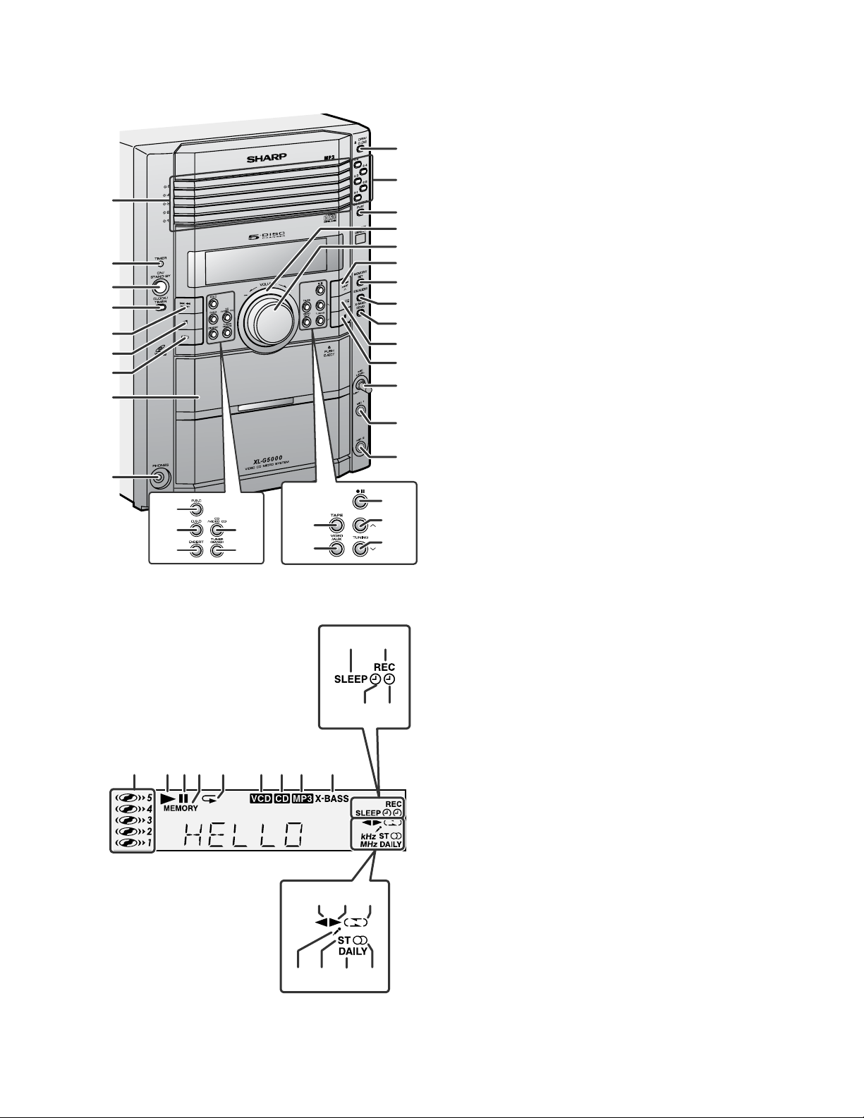
[2] NAMES OF PARTS
1
2
3
4
5
6
7
8
9
24
25 27
■ Front panel
1. Disc Trays
2. Timer Indicator
3. On/Stand-by Button
10
11
12
13
14
15
16
17
18
19
20
21
22
23
31
29
2826
30
32
33
4. Clock/Ti mer Button
5. Video CD Skip or Previous, CD/MP3 Disc Track Down or
Fast Reverse, Tape Fast Wind, Tuner Preset Down,
Time Down Button
6. Tape Reverse Play Button
7. Tape Reverse Mode Select Button
8. Cassette Compartment
9. Headphone Socket
10. Disc Tray Open/Close Button
11. Disc Number Select Buttons
12. Disc Direct Play Button
13. Illumination Light
14. Volume Control
15. Video CD Skip or Next, CD/MP3 Disc Track Up or
Fast Forward, Tape Fast Wind, Tuner Preset Up,
Time Up Button
16. Memory/Set Button
17. Equaliser Mode Select Button
18. Extra Bass/Demo Mode Button
19. Video CD Play or Repeat or Select or Resume,
CD/MP3 Disc Play or Repeat,
Tape Forward Play Button
20. Video CD Stop or Return,
CD/MP3 Disc/Tape Stop Button
21. Microphone Level Control
22. Microphone Socket 1
23. Microphone Socket 2
24. Video CD Playback Control Button
25. Video CD On Screen Display On/Off Button
26. Video CD Digest/Time Search Button
27. Video CD/CD/MP3 Disc Button
28. Tuner (Band) Button
29. Tape Button
30. Video/Auxiliary Button
31. Tape Record Pause Button
32. Tuning Up Button
33. Tuning Down Button
976 8321 4 5
1918 2017
1110
12 13
1614 15
■ Display
1. Disc Number Indicators
2. Disc Play Indicator
3. Disc Pause Indicator
4. Memory Indicator
5. Disc Repeat Play Indicator
6. Video CD Indicator
7. CD Indicator
8. MP3 Disc Indicator
9. E xtra Bass Indicator
10. Sleep Indicator
11. Tape Record Indicator
12. Timer Play Indicator
13. Timer Recording Indicator
14. Tape Reverse Play Indicator
15. Tape Forward Play Indicator
16. Tape Reverse Mode Indicator
17. Karaoke Mode Indicator
18. FM Stereo Mode Indicator
19. Daily Timer Indicator
20. FM Stereo Receiving Indicator
1 – 2
Page 6
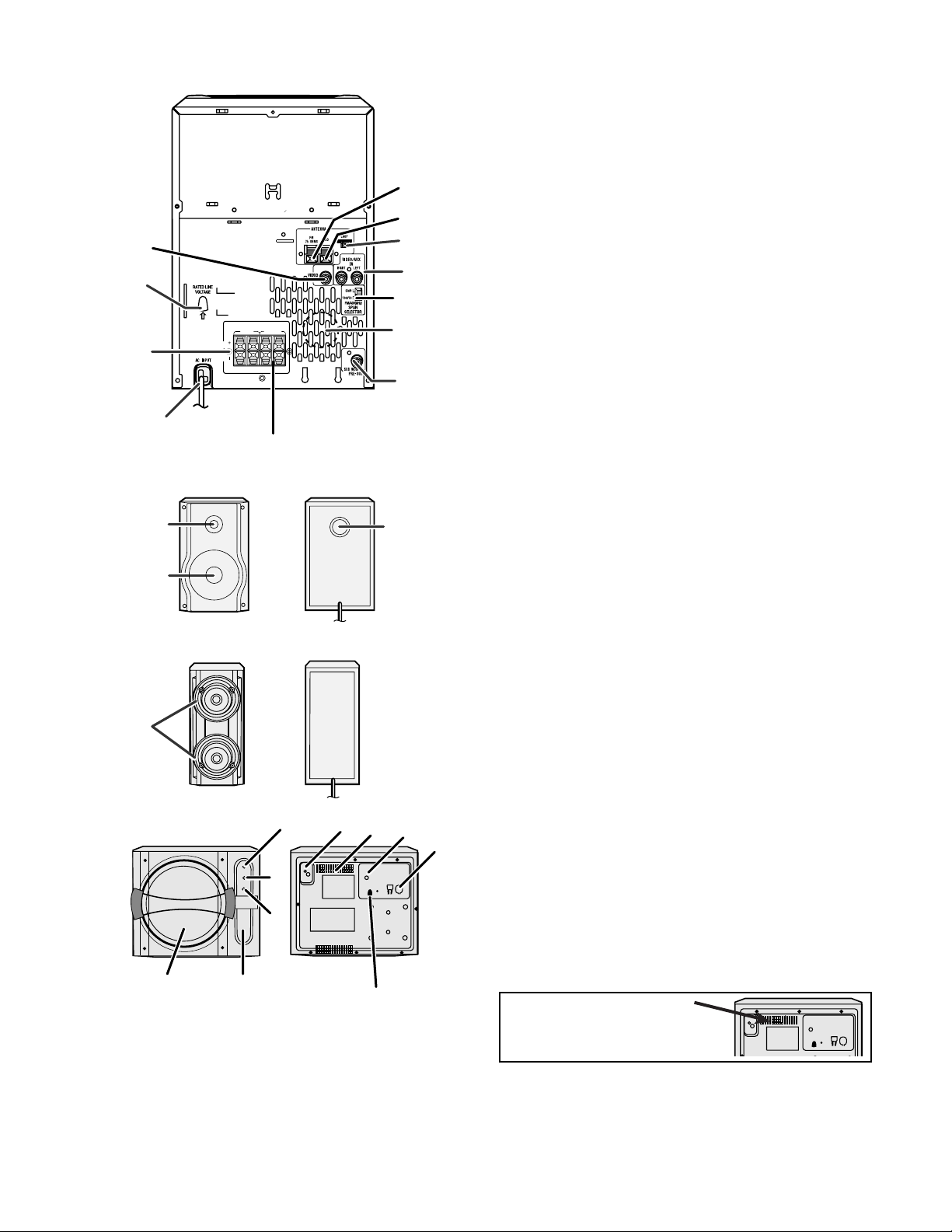
■ Rear panel
XL-G5000V/XL-G5000V(S)
6
7
1
3
8
9
10
RATEDSPEAKER IMPEDANCE:
8OHMS MIN. 16 OHMS MIN.
FRONT
SURROUND
4
SPEAKERS
LEFT
RIGHT LEFT
RIGHT
2
1. Video Output Socket
2. Cooling Fan
3. AC Voltage Selector
4. Front Speaker Terminals
5. AC Power Lead
6. FM 75 Ohms Aerial Terminal
7. FM Aerial Earth Terminal
8. AM Loop Aerial Socket
9. Video/Auxiliary (Audio Signal) Input Sockets
10. Span Selector Switch
11. Subwoofer Pre-output Socket
12. Surround Speaker Terminal
11
5
12
■
Front Speaker
2
3
1
1. Woofer
2. Tweeter
3. Bass Reflex Duct
■
Surround Speaker
1. Full-range Speaker
1
■
10
5
7
4
8
6
3
2
1
9
Active Subwoofer
1. Bass Reflex Duct
2. Subwoofer Unit
3. Speaker light up dimmer switch
4. Power Switch
5. Volume Control
6. Crossover Frequency Control
7. Cooling Fan
8. AC Power Lead
9. AC Voltage Selector
10. Subwoofer Input Socket
Cooling fan:
This product is equipped with a cooling
fan inside, which begins to run once the
power is on for better heat radiation.
1 – 3
Page 7
XL-G5000V/XL-G5000V(S)
10
1
11
19 24
12
20
2
3
13
14
15
21
22
23
25
26
27
28
16
4
5
6
7
8
9
29
30
31
17
32
33
18
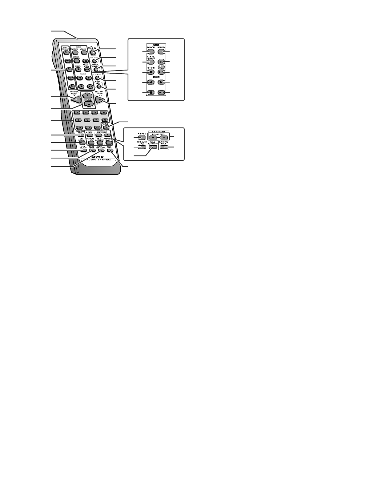
■ Remote control
1. Remote Control Transmitter
2. Disc Number Select Buttons
3. V ideo CD Skip or Previous, CD/MP3 Disc Track Down or
Fast Reverse, Tape Fast Wind, Tuner Preset Down,
Time Down Button
4. Volume Up and Down Buttons
5. Disc Direct Search Buttons
6. Equaliser Mode Select Button
7. MP3 Disc Display Button
8. Video CD On Screen Display On/Off Button
9. Video CD Bookmark Button
10. Video CD Digest/Time Search Button
11. On/Stand-by Button
12. Video CD/CD/MP3 Disc Button
13. Tuner (Band) Button
14. Tape Button
15. Video/Auxiliary Button
16. Video CD Skip or Next, CD/MP3 Disc Track Up or
Fast Forward, Tape Fast Wind, Tuner Preset Up,
Time Up Button
17. Clock/Timer Button
18. PAL/NTSC Select Button
19. Disc Random Button
20. Disc Clear/Dimmer Button
21. Video CD Stop or Return,
CD/MP3 Disc Stop Button
22. Tape Reverse Play Button
23. Tape Stop Button
24. Memory/Set Button
25. Disc Pause Button
26. Video CD Play or Repeat or Select or Resume,
CD/MP3 Disc Play or Repeat Button
27. Tape Forward Play Button
28. Tape Record Pause Button
29. Ex tra Bass Button
30. Video CD Auto/On Button
31. Video CD Playback Control Auto/Off Button
32. Echo Level Up and Down Buttons
33. Karaoke Mode Button
1 – 4
Page 8
CHAPTER 2. ADJUSTMENTS
XL-G5000V/XL-G5000V(S)
[1] ADJUSTMENT
1. MECHANISM SECTION
• Driving Force Check
Torque Meter Specified Value
Play: TW-2111 Over 80 g
• Torque Check
Torque Meter Specified Value
Play: TW-2111 30 to 80 g.cm
Fast forward: TW-2231 70 to 180 g.cm
Rewind: TW-2231 70 to 180 g.cm
2. TUNER SECTION
fL: Low-range frequency
fH: High-range frequency
• AM IF/RF
Signal generator: 400 Hz, 30%, AM modulated
Test Stage Frequency Frequency
Display
AM IF 450 kHz 1,602 kHz T351 *1
AM Band
— 531 kHz (fL): T306
Coverage
AM Tracking 990 kHz 990 kHz (fL): T303 *1
Setting/
Adjusting
Parts
1.1 ± 0.1 V
Instrument
Connection
*2
• Tape Speed
Normal
MTT-111 Variable
speed
Test Tape Adjusting
Point
Resistor in
motor.
TAPE MECHANISM
Tape
Motor
Variable Resistor in motor
Figure 1
Specified
Value
Instrument
Connection
3,000 ± 30 Hz Speaker Ter-
minal (Load
resistance: 6
ohms)
*1. Input: Antenna Output: TP302
*2. Input: Antenna Output: TP301
• FM RF
Signal generator: 1 kHz, 40 kHz dev., FM modulated
Test Stage Frequency Frequency
Display
Setting/
Adjusting
Point
FM OSC — 87.50 kHz T301 (fL):
1.3 ± 0.1 V
FM RF 98.00 MHz
98.00 MHz L312 *2
(10-30 dB)
*1. Input: Antenna Output: TP301
*2. Input: Antenna Output: Speaker terminal
• FM IF
Signal generator: 10.7MHz FM modulated
Test Stage Frequency Frequency
Display
Setting/
Adjusting
Point
IF 10.7 MHz 98 MHz T302
(Turn the
core of transformer T302
fully counterclock wise)
Instrument
Connection
*1
Instrument
Connection
*1
TUNER PWB-C
20
IC302
TP301
C393
T351
AM IF
FM ANTENNA
TERMINAL
IC301
T302
FM IF
T301
FM OSC
SO302
L312
FM RF
IC303
AM
LOOP
ANTENNA
CNP301
AM TRACKING fL
T306
AM BAND
COVERAGE fL
R356
TP302
T303
*1. Input: Antenna Output: TP301
Figure 2 ADJUSTMENT POINTS
2 – 1
Page 9
XL-G5000V/XL-G5000V(S)
3. CD SECTION
• Adjustment
Since this CD system incorporates the following automatic adjust-
ment functions, readjustment is not needed when replacing the
pickup. Therefore, different PWBs and pickups can be combined
freely.
Each time a disc is changed, these adjustments are performed
automatically. Therefore, playback of each disc can be performed
under optimum conditions.
Items adjusted automatically
1) Offset adjustment (The offset voltage between the head amplifier
output and the VREF reference voltage is compensated inside the
IC.)
* Focus offset adjustment
* Tracking offset adjustment
2) Tracking balance adjustment
3) Gain adjustment (The gain is compensated inside the IC so that the
loop gain at the gain crossover frequency will be 0 dB.)
* Focus gain adjustment
* Tracking gain adjustment
4. CD ERROR CODE DESCRIPTION
Error Explanation
01 When Pickup set inner position, inner switch cannot detect
'ON' level for 10 secs.
10* CAM error. Can't detect CAM switch when CAM is moving.
11* When it detect cam operation error during initialize process.
20* TRAY error. Can't detect TRAY switch when TRAY is mov-
ing.
21* When it detect TRAY operation error during initialize pro-
cess.
31 When it change to CD function, DSP cannot read initial data.
* 'CHECKING'
If Error is detected, 'CHECKING' will be displayed instead of 'ERCD**'. 'ER-CD**' display will only be displayed when error had been
detected for the 5th times.
2 – 2
Page 10
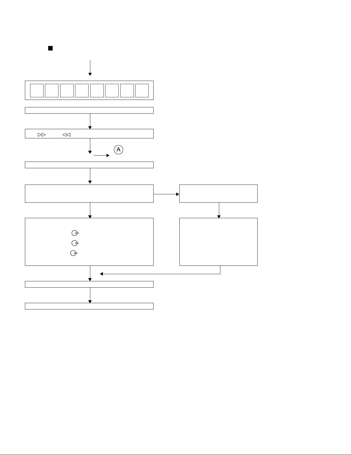
[2] TEST MODE
• Setting the test mode
During stand-by mode, press ON/STAND-BY button while pressing
down the button and X-BASS/DEMO button. then, press the CD
button to enter the test mode.
XL-G5000V/XL-G5000V(S)
CD TES T
OPEN/CLOSE operation is using manual. IL isn’t done
<< >>,<< >>buttons make pick's slide possible.
to page 2-4
<<PLAY>> key input.
Do TOC IL. Do normal play.
When these following key is input into PLAY key, track number can be appoint directly.
<< 1>> key: Track 4
<< 2>> key: Track 9
<< 3>> key: Track 15
IL isn’t done
IL isn’t done
<<MEMORY>>
key input.
Adjustment result automatically will
display as below for each 2 sec:
a) "FOF_XXXX"
b) "TOF_XXXX"
c) "TBAL_XX"
d) "TGAN_XX"
f) "FGAN_XX"
g) "RFLS_XX"
<<STOP>> key input.
STOP
explanation:
a) Focus off set = "FOF_XXXX"
b)Tracking off set = "TOF_XXXX"
c)Tracking balance = "TBAL_XX"
d)Tracking Gain = "TGAN_XX"
f) Focus Gain = "FGAN_XX"
g) RF level shift = "RFLS_XX"
VOL — Last memory
P.GEQ — FLAT
X-BASS — OFF
To cancel : Power OFF
2 – 3
Page 11
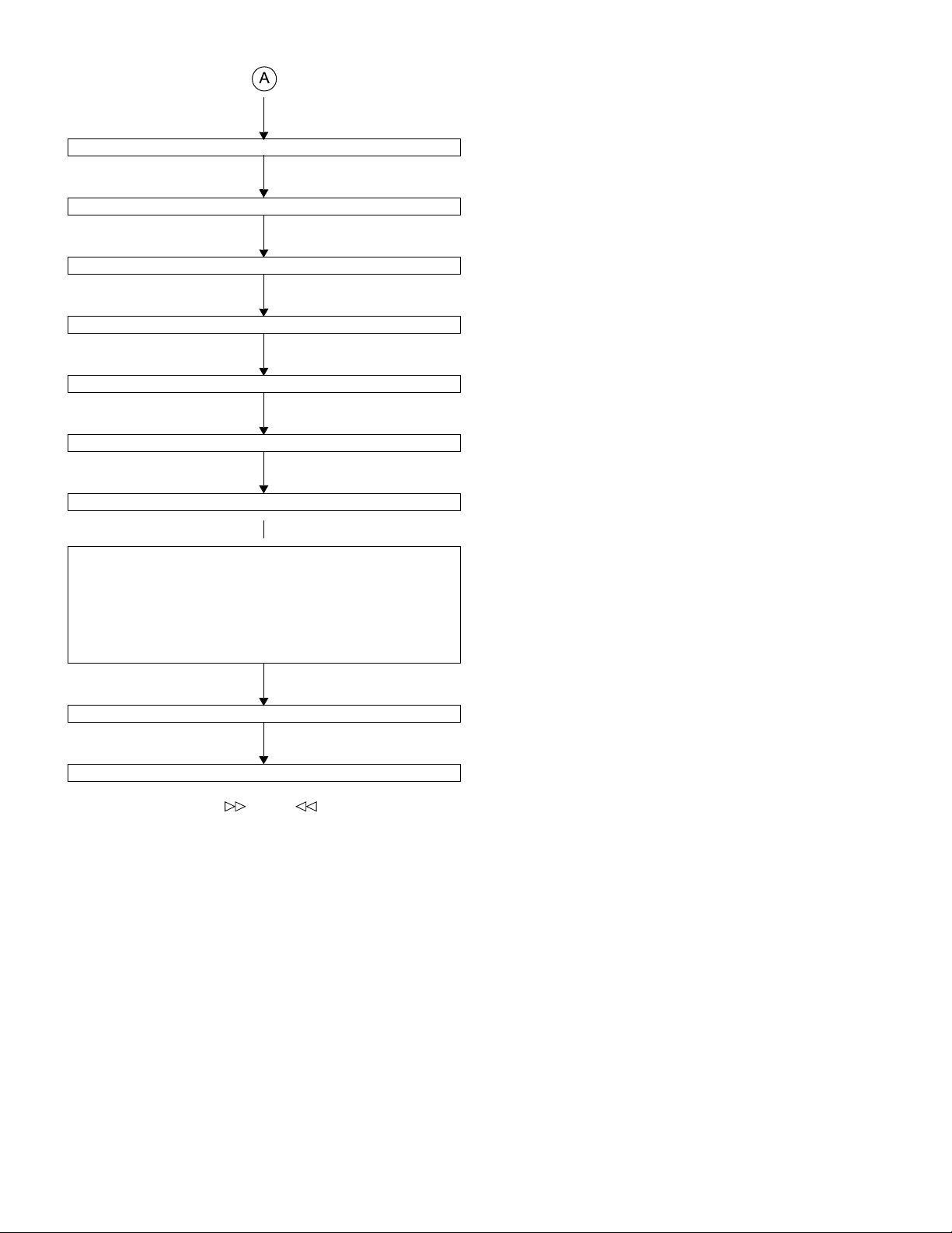
XL-G5000V/XL-G5000V(S)
<<MEMORY>> key input.
Laser ON.
<<MEMORY>> key input.
Tracking OFF play at that specific point.
<<MEMORY>> key input.
Tracking ON play from that specific point.
<<MEMORY>> key input.
Adjustment result automatically will display as below for each 2 sec :
a) "FOF_XXXX"
b) "TOF_XXXX"
c) "TBAL_XX"
d) "TGAN_XX"
f) "FGAN_XX"
g) "RFLS_XX"
<<STOP>> key input.
STOP
Sliding the PICKUP with<< >>, << >> button must only be
in STOP mode.
explanation:
a) Focus off set = "FOF_XXXX"
b)Tracking off set = "TOF_XXXX"
c)Tracking balance = "TBAL_XX"
d)Tracking Gain = "TGAN_XX"
f) Focus Gain = "FGAN_XX"
g) RF level shift = "RFLS_XX"
VOL — Last memory
BAL — CENTER
P.GEQ — FLAT
X-BASS — OFF
To cancel : Power OFF
2 – 4
Page 12

XL-G5000V/XL-G5000V(S)
[3] Standard Specification of Stereo System Error Message Display Contents
Error Contents DISPLAY Notes
CD Pickup Mechanism Error. 'ER-CD01' PU-IN SW Detection NG.
CD Changer Mechanism Error. 'ER-CD**' (*) 10: CAM SW Detection NG during normal operation
CD DSP Communication Error. 'ER-CD31' DSP COMMUNICATION ERROR.
Focus Not Match/IL Time Over. 'NO DISC'
TUNER PLL Unlock.
(*) CHECKING:
If CD changer mechanism error is detected, 'CHECKING' will be display instead of 'ER-CD**'. 'ER-CD**' display will only be display when error had
been detected for the 5 th times.
Speaker abnormal detection and +B PROTECTION display
In case speaker abnormal detection or +B PROTECTION had occurred, it can be check by pressing 'ON/STAND-BY', ' ' and 'X-BASS' button.
MicroComputer version number will displayed as "UVM****"?
Press ‘VIDEO/AUX’ button during version number display and then press ‘ON/STAND-BY’, ‘MEMORY/SET’ and ‘VIDEO/AUX’ button. Display will
show "S** B**". S is referring to speaker abnormal detection and B is referring to +B PROTECTION. ** is in hex valve.
+B PROTECTION is condition when irregular process occur on power supply line.
BEFORE TRANSPORTING THE UNIT
The following process need to be taken after set tapering/parts replacement.
1. Press the ON/STAND-BY button to enter stand-by mode.
87.50
FM MHz
11: CAM SW Detection NG during initialize process
20:TRAY SW Detection NG during normal operation
21:TRAY SW Detection NG during initialize process
PLL Unlock.
2. While pressing down the button and the X-BASS/DEMO button, press the ON/STAND-BY button. The Micro Computer version number will
be displayed as "UVM****"?
3. Press OPEN/CLOSE button until "WAIT"--> "FINISHED" appears.
4. Unplug the AC cord and the unit is ready for transporting.
2 – 5
Page 13
XL-G5000V/XL-G5000V(S)
AudioXL-G5000VService ManualXL-G5000VMarketE
CHAPTER 3. MECHANICAL DESCRIPTION
[1] REMOVING AND REINSTALLING THE
MAIN PARTS
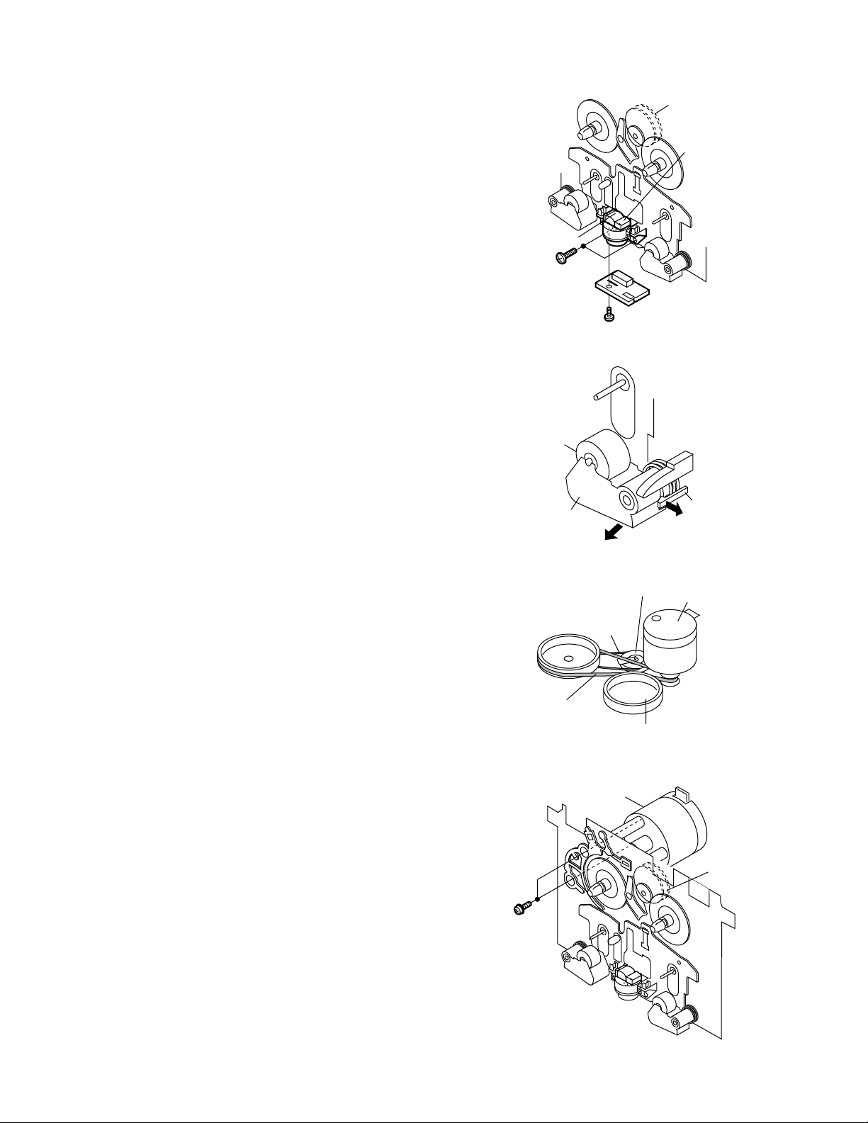
1. TAPE MECHANISM SECTION
Perform steps 1 to 11 of the disassembly method to remove the tape
mechanism.(see page 3-3,3-4)
1.1. How to remove the Record/Playback Head (See Fig. 1)
1. When you remove the screws (A1) x 2 pcs and (A2) x 1 pc., the
record/playback head can be removed.
1.2. How to remove the Pinch Roller (See Fig. 2)
1. Carefully bend the pinch roller pawl in the direction of the arrow
<A>, and remove the pinch roller (B1) x 1 pc., in the direction of the
arrow <B>.
NOTE: When installing the pinch roller, pay attention to the spring
mounting position.
1.3. How to remove the Belt (See Fig. 3)
1. Remove the main belt (C1) x 1 pc., from the motor side.
2. Remove the FF/REW belt (C2) x 1 pc.
1.4. How to remove the Motor (See Fig. 4)
1. Remove the screws (D1) x 2 pcs., to remove the motor.
Erase Head
(A1)x2
Ø2x6mm
Pinch Roller
(B1)x1
Figure 1
Pull
Figure 2
(A2)x1
Ø2x9mm
<B>
Clutch Ass'y
Record/Playback
Head
Pinch
Roller
<A>
Pawl
Main Belt
(C1)x1
(D1)x2
Ø2.6x5mm
FF/REW
Belt
(C2)x1
Figure 3
Motor
Clutch
Flywheel
Motor
Clutch Ass'y
3 – 1
Figure 4
Page 14
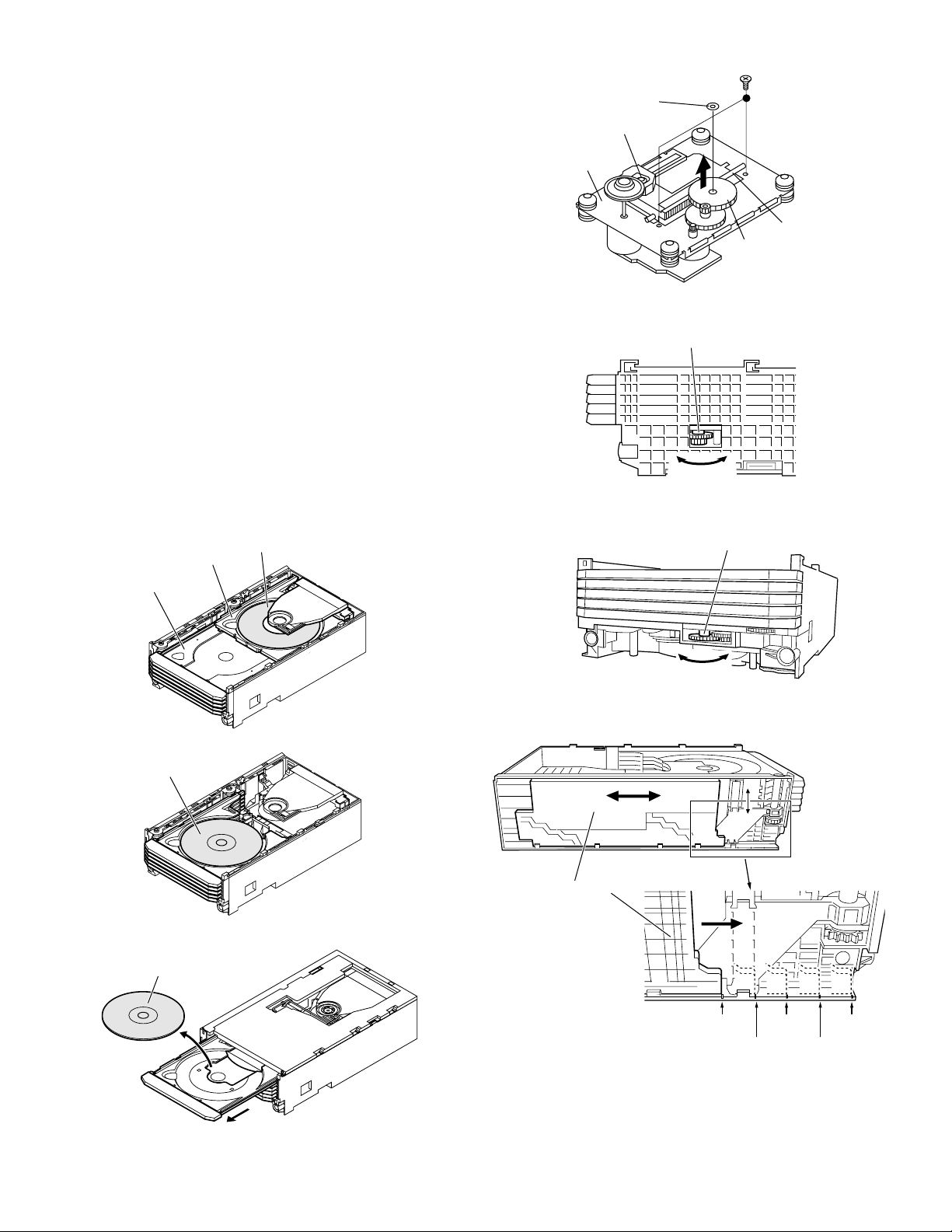
2. CD MECHANISM SECTION
Perform steps 1 to 2 and 14 to 15 of the disassembly method to
remove the CD mechanism.(see page 3-3,3-4)
2.1. How to remove the Optical Pickup (See Fig. 1)
1. Remove the stop washer (A1) x 1 pc and gear (A2) x 1 pc.
2. Remove the screws (A3) x 2 pcs and shaft (A4) x 1 pc.
3. Remove the optical pickup.
NOTE: After pulling out the optical pickup connector, wrap the tip of it
with conductive aluminium foil or the like to protect the optical
pickup from the static electricity.
2.2. How to remove CD Disc (See Fig. 2~6)
1. When CD is at play position, rotate reduction gear C clock-wise as
shown in Figure 2 Until disk tray is at ‘STOCK’ position, then rotate
the gear further to eject the disk tray (Figure 6) so that CD can be
removed from the tray.
2. In another case, if CD mechanism is at tray No. 1 play position and
to remove CD located in tray No. 3, the procedure is as follows:
If the gear up down board is located at tray No. 1 position, then
rotate Reduction gear C clock-wise until Disc tray is at stalk
‘STOCK’ position. Rotate reduction gear D clock-wise (Figure 3) to
move the CD mechanism to tray No. 3 position. This is confirmed
by checking the gear up down board position Base on the marking
as indicated on the main chassis as shown in Figure 4.
• Usually changer is covered with top plate. As for reference purpose, we exclude the top plate for easy viewing. (Figure 5,6)
CD Disc
Disc Tray
Guide Tray
Stop Washer
(A1) x1
Optical Pickup
CD
Mechanism
XL-G5000V/XL-G5000V(S)
(A3) x2
ø2.6 x5mm
Figure 1
Reduction gear C
Front
Rear
Figure 2
Reduction gear D
Gear
(A2) x1
Shaft
(A4) x1
CD Disc
CD Disc
Remove CD from tray.
CD At play position.
CD At 'STOCK' position.
Figure 5
Tray eject
Gear up down board
Up Down
Figure 3
Mark 1
(DISC 1)
Figure 4
Mark 3 Mark 5
(DISC 3)
Mark 2 Mark 4
(DISC 2)
(DISC 4)
(DISC 5)
Figure 6
3 – 2
Page 15
XL-G5000V/XL-G5000V(S)
[2] DISASSEMBLY
Caution on Disassembly
Follow the below-mentioned notes when disassembling the unit and
reassembling it, to keep it safe and ensure excellent performance:
1) Take cassette tape and compact disc out of the unit.
2) Be sure to remove the power supply plug from the wall outlet
before starting to disassemble the unit.
3) Take off nylon bands or wire holders where they need to be
removed when disassembling the unit. After servicing the unit,
be sure to rearrange the leads where they were before disassembling.
4) Take sufficient care on static electricity of integrated circuits and
other circuits when servicing.
STEP REMOVAL PROCEDURE FIGURE
1 Cabinet 1. Screw..........................(A1) x11 1
2 Rear Panel Top 1. Screw............. ...............(B1) x2 1
3 CD Changer unit 1. Hook.............................(C1) x2
4 Rear Panel
Bottom
5 Front Panel 1. Screw...........................(E1) x3
6 Tuner PWB 1. Screw............................(F1) x1
7 Main PWB 1. Screw...........................(G1) x2
8 Power PWB 1. Screw...........................(H1) x4 4
9 Terminal PWB 1. Screw............................(J1) x1 4
10 Display PWB 1. Knob.............................(K1) x1
11 Tape Mechanism 1. Screw...........................(L1) x 4 5
12 Headphones
PWB
13 Mic PWB 1. Knob.............................(N1) x1
14 CD Servo PWB
(Note 1)
15 CD Mechanism 1. Screw...........................(Q1) x3
Note 1:
After removing the connector for the optical pickup from the connector,
wrap the conductive aluminium foil around the front end of the connector so as to protect the optical pickup from electrostatic damage.
2. Socket..........................(C2) x1
3. Flat Cable.....................(C3) x2
1. Screw...........................(D1) x9 2
2,3
2. Flat Cable....................(E2) x2
3. Socket..........................(E3) x2
4. Hook............................(E4) x2
2. Socket..........................(F2) x1
2,4
2. Socket.........................(G2) x4
2. Screw...........................(K2) x 8
3. Flat Cable....................(K3) x 1
1. Screw..........................(M1) x 1 5
2. Screw..........................(N2) x 1
1. Screw...........................(P1) x3
2. Flat Cable...................(P2) x 2
3. Socket..........................(P3) x1
2. Screw...........................(Q2) x4
Cabinet
(A1) x1
ø3x8mm
Rear
Panel Top
(A1) x1
ø3x8mm
(A1) x2
ø3x8mm
(B1) x2
ø3x10mm
(A1) x2
ø3x8mm
(A1) x2
2
ø3x8mm
Rear
Panel
Bottom
Front Panel
(A1) x1
ø3x10mm
(A1) x2
ø3x8mm
Figure 1
CD Servo PWB
3
2
3
CD Changer
Unit
(C3) x2
(C2) x1
Front Panel
4
Pull
Hook
5
Rear
Panel Bottom
(C1)x1
Hook
(C1)x1
Pull
Main PWB
Headphones
PWB
5
(D1) x9
6
6
7
ø3x8mm
Tape
Mechanism
(E3) x1
Figure 2
(E2) x1
(G1) x1
ø3x10mm
(F1) x1
ø3x8mm
(F2) x1
(E2) x1
(E1) x1
ø3x10mm
3 – 3
Front Panel
MIC PWB
(E3) x1
Hook
(E4)x1
Pull
(612) x1
ø3x6mm
Hook
(E4)x1
(E1) x2
ø3x10mm
Pull
Figure 3
Turner PWB
Main PWB
Page 16
XL-G5000V/XL-G5000V(S)
(G2) x2
Power PWB
(K1) x1
Cassette
Holder
(N1) x1
Main PWB
(H1) x4
ø4x6mm
Display PWB
Front Panel
(G1) x1
ø3x6mm
Figure 4
(G2) x2
Terminal PWB
(K3) x1
(K2) x8
ø2.6x8mm
Tape
Mechanism
Headphones
PWB
(J1) x1
ø3x6mm
(Q2) x4
ø2.6x10mm
CD Mechanism
CD Changer
Unit
Figure 7
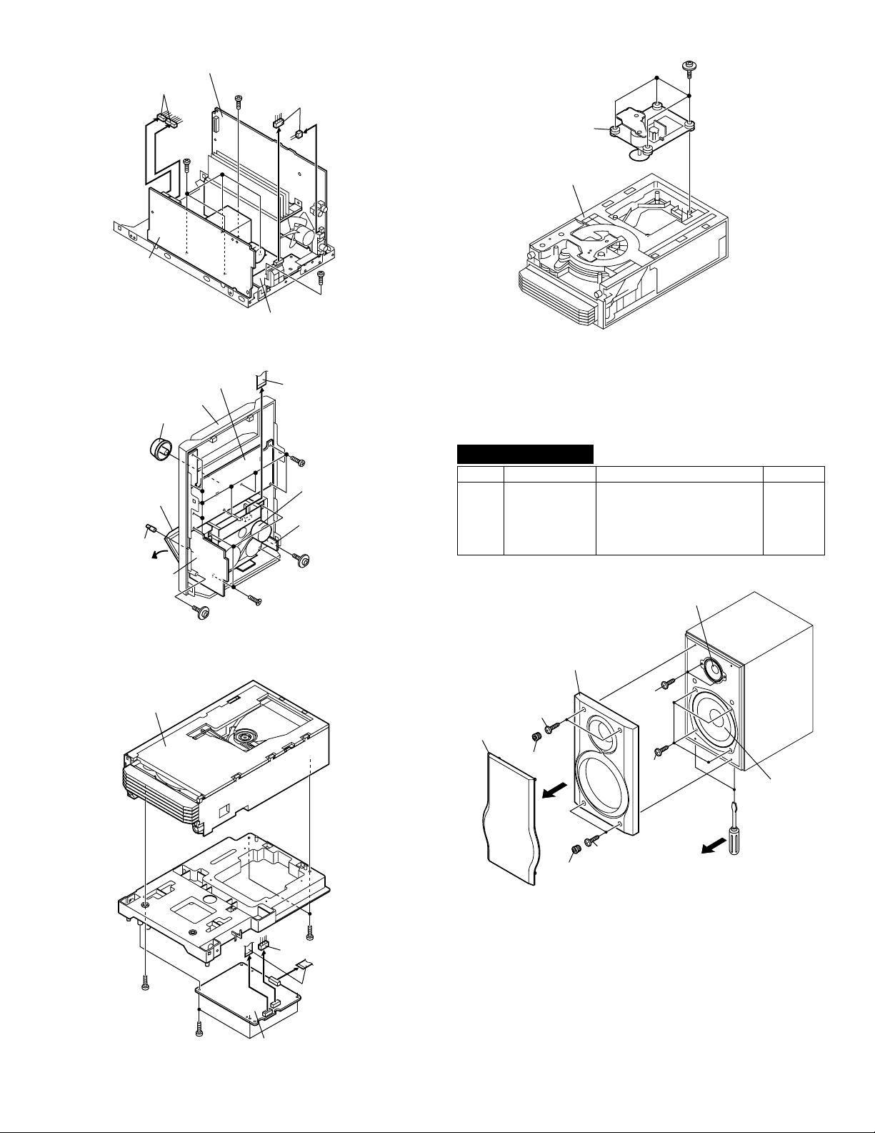
FRONT SPEAKER
STEP REMOVAL PROCEDURE FIGURE
1Woofer/
Tweeter
1. Net Frame................(A1) x1
2. Catching Holder.......(A2) x4
3. Screw.......................(A3) x4
4. Front Panel..............(A4) x1
5. Screw.......................(A5) x6
8
MIC PWB
CD Changer
Unit
(N2) x1
ø3x10mm
Figure 5
(L1) x4
ø3x10mm
(M1) x1
ø3x10mm
(P3) x1
(Q1) x2
ø3x10mm
Net Frame
(A1)x1
Front Panel
(A4)x1
(A3)x2
ø3.5x16mm
(A2)x2
(A2)x2
(A5)x2
ø3.5x14mm
(A3)x2
ø3.5x16mm
Figure 8
Tweeter
(A5)x4
ø3.5x14mm
Woofer
Screwdriver
(Q1) x1
ø3x10mm
(P1) x3
ø3x10mm
Figure 6
(P2) x2
CD Servo PWB
3 – 4
Page 17
XL-G5000V/XL-G5000V(S)
SURROUND SPEAKER
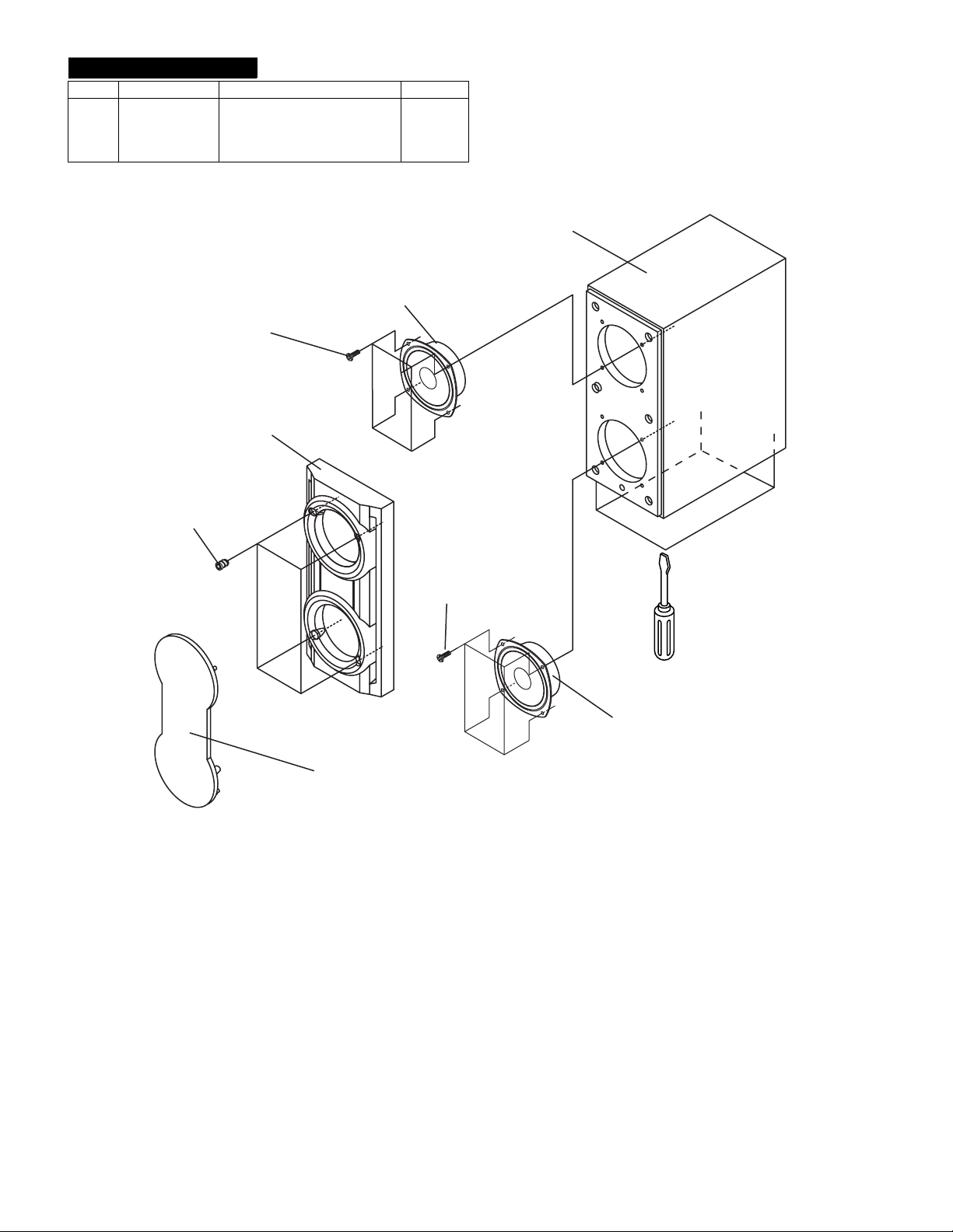
STEP REMOVAL PROCEDURE FIGURE
1 Fullrange
Speaker
1. Net Frame................(A1) x1
2. Catching Holder.......(A2) x4
3. Front Panel..............(A3) x1
4. Screw.......................(A4) x8
Full range speaker
(A4) x 4
ø3.5x14mm
Front panel
(A3) x 1
9
Speaker Box Assy
Catching Holder
(A2) x 4
(A4) x 4
ø3.5x14mm
Screwdriver
Full range speaker
Net frame
(A1) x 1
Figure 9
3 – 5
Page 18
XL-G5000V/XL-G5000V(S)
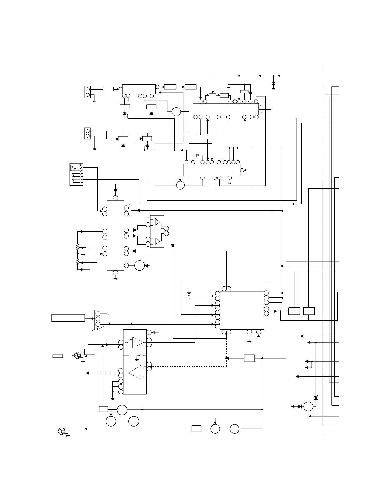
CHAPTER 4. DIAGRAMS
[1] BLOCK DIAGRAM
FM ANTENNA
AM LOOP
ANTENNA
JK1/2
MIC JACK
VRK1
MIC LEVEL
FROM VCD SECTION
CNP6
REC /P.B. HEAD
L-CH
TAPE
R-CH
AC BIAS
TERMINAL
SO302
CNP301
2
1
MIC IN
MIC1OUT
MIC2OUT
SWITCHING
Q101Q104
CNS6
1
2
3
B.P.F
BF301
12
13
1
FM RF
AM
TRACKING
T303 T306
40
LATCH
DATA
4
CLOCK
9
ROUT
7
LOUT
8
RIN
LIN
VCC
22
ICK1
M65856SP
MIC AMP.
L(TA)
2
23
R(TA)
LREC
9
16
RREC
11
12
15
FM FRONT END
384
L312 T301
42
41
35
36
32
31
23
REC
IC301
TA7358AP
7
5
FM OSC
AM BAND
COVERAGE
+B5
QK1
P.B
H/N
FM IF
R
L
OSC
BUFF
Q302
CF303T302
VT
20 22 11171615
+B5
FM
Q360
ICK2
TJM4558CD
4.5 MHZ
OPE AMP.
6
9
PLL(TUNER)
FM+B
SWITCHING
6
5
2
3
IC302
LC72131
7
1
+B5
JK690
L
R
+B5
13
4
L
PB
21
R
L
REC
7
18
R
IC101
AN7345K
PLAYBACK AND RECORD
/PLAYBACK AMP.
21
AM OSC IN
AM OSC OUT
X352
OSC
7
VIDEO/AUX
TAPE
TUNER
CD
AM MIX
T351
CF352
AM IF
OUT
21
7
STEREO
AM RF IN
CE
MO/ST
FM/AM
9
10
8
L
9
R
16
L
10
15
R
L
11
AUDIO PROCESSOR
14
R
L
12
R
13
718
4
98517
GND
AM IF
FM/AM
OUT
18
CLK
DO
DI
5413
6
21
17
IC601
LC75341
10.7 MHz
CF351
FM
DET
VCC
MPXIN
162324
+B5
3
Q107
Q108
MUTING
456 kHz
VCO
FM/AM
12
13
20
ZD351
5.1V
X351
FM MPX./AM IF
14
L
MO/ST
R
15
DI
1
CE
2
CLK
24
R
21
L
4
23
+B5
REC/PLAY
+B5
IC303
LA1832S
FM IF DET.
–20dB
ATT
Q601
Q602 Q604
+B7(A_+5V)
+B8(D_+5V)
+B9(SW_+5V)
+B5
+B4
Q603
LD_+8.5V
A_+10V
MUTE
SYSTEM
ERASE
HEAD
SWITCHING
Q105
Q106
Q112
Q114
+B5
SWITCHING
SWITCHING
Q113
BIAS
OSC
Figure 4-1 BLOCK DIAGRAM (1/3)
4 – 1
Q111
L103
+B5
Q109
SWITCHING
BIAS
Q110
BIAS
+B_PROTECT
Q860
+B10
Page 19
B
1
7
Y
N
R
S
A
L
603
604
D_+8V
)
10V
851
0
MUTE
SYSTEM
+B10
+B5
IC851
AN80T53
MULTI
REGULATOR
GND
5.1V
8.5V
10V
REGULATOR
VF2
–VF
VF1
UNSW_5.6V
P_IN
LED701
Q711
LED708
LED707
SW
VCC
IC852
KIA7805AP
VOLTAGE
AC_RLY
Q719
PHOTO
TO VCD SECTION
Q710
18
L
R
14
13V
235671 4
+B3
IC854
AN78L05
VOLTAGE
REGULATOR
NC
SP DET
IC901
STK432-070
POWER AMP.
VH+
GND
VL-
1
VL+
7
5
2
D801
–B2
+B2
D802
VOLTAGE
REGULATOR
XL-G5000V/XL-G5000V(S)
FL701
FL DISPLAY
5
2121 4445
PHOTO
VH-
6
Q801
6
8
3837 46
48
KARA_LATCH
60
MIC_SW
59
5
DSA_STB
DSA_DATA
8
DSA_ACK
9
62
MOT_A+
MOT_A-
MPEG_PWR
66
49
52
VLOAD
79
P_IN
36
SMUTE
41
TIME LED
42
VOL_LED
45
ILLU_LED
58
80
83
84
100
VDD
-20dBATT
12 16
+B10
L-OUT
R-OUT
F802
T4.0A L 250V
F801
T4.0A L 250V
F804
T2A L 250V
F803
T2A L 250V
AC_RLY
MOT_B+
MOT_B-
SYSTEM MICROCOMPUTER
T_REC/PLAY
T_BIAS
XL700
4.19403MHz
Q901
Q904
+B10
4443
VDD
T_SOL
T_MOTOR
IC701
IXA034AW
VDD
+B10
Q905
TRANSFORMER
T.F
32 413128
242115121176
PT801
POWER
(MAIN)
110V
69
TUN_SM/SPAN
CLKDIDO
17 18 19 2034
RL914
RELAY
230-240V
220V
127V
LIFE
NEUTRAL
78
REMOCON
AVDD
VOL_JOG
PROTECT
RESET
SP_RLY
CE
DRIVER
Q906
+B3
SW801
VOLTAGE
SELECTOR
CNP805
3
22
131
MOTOR/
SOLENOID
DRIVER
Q701,702
Q712~715
+B3
27
13
25
40
39
34
33
31
30
29
10
56
53
47
HEADPHONES
BROWN
BLUE
SUPPLY CORD
AC 110/127/220/
230-240V,50/60Hz
+B_PROTECT
FAN MOTOR
M971
M
SO901
SPEAKER TERMINAL
JK701
JK953
SUB WOOFER
PRE-OUT
AC POWER
REMOTE SENSO
RX701
1
+B10
KEY
SW701-SW72
KEY
SW722-SW72
VOLUME
VR701
Q703
RESET
TO VCD
+B7(A_5V)
MECHA
ASS'
3
+B10
TAP
SW
SP
SE
2
+
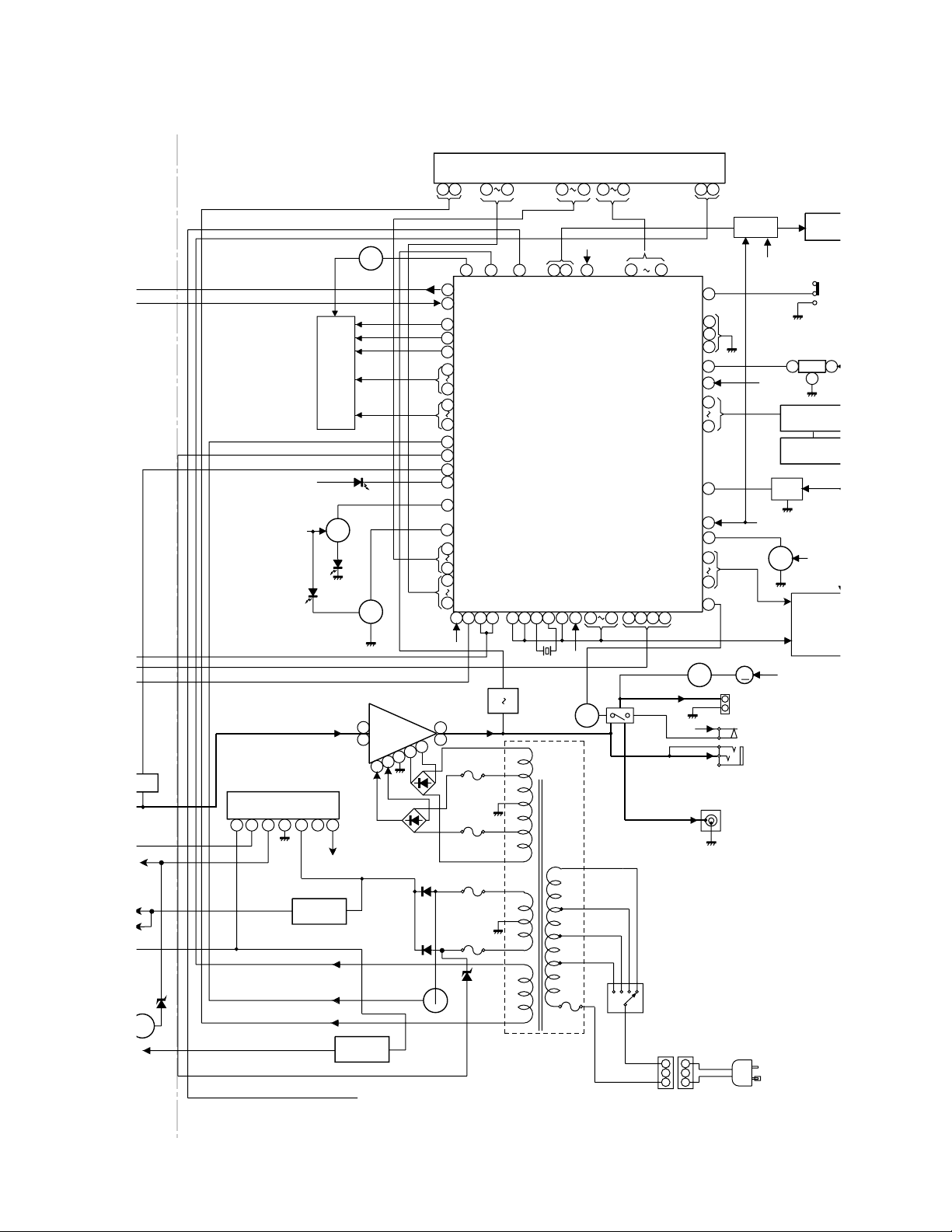
Figure 4-2 BLOCK DIAGRAM (2/3)
4 – 2
Page 20
XL-G5000V/XL-G5000V(S)
PAL/NTSC
LA17
LA0
~
DGND
+B7
32165
VCC
AUX4
69
DSC_D1
DSC_D0
55
LD0
~
62
LD7
LROMCE
65
64
LOE
68
LA0
~~
79
LA11
LA12
82
LA17
87
~~
~
ES3889F
RSTOUT
6
24
66
29
RESET
ICM3
DSC_C
10
53
LCSI
TDMDR
97
MCLK
17
19
TWS/SPLLOUT
TSO
21
22
TSCK
13
RST
RWS/SPLL1
RSD/SPLL0
RSCK_SER_IN
23 33 37
AJN
ARFS
ARCLK
32
1
2
13
~
12
23
25
~
30
16
ICM4
EPROM
IX0528AW
~~
15
17
21
22
24
VIDEO-ENCODER/AUDIO DAC
DSC_D4
DSC_D3
DSC_D2
DSC_D7
DSC_D6
DSC_D5
VGND
5756 62 63
VSS
DSC_5
13125 26 72 75 77 9181 9383 85 95 97 99 8
MCLK
TSO
TSCK
88 89 9091 93 94 95
ACLK
AUX5
ATCLK
AOUT/SEL_PLL0
TDMCLK
AUX4
TDMFS
49
98 54 48 47
96
6459 60534490787366
VDAC
PCK
100
79
80
DGND
TWS
44
43
AJN
PCLA
ARFS
ARCLK
ATFG/SEL_PLL1
ICM2
ES3880FM
MPEG-DECODER
AUX7
AUX3
AUX2
AUX6
AUX0
AUX1
4546
52
AOL+
AOL–
AOR–
AOR+
PCK2
HSYNC
82
84
41
40 39 32
HSYNC
PCLA2X
VSYNC
VSYNC
+B5
QM1
48
2
IC3
L
47
3
~
YUV7
TJM4558CD
5
OPE. AMP.
6
AGND
+B5
~
51311
VCC3
~
VCC
YUV0
DBUS0
~
DBUS15
DWE
RAS
MA0
~
MA8
CAS
DOE
92
99
46
45
41
43
51
86
89
92
94
96
98
7
1
R
84
AGNDA
+B8
QM2
QM3
QM4
81
13
~
28
3
2
4
~
12
JK690
VIDEO OUT
2
~
5
7
~
10
13
ICM1
14
16
~
19
21 35 40
2061
39
~~~
36
34
31
29
28
D-RAM
4M/16M
27
LC1625635T
26
22
DGND
PICKUP UNIT
TR+
FO+
FO–
TR–
M1A
SPINDLE
MOTOR
M2A
SLED
MOTOR
SW1A
PICKUP-IN
MPEG POW
DSA_ACK
DSA_DATA
ESS_STB
DSA_STB
ESS_ACK
ESS_DO
ESS_DI
(+B5)
(+B4)
(+B8)
(+B9)
SW3
TRAY SW2
SW2
TRAY SW1
SW4
DISC
RX1
PHOTO
INTERRUPTER
M
TRAY
MOTOR
M
MAIN CAM
M1
M2
MOTOR
TO DISPLAY SECTION
TO MAIN SECTION
FROM DISPLAY SECTION
GND
D_GND
5556576977585960 51 50 44 43 40 2837 17 6
PAL/NTSC
SLDO
SPDO
XOUT
VDD5
*WRQ
*RES
MON13
XIN
DO
DRF
72
CE
CL
DI
CONT1
27
49
XL1
48
16.9344 MHz
68
61
62
63
64
65
66
67
+B
+B4
+B8
Q3
Q4
34
MOT_B+
MOT_B–
1
MOT_A+
MOT_A–
2
3
4
5
6
7
8
9
10
11
D_GND
TRAY_SW2
TRAY_SW1
CLAMP
DISC
PHOTO
+5V
TR+
TR–
CAM+
CAM–
CNP4 CNB1
VCC
E
A
B
F
C
VREF
FO–
TR–
+B8
TR+
FO+
D_GND
LASER
DRIVER
Q1
L1
0.82µH
A
+5V
30 26725 27928
GND
1
VO3+
VO3–
2
VO4+
+
M
M
6
–
5
+
4
3
–
2
1
CNP3
D_GND
35
VO4–
36
3
VO2+
VO2–
4
VO1+
5
VO1–
6
+5V
Q2
+B8
DATA
LRSY
DATACK
10
VREF
LDD
19
LDS
20
XVDD
47
RVDD
46
LVDD
41
AVDD1
7
AVDD2
18
VDD
38
DIGITAL SIGNAL PROCESSOR
VVDD
75
AIN
2
CIN
3
BIN
4
DIN
5
EIN
12
FIN
13
MPEG_RESET
2625 21 22 23 24
+B8
+5V
SVCC
SGND
PGND1
PGND2
PVCC1
VREFIN
VO6+
VO6–
VO5+
VO5–
34 33810 3231 2421
A
+5V
IC1
LC78637E
/PUIN SW
CONT5
+B4
VCONT6
IC2
LA6261
FOCUS/TRACKING/
+8V
SPIN/SLED DRIVER
PVCC2
CD
FWD6
REV6
VCONT5
VIN1
VIN2
VIN3
VIN4
FWD5
REV5
FDO
TDO
11
13
15
17
22
23
19
20
CNP6
CNP5
1
2
3
4
5
6
7
8
9
10
11
1
2
3
4
5
6
7
8
1
2
3
4
5
6
7
8
9
10
11
12
13
14
R-CH
AGND
L-CH
DGND
A_+10V
D_GND
+8V
A_+5V
CD_RESOUT
WRQ
DRF
DO
DI
CL
CE
DISC
CLAMP
TRAY_SW1
TRAY_SW2
PHOTO
D_GND
+5V
SW1
CLAMP
+
–
+
–
D1
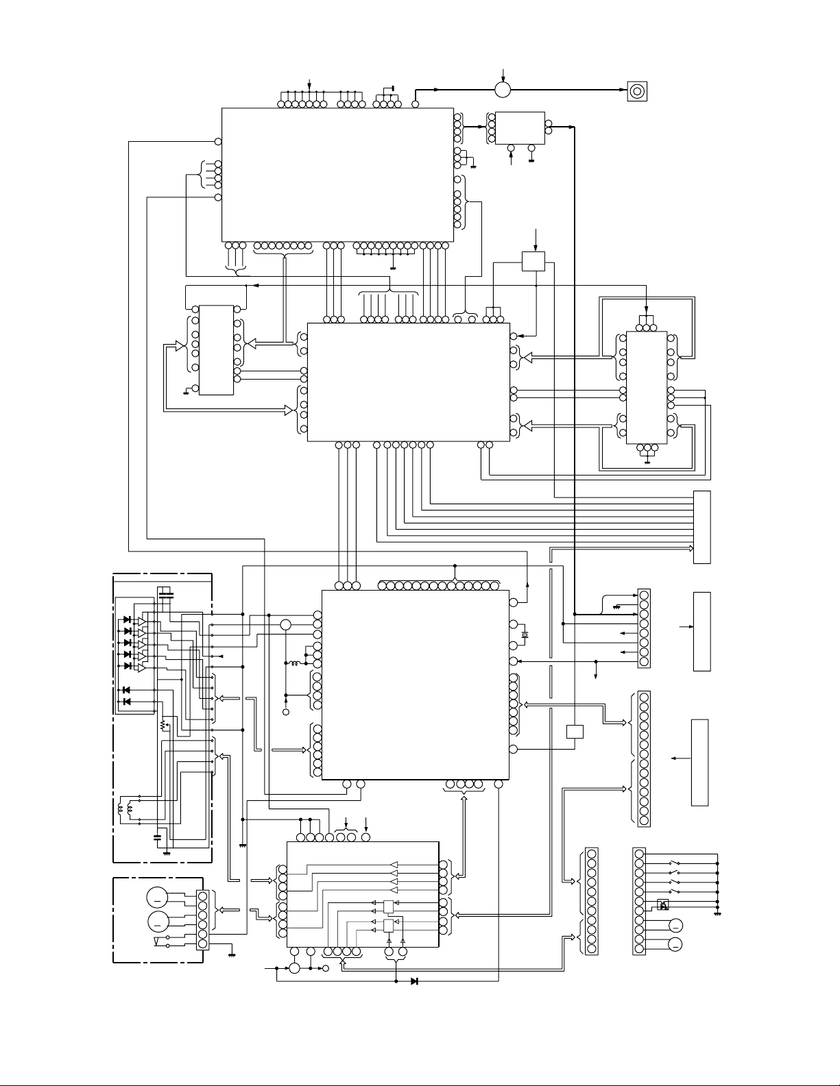
Figure 4-3 BLOCK DIAGRAM (3/3)
4 – 3
Page 21
AudioXL-G5000VService ManualXL-G5000V(S)MarketE
CHAPTER 5. CIRCUIT DESCRIPTION
XL-G5000V/XL-G5000V(S)
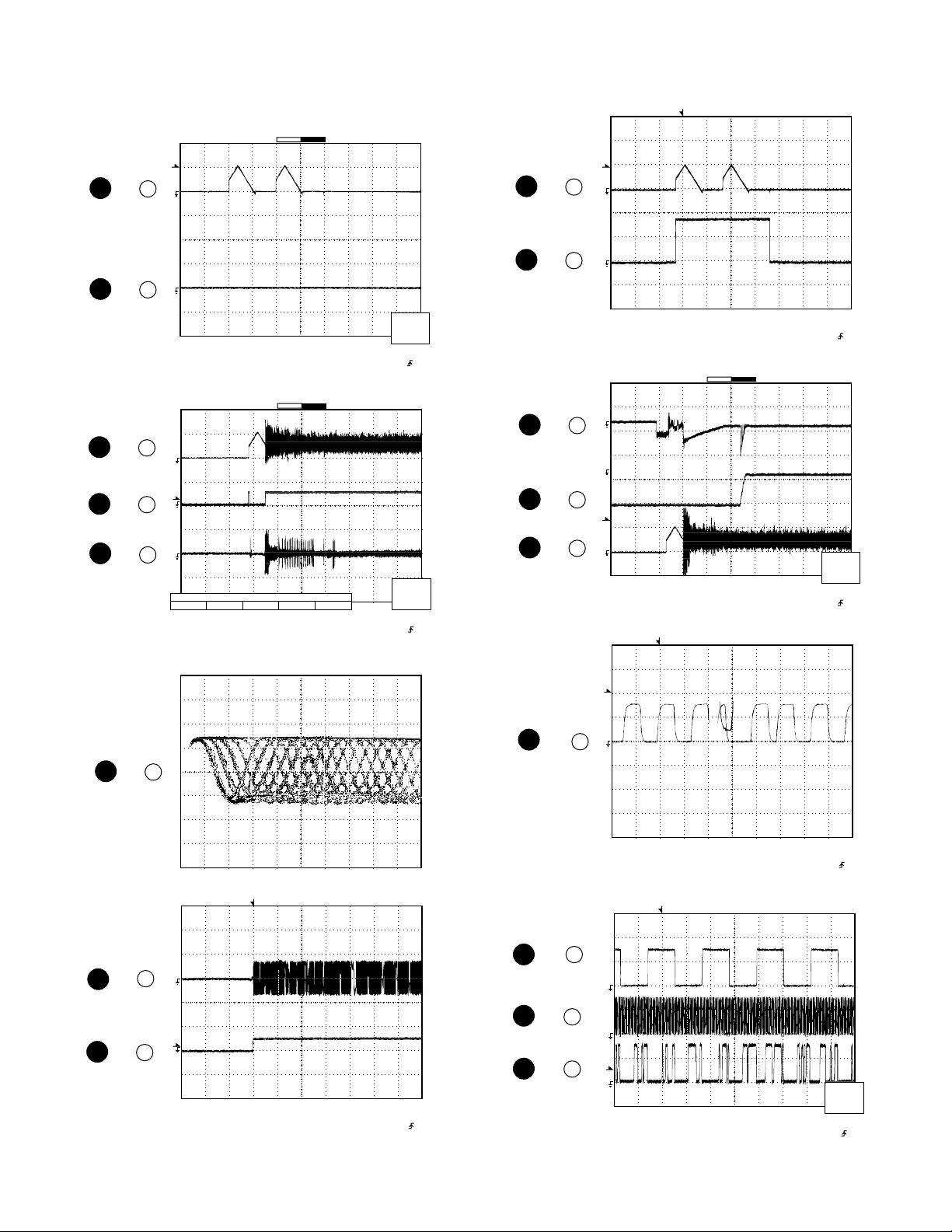
[1] WAVEFORMS OF CD CIRCUIT
Stopped
1
2
1
3
4
IC1 21
IC1 22
IC1 21
IC1 67
IC1 15
CH1=500 mV
DC 10:1
T
FDO
1
TDO
3
Smoothing : ON CH1 : 0.000 V
BW : FULL
Stopped
1
T
2
3
-3 div -1 div 0 div +1 div +3 div
Smoothing : ON CH1 : 0.000 V
BW : FULL
CH1=500 mV
DC 10:1
FDO
DRF
TE
CH2 : 0.0 V
CH3 : 0.000 V
CH4 : 0.00 V
CH2=10 V
DC 10:1
CH Position To
CH2 : 0.0 V
CH3 : 0.00 V
CH4 : 0.00 V
CH3=500 mV
DC 10:1
=Record Length=
Main : 100 K
Zoom : 2 K
CH3=1 V
DC 10:1
=Record Length=
Main : 100 K
Zoom : 2 K
Mode : AUTO
Type : EDGE CH1
Delay : 0.0 ns
Hold off : 0.2 µs
Mode : AUTO
Type : EDGE CH1
Delay : 0.0 ns
Hold off : 0.2 µs
500 ms/div
(500 ms/div)
NORM:20 kS/s
=Trigger==Filter= =Offset=
500 ms/div
(500 ms/div)
NORM:20 kS/s
=Trigger==Filter= =Offset=
CH1
v/DIV
500 mV
CH2
Position
0.20 div
1
6
7
8
1
IC 1 21
IC 1 24
IC1 73
IC1 74
IC1 21
Stopped
CH1=200 mV
DC 10:1
T
FDO
2
SPDO
1
Smoothing : ON C H1 : 0.000 V
BW : FULL
Stopped
CH1=500 mV
DC 10:1
PDO1
3
4
PDO2
T
FDO
1
Smoothing : ON CH1 : 0.000 V
BW : FULL
Stopped
CH1=2 V
DC 10:1
T
T
CH2=500 mV
DC 10:1
CH2 : 0.000 V
CH3 : 0.00 V
CH4 : 0.00 V
CH2 : 0.0 V
CH3 : 0.00 V
CH4 : 0.00 V
T
=R ec or d Leng th=
Main : 100 K
Zoom : 2 K
CH3=1 V
DC 10:1
=Record Length=
Main : 100 K
Zoom : 2 K
1999/04/07 09:51: 15
500 ms /div
(500 ms /div)
NORM: 20 kS/s
=Trigger==Filter= =Offs e t=
Mode : N O R MAL
Type : E DGE CH2
Delay : 2.924 ms
Hold off : 0.2µs
1999/04/05 17:33:17
CH4=1 V
500 ms/div
(500 ms/div)
DC 10:1
NORM:20 kS/s
=Trigger==Filter= =Offset=
Mode : AUTO
Type : EDGE CH2
Delay : 0.0 ns
Hold off : 0.2 µs
1999/04/07 09:25:28
500 ns/div
(500 ns/div)
NORM:200 MS/s
CH1
v/DIV
500 mV
4
3
5
IC1 80
IC1 15
IC1 67
Stopped
CH1=10 V
DC 10:1
TE
2
DRF
T
1
=Filter= =Offset=
Smoothing : ON CH1 : 0.0 V
BW : FULL
T
CH2=1 V
DC 10:1
CH2 : 0.00 V
CH3 : 0.00 V
CH4 : 0.00 V
=Record Length=
Main : 100 K
Zoom : 2 K
Vp-p=1.0 V~1.3 V
0.5 mV/div,0.5 µsec/div
100 ms/div
(100 ms/div)
NORM:100 kS/s
=Trigger=
Mode : NORMAL
Type : EDGE CH1
Delay : 2.924ms
Hold off : 0.2 µs
10
11
12
9
IC1 39
IC1 58
IC1 59
IC1 60
1
DOUT
Smoothing : ON CH1 : 0.00 V
BW : FULL
1
2
T
3
Smoothing : ON CH1 : 0.00 V
BW : FULL
Stopped
LRSY
DATACK
DATA
CH1=2 V
DC 10:1
CH2 : 0.00 V
CH3 : 0.00 V
CH4 : 0.00 V
T
CH2=2 V
DC 10:1
CH2 : 0.00 V
CH3 : 0.00 V
CH4 : 0.00 V
=Record Length=
Main : 1 K
Zoom : 100
CH3=2 V
DC 10:1
=Record Length=
Main : 5 K
Zoom : 100
=Trigger==Filter= =Offset=
Mode : NORMAL
Type : EDGE CH1
Delay : 2.887ms
Hold off : 0.2 µs
1999/04/05 20:50:17
5 µs/div
(5 µs/div)
NORM:100 kS/s
CH3
v/DIV
=Trigger==Filter= =Offset=
Mode : AUTO
Type : EDGE CH3
Delay : 0.0 ns
Hold off : 0.2 µs
2V
5 – 1
Page 22
XL-G5000V/XL-G5000V(S)
[2] VOLTAGE
PIN
NO.
1
2
3
4
5
6
7
8
9
10
11
12
13
14
15
16
17
18
19
20
21
22
23
24
25
26
27
28
29
30
31
32
33
34
35
36
37
38
39
40
41
42
43
44
45
46
47
48
49
50
51
52
53
54
55
56
57
58
59
60
61
62
63
64
65
66
67
68
69
70
71
72
73
74
75
76
77
78
79
80
IC1
VOLTAGE
1.65 V
1.65V
1.65 V
1.65 V
1.65 V
0.00 V
3.28 V
1.67 V
0.50 V
1.67 V
0.40 V
1.67 V
1.67 V
1.67 V
1.67 V
1.67 V
0.00 V
3.28 V
3.28 V
0.00 V
1.67 V
1.67 V
1.67 V
1.67 V
3.28 V
3.28 V
0.00 V
0.00 V
0.00 V
3.25 V
0.00 V
0.00 V
0.00 V
0.00 V
0.00 V
0.00 V
0.00 V
3.25 V
0.00 V
0.00 V
3.25 V
1.65 V
0.00 V
0.00 V
1.65 V
3.25 V
3.25 V
1.62 V
1.62 V
0.00 V
0.00 V
3.22 V
1.28 V
0.00 V
0.00 V
0.00 V
0.00 V
1.63 V
1.60 V
1.12 V
0.00 V
4.69 V
0.00 V
5.03 V
5.11 V
4.73 V
0.00 V
5.11 V
0.00 V
0.00 V
0.00 V
0.00 V
1.30 V
0.60 V
3.28 V
1.10 V
0.00 V
1.61 V
1.61 V
1.68 V
PIN
NO.
PIN
NO.
1
2
3
4
5
6
7
8
9
10
11
12
13
14
15
16
17
18
19
20
21
22
23
24
25
26
27
28
29
30
31
32
33
34
35
36
37
38
39
40
1
2
3
4
5
6
7
8
ICM1
VOLTAGE
5.00 V
1.90V
1.90 V
2.00 V
1.80 V
5.01 V
1.90 V
2.40 V
2.20 V
3.70 V
0.00 V
0.00 V
4.95 V
4.28 V
0.00 V
2.40 V
2.40 V
2.66 V
2.21 V
5.00 V
0.00 V
2.26 V
2.35 V
2.00 V
2.90 V
2.40 V
0.00 V
4.53 V
4.53 V
0.00 V
2.50 V
2.50 V
2.50 V
2.50 V
0.00 V
2.50 V
0.00 V
2.60 V
3.40 V
0.00 V
IC3
VOLTAGE
5.04 V
4.20 V
4.20 V
0.00 V
4.20 V
4.20 V
5.04 V
9.92 V
PIN
NO.
10
11
12
13
14
15
16
17
18
19
20
21
22
23
24
25
26
27
28
29
30
31
32
33
34
35
36
37
38
39
40
41
42
PIN
NO.
1
2
3
4
5
6
7
8
9
1
2
3
4
5
6
7
8
ICK1
VOLTAGE
1.66 V
1.84V
1.58 V
3.31 V
3.31 V
3.31 V
3.31 V
3.31 V
3.31 V
3.31 V
3.31 V
3.31 V
3.31 V
3.31 V
3.31 V
3.31 V
3.31 V
3.31 V
3.31 V
1.53 V
3.31 V
0.84 V
5.74 V
0.40 V
3.31 V
3.31 V
3.31 V
3.31 V
3.31 V
3.27 V
3.31 V
3.31 V
3.26 V
3.31 V
3.31 V
3.31 V
3.31 V
1.11 V
0.00 V
0.00 V
0.00 V
0.00 V
ICK2
VOLTAGE
4.91 V
5.70 V
5.70 V
0.84 V
5.68 V
5.68 V
5.68 V
9.69 V
PIN
NO.
PIN
NO.
1
2
3
4
5
6
7
8
9
10
11
12
13
14
15
16
17
18
19
20
21
22
23
24
25
26
27
28
29
30
31
32
33
34
35
36
1
2
3
4
5
6
7
8
9
10
11
12
13
14
15
16
17
18
19
20
21
22
23
24
IC2
VOLTAGE
2.16 V
2.16 V
2.16 V
2.16 V
2.16 V
2.16 V
0.00 V
4.31 V
4.98 V
3.28 V
1.67 V
1.67 V
1.67 V
1.67 V
1.67 V
1.67 V
4.25 V
4.25 V
4.25 V
4.25 V
2.49 V
4.25 V
4.25 V
2.27 V
1.67 V
0.00 V
4.97 V
8.43 V
4.97 V
0.00 V
0.00 V
0.00 V
0.00 V
0.00 V
2.16 V
2.16 V
IC101
VOLTAGE
0.00 V
0.00 V
0.60 V
2.00 V
2.86 V
0.00 V
0.00 V
0.60 V
3.35 V
3.27 V
0.00 V
0.00 V
6.78 V
4.07 V
0.00 V
3.32 V
0.60 V
0.00 V
0.00 V
2.85 V
1.98 V
0.60 V
0.00 V
0.00 V
PIN
NO.
PIN
NO.
PIN
NO.
10
11
12
13
14
15
16
17
18
19
20
21
22
10
11
12
13
14
15
16
17
18
19
20
21
22
23
24
IC301
1
2
3
4
5
6
7
8
9
IC302
1
2
3
4
5
6
7
8
9
IC303
1
2
3
4
5
6
7
8
9
VOLTAGE
0.00 V
0.00 V
0.00 V
0.00 V
0.00 V
0.00 V
0.00 V
0.00 V
0.00 V
VOLTAGE
2.49 V
0.00 V
0.00 V
0.00 V
0.00 V
5.13 V
9.87 V
4.65 V
0.00 V
0.00 V
5.03 V
0.00 V
5.03 V
0.00 V
0.00 V
2.49 V
5.13 V
0.00 V
0.00 V
9.89 V
0.00 V
2.57 V
VOLTAGE
2.11 V
5.03 V
2.11 V
2.11 V
0.00 V
4.98 V
4.98 V
3.33 V
5.03 V
4.30 V
1.78 V
1.24 V
2.28 V
1.29 V
1.26 V
2.07 V
0.32 V
1.42 V
2.04 V
1.43 V
2.08 V
2.08 V
5.02 V
3.52 V
PIN
NO.
10
11
12
13
14
15
16
17
18
19
20
21
22
23
24
PIN
NO.
PIN
NO.
PIN
NO.
1
2
3
4
5
6
7
8
9
1
2
3
4
5
6
7
1
2
3
1
2
3
IC601
VOLTAGE
0.00 V
0.00 V
0.00 V
4.96 V
4.87 V
4.87 V
4.87 V
4.96 V
4.89 V
4.89 V
4.89 V
4.89 V
4.89 V
4.89 V
4.89 V
4.89 V
4.96 V
4.87 V
4.87 V
4.87 V
4.96 V
4.94 V
9.93 V
0.00 V
IC851
VOLTAGE
5.04 V
12.84 V
20.50 V
0.00 V
19.50 V
9.95 V
8.43 V
IC852
VOLTAGE
20.50 V
0.00 V
5.15 V
IC854
VOLTAGE
5.72 V
0.60 V
9.96 V
PIN
NO.
PIN
NO.
1
2
3
4
5
6
7
8
9
10
11
12
13
14
15
16
17
18
19
20
21
22
23
24
25
26
27
28
29
30
31
32
33
34
35
36
37
38
39
40
41
42
43
44
45
46
47
48
49
50
1
2
3
4
5
6
7
8
9
10
11
12
13
14
15
16
17
18
19
20
21
22
23
24
25
26
27
28
29
30
31
32
33
34
35
36
37
38
39
40
41
42
43
44
45
46
47
48
49
50
VOLTAGE
4.77V
4.65V
0.01V
4.74V
5.06V
4.76V
1.00V
5.06V
5.06V
4.88V
2.30V
2.04V
0.01V
3.44V
0.00V
4.80V
0.02V
0.02V
5.09V
0.02V
0.02V
0.09V
0.06V
0.80V
0.01V
5.06V
4.35V
5.08V
5.06V
-0.02V
5.06V
5.06V
5.06V
4.77V
5.06V
1.88V
5.06V
5.08V
4.94V
0.01V
4.50V
3.86V
13.00V
13.00V
0.04V
4.80V
4.56V
4.75V
3.95V
0.00V
VOLTAGE
0.07V
1.54V
1.56V
1.56V
1.56V
1.56V
1.56V
1.56V
1.56V
1.56V
1.56V
1.56V
1.56V
1.56V
1.56V
1.56V
1.57V
1.57V
1.57V
1.57V
1.57V
1.57V
1.57V
1.57V
1.57V
1.57V
1.57V
1.57V
1.57V
0.02V
0.07V
1.58V
1.58V
1.58V
1.58V
1.58V
1.58V
1.58V
1.58V
1.58V
1.58V
1.58V
1.58V
0.19V
2.02V
1.66V
0.02V
1.66V
1.58V
0.02V
IC701
ICM2
PIN
NO.
100
PIN
NO.
100
51
52
53
54
55
56
57
58
59
60
61
62
63
64
65
66
67
68
69
70
71
72
73
74
75
76
77
78
79
80
81
82
83
84
85
86
87
88
89
90
91
92
93
94
95
96
97
98
99
51
52
53
54
55
56
57
58
59
60
61
62
63
64
65
66
67
68
69
70
71
72
73
74
75
76
77
78
79
80
81
82
83
84
85
86
87
88
89
90
91
92
93
94
95
96
97
98
99
VOLTAGE
0.00V
4.77V
5.06V
5.06V
5.06V
5.06V
-28.40V
4.75V
0.01V
0.01V
0.04V
4.75V
4.75V
0.01V
0.01V
4.74V
4.78V
4.76V
-28.00V
-28.00V
-28.45V
-26.00V
-28.01V
-15.97V
-23.22V
-18.39V
-26.37V
-22.30V
-28.50V
-27.00V
-20.00V
-26.13V
-25.57V
-25.55V
-25.55V
-25.56V
-11.06V
-0.09V
-25.57V
-25.60V
-25.63V
-25.61V
-25.60V
-25.56V
-25.58V
-25.57V
-25.55V
-25.55V
-25.52V
-26.00V
VOLTAGE
0.07V
1.58V
1.58V
1.65V
1.58V
1.58V
1.58V
1.58V
1.58V
1.58V
1.57V
1.57V
1.57V
1.57V
1.57V
1.57V
1.57V
1.57V
1.57V
1.57V
1.57V
1.57V
1.57V
1.57V
1.57V
1.56V
1.56V
1.56V
1.56V
0.02V
1.56V
1.56V
1.56V
1.56V
1.55V
1.55V
1.55V
0.14V
1.51V
1.56V
1.56V
1.56V
0.13V
0.14V
0.16V
1.26V
0.90V
1.25V
1.56V
0.02V
PIN
NO.
PIN
NO.
10
11
12
13
14
15
16
17
18
19
20
21
22
23
24
25
26
27
28
29
30
31
32
33
34
35
36
37
38
39
40
41
42
43
44
45
46
47
48
49
50
10
11
12
13
14
15
16
17
1
2
3
4
5
6
7
8
9
1
2
3
4
5
6
7
8
9
VOLTAGE
0.00 V
0.00 V
0.00 V
0.00 V
4.98 V
4.98 V
3.72 V
1.29 V
0.00 V
4.98 V
0.00 V
2.20 V
3.25 V
4.98 V
0.00 V
4.98 V
2.28 V
0.00 V
2.54 V
0.00 V
3.90 V
2.46 V
2.53 V
4.98 V
0.00 V
0.00 V
0.00 V
0.00 V
0.00 V
0.00 V
0.00 V
4.98 V
3.27 V
0.00 V
0.00 V
0.00 V
2.23 V
0.00 V
0.00 V
0.00 V
0.00 V
2.27 V
0.00 V
4.98 V
2.26 V
2.29 V
2.29 V
2.27 V
2.28 V
2.28 V
IC901
VOLTAGE
55.00V
24.20V
12.16V
-12.35V
-24.30V
-55.20V
0.00V
-0.01V
-0.01V
-0.01V
-0.01V
-53.90V
53.90V
-0.14V
-52.70V
-0.14V
-0.14V
ICM3
PIN
NO.
100
PIN
NO.
10
11
12
13
14
15
16
17
18
19
20
21
22
23
24
25
26
27
28
29
30
31
32
51
52
53
54
55
56
57
58
59
60
61
62
63
64
65
66
67
68
69
70
71
72
73
74
75
76
77
78
79
80
81
82
83
84
85
86
87
88
89
90
91
92
93
94
95
96
97
98
99
1
2
3
4
5
6
7
8
9
VOLTAGE
0.00 V
1.33 V
4.98 V
1.30 V
2.33 V
1.04 V
1.04 V
1.04 V
4.98 V
4.98 V
1.04 V
1.04 V
1.04 V
1.54 V
2.03 V
4.98 V
0.00 V
0.00 V
0.00 V
0.00 V
2.38 V
0.00 V
4.98 V
2.34 V
0.00 V
0.00 V
0.00 V
4.98 V
2.59 V
1.88 V
1.13 V
4.61 V
1.30 V
4.93 V
1.30 V
1.24 V
1.53 V
2.15 V
1.97 V
4.98 V
0.00 V
1.67 V
1.43 V
1.72 V
1.45 V
1.42 V
1.24 V
1.61 V
1.10 V
0.00 V
ICM4
VOLTAGE
4.98 V
0.20 V
3.33 V
2.31 V
2.63 V
2.36 V
2.50 V
2.50 V
2.43 V
2.43 V
2.27 V
2.16 V
1.29 V
1.10 V
1.23 V
0.00 V
1.46 V
1.44 V
1.30 V
1.30 V
1.12 V
0.30 V
1.34 V
0.00 V
2.38 V
2.44 V
2.72 V
1.10 V
4.18 V
4.46 V
0.00 V
4.98 V
5 – 2
Page 23
XL-G5000V/XL-G5000V(S)
PIN
NO.
PIN
NO.
PIN
NO.
PIN
NO.
PIN
NO.
E
C
B
E
C
B
E
C
B
E
C
B
E
C
B
Q1
VOLTAGE
3.28 V
0.20 V
3.26 V
Q2
VOLTAGE
4.86 V
3.25 V
4.19 V
Q3
VOLTAGE
0.20 V
0.00 V
0.00 V
Q4
VOLTAGE
0.20 V
0.00 V
0.00 V
QT21
VOLTAGE
---
---
---
PIN
NO.
PIN
NO.
PIN
NO.
PIN
NO.
PIN
NO.
E
C
B
E
C
B
E
C
B
E
C
B
E
C
B
Q110
VOLTAGE
0.00 V
9.84 V
0.00 V
Q301
VOLTAGE
---
---
---
Q302
VOLTAGE
0.88 V
2.52 V
0.00 V
Q360
VOLTAGE
9.80 V
0.00 V
9.80 V
Q601
VOLTAGE
0.00 V
0.00 V
0.71 V
PIN
NO.
PIN
NO.
PIN
NO.
PIN
NO.
PIN
NO.
E
C
B
E
C
B
E
C
B
E
C
B
E
C
B
Q602
VOLTAGE
0.00 V
0.00 V
0.71 V
Q603
VOLTAGE
0.00 V
0.00 V
0.66 V
Q604
VOLTAGE
0.00 V
0.00 V
0.66 V
Q701
VOLTAGE
12.94 V
0.00 V
12.94 V
Q702
VOLTAGE
12.94 V
1.10 V
12.94 V
PIN
NO.
PIN
NO.
PIN
NO.
PIN
NO.
PIN
NO.
E
C
B
E
C
B
E
C
B
E
C
B
E
C
B
Q703
VOLTAGE
0.00 V
4.92 V
0.00 V
Q711
VOLTAGE
9.89 V
9.98 V
0.88 V
Q712
VOLTAGE
0.90 V
4.83 V
0.90 V
Q713
VOLTAGE
12.94 V
0.88 V
12.94 V
Q714
VOLTAGE
0.00 V
4.83 V
0.00 V
PIN
NO.
PIN
NO.
PIN
NO.
PIN
NO.
PIN
NO.
E
C
B
E
C
B
E
C
B
1
2
3
1
2
3
Q715
VOLTAGE
12.94 V
0.00 V
12.94 V
Q719
VOLTAGE
0.00 V
5.03 V
0.00V
Q801
VOLTAGE
-29.45 V
-44.80 V
-30.03 V
Q841
VOLTAGE
---
---
---
Q851
VOLTAGE
0.00 V
4.85 V
0.20 V
PIN
NO.
PIN
NO.
PIN
NO.
PIN
NO.
PIN
NO.
E
C
B
E
C
B
E
C
B
E
C
B
E
C
B
Q901
VOLTAGE
-0.01 V
4.65 V
-0.01 V
Q902
VOLTAGE
-0.01 V
4.78 V
-0.01 V
Q903
VOLTAGE
-0.01 V
4.71 V
0.00 V
Q904
VOLTAGE
0.00 V
4.76 V
-0.01 V
Q906
VOLTAGE
0.01 V
0.00 V
0.01 V
PIN
NO.
PIN
NO.
PIN
NO.
E
C
B
E
C
B
E
C
B
QM1
VOLTAGE
3.98 V
7.16 V
4.57 V
QM2
VOLTAGE
3.98 V
0.10 V
0.00 V
QM3
VOLTAGE
4.37 V
5.04 V
5.12 V
CP-SW5000
IC501
PIN
VOLTAGE
NO.
1
5.18 V
2
5.20 V
3
5.15 V
4
0.00 V
5
1.53 V
6
1.54 V
7
1.52 V
8
10.42 V
IC502
PIN
VOLTAGE
NO.
1
5.20 V
2
5.20 V
3
5.16 V
4
0.00 V
5
5.20 V
6
5.20 V
7
5.20 V
8
10.42 V
PIN
NO.
1
2
3
IC801
VOLTAGE
20.15 V
0.00 V
12.00 V
PIN
NO.
1
2
3
4
5
6
7
8
9
10
11
12
13
14
15
16
17
18
IC901
VOLTAGE
54.30 V
26.10 V
12.00 V
-12.00 V
-26.25 V
-54.90 V
0.00 V
-0.0113 V
-0.0146 V
-0.017 V
-0.0139 V
-52.90 V
53.10 V
-0.1346 V
-0.1377 V
-51.70 V
-0.1395 V
-0.1364 V
PIN
NO.
PIN
NO.
PIN
NO.
E
C
B
E
C
B
E
C
B
Q401
VOLTAGE
6.30 V
11.98 V
6.58 V
Q402
VOLTAGE
0.0025 V
0.0024 V
0.0024 V
Q902
VOLTAGE
-14.20 V
3.50 V
-0.0139 V
PIN
NO.
PIN
NO.
PIN
NO.
E
C
B
E
C
B
E
C
B
Q903
VOLTAGE
-0.0092 V
3.60 V
0.0024 V
Q904
VOLTAGE
0.0025 V
3.58 V
-0.0092 V
Q905
VOLTAGE
0.0028 V
0.7550 V
0.7420 V
PIN
NO.
PIN
NO.
PIN
NO.
E
C
B
E
C
B
E
C
B
Q906
VOLTAGE
0.743 V
0.756 V
1.350 V
Q907
VOLTAGE
0.0027 V
0.0323 V
2.7770 V
Q908
VOLTAGE
0.0027 V
12.0000 V
0.5510 V
PIN
NO.
E
C
B
Q909
VOLTAGE
0.0027 V
0.5500 V
0.0035 V
5 – 3
Page 24
AudioXL-G5000VService ManualXL-G5000VMarketE
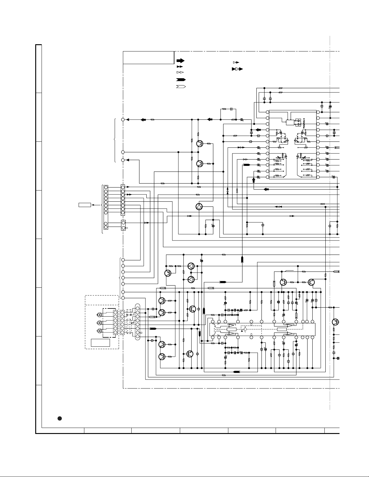
CHAPTER 6. CIRCUIT SCHEMATICS AND PARTS LAYOUT
[1] NOTES ON SCHEMATIC DIAGRAM
XL-G5000V/XL-G5000V(S)
•Resistor:
To differentiate the units of resistors, such symbol as K and M are
used: the symbol K means 1000 ohm and the symbol M means
1000 kohm and the resistor without any symbol is ohm-type resistor. Besides, the one with “Fusible” is a fuse type.
• Capacitor:
To indicate the unit of capacitor, a symbol P is used: this symbol P
means pico-farad and the unit of the capacitor without such a symbol is microfarad. As to electrolytic capacitor, the expression
“capacitance/withstand voltage” is used.
(CH), (TH), (RH), (UJ): Temperature compensation
(ML): Mylar type
(P.P.): Polypropylene type
• Schematic diagram and Wiring Side of P.W.Board for this model
are subject to change for improvement without prior notice.
REF. NO DESCRIPTION POSITION
SW1 CLAMP ON—OFF
SW1A PICKUP IN ON—OFF
SW2 TRAY SW1 ON—OFF
SW3 TRAY SW2 ON—OFF
SW4 DISC ON—OFF
SW601 SPAN SELECTOR 50/9
SW701 ON/STAND-BY ON—OFF
SW702 CLOCK/TIMER ON—OFF
SW703 REVERSE MODE ON—OFF
SW704 REVERSE PLAY ON—OFF
SW705 PRESET DOWN ON—OFF
SW706 P.B.C ON—OFF
SW707 O.S.D ON—OFF
SW708 DIGEST ON—OFF
SW709 CD ON—OFF
SW710 TUNER (BAND) ON—OFF
SW711 VIDEO/AUX ON—OFF
• The indicated voltage in each section is th e one measured by Digital Multimeter between such a section and the chassis with no signal given.
1. In the tuner section,
indicates AM
indicates FM stereo
2. In the main section, a tape is being played back.
3. In the deck section, a tape is being played back.
4. In the power section, a tape is being played back.
5. In the CD section, the CD is stopped.
• Parts marked with “ ” ( ) are important for
maintaining the safety of the set. Be sure to replace these parts
with specified ones for maintaining the safety and performance of
the set.
REF. NO DESCRIPTION POSITION
SW712 TAPE ON—OFF
SW713 REC/PAUSE ON—OFF
SW714 TUNING/TIME UP ON—OFF
SW715 TUNING/TIME DOWN ON—OFF
SW716 STOP ON—OFF
SW717 PLAY ON—OFF
SW718 PRESET UP ON—OFF
SW719 X-BASS/DEMO ON—OFF
SW720 EQUALISER ON—OFF
SW721 MEMORY/SET ON—OFF
SW722 DIRECT PLAY ON—OFF
SW723 DISC 1 ON—OFF
SW724 DISC 2 ON—OFF
SW725 DISC 3 ON—OFF
SW726 DISC 4 ON—OFF
SW727 DISC 5 ON—OFF
SW728 OPEN/CLOSE ON—OFF
SW801 VOLTAGE SELECTOR 230-240V
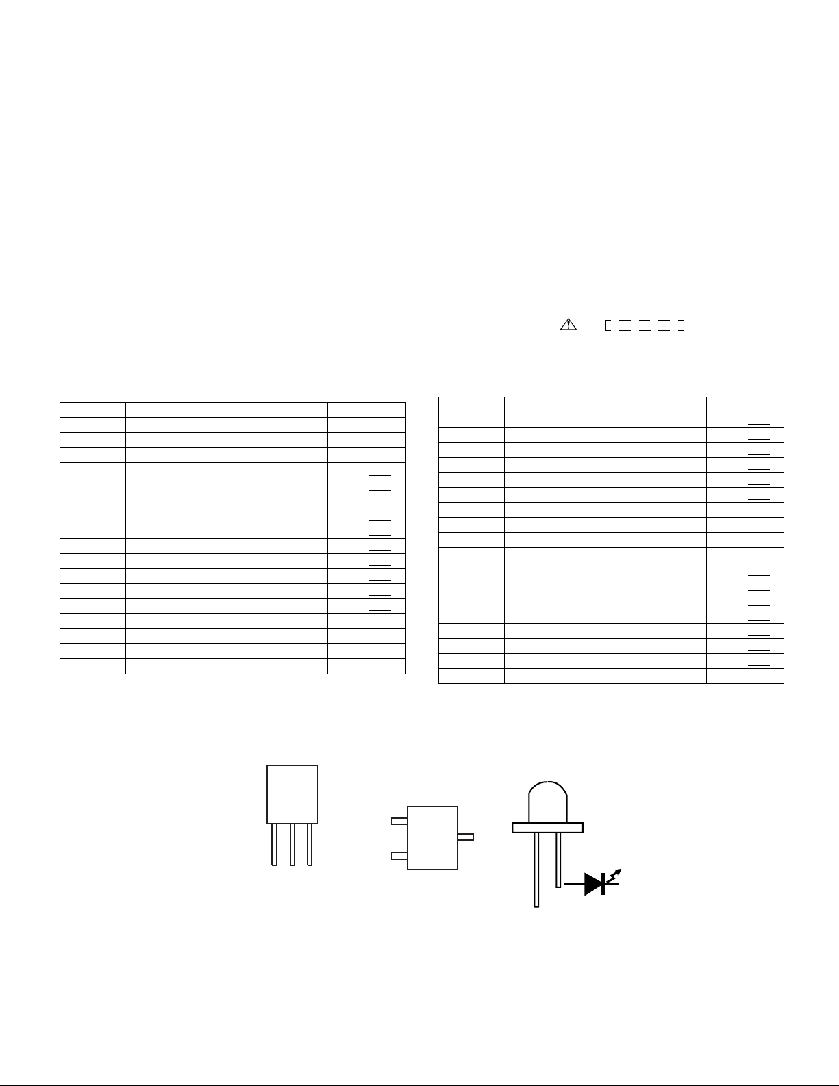
[2] TYPES OF TRANSISTOR AND LED
FRONT
VIEW
EC B
(S) (G) (D)
(1) (2) (3)
KTC3203 Y
KTA1271 Y
KTA1273 Y
KTA1274 Y
KTC3194 Y
KTC3200 GR
KTA1046 Y
B
(3)
E
TOP
VIEW
(1)
KTC3265 Y
KTA1504 GR
KTC3875 GR
KRC104 S
UN2211
KRC102 S
6 – 1
C
(2)
KRA102 S
KRA107 S
FRONT
VIEW
SVC347S
SVC230C
Page 25
XL-G5000V/XL-G5000V(S)
22K
0
(
Q
K
3
0
0039
0
[3] WIRING SIDE OF PWB/SCHEMATIC DIAGRAM
MAIN PWB-A1 (1/2)
A
FM SIGNAL
CD SIGNAL
AUX SIGNAL
VIDEO SIGNAL
MIC SIGNAL
PLAYBACK SIGNAL
RECORD SIGNAL
C641
0.0015
R623
1K
C609
C605
B
6-4 1 - D
TO MAIN PWB(2/2)
C
CNP601
CNS9
R-CH
1
CD_A_GND
2
L-CH
3
CD_GND
4
6-13 11 - D
CNP6
TO VCD PWB (1/2)
D
5
6
7
8
9
10
A_+8V
CD_D_GND
LD+8V
D_5V
V_DAC
D_GND
L_CH
1
A_GND
2
R_CH
3
1
2
3
4
5
6
7
8
VIDEO OUT
2
GND
NC
1
BIV1
R619
330
390
R613
R611
27K
2.2K
R615
Q601
KTC3875GR
27K
R610
R614
2.2K
Q602
KTC3875GR
390
R646
R612
R645
10K
10K
Q607
KRA107S
22K
R621
C639
2.2/50
R618
330
1/50
8.2K
C607
0.15
R607
(ML)
3.9K
C605
C611
1800P
C613 1/50
C615 4.7/50
C617
C619
C621
C623
1/50
2.2K
R609
R601
R6021K1K
220P
220P
C652
C651
IC601
LC75341
D1
1
CE
2
3
VSS
LOUT
4
LBASS
5
0.12
LTRE
(ML)
6
LIN
7
LSELO
8
L4
1/50
9
1/50
L3
10
1/50
L2
11
L1
12
C625
1000P
CCB
INTERFACE
TUNER
AUX
DECK
CD
VREF
ROUT
RBASS
RTRE
RSELO
220P
C653
C601
C602
220/16
CLK
24
23
VDD
C603
22
22/16
21
20
19
RIN
18
17
R4
16
R3
15
R2
14
R1
13
C614
C616
C618
C620
C622
C606
0.12 (ML)
C624 1/50
C626
1/50
4.7/50
1/50
1/50
1/50
1000P
C6
0.15
R608
R149
CD_D_GND
23
6-4 1 - E~H
TO MAIN PWB(2/2)
6
5
4
3
2
1
CD_GND
26
CD_A_GND
24
APRO GND
0
D_GND (RDS)
4
TAPEA GND
0
N_GND
0
CNS102
6
5
4
3
2
1
BI102
C104
180P
8
7
6
5
4
3
NC
2
1
C103
180P
E
TAPE MECHANISM
Ass'y(211)
F
ERASE HEAD
R-CH
L-CH
RECORD/
PLAYBACK HEAD
HEAD PLATE
BLOCK(211-1)
G
0V
0V
0V
0V
0V
0V
0V
9.3V
9.3V
Q112
KTA1504GR-1+
Q102
KTC3200GR
R104
2.2K
0.7V
0.7V
R106
3.3K
Q104
KTC3200GR
Q103
KTC3200GR
0.7V
R105
3.3K
0.7V
R103
2.2K
Q101
KTC3200GR
R146
10K
8.6V
R147
10K
R148
4.7K
R109
0V
Q113
KRC104S
0V
0V
0V
Q114
KRC104S
R112 15K
47K
R108
0V
0V
4.7K
R110
4.7K
Q105
KTC3199GR
0V
0V
47K
R107
3.4V
3.4V
0V
Q106
KTC3199GR
C105
C106 1500P
1500P
H
150(1/4W)
C141
100/16
Q108
KTC3875GR
0V
56
R116
C112
C116
C114
100/16
560P
0.033
C110
R114
330P
1K
24 23 22 21
1
R113
1K
R120
R118
3.9K
100K
112K
Hich=T1
112K
23 4205196187178169151014111312
R119
C109
3.9K
330P
R117
C113
100K
0.033
C115
560P
C111
100/16
56
R115
R111 15K
47/25
C118
47/25
C117
R124
6.8K
R123
6.8K
2.2K
R122
NC
IC101
AN7345K
NC
2.2K
R121
C121
0.022
R150
15K
68K
R126
C124 270P
5.6K
R128
C126
Hich=Chrome
5.6K
R129
C143
3.3/50
15K
R127
270P
C123
22/16
1.5K
R130
R131 1.15K
REC_R
0.7V
R132
C128
C125
R133
C127
R138
22/16
R136
220K
Q107
220K
220/10
C134
R137
0V
0.022
R158
220
(1/4W)
C135
11.6 V
R142
1
0V
82
1/2W
47K
R143
22K
R144
C1
C137
0.047
820
C139
CC
V
KTC3875GR
R139
10K
10K
0.7V
10K
22/16
R134
100
C132
47/25
C133
C130 3300P
0.022
56K
RIPPLE
Nor/CrO2
56K
C131
47/25
10K
R135
100
C129 3300P
0.022
NOTES ON SCHEMATIC DIAGRAM can be found on page 6-1.
1
23
45
6
Figure 6-2 SCHEMATIC DIAGRAM (1/14)
6 – 2
Page 26
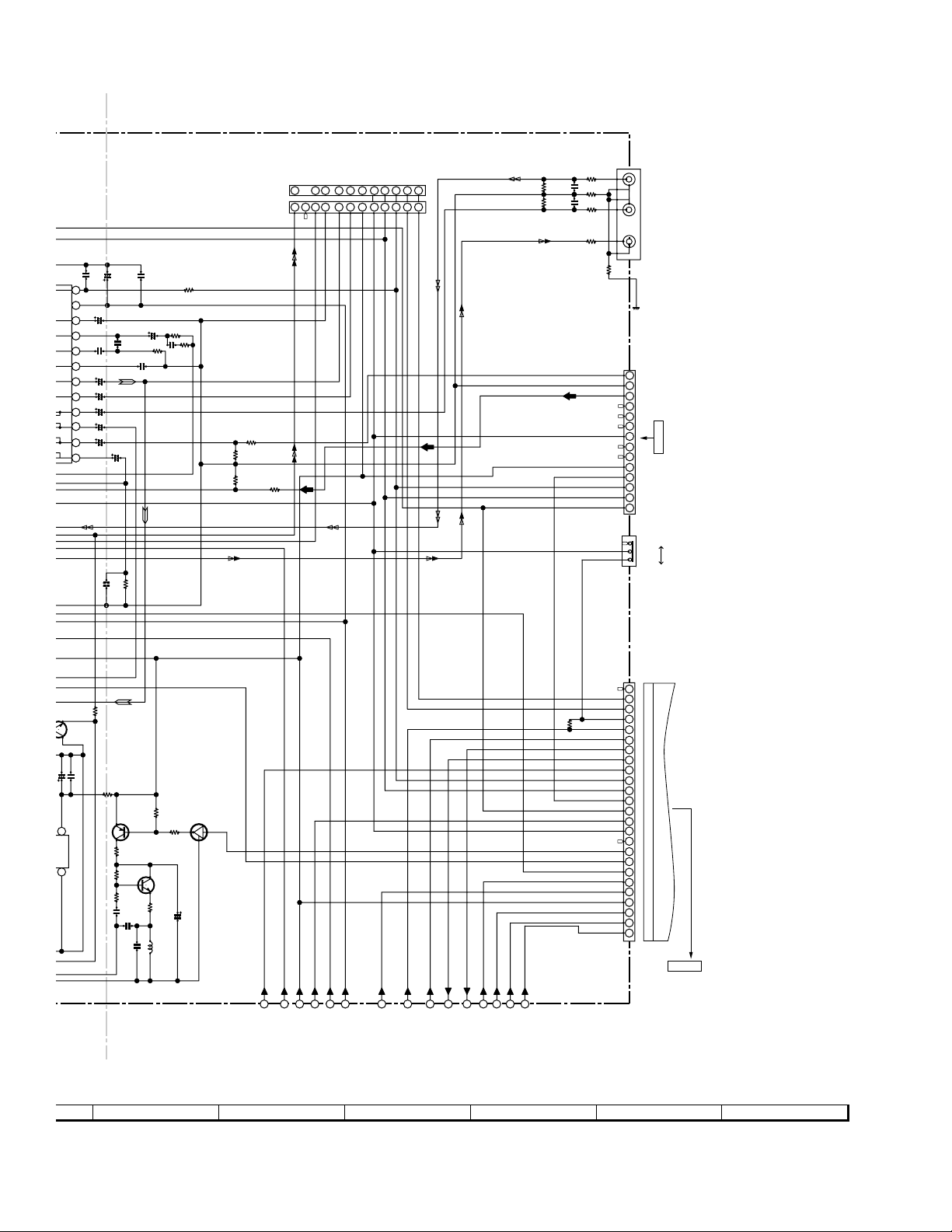
XL-G5000V/XL-G5000V(S)
C134
220/10
R693
15K
4
CNP303
SW601
SPAN
Lch
3
AUX IN
2
1
Rch
5
VIDEO OUT
JK690
6
JO311AW
R688
1ohm
CHASSIS
14
13
12
NC
11
NC
10
NC
9
8
NC
7
CNS303
6
5
4
3
2
1
NC
6-7 10 - H
FROM TUNER PWB
9KHz/50KHz
10KHz/100KHz
NC
A_GND
MIC OUT (L)
MIC OUT (R)
MICIN(L)
1 2 3 4 5 6 7 8 9 10 11
1 3 4 5 6 7 8 9 10 11 122
BIK1
NC
220P
C653
CLK
24
23
VDD
REF
22
OUT
21
ASS
20
TRE
19
C614
RIN
18
C616
ELO
17
C618
R4
16
C620
R3
15
C622
R2
14
R1
13
C601
C603
22/16
C606
0.12 (ML)
C624 1/50
220/16
1/50
4.7/50
1/50
1/50
1/50
C626
0.15 (ML)
1000P
R608
C602
C608
2.2K
0.022
C612
1800P
C610
R603
1K
R604
1/50
8.2K
R624
R606
1K
C642
3.9K
0.0015
R642
10K
2.2K
R644
R641
2.2K
R643
10K
DI
D_GND
A_+10V
MICIN(R)
KOK LATCH
CLK
MIC IN
CNS602
R691
R690
R09
0
C691
390P
1.2K
C690
390P
1.2K
R692
15K
R694
10
5000:CM010P
SELECTOR
Q107
TC3875GR
0V
13
CC
V
12
0.022
C135
R158
220
(1/4W)
11.6 V
R142
R137
25
NC
25
24
220K
0V
82
R143
C137
1/2W
47K
0.047
8200P
11.6 V
Q109
KTA1504GR-1+
0V
22K
R144
C138
C139
0.039
10K
R622
Q110
47K
R140
KRC104S
R141
4.7K
0V
0V
Q111
0V
KTC3203Y
4.7
R145
C140
47/25
L103
330µH
23
22
21
20
19
18
17
16
15
14
13
12
11
NC
10
9
8
7
6
5
4
3
2
1
1
FFC701
CNP701A
TO DISPLAY PWB
6-11 11 - B
131406418161712009805
-VF
VF1
SP_DET
LD_+8V
A_+10V
D_+5V
+B_PROTECT
A_+8V
SW_+5V
UNSW5.6V
P_IN
SP_RLY
AC_RLAY
M_+13V
VF2
TO POWER SECTION
7 8 9 10 11 12
Figure 6-3 SCHEMATIC DIAGRAM (2/14)
6 – 3
Page 27
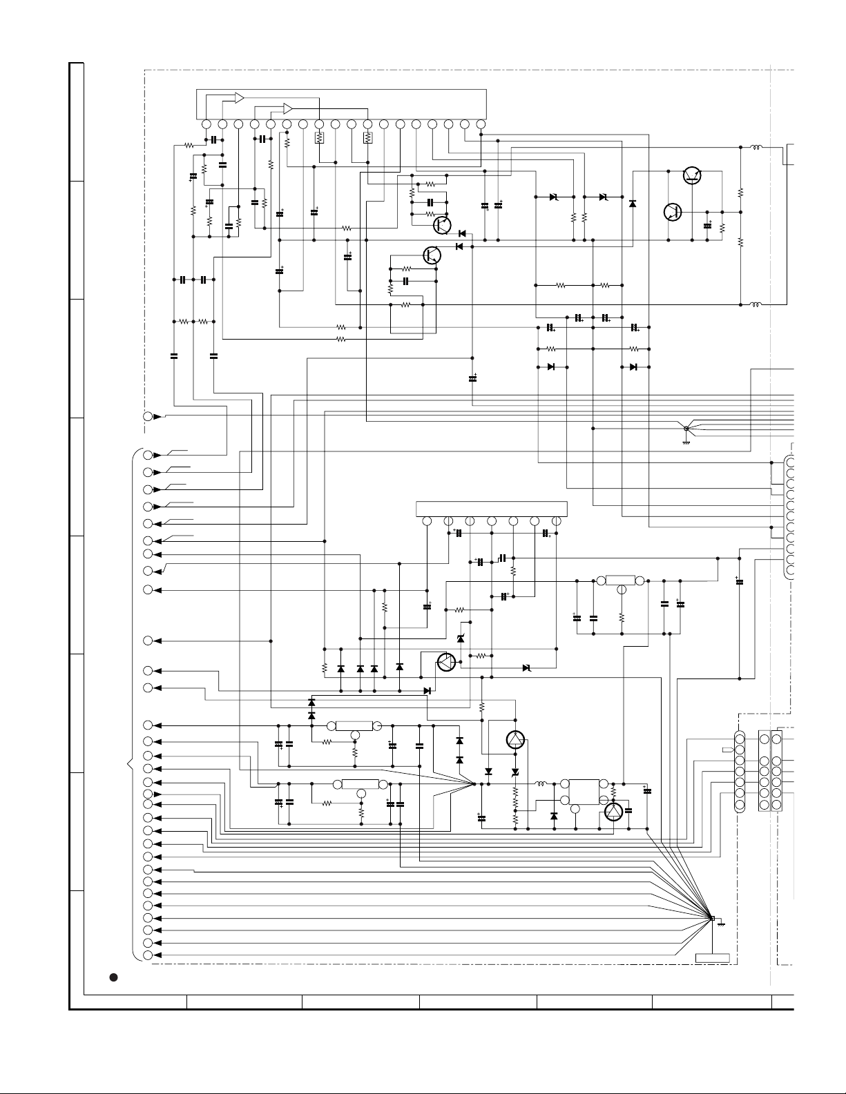
XL-G5000V/XL-G5000V(S)
0
10(1/2W)
+
-
18 17 16 15 14 1213 1011 9 8 7 6 5 4 3 2 1
C905
10/50
C907
100P
R903
1K
C908
3.0P
R907
56K
C906
10/50
R905
560
R906
560
C910
C909
0.1(ML)
A
B
C904
C903
560P
560P
R901
R902
56K
56K
C902
C901
0.047
C
D
0.047
AC_RELAY
0
L_CH
1
A_GND
2
R_CH
3
SP_RLY
4
SP_DET
5
M_+13V
6
LD_8V
0
A_+8.5V
18
A_+10V
8
E
SW_+5V
10
+B_PROTECT
9
DVD_PROTECT
19
F
TO MAIN SECTION
G
H
DVD_1.5V
20
DVD_A3.3V
21
DVD_D3.3V
22
DVD_A5V
11
DVD_S5V
12
DVD_FUNC
23
VF2
13
VF1
14
-VF
15
P_IN
16
UNSW5.6V
17
A_GND
24
M_GND
25
TAPE A GND
26
D_GND(RDS)
27
DVD_AGND
28
DVD_DGND
29
DVD_MGND
30
DVD_A_GND
0
-
VL-
VH-
100/100
D861
1N4148H
LD1117V
1
IC855
LD1117V33
VOLTAGE
REGULATOR
1
27
R876
GND
R916
0.22(3W )
R917
0.1(3W)
R918
1.5K
C917
0.01(ML)
R919
1.8K
D906
1N4148H
Q902
KTC3875GR
Q901
KTC3875GR
R920
1.8K
R921
C919
1.5K
0.01(ML)
R922
0.1(3W)
22K
R864
D860
1N4148H
D993
C880
C879
10/50
47
R882
C875
10/50
D876
C864
22/25
1N4148H
0.1
0.1
10V
D868
1N4148H
D905
1N4148H
SP_DET
8.5V
7 1 4 3 5 26
C859
22/25
R857
ZD860
Q860
KRC104S
D882
C946
0.1/50
22K
DZ110BSB
RL204F
+
C913
R912
100P
100(1/4W)
R913
D994
MA111
D995
MA111
C881
C877
0.1
0.1
0.22(3W )
C914
100/100
R958
100(1/4W)
R908
22K
R863
D862
1N4148H
2 3
R881
120
2 3
R875
330
R910
1K
C915
1K
IC856(1.5V)
VOLTAGE
REGULATOR
R904
1K
3.0P
R909
33K
56K
R911
C911
100/100
C912
100/100
C882
47/25
C878
47/25
POWER AMP
STK41240-1
VH+
VL+
C916
100/50
IC851
AN80T53
MULTI REGULATOR
5.1V
C865
22/25
R859
10K
R972
320
D883
RL204F
D865
1N4148H
C872
470/10(UHD)
C874
C855
10/50
IC901
100/50
GND
0.1
R866
2.2K
R867
1.8K
R865
1K
C918
ZD804
DZ6R8BSB
VCC
R854
3.3K
ZD805
DZ150BSB
Q853
KRC102S
R
R937
56K
NC
UNSW_5.6V
0001AW
1
2
3
4
5
6
7
BI802
L902
Z0024
R934
56K
R935
56K
L
L901
Z0024
R939
1
2
3
4
5
6
7
8
9
10
11
C856
6800/35
BI801
1 1
2 2
3
3
4
4
5
5
6
6
CNS802
CNP802
Q903
KTC3875GR
ZD902
DZ120BSB
1.5K(1/2W)
39(1/4W)
C920
3300/71
R929
47(1/4W)
D909
1N4004S
VH-
SW
C854
220/25
MODE 1
L801
100µH
ZD903
DZ120BSB
D907
47K(1/4W)
VL+VL-
IC852
7808
VOLTAGE
REGULATOR
2
R874
10K
C923
3300/71
R930
D910
1N4004S
R850
0
1N4148H
Q904
KTC3875GR
C925
47/50
VH+
CHASIS
C851
C866
0.1
47/25
C868
220/35(UHD)
R884
0.1
-VF
VF1
VF2
P_IN
C925
C926
1.5K(1/2W)
R927
13V
C867
22/25
R928
39(1/4W)
C922
C921
4700/35
4700/35
3 1
C852
0.1
1
2
IC853
SD9701T
5
4
3
Q866
KRC107S
D866
D1FH3
HEATSINK
NOTES ON SCHEMATIC DIAGRAM can be found on page 6-1
1
23456
Figure 6-4 SCHEMATIC DIAGRAM (3/14)
6 – 4
Page 28
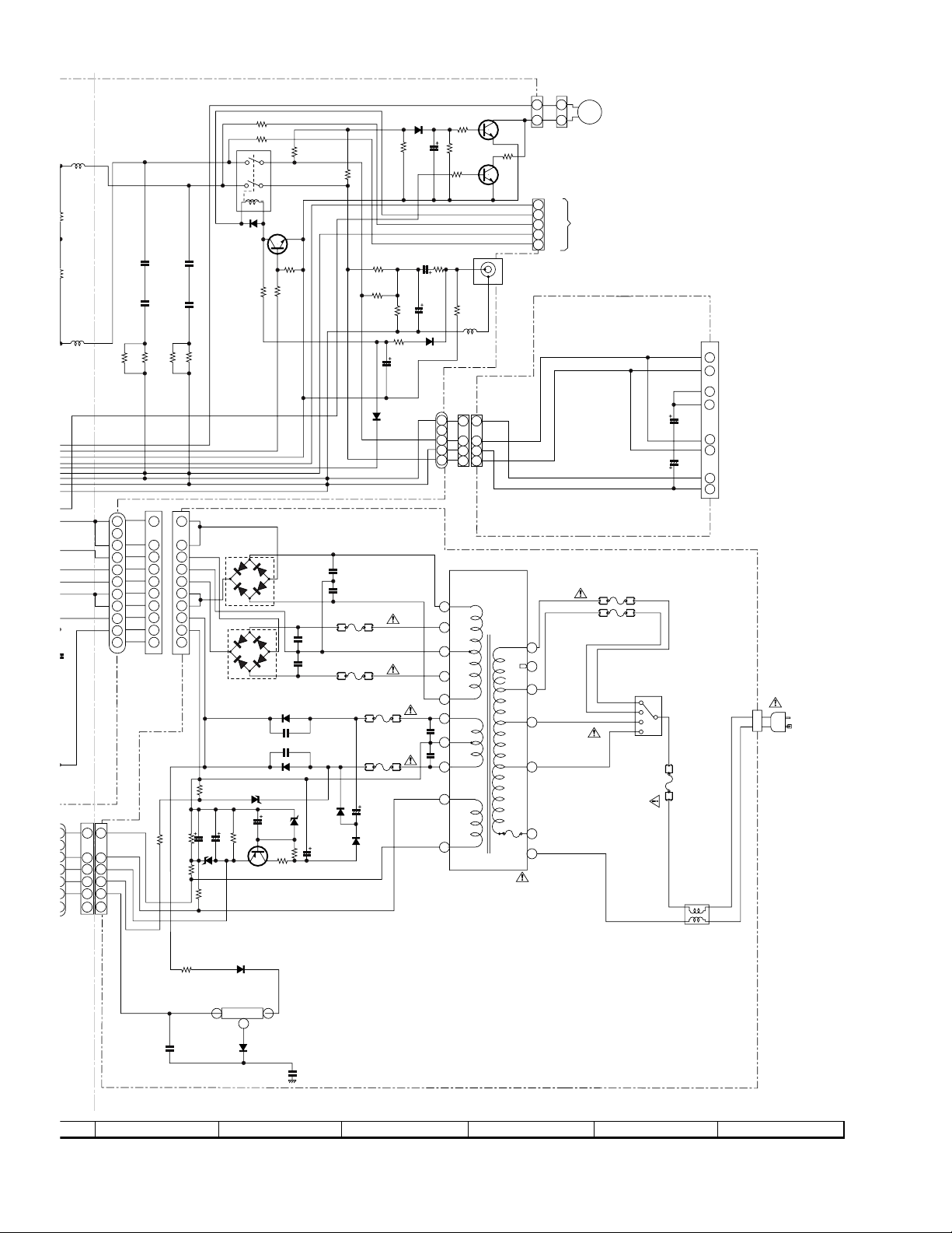
XL-G5000V/XL-G5000V(S)
BI802
2
+
R_CH
GND
L_CH
2
FAN MOTOR
M
121
1
2
3
4
5
CNS971CNP971
WTM901
W019EAW
-
TO H/P/PWB
FW901
2746AW
FRONT : 8 OHMS
REAR : 16 OHMS
1
REAR_SP_LCH
REAR_SP_RCH
REAR_SP_LCH_GND
F805
T4A L 250V
FH809 FH810
L841
LINE FILTER
REAR_SP_RCH_GND
LCH
RCH
LCH_GND
RCH_GND
CNP805
LIFE
NEUTRAL
AC SUPPLY
50/60Hz
110/127/220/230-240V
C947
22/50
C948
22/50
S0901
A0813AW
T2A L 250V
F807
FH814
FH812 FH811
1
NC
2
3
4
5
6
7
F806
T2A L 250V
230-240V
220V
127V
110V
FH813
SW801
VOLTAGE
SELECTOR
R942
390(2W)
R
R943
390(2W)
L
R
L902
Z0024
R
R934
56K
R935
56K
L901
Z0024
C856
6800/35
1 1
2 2
3
4
5
6
CNS802
L
D911
1N4148H
R926
C927
0.22(ML)
0.22(ML)
R973
10(1/2W)
R802
47K
C801 100/35
ZD801
R805
47(1/4)
C802 47/50
D3SBA60F
R806 47K
Q801
KTA1274Y
22K
D802
ZD802
DZ6R8BSB
R929
R928
0.22(ML)
0.22(ML)
L
R939
R941
10(1/2W)
10(1/2W)
1
2
3
4
5
6
7
8
9
10
11
BI801
3
4
5
6
CNP802
1
2
3
4
5
6
7
8
9
10
R801
CNS801
100K
R938
10(1/2W)
R803
12K
R804
47(1/4)
R940
VH-
1
2
VL-
3
GND
4
VL+
5
VH+
6
7
8
9
10
CNP801
DZ6R2BSA
Q905
KTC3875GR
D803
RL204F
C803
47/50
10(1/4)
RL914
RELAY
R946
47K
R956
0
D10XBA60F
D804
RL204F
R808
R807
0.2
4.4
D801
C806
0.1(ML)
C807
0.1(ML)
2.2K(1/2W)
R945
1.5K
C809
0.1(ML)
C808
0.1(ML)
ZD803
DZ300BSB
R944
2.2K
T4A L 250V
FH803
T4A L 250V
FH801
D805
1N4004S
C804
220/63
C810
0.22/100
C811
0.22/100
F802
F801
R1_OUT
FH804
FH802
T2A L 250V
FH807
T2A L 250V
FH805
C805
D806
L1_OUT
R966
6.8K(1/2)
R965
6.8K(1/2)
22/100
1N4004S
D912
1N4148H
C931
R947
10/50
15K
R974
0
C961
10/50
C960
3.3/25
R968
560(1/2)
R969
D913
22K
1N4148H
C963
220/16
D996
1N4148H
L
R
F804
FH808
F803
FH806
Q906
KTC3203Y
R949
1K
R950
68K
R960
1K
Q907
KTC3203Y
R967
100K
L903
2.2µH
CNP902
CNS902
BI902
1
1
1
2
3
2
2
4
3
3
5
4
4
11
12
13
14
15
8
0.22
C815
9
0.22
C816
10
16
17
PT801
POWER TRANSFORMER
(MAIN)
R951
100
M_+13.5V
SP_RLY
JK953
SUBWOOFER
PRE-OUT
TF801
150°C
R844
82(1/4W)
C861
0.022
7
D853
1N4004
IC854
78L05
VOLTAGE
3 1
REGULATOR
2
D856
1N4148H
C890
0.047
8 9 10 11 12
Figure 6-5 SCHEMATIC DIAGRAM (4/14)
6 – 5
Page 29
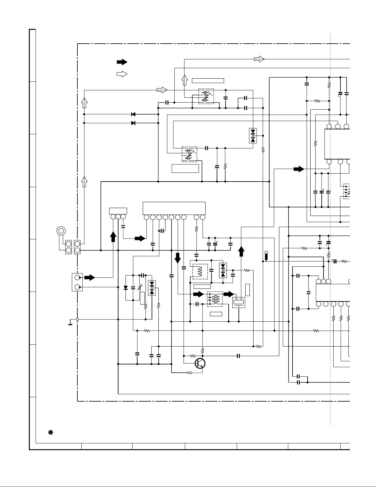
XL-G5000V/XL-G5000V(S)
1
3
AIN
REG
/
0
0
3
C392
A
FM SIGNAL
AM SIGNAL
AM TRACKING fL
T303
2
3
AM OSC.
T306
6
4
5
3
7
C310
R302
15P(CH)
C312
0.022
R325
47K
R327
33
4
5
6
AM ANT.
C335
560P
2
1
9
8
10
C306
C311
T301
FM OSC
+B
C334
22P
(CH)
+B
0.022
18P
(CH)
R322
680
Q302
KTC3194 Y
C323
D302
DS1SS133
C304
0.01
C309
0.001
L312
FM RF
R311
100K
R314
22
0.01
0.022
C316
0.022
AM BAND
COVERAGE fL
FM FRONTEND
IC301
TA7358AP
5
4321
6
C305
4.7P
(CH)
VD302
SVC230C
0.001
C320
33K
R313
C317
0.001
D301
B
DS1SS133
C
BAND PASS
FILTER
BF301
D
E
AM
LOOP
ANTANNA
1
SO302
FM ANTANNA
CNP301
212
TERMIANL
321
C303
100P(CH)
C308
DS1SS133
D305
(CH)
4.7P
F
CHASSIS
GND
C315
G
1
VD303
SVC230C
(CH)
4.7P
C324
T302
FM IF
C307
10/16
C330
15P
(CH)
SVC347S
R323
68K
22P
C313
1
VD301
C343
0.022
(CH)
2
3
C318
100P
10K
R309
FM IF
CF303
C331
0.047
C332
0.022
R336
10.7MHZ
R316
4.7K
10K
+B
TP301
12P
+B
+B
C342
0.022
R358
3.3K
+B
5.6K
R351
0.022
10/16
C351
C352
+B
C397
0.022
R382
150
C381
C382
15P
(CH)
(CH)
X352
IC302
LC72131
22 21 20
XIN
4.5MHZ
PLL(TUNER)
R375
470
C384
0.001
C302
0.001
FM IF IN
12
0.022
C350
C393
VSS
XOUT
AOUT
251
10K
R365
C362
2.2/50
AM OSC IN
AM OSC OUT
C394
47/16
10K
R381
1/50
CE
34
1K
1K
R374
222324
AM MIX OUT
R380
1.5K
DI
R373
C361
T
C
10
1K
R372
22
.
FM AFC
CL
H
NOTES ON SCHEMATIC DIAGRAM can be found on page 6-1
1
23456
Figure 6-6 SCHEMATIC DIAGRAM (5/14)
6 – 6
Page 30
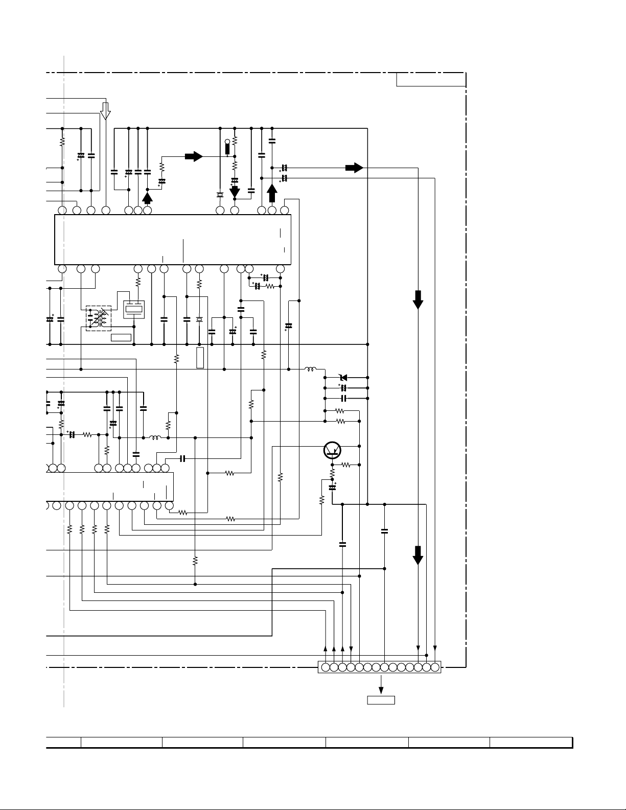
XOUT
10/16
C352
R365
8
C362
AM OSC OUT
FM IF IN
123
0.022
C350
C394
47/16
10K
R381
C393
1/50
21 20
VSS
AOUT
CE
34
2
1K
2
131
R)
R374
10K
2.2/50
AM OSC IN
AM MIX OUT
R380
1.5K
DI
1K
R373
C361
FM AFC
T351
C380
10/50
CL
5
1K
R372
0.022
REG
C392
0.001
AIN
AM RF IN
PD
DO
6
1K
R378
0.022
C363
AM IF
2.2K
R379
FM/AM
7
2.2/50
C364
1
2
C387
VDD
VSM
0.022
FM IN
IF
8
0.001
0.022
C366
C365
AM LOW CUT
FM/AM OUT
AM IF IN
GNDSDSTEREO
4
6
5
1K
R352
3
CF352
C353
C389
0.001
L351
100µH
0.01
C385
1213141516171819
SD
AM IN
MO/ST
CONT
FM/AM
91011
R357
R356
FM DET
270
10.7MHZ
FM IF
22K
X351
456KHZ
C399
MPX VCO
VCC
0.022
+B
R395
47K
TP302
MPX IN
C398
100/10
R360
4.7K
C368
IF OUT
C356
0.001
2.7K
R350
1/50
C367
78 9 1011 12
R353
0.022
C354
0.022
CF351
1K
R393
47K
R377
+B
C386
330P
IF IN
ST IND
R376
1K
R386
470K
1K
1/50
PHASE
C357
2.2/50
C355
C374
0.015
(CH)
C369
27P
R-CH OUT
22P(CH)
R388
5.6K
R387
C373
C371
1/50
C372
1/50
131415161718192021222324
L-CH OUT
3.9K
0.015
MO/ST
(FM/AM)
PHASE
C358
1/50
R355
3.3K
1/50
C370
R359
1.8K
IC303
LA1832S
FM IF DET./FM MPX./AM IF
L352
100µH
C396
100/10
C395
0.022
270
270
Q360
KTA1504 GR
5.6K
R385
5.6K
R384
C383
100P
ZD351
DZ5.1BSB
R392
(1/4W)
R391
(1/4W)
R383
5.6K
C391
47/16
+B
+B
TUNER PWB-C
C388
0.001
XL-G5000V/XL-G5000V(S)
D_GND
A_+10V
DI
CLK
DO
CE
CNS303
7
8 9 10 11 12
1234567891011121314
CNP303
6-3 12 - C
TO MAIN PWB(1/2)
A_GND
TUN_L
TUN_R
Figure 6-7 SCHEMATIC DIAGRAM (6/14)
6 – 7
Page 31

XL-G5000V/XL-G5000V(S)
10K
10K
A
MIC PWB-G
B
LUGK1
CHASIS
GND
C
JK1
MIC 1
D
JK2
MIC 2
E
VRK1
MIC
F
LEVEL
DK1
1SS133
DK2
1SS133
CK3
220P
3
2
1
4
5
7
8
3
2
1
4
5
7
8
3
2
1
2
3
0.1
CK75
CK54
MIC SIGNAL
CK41
100/16
+B
ICK1
MICSW
1
MCLKCONT
2
VALC
3
MIC1IN
4
ALC1
5
MIC1NFIN
6
MIC1OUT
7
MIC1VOLIN
8
MIC2IN
9
ALC2
10
MIC2NFIN
11
MIC2OUT
12
MIC2VOLIN
13
MICOUT
14
LPF1IN1
15
LPF2IN2
16
17
LPF1OUT
ADINTOUT
18
19
ADINTIN
20
ADCONT
21
REF
M65856SP
MIC AMP.
SOURCEOUT
KEYCONIN
LPF2OUT
LPF2IN2
LPF2IN1
DAINTOUT
DAINTIN
DACONT
DATA
CLOCK
LATCH
PS2
PS1
VCFIL
LOUT
ROUT
RIN
LIN
VOLIN
VCC
GND
CK35
47P
CK34
CK33
0.15
2.2/50
2.2/50
2.2/50
2.2/50
2.2/50
4.7K
0.001
0.0047
0.068
0.22
(CH)
47P
(CH)
47P
(CH)
CK19
0.022
42
41
40
39
38
37
36
35
34
33
32
31
30
29
28
27
26
25
24
23
22
RK10
RK9
CK31
CK29
CK30
CK26
CK25
CK24
RK73
CK23
CK22
CK21
CK20
100/16
1K
1K
CK18
1K
RK11
RK3
56K
0.01
CK1
10K
RK4
5.6K
RK71
0.1
RK8
RK70
5.6K
RK7
1K
CK13
0.0047
CK70
1K
CK71
CK72
CK73
CK74
CK7
CK8
CK9
CK10
CK11
CK12
CK14
RK72
CK15
CK16
CK17
56K
0.47/50
4.7/50
2.2/50
0.1
0.1
0.47/50
4.7/50
2.2/50
0.1
0.1
2.2/50
0.001
4.7K
0.068
0.22
220/10
10K
(ML)
(ML)
RK1
RK2
+B
+B
CK42
0.022
RK50
RK49
G
H
NOTES ON SCHEMATIC DIAGRAM can be found on page 6-1
1
23456
Figure 6-8 SCHEMATIC DIAGRAM (7/14)
6 – 8
Page 32

XL-G5000V/XL-G5000V(S)
+B
CK48
220P
8.2K
10K
10K
RK48
QK1
KTC3203 Y
CK43
47/16
RK47
10K
CK53
47/16
RK12
100
+B
RK13
1.2K
ZDK1
DZ5.6B
+B
RK50
RK49
+B
CK42
0.022
RK45
6.8K
CK51
47/16
CK52
47/16
RK44
6.8K
RK46
18K
CK50
CK49
RK43
18K
CK47
220P
100P
(CH)
100P
CK44
47/16
2
3
(CH)
5
6
100
100
ICK2
TJM4558CD
OPE AMP.
8
–
1
+
+
7
–
4
RK14
(1/2W)
RK15
(1/2W)
CK46
2.2/50
CK45
2.2/50
RK42
10K
RK38
100
CK40
100/16
10K
RK41
RK37
390
RK39
1K
RK36
390
RK40
CNPK1
MICOUT(L)
MICIN(L)
A_GND
MICOUT(R)
MICIN(R)
A_+10V
1K
KARA LATCH
MIC IN
+B
CLK
1
2
3
4
5
6
CNSK1
7
DI
8
9
10
11
6-3 11 - F
FROM MAIN PWB(1/2)
7
8 9 10 11 12
Figure 6-9 SCHEMATIC DIAGRAM (8/14)
6 – 9
Page 33

XL-G5000V/XL-G5000V(S)
G
T
Y
B
A
K
S
2
T
D
N
N
S
O
K
O
P
Q
E
T
T
N
D
T
K
F
R784
DISPLAY PWB-B1
A
+B
R756
150
R574
150
LED707
SDPB50CD
Q710
KRC102 S
3
B
LED PWB-B3
LED708
A304BC2H
R573
150
BI707
Q711
S
KRA102
1
2
1
2
R772
150
CNP707
3
1
1
2
2
CNS707
2
1
C
10K
10K
10K
10K
R760
R759
R758
R757
CNP705
1
MOT A+
1
MOT A-
2
MOT B+
3
MOT B-
4
POWER
MPEG
5
DSA_ACK
6
DSA_DATA
CNP7
6-15 12 - C
D
E
F
TO VCD PWB(2/2)
SWITCH PWB-B2
SW728
OPEN/
CLOSE
10K
RD25
SW727
DISC 5
5.6K
RD24RD22
SW726
DISC 4
3.9K
RD23
SW725
DISC 3
2.7K
SW724
DISC 2
2.2K
RD21RD20
SW723
DISC 1
1.5K
SW722
DIRECT
PLAY
RD19
1K
BI703B
7
DSA_STB
8
ESS_DO
9
ESS_DI
10
ESS_STB
11
ESS_ACK
12
12
FFC7
2
1
BI703A
2
1
TAPE MECHANISM Ass'y(211)
SOLENOID
10K
R777
R778
GND
KEY
1.5
R766
1/50
C707
1K
R745
10K
10K
R765
10K
R561
P20
P19
P16
P17
P18
F2
F2
NP
NP
454443424140393837363534333231 30292827262524232221201918171615141312111098765
47K
R763
D704
(SPC ONLY)
R563
4.7K
R562
4.7K
4.7K
R565
R749
R564
+B
4.7K
4.7K
P14
P15
C724
0.047
D712
MA111
Q714
KRC104 S
2
1
P13
P12
3
P10
P11
Q715
KRA107 S
2
1
G
R774
R773
4.7K
8.2K
R566
8.2K
M
TAPE
MOTOR
(211-2)
–
+
END SW
–COM
+SOL
+MTR
N.C. (OP PACK)
F. REC
R. REC
TAPE MECHANISM
PWB Ass'y(211-3)
1
1
2
3
4
5
6
7
77
FFC702
1
T1
1
GND
2
T_SOL_A
3
T_MOTOR
4
5
FPA
6
FPB
7
CNP702
RUN
P08
P09
R750
R741
R742
R743
R744
R748
R753
R737
R736
R761
R747
R740
R739
R738
3
FL701
NA-11SS55-1
FL DISPLAY
P07
NX
NX
81 82 83 84 85 86 959493929190898887
S9
80
S10
VLOAD
79
S11
78
S12
77
S13
76
S14
75
S15
74
S16
73
S17(DIST 3)
72
S18(DIST 2)
71
S19(DIST 1)
70
S20(DIST 0)
69
68
67
1K
MPEG_PWR
66
1K
65
MOT_A+
1K
64
MOT_A-
1K
MOT_B+
63
1K
MOT_B-
62
61
60
KARA_LATCH
1K
MIC_SW
59
1K
58
ILLU_LED
DIST
57
1K
56
CLAMP SW
1K
DISC SW
55
1K
TRAY SW1
54
1K
TRAY SW2
53
1K
RDS-RDCL
52
ESS-DI
1K
RDS-RDDA
51
ESS-STB
1K
R793
1K
LED701
304VT2H3
Q712
KRC104 S KRA107 S
3
2
1
Q701
KTA1273 Y
Q702
KTA1271 Y
D711
MA111
P05
P06NXNXNXNX
S8S7S6
S5
MICROCOMPUTER
RDS-READY/ESS DO
50 49
VDD
SP_RLY
AC_RLY
1K
1001K1K
R771
R735
R733
R746
5V BACK UP
+B
Q713
3
2
1
R732
+B
R775
10K
R776
10K
P03
P04
S4S3S2
RDS-RST/ESS ACK
T_MOTOR
VOL_LED
2.2K
P01
P02
S1
IC701
IXA034AW
SYSTEM
TIME LED
T_SOL
41 40 39 38 37 36 35 34 33 32 3150 49 48 47 46 45 44 43 42
560
R734
R782
+B
R731
G11
G10G8G7G6G5G4G3G2G1
G9
G9
G10
G11
CD_RESOU
TUN_SM/SPA
FPA/FPB SW
PHOTO
SMUTE
VSS
REMOCON
P_IN
AVREF
SP DET
1K
1K1K1K
R729
R728
CNP706B
4.7K
C716
0.001
1
R727
9
8
7
6
5
4
3
2
1
R780
2.7K
R726
3
+B
2
VR701
VOLUME
R725
1N4148 (1K)
D713
4.7K
680
R779
R781
4.7K
–20dBAT
T_BIA
T_REC/PLA
DSA_ST
CD_WR
DSA_DAT
DSA_AC
RESE
CD_DR
CD_CE
CD_CL
CD_D
CD_D
T_RU
PROTEC
VOL_JO
AVDD
KEY 0
KEY 1
1K
C717
0.001
XOU
AVS
R724
10099989796
G1
G2G3G4G5G6G7G8
VD
XI
VP
XT
VD
CL
D
D
C
KEY 2
1K
H
NOTES ON SCHEMATIC DIAGRAM can be found on page 6-1
1
23456
Figure 6-10 SCHEMATIC DIAGRAM (9/14)
6 – 10
Page 34

G7G6G5G4G3G2G1
1110987654321
9594
G7PHOTO
ER
P_IN
37 36 35 34 33 32 31
1K
1K
R727
R726
706B
9
8
7
6
5
4
3
2
1
99989796
–20dBATT
T_BIAS
T_REC/PLAY
DSA_STB
CD_RESOUT
CD_WRQ
DSA_DATA
DSA_ACK
RESET
CD_DRF
CD_CE
CD_CLK
CD_DI
CD_DO
T_RUN
TUN_SM/SPAN
FPA/FPB SW
PROTECT
VOL_JOG
AVREF
AVDD
KEY 0
1K
R725
XOUT
AVSS
KEY 1
R724
NPNPF1
100
G1
G2G3G4G5G6
1
VDD
D714
2
R701
3
R702
4
R703
5
R704
6
R705
7
R706
8
R707
9
R708
10
11
XIN
12
4.19403MHz
VPP
13
XT2
14
R709
15
VDD
16
R710
CLK
17
R711
DI
18
R712
DO
19
R713
CE
20
R714
21
R715
22
R716
23
R717
24
25
26
27
28
29
30
680
R755
KEY 2
1K
R723
1K
XL-G5000V/XL-G5000V(S)
CNP701A
MA111
25
24
23
22
21
20
19
18
17
16
15
14
13
12
11
10
9
8
7
6
5
4
3
2
1
CNP704
14
13
12
11
10
9
8
7
6
5
4
3
2
1
25
1
14
1
FFC701
TO VCD PWB(1/2)
FFC5
CNP701B
6-3 12 - F
TO MAIN PWB(1/2)
CNP5
6-13 11 - B
R04
0
R01
+B
0
F1
R795
1.5
C700
1/50
C701
1000/6.3
+B
MA111
1K
1K
100
1K
1K
1K
1K
1K
C703
15P
C702
(CH)
XL700
1K
1K
1K
1K
1K
1K
1K
1K
1K
R720
R719
1K
1K
C704
18P(CH)
FFC706
9
8
7
6
5
4
3
2
1
C705
0.022
R721
1K
R790
5.6K
CNP706A
R789
0.022
+B
10K
10K
R791
+B
+B
R783
Q719
KRC104 S
10K
+B
R770
10K
3
2
1
C723
0.047
R020
R025
+B
R788
10K
R722
10K
R792
10K
0
0
+B
+B
+B
+B
+B
UN_SW5.6V
RDS-RDCL/MIC_SWITCH
RDS-READY/KARA_LATCH
TUN_SM/SPAN
UNSW5.6
P_IN
SP_RLY
AC_RLY CON
SP_DET
+B_PROTECT
D_GND
S_MUTE
T_BIAS
REC/PLAY
–20dB
M_+13V
SW_5V
A_+10V
TRAY SW2
TRAY SW1
CD_CLK
CD_DRF
CD_WRQ
CD_RESOUT
D708
MA111
CLK
DI
DO
CE
–VF
VF1
VF2
GND
PHOTO
CLAMP
CD_CE
CD_D1
CD_D0
+5V
DISC
D709
C718
REC/
KRC102 S
2
0.01
D705
MA111
Q703
3
1
RD13RD12
SW714
TUNING
/TIME
UP UPDOWN
+B
D706
MA111
C719
3.3/50
D707
R797
MA111
3.9K2.7K2.2K 5.6K
TUNING
/TIME
RD06RD05
P.B.C O.S.D
RX701
GP1UM271
REMOTE
SENSOR
100K
C722
150P(CH)
RD15
SW716 SW717SW715
STOP PLAY
RD07
123
C720
RD16RD14
10K
SW708SW707
DIGEST
0.022
+B
PRESET
R798
100
SW718
C721
47/16
+B
+B
RD18
SW720
EQUALISER
SW710SW709
TUNER
(BAND)
RD02
SW702
CLOCK/
TIMER/
820
SW703
REVERSE
MODE
VIDEO
/AUX
RD03
100µH
L701
SW721
MEMORY
/SET
RD10RD09
47K
R796
1.5K1K
SW712SW711
TAPE
RD04
REVERSE
PLAY
SW713
PAUSE
SW705SW704 SW706
PRESET
DOWN
1K
10K
R718
R784
+B
KEY 2
M_+13V
R780
2.7K
2
1
3
VR701
VOLUME
C717
KEY 1
KEY 0
0.001
7
+B+B
R799
5.6K
+B
R785
10K
+B
R786
10K
R787
10K
R794
10K
RD17
680
SW719
X-BASS
/DEMO
RD08 RD11
680 820
CD
RD01
680 820 1K 1.5K 2.2K 2.7K 3.9K
SW701
ON/
STANDBY
8 9 10 11 12
Figure 6-11 SCHEMATIC DIAGRAM (10/14)
6 – 11
Page 35

XL-G5000V/XL-G5000V(S)
E
V
C
S
S
H
D
D
X
M
S
C
C
C
F
S
A
C
4
6
A
B
C
D
E
PICKUP UNIT(306)
VCC
E
A
B
F
C
TR+
FO+
FO–
TR–
GND
LD
VREF
PD
VR VR
TR+
FO–
FO+
TR–
VCD PWB-D(1/2)
C33
0.022
C32
100P(CH)
C34
VIDEO SIGNAL
CD SIGNAL
C1
47/25
+B
C2
0.01
C38
16
15
14
13
12
11
10
9
8
7
6
5
4
3
2
1
FFC1
LD
15
VREF
14
PD
13
VCC
12
11
R6
E
10
R5
A
9
R4
B
8
R3
F
7
C
6
GND
5
TR+
4
FO–
3
FO+
2
TR–
1
CNP1
(TOP ENTRY)
GND
16
0.01
0
0
0
0
Q1
KTA1504 GR
C4
0.0033
R2
0
R1
0
+B +B
TP3
47/25
R7
47
R9
10
C3
C17
0.001
100
C20
R45
100/16
+B
C6
+B
C21
330/6.3
C15
C5
C9
C12
100P
C11
0.22/50
100/16
0.047
0.01
0.056
C10
0.001
C39
TP1
R12
330
TP2
C46
0.01
+B
100/16
R46
10K
C8
0.0033
0
R28
10
11
12
13
14
15
16
17
18
19
20
1
120K
R41
5
RF
1
LPF
AIN
VVSS
SLCO
2
EFMIN
CIN
3
BIN
4
DIN
5
AVSS1
6
AVDD1
7
FEC
8
RFMON
9
VREF
JITTC
EIN
FIN
4
TEC
TE
6
TEIN
AVSS2
AVDD2
LDD
LDS
FDO
TDO
SPDO
SLDO
21 22 23 24 25 26 27 28 29 30 3132 33 34 35 36 37 38 39
6.8K
6.8K
8.2K
6.8K
R15
R16
R13
R14
R19
5.6K
R10
R17
6.8K
10K
R49
10K
100P(CH)
C55
100P(CH)
C30
100P(CH)
C54
100P(CH)
C28
100P(CH)
C27
0.022
C35
0.047
C36
0.22/50
0.1
680
680
C37
R39
R40
PDO1
PDO2
VVDD
PCKIST
8
DIGITAL SIGNAL
2
/PUIN SW
MPEG RESET
CONT5
1K
R18
10K
R47
CONT3
CONT2
CONT1
7 3
IC1
LC78637E
CD
PROCESSOR
SBCK/FG
DEFECT
V/*P
FSEQ
PAL/NTSC
D1
KDS184
+B
VSS
VDD5
MON11
MON12
R21
0
DRF
*RES
MON13
MON14
DO
*WRQ
10
FSX/16
MON15
VSS
DI
DATA
ASD
ASDA
ASLR
16MO
VDD
0.022
C13
62636465666768697071727374757677787980
LR
EF
XV
XO
XV
RV
RC
RV
LV
9
+B
C
CL
D
L
L
T
DOUT
C47
PVCC2
IC2
LA6261
PVCC1
100/10
SGND
VIN1
VREFIN
VIN1G
REV6
VCONT6
VIN2G
VIN2
SVCC
FOCUS/TRACKING/
SPIN/SLED DRIVER
REGOUT
FWD6
VIN3
REV5
VCONT5
VIN4
VIN3G
FWD5VIN4G
R51
3.3K
CD MOTOR PWB-E
M1A
SPINDLE
F
MOTOR
M2A
SLED
MOTOR
SW1A
PICKUP-IN
CNP3A
+
SP+
M
SP–
–
SL+
+
SL–
M
–
PUIN
GND
CNW3
6
6
5
5
4
4
3
3
2
2
1
1
SP+
6
6
SP–
5
5
SL+
4
4
SL–
3
3
PUIN
2
2
GND
1
1
CNP3
(TOP ENTRY)
36 35 34 33 32 31 30 29 28 27 26 25 24 23 22 21 20 19
VO4–
VO5–
VO6–
VO4+
VO5+
VO6+
MUTE
PGND2
REGIN
PGND1
VO1–
VO1+
VO2–
VO2+
VO3–
VO3+
1 2 3 4 5 6 7 8 9 101112131415 161718
G
+B
Q2
+B
KTA1271 Y
H
NOTES ON SCHEMATIC DIAGRAM can be found on page 6-1
The numbers to are waveform numbers shown in page 5-1
1
1 12
23456
+B
R
R
Figure 6-12 SCHEMATIC DIAGRAM (11/14)
6 – 12
Page 36

R21
)
)
)
)
)
)
B
DI
DO
DRF
*RES
VDD5
DATACK
*WRQ
LRSY
10
ASDFIN
3
ASDACK
ASLRCK
16MOUT
EFLG
XVSS
FSX/16MIN
NAL
R
MON12
33 34 35 36 37 38 39 40
0
MON13
MON14
MON15
VSS
VDD
0.022
C13
XOUT
XVDD
RVDD
RCHO
RVSS
LVSS
DOUT
9
+B
6162636465666768
CE
CL
DATA
C2F
XIN
LCHO
LVDD
TEST
2.2µH
R48
4.7K
60
59
58
57
56
55
54
53
52
51
50
49
48
47
46
45
44
43
42
41
100/10
C14
XL-G5000V/XL-G5000V(S)
CNP5
(SIDE ENTRY)
1K
R37
R36
1K
R38
1K
1K
R35
1K
R34
1K
R33
R32
11
FB19
FB20
FB21
XL1
16.9344MHz
0.022
FB1
L1
0.82µH
C48
C49
8P
1K
+B
390 47K
R50 R52
C50
10P
+B
C42
0.01
0.047
330
330
0.047
C62
0.01
C51
0.022
+B
+B
Q4
KTC3875 GR
Q3
KTC3875 GR
C58
R22
R24
2.2K
R26
22K
1/50
C60
R25
2.2K
R23
+B
C59
L2
12
R43
220
0.01
C22
CD RESOUT
TRAY SW1
TRAY SW2
TRAY SW2
TRAY SW1
(TOP ENTRY)
V_OUT/VDAC
(SIDE ENTRY)
AGND
A10V
R–CH
DATA
LRSY
L–CH
PAL/NTSC
DATACK
MOT_B+
MOT_B–
MOT_A+
MOT_A–
V_GND
V_OUT/V_DAC
CLAMP
PHOTO
CLAMP
PHOTO
V_GND
+5V
WRQ
DRF
DISC
GND
+5V
GND
DISC
CAM+
CAM–
CNP4
R–CH
AGND
L–CH
DGND
A10V
DGND
CNP6
+5V
TR+
TR–
+8V
+5V
DO
DI
CL
CE
10
11
10
10
11
12
13
14
15
1
1
2
3
4
5
6
7
8
9
10
11
12
13
14
14
1
1
2
3
4
5
6
FFC4
7
8
9
11111
1
2
3
4
5
6
7
FROM MAIN PWB (1/2)
8
9
1
2
3
4
5
6
7
8
9
TO VCD PWB(2/2)
FFC5
CNP704
6-11 11 - D
TO DISPLAY PWB
CHANGER PWB-F
CNB1
1
2
3
4
5
6
7
8
9
10
11
CNS6
6-2 2 - D
6-14 1 - A~F
+
–
+
–
RX1
PHOTO
INTERRUPTER
M
M
SW3
TRAY SW2
SW2
TRAY SW1
SW1
CLAMP
SW4
DISC
M1
TRAY
MOTOR
M2
MAIN CAM
MOTOR
R51
3.3K
D_GND
MPEG_RESET
C61
+B
R44
1
R42
1
7
8 9 10 11 12
1000/6.3
+B
D_GND
16
17
Figure 6-13 SCHEMATIC DIAGRAM (12/14)
6 – 13
Page 37

XL-G5000V/XL-G5000V(S)
VCD PWB-D(2/2)
R–CH
3
AGND
A
1
6
2
14
15
L–CH
A10V
V_GND
V_OUT/V_DAC
IN
OUT
+B +B
QM3
+B
+B
+B
+B +B
RM34
10K
KTA1046 Y
CM58
47/25
RM36
330
QM2
UN2211
CM61
10/10
+B
CM39
+B
0.1
QM4
SI3033LU
GND
RM82
1.5K
220/6.3
0.1
ADJ
VC
1.2K
RM83
CM57
CM38
RM48
0
LA9
MA0
LA8
MA1
FB10
SOM1
+B
FB9
LA7
LA6
LA5
LA4
MA5
MA4
MA3
MA2
CM30
FB22
+B
10/16
0.022
CM31
CM32
FB23
B
RM85
MOT_B–
11
MOT_B+
10
C
TO VCD PWB(1/2)
6-13 11 -E
MOT_A–
13
MOT_A+
12
0
+B
FB2
D
00
RM37
RM38
33
00
RM39
00
RM40
AJN
ARCLK
PAL/NTSC
7
DATA
E
F
4
LRSY
5
DATACK
8
+5V
9
D_GND
16
MPEG_RESET
17
+B
ARFS
RM42
RM43
RM44
G
RM46
RM41
8.2K
100
100
100
FB6
0.022
CM33
FB7
10/16
CM59
0
4.7K
RM45
+B
0.01
CM40
0
RM28
CM37
0.1
FB11
10/16
CM34
0.022
CM35
80 79 78 77 76 75 74 73 72 71 70 69 68 67 66 65 64 63 62 61 60 59 58 57 56 55 54 53 52 51
81
VCC
LA11
LA10
LA12
82
LA13
83
LA14
84
LA15
85
LA16
86
LA17
87
ACLK
88
AOUT/SEL_PLL0
89
ATCLK
90
ATFG/SEL_PLL1
91
DOE#
92
AJN
93
ARCLK
94
ARFS
95
TDMCLK
96
TDMDR
97
TDMFS
98
CAS#
99
100
DWE#
RAS#
VCC3
GND
123456789101112131415161718192021222324252627282930
+B
CM56
22P(CH)
LA13
LA14
LA17
A17
A14
PJM
VCC
A12
A15
A16
VPP
12345678910111213141516
LA7
LA12
LA15
LA16
LA3
LA2
LA1
LA0
LCS0#
ICM2
ES3880FM
MPEG-DECORDER
DBUS1
DBUS0
MA8
MA7
MA6
DBUS1
DBUS2
DBUS0
0.1
1234567891011121314151617181920
D0
VCC
VSS
D15
D14
40 39 38 37 36 35 34 33 32 31 30 29 28 27 26 25 24 23 22 21
DBUS15
DBUS14
DBUS13
LA11
LA9
LA8
A8
A9
A13
A11
ICM4
IX0528AW
EPROM
LA4
LA5
LA6
LOE#
LWR#
LCS1#
LROMCE#
DBUS5
DBUS4
DBUS3
DBUS2
DBUS4
DBUS3
+B
D4
D3D2D1
VCC
D13
D12
VSS
D11
DBUS12
DBUS11
LA10
OE_
LA2
LA3
LD7
DBUS6
DBUS5
DBUS6
D10D9D8
DBUS9
DBUS10
A10
LD6
DBUS7
DBUS7
LD5
LD6
LD7
D7D6D5D4D3GND
CE_
LA0
LA1
LD1
LD0
LD5
LD4
LD3
LD2
DBUS11
DBUS10
DBUS9
DBUS8
D7D6D5
WE_
CAS2_/UCAS
CAS_/OE_A8A7A6A5A4VSS
DBUS8
LD4
D2D1D0A0A1A2A3A4A5A6A7
LD2
LD1
DBUS12
RAS_
OE_/A9
LD3
17181920212223242526272829303132
0061T
DA8
FB12
LD0
AUX7
DBUS14
DBUS13
DA0
A0
DA7
AUX5
PCLA2X
CPUCLK
HSYNC
VSYNC
DBUS15
DA1
DA6
VCC3
GND
AUX6
AUX4
AUX3
AUX2
AUX1
AUX0
PCLA
YUV7
YUV6
YUV5
YUV4
YUV3
YUV2
YUV1
YUV0
VCC3
RFSET#
DA2
DA5
DA3
A3A2A1
DA4
GND
44
43
42
41
40
+B
100/10
GND
+B
50
49
48
47
46
45
39
38
37
36
35
34
33
32
31
VCC
CM36
FB8
CM26
0.022
FB3
FB5
CM28
0.022
FB4
SPARE
ICM1
D-RAM
4M / 16M
LC1625635T
RM79
0
33
RM30
33
RM31
10
RM32
33
RM33
+B
CM27
10/16
+B
+B
0
RM21
0.022
CM29
H
NOTES ON SCHEMATIC DIAGRAM can be found on page 6-1
1
23456
Figure 6-14 SCHEMATIC DIAGRAM (13/14)
6 – 14
Page 38

XL-G5000V/XL-G5000V(S)
RM79
M30
M31
M32
M33
–
–
+
+
84
CM48
100/10
CM45
100/10
RM69RM71
2.2K3.3K
RM10
RSET
VGND
COMP
RSCK_SER_IN
RSD/SPLL0
GND
GND
0.1
CM18
RM16
4.7K
RM26
4.7K
1
2
3
CM49
33P(CH)
10K
RM61
10K
RM60
10K
RM55
CM43
10/16
KTC3265 Y
RM70
220
330
VCM
VREF
MIC2
MIC1
AOL+
AOL–
AOR–
AOR+
AVDD
VREFP
VREFM
AGND
AUX15
AUX14
AUX13
AUX12
AUX11
AUX10
GND
NC VREF
NC
100K
RM56
QM1
RM75
CM6
515253545556575859606162636465666768697071727374757677787980
VCC
CM50
33P(CH)
RM58
220
0.1
AGND
AGND
50
49
48
47
46
45
44
43
42
41
40
39
38
37
36
35
34
33
32
31
NC
NC
10K
FB18
FB16
RM64
RM59
CM44
10/16
1000/6.3
+B
+B
22K
10K
CM1
+B
+B
FB17
RM27
4.7K
10/16
CM52
10/16
RM72
CM25
0.1
CM20
RM15
CM53
220
CM23
0.1
4.7K
RM57
RM76
CM3
0.1
CM21
RM67
100K
RM50
12
0.1
10P(CH)
100/10
100K
10
CM24
100/10
CM22
RM49
4.7K
CM4
RM68
0.1
RM65
RM66
100K
RM74
RM73
1K
1K
CM55
CM54
22P(CH)
22P(CH)
+B
CNP7
2.2K
(SIDE ENTRY)
DSA_DATA
MPEG POW
100
CM7
100/16
ESS_ACK
ESS_STB
ESS_DI
ESS_DO
DSA_STB
DSA_ACK
MOT B–
MOT B+
MOT A–
MOT A+
12
11
10
9
8
7
6
5
4
3
2
1
12
1
FFC7
CNP705
6-10 2 -D
TO DISPLAYPWB
RM63
CM51
22K
AUX05
ICM3
RSTt
RM51
+B
AUX06
AUX07
CM19
10K
CM5
CM9
VDD
MUTE
100/10
0.1
PLLCAP
VCC
+B
0.1
33P(CH)
TJM4558CD
OPE.AMP.
CM46
33P(CH)
RM53
100K
10K
RM52
CM42
10/16
10/16
CM41
4.7K
RM78
RM9
150
RM12
180
VDAC
VGND
AUX08
MCLK
0
RM19
RM20
VIDEO SIGNAL
CD SIGNAL
+B
RM8
33
33
RM7
33
RM6
RM5
33
33
RM3
33
RM1
0
+B
CM13
0.001
0.1
LM3
CM14
33
33
10
33
0.1
CM16
+B
+B
CM12
3.3µH
27P(CH)
FB13
LD7
LD6
LD5
CM15
+B
PCK
PCK2
81
DSC_D7
HSYNCt
82
DSC_D6
83
VSYNCt
84
DSC_D5
85
YUV7
86
YUV6
87
YUV5
88
YUV4
89
VDD
90
GND
91
YUV3
92
LD4
DSC_D4
93
YUV2
94
LD3
DSC_D3
95
YUV1
96
LD2
DSC_D2
97
YUV0
98
LD1
DSC_D1
99
GND
100
GND
1 2 3 4 5 6 7 8 9 101112131415161718192021222324252627282930
FB14
RM14
100K
CM11
XL2
27P
27MHz
(CH)
22P(CH)
VDD
GND
GND
XIN
VDD
GND
XOUT
AUX03
RM80
1K
AUX04
ES3889F
VIDEO-ENCODER / AUDIO DAC
DCLK/EXT-CLK
AUX02
DSC_5
AUX01
DSC_D0
AUX00
DSC_C
VCC
+B
LDO
CM17
0.1
RM22
RM23
0
4.7K
IC3
10K
RM62
RM54
100K
CM2
100/16
4.7K
RM77
+B
FB15
+B
150
RM13
YDAC
VVDD
VVDD
VGND
TSCK
TSO
AUX09
TWS/SPLLOUT
0
0
RM18
7
6
5
+B
0.1
CM47
CM8
0.1
150
RM11
CDAC
VGND
RSTOUTt
RWS/SPLL1
0
RM17
1K
RM81
ATCLK
AOUT
ATFG
ACLK
MPEG RESET
7
8 9 10 11 12
ARFS
AJN
ARCLK
Figure 6-15 SCHEMATIC DIAGRAM (14/14)
6 – 15
Page 39

XL-G5000V/XL-G5000V(S)
Q
C
126
1
O
P
E
5
2
C12
9
A
COLOR TABLE
BR
RD(R)
B
C
D
E
SO901
SPEAKER
TERMINAL
F
RIGHT LEFT
G
RIGHT LEFT
SO901
SPEAKER
TERMINAL
OR
YL
GR
BL
VL
GY
WH(W)
BK
PK
M971(202-3)
FAN MOTOR
TERMINAL PWB-A3
C953
RD
BR
C947
L921
L920
BROWN
RED
ORANGE
YELLOW
GREEN
BLUE
VIOLET
GRAY
WHITE
BLACK
PINK
2
1
CNS971
C939
C954
C942
R954
C952
C149
R970
R971
VIDEO
OUT
C950
C948
CNP902
1
2
3
4
C955
C940
C938
C953
C951
JK690
VIDEO/AUX
RIGHT
R955
CHASSIS
GND
IN
LEFT
50/9
100/10
SW601
SPAN
SELECTOR
JK953
SUB WOOFER
PRE-OUT
MAIN PWB-A1
1
2
C624
CNP602
C622
C619
C620
C621
C618
C623
C
962
R690
C690
R691
C
691
0
C93
C963
C937
C935
C961
C934
2
1
C873
Q906
R973
CNP971
C960
E
C
B
C936
D913
R688
R974
1
C925
C931
R949
D996
R969
C
625
R692
R609
R693
R694
ECB
Q907
R951
R950
D912
R967
R953
R952
L903
D911
RD
1
C617
2
BIV1
1
R947
R965
BLWHBL
234
C626
Q606
R945
R966
IC601
R608
R959
5
CNS902
R648
R650
Q903
R944
R968
RL914
BI902
C615
R645
Q605
C613
C612
C611
C605
Q904
R649
R946
Q905
R05
R956
C
NP603
12
6
4
6
R
5
C63
R938
R937
R960
T
TA
MECHAN
FROM TUNER PWB
6-24 2 - E
CNS303
Q603
D907
R910
52
6
R
Q608
LUG804
5
R93
5
D90
12
CNP604
101112131415
CNP303
R603
R602
R601
41
42
6
6
R
R
R644
R643
1
9
Q609
1
8
0
9
C
R911
C910
R922
53
6
6
R
R
5
0
9
R
5
0
9
C
9
0
C904
9
R
4
13
9
C
R90
D906
1
C91
C921
R65
01
9
C
6
C94
1
3
R90
C90
7
0
9
R
R903
C907
8
R90
R921
C919
0
R92
R913
Q901
2
C91
2
3
R94
R94
C616
C614
C651
5
C63
R623
C606
C608
R606
0
0
1
1
624
6
C6
R
C
R604
1
5
C64
R60
R621
R614
0
1
12
6
6
R
0
Q6
6
C63
3
6
C
L901
R934
L902
9
R93
LUG802
17
R
0
6
4
6
R
Q604
C
2
R616
C637
8
0
R62
C959
C957
1
R94
C603
242322212019181716151413
2
123456789101112
C60
C642
2
5
6
C
C653
07
6
C
C609
01
Q6
R647
3
R
611
R61
Q607
8
C92
6
0
C92
R94
RECORD/
/ERAS
6-29
6
3
1
R
37
1
R
123456789
R158
4
5
6
C
R906
9
C90
02
9
R
138
2
R
3
1
C
8
2
1
C
32
1
R
3
C135
C13
Q
107
C131
9
R135
3
1
R
8
R61
C90
6
C90
R912
68971112 101415 131718 16
IC901
7
Q902
R91
6
R919
R91
C917
R918
R958
C
H
1
23456
Figure 6-16 WIRING SIDE OF PWB (1/11)
6 – 16
Page 40

1
Q902
7
3
4
5
6
C
R906
2
0
9
R
R919
R918
MECHANISM Ass'y
RECORD/PLAYBACK
6
3
1
2
R
3
1
C
1
R
3
C13
R158
9
3
1
R
8
R61
6
C90
R912
IC901
6
R91
C917
R958
TO
TAPE
/ERASE HEAD
6-29 10 - G
138
Q
108
R
126
8
C
2
1
C
32
1
R
9
C12
C135
C127
Q
107
C131
R135
D993
C902
R926
R925
ZD902
56489711 10
C916
C920
C118
34
C1
R133
C915
120
122
124
C
R
R
124
128
C
R
101112
R129
5
2
1
C
231
C129
C123
R131
150
R
C130
XL-G5000V/XL-G5000V(S)
CNW3004
RD
R144
R143
C922
C
R882
1
2
3
4
5
6
7
8
9
10
11
12
13
B
41
R1
140
C
R
E
1
1
Q1
9
4
1
R
1
4
1
C
3
6
881
2
IC85
1
R
881
2
1
7
8
C87
C
R874
Q866
C851
7
4
6
8
C
C88
C866
9
R92
TO DVD PWB
6-26 4 - B
CN3004
CNS102
GR
1
BL
2
WH
3
PK
4
5
6
4
105
103
10
R
R
R
134
R
4
1
1
C
IC101
C109
Q10
2
1
1
C
C
110
242322212019181716151413
123456789
R
1
17
C115
19
R127
C121
R1
7
3
1
4
1
1
C
C
19
R123
R121
C1
R012
8
D86
Q860
03
D9
Z
D860
C863
C864
C914
5
C85
C853
C918
7
R92
GY
WH
16
116
1
120
Q1
R
C
R
Q101
3
B
B
C
C
C108
E
E
BI102
1
BL
R114
Q
105
E
5
C
C10
B
5
13
1
R
R11
R
109
3
1
1
1
1
1
C
C
5
C87
C876
4
I
C
85
R86
321
ZD860
R854
8
9
C85
C85
3
R85
ZD805
C923
GY
2
6
11
R
R10
Q104
0
2
B
C
E
WH
C106
E
C
B
107
R
R
1
10
1
8
D86
C87
1
4
C87
B
C
E
PK
106
Q
R108
I
C
855
321
R875
7
7
8
C
4
C85
5
C86
8
R92
R111
8
0
1
R
Q1
R857
R859
7
C13
04
C1
R146
6
R87
8
4
1
R
14
7
C85
0
R93
WH
8
R147
Q1
C880
6
R86
321
R850
5
R01
C140
13
R867
C138
C139
R145
L103
Q112
C879
C882
0
7
8
C
I
C
85
2
R851
2
C85
BK
WH
BK
WH
BK
WH
BK
WH
BK
WH
BK
WH
142
R
09
1
Q
10
Q1
D883
D866
IC853
54321
5
R86
9
D90
WT
1
L80
5
WTM901
1
0
9
M
1
2
3
4
5
6
7
8
9
10
11
12
13
12
GR
WH
GR
WH
GR
C856
D994
D910
WH
GR
WH
GR
WH
RD
NP601
1
C
BIK1
3
85
Q
D864
D882
D865
ZD804
3
C93
9
BL
WH
BL
WH
BL
WH
BI801
BL
01
RD
I8
B
D995
3
0
LUG8
1
2
3
4
5
6
7
8
9
10
11
12
13
C868
9
C86
1
LUG801
1
R972
GR
11
WH
10
GR
9
WH
8
GR
7
WH
6
WH
5
GR
4
RD
3
WH
2
GR
1
TO MIC PWB
CNPK1
6-25 9 - D
CNSK1
FFC701
701B
P
CN
25
622
TO DISPLAY PWB
CNP701A
6-23 11 - G
1
CNS6
BR
7
1
10
WH
9
BL
8
GR
7
BL
6
GR
5
BL
4
GR
3
BL
2
RD
1
CNS802
GR
6
WH
5
GR
4
WH
3
GR
2
RD
1
BL
8
WH
7
BL
6
WH
5
BL
4
WH
3
BL
2
RD
1
CNS801
CNP802
TO POWER PWB
CNP801
6-26 3 - F
CNP6
6-26 3 - G
TO POWER PWB
6-21 11 - G
TO VCD PWB
R
25
24
23
22
21
20
19
18
17
16
15
14
13
12
11
10
9
8
7
6
5
4
3
2
1
1
I80
B
JACK PWB-B4
FW901
7
8 9 10 11 12
1
5
1
2
3
4
CNP708
5
JK701
HEADPHONES
Figure 6-17 WIRING SIDE OF PWB (2/11)
6 – 17
Page 41

XL-G5000V/XL-G5000V(S)
8
9
0
9
7
R
9
5
A
A
SW728
SW728
OPEN/
OPEN/
CROSE
CROSE
SW727
RD25
B
B
C
C
D
D
E
E
F
F
RD25
SW726
SW726
DISC 4
DISC 4
SW724
SW724
DISC 2
DISC 2
SW723
SW723
DISC 1
DISC 1
RD20
RD19
CD DIRECT
CD DIRECT
6-21 8 - G
6-21 8 - G
TO VCD PWB
TO VCD PWB
WH(W)
G
G
SW727
DISC 5
DISC 5
RD24
RD24
SW725
SW725
RD23
RD23
DISC 3
DISC 3
RD22
RD22
RD21
RD21
RD20
RD19
CNP5
CNP5
COLOR TABLE
RD(R)
RD(R)
WH(W)
1
1
2
BI703B
BI703B
SW722
SW722
PLAY
PLAY
COLOR TABLE
BR
BROWN
BR
BROWN
RED
RED
OR
ORANGE
OR
ORANGE
YL
YELLOW
YL
YELLOW
GR
GREEN
GR
GREEN
BL
BLUE
BL
BLUE
VL
VIOLET
VL
VIOLET
GY
GRAY
GY
GRAY
WHITE
WHITE
BK
BLACK
BK
BLACK
PK
PINK
PK
PINK
2
FFC5
FFC5
SWITCH PWB-B2
SWITCH PWB-B2
RX701
RX701
REMOTE SENSOR
REMOTE SENSOR
2
2
1
23
1
23
1
1
C722
C722
C720
C720
BI703A
BI703A
2
1
1
14
14
2
4
4
6
6
8
8
10
10
12
12
14
14
Q719
Q719
RD18
RD18
DISPLAY PWB-B1
DISPLAY PWB-B1
1
1
3
3
5
5
7
7
9
9
11
11
13
13
RD17
RD17
LED707
LED707
2
2
CNP704
CNP704
4
4
6
6
8
8
CNP706A
CNP706A
C723
C723
SW721
SW721
MEMORRY
MEMORRY
/SET
SW720
SW720
EQUALISER
EQUALISER
SW719
SW719
X-BASS
X-BASS
/DEMO
/DEMO
C700
C700
1
1
3
3
5
5
7
7
9
9
/SET
C721
C721
PRESET
PRESET
UP
UP
R770
R770
R566
R566
SW717
SW717
PLAY
PLAY
R774
R774
R773
R773
Q710
R799
R799
Q710
R798
R798
SW718
SW718
SW716
SW716
STOP
STOP
R574
R574
RD16
R722
R722
RD16
RD15
RD15
CNP702
CNP702
R020
R020
R775
1
1
1
9
R775
Q702
1
9
R792
R792
R703
R703
R788
R788
R025
R025
Q701
Q701
B
B
C
C
E
E
E
E
C
C
Q702
B
B
D711
D711
23456
23456
1
1
R756
R756
R776
R732
R732
R776
R731
R731
RD13
RD14
RD14
7
7
R708
Q713
Q713
Q714
Q714
RD13
SW715
7
7
FFC702
R708
R710
R710
R720
R720
R790
R790
Q712
Q712
Q715
Q715
SW714
SW714
SW715
FFC702
12
R783
R783
R717
R717
D712
D712
RD11
RD11
RD12
RD12
TUNING/
12
R716
R716
R711
R711
SW713
REC/PAUSE
TUNING/
TUNING/
TIME
TIME
UP
UP
TUNING/
TIME
TIME
DOWN
DOWN
FFC706
FFC706
567891011121314151617181920
56789101112131415161718192
R700
R700
R701
R701
R702
R702
R714
R714
R709
R715
R715
R755
R755
SW713
REC/PAUSE
SW712
SW712
TAPE
TAPE
SW711
SW711
R712
R712
R713
R713
RD10
RD10
VIDEO/
VIDEO/
AUX
AUX
R709
RD09
RD09
R707
R707
C701
C701
R796
R796
C702
C702
R706
R706
L701
L701
R705
FL701
FL701
FL DISPLAY
FL DISPLAY
R705
C703
C704
C703
C704
XL700
XL700
R719
R719
D705
D705
R704
R704
R791
R791
100
100
1
1
VR701
VR701
Q703
Q703
R781
R781
R78
R7
R77
R77
C716
C716
R
R
TO TAPE MECHANISM PWB
TO TAPE MECHANISM PWB
6-23 10 - B
6-23 10 - B
H
H
1
1
23456
23456
Figure 6-18 WIRING SIDE OF PWB (3/11)
6 – 18
Page 42

XL-G5000V/XL-G5000V(S)
C703
R761
1
2
SW709
CD
R738
R733
R794
R573
R735
1
LED708
R739
R778
SW706
R793
BI707
R745
P.B.C
SW707
O.S.D
SW708
DIGEST
LED PWB-B3
1
9
16 17 18 19 20 21 28 29 30 31 32 33 34 35 36 37 38 39 40 41 44 45
L701
ISPLAY
R704
XL700
R791
D705
100
1
VR701
Q703
5
R721
R789
R779
R785
R781
C716
95
1
90
10
R718
R727
R786
32
C718
80
81
85
75
IC701
15
20
C705
R787
R780
C717
D708
D706
D707
70
25
30
R723
R724
R725
R784
65
35
31
R729
D709
C719
60
40
R728
55
45
R726
R797
51
50
R782
R730
RD08
R736
R771
RD07
R747
R734
Q711
CNP707
R772
SW710
TUNER
(BAND)
R737
R746
DISPLAY PWB-B1
2
R750
R744
R777
R749
R748
R04
RD06
R743
R740
R765
R760
R763
R753
R759
25
R742
R01
R741
R758
RD05
FFC701
R757
R561
R766
RD04
CNP701A
1516171819202122232425
1
2
C707
1
2
3
4
5
6
7
8
9
SW705
PRESET
DOWN
SW702
CLOCK/
TIMER
SW704
REVERSE
PLAY
RD03
RD02
SW703
REVERSE
MODE
1011121314
9
CNS707
R795
R562
CNP706B
R564
R563
C724
R565
SW701
STAND-BY
RD01
1
2
3
4
5
6
7
8
9
10
11
12
CNP705
2345678
1
1
LED701
TIMER
ON/
FFC7
1
12
CNP7
6-21 10 - G
TO VCD PWB
CNP701B
6-17 11 - B
TO MAIN PWB
7
8 9 10 11 12
Figure 6-19 WIRING SIDE OF PWB (4/11)
6 – 19
Page 43

XL-G5000V/XL-G5000V(S)
M
M
M
M
A
VCD PWB-D (TOP VIEW)
IC2
C36
657075
36
35
LM3
FB15
CM3
FB13
CM16
RM56
RM52
RM61
RM62
CM46
RM54
CM49
RM58
IC3
14
85
RM55
RM50
CM47
C
R
C
R
30
RM46
CM56
CM33
CM10
30
FB4
CM18
CM20
FB16
RM43
100
1
5
10
15
20
25
31
FB5
100
1
30
RM49
RM42
RM41
RM44
90
85
95
75
70
ICM2
5
10
15
20
25
35 45
31 50
40
95
CM22
CM26
ICM3
40
RM27
65
60
55
45
50
FB3
RM33
90
85
75
70
65
60
55
CM25
51
RM32
81
51
CM4
CM34
80
RM31
80
FB2
RM30
FB14
CM8
CM6
CM15
RM13
RM11
25
20
9
FB6
19
1
510
40
RM21
CM28
L2
FB19
3
12
61
FB20
60
11
55
RM81
50
10
45
41
C48
40
FB1
L1
C22
C23
C61
1
5
10
15
R16
R15
R13
Q2
R14
20
B
C
ICM1
25 35
21
RM47
D
E
R28
C45
R6
C46
R5
R1
C53
4
C8
R2
R4
1
5
20
1
2
F
C4
C60
C38
R9
R25
R26
Q1
R24
R12
80
5
10
15
21
R18
R22
R11
C7
C37
R41
C5
25 30 35
R21
C59
R23
Q3
Q4
R42
R44
7
8
IC1
6
G
H
The numbers to are waveform numbers shown in page 5-1
1
1 12
23456
Figure 6-20 WIRING SIDE OF PWB (5/11)
6 – 20
6
Page 44

FFC4
TO
CHANGER PWB
CNB1
6-22 4 - E
111
FROM
CD MOTOR PWB
CNW3
6-22 4 - D
XL-G5000V/XL-G5000V(S)
VCD PWB-D (BOTTOM VIEW)
CM55
RM57
CM54
RM66
CM52
CM53
RM67
RM12
RM70
CM1
RM65
RM59
RM60
RM69
RM75
RM72
FB10
32
31
30
29
28
27
26
25
24
23
22
22
21
21
20
20
19
18
17
CM45
RM9
CM48
QM1
RM64
CM50
RM51
RM53
RM56
RM68
FB11
CM37
CM42
CM41
CM36
CM51
RM63
RM74
ICM4
CM5
RM71
RM14
CM44
CM43
RM76
RM37
CM11
CM2
CM7
CM9
RM23
RM26
RM15
11
CM13
3
2
1
CM24
14
10
1
2
3
4
5
5
6
7
8
9
10
11
12
13
14
15
16
CM19
RM10
FB18
C33
R37
9
XL2
8
FB9
CM35
CM60
FB12
CM12
CM17
C32
R36
7
CNP4
CM14
C34
R38
6
C55
R35
CNP5
5
RM22
4
FB8
C30
R34
3
RM80
C54
R33
C17
R48
RM34
C62
CM58
CNP6
R42
R44
R7
C42
R3
C58
C41
C52
C2
CNP1
C3
C15
C20
C47
C39
1
2
3
4
5
6
7
8
9
10
11
12
13
14
15
16
C1
C9
C11
QM3
14325876910
FFC1
1
TO
6-22 6 - B
CD PICKUP UNIT
16
2
1
RM16
RM40
RM39
RM37
RM38
RM79
RM17
RM18
RM19
CM23
C28
R32
14325876912111013
CM59
C51
R52
R50
RM20
1
RM28
FB7
FB17
CM21
2
CM40
RM45
CM27
RM1
CNP3
3
XL1
RM3
4
1
2
3
RM5
CM29
CM32
FB22
C56
10
5
C14
RM77
6
RM6
CNP7
RM7
587691211
C49
C50
R43
CM31
RM48
CM39
CM38
RM78
C10
R45
R17
FB23
QM4
CM57
RM8
R51
R46
R49
R19
R47
R10
D1
CM30
C27
R40
R39
C35
C6
C21
C12
CM61
RM83
RM36
RM82
QM2
RM85
2
143
TO DISPLAY PWB
CNP704
6-183-D
7
1
FFC5 FFC7
14
8 9 10 11 12
Figure 6-21 WIRING SIDE OF PWB (6/11)
1
6 – 21
12
TO DISPLAY PWB
CNP705
6-19 11 - F
CNS6
6-17 12 - D
FROM MAIN PWB
Page 45

XL-G5000V/XL-G5000V(S)
A
CNP3A
1
2
3
SW1A
4
5
6
CD MOTOR PWB-E
B
PICKUP IN
M2A
SLED MOTOR
9876543
1
2
1
15131411
16
1210
16
FFC1
C
M1A
SPINDLE MOTOR
D
M2
MAIN CAM
MOTOR
–
M1
TRAY
MOTOR
–
E
+
+
6
5
4
3
2
1
1110987654321
CNB1
WH
BL
WH
BL
WH
RD
CNW3
6
5
4
3
2
1
CNP1
6-21 11 - E
TO VCD PWB
CNP3
6-21 9 - B
TO VCD PWB
FFC4
1
CNP4
6-21 8 - B
TO VCD PWB
F
G
CHANGER PWB-F
SW4
DISC
RX1
PHOTO
INTERRUPTER
SW3
TRAY SW2
SW1
CLAMP
SW2
TRAY SW1
11
COLOR TABLE
BR
BROWN
RD(R)
OR
GR
GY
WH(W)
BK
PK
YL
BL
VL
RED
ORANGE
YELLOW
GREEN
BLUE
VIOLET
GRAY
WHITE
BLACK
PINK
H
1
23456
Figure 6-22 WIRING SIDE OF PWB (7/11)
6 – 22
Page 46

CD PICKUP UNIT(306)
TAPE MECHANISM Ass'y(211)
TO DISPLAY PWB
6-18 4 - G
CNP702
FFC702
1
7
XL-G5000V/XL-G5000V(S)
6
FFC1
-B
PWB
SOLENOID
RECORD/PLAYBACK/ERASE HEAD
PWB Ass'y(211-3)
HEAD PLATE
BLOCK(211-1)
TAPE MECHANISM
1
6
7
1
RD
BK
TAPE MOTOR
(211-2)
ABLE
ROWN
RED
ANGE
LLOW
REEN
LUE
IOLET
RAY
HITE
LACK
PINK
CNS102
6-17 8 - A
FROM MAIN PWB
7
8 9 10 11 12
Figure 6-23 WIRING SIDE OF PWB (8/11)
6 – 23
Page 47

XL-G5000V/XL-G5000V(S)
A
AM LOOP
ANNTENNA
CNP301
2
R336
T306
D301
C330
C332
C335
1
BF301
123
FM RF
C362
C317
C316
R316
B
D302
C331
T303
AM TRACKING fL
C
C323
R323
C334
VD301
AM BAND
COVERAGE fL
D
C361
C342
R358
C363
C364
C365
14
13
12
E
CNP303
6-16 6 - C
TO MAIN PWB
11
10
9
8
7
6
CNS303
5
4
3
2
1
R357
TP302
C368
R350
R356
C372
C374
R365
C367
C369
C373
F
24
23
22
21
20
19
18
17
16
15
14
13
GND
C303
D305
R313
R351
SO302
FM ANNTENNA
TERMINAL
C305
C304
123
L312
C308
C309
VD302
2
CF303
3
R311
1
2
3
4
5
6
7
8
IC303
C366
9
10
C399
11
12
X351
C371
FM
75 OHMS
C343
IC301
456789
R314
C315
T302
FM IF
C310
R302
B
C
C312
E
C311
R309
C313
VD303
C352
R327
CF352
1123
C350
R352
C351
C354
CF351
C353
R353
C358
C357
R355
C355
TUNER PWB-C
CHASSIS
GND
C306
C307
TP301
C393
C324
C318
T301
T351
C370
FM OSC
AM IF
R375
Q360
R381
R380
C385
R393
R322
C320
R325
Q302
C389
C398
C356
R382
R385
R383
C396
ZD351
C394
C380
L351
C386
L352
C392
R377
R376
C391
C397
22
21
20
19
18
17
16
15
14
13
12
C395
R388
R395
R392
C302
C381
R379
C387
R360
R384
C383
R386
C384
C382
1
2
3
4
5
6
7
IC302
8
9
10
11
R387
R359
R391
R372
R373
X352
R374
R378
C388
G
H
1
23456
Figure 6-24 WIRING SIDE OF PWB (9/11)
6 – 24
Page 48

XL-G5000V/XL-G5000V(S)
RK36
CK24
TO
MECHANISM
CHASSIS
CK31
RK73
CK23
CK29
CK30
CK26
CK25
RK38
CK40
CK18
FROM MAIN PWB
RK9
RK10
42
41
40
39
38
37
36
35
34
33
32
31
30
29
28
27
26
25
24
CK21
23
22
CK19
CK42
RK15
RK14
CNSK1
6-17 11 - A
CNPK1
RK11
CK35
CK34
CK33
CK22
CK41
E
QK1
C
B
BK
CK20
CK43
RK40
RK1
CK1
RK4
RK3
RK2
ICK1
CK14
RK72
RK12
CK16
ZDK1
234567891011 1
1
2
3
4
5
6
7
8
9
10
11
12
13
14
15
16
17
18
19
20
21
RK13
LUGK1
CK17
RK39
CK73
CK7
CK10
CK11
CK9
CK44
RK37
RK42
CK54
DK2
RK45
CK71
RK7
CK13
MIC PWB-G
CK46
1
CK48
RK46
4
CK50
CK51
CK8
CK74
RK70
RK71
CK75
RK8
CK15
CK12
CK3
DK1
ICK2
RK50
CK53
CK72
RK41
CK70
8
5
RK48
RK49
CK45
CK52
RK43
CK47
CK49
RK44
RK47
VRK1
MIC
LEVEL
JK1
MIC 1
JK2
MIC 2
COLOR TABLE
BR
BROWN
RD(R)
RED
OR
ORANGE
YL
YELLOW
GR
GREEN
BL
BLUE
VL
VIOLET
GY
GRAY
WH(W)
WHITE
BK
BLACK
PK
PINK
7
8 9 10 11 12
Figure 6-25 WIRING SIDE OF PWB (10/11)
6 – 25
Page 49

XL-G5000V/XL-G5000V(S)
08
1
SW
OLTAGE SECTOR
V
A
230-240V
110V
BR
3
2
B
BL
1
C
AC POWER
SUPPLY CORD
AC 110/127/220/
230-240 V, 50/60 Hz
3
2
1
CNP805
F807
V
L250
T2A
220V
127V
V
L250
F805
T4A
L841
1
234567
T.F.
F806
2A L
T
50V
2
D
16 15 14 13 12 11 10 9
POWER TRANSFORMER (MAIN)
E
F
COLOR TABLE
BR
BROWN
RD(R)
RED
OR
ORANGE
YL
YELLOW
GR
GREEN
BL
G
VL
GY
WH(W)
BK
PK
BLUE
VIOLET
GRAY
WHITE
BLACK
PINK
TO
CHASSIS
D801
BK
H
C811
T4A L
D802
F801
C806
C808
50V
2
T4A L
C810
C803
6543
801
CNP
FROM MAIN PWB
6-17 12 - G
CNS801
C804
R
R808
R805
F802
807
PT801
C815
803
F
50V
2A L 2
T
D802
Z
D803
802
R
C816
V
L250
804
F
T2A
C805
C807
C806
D804
R027
R844
D853
CNP
FROM MAIN PWB
6-17 12 - F
CNS802
50V
2
806
R
C802
BCE
Q801
805
D
D806
ZD803
801
C
804
R
98721
10
802
R
D801
Z
C890
802
C862
C861
123
IC854
C813
654321
LUG805
C860
D856
C814
1
23456
Figure 6-26 WIRING SIDE OF PWB (11/11)
6 – 26
Page 50

XL-G5000V/XL-G5000V(S)
CHAPTER 7. FLOWCHART
[1] TROUBLESHOOTING
1. When the CD does not function
The CD section may not operate when the objective lens of the optical pickup is dirty. Clean the objective lens, and check the playback operation.
When this section does not operate even after the above step is taken, check the following items.
Remove the cabinet and follow the trouble shooting instructions.
"Track skipping and/or no TOC (Table Of Contents) may be caused by build up of dust other foreign matter on the laser pickup lens. Before attempting
any adjustment make certain that the lens is clean. If not, clean it as mentioned below."
Turn the power off.
Gently clean the lens with a lens cleaning tissue and a small amount of isopropyl alcohol.
Do not touch the lens with the bare hand.
Parts code
1. CD optical pickup Lens cleaner disc UDSKA0004AFZZ
HOW TO USE
1.
Using the brush in the cleaner cap, apply 1 or 2 drops of the cleaning fluid to the
brush on the CD cleaner disc which has the mark next to it.
2.
Place the CD cleaner disc onto the CD disc tray with the brush side down,then
press the play button.
3.
You will hear music for about 20 seconds and the CD player will automatically stop.
If it still play continuously, press the stop button.
Cleaning fluid
CAUTION
The CD lens cleaner should be effective for 30-50 operations, however if the
brushes become worn out earlier then please replace the cleaner disc.
If the CD cleaner brushes become very wet then wipe off any excess fluid with a soft
cloth.
Do not drink the cleaner fluid or allow it contact with the eyes. In the event of this
happening then drink and / or rinse with clean water and seek medical advice.
The CD cleaner disc must not be used on car CD players or on computer CD-ROM
drives.
All rights reserved. Unauthorized duplicating, broadcasting and renting this product
is prohibited by law.
Cleaner disc
2. When a CD cannot be played
2.1. "E-CD01" is displayed.
1) Check the power to IC1 (LC78637E), the presence of the clock signal (16.9344 MHz) and the status of the RESET terminal (pin 66 on IC1).
2) Does the pickup move to the PICKUP-IN Switch (SW1A) position?
If (1) and (2) are OK, check the system microcomputer (especially the communication line with the DSP).
2.2. Pressing the CD operation key is accepted, but playback does not occur.
1) Focus-HF system check
2) Tracking system check
3) Spin system check
4) PLL system check
5) Others
7 – 1
Page 51

XL-G5000V/XL-G5000V(S)
T
FDO
TDO
Stopped
CH1=500 mV
DC 10:1
CH3=500 mV
DC 10:1
500 ms/div
(500 ms/div)
NORM:20 kS/s
1
3
=Record Length=
Smoothing : ON CH1 : 0.000 V
CH2 : 0.0 V
Main : 100 K
Zoom : 2 K
Mode : AUTO
Type : EDGE CH1
Delay : 0.0 ns
Hold off : 0.2 µs
CH3 : 0.000 V
CH4 : 0.00 V
BW : FULL
=Trigger==Filter= =Offset=
CH1
v/DIV
500 mV
(1) Focus-HF system check.
Although a CD is inserted and the cover is closed, "NO
DISC" is displayed.
Press the Tray1 CD Eject Button without inserting a disc, and try
starting the playback operation.
Figure 1
1. Does the pickup move to the PICKUP-IN Switch (SW1A) position?
Yes
2. Does the focus (lens) move up and down?
(Waveform drawing Figure 1)
Yes
3. Is the laser lit?
Yes
4. Is the turntable rotating?
When a disc is loaded, start playback operation.
1. Is focus servo activated?
(Waveform drawing Figure 2)
Yes
2. Does DRF change from "L" to "H"?
No
Yes
3. Is the HF waveform normal?
(Waveform drawing Figure 3)
No
No
No
No
No
Sled motor (M2A).
Check the focus peripheral circuit.
Check the laser diode driver Q1 peripheral circuit.
Spindle motor (M1A).
Pins 7~11, 79,80 on IC1
Check the laser diode driver Q1 peripheral circuit.
Is the disc rotating?
No
If the level is not normal.
No
Check the spin system.
If the disc is spinning and a HF waveform
is generated, DRF will go H.
Stopped
CH1=500 mV
CH2=10 V
DC 10:1
FDO
1
T
DRF
2
TE
3
CH Position To
CH2 : 0.0 V
CH3 : 0.00 V
CH4 : 0.00 V
-3div -1div 0div +1div +3div
Smoothing : ON CH1 : 0.000 V
BW : FULL
CH3=1 V
DC 10:1
DC 10:1
=Record Length=
Main : 100 K
Zoom : 2 K
Figure 2
500 ms/div
(500 ms/div)
NORM:20 kS/s
CH2
Position
0.20 div
=Trigger==Filter= =Offset=
Mode : AUTO
Type : EDGE CH1
Delay : 0.0 ns
Hold off : 0.2 µs
7 – 2
Figure 3
Vp-p=1.0 V~1.3 V
0.5 mV/div,0.5 µsec/div
Page 52

(2) Focus-HF system check.
T
T
TE
DRF
Stopped
CH1=10 V
DC 10:1
CH2=1 V
DC 10:1
100 ms/div
(100 ms/div)
NORM:100 kS/s
2
1
=Record Length=
Smoothing : ON CH1 : 0.0 V
CH2 : 0.00 V
Main : 100 K
Zoom : 2 K
Mode : NORMAL
Type : EDGE CH1
Delay : 2.924ms
Hold off : 0.2 µs
CH3 : 0.00 V
CH4 : 0.00 V
BW : FULL
=Trigger=
=Filter= =Offset=
T
T
FDO
SPDO
Stopped
CH1=200 mV
DC 10:1
CH2=500 mV
DC 10:1
500 ms/div
1999/04/07 09:51:15
(500 ms/div)
NORM:20 kS/s
2
1
=Record Length=
Smoothing : ON CH1 : 0.000 V
CH2 : 0.000 V
Main : 100 K
Zoom : 2 K
Mode : NORMAL
Type : EDGE CH2
Delay : 2.924 ms
Hold off : 0.2µs
CH3 : 0.00 V
CH4 : 0.00 V
BW : FULL
=Trigger==Filter= =Offset=
Check the TE waveform at pin 15 on IC1.
If the waveform shown in Figure 4 appears and soon after NO
DISC appears? Yes
No
"Initialization" is possible, but play is not possible?
No
"Initialization" is not possible.
Yes
XL-G5000V/XL-G5000V(S)
The tracking servo is not activated.
Check the peripheral circuits at pins 14, 15 and 20 on IC1, and
CNS1A/B.
A normal jump operation cannot be completed or the beginning
of the track cannot be found.
Check the around pin 20 on IC1.
Data cannot be read. Check the VCO-PLL (Pin76~80 on IC1)
system.
(3) Spin system check.
Press the OPEN/CLOSE switch without inserting a disc, and
then try starting the play operation.
1. The turntable rotates a little?
(Waveform drawing Figure 5) Yes
No
2. The turntable doesn't rotate.
Figure 4
The spin driver circuit is OK.
Check around pin 22 on IC1, pins 15 and 16 on IC2, and
CNS3A/B.
Figure 5
7 – 3
Page 53

XL-G5000V/XL-G5000V(S)
T
FDO
PDO2
PDO1
Stopped
CH1=500 mV
DC 10:1
CH3=1 V
DC 10:1
CH4=1 V
DC 10:1
500 ms/div
(500 ms/div)
NORM:20 kS/s
1
4
3
=Record Length=
Smoothing : ON CH1 : 0.000 V
CH2 : 0.0 V
Main : 100 K
Zoom : 2 K
Mode : AUTO
Type : EDGE CH2
Delay : 0.0 ns
Hold off : 0.2 µs
CH3 : 0.00 V
CH4 : 0.00 V
BW : FULL
=Trigger==Filter= =Offset=
CH1
v/DIV
500 mV
1999/04/05 17:33:17
(4) PLL system check.
When a disc is loaded, start play operation.
The HF waveform is normal, but the TOC data cannot be read.
Check the PDO waveform. (Figure 6)
Check around pins 76~80 on IC1.
(5) Others.
The HF waveform is normal and the time is displayed normally, but no sound is produced. Or the sound has dropouts.
Is pin 52 (C2F) on IC1 "L"?
No
Figure 6
There are too many error flags on a damaged disc which makes
error correction impossible.
Yes
1. When playing at normal speed.
Check the peripheral circuit at pin 39 (DOUT) on IC1 and the
waveform (Figure 7).
If OK, Check the unit.
Check again using a known good disc.
T
Stopped
CH1=2 V
DC 10:1
T
1
DOUT
Smoothing : ON CH1 : 0.00 V
BW : FULL
CH2 : 0.00 V
CH3 : 0.00 V
CH4 : 0.00 V
=Record Length=
Main : 1 K
Zoom : 100
Figure 7
1999/04/07 09:25:28
500 ns/div
(500 ns/div)
NORM:200 MS/s
=Trigger==Filter= =Offset=
Mode : NORMAL
Type : EDGE CH1
Delay : 2.887 ms
Hold off : 0.2 µs
7 – 4
Page 54

XL-G5000V/XL-G5000V(S)
CHAPTER 8. OTHERS
[1] FUNCTION TABLE OF IC
IC1 VHiLC78637E-1: CD Digital Signal Processor (LC78637E) (1/2)
Pin No. Terminal Name Inp ut/Output Setting in Reset Function
1 LPF Analog Output — LPF capacitor connection terminal for RF signal DC level detection.
2 AIN Analog Input — A signal input terminal.
3 CIN Analog Input — C signal input terminal.
4 BIN Analog Input — B signal input terminal.
5 DIN Analog Input — D signal input terminal.
6 AVSS1 — — Analog ground terminal 1. Connected to 0 V.
7 AVDD1 Input — Analog power supply terminal 1.
8 FEC Analog Output — LPF capacitor connection terminal for FE signal.
9* RFMON Analog Output ZHI ZHI LSI internal analog signal monitor terminal.
10 VREF Analog Output RFVDD/2 RFVDD/2 VREF voltage output terminal.
11 JITTC Analog Input — Capacitor connection terminal for jitter detection.
12 EIN Analog Input — E signal input terminal.
13 FIN Analog Input — F signal input terminal.
14 TEC Analog Output — LPF capacitor connection terminal for TE signal.
15 TE Analog Output — TE signal output terminal.
16 TEIN Analog Input — TE signal input terminal for TES signal generation.
17 AVSS2 — — Analog ground terminal 2. Connected to 0 V.
18 AVDD2 Input — Analog power supply terminal 2.
19 LDD Analog Output — LASER power detected signal input port.
20 LDS Analog Input — LASER power control signal output port.
21 FDO Analog Output ADAVDD/2 ADAVDD/2 Output terminal for focus control. D/A output.
22 TDO Analog Output ADAVDD/2 ADAVDD/2 Output terminal for tracking control. D/A output.
23 SLDO Analog Output ADAVDD/2 ADAVDD/2 Output terminal for sled control. D/A output.
24 SPDO Analog Output ADAVDD/2 ADAVDD/2 Output terminal for spindle control. D/A output.
25 CONT4 Input/Output Input General-purpose I/O
terminal 4.
26 CONT5 Input/Output Input General-purpose I/O
terminal 5.
27 SBCK/CONT6 Input/Output Input General-purpose I/O
terminal 6 or Subcode
reading clock input terminal.
28 SBCK/FG Input — Subcode reading clock input terminal/FG signal input terminal/external
emphasis setting terminal. Terminal functions are set by commands.
When not used, connect to 0 V.
29* DEFECT Output L Defect terminal.
30* V/*P Output H Auto switching monitor output terminal for rough servo phase control.
“H”: rough servo, “L”: phase servo.
31* FSEQ Output L Sync signal detection output terminal.
The status changes to “H” when the sync signal detected in EFM and the
sync signal of internal generation are identified.
32* MONI1 Output L Internal signal monitor terminal 1.
33* MONI2 Output L Internal signal monitor terminal 2.
34 MONI3 Output L Internal signal monitor terminal 3.
35* MONI4 Output L Internal signal monitor terminal 4.
36* MONI5 Output L Internal signal monitor terminal 5.
37 VSS — — Digital system earth terminal. To be connected to 0 V.
38 VDD Input — Digital system power terminal.
39* DOUT Output L Digital OUT output terminal. (EIAJ format)
40 TEST Input L Input terminal for test. To be connected to 0 V.
41 LVDD Input —
42* LCHO Analog Output LVDD/2 Left channel output.
43 LVSS — — Must be connected to 0 V.
In this unit, the terminal with asterisk mark (*) is (open) terminal which is not connected to the outside.
Left channel
D/A converter
Controlled by commands from themicrocomputer.
When not used, set them as input terminals and
connect to 0 V, or set them as output terminals and
leave open.
Power supply for Left channel.
8 – 1
Page 55

XL-G5000V/XL-G5000V(S)
IC1 VHiLC78637E-1: CD Digital Signal Processor (LC78637E) (2/2)
Pin No. Terminal Name Input/Output Setting in Reset Function
44 RVSS — —
45* RCHO Analog Output LVDD/2 Right channel output.
46 RVDD Input — Power supply for Right channel.
47 XVDD Input —
48 XOUT Output Oscillator Connected for the 16.9344 MHz crystal oscillator cement.
49 XIN Input Oscillator
50 FSX/16MIN Input/Output Input Mode 7.35 kHz Synchronization signal monitor port.
51 XVSS — — Crystal
52* C2F Output H C2 FLAG monitor port.
53* EFLG Output L C1, C2 error corrected monitor port.
54* 16MOUT Output CLK Output 16.9344 MHz output port.
55 ASLRCK Input —
56 ASDACK Input — Bit clock input port.
57 ASDFIN Input — Left/Right channel data input port.
58 LRSY Output L
59 DATACK Output L Bit clock output port.
60 DATA Output L Left/Right channel data output port.
61 CE Input —
62 CL Input — Data transfer clock input port.
63 DI Input — Data input port.
64 DO Output (H) Data output port. (N-ch. open drain output.)
65 *WRQ Output H Interruption signal output port.
66 *RES Input — Chip reset signal input port.
67 DRF Output L Focus ON detection output port.
68 VDD5 Input — Power supply for Microprocessor.
69 VSS — — GND for digital circuit. Must be connected to 0 V.
70* CONT3 Input/Output Input Mode General purpose port 3. Controlled with serial data command from micro71* CONT2 Input/Output Input Mode General purpose port 2.
72 CONT1 Input/Output Input Mode General purpose port 1.
73 PDO1 Output —
74 PDO2 Output Input Mode Internal VCO control phase comparator output port 2.
75 VVDD Input — Power supply for internal VCO.
76 PCKIST Analog Input — PDO1, 2 output current adjustment resistor connection port.
77 VVSS — — GND for internal VCO. Must be connected to 0 V.
78 SLCO Analog Output — For slice level
79 EFMIN Analog Input — RF signal input terminal.
Right channel
D/A converter
Crystal
oscillator
or Clock input port for DF and DAC.
oscillator
Anti-shock
Mode
Digital data
output
Microcomputer
Interface
This port must be set "L" after first applied power on.
PLL
control
GND for Right channel. Must be connected to 0 V.
Power supply for crystal oscillator.
GND for crystal oscillator. Must be connected to 0 V.
Left/Right clock input port.
(If this port does not use, must be connect to 0 V.)
(If this port does not use, must be connect to 0 V.)
(If this port does not use, must be connect to 0 V.)
Left/Right clock output port.
Chip enable signal input port.
computer. When not used, set it as the input terminal and open it by connecting to 0 V, or set it
as the output terminal and open it.
Internal VCO control phase comparator output port 1.
Output terminal for slice level.
80 RF Analog Output — RF signal output terminal.
In this unit, the terminal with asterisk mark (*) is (open) terminal which is not connected to the outside.
Be sure to supply the same potential to each power terminal. (AVDD1, AVDD2, VVDD, VDD, LVDD, RVDD, XVDD)
Terminal witch is controlled by the power terminal (VDD5 V) for a microcomputer interface:
CE (61 pin), CL (62 pin), DI (63 pin), DO (64 pin), *WRQ (65 pin), *RES (66 pin), DRF (67 pin), CONT1 (72 pin), CONT2 (71 pin),
CONT3 (70 pin)
8 – 2
Page 56

IC1 VHiLC78637E-1: CD Digital Signal Processor(LC78637E)
VVDD
PCKIST
VVSS
SLCO
EFMIN
RF
80 79 78 77 76 75 74 73 72 71 70 69 68 67 66 65 64 63 62 61
1
LPF
AIN
2
3
CIN
4
BIN
5
DIN
6
AVSS1
7
AVDD1
8
FEC
9
RFMUN
10
VREF
11
JITTC
12
EIN
13
FIN
14
TEC
15
TE
TEIN
16
17
AVSS2
AVDD2
18
19
LDD
LDS
20
21 22 23 24 25 26 27 28 29 30 31 32 33 34 35 36 37 38 39 40
FD
FDO
SLDO
SPDO
CONT1
CONT5
CONT3
CONT2
CONT1
PD01
PD02
LC78637
V/*P
FSEQ
DEFECT
SBCK/FG
SBCK/CONT6
VSS
MONI1
VDDS
MONI2
DRF
MONI3
*RES
MONI4
*WRQ
MONI5
DO
VDD
(3.3V)VSS
CLCEDI
DOUT
TEST
XL-G5000V/XL-G5000V(S)
60
DATA
59
DATACK
58
LRSY
57
ASDFIN
ASDACK
56
ASLRCK
55
54
16MOUT
53
EFLG
52
C2F
51
XVSS
50
FSX/16MIN
XIN
49
XOUT
48
47
XVDD
46
RVDD
45
RCHO
44
RVSS
LVSS
43
42
LCHO
41
LVDD
DEFECT
JITTC
SLCO
EFMIN
PCK
PD01
PD02
PCKIST
VVDD
VVSS
SBCK/FG
XOUT
16MOUT
XVDD
XVSS
*RES
*WRQ
VDD5V
CONT1, 2, 3
CONT4, 5
SBCK/CONT6
TEST
AIN
CIN
BIN
DIN
EIN
FIN
XIN
LPF
RF
TEC
TE
TEIN
RF
SINGNAL
PROCESSOR
TRACKING ERROR
PROCESSPR
RAM
8FS
SERVO
PROCESSPR
JITTER
DETECT
CLV, CAV
CONTROL
A/D
SLICE
LEVEL
CONTROL
PLL
VCEC
CLOCK
GENERATOR
CL
CE
DI
DO
COMMAND
INTERFACE
GENERAL
PURPOSE
DIGTAL FILTER
1 bit DAC
FEC
FOCUS
ERROR
PROCESSOR
SW
SUBCODE & TEXT DECODE
MONITOR SIGNAL. SELECTOR
ERROR
CORRECTION
AUDIO CD
INTERPOLATION
ATTENUATION
DEEMPHSIS
LPF
VREF
MONITOR
PH
BH
DEFECT DET
TRACK JUMP
AUTO ADJUST
D/A
DRF
RUPTURE
FRAME SYNC
DETECT, PROTECT
INSERT DECODE
RAM
AUDIO OUT
SERIAL
OUT
EXTERNAL
AUDIO IN
APC
S/N
Ð
VREF
+
LDD
LDS1
AVDD1
AVSS1
AVDD2
AVSS2
FDO
TDO
SLDO
SPDO
DRP
FSEQ
V/*P
VDD
VSS
MONI1~5
FSX/16MIN
CZF
EFLG
DOUT
LRSY
DATACK
DATA
ASLRCK
ASDACK
ASDPIN
LVSS
LVDC
LCHO
RCHO
RVSS
RVDD
Figure 1 BLOCK DIAGRAM OF IC
8 – 3
Page 57

XL-G5000V/XL-G5000V(S)
IC2 VHILA6261//-1: Focus/Tracking/Spin/Sled Driver (LA6261)
Pin No. Terminal Name Function
1 VO3+ BTL Output pin (+) for channel 3.
2 VO3- BTL Output pin (-) for channel 3.
3 VO2+ BTL Output pin (+) for channel 2.
4 VO2- BTL Output pin (-) for channel 2.
5 VO1+ BTL Output pin (+) for channel 1.
6 VO1- BTL Output pin (-) for channel 1.
7 PGND1 Power GND for channels 1,2,3 and 4 (BTL).
8 REGIN Regulator pin (External PNP base).
9 PVCC1 Power for channels 1,2,3 and 4 (BTL). (SVCC short-crircuited)
10 REGOUT Regulator pin (External PNP collector).
11 VIN1 Input pin for channel 1
12* VIN1G Input pin for channel 1 (for gain control)
13 VIN2 Input pin for channel 2
14* VIN2G Input pin for channel 2 (for gain control)
15 VIN3 Input pin for channel 3
16* VIN3G Input pin for channel 3 (for gain control)
17 VIN4 Input pin for channel 4
18* VIN4G Input pin for channel 4 (for gain control)
19 FWD5 CH5 Output change pin (FWD). Logic input for bridge.
20 REV5 CH5 Output change pin (REV). Logic input for bridge.
21 VCONT5 Input pin for CH5 output voltage control
22 FWD6 CH6 Output change pin (FWD). Logic input for bridge.
23 REV6 CH6 Output change pin (REV). Logic input for bridge.
24 VCONT6 Input pin for CH5 output voltage control.
25 VREFIN Reference voltage input pin.
26 SGND Signal system GND
27 SVCC Signal system power (PVCC1 short - circuited)
28 PVCC2 Power for channel 5 and 6 (H bridge).
29 MUTE Input pin for BTL mute.
30 PGND2 Power GND for channels 5 and 6 (H bridge).
31 VO6+ H bridge Output pin (+) for channel 6.
32 VO6- H bridge Output pin (-) for channel 6.
33 VO5+ H bridge Output pin (+) for channel 5.
34 VO5- H bridge Output pin (-) for channel 5.
35 VO4+ BTL Output pin (+) for channel 4.
36 VO4- BTL Output pin (-) for channel 4.
In this unit, the terminal with asterisk mark (*) is (open) terminal which is not connected to the outside.
* Set power system GND to the minimum potential together with SGND
* Short-circuit three pins of power system SVSS and PVCC1 externally before use.
8 – 4
Page 58

IC2 VHILA6261//-1: Focus/Tracking/Spin/Sled Driver (LA6261)
XL-G5000V/XL-G5000V(S)
Pre DrivePre Drive
+
-
CH4
36
35
+
-
34
33
32
CH5
31
30
29
28
CH6
1
CH3
+
2
-
3
+
4
-
5
CH2
6
+
+
7
8
+
9
CH1
VOLTAGE
CONTROL AMP
-
+
+
BTL
10
11
12
13
14
15
16
17
18
1k
1k
1k
1k
11k
11k
11k
11k
22k
+
22k
+
22k
+
22k
+
27
-
26
+
-
+
-
DUFFER AMP
For 1/2 VCC
DUFFER AMP
For VREF
25
24
23
-
-
Refcronce
voltage
TSD
Bandgad
Figure 2 BLOCK DIAGRAM OF IC
Mode
Mode
select
select
22
21
20
19
8 – 5
Page 59

XL-G5000V/XL-G5000V(S)
IC601 VHiLC75341/-1: Audio Processor (LC75341)
Pin No. Terminal Name Function
1 DI Serial data and clock input pin for con-
trol.
2 CE Chip enable pin.
Data written into an internal latch in a
timing of "H" to "L".
Each analog switch is activated.
Data transfer enabled at "H" level.
3 VSS Ground pin.
4 LOUT Bass band filter comprising
capacitor and resistor connection pin
and bass/treble output pin.
5 LBASS Bass band filter comprising capacitor
and resistor connection pin.
6 LTRE Treble band filter comprising capacitor
and resistor connection pin.
7 LIN Volume + equaliser output pin.
8 LSEL0 Input selector output pin.
9-12 L4-1 Input signal pin.
IC601 VHiLC75341/-1: Audio Processor (LC75341)
Pin No. Terminal Name Function
13-16 R1-4 Input signal pin.
17 RSEL0 Input selector output pin.
18 RIN Volume + equaliser output pin
19 RTRE Treble band filter comprising capacitor
and resistor connection pin.
20 RBASS Bass band filter comprising capacitor
and resistor connection pin.
21 ROUT Bass band filter comprising capacitor
and resistor connection pin and bass/
treble output pin.
22 VREF 0.5x VDD voltage generation block
for analog ground. Capacitor of several 10µF to be connected between
VREF and AWSS (VSS) as a counter-
measure against power ripple.
23 VDD Supply pin
24 CLK Serial data and clock input pin for con-
trol.
L4
L3
L2
L1
R1
R2
R3
R4
9
10
11
12
13
14
15
16
CD
Tuner
Tape
Video
LSEL0
LIN
CONTROL
CIRCUIT
CONTROL
CIRCUIT
CONTROL
CIRCUIT
LTRE
LOUT
LBASS
45678
LVref
CCB
INTERFACE
RVref
3
2
1
24
23
22
VSS
CE
DI
CLK
VDD
VREF
1817
19
RIN
RSEL0
Figure 3 BLOCK DIAGRAM OF IC
RTRE
8 – 6
20 21
RBASS
ROUT
Page 60

IC701 RH-iXA034AWZZ: System Microcomputer (IXA034AW)(1/2)
Pin No. Port Name Terminal Name Input/Output Function
1 VDD VDD Input (+) Power supply 5V.
2 P37 -20dBATT Output -20dB Attenuator.
3 P36 T BIAS Output Tape record bias control.
4 P35 T_REC/PLAY Output Tape REC/PLAY control.
5 P34 DSA_STB Output
6 P33 CD RESOUT Output CD reset.
7 P32 CD_WRQ Input CD WRQ input.
8 P31 DSA_DATA Output
9 P30 DSA_ACK Output
10 RESET RESET Input Reset Input.
11 X2 XOUT Output Main clock output 4.19MHz.
12 X1 XIN Input Main clock input 4.19MHz.
13 IC(VPP) VPP — GND
14* XT2 NO USE — Open
15 P04 CD_DRF Input CD DRF detect.
16 VDD VDD Input (+) Power supply 5V.
17 P27 CLK Output CD clock.
18 P26 DI Output Data output.
19 P25 DO Input Data input.
20 P24 CE Output CE output.
21 P23 CD CE Output CD chip enable.
22 P22 CD CLK Output CD Clock.
23 P21 CD DI Output CD Data output.
24 P20 CD DO Input CD Data input.
25 AVSS AVSS — Analog ground.
26 ANI7 T RUN PULS Input Tape Run Pulse detect.
27 ANI6 SPAN Input Tuner Span Selecetor.
28 ANI5 T_FP SW Input Tape Fool Proof A & B SW.
29 ANI4 PROTECT Input Power abnormal detect.
30 ANI3 VOL JOG Input Volume jog input.
31-33 ANI2-ANI0 KEY 2-KEY 0 Input Key input.
34 AVDD AVDD Input Analog power supply 5V.
35 AVREF AVREF Input Analog reference voltage 5V.
36 INTP3 P_IN Input Power failure detect.
37 P02 PHOTO Input 5-Changer Photo SW.
38 INTP1 SP DET Input Speaker abnormal detect.
39 INTP0 REMOCON Input Remocon input.
40 VSS VSS — Ground voltage.
41 P74 S MUTE Output System mute control.
42 P73 TIMER LED Output Timer LED control.
43 P72 T_SOL Output Tape solenoid control.
44 P71 T_MOTOR Output Tape motor control.
45 P70 VOL LED Output Volume control.
46 VDD VDD Input (+) Power supply 5V.
47 P127 SP RLY Output Speaker relay control.
48 P126 AC RLY Output AC relay control.
49 P125 ESS_ACK Output ESS acknowledge.
50 P124 ESS_DO Input ESS data input.
51 P123 ESS_STB Input ESS strobe.
52 P122 ESS_DI Output ESS data output.
53 P121 TRAY SW2 Input 5-Changer Tray SW2.
In this unit, the terminal with asterisk mark (*) is (open) terminal which is not connected to the outside.
XL-G5000V/XL-G5000V(S)
8 – 7
Page 61

XL-G5000V/XL-G5000V(S)
IC701 RH-iXA034AWZZ: System Microcomputer (IXA034AW)(2/2)
Pin No. Port Name Terminal Name Input/Output Function
54 P120 TRAY SW1 Input 5-Changer Tray SW1.
55 P117 DISC SW Input 5-Changer Disc SW1.
56 P116 CLAMP SW Input 5-Changer Clamp SW1.
57 P115 DIST Input Destination input.
58 P114 ILLU LED Output Illumination LED.
59 P113 MIC SW Input Mic sw detect.
60 P112 KARA_LATCH Output Karaoke latch.
61* P111 NO USE Output Open.
62 P110 MOT B- Output Open.
63 P107 MOT B+ Output Open.
64 P106 MOT A- Output Open.
65 P105 MOT A+ Output Open.
66 P104 MPEG_PWR Output
67* P103 NS_SW1 Output New Sound SW1.
68* P102 NS_SW2 Output New Sound SW2.
69 P101/FIP30 S20/DEST0 Input FL segment driver/Destination input.
70 P100/FIP29 S20/DEST1 Output FL segment driver/Destination input.
71 P97/FIP28 S20/DEST2 Output FL segment driver/Destination input.
72 P96/FIP27 S20/DEST3 Output FL segment driver/Destination input.
73-78 FIP26-FIP21 S16-S11 Output FL segment driver.
79 VLOAD VLOAD Input VLOAD -35V
80-89 FIP20-FIP11 S10-S1 Output FL segment driver.
90-100 FIP10-FIP0 G11-G1 Output FL grid driver.
In this unit, the terminal with asterisk mark (*) is (open) terminal which is not connected to the outside.
8 – 8
Page 62

IC701 RH-iXA034AWZZ: System Microcomputer (IXA034AW)
XL-G5000V/XL-G5000V(S)
VDD
-20dBATT
T_BIAS
T_REC/PLAY
DSA_STB
CD_RESOUT
CD_WRQ
DSA_DATA
DSA_ACK
RESET
XOUT
XIN
VPP
CD_DRF
VDD
CLK
DO
CE
CD_CE
CD_CLK
CD_DI
CD_DO
AVSS
T_RUN PULS
SPAN
T_FP SW
PROTECT
VOL_JOG
G1G2G3G4G5G6G7G8G9
94
95
96
97
98
99
100
FIP0
FIP1
FIP2
FIP3
FIP4
FIP5
FIP6
VDD
1
2
P37
P36/BUZ
3
4
P35/PCL
P34/T12
5
P33/T11
6
P32/TO2
7
P31/TO1
8
P30/TO0
9
RESET
10
X2
11
X1
12
IC(VPP)
13
XT2
14
15
P04/XT1
VDD
16
P27/SCK0
17
DI
18
19
20
21
22
23
24
25
26
27
28
29
30
P26/SO0/SB1
P25/SI0/SB0
P24/BUSY
P23/STB
P22/SCK1
P21/SO1
P20/SI1
AVSS
P17/ANI7
P16/ANI6
P15/ANI5
P14/ANI4
P13/ANI3
G10
G11
S1S2S3S4S5S6S7S8S9
89
90
91
92
93
FIP7
FIP8
FIP9
FIP11
FIP10
IXA034AWZZ
87
88
FIP12
P80/FIP13
84
85
86
P81/FIP14
P82/FIP15
P83/FIP16
81
82
83
P84/FIP17
P85/FIP18
P86/FIP19
P87/FIP20
VLOAD
P90/FIP21
P91/FIP22
P92/FIP23
P93/FIP24
P94/FIP25
P95/FIP26
P96/FIP27
P97/FIP28
P100/FIP29
P101/FIP30
P102/FIP31
P103/FIP32
P104/FIP33
P105/FIP34
P106/FIP35
P107/FIP36
P110/FIP37
P111/FIP38
P112/FIP39
P113/FIP40
P114/FIP41
P115/FIP42
P116/FIP43
P117/FIP44
P120/FIP45
P121/FIP46
P122/FIP47
P123/FIP48
80
79
78
77
76
75
74
73
72
71
70
69
68
67
66
65
64
63
62
61
60
59
58
57
56
55
54
53
52
51
S10
VLOAD
S11
S12
S13
S14
S15
S16
S17
(DIST3)
S18
(DIST2)
S19
(DIST1)
S20
(DIST0)
NS_SW2
NS_SW1
MPEG_PWR
MOT_A+
MOT_A-
MOT_B+
MOT_B-
FUNC_CD
KARA LATCH
MIC_SW
ILLU LED
DIST
CLAMP SW
DISC SW
TRAY SW1
TRAY SW2
ESS_D1
ESS_STB
P12/ANI2
P11/ANI1
P10/ANI0
AVDD
AVREF
P03/INTP3
P02/INTP2
P01/INTP1
P00/INTPOT0
VSS
P74
P73
P72
P71
P70
VDD
P127/FIPS2
P126/FIPS1
31323334353637383940414243444546474849
KEY2
KEY1
KEY0
AVDD
P-IN
AVREF
PHOTO
SP_DET
REMOCON
VSS
S MUTE
TIMER LED
T_SOL
T MOTOR
VDD
SP_RLY
VOL_LED
AC_RLY
Figure 4 BLOCK DIAGRAM OF IC
8 – 9
P125/FIPS0
P124/FIP49
50
ESS_DO
ESS_ACK
Page 63

XL-G5000V/XL-G5000V(S)
IC851 VHIAN80T53/-1: Multi Regulator (AN80T53)
Pin
Terminal Name Function
No.
1 REG4 Output 5.1V power supply with a minimum peak out current of 1200mA.
2 REG3 Output 13V power supply with a minimum peak out current of 1350mA.
3 VCC Connected to Power supplies.
4 GND Connected to the IC substrate.
5 MODE 1 REG1, REG2,REG3 and REG4 outputs are turned ON when this pin is 5V.
6 REG2 Output 10V power supply with a minimum peak out current of 800mA.
7 REG1 Output 8.5V power supply with a minimum peak out current of 700mA.
Peak Current Protection,
Thermal Protection,
Load Short Protection.
Out puts
+
Prc
-
Drive
Reference
Voltage
+
Prc
-
Drive
+
Prc
-
Drive
+
Prc
-
Drive
5 2 3 4 1 7 6
MODE1 REG3
13V
VCC GND
REG4
5.1V
REG1
8.5V
Figure 5 BLOCK DIAGRAM OF IC
REG2
10.0V
8 – 10
Page 64

[2] FL DISPLAY
FL701 VVKNA11SS55-1
XL-G5000V/XL-G5000V(S)
GRID ASSIGNMENT
11G
ANODE CONNECTION
1G
P1
P2
P3
P4
P5
P6
P7
P8
P9
P10
P11
P12
P13
P14
P15
P16
P17
P18
P19
P20
OUTER DIMENSIONS
5
D5-a
D5-b
D5-c
4
D4-a
D4-b
D4-c
3
D3-a
D3-b
D3-c
2
D2-a
D2-b
D2-c
1
D1-a
D1-b
D1-c
MP3
8G1G
a
h
j
p
r
n
d
(2G~9G)
b
k
j
h
f
m
d
g
p
e
n
r
c
X-BASS
k
b
m
c
col
DotDot
A1
B
DVD
ANGLEMEMORY CHAP
2G 3G 4G 5G 6G 7G 9G 10G
D5a D5a
D5b
D4a D4a
D4b
(1G)
2G 3G 4G 5G 6G 7G 8G 9G 10G 11G
aaa a a a aa
b
k
j
h
f
m
d
g
p
e
n
r
c
D3a D3a
D3b
D2a D2a
D2b
D1a D1a
D1b
b
k
j
h
f
m
d
g
p
e
n
r
c
D5c
D4c
D3c
D2c
D1c
b
k
j
h
f
m
d
g
p
e
n
r
c
b
k
j
h
f
m
d
g
p
e
n
r
c
CD
VCD
TITLE
WMAV- SURROUND
col col
Dot Dot
f
g
e
col
b
k
j
h
f
m
d
g
p
e
n
r
c
TA
TP
DAILY
PTYI
(L)
b
k
j
h
f
m
d
g
p
e
n
r
c
b
k
j
h
f
m
d
g
p
e
n
r
c
TA
TP
RDS
RES WMA
DAILY TITLE
PTY
)
(
MHz
kHz
ST
(R)
SLEEP
45
1
DVD
VCD
CD
X-BASS
MP3
V-
SURROUND
CHAP
ANGLE
A
B
1
MEMORY
PIN CONNECTION
PIN NO.
CONNECTION
PIN NO.
CONNECTION
PATTERN AREA
45
44 43 42 41 40 39 38 37 36 35 34 33 32 31 30 29 28 27-22 21
F2 F2 NP NP P20 P19 P18 P17 P16 P15 P14 P13 P12 P11 P10 P9 P8 P7 NX P6
20
19 18 17 16 15 14 13 12 11 10 9 8 7 6 5 4 3 2 1
P5 P4 P3 P2 P1 11G 10G 9G 8G 7G 6G 5G 4G 3G 2G 1G NP NP F1 F1
8 – 11
Page 65

XL-G5000V/XL-G5000V(S)
—MEMO—
8 – 12
Page 66

XL-G5000V/XL-G5000V(S)
R931
4
Q
R
D
N
AudioXL-DV555WService ManualXLDV555WMarketE
CHAPTER 9. ACTIVE SUBWOOFER DIAGRAM
[1] WIRING SIDE OF PWB/SCHEMATIC DIAGRAM
VH-
VL-
GND
1K
C915
2
2
2
220(1/4W)
220(1/4W)
220(1/4W)
100/100
NC
Q503
C3205Y
1
1
1
R555
R569
R556
R914
R917
3.3K
R919
1.5K
SW501
P0017AW
R541
2P53254
CNP503
CNS503
BI503
A204AW
75689
0.22(3W)
C3199GR
KRC104M
Q504
52
4631
NC
470
R548
LED C PWB-A7
1.5K
R920
C3199GR
Q901
R915
0.1
(3W)
J504
R540
10K
4.7
470/16
0.01(ML)
R918
3.3K
Q902
C919
0.01
(ML)
2.7K
C550
(1/4W)
LED A PWB-A6
18
10K
1000/16
C536
0.1
C537
C901
4.7/50
10K
R543
Vref
1000/16
C541
1/50
C546
R903
C905
C903
R901
R510
4.7K
1K
R905
C508
R534
47/25
560
0.1
56K
100
R561
D506
0.027
120K
C906
R906
C904
R902
(1/4W)
1N4148
8
C520
100P
100K
R507
R549
22K
C514
C907
100P
560
100K
R537
8
R907
0.1
56K
1
R533
0.1/50
56K
1
390K
C506
C909
47/25
C911
0.1(ML)
C902
4.7/50
C529
10/50
KIA4558P
IC502
32
R517
1.5K
R550
10/50
C526
1
KIA4558P
C507
R522
5.6K
R514
2.7K
100
IC501
32
100P
3P
10/50
VR501
A
B
C
D
R544
C543
E
47/25
F
G
C908
100P
C910
R942
100/100
GA004AW
VR502
7
5
C538
GA003AW
5
C547
10/50
100K
6.8K
R553
R904
3P
33K
C913
R520
1K
6
100P
C519
2ROBSA
ZD501
R560
0
7
6
R546
C459
R908
4
R545
1K
R523
1.2K
100P
47/25
56K
4
R542
0.22
C521
LED505
304HT
330K
47
C548
1314151617
R912
SPARE
R513
10K
C540
10/50
R545
10/50
12
100(1/4W)
C912
100/100
R518
10K
2ROBSA
D503
1N4148
10K
R538
100P
C544
R547
Q502
C3199GR
47K
R554
0.1
C516
0.27
C515
ZD502
304HTLED506
R539
47K
6.8K
R551
C539
4.7/50
1K
C501
1000P
11
R913
C914
100(1/4W)
10
0.22(3W)
R910
100/100
R911
R909
1K
C551
22/16
D507
1N4148
D509
1N4148
VOLUME PWB-A8
DEMO PWB-A9
15K
150K
R563
R562
C502
33/16
H
Q505
KTC3199GR
KTC3199
Q507
C552
47/16
KTC3199GR
C503
33/16
R566
22K
D508
1N4148
R565
R567
22K
15K
Q506
150K
R564
1
1
1
1
NC
NC
2
2
2
3
3
3
4
4
4
5
5
5
6
6
6
BI505A
BI505B
CNS505
A225AW
PB40F2
LED503
LED507
PB40F2
PB40F2
LED504
23456
VL+
3
24
1
R916
0.1(3W)
R917
C916
D902
1N4148
D901
1N4148
CNP505
9P53254
NC NC
1
2
A_GND A_GND
3
D_GND D_GND
4
+12V
5
6
7
8
9
220
R527
2
1
BI501A
CNS501
2
1
BI501B
A205AW
2
1
PB50CD
LED502
BI502A
A
IC901
STK41241-1
POWER AMP
VH+
100/35
D904
1N4004S
9P53254
CNP805
1
11
2
3
3
4
4
5
5
6
6
7
7
8
8
9
A207AW
VOLUME SUB
PWB A10
121
A206AW
C918
100/35
C920
3300/71
9P53254
BI804
CNP804
2
2
3
4
5
6
7
8
9
9
10
PB50CD
LED501
2
BI502B
LED B PWB-A5
150BSA
A226AWPZ
NC
OUT
+12V
IN
A_GND
ZD901
R925
47K
(1/4W)
B
R923
(1/4W)
4700/35
VL-
R921
1.5K
(1/2W)
39K
C922
VH-
C808
A203AW
12K
(1/4W)
R924
(1/4W)
C923
4700/35
+12V
0.1(ML)
BI504B
CNS504
BI504A
R502
1.5K
R501
C504
10/50
ZD902
150BSA
R922
1.5K
39K
C941
0.1/50
7812AP
3
R801
1
1
1
VL+
IC801
2
22K
C921
3300/71
D905
1N4004S
NCNC
2
D903
R926
47K(1/4W)
1
3
4
C525
1N4148
1000P
Q904
KTC3199GR
VH+
D10XB60F
5432
5
5432
JACK PWB-A4
S0501
JA010AW
Q903
KTC3199GR
10K
R944
Q907
KRC102M
R948
1K
D801
VH+
VL-
VL+
D5SBA60F
1N4004
D804
D803
1N4004
C807
1000/35
R945
VH-
D802
C925
47K
47/25
D910
D911
Q909
KRC104M
1N4004
1N4004
56K
R929
L901
Z0024AW
1N4148
1N4148
D805
D806
Z002
R928
R927
R946
47K
L90
56K
56K
L
R947
K
1
Figure 9-1 SCHEMATIC DIAGRAM (1/2)
9 – 1
Page 67

Q904
VH+
KTC3199GR
)
Q903
KTC3199GR
10K
R944
Q907
KRC102M
R948
1K
C925
R945
47/25
47K
Q909
KRC104M
56K
R929
L901
Z0024AW
D910
1N4148
D911
1N4148
L902
Z0024AW
56K
R928
56K
R927
L
47K
R946
KRC102M
R931
10K
R947
Q908
D913
1N4148
C927
0.22
(ML)
C929
0.22
(ML)
10(1/2W)
D912
1N4148
C940
10/16
R933
10(1/2W)
R930
10(1/2W)
L
R
C926
0.22(ML)
C928
0.22(ML)
R932
10(1/2W)
RL901
D0016AW
D906
R940
47K
D907
1N4148
1N4148
R936
1.5K
Q905
KTC3199GR
Q906
KTC3199GR
R939
47K
C930
100/25
D914
1N4148
R937
L1_OUT
R1_OUT
R938
22K
1.5K
R941
D908
1N4148
15K
R404
4.7
QX0006
Q401
KTC3203Y
R402
1.5K
82(1/2W)
Q402
KTC3203Y
R404
4.7K
C404
47/25
R409
R405
120K
C402
100/16
C401
10/50
R414
1.8K
XL-G5000V/XL-G5000V(S)
FAN
MOTOR
1
1
CNP402
2P53253
2
1
2
3
4
212
CNS402
1841AW
SP_LCH
SP_LCH_GND
SP_RCH_GND
SP_RCH
BI901
A208AW
M
D10XB60F
555
JACK PWB-A4
S0501
JA010AW
D801
VH+
VL-
VL+
1N4004
D804
D803
1N4004
1000/35
VH-
D802
D5SBA60F
C807
1N4004
D805
D806
1N4004
0.22/100
C806
0.22/100
C804
0.1
(ML)
C803
0.1
(ML)
C805
POWER PWB-A1
FH813FH814
F808
T5A L 250V
1
NC
2
3
4
5
6
7
8
9
BI803
A210AW
1
2
3
4
5
6
7
8
CNS803
1
2
3
4
5
6
7
8
CNP803
8P5267X
T2.5A L 250V
F804
FH808
FH807
T2.5A L 250V
FH805
FH810 FH809
T5A L 250V
F807
FH816
FH815
T800mA L 250V
F806
FH812
FH811
10
13
240V
12
11
14
17
16
NC
15
NC
9
NC
8
7
NC
6
220V
5
4
127V
3
110V
NC
2
1
TF801
O
150 C
PT801
RTRNP0517AWZZ
127V
E0008AW
T2.5A L 250V
F803
FH806
FH804
0V
F802
T2.5A L 250V
FH805
FH803
220V
240V
110V
1
2
3
4
SW801
5
T4A L 250V
F801
FH802 FH801
SW802
P0014AW
1
2
CNP801
M049BAW
C935
0.0047
BROWN
BLUE
50/60HZ
AC SUPPLY
110/127/220/270V
TRANSFORMER B PWB-A3 TRANSFORMER A PWB-A2
6
7
8 9 10 11 12
Figure 9-2 SCHEMATIC DIAGRAM (2/2)
9 – 2
Page 68

XL-G5000V/XL-G5000V(S)
[2] WIRING SIDE OF PWB/SCHEMATIC DIAGRAM
POWER PWB-A1
A
(9-4 11)CNP803
98765431
CNS803
RDBLGRBLGRGRBL
B
19
BI803
C803
C804
C
R930
R932
R933
R413
R412
D909
R936
R937
RL901
R931
C402
BI901
D
E
F
R944
D913
D911
Q909
Q907
ECB
Q905
Q906
E
C
B
ECB
G
C941
D906
C939
R945
C940
E
C
B
4321
D910
E
C
B
R946
D908
D941
C927
R947
Q908
C928
C929
D902
C925
D912
D939
D938
Q901
C919
H
D802
C926
Q902
ECB
C917
L902
ECB
L901
R929
ECB
D901
R948
Q903
C402
C806
C805
R917
BL
R916
R912
D903
R940
D907
R404
C930
D904
R918
R919
D914
Q402
R914
R913
E
C
B
LG3
R920
R927
R401
D801
R928
C801
R405
R402
ECB
R409
R801
Q401
D806
D803
D802
D805
D804
D801
IC801
321
101112131415161718 2 13456789
IC901
R911
CNP402
R414
C404
C810
21
C401
R921
ZD902
R922
D905
R912
BI504B
C912
C913
BLWHBL
C807
C915
C914
C916
ZD901
C908
RD
R924
10 13456789
C906
R904
R908
C910
R909
10 13456789
R923
R925
R926
R910
R918
C923
C909
CNP804
C920
R906
C905
R907
C921
C901
R901
R902
C907
R903
(9-5 4-H)
1345
CNS504
(9-5 2-G)BI504A
C904
R902
C902
R942
C937
C903
BI804
CNS804
C922
C911
BI804 Pin
1. RD
2. NC (No connect)
3. BL
4. WH
5. BL
6. WH
7. BL
8. WH
9. WH
10. BL
1
23456
Figure 9-3 WIRING SIDE OF PWB (1/2)
9 – 3
Page 69

COLOR TABLE
BR
BROWN
RD(R)
RED
OR
ORANGE
YL
YELLOW
GR
GREEN
BL
BLUE
VL
VIOLET
GY
GRAY
WH(W)
WHITE
BK
BLACK
PK
PINK
AC POWER SUPPLY CORD
AC 110/127/220/230 - 240 V, 50/60 Hz
BR
1
2
BL
CNS801
T2.5A L 250V
BROWNBLUE
FH803
F802
FH804
XL-G5000V/XL-G5000V(S)
TRANSFORMER A PWB-A2
1
CNP801
2
FH801
F803
T2.5A L 250V
FH806 FH805
C935
T4A L 250V
F801
FH802
SW801
230-240V
220V
110V
SW801
VOLTAGE
SELECTOR
127V
T5A L 250V
FH813
F808
FH814
T2.5A L 250V
FH807
FH810
T2.5A L 250V
F805
F804
FH808
FH806
CNP803
From CNS803
9-3 2-B
T.F.
T5A L 250V
F807
FH815
12345678
FH816
FH811
F806
T800mA L 250V
FH812
TRANSFORMER B PWB-A3
7
8 9 10 11 12
Figure 9-4 WIRING SIDE OF PWB (2/2)
9 – 4
Page 70

XL-G5000V/XL-G5000V(S)
OR
RD(R)
COLOR
TABLE
A
BR
BROWN
RED
ORANGE
YL
YELLOW
GR
GREEN
BL
BLUE
VL
VIOLET
GY
GRAY
WH(W) BK
BLACK
WHITE
PK
PINK
D506
R525
Q504
2
R510
1234
C541
B
C
E
C503
ECB
E
C
B
Q501
B
C
Q503
E
R527
R561
R570
LED505
D504
1
C508
R553
Q509
D507
R513
R534
R524
R548
R572
R564
C551
Q505
C506
E
C
B
R540
R568
R563
BCE
Q506
R571
1
2
3
4
5
6
7
8
9
1
2
C550
2
1
1
2
LED506
R560
R514
R550
C526
C501
CNP505
BI501A
CNP503
BI506A
BK
WH
GR
WH
GR
WH
GR
WH
RD
C502
CNS505
12345
6789
CNP804
9
8
7
6
5
4
3
2
1
2 1
BI502A
21
R558
BI501B
LED502
98765
4321
CNP805
VOLUME SUB PWB-A10
12
BI502AB
R556
LED501
LED A PWB-A6
LED B PWB-A5
BI503
R557
12
LED504
LED507
LED503
R555
R556
Q507
B
D508
R565
D503
C539
5
4
R551
R547
R537
R539
R553
6 7 8
IC502
3
2
C520
C515
C540
C547
R549
R543
R520
R507
C509
C549
R546
R562
3
45
12
BI505B
BI505A
5
C543
C516
R544
C537
VR502
C536
R523
C534
C529
R522
1
VR501
C521
C514
R573
R517
SW501
1
6
5
2
43
R541
C544
R542
5
678
C545
R545
IC501
4
3
R554
C507
C546
R566
R567
C552
C
E
B
DEMO PWB-A9
C
C519
R518
D
C538
R538
E
C548
B
C
Q502
E
F
VOLUME PWB-A8
R569
D501
D502
C525
BI504A
1
R502
2
C535
G
C504
R501
To BI504B
3
(9-3 4-F)
4
LED C PWB-A7
JACK PWB-A4
H
1
23456
Figure 9-5 WIRING SIDE OF PWB
9 – 5
Page 71

—MEMO—
XL-G5000V/XL-G5000V(S)
9 – 6
Page 72

XL-G5000V/XL-G5000V(S)
PARTS GUIDE
NO. XXXXXXXXXXXXX
VIDEO CD MICRO SYSTEM
XL-G5000V
[1] INTEGRATED CIRCUITS
[2] TRANSISTORS
[3] DIODES
[4] FILTERS
[5] TRANSFORMERS
[6] COILS
MODEL
XL-G5000V Video VCD Micro System consisting of XL-G5000V
(main unit) and CP-G5000 (front speaker system) .
XL-G5000V(S)
(main unit) and CP-G5000(S) (front speaker system) .
CONTENTS
XL-G5000V(S)
Video VCD
[11] OTHER CIRCUITRY PARTS
[12] CD MECHANISM PARTS
[13] CHANGER MECHANISM
PARTS
[14] CABINET PARTS
[15] FRONT SPEAKER BOX
PARTS
Micro System consisting of XL-G5000V(S)
[7] VARIABLE RESISTOR
[16] ACCESSORIES/PACKING
PARTS
[8] VIBRATORS
[17] P.W.B. ASSEMBLY (Not
[9] CAPACITORS
[10] RESISTORS
Parts marked with " " are important for maintaining the safety of the set. Be sure to replace these
parts with specified ones for maintaining the safety and performance of the set.
[18] OTHER SERVICE PARTS
SHARP CORPORATION
Replacement Item)
This document has been published to be used
for after sales service only.
The contents are subject to change without notice.
Page 73

XL-G5000V/XL-G5000V(S)
NO. PARTS CODE
PRICE
RANK
NEW
MARK
PART
RANK
[1] INTEGRATED CIRCUITS
IC1 VHILC78637E-1 AY CD Digital Signal Processor, LC78637E
IC2 VHILA6261//-1L AN Focus/T racking/Spi n/Sled Driver, LA6261
IC3 VHITJM4558CD1+ AE OP-AMP IC
IC101 VHIAN7345K/-1 AM Playback & Record/Playback AMP, AN734K
IC301 VHITA7358AP-1 AG FM Front End, TA7358AP
IC302 VHILC72131/-1 AF PLL (Tuner), LC72131
IC303 VHILA1832S/-1 AN FM IF Detector/FM MPX/AMP IF, LA1832S
IC601 VHILC75341/-1 AM Audio Processor, IC75341
IC701 RH-IXA034AWZZQ AW SYSTEM MICOM IC
IC851 VHIAN80T53/-1 AL MULTI REGULATOR, AN80T53
IC852 VHIKIA7805AP1 AF REGULATOR IC, KIA7805AP
IC854 VHIAN78L05/-1T AE &ICAN78L05T
IC901 VHISTK41240-1 AY 100W DVD MDL PWR
ICK1 VHIM65856SP-1 AX KARAOKE IC
ICK2 VHITJM4558CD1+ AE OP-AMP IC
ICM1 VHILC1625635TQ AT 4m/16m D-RM, LC1625635T
ICM2 VHIES3880FM-1 B A MPEG-Decoder, ES3880FM
ICM3 VHIES3889F/-1 BC Video-Encoder/Audio DAC, ES3889F
ICM4 RH-IX0528AW00 AT EPROM IC
[2] TRANSISTORS
Q1 VSKTA1504GR-1 AB Silicon, PNP KTA1504 GR
Q2 VSKTA1271Y/-1 AC Silicon, PNP, KTA1271 Y
Q3 VSKTC3875GR-1 AB Silicon, NPN, KTC3875 GR
Q4 VSKTC3875GR-1 AB Silicon, NPN, KTC3875 GR
Q101 VSKTC3200GR-1 AC Silicon, NPN, KRC3200 GR
Q102 VSKTC3200GR-1 AC Silicon, NPN, KRC3200 GR
Q103 VSKTC3200GR-1 AC Silicon, NPN, KRC3200 GR
Q104 VSKTC3200GR-1 AC Silicon, NPN, KRC3200 GR
Q105 VSKTC3199GR-1 AB Silicon, NPN, KTC3199 GR
Q106 VSKTC3199GR-1 AB Silicon, NPN, KTC3199 GR
Q107 VSKTC3875GR-1 AB Silicon, NPN, KTC3875 GR
Q108 VSKTC3875GR-1 AB Silicon, NPN, KTC3875 GR
Q109 VSKTA1504GR-1 AB Silicon, PNP KTA1504 GR
Q110 VSKRC104S//-1 AC Digital, NPN, KRC104 S
Q111 VSKTC3203Y/-1 AC Silicon, NPN, KTC3203 Y
Q112 VSKTA1504GR-1 AB Silicon, PNP KTA1504 GR
Q113 VSKRC104S//-1 AC Digital, NPN, KRC104 S
Q114 VSKRC104S//-1 AC Digital, NPN, KRC104 S
Q302 VSKTC3194Y/-1 AD Silicon, NPN, KTC3194 Y
Q360 VSKTA1504GR-1 AB Silicon, PNP KTA1504 GR
Q601 VSKTC3875GR-1 AB Silicon, NPN, KTC3875 GR
Q602 VSKTC3875GR-1 AB Silicon, NPN, KTC3875 GR
Q607 VSKRA107S//-1 AB Digital PNP, KRC 107 S
Q701 VSKTA1273Y/-1 AE Silicon, PNP, KTA1273 Y
Q702 VSKTA1271Y/-1 AC Silicon, PNP, KTA1271 Y
Q703 VSKRC102S//-1 AB Digital, NPN, KRC102S
Q710 VSKRC102S//-1 AB Digital, NPN, KRC102S
Q711 VSKRA102S//-1 AB Digital, PNP, KRC102S
Q712 VSKRC104S//-1 AB Digital, NPN, KRC104 S
Q713 VSKRA107S//-1 AB Digital PNP, KRC 107 S
Q714 VSKRC104S//-1 AC Digital, NPN, KRC104 S
Q715 VSKRA107S//-1 AB Digital PNP, KRC 107 S
Q719 VSKRC104S//-1 AC Digital, NPN, KRC104 S
Q801 VSKTA1274Y/-1 AE Silicon PNP, KTA1274Y
Q860 VSKRC104S//-1 AC Digital, NPN, KRC104 S
Q901 VSKTC3875GR-1 AB Silicon, NPN, KTC3875 GR
Q902 VSKTC3875GR-1 AB Silicon, NPN, KTC3875 GR
Q903 VSKTC3875GR-1 AB Silicon, NPN, KTC3875 GR
Q904 VSKTC3875GR-1 AB Silicon, NPN, KTC3875 GR
Q905 VSKTC3875GR-1 AB Silicon, NPN, KTC3875 GR
Q906 VSKTC3203Y/-1 AC Silicon, NPN, KTC3203 Y
Q906 VSKTC3875GR-1 AB Silicon, NPN, KTC3875 GR
QK1 VSKTC3203Y/-1 AC Silicon, NPN, KTC3203 Y
QM1 VSKTC3265Y/-1 AC TRANSISTOR
QM2 VSUN2211///-1 AC TRANSISTOR
QM3 VSKTA1046Y+-1 AF Silicon, PNP, KTA1046 Y
QM4 VHISI3033LU-1 AG REGULATOR 3.3V, SI3033LU
[3] DIODES
D1 VHDKDS184//-1 AB SEMICONDUCTOR
D301 VHD1N4148H/-1 AA Silicon, 1N4148
D302 VHD1N4148H/-1 AA Silicon, 1N4148
D305 VHD1N4148H/-1 AA Silicon, 1N4148
D705 VHDMA111///-1 AC Silicon, A111
D706 VHDMA111///-1 AC Silicon, A111
D707 VHDMA111///-1 AC Silicon, A111
D708 VHDMA111///-1 AC Silicon, A111
D709 VHDMA111///-1 AC Silicon, A111
D711 VHDMA111///-1 AC Silicon, A111
D712 VHDMA111///-1 AC Silicon, A111
D713 VHD1N4148H/-1 AA Silicon, 1N4148
D714 VHDMA111///-1 AC Silicon, A111
D801 VHDD10XB60F-1 AL Silicon, D10XB60F
D802 VHDD3SBA60F-1 AC Silicon, D3SBA60F
DESCRIPTION
2
Page 74

XL-G5000V/XL-G5000V(S)
NO. PARTS CODE
PRICE
RANK
NEW
MARK
PART
RANK
[3] DIODES
D803 VHDRL204F//-1 AC Silicon, RL204F
D804 VHDRL204F//-1 AC Silicon, RL204F
D805 VHDGD1N4004-1 AB
D806 VHDGD1N4004-1 AB
D856 VHD1N4148H/-1 AA Silicon, 1N4148
D860 VHD1N4148H/-1 AA Silicon, 1N4148
D861 VHD1N4148H/-1 AA Silicon, 1N4148
D862 VHD1N4148H/-1 AA Silicon, 1N4148
D866 VHDD1FH3+++-1 AE
D868 VHD1N4148H/-1T AA Silicon, 1N4148
D905 VHD1N4148H/-1 AA Silicon, 1N4148
D906 VHD1N4148H/-1 AA Silicon, 1N4148
D907 VHD1N4148H/-1 AA Silicon, 1N4148
D909 VHDGD1N4004-1 AB
D910 VHDGD1N4004-1 AB
D911 VHD1N4148H/-1 AA Silicon, 1N4148
D912 VHD1N4148H/-1 AA Silicon, 1N4148
D913 VHD1N4148H/-1 AA Silicon, 1N4148
D996 VHDMA111///-1 AC Silicon, A111
DK1 VHD1N4148H/-1 AA Silicon, 1N4148
DK2 VHD1N4148H/-1 AA Silicon, 1N4148
LED701 VHP304VT2H3-1 AC
LED707 VHPSDPB50CD-1 AK
LED708 VHPA304BC2H-1 AK
VD301 VHCSVC347S/-1L AG SQ CHIP VARICAP
VD302 VHCSVC230C/-1L AD SQ CHIP VARICAP
VD303 VHCSVC230C/-1L AD SQ CHIP VARICAP
ZD351 VHEDZ5R1BSB-1 AC
ZD801 VHEDZ6R2BSA-1 AB
ZD802 VHEDZ6R8BSA-1 AB
ZD803 VHEDZ300BSB-1 AB
ZD805 VHEDZ150BSB-1 AB Zener, 15V, DZ150BSB
ZD860 VHEDZ6R2BSA-1 AB
ZD902 VHEDZ120BSB-1 AB
ZD903 VHEDZ120BSB-1 AB
ZDK1 VHEDZ5R6BSB-1 AC
Silicon, GD1N4004
Silicon, GD1N4004
Schottky, D1FH3
Silicon, GD1N4004
Silicon, GD1N4004
RED LED, 304VT2H3
BLUE LED, SDPB50CD
BLUE LED, A304BC2H
Zener, 5.1V, DZ5.1BSB
Zener, 6.2V, DZ5.1BSB
Zener, 6.8V, DZ6.8BSA
Zener, 30V, DZ300BSB
Zener, 6.2V, DZ5.1BSB
Zener, 12V, DZ12BSB
Zener, 12V, DZ12BSB
Zener, 5.6V, DZ5.6BSB
[4] FILTERS
BF301 RFILR0008AWZZ AE FM B.P.F 88-108MH
CF303 RFILF0124AFZZ AD FM CERAMIC FILTER
CF351 RFILF0003AWZZ AK FM DETECTOR 10.7M
CF352 RFILA0009AWZZ AE AM FILTER
[5] TRANSFORMERS
RTRNP0514AWZZ BF 100W TRANSFORMER
T301 RCILB0065AWZZ AC OSC FM
T302 RCILI0017AWZZ AB FM IF
T303 RCILA0052AWZZ AE AM ANTENNA
T306 RCILB0067AWZZ AD AM OSC
T351 RCILI0019AWZZ AD AM IF
[6] COILS
FB1-FB4 RBLN-0061TAZZ AB Tip Ferrite Core [V(S) only]
FB6 RBLN-0061TAZZ AB Tip Ferrite Core [V(S) only]
FB13 RBLN-0061TAZZ AB Tip Ferrite Core [V(S) only]
FB19-FB21 RBLN-0061TAZZ AB Tip Ferrite Core [V(S) only]
L2 RCILZ0011AWZZT AD 0.82uH
L3 RCILZ0012AWZZT AD 2.2uH
L3 RCILZ0013AWZZT AE 3.3uH
L103 VP-MK331K0000 AB &COILC-331KDT
L312 RCILR0056AWZZ AB FM RF
L351 VP-DH101K0000 AB 100uH
L352 VP-DH101K0000 AB 100uH
L701 VP-DH101K0000 AB 100uH
L841 RCILZ0022AWZZ AG LINE FILTER
L901 RCILZ0024AWZZ AC LINE FILTER
L902 RCILZ0024AWZZ AC LINE FILTER
L903 VP-DH2R2K0000 AB 2.2uH
[7] VARIABLE RESISTORS
VRK1 RVR-G0001AWZZ AD VARIABLE RESISTOR
[8] VIBRATORS
X351 CRSTL1425A AF CRYSTAL, 456MHz
X352 RCRSP0019AWZZ
X700 RCRSP0003AWZZ
XL1 RCRSPA002AWZZ AF CRYSTAL
XL2 RCRSP0023AWZZ AH CERAMIC, 27MHz
AF CRYSTAL, 4.5MHz
AH CRYSTAL, 4.19403MHz
[9] CAPACITORS
C1 VCEAZA1EW476M AB 47uF,25V ,Electrolytic
C2 VCKYCY1CB103K AA 0.01uF,16V
C3 VCEAZA1EW476M AB 47uF,25V, Electrolytic
C4 VCKYTV1HB332KT AA 0.0032uF, 50V
DESCRIPTION
3
Page 75

XL-G5000V/XL-G5000V(S)
NO. PARTS CODE
PRICE
RANK
NEW
MARK
PART
RANK
[9] CAPACITORS
C5 VCKYCY1CB473KT AA 0.0047uF, 16V
C6 VCKYCY1CB103K AA 0.01uF,16V
C8 VCKYTV1HB332KT AA 0.0032uF, 50V
C9 VCEAZA0JW337M AC 330uF, 6.3V, Electrolytic
C10 VCKYCY1HB102K AA 0.001uF, 50V
C11 VCEAZA1HW224M AB 0.22uF,50V, Electrolytic
C12 VCCCCY1HH101J AA 10pF (CH),50V
C13 VCKYCY1EF223Z AB 0.022uF,25V
C14 VCEAZA1AW107M AB 100uF,10V, Electrolytic
C15 VCEAZA1CW107M AC 100uF,16V, Electrolytic
C17 VCKYCY1HB102K AA 0.001uF,50V
C20 VCEAZA1CW107M AC 100uF,16V, Electrolytic
C21 VCKYCY1CB563K AB 0.056uF, 16V
C22 VCKYCY1CB103K AA 0.01uF,16V
C27 VCKYCY1EF223Z AB 0.022uF,25V
C28 VCCCCY1HH101J AA 10pF (CH),50V
C30 VCCCCY1HH101J AA 10pF (CH),50V
C32 VCCCCY1HH101J AA 10pF (CH),50V
C33 VCKYCY1EF223Z AB 0.022uF,25V
C34 VCCCCY1HH101J AA 10pF (CH),50V
C35 VCKYCY1CB473K AA 0.047uF, 16V
C36 VCEAZA1HW224M AB 0.22uF,50V, Electrolytic
C37 VCKYCY1CB104K AB 0.1uF, 16V
C38 VCKYCY1CB103K AA 0.01uF,16V
C39 VCEAZA1CW107M AC 100uF,16V, Electrolytic
C42 VCKYCY1CB103K AA 0.01uF,16V
C46 VCKYCY1CB103K AA 0.01uF,16V
C47 VCEAZA1AW107M AB 100uF,10V, Electrolytic
C48 VCKYCY1EF223Z AB 0.022uF,25V
C49 VCCCCY1HH8R0D AA 8pF (CH),50V
C50 VCCCCY1HH100D AA 10pF (CH),50V
C51 VCKYCY1EF223Z AB 0.022uF,25V
C54 VCCCCY1HH101J AA 10pF (CH),50V
C55 VCCCCY1HH101J AA 10pF (CH),50V
C58 VCKYCY1CB473KT AA 0.047uF,16V
C59 VCKYCY1CB473KT AA 0.047uF,16V
C60 VCEAZA1HW105M AB 1uF,50V, Electrolytic
C61 VCEAZA0JW108M AC 1000uF,6.3V, Electrolytic
C62 VCKYCY1CB103K AA 0.01uF,16V
C103 VCCCCY1H H181JT AA 180pF(CH),50V
C104 VCCCCY1HH181J AA 180pF(CH),50V
C105 VCKYCY1HB152K AA 0.0015uF,50V
C106 VCKYCY1HB152K AA 0.0015uF,50V
C109 VCKYCY1HB331K AA 330pF,50V
C110 VCKYCY1HB331K AA 330pF,50V
C111 VCEAZA1CW107M AC 100uF,16V ,Electrolytic
C112 VCEAZA1CW107M AC 100uF,16V ,Electrolytic
C113 VCTYPA1EX333K AA 0.033uF,25V
C114 VCTYPA1EX333K AA 0.033uF,25V
C115 VCKYCY1HB561K AA 560pF,50V
C116 VCKYCY1HB561K AA 560pF,50V
C117 VCEAZA1EW476M AB 47uF,25V ,Electrolytic
C118 VCEAZA1EW476M AB 47uF,25V ,Electrolytic
C121 VCKYCY1EF223Z AB 0.022uF,25V
C123 VCKYCY1HB271K AA 270pF,50V
C124 VCKYCY1HB271K AA 270pF,50V
C125 VCEAZA1CW226M AC 22uF,16V ,Electrolytic
C126 VCEAZA1CW226M AC 22uF,16V ,Electrolytic
C127 VCTYPA1CX223K AA 0.022uF,16V
C128 VCTYPA1CX223K AA 0.022uF,16V
C129 VCKYCY1HB332K AA 0.0033uF,50V
C130 VCKYCY1HB332K AA 0.0033uF,50V
C131 VCEAZA1EW476M AB 47uF,25V ,Electrolytic
C132 VCEAZA1EW476M AB 47uF,25V ,Electrolytic
C133 VCEAZA1CW226M AC 22uF,16V ,Electrolytic
C134 VCEAZA1AW227M AC 220uF,10V ,Electrolytic
C135 VCKYCY1EF223Z AB 0.022uF,25V
C137 VCQYKA1HM473K AB 0.047uF,50V ,Mylar
C138 VCQPKA2AA822J AA 0.0082uF,100V
C139 VCQYKA1HM393K AB 0.039uF,50V , Mylar
C140 VCEAZA1EW476M AB 47uF,25V ,Electrolytic
C141 VCEAZA1CW107M AC 100uF,16V ,Electrolytic
C143 VCEAZA1HW335M AB 3.3uF,50V ,Electrolytic
C302 VCKYCY1HB102K AA 0.001uF,50V
C303 VCCCCY1HH101J AA 10pF (CH),50V
C304 VCKYCY1HB103K AA 0.01uF,50V
C305 VCCCCY1H H4R 7C AA 4.7uF (CH),50V
C306 VCKYCY1EF223Z AB 0.022uF,25V
C307 VCEAZA1CW106M AC 10uF,16V ,Electrolytic
C308 VCCCCY1H H4R 7C AA 4.7uF (CH),50V
C309 VCKYCY1HB102K AA 0.001uF,50V
C310 VCCCCY1HH150J AA 15pF (CH),50V
C311 VCCCCY1HH180J AA 18pF(CH),50V
C312 VCKYCY1EF223Z AB 0.022uF,25V
C313 VCCCCY1HH220J AA 22pF (CH),50V
DESCRIPTION
4
Page 76

XL-G5000V/XL-G5000V(S)
NO. PARTS CODE
PRICE
RANK
NEW
MARK
PART
RANK
[9] CAPACITORS
C315 VCKYCY1HB103K AA 0.01uF,50V
C316 VCKYCY1EF223Z AB 0.022uF,25V
C317 VCKYCY1HB102K AA 0.001uF,50V
C318 VCKYBT1HB101K AA 100pF,50V
C320 VCKYBT1HB102K AA 0.001uF,50V
C323 VCKYCY1EF223Z AB 0.022uF,25V
C324 VCCCCY1HH4R7C AA 4.7uF (CH),50V
C330 VCCCCY1HH150J AA 15pF (CH),50V
C331 VCKYCY1EF473Z AB 0.047uF,25V
C332 VCKYCY1EF223Z AB 0.022uF,25V
C334 VCCCCY1HH220J AA 22pF (CH),50V
C335 VCKYCY1HB561K AA 560pF,50V
C342 VCKYCY1EF223Z AB 0.022uF,25V
C343 VCKYCY1EF223Z AB 0.022uF,25V
C350 VCKYCY1EF223Z AB 0.022uF,25V
C351 VCKYCY1EF223Z AB 0.022uF,25V
C352 VCEAZA1CW106M AC 10uF,16V ,Electrolytic
C353 VCKYCY1EF223Z AB 0.022uF,25V
C354 VCKYCY1EF223Z AB 0.022uF,25V
C355 VCCCCY1HH220J AA 22pF (CH),50V
C356 VCKYCY1HB102K AA 0.001uF,50V
C357 VCEAZA1HW225M AB 2.2uF,50V ,Electrolytic
C358 VCEAZA1HW105M AB 1uF,50V, Electrolytic
C361 VCKYCY1EF223Z AB 0.022uF,25V
C362 VCEAZA1HW225M AB 2.2uF,50V ,Electrolytic
C363 VCKYCY1EF223Z AB 0.022uF,25V
C364 VCEAZA1HW225M AB 2.2uF,50V ,Electrolytic
C365 VCTYPA1CX223K AA 0.022uF,16V
C366 VCKYCY1HB102K AA 0.001uF,50V
C367 VCEAZA1HW105M AB 1uF,50V, Electrolytic
C368 VCEAZA1HW105M AB 1uF,50V, Electrolytic
C369 VCCCCY1HH270J AA 27pF (CH),50V
C370 VCEAZA1HW105M AB 1uF,50V, Electrolytic
C371 VCEAZA1HW105M AB 1uF,50V, Electrolytic
C372 VCEAZA1HW105M AB 1uF,50V, Electrolytic
C373 VCTYPA1CX153K AA 0.015uF,16V
C374 VCTYPA1CX153K AA 0.015uF,16V
C380 VCEAZA1HW106M AB 10uF,50V, Electrolytic
C381 VCCCCY1HH120J AA 12pF (CH),50V
C382 VCCCCY1HH150J AA 15pF (CH),50V
C383 VCKYBT1HB101K AA 100pF,50V
C384 VCKYCY1HB102K AA 0.001uF,50V
C385 VCKYCY1HB103K AA 0.01uF,50V
C386 VCKYCY1HB331K AA 330pF,50V
C387 VCKYCY1EF223Z AB 0.022uF,25V
C388 VCKYCY1HB102K AA 0.001uF,50V
C389 VCKYBT1HB102K AA 0.001uF,50V
C391 VCEAZA1CW476M AB 47uF,16V ,Electrolytic
C392 VCKYCY1HB102K AA 0.001uF,50V
C393 VCEAZA1HW105M AB 1uF,50V, Electrolytic
C394 VCEAZA1CW476M AB 47uF,16V ,Electrolytic
C395 VCKYCY1EF223Z AB 0.022uF,25V
C396 VCEAZA1AW107M AB 10 0uF,10V , Electrolytic
C397 VCKYCY1EF223Z AB 0.022uF,25V
C398 VCEAZA1AW107M AB 10 0uF,10V , Electrolytic
C399 VCKYCY1EF223Z AB 0.022uF,25V
C601 VCEAZA1CW227M AC 220uF,16V ,Electrolytic
C602 VCKYCY1EF223Z AB 0.022uF,25V
C603 VCEAZA1CW226M AC 22uF,16V ,Electrolytic
C605 VCFYFA1HA124J AA 0.12uF,50V ,Thin Film
C606 VCFYFA1HA124J AA 0.12uF,50V ,Thin Film
C607 VCFYFA1HA154J AB 0.15uF,50V ,Thin Film
C608 VCFYFA1HA154J AB 0.15uF,50V ,Thin Film
C609 RC-EZY105AF1H AB 1uF,50V, Electrolytic
C610 VCEAZA1HW105M AB 1uF,50V, Electrolytic
C611 VCKYCY1HB182K AB 0.0018uF,50V
C612 VCKYCY1HB182K AB 0.0018uF,50V
C613 VCEAZA1HW105M AB 1uF,50V, Electrolytic
C614 VCEAZA1HW105M AB 1uF,50V, Electrolytic
C615 VCEAZA1HW475M AB 4.7uF,50V ,Electrolytic
C616 VCEAZA1HW475M AB 4.7uF,50V ,Electrolytic
C617 VCEAZA1HW105M AB 1uF,50V, Electrolytic
C618 VCEAZA1HW105M AB 1uF,50V, Electrolytic
C619 VCEAZA1HW105M AB 1uF,50V, Electrolytic
C620 VCEAZA1HW105M AB 1uF,50V, Electrolytic
C621 VCEAZA1HW105M AB 1uF,50V, Electrolytic
C622 VCEAZA1HW105M AB 1uF,50V, Electrolytic
C623 VCEAZA1HW105M AB 1uF,50V, Electrolytic
C624 VCEAZA1HW105M AB 1uF,50V, Electrolytic
C625 VCKYCY1HB102K AA 0.001uF,50V
C626 VCKYCY1HB102K AA 0.001uF,50V
C639 VCEAZA1HW225M AB 2.2uF,50V ,Electrolytic
C641 VCKYCY1HB152K AA 0.0015uF,50V
C642 VCKYCY1HB152KT AB 0.00015uF,50V
C651 VCKYCY1HB221K AA 220pF,50V
DESCRIPTION
5
Page 77

XL-G5000V/XL-G5000V(S)
NO. PARTS CODE
PRICE
RANK
NEW
MARK
PART
RANK
[9] CAPACITORS
C652 VCKYCY1HB221K AA 220pF,50V
C653 VCKYCY1HB221K AA 220pF,50V
C690 VCKYCY1HB391K AA 390pF,50V
C691 VCKYCY1HB391K AA 390pF,50V
C700 RC-EZD105AF1HT AB 1uF,50V, Electrolytic
C701 VCEAZA0JW108M AC 1000uF,6.3V, Electrolytic
C702 VCKYCY1EF223Z AB 0.022uF,25V
C703 VCCCCY1HH150J AA 15pF (CH),50V
C704 VCCCCY1HH180J AA 18pF(CH),50V
C705 VCKYCY1EF223Z AB 0.022uF,25V
C707 RC-EZD105AF1HT AB 1uF,50V, Electrolytic
C716 VCKYCY1HB102K AA 0.001uF,50V
C717 VCKYCY1HB102K AA 0.001uF,50V
C718 VCKYCY1HB103K AA 0.01uF,50V
C719 RC-EZD335AF1H AB 3.3uF,50V ,Electrolytic
C720 VCKYCY1EF223Z AB 0.022uF,25V
C721 RC-EZD476AF1C AC 4.7uF,16V ,Electrolytic
C722 VCCCCY1HH151J AA 150pF (CH),50V
C723 VCKYCY1EF473Z AB 0.047uF,25V
C724 VCKYCY1EF473Z AB 0.047uF,25V
C801 VCEAZA1VW107M AC 100uF,35V ,Electrolytic
C802 VCEAZA1HW476M AB 47uF,25V ,Electrolytic
C803 VCEAZA1HW476M AB 47uF,25V ,Electrolytic
C804 VCEAZA1JW227M AD 220uF,63V ,Electrolytic
C805 VCEAZA2AW226M AC 22uF,100V ,Electrolytic
C806 VCQYKA1HM104K AB 0.1uF,50V ,Mylar
C807 VCQYKA1HM104K AB 0.1uF,50V ,Mylar
C808 VCQYKA1HM104K AB 0.1uF,50V ,Mylar
C809 VCQYKA1HM104K AB 0.1uF,50V ,Mylar
C810 VCFYDA2AA224J AD 0.22uF,100V,Thin Film
C811 VCFYDA2AA224J AD 0.22uF,100V,Thin Film
C813 VCQYKA1HM104K AB 0.1uF,50V ,Mylar
C814 VCQYKA1HM104K AB 0.1uF,50V ,Mylar
C815 VCQYKA1HM104K AB 0.1uF,50V ,Mylar
C816 VCQYKA1HM104K AB 0.1uF,50V ,Mylar
C851 VCQYKA1HM104K AB 0.1uF,50V ,Mylar
C852 VCQYKA1HM104K AB 0.1uF,50V ,Mylar
C854 VCEAZA1EW227M AC 220uF,25V ,Electrolytic
C855 VCEAZA1HW106M AB 10uF,50V, Electrolytic
C856 RC-EZ0115AWZZ AL 4700uF,35V, Electrolytic
C859 VCEAZA1EW226M AB 22uF,25V,Electrolytic
C861 VCKZPA1HF223Z AA 0.022uF,50V
C864 VCEAZA1EW226M AB 22uF,25V,Electrolytic
C865 VCEAZA1EW226M AB 22uF,25V,Electrolytic
C866 VCEAZA1EW476M AB 47uF,25V,Electrolytic
C867 VCEAZA1EW226M AB 22uF,25V,Electrolytic
C874 VCQYKA1HM104K AB 0.1uF,50V ,Mylar
C901 VCQYKA1HM473K AB 0.047uF,50V,Mylar
C902 VCQYKA1HM473K AB 0.047uF,50V,Mylar
C903 VCKYCY1HB561K AA 560pF,50V
C904 VCKYCY1HB561K AA 560pF,50V
C905 VCEAZA1HW106M AB 10uF,50V, Electrolytic
C906 VCEAZA1HW106M AB 10uF,50V, Electrolytic
C907 VCCCCY1HH101J AA 10pF (CH),50V
C908 VCCCCY1HH3R0C AA 3pF (CH),50V
C909 VCQYKA1HM104K AB 0.1uF,50V,Mylar
C910 VCCCCY1HH3R0C AA 3pF (CH),50V
C911 VCEAZA2AW107M AD 100uF,35V,Electrolytic
C912 VCEAZA2AW107M AD 100uF,35V,Electrolytic
C913 VCCCCY1HH101J AA 10pF (CH),50V
C914 VCEAZA2AW107M AD 100uF,35V,Electrolytic
C915 VCEAZA2AW107M AD 100uF,35V,Electrolytic
C916 VCEAZA1HW107M AC 100uF,50V, Electrolytic
C917 VCKYCY1HB103K AA 0.01uF,50V
C918 VCEAZA1HW107M AC 100uF,50V, Electrolytic
C919 VCKYCY1HB103K AA 0.01uF,50V
C920 RC-EZ0029 AWZZ CAPACITOR
C921 RC-EZ0115AWZZ AH 4700uF,35V, Electrolytic
C922 RC-EZ0115AWZZ AH 4700uF,35V, Electrolytic
C923 RC-EZ0029 AWZZ CAPACITOR
C925 VCEAZA1HW476M AB 47uF,25V,Electrolytic
C926 VCFYFA1HA224J AC 0.22uF,50V, Thin Film
C927 VCFYFA1HA224J AC 0.22uF,50V, Thin Film
C928 VCFYFA1HA224J AC 0.22uF,50V, Thin Film
C929 VCFYFA1HA224J AC 0.22uF,50V, Thin Film
C931 VCEAZA1HW106M AB 10uF,50V, Electrolytic
C946 VCEAZA1HW104M AB 0.1uF,50V, Electrolytic
C947 VCEAZA1HW226M AB 22uF,50V, Electrolytic
C948 VCEAZA1HW226M AB 22uF,50V, Electrolytic
C960 VCEAZA1EW335M AB 3.3uF,25V,Electrolytic
C961 VCEAZA1HW106M AB 10uF,50V,Electrolytic
C963 VCEAZA1CW227M AC 220uF,16V,Electrolytic
CK1 VCKYCY1CB103K AA 0.01uF,16V
CK3 VCKYCY1HB221KT AA 220pF,50V
CK7 RC-EZY474AF1H AB 0.47uF,50V ,Electrolytic
DESCRIPTION
6
Page 78

XL-G5000V/XL-G5000V(S)
NO. PARTS CODE
PRICE
RANK
NEW
MARK
PART
RANK
[9] CAPACITORS
CK8 RC-EZY475AF1H AB 4.7uF,50V ,Electrolytic
CK9 RC-EZY225AF1H AB 2.2uF,50V ,Electrolytic
CK10 VCFYFA1HA104J AC 0.1uF,50V,Thin Film
CK11 VCFYFA1HA104J AC 0.1uF,50V,Thin Film
CK12 RC-EZY225AF1H AB 2.2uF,50V ,Electrolytic
CK13 VCKYCY1HB472K AA 0.0047uF,50V
CK14 VCKYCY1HB102K AA 0.001uF,50V
CK15 VCFYFA1HA683J AB 0.068uF,50V
CK16 VCFYFA1HA224J AC 0.22uF,50V , Thin Film
CK17 RC-EZY227AF1A AB 220uF,10V ,Electrolytic
CK18 RC-EZY107AF1C AB 100uF,16V ,Electrolytic
CK19 VCKYCY1HB223K AA 0.022uF,50V
CK20 VCFYFA1HA224J AC 0.22uF,50V , Thin Film
CK21 VCFYFA1HA683J AB 0.068uF,50V
CK22 VCKYCY1HB472K AA 0.0047uF,50V
CK23 VCKYCY1HB102K AA 0.001uF,50V
CK24 RC-EZY225AF1H AB 2.2uF,50V ,Electrolytic
CK25 RC-EZY225AF1H AB 2.2uF,50V ,Electrolytic
CK26 RC-EZY225AF1H AB 2.2uF,50V ,Electrolytic
CK29 RC-EZY225AF1H AB 2.2uF,50V ,Electrolytic
CK30 RC-EZY225AF1H AB 2.2uF,50V ,Electrolytic
CK31 VCFYFA1HA154J AB 0.15uF,50V ,Thin Film
CK33 VCCCCY1HH470J AA 47pF (CH),50V
CK34 VCCCCY1HH470J AA 47pF (CH),50V
CK35 VCCCCY1HH470J AA 47pF (CH),50V
CK40 RC-EZY107AF1C AB 100uF,16V ,Electrolytic
CK41 RC-EZY107AF1C AB 100uF,16V ,Electrolytic
CK42 VCKYCY1HB223K AA 0.022uF,50V
CK43 RC-EZY476AF1C AB 47uF,16V ,Electrolytic
CK44 RC-EZY476AF1C AB 47uF,16V ,Electrolytic
CK45 RC-EZY225AF1H AB 2.2uF,50V ,Electrolytic
CK46 RC-EZY225AF1H AB 2.2uF,50V ,Electrolytic
CK47 VCKYCY1HB221K AA 220pF,50V
CK48 VCKYCY1HB221K AA 220pF,50V
CK49 VCCCCY1HH101J AA 10pF (CH),50V
CK50 VCCCCY1HH101J AA 10pF (CH),50V
CK51 RC-EZY476AF1C AB 47uF,16V ,Electrolytic
CK52 RC-EZY476AF1C AB 47uF,16V ,Electrolytic
CK53 RC-EZY476AF1C AB 47uF,16V ,Electrolytic
CK54 VCKYCY1HB104K AD 0.1uF, 50V
CK70 RC-EZY474AF1H AB 0.47uF,50V ,Electrolytic
CK71 RC-EZY475AF1H AB 4.7uF,50V ,Electrolytic
CK72 RC-EZY225AF1H AB 2.2uF,50V ,Electrolytic
CK73 VCFYFA1HA104J AC 0.1uF,50V,Thin Film
CK74 VCFYFA1HA104J AC 0.1uF,50V,Thin Film
CK75 VCKYCY1HB104K AD 0.1uF, 50V
CM1 VCEAZA0JW108M AC 1000uF,6.3V, Electrolytic
CM2 VCEAZA1CW107M AC 100uF,16V ,Electrolytic
CM3 VCKYCY1CB104K AB 0.1uF, 16V
CM4 VCKYCY1CB104K AB 0.1uF, 16V
CM5 VCEAZA1AW107M AB 100uF,10V , Electrolytic
CM6 VCKYCY1CB104K AB 0.1uF, 16V
CM7 VCEAZA1CW107M AC 100uF,16V ,Electrolytic
CM8 VCKYCY1CB104K AB 0.1uF, 16V
CM9 VCKYCY1CB104K AB 0.1uF, 16V
CM11 VCCCCY1HH270J AA 27pF (CH),50V
CM12 VCCCCY1HH270J AA 27pF (CH),50V
CM13 VCKYCY1HB102K AA 0.001uF,50V
CM14 VCKYCY1CB104K AB 0.1uF, 16V
CM15 VCCCCY1HH220J AA 22pF (CH),50V
CM15 VCCCCY1HH220J AA 22pF (CH),50V
CM16 VCKYCY1CB104K AB 0.1uF, 16V
CM17 VCKYCY1CB104K AB 0.1uF, 16V
CM18 VCKYCY1CB104K AB 0.1uF, 16V
CM19 VCKYCY1CB104K AB 0.1uF, 16V
CM20 VCKYCY1CB104K AB 0.1uF, 16V
CM21 VCEAZA1AW107M AB 100uF,10V , Electrolytic
CM22 VCCCCY1HH100D AA 10pF (CH),50V
CM23 VCKYCY1CB104K AB 0.1uF, 16V
CM24 VCEAZA1AW107M AB 100uF,10V , Electrolytic
CM25 VCKYCY1CB104K AB 0.1uF, 16V
CM26 VCKYCY1EF223Z AB 0.022uF,25V
CM27 VCEAZA1CW106M AC 10uF,16V ,Electrolytic
CM28 VCKYCY1EF223Z AB 0.022uF,25V
CM29 VCKYCY1EF223Z AB 0.022uF,25V
CM30 VCKYCY1CB104K AB 0.1uF, 16V
CM31 VCKYCY1EF223Z AB 0.022uF, 25V
CM32 VCEAZA1CW106M AC 10uF,16V, Electrolytic
CM33 VCKYCY1EF223Z AB 0.022uF,25V
CM34 VCEAZA1CW106M AC 10uF,16V, Electrolytic
CM35 VCKYCY1EF223Z AB 0.022uF,25V
CM36 VCEAZA1AW107M AB 100uF,10V, Electrolytic
CM37 VCKYCY1CB104K AB 0.1uF, 16V
CM38 VCEAZA0JW227M AC 220uF, 6.3V, Electrolytic
CM39 VCKYCY1CB104K AB 0.1uF, 16V
DESCRIPTION
7
Page 79

XL-G5000V/XL-G5000V(S)
NO. PARTS CODE
PRICE
RANK
NEW
MARK
PART
RANK
DESCRIPTION
[9] CAPACITORS
CM40 VCKYCY1CB103K AA 0.01uF,16V
CM41 VCEAZA1CW106M AC 10uF,16V, Electrolytic
CM42 VCEAZA1CW106M AC 10uF,16V, Electrolytic
CM43 VCEAZA1CW106M AC 10uF,16V, Electrolytic
CM44 VCEAZA1CW106M AC 10uF,16V, Electrolytic
CM45 VCEAZA1AW107M AB 100uF,10V, Electrolytic
CM46 VCCCCY1HH330J AA 33pF (CH),50V
CM47 VCKYCY1CB104K AB 0.1uF, 16V
CM48 VCEAZA1AW107M AB 100uF,10V, Electrolytic
CM49 VCCCCY1HH330J AA 33pF (CH),50V
CM50 VCCCCY1HH330J AA 33pF (CH),50V
CM51 VCCCCY1HH330J AA 33pF (CH),50V
CM52 VCEAZA1CW106M AC 10uF,16V, Electrolytic
CM53 VCEAZA1CW106M AC 10uF,16V, Electrolytic
CM54 VCCCCY1HH220J AA 22pF (CH),50V
CM55 VCCCCY1HH220J AA 22pF (CH),50V
CM56 VCCCCY1HH220J AA 22pF (CH),50V
CM57 VCKYCY1CB104K AB 0.1uF, 16V
CM58 VCEAZA1EW476M AB 47uF,25V, Electrolytic
CM59 VCEAZA1CW106M AC 10uF,16V, Electrolytic
CM61 RC-EZ0007AWZZ AF 10/10V OS-CON
[10] RESISTORS
FB1-FB4 VRS-CY1JB000J AA 0 ohm, Jumper, 0.8 x 1.55mm, Green [Except V(S)]
FB6 VRS-CY1JB000J AA 0 ohm, Jumper, 0.8 x 1.55mm, Green [Except V(S)]
FB13 VRS-CY1JB000J AA 0 ohm, Jumper, 0.8 x 1.55mm, Green [Except V(S)]
FB19-FB21 VRS-CY1JB000J AA 0 ohm, Jumper, 0.8 x 1.55mm, Green [Except V(S)]
FB3606 VRS-CY1JB150J AA 15 ohm, 1/16W
R01 VRS-CY1JB000J AA 0 ohm, Jumper, 0.8 x 1.55mm, Green
R04 VRS-CY1JB000J AA 0 ohm, Jumper, 0.8 x 1.55mm, Green
R7 VRS-CY1JB470J AA 47 ohm, 1/16W
R09 VRS-CY1JB000J AA 0 ohm, Jumper, 0.8 x 1.55mm, Green
R9 VRS-CY1JB100J AA 10 ohm, 1/16W
R10 VRS-CY1JB103J AA 10k ohm, 1/16W
R12 VRS-CY1JB331J AA 330 ohm, 1/16W
R13 VRS-CY1JB822J AA 8.2k ohm, 1/16W
R14 VRS-CY1JB682J AA 6.8k ohm, 1/16W
R15 VRS-CY1JB682J AA 6.8k ohm, 1/16W
R16 VRS-CY1JB682J AA 6.8k ohm, 1/16W
R17 VRS-CY1JB682J AA 6.8k ohm, 1/16W
R18 VRS-CY1JB102J AA 1k ohm, 1/16W
R19 VRS-CY1JB562J AA 5.6k ohm, 1/16W
R020 VRS-CY1JB000J AA 0 ohm, Jumper, 0.8 x 1.55mm, Green
R22 VRS-CY1JB331J AA 330 ohm, 1/16W
R23 VRS-CY1JB331J AA 330 ohm, 1/16W
R24 VRS-CY1JB222J AA 2.2k ohm, 1/16W
R025 VRS-CY1JB000J AA 0 ohm, Jumper, 0.8 x 1.55mm, Green
R25 VRS-CY1JB222J AA 2.2k ohm, 1/16W
R26 VRS-CY1JB223J AA 22k ohm, 1/16W
R29 VRS-CY1JB000J AA 0 ohm, Jumper, 0.8 x 1.55mm, Green [V(S) only]
R32 VRS-CY1JB102J AA 1k ohm, 1/16W
R33 VRS-CY1JB102J AA 1k ohm, 1/16W
R34 VRS-CY1JB102J AA 1k ohm, 1/16W
R35 VRS-CY1JB102J AA 1k ohm, 1/16W
R36 VRS-CY1JB102J AA 1k ohm, 1/16W
R37 VRS-CY1JB102J AA 1k ohm, 1/16W
R38 VRS-CY1JB102J AA 1k ohm, 1/16W
R39 VRS-CY1JB681J AA 680 ohm, 1/16W
R40 VRS-CY1JB681J AA 680 ohm, 1/16W
R41 VRS-CY1JB124J AA 120k ohm, 1/16W
R42 VRD-ST2EE1R0J AA 1 ohm, 1/4W
R43 VRS-CY1JB221J AA 220 ohm, 1/16W
R44 VRD-ST2EE1R0J AA 1 ohm, 1/4W
R45 VRS-CY1JB101J AA 100 ohm, 1/16W
R46 VRS-CY1JB103J AA 10k ohm, 1/16W
R47 VRS-CY1JB103J AA 10k ohm, 1/16W
R48 VRS-CY1JB472J AA 4.7k ohm,1/16W
R49 VRS-CY1JB103J AA 10k ohm, 1/16W
R50 VRS-CY1JB391J AA 390 ohm, 1/16W
R51 VRS-CY1JB332J AA 3.3k ohm, 1/16W
R52 VRS-CY1JB473J AA 47k ohm, 1/16W
R103 VRS-CY1JB222J AA 2.2k ohm,1/16W
R104 VRS-CY1JB222J AA 2.2k ohm,1/16W
R105 VRS-CY1JB332J AA 3.3k ohm, 1/16W
R106 VRS-CY1JB332J AA 3.3k ohm, 1/16W
R107 VRS-CY1JB473J AA 47k ohm, 1/16W
R108 VRS-CY1JB473J AA 47k ohm, 1/16W
R109 VRS-CY1JB472J AA 4.7k ohm,1/16W
R110 VRS-CY1JB472J AA 4.7k ohm,1/16W
R111 VRD-ST2CD153J AA 15k ohm, 1/6W
R112 VRS-CY1JB153J AA 15k ohm, 1/16W
R113 VRS-CY1JB102J AA 1k ohm, 1/16W
R114 VRD-ST2CD102J AA 1k ohm, 1/6W
R115 VRD-ST2CD560J AA 56 ohm, 1/6W
R116 VRS-CY1JB560J AA 56 ohm, 1/16W
8
Page 80

XL-G5000V/XL-G5000V(S)
NO. PARTS CODE
PRICE
RANK
NEW
MARK
PART
RANK
[10] RESISTORS
R117 VRS-CY1JB104J AA 100k ohm, 1/16W
R118 VRS-CY1JB104J AA 100k ohm, 1/16W
R119 VRS-CY1JB392J AA 3.9k ohm, 1/16W
R120 VRS-CY1JB392J AA 3.9k ohm, 1/16W
R121 VRS-CY1JB222J AA 2.2k ohm, 1/16W
R122 VRS-CY1JB222J AA 2.2k ohm, 1/16W
R123 VRS-CY1JB682J AA 6.8k ohm, 1/16W
R124 VRS-CY1JB682J AA 6.8k ohm, 1/16W
R126 VRS-CY1JB153J AA 15k ohm,1/16W
R127 VRS-CY1JB153J AA 15k ohm,1/16W
R128 VRS-CY1JB562J AA 5.6k ohm, 1/16W
R129 VRS-CY1JB562J AA 5.6k ohm, 1/16W
R130 VRS-CY1JB152J AA 1.5k ohm, 1/16W
R131 VRS-CY1JB152J AA 1.5k ohm, 1/16W
R132 VRS-CY1JB101J AA 100 ohm, 1/16W
R133 VRS-CY1JB101J AA 100 ohm, 1/16W
R134 VRS-CY1JB103J AA 10k ohm, 1/16W
R135 VRS-CY1JB103J AA 10k ohm, 1/16W
R136 VRD-ST2CD224J AA 220k ohm, 1/6W
R137 VRS-CY1JB224J AA 220k ohm, 1/16W
R138 VRS-CY1JB103J AA 10k ohm, 1/16W
R139 VRD-ST2CD103J AA 10k ohm, 1/6W
R140 VRS-CY1JB473J AA 47k ohm, 1/16W
R141 VRD-ST2CD472J AA 4.7k ohm, 1/6W
R142 VRD-RT2HD820J AA 82 ohm, 1/2W
R143 VRS-CY1JB473J AA 47k ohm, 1/16W
R144 VRS-CY1JB223J AA 22k ohm, 1/16W
R145 VRS-CY1JB4R7J AA 4.7 ohm,1/16W
R146 VRS-CY1JB103J AA 10k ohm, 1/16W
R147 VRS-CY1JB103J AA 10k ohm, 1/16W
R148 VRD-ST2CD472J AA 4.7k ohm, 1/6W
R149 VRD-ST2EE151J AA 150 ohm, 1/4W
R150 VRS-CY1JB683J AA 68k ohm, 1/16W
R158 VRD-ST2EE221J AA 220 ohm, 1/4W
R302 VRS-CY1JB100J AA 10 ohm, 1/16W
R309 VRD-ST2CD103J AA 10k ohm, 1/6W
R311 VRS-CY1JB104J AA 100k ohm, 1/16W
R313 VRS-CY1JB333J AA 33k ohm, 1/16W
R314 VRD-ST2CD220J AA 22k ohm, 1/16W
R316 VRS-CY1JB472J AA 4.7k ohm,1/16W
R322 VRS-CY1JB681J AA 680 ohm, 1/16W
R323 VRS-CY1JB683J AA 68k ohm, 1/16W
R325 VRS-CY1JB473J AA 47k ohm, 1/16W
R327 VRS-CY1JB330J AA 33 ohm, 1/16W
R336 VRS-CY1JB103J AA 10k ohm, 1/16W
R350 VRS-CY1JB272J AA 2.7k ohm, 1/16W
R351 VRS-CY1JB562J AA 5.6k ohm, 1/16W
R352 VRS-CY1JB102J AA 1k ohm, 1/16W
R353 VRS-CY1JB271J AA 270 ohm, 1/16W
R355 VRS-CY1JB332J AA 3.3k ohm, 1/16W
R356 VRS-CY1JB102J AA 1k ohm, 1/16W
R357 VRS-CY1JB474J AA 470k ohm, 1/16W
R358 VRD-ST2CD392J AA 3.9k ohm, 1/6W
R359 VRS-CY1JB182J AA 1.8k ohm,1/16W
R360 VRS-CY1JB472J AA 4.7k ohm,1/16W
R365 VRS-CY1JB103J AA 10k ohm, 1/16W
R372 VRS-CY1JB102J AA 1k ohm, 1/16W
R373 VRS-CY1JB102J AA 1k ohm, 1/16W
R374 VRS-CY1JB102J AA 1k ohm, 1/16W
R375 VRD-ST2CD471J AA 470 ohm, 1/6W
R376 VRS-CY1JB102J AA 1k ohm, 1/16W
R377 VRS-CY1JB473J AA 47k ohm, 1/16W
R378 VRS-CY1JB102J AA 1k ohm, 1/16W
R379 VRS-CY1JB222J AA 2.2k ohm,1/16W
R380 VRS-CY1JB152J AA 1.5k ohm, 1/16W
R381 VRS-CY1JB103J AA 10k ohm, 1/16W
R382 VRD-ST2EE151J AA 150 ohm, 1/4W
R383 VRS-CY1JB562J AA 5.6k ohm, 1/16W
R384 VRD-ST2CD562J AA 5.6k ohm, 1/6W
R385 VRS-CY1JB562J AA 5.6k ohm, 1/16W
R386 VRD-ST2CD223J AA 22k ohm, 1/6W
R387 VRD-ST2CD562J AA 5.6k ohm, 1/6W
R388 VRS-CY1JB392J AA 3.9k ohm, 1/16W
R391 VRD-ST2EE271J AA 270 ohm, 1/4W
R392 VRD-ST2EE271J AA 270 ohm, 1/4W
R393 VRS-CY1JB102J AA 1k ohm, 1/16W
R395 VRS-CY1JB473J AA 47k ohm, 1/16W
R561 VRS-CY1JB103J AA 10k ohm, 1/16W
R562 VRS-CY1JB472J AA 4.7k ohm,1/16W
R563 VRS-CY1JB472J AA 4.7k ohm,1/16W
R564 VRS-CY1JB472J AA 4.7k ohm,1/16W
R565 VRS-CY1JB472J AA 4.7k ohm,1/16W
R566 VRS-CY1JB822J AA 8.2k ohm, 1/16W
R573 VRS-CY1JB151J AA 150 ohm, 1/16W
R574 VRS-CY1JB151J AA 150 ohm, 1/16W
DESCRIPTION
9
Page 81

XL-G5000V/XL-G5000V(S)
NO. PARTS CODE
PRICE
RANK
NEW
MARK
PART
RANK
[10] RESISTORS
R601 VRD-ST2CD102J AA 1k ohm, 1/6W
R602 VRD-ST2CD102J AA 1k ohm, 1/6W
R603 VRD-ST2CD102J AA 1k ohm, 1/6W
R604 VRS-CY1JB822J AA 8.2k ohm, 1/16W
R605 VRS-CY1JB822J AA 8.2k ohm, 1/16W
R606 VRS-CY1JB392J AA 3.9k ohm, 1/16W
R607 VRS-CY1JB392J AA 3.9k ohm, 1/16W
R608 VRS-CY1JB222J AA 2.2k ohm, 1/16W
R609 VRS-CY1JB222J AA 2.2k ohm, 1/16W
R610 VRD-ST2CD222J AA 2.2k ohm, 1/6W
R611 VRS-CY1JB222J AA 2.2k ohm,1/16W
R612 VRD-ST2CD391J AA 390 ohm, 1/6W
R613 VRD-ST2CD391J AA 390 ohm, 1/6W
R614 VRS-CY1JB273J AA 27k ohm, 1/16W
R615 VRS-CY1JB273J AA 27k ohm, 1/16W
R618 VRD-ST2CD331J AA 330 ohm, 1/6W
R619 VRD-ST2CD331J AA 330 ohm, 1/6W
R621 VRS-CY1JB223J AA 22k ohm, 1/16W
R622 VRS-CY1JB103J AA 10k ohm, 1/16W
R623 VRS-CY1JB102J AA 1k ohm, 1/16W
R624 VRS-CY1JB102J AA 1k ohm, 1/6W
R641 VRS-CY1JB103J AA 10k ohm, 1/16W
R642 VRS-CY1JB103J AA 10k ohm, 1/16W
R643 VRS-CY1JB222J AA 2.2k ohm, 1/16W
R644 VRS-CY1JB222J AA 2.2k ohm, 1/16W
R645 VRS-CY1JB103J AA 10k ohm, 1/16W
R646 VRS-CY1JB103J AA 10k ohm, 1/16W
R675 VRS-CY1JB103J AA 10k ohm, 1/16W
R688 VRS-CY1JB1R0J AA 1 ohm, 1/6W
R690 VRS-CY1JB122J AA 1.2k ohm, 1/16W
R691 VRS-CY1JB122J AA 1.2k ohm, 1/16W
R692 VRS-CY1JB153J AA 15k ohm, 1/16W
R693 VRS-CY1JB153J AA 15k ohm, 1/16W
R694 VRD-ST2CD100JT AA 10 ohm, 1/6W
R701 VRD-ST2CD102J AA 1k ohm, 1/6W
R702 VRD-ST2CD102J AA 1k ohm, 1/6W
R703 VRS-CY1JB101J AA 100 ohm, 1/16W
R704 VRS-CY1JB102J AA 1k ohm, 1/16W
R705 VRS-CY1JB102J AA 1k ohm, 1/16W
R706 VRS-CY1JB102J AA 1k ohm, 1/16W
R707 VRS-CY1JB102J AA 1k ohm, 1/16W
R708 VRS-CY1JB102J AA 1k ohm, 1/16W
R709 VRS-CY1JB102J AA 1k ohm, 1/16W
R710 VRS-CY1JB102J AA 1k ohm, 1/16W
R711 VRS-CY1JB102J AA 1k ohm, 1/16W
R712 VRS-CY1JB102J AA 1k ohm, 1/16W
R713 VRS-CY1JB102J AA 1k ohm, 1/16W
R714 VRS-ST2CD102J AA 1k ohm, 1/6W
R715 VRD-ST2CD102J AA 1k ohm, 1/6W
R716 VRS-ST2CD102J AA 1k ohm, 1/6W
R717 VRD-ST2CD102J AA 1k ohm, 1/6W
R718 VRS-CY1JB102J AA 1k ohm, 1/16W
R719 VRD-ST2CD102J AA 1k ohm, 1/6W
R720 VRD-ST2CD102J AA 1k ohm, 1/6W
R721 VRS-CY1JB102J AA 1k ohm, 1/16W
R722 VRS-CY1JB103J AA 10k ohm, 1/16W
R723 VRS-CY1JB102J AA 1k ohm, 1/16W
R724 VRS-CY1JB102J AA 1k ohm, 1/16W
R725 VRS-CY1JB102J AA 1k ohm, 1/16W
R726 VRD-ST2CD102J AA 1k ohm, 1/6W
R727 VRD-ST2CD102J AA 1k ohm, 1/6W
R728 VRS-CY1JB102J AA 1k ohm, 1/16W
R729 VRD-ST2CD102J AA 1k ohm, 1/6W
R731 VRS-CY1JB681J AA 680 ohm, 1/16W
R732 VRS-CY1JB222J AA 2.2k ohm,1/16W
R733 VRS-CY1JB102J AA 1k ohm, 1/16W
R734 VRD-ST2CD561J AA 560 ohm, 1/6W
R735 VRS-CY1JB101J AA 100 ohm, 1/16W
R736 VRS-CY1JB102J AA 1k ohm, 1/16W
R737 VRS-CY1JB102J AA 1k ohm, 1/16W
R738 VRS-ST2CD102J AA 1k ohm, 1/6W
R739 VRS-CY1JB102J AA 1k ohm, 1/16W
R740 VRS-CY1JB102J AA 1k ohm, 1/16W
R741 VRD-ST2CD102J AA 1k ohm, 1/6W
R742 VRD-ST2CD102J AA 1k ohm, 1/6W
R743 VRD-ST2CD102J AA 1k ohm, 1/6W
R744 VRD-ST2CD102J AA 1k ohm, 1/6W
R745 VRD-ST2CD102J AA 1k ohm, 1/6W
R746 VRS-CY1JB102J AA 1k ohm, 1/16W
R747 VRS-CY1JB102J AA 1k ohm, 1/16W
R748 VRS-CY1JB102J AA 1k ohm, 1/16W
R749 VRS-CY1JB472J AA 4.7k ohm,1/16W
R750 VRD-ST2CD102J AA 1k ohm, 1/6W
R753 VRS-CY1JB102J AA 1k ohm, 1/16W
R755 VRD-ST2CD681J AA 680 ohm, 1/6W
DESCRIPTION
10
Page 82

XL-G5000V/XL-G5000V(S)
NO. PARTS CODE
PRICE
RANK
NEW
MARK
PART
RANK
[10] RESISTORS
R756 VRS-CY1JB151J AA 150 ohm, 1/16W
R757 VRS-CY1JB103J AA 10k ohm, 1/16W
R758 VRS-CY1JB103J AA 10k ohm, 1/16W
R759 VRS-CY1JB103J AA 10k ohm, 1/16W
R760 VRS-CY1JB103J AA 10k ohm, 1/16W
R761 VRS-CY1JB102J AA 1k ohm, 1/16W
R763 VRS-CY1JB473J AA 47k ohm, 1/16W
R766 VRD-ST2EE1R5J AA 1.5 ohm, 1/4W
R770 VRS-CY1JB103J AA 10k ohm, 1/16W
R771 VRS-CY1JB102J AA 1k ohm, 1/16W
R772 VRS-CY1JB151J AA 150 ohm, 1/16W
R773 VRS-CY1JB472J AA 4.7k ohm,1/16W
R774 VRS-CY1JB822J AA 8.2k ohm, 1/16W
R775 VRS-CY1JB103J AA 10k ohm, 1/16W
R776 VRS-CY1JB103J AA 10k ohm, 1/16W
R777 VRS-CY1JB103J AA 10k ohm, 1/16W
R778 VRS-CY1JB103J AA 10k ohm, 1/16W
R779 VRD-ST2CD472J AA 4.7k ohm, 1/6W
R780 VRS-CY1JB272J AA 2.7k ohm, 1/16W
R781 VRS-CY1JB472J AA 4.7k ohm,1/16W
R782 VRS-CY1JB472J AA 4.7k ohm,1/16W
R783 VRD-ST2CD103J AA 10k ohm, 1/6W
R784 VRS-CY1JB103J AA 10k ohm, 1/16W
R785 VRS-CY1JB103J AA 10k ohm, 1/16W
R786 VRS-CY1JB103J AA 10k ohm, 1/16W
R787 VRS-CY1JB103J AA 10k ohm, 1/16W
R788 VRS-CY1JB103J AA 10k ohm, 1/16W
R789 VRS-CY1JB103J AA 10k ohm, 1/16W
R790 VRD-ST2CD562J AA 5.6k ohm, 1/6W
R791 VRS-CY1JB103J AA 10k ohm, 1/16W
R792 VRS-CY1JB103J AM 10k ohm, 1/16W
R793 VRS-CY1JB102J AA 1k ohm, 1/16W
R794 VRS-CY1JB103J AA 10k ohm, 1/16W
R795 VRD-ST2EE1R5J AA 1.5 ohm, 1/4W
R796 VRS-CY1JB473J AA 47k ohm, 1/16W
R797 VRS-CY1JB104J AA 100k ohm, 1/16W
R798 VRD-ST2CD101J AA 100 ohm, 1/6W
R799 VRS-CY1JB562J AA 5.6k ohm, 1/16W
R801 VRD-ST2CD104J AA 100k ohm, 1/6W
R802 VRD-ST2CD473J AA 47k ohm, 1/6W
R803 VRD-ST2CD123J AA 12k ohm, 1/6W
R804 VRD-ST2EE470J AA 47 ohm, 1/4W
R805 VRD-ST2EE470J AA 47 ohm, 1/4W
R806 VRD-ST2CD473J AA 47k ohm, 1/6W
R807 VRD-ST2EE101J AA 100 ohm, 1/4W
R808 VRD-RT2HD222J AA 2.2k ohm, 1/2W
R850 VRS-CY1JB100J AA 10 ohm, 1/16W
R851 VRS-CY1JB331J AA 330 ohm, 1/16W
R853 VRS-CY1JB223J AA 22k ohm, 1/16W
R854 VRD-ST2CD332J AA 3.3k ohm, 1/6W
R857 VRS-CY1JB223J AA 22k ohm, 1/16W
R859 VRS-CY1JB103J AA 10k ohm, 1/16W
R864 VRS-CY1JB223J AA 22k ohm, 1/16W
R901 VRS-CY1JB563J AA 56k ohm, 1/16W
R902 VRS-CY1JB563J AA 56k ohm, 1/16W
R904 VRS-CY1JB102J AA 1k ohm, 1/16W
R905 VRS-CY1JB561J AA 560 ohm, 1/16W
R906 VRS-CY1JB561J AA 560 ohm, 1/16W
R907 VRS-CY1JB563J AA 56k ohm, 1/16W
R908 VRS-CY1JB102J AA 1k ohm, 1/16W
R909 VRS-CY1JB333J AA 33k ohm, 1/16W
R910 VRD-ST2CD102J AA 1k ohm, 1/6W
R911 VRS-CY1JB563J AA 56k ohm, 1/16W
R912 VRG-ST2EC101J AB 100 ohm,1/4W, Fusible
R913 VRN-VV3LAR22J AC 0.22 ohm, 3W
R916 VRN-VV3LAR22J AC 0.22 ohm, 3W
R917 VRN-VV3LAR10J AC 0.1 ohm, 3W
R918 VRS-CY1JB152J AA 1.5k ohm, 1/16W
R919 VRS-CY1JB182J AA 1.8k ohm,1/16W
R920 VRS-CY1JB182J AA 1.8k ohm,1/16W
R921 VRS-CY1JB152J AA 1.5k ohm, 1/16W
R922 VRN-VV3LAR10J AC 0.1 ohm, 3W
R925 VRD-RT2HD152J AA 1.5k ohm, 1/2W
R926 VRD-RT2HD152J AA 1.5k ohm, 1/2W
R927 VRD-ST2EE393J AA 39k ohm, 1/4W
R928 VRD-ST2EE393J AA 39k ohm, 1/4W
R929 VRD-ST2EE473J AA 47k ohm,1/4W
R930 VRD-ST2EE473J AA 47k ohm,1/4W
R934 VRD-ST2CD563J AA 56k ohm,1/6W
R935 VRD-ST2CD563J AA 56k ohm,1/6W
R937 VRD-ST2CD563J AA 56k ohm,1/6W
R938 VRD-RT2HD100J AA 10 ohm, 1/2W
R939 VRD-RT2HD100J AA 10 ohm, 1/2W
R940 VRD-RT2HD100J AA 10 ohm, 1/2W
R941 VRD-RT2HD100J AA 10 ohm, 1/2W
DESCRIPTION
11
Page 83

XL-G5000V/XL-G5000V(S)
NO. PARTS CODE
PRICE
RANK
NEW
MARK
PART
RANK
[10] RESISTORS
R942 VRS-VV3DA391J AC 390 ohm
R943 VRS-VV3DA391J AC 390 ohm
R944 VRS-CY1JB222J AA 2.2k ohm,1/16W
R945 VRS-CY1JB152J AA 1.5k ohm, 1/16W
R946 VRS-CY1JB473J AA 47k ohm, 1/16W
R947 VRD-ST2CD153J AA 15k ohm, 1/6W
R949 VRD-ST2CD102J AA 1k ohm, 1/6W
R950 VRS-CY1JB683J AA 68k ohm, 1/16W
R958 VRG-ST2EC101J AB 100 ohm,1/4W, Fusible
R965 VRD-RT2HD682J AA 6.8k ohm, 1/2W
R966 VRD-RT2HD682J AA 6.8k ohm, 1/2W
R967 VRS-CY1JB104J AA 100k ohm, 1/16W
R968 VRD-RT2HD561J AA 560 ohm, 1/2W
R969 VRS-CY1JB223J AA 22k ohm, 1/16W
R973 VRS-CY1JB223J AA 22k ohm, 1/16W
R974 VRS-CY1JB000J AA 0 ohm, Jumper, 0.8 x 1.55mm, Green
RD1 VRS-CY1JB681J AA 680 ohm, 1/16W
RD2 VRS-CY1JB821J AA 820 ohm, 1/16W
RD3 VRS-CY1JB102J AA 1k ohm, 1/16W
RD4 VRS-CY1JB152J AA 1.5k ohm, 1/16W
RD5 VRS-CY1JB222J AA 2.2k ohm,1/16W
RD6 VRS-CY1JB272J AA 2.7k ohm, 1/16W
RD7 VRD-ST2CD392J AA 3.9k ohm, 1/6W
RD8 VRD-ST2CD681J AA 680 ohm, 1/6W
RD9 VRD-ST2CD821J AA 820 ohm, 1/6W
RD10 VRS-CY1JB102J AA 1k ohm, 1/16W
RD11 VRS-CY1JB152J AA 1.5k ohm, 1/16W
RD12 VRS-CY1JB222J AA 2.2k ohm,1/16W
RD13 VRS-CY1JB272J AA 2.7k ohm, 1/16W
RD14 VRD-ST2CD392J AA 3.9k ohm, 1/6W
RD15 VRS-CY1JB562J AA 5.6k ohm, 1/16W
RD16 VRS-CY1JB103J AA 10k ohm, 1/16W
RD17 VRS-CY1JB681J AA 680 ohm, 1/16W
RD18 VRS-CY1JB821J AA 820 ohm, 1/16W
RD19 VRS-CY1JB102J AA 1k ohm, 1/16W
RD20 VRS-CY1JB152J AA 1.5k ohm, 1/16W
RD21 VRS-CY1JB222J AA 2.2k ohm,1/16W
RD22 VRS-CY1JB272J AA 2.7k ohm, 1/16W
RD23 VRS-CY1JB392J AA 3.9k ohm, 1/16W
RD24 VRS-CY1JB562J AA 5.6k ohm, 1/16W
RD25 VRS-CY1JB103J AA 10k ohm, 1/16W
RK1 VRS-CY1JB103J AA 10k ohm, 1/16W
RK2 VRS-CY1JB563J AA 56k ohm, 1/16W
RK3 VRS-CY1JB563J AA 56k ohm, 1/16W
RK4 VRS-CY1JB103J AA 10k ohm, 1/16W
RK7 VRS-CY1JB102J AA 1k ohm, 1/16W
RK8 VRS-CY1JB562J AA 5.6k ohm, 1/16W
RK9 VRS-CY1JB102J AA 1k ohm, 1/16W
RK10 VRS-CY1JB102J AA 1k ohm, 1/16W
RK11 VRS-CY1JB102J AA 1k ohm, 1/16W
RK12 VRS-CY1JB101J AA 100 ohm, 1/16W
RK13 VRS-CY1JB122J AA 1.2k ohm, 1/16W
RK14 VRD-RT2HD101J AA 100 ohm, 1/2W
RK15 VRD-RT2HD101J AA 100 ohm, 1/2W
RK36 VRS-CY1JB391J AA 390 ohm, 1/16W
RK37 VRS-CY1JB391J AA 390 ohm, 1/16W
RK38 VRD-ST2CD101J AA 100 ohm, 1/6W
RK39 VRD-ST2CD102J AA 1k ohm, 1/6W
RK40 VRD-ST2CD102J AA 1k ohm, 1/6W
RK41 VRS-CY1JB103J AA 10k ohm, 1/16W
RK42 VRS-CY1JB103J AA 10k ohm, 1/16W
RK43 VRS-CY1JB183J AA 18k ohm, 1/16W
RK44 VRS-CY1JB682J AA 6.8k ohm, 1/16W
RK45 VRS-CY1JB682J AA 6.8k ohm, 1/16W
RK46 VRS-CY1JB183J AA 18k ohm, 1/16W
RK47 VRS-CY1JB822J AA 8.2k ohm, 1/16W
RK48 VRS-CY1JB103J AA 10k ohm, 1/16W
RK49 VRS-CY1JB103J AA 10k ohm, 1/16W
RK50 VRD-ST2CD103J AA 10k ohm, 1/6W
RK70 VRS-CY1JB102J AA 1k ohm, 1/16W
RK71 VRS-CY1JB562J AA 5.6k ohm, 1/16W
RK72 VRS-CY1JB472J AA 4.7k ohm,1/16W
RK73 VRS-CY1JB472J AA 4.7k ohm,1/16W
RM1 VRS-CY1JB330J AA 33 ohm, 1/16W
RM3 VRS-CY1JB330J AA 33 ohm, 1/16W
RM5 VRS-CY1JB330J AA 33 ohm, 1/16W
RM6 VRS-CY1JB330J AA 33 ohm, 1/16W
RM7 VRS-CY1JB330J AA 33 ohm, 1/16W
RM8 VRS-CY1JB330J AA 33 ohm, 1/16W
RM10 VRS-CY1JB331J AA 330 ohm, 1/16W
RM11 VRS-CY1JB151J AA 150 ohm, 1/16W
RM12 VRS-CY1JB181J AA 180 ohm, 1/16W
RM13 VRS-CY1JB151J AA 150 ohm, 1/16W
RM14 VRS-CY1JB104J AA 100k ohm, 1/16W
RM15 VRS-CY1JB472J AA 4.7k ohm,1/16W
DESCRIPTION
12
Page 84

XL-G5000V/XL-G5000V(S)
NO. PARTS CODE
PRICE
RANK
NEW
MARK
PART
RANK
[10] RESISTORS
RM16 VRS-CY1JB472J AA 4.7k ohm,1/16W
RM23 VRS-CY1JB472J AA 4.7k ohm,1/16W
RM26 VRS-CY1JB472J AA 4.7k ohm,1/16W
RM27 VRS-CY1JB472J AA 4.7k ohm,1/16W
RM30 VRS-CY1JB330J AA 33 ohm, 1/16W
RM31 VRS-CY1JB330J AA 33 ohm, 1/16W
RM32 VRS-CY1JB100J AA 10 ohm, 1/16W
RM33 VRS-CY1JB330J AA 33 ohm, 1/16W
RM34 VRS-CY1JB103J AA 10k ohm, 1/16W
RM36 VRS-CY1JB331J AA 330 ohm, 1/16W
RM38 VRS-CY1JB330J AA 33 ohm, 1/16W
RM41 VRS-CY1JB822J AA 8.2k ohm, 1/16W
RM42-RM44 VRS-CY1JB101JT AA 100k ohm, 1/16W
RM45 VRS-CY1JB472J AA 4.7k ohm,1/16W
RM49 VRS-CY1JB472J AA 4.7k ohm,1/16W
RM50 VRS-CY1JB100J AA 10 ohm, 1/16W
RM51 VRS-CY1JB103JT AA 10k ohm, 1/16W
RM52 VRS-CY1JB103J AA 10k ohm, 1/16W
RM53 VRS-CY1JB104J AA 100k ohm, 1/16W
RM54 VRS-CY1JB104J AA 100k ohm, 1/16W
RM55 VRS-CY1JB103JT AA 10k ohm, 1/16W
RM56 VRS-CY1JB104J AA 100k ohm, 1/16W
RM57 VRS-CY1JB104J AA 100k ohm, 1/16W
RM58 VRS-CY1JB103J AA 10k ohm, 1/16W
RM59 VRS-CY1JB103J AA 10k ohm, 1/16W
RM60-RM62 VRS-CY1JB103J AA 10k ohm, 1/16W
RM63 VRS-CY1JB223J AA 22k ohm, 1/16W
RM64 VRS-CY1JB223J AA 22k ohm, 1/16W
RM65 VRS-CY1JB102J AA 1k ohm, 1/16W
RM66 VRS-CY1JB102J AA 1k ohm, 1/16W
RM67 VRS-CY1JB104J AA 100k ohm, 1/16W
RM68 VRS-CY1JB104J AA 100k ohm, 1/16W
RM69 VRS-CY1JB222J AA 2.2k ohm,1/16W
RM70 VRS-CY1JB221J AA 220 ohm, 1/16W
RM71 VRS-CY1JB332J AA 3.3k ohm, 1/16W
RM72 VRS-CY1JB221J AA 220 ohm, 1/16W
RM73 VRS-CY1JB222J AA 2.2k ohm,1/16W
RM74 VRS-CY1JB101J AA 100 ohm, 1/16W
RM75 VRS-CY1JB221J AA 220 ohm, 1/16W
RM76 VRS-CY1JB120J AA 12 ohm, 1/16W
RM77 VRS-CY1JB472J AA 4.7k ohm,1/16W
RM78 VRS-CY1JB472J AA 4.7k ohm,1/16W
RM80 VRS-CY1JB102J AA 1k ohm, 1/16W
RM81 VRS-CY1JB102J AA 1k ohm, 1/16W
RM82 VRS-CY1JB152J AA 1.5k ohm, 1/16W
RM83 VRS-CY1JB122J AA 1.2k ohm,1/16W
VRS-CY1JB000J AA 0 ohm,Jumper, 0.8mm x 1.55mm Green
[11] OTHER CIRCUITRY PARTS
---- QCNWG0046AWZZ AL VIDEO CORD (2m)
---- QCNWGA003AWPZ AM 3M RCA CORD
---- QCNWN1860AWZZ AC LUG WIRE
---- QCNWNA083AWPZ AH 7P CONE WIRE
---- QCNWNA213AWZZ AP LEAD WIRE ASSY
---- QACCE0015AW00 AK AC CORD (KEMA)
---- QANTL0005AWZZ AG AM LOOP ANTENNA
---- QSW-M0027GEZZ AD PU-IN SWITCH
---- QSW-P9003AWZZ AD MODE SWITCH
---- QSW-P9006AWZZ AF HOME SW
---- RMOTV0050AWZZ AL FEED MOTOR
---- RMOTV0066AWZZ AL TERMINAL TYPE SPI
---- RSP-ZA066AWZZ BA WOOFER UNIT
---- RSP-ZA067AWZZ AU TWEETER
---- RTRNP0514AWZZ BF 100W TRANSFORMER
VHPGP1S094HCZ AF PHOTO INTERRUPTER
BB' QCNWNA247AWPZ SINGLE FORMING WI
BI102 QCNWN2748AWPZ AL MAIN CST(6P/8P)
BI703 QCNWN2747AWPZ AB FORMING SW (2P)
BI707 QCNWN2505AWZZ AC FLAT WIRE
BI801 QCNWN2753AWPZ
BI802 QCNWN2754AWPZ
BI902 QCNWN2756AWPZ
BIK1 QCNWN2749AWPZ
BIV1 QCNWNA251AWPZ
CNB1 QCNCWZO11AWZZ AC CONNECTOR
CNP1 QCNCWYP16AWZZ AD TOP 16P FFC CONE
CNP3 92LCONE6P53253 AC Plug, 6 Pins
CNP4 QCNCWZX11AWZZ AC FFC CONNECTOR 11 PIN
CNP5 QCNCWZY14AWZZ AD FFC CONNECTOR (SIDE ENTRY)
CNP6 92LCONEAP53254 AD CONNECTOR
CNP7 QCNCWYH12AWZZ AD FFC CONNECTOR
CNP301 92LCONE2P5268 AB Plug, 8 Pins
CNP303 QCNCM010PAWZZ AD Socket 14 Pins
CNP601 92LCONE8P53253 AE Plug, 8 Pins
CNP701A QCNCWYH25AWZZ AE FFC CONNECTOR(P=1
AK 10P/11P CONE WIRE
AG SEC/MAN (6P/7P)
AF 4P/5P BI CONE WIRE
AH CONE WIRE
AK 10 PIN CONE WIRE
DESCRIPTION
13
Page 85

XL-G5000V/XL-G5000V(S)
NO. PARTS CODE
PRICE
RANK
NEW
MARK
PART
RANK
[11] OTHER CIRCUITRY PARTS
CNP701B QCNCWYP25AWZZ AD FFC CONNECTOR(P=1
CNP702 QCNCWZY07AWZZ AC FFC CONNECTOR
CNP704 QCNCWZX14AWZZ AD FFC CONNECTOR(TOP
CNP705 QCNCWYH12AWZZ AC 12 Pins FFC Connector
CNP706A QCNCWYP09AWZZ AC CONNECTOR
CNP706B QCNCWYP09AWZZ AC CONNECTOR
CNP707 92LCONE2P53253 AB Plug,2 Pins
CNP708 QCNCW012EAWZZ AC Socket 5 Pins
CNP801 92LCONEAP5267X AC Plug, 10 Pins
CNP802 92LCONE6P53253 AC Plug, 6 Pins
CNP805 QCNCM049BAWZZ AC Plug 2 Pins
CNP902 92LCONE4P5267X AB Plug, 4 Pins
CNP971 92LCONE2P53253 AB Plug,2 Pins
CNPK1 92LCONEBP53253 AC Plug,11 Pins
CNS303 QCNCW010PAWZZ AD Plug, 14 Pins
CNS971 QCNWNA057AWPZ AC WIRE 2P(50/60mm)
D801 VHDD10XB60F-1 AL RECTIFIER
F801 QFS-D402CAWNI AC Fuse, T4.0A L 250V
F802 QFS-D402CAWNI AC Fuse, T4.0A L 250V
F803 QFS-D202CAWNI AC Fuse, T2A L 250V
F804 QFS-D202CAWNI AC Fuse, T2A L 250V
F805 QFS-D402CAWNI AC Fuse, T4.0A L 250V
F806 QFS-D202CAWNI AC Fuse, T2A L 250V
F807 QFS-D202CAWNI AC Fuse, T2A L 250V
FFC 701 QCNWN2745AWPZ AE 29P FFC WIRE(DPLFFC 702 QCNWN2740AWPZ AD FFC WIRE 7P
FFC 706 QCNWNA043AWPZ AD 7P FFC WIRE (1mm)
FL701 VVKNA11SS55-1 AV VACCUM TUBE
FW901 QCNWN2746AWPZ AC FFC WIRE (H/P) 5P
JK1 QJAKJ0007AWZZ AF MIC JACK
JK2 QJAKJ0007AWZZ AF MIC JACK
JK690 QSOCJ0311AWZZ AC RCA SOCKET
JK701 QJAKM0004AWZZ AK MINIATURE JACK
JK953 QSOCJ0111AWZZ AD RCA JACK
LUG801 QLUGPA001AWZZ AC LUG TERMINAL
LUG802 QLUGPA001AWZZ AC LUG TERMINAL
LUG803 QLUGPA001AWZZ AC LUG TERMINAL
LUG804 QLUGPA001AWZZ AC LUG TERMINAL
LUG805 QCNWNA074AWPZ AC LUG WIRE
LUGK1 QCNWNA073AWPZ AC LUG WIRE(MIC-CST
M971 RMOTV0027AWZZ AM FAN MOTOR
RL914 RRLYD0016AWZZ AH SPK REL A Y
RX701 VHLGP1UM271-1 AH Remote sensor
SO302 QTANC0206AWZZ AD FM SOCKET
SO901 QTANA0813AWZZ AF 4 TERMINAL
SO7001 QSOCD0401AWZZ AM CIRCULAR CONNECTO
SOCKET QSOCZ2051SC32 AD 32 PIN IC SOCKET
SW601 QSW-S0024AWZZ AE SWITCH
SW701 QSW-K0005AWZZ AC Switch key type
SW702 QSW-K0005AWZZ AC Switch key type
SW703 QSW-K0005AWZZ AC Switch key type
SW704 QSW-K0005AWZZ AC Switch key type
SW705 QSW-K0005AWZZ AC Switch key type
SW706 QSW-K0005AWZZ AC Switch key type
SW707 QSW-K0005AWZZ AC Switch key type
SW708 QSW-K0005AWZZ AC Switch key type
SW709 QSW-K0005AWZZ AC Switch key type
SW710 QSW-K0005AWZZ AC Switch key type
SW711 QSW-K0005AWZZ AC Switch key type
SW712 QSW-K0005AWZZ AC Switch key type
SW713 QSW-K0005AWZZ AC Switch key type
SW714 QSW-K0005AWZZ AC Switch key type
SW715 QSW-K0005AWZZ AC Switch key type
SW716 QSW-K0005AWZZ AC Switch key type
SW717 QSW-K0005AWZZ AC Switch key type
SW718 QSW-K0005AWZZ AC Switch key type
SW719 QSW-K0005AWZZ AC Switch key type
SW720 QSW-K0005AWZZ AC Switch key type
SW721 QSW-K0005AWZZ AC Switch key type
SW722 QSW-K0005AWZZ AC Switch key type
SW723 QSW-K0005AWZZ AC Switch key type
SW724 QSW-K0005AWZZ AC Switch key type
SW725 QSW-K0005AWZZ AC Switch key type
SW726 QSW-K0005AWZZ AC Switch key type
SW727 QSW-K0005AWZZ AC Switch key type
SW728 QSW-K0005AWZZ AC Switch key type
SW801 QSOCE0008AWZZ AH VOLTAGE SELECTOR
VR701 QSW-ZA002AWZZ AF VOLUME ENCODER
VRK1 RVR-G0001AWZZ AD VR
WTM901 QCNCW019EAWZZ AB Socket 5 Pins
QFSHD0001AWZZT AB FUSE HOLDER
DESCRIPTION
14
Page 86

[12] CD MECHANISM PARTS
XL-G5000V/XL-G5000V(S)
A
306
306-1
306-2
306-3
701
704
B
304
701
C
302
301
D
703x2
E
M1A
F
307
308
M2A
G
305x2
SW4
H
PWB-D
1
23 45 6
15
Page 87

XL-G5000V/XL-G5000V(S)
NO. PARTS CODE
[12] CD MECHANISM PARTS
301 NGERH0011AWZZ AC Gear, Middle
302 NGERH0012AWZZ AC Gear, Drive
304 NSFTM0020AWFW AD Shaft, Guide
305 92LMCUSN1524A AD Cushion
!
306 92LHPC1LFASY BB Pickup Unit Ass’y
306-1 ---- -- Pickup Unit (Not Replacement Item)
306-2 NGERR0043AFZZ AC Gear, Rack
306-3 MSPRC0961AFZZ AA Spring, Rack
307 PCUSG0001AWSA AD Cushion
308 PCUSG0004AWSA AD Cushion
701 XBSSD26P06000 AA Screw, φ2.6x6mm
703 XBBSD20P03000 AA Screw, φ2x3mm
704 LX-WZ1070AFZZ AA Washer, φ1.5xφ3.8x0.25mm
M1A 92LMTR5515CASY AS Motor with Chassis [Spindle]
M2A 92LMTR1854BASY AP Motor with Gear [Sled]
SW4 QSW-F9001AW01 AD Switch, Leaf Type [Pickup In]
PRICE
RANK
NEW
MARK
PART
RANK
DESCRIPTION
16
Page 88

[13] CHANGER MECHANISM PARTS
A
XL-G5000V/XL-G5000V(S)
122
101x2
107
116
109
B
102x5
101x3
115
123
803x4
C
803x2
109-3
109-5
109-4
109-1
109-2
114
CD
MECHANISM
UNIT
144
152
117
106
121
130
148
131
146
802x4
113
145
147
108
135
104
112
D
111
124
136
139
119
133
110
E
120
125
149
141
150
140
127
143
128
132
134
142
152
118
129
138
126
103
137
F
151
105
136
804
146
148
147
145
801x2
G
SW2
SW3
SW1
SW4
M1
803
M2
PWB-F
803
H
1
23 45 6
17
Page 89

XL-G5000V/XL-G5000V(S)
NO. PARTS CODE
PRICE
RANK
NEW
MARK
PART
RANK
[13] CHANGER MECHANISM PARTS
101 GCOVA1513AWZZ AF Disc Tray
102 GCOVA1514AWZZ AF Guide Tray
103 LANGG0008AWZZ AD Outer Tray Guide
104 LANGG0009AWZZ AC Inner Tray Guide
105 LCHSM0194AWZZ AP Main Base
106 LHLDZ9017AWZZ AF CD Mechanism Holder
107 LPLTP0014AWZZ AK Top Plate
108 LPLTP0015AWZZ AG Gear Plate
109 MHOLD5529ASY AP Up/Down Holder Ass’y
109-1 LHLDM9001AWZZ AD Stabilizer
109-2 LHLDZ9019AWM1 AK Up/Down Holder Ass’y
109-3 LPLTM0017AWZZ AB Stabilizer Plate
109-4 LPLTMA0001AWFW AC Plate
109-5 PMAGF0003AWZZ AF Magnet
110 MLEVP0129AWZZ AC Tray Lock Lever
111 MLEVP0130AWZZ AG Gear Up/Down Board
112 MLEVP0131AWZZ AD Mechanism Up/Down Board (L)
113 MLEVP0132AWZZ AD Mechanism Up/Down Board (R)
114 MLEVP0133AWZZ AC Mechanism Clamp Board
115 MLEVP0134AWZZ AD L/R Joint Lever
116 MLEVP0135AWZZ AC Tray Set Lever
117 MLEVP0136AWZZ AC Mechanism Clamp Switch Lever
118 MLEVP0137AWZZ AC Mechanism Clamp Switch Arm
119 MLEVP0138AWZZ AB Inner Gear Up/Down Lever
120 MLEVP0139AWZZ AC Outer Gear Up/Down Lever
121 MSPRC0044 AWFJ AB Shift Spring
122 MSPRD0191AWFJ AC Disc Stop Spring
123 MSPRD0192AWFJ AB Balance Spring
124 NGERH0176AWZZ AF Tray Big Gear
125 NGERH0177AWZZ AC Tray Front Gear A
126 NGERH0178AWZZ AC Tray Front Gear B
127 NGERH0179AWZZ AC Tray Rear Gear A
128 NGERH0180AWZZ AB Tray Rear Gear B
129 NGERH0181AWZZ AC Mechanism Clamp Gear A
130 NGERH0182AWZZ AC Mechanism Clamp Joint Gear
131 NGERH0183AWZZ AC Mechanism Clamp Board Gear
132 NGERH0184AWZZ AC Tray Rear Joint Gear A
133 NGERH0185AWZZ AC TRay Rear Joint Gear B
134 NGERH0186AWZZ AC Tray Rear Joint Gear C
135 NGERH0187AWZZ AB Tray Rear Drive Gear
136 NGERH0188AWZZ AC Tray Drive Gear
137 NGERH0189AWZZ AB Tray Front Drive Gear
138 NGERH0190AWZZ AC Tray Front Joint Gear
139 NGERH0191AWZZ AE Mode Big Gear
140 NGERH0192AWZZ AC G-Up/Down Gear A
141 NGERH0193AWZZ AC G-Up/Down Gear B
142 NGERH0194AWZZ AB Mechanism Up/Down Gear A
143 NGERH0195AWZZ AC Mechanism Up/Down Gear B
144 NGERH0196AWZZ AC Mechanism Clamp Switch Gear
145 NGERH0198AWZZ AB Reduction Gear A
146 NGERH0199AWZZ AB Reduction Gear B
147 NGERH0200AWZZ AB Reduction Gear C
148 NGERH0201AWZZ AB Reduction Gear D
149 NGERH0202AWZZ AB Up/Down Reduction Gear E
150 NGERH0203AWZZ AB Up/Down Reduction Gear F
151 NGERH0204AWZZ AB Tray Reduction Gear E
152 NSFTT0084AWFD AD Shaft, Main Bass
801 LX-BZA006AWFD AB Screw, Special
802 LX-EZ0005AWFD AA Screw, Special
803 XEBSD20P10000 AA Screw, φ2x10mm
804 XEBSD30P10000 AA Washer, φ3x10mm
M1 92LMTR5529AASY AD Motor with Gear [Tray]
M2 92LMTR5529AASY AD Motor with Gear [Main Cam]
SW1 QSW-F9003AWZZ AD Switch, Push Type [CLAMP]
SW2 QSW-F9003AWZZ AD Switch, Push Type [TRAY SW1]
SW3 QSW-F9003AWZZ AD Switch, Push Type [TRAY SW2]
SW4 QSW-F9006AWZZ AF Switch, Push Type [DISC]
DESCRIPTION
18
Page 90

[14] CABINET PARTS
XL-G5000V/XL-G5000V(S)
A
B
C
D
205x5
CAUTION : RING SPRING ASSY.INTO
FAN POSITION.
RING GAP
FAN RIB
CAUTION : MUST VISUAL CHECK
AFTER FULLY INSERTED THE FANTO
MOTOR.
( FOR REFERENCE ONLY )
GAP IS 4.9 mm BETWEENFAN AND FAN
MOTOR BRACKET.
4.9mm
FAN MOTOR BRACKET.
NG
OK
RING GAP
FAN RIB
FAN BLADE
BELT CONNECTION
Main
Belt
FF/REW
Belt
Flywheel
FF/REW
Clutch
CD CHANGER
MECHANISM UNIT
610x2
Motor
Flywheel
PWB-B4
610x2
208
603
PWB-D
217
PWB-B1
614x5
204
610
614x2
216
610
610x2
222
614x2
610x3
614x9
207
615x2
609x2
609x6
PWB-B2
212
206
614
212
614
226
606
PWB-C
PWB-B3
611x4
B
225
614
A
201
E
201-8
201-12
F
201-4
201-10
201-11
618
609
A
228
203
210
201-7
G
201-6
201-9
201-13
201-1
201-5
201-23
201-2
201-17
209
201-19
201-18x2
201-20
617x2
218x2
232
201-19
201-16
201-21
201-22
213
211
201-14
201-3
201-15
202
211-1
211-2
211-3
211-4
211-5
211-6
211-7
211-8
616x2
602x2
B
228
PWB-A1
PWB-G
202-4
215
C
202-2
603
608x2
202-1
231x2
604x2
202-3
(M971)
605x2
218x2
231x2
Silicon
Grease
614x2
612
613x4
230x4
227
214
219
617x2
230x4
612
PWB-A3
PWB-A2
213
224
612
H
229
1
23 45 6
19
Page 91

XL-G5000V/XL-G5000V(S)
NO. PARTS CODE
[14] CABINET PARTS
201 CCAB6071AW01 Front Panel Ass’y
201-1 HPNLCA015AWSA AB Front Panel
201-2 GCOVA1364AWSA AB Indicator, Timer
201-3 GCOVA1524AWSA AC Cover, Sensor
201-4 GCOVAA036AWSB Decoration Panel, Front A
201-5 GCOVA1532AWSA AG Decoration Panel, Front B
201-6 GCOVAA067AWSA Panel, Cassette Cover
201-7 GDORF0117AWSA AF Holder, Cassettle
201-8 HBDGB1001AWSA AD Badge, SHARP
201-9 HDECQ1111AWSA AB Window, Cassette
201-10 HDECQ1112AWSA AD Panel, FL Display
201-11 HDECQ1113AWSA AD Indicator, Volume Knob
201-12 HDECZA001AWSA Decoration Panel, Center
201-13 JKNBZ0994AWSA AE Button, Power ON/STAND-BY
201-14 JKNBZ0995AWSA AE Button, Disc Select
201-15 JKNBZ0996AWSA AE Button, X-Bass
201-16 JKNBZ0997AWSA AF Button, Play/Stop
201-17 JKNBZ0998AWSA AF Button, Play/Rev
201-18 JKNBZ0999AWSA AE Button, Function
201-19 JKNBZ1000AWSA AE Button, Tuning/Rec
201-20 MLIFP0008AWZZ AD Damper
201-21 MLOKC0015AWZZ AC Lock Lever, Cassette
201-22 MSPRD0180AWFJ AB Spring, Cassette Lock Lever
201-23 MSPRD0197AWFJ AC Spring, Cassette Holder
202 CFANB5609AW01 AQ Fan Motor Ass’y
202-1 LANGK0434AWFW AF Bracket, Fan Motor
202-2 NFANP0001AWZZ AD Rotary, Fan
(M971)
202-3
!
!
!
!
RMOTV0027AWZZ AM Motor, Air Cooling Fan
202-4 92LCSPR1431C AA Spring, Ring
203 92LCSPR1431C AA Spring, Ring
204 GCAB-3100AWSA AW Cabinet [For Saudi Arabia only]
204 GCAB-3100AWSB AW Cabinet
205 GCOVA1525AWSD AE Disc Tray Cover
206 GITARA210AWSA AM Rear Panel, Bottom
207 GITARA212AWSA AK Rear Panel, Top
208 HDECQA033AWSA AE Edge Light Panel
209 JKNBK0094AWSB AE Knob, MIC VOLUME
210 JKNBK0104AWSA AK Knob, VOLUME
211 KMECBA003AWZZ BC Tape Mechanism Ass’y
211-1 92PF513-903 Head Plate Block
211-2 92PF525-372 Motor with Pulley
211-3 92PF567-716 Tape Mechanism PWB Ass’y
211-4 92PF522-063 AZ Clutch Ass’y Block
211-5 92PFF20B-13 Belt, Main
211-6 92PF514-133 AL Pinch Roller Block, Right
211-7 92PF514-134 AL Pinch Roller Block, Left
211-8 92PFF19S-31 Belt, FF/REW
212 LANGT0042AWFW AC Bracket, PWB Support
213 LBND-1011AWZZ AA Nylon Band
214 LBSHC0002AWZZ AD Bushing, AC Power Supply Cord
215 LCHSM0197AWFW AP Chassis, Main
216 LCHSZA004AWZZ AM Chassis, Changer Unit
217 LHLDZ9023AWZZ AD Holder, FL Display
218 PCUSG002AWZZ AB Cushion, Leg
219 PRDARA056AWFW Heat Sink, Main
222 PSHEPA003AWZZ AH Dust Sheet
224 PSHEZA012AWZZ AK Shield Sheet, Power PWB
225 PSHEZA049AWZZ AF Sheild Sheet, Main PWB
227 QACCA0008AW00 AL AC Power Supply Cord [For Saudi Arabia]
227 QACCE0015AW00 AK AC Power Supply Cord [Except for Saudi Arabia]
228 QCNWN1860AWZZ AC Lead Wire with Lug
229 QCNWNA073AWPZ AC Lead Wire with Lug
230 QFSHD0001AWZZ AB Holder, Fuse
231 QLUGPA001AWZ Z AC Lug (LG1-4)
232 92LNBAND1318A AA Nylon Band, 80mm
602 LX-JZ0010AFFD AA Screw, φ3x10mm
603 LX-JZ0022AFFD AA Screw, φ3x10mm
604 LX-JZ0036AWFD AB Screw, Special
605 LX-JZ0037AW00 AB Screw, φ3x12mm
606 LX-LZ0002AW00 AC Snap Rivet, Main PWB
608 XBBSD20P04000 AA Screw, φ2x4mm
609 XEBSD26P08000 AA Screw, φ2.6x8mm
610 XEBSD30P10000 AA Screw, φ3x10mm
611 XESSD30P10000 AA Screw, φ3x10mm
612 XHBSD30P06000 AA Screw, φ3x6mm
613 XHBSD40P6000 AA Screw, φ4x6mm
614 XJBSD30P08000 AA Screw, φ3x8mm
615 XJBSD30P10000 AA Screw, φ3x10mm
616 XJBSF30P08000 AA Screw, φ3x8mm
617 XJSSD26P10000 AA Screw, φ2.6x10mm
618 PSHEZA048AWZZ Double side sticker (sheet)
PRICE
RANK
NEW
MARK
PART
RANK
DESCRIPTION
20
Page 92

[15] FRONT SPEAKER BOX PARTS
A
A
306-2
XL-G5000V/XL-G5000V(S)
TWEETER
SP3(L-CH)
SP4(R-CH)
306
306-1
B
B
908 x2
904x2
903
306-3
701
304
704
Capacitor
701
BK
YL
BK
RED
BK
WOOFER
SP1(L-CH)
SP2(R-CH)
901
C
C
906
302
301
D
D
904x2
908x2
902
907x2
SP3, SP4
E
E
703x2
907x4
M1A
905x4
F
F
SP1, SP2
307
TWEETER
G
G
SP3(L-CH)
SP4(R-CH)
305x2
Capacitor
3.3µF,100V
M2A
SW4
WOOFER
SP1(L-CH)
SP2(R-CH)
H
H
PWB-D
1
1
23 45 6
23 45 6
21
308
Page 93

XL-G5000V/XL-G5000V(S)
NO. PARTS CODE
PRICE
RANK
NEW
MARK
PART
RANK
DESCRIPTION
[15] FRONT SPEAKER BOX PARTS
901 GBOXSA053AW01 BF Wooden Box Ass'y (CP-G5000)
901 GBOXSA053AW02 Wooden Box Ass'y [CP-G5000(S)]
902 CWAKPA002AW02 AS Net Frame Ass'y
903 HPNLSA010AWSC AT Speaker Front Panel
904 LHLDZ8002AWSA Catching Holder
905 PCUSGA020AWSA AB Foot Cushion
906 TSPC-A257AWZZ AC Spec Label (CP-G5000)
906 TSPC-A343AWZZ AC Spec Label [CP-G5000(S)]
907 XMTZD35P14000 AC Screw,M3.5x14mm
908 XMBZD35P16000 AC Screw,M3.5x16mm
SP1,2 RSP-ZA066AWZZ BA Woofer
SP3,4 RSP-ZA067AWZZ AU Tweeter
[16] ACCESSORIES/PACKING PARTS
-------- - Battery (Not Replacement Item)
QANTL0005AWZZ AG AM Loop Antenna
QCNWG0046AWZZ AL RCA Type,Video Cable
QPLGA0003AWZZ AF Adaptor,AC Plug [For Saudi Arabia Only]
!
!
QPLGA0004AWZZ AF Adaptor,AC Plug [For Brazil Only]
SPAKAA011AWZZ AL Packing Add.,Unit,Left/Right
SPAKAA014AWZZ AR Front Speaker P-add
SPAKCA180AWZZ Packing Case
SPAKZA012AWZZ Miramit Sheet
SSAKH0094AWZZ AE Polyethylene Bag,Unit
SSAKH0099AWZZ AC Front Speaker Polybag
TCAUZ0035AWZZ AB Sheet,Caution (12 Language)
TINSZA120AWZZ Operation Manual
TLABJ0001AWZZ AB Label, Japan [For Syria Only]
TLABJ0003AWZZ AB Label, Japan [For Syria Only]
TLABZA160AWZZ AC Label,Pop
TLABZ0838AWZZ AB Label,FDA
TLSTS0016AWZZ AB List,SS [For Saudi Arabia Only]
TMAPCA004AWZZ Pls i Gnore[For Egypt Only]
92LBAG760C AA Bag,Plug Adaptor [For Saudi Arabia Only]
92LFANT1746A AD FM Antenna
92LLABL1507B AA Label,Made In Malaysia [For Brazil/India Only]
1 RRMCG0410AWSA AS Remote Control
1-1 GFTAB1049AWSA AE Battery Lid,Remote Control
[17] P.W.B. ASSEMBLY (Not Replacement Item)
PWB-A1~3 92LPWB6026MANS Main/Power/Terminal
PWB-B1~4 92LPWB6026DPLS Display/Switch/LED/Jack [For Australia/New Zealand]
PWB-C 92LPWB5609TUNS Tuner
PWB-D 92LPWB5619VCDS VCD [Except V(S)]
PWB-E 92LPWB5584VCDS VCD [For V(S) only]
PWB-E QPWBF1055AWZZ CD Changer Motor (PWB only)
PWB-F 92LPWB5655MICS MIC
[18] OTHER SERVICE PARTS
UDSKA0004AFZZ AZ CD Optical Pickup Lens Cleaner Disc
22
Page 94

XL-G5000V/CP-G5000
PARTS GUIDE
NO. XXXXXXXXXXXXX
SPEAKER SYSTEM
CP-G5000
[1] INTEGRATED CIRCUITS
[2] TRANSISTORS
[3] DIODES
[4] TRANSFORMERS
MODEL
CP-G5000 Speaker System consisting of GBOXSA052AWM1
(surround speaker system) and CP-SW5000 (active subwoofer).
CP-G5000(S) Speaker System consisting of GBOXSA066AWM1
(surround speaker system) and CP-SW5000(S) (active
subwoofer).
CONTENTS
[10] OTHER CIRCUITRY PARTS
[11] SURROUND SPEAKER BOX
[12] SUBWOOFER PARTS
CP-G5000(S)
[9] RESISTORS
PARTS
[5] COILS
[13] ACCESSORIES/PACKING
[6] VARIABLE RESISTORS
[7] THERMISTOR
[14] P.W.B. ASSEMBLY
PARTS
(Not Replacement Item)
[8] CAPACITORS
Parts marked with " " are important for maintaining the safety of the set. Be sure to replace these
parts with specified ones for maintaining the safety and performance of the set.
SHARP CORPORATION
This document has been published to be used
for after sales service only.
The contents are subject to change without notice.
Page 95

XL-G5000V/CP-G5000
NO. PARTS CODE
PRICE
RANK
NEW
MARK
PART
RANK
[1] INTEGRATED CIRCUITS
IC501 VHIKIA4558P-1 OP-AMP
IC502 VHIKIA4558P-1 OP-AMP
IC801 VHIKIA7812AP1 Constant Voltage Regulator, KIA7812AP
IC901 VHISTK41241-1 POWER IC
[2] TRANSISTORS
Q401 VSKTC3203Y/-1 AC Silicon, NPN, KTC3203 Y
Q402 VSKTC3203Y/-1 AC Silicon, NPN, KTC3203 Y
Q502 VSKTC3199GR-1 AB Silicon, NPN, KTC3199 GR
Q503 VSKTC3205Y/-1 TRANSISTOR
Q504 VSKRC104M//-1 Digital, NPN, KRC104 M
Q505 VSKTC3199GR-1 AB Silicon, NPN, KTC3199 GR
Q506 VSKTC3199GR-1 AB Silicon, NPN, KTC3199 GR
Q507 VSKTC3199GR-1 AB Silicon, NPN, KTC3199 GR
Q901 VSKTC3199GR-1 AB Silicon, NPN, KTC3199 GR
Q902 VSKTC3199GR-1 AB Silicon, NPN, KTC3199 GR
Q903 VSKTC3199GR-1 AB Silicon, NPN, KTC3199 GR
Q904 VSKTC3199GR-1 AB Silicon, NPN, KTC3199 GR
Q905 VSKTC3199GR-1 AB Silicon, NPN, KTC3199 GR
Q906 VSKTC3199GR-1 AB Silicon, NPN, KTC3199 GR
Q907 VSKRC102M//-1 Digital, NPN, KRC102 M
Q908 VSKRC102M//-1 Digital, NPN, KRC102 M
Q909 VSKRC104M//-1 Digital, NPN, KRC104 M
[3] DIODES
D503 VHD1N4148H/-1 AA 1N4148
D506 VHD1N4148H/-1 AA 1N4148
D507 VHD1N4148H/-1 AA 1N4148
D508 VHD1N4148H/-1 AA 1N4148
D509 VHD1N4148H/-1 AA 1N4148
D801 VHDD10XB60F-1 AL Silicon, D10XB60F
D802 VHDD5SBA60F-1 Silicon,D5SBA60F
D803 VHDGD1N4004-1 AB DIODE
D804 VHDGD1N4004-1 AB DIODE
D805 VHDGD1N4004-1 AB DIODE
D806 VHDGD1N4004-1 AB DIODE
D901 VHD1N4148H/-1 AA 1N4148
D902 VHD1N4148H/-1 AA 1N4148
D903 VHD1N4148H/-1 AA 1N4148
D904 VHDGD1N4004-1 AB DIODE
D905 VHDGD1N4004-1 AB DIODE
D906 VHD1N4148H/-1 AA 1N4148
D907 VHD1N4148H/-1 AA 1N4148
D908 VHD1N4148H/-1 AA 1N4148
D910 VHD1N4148H/-1 AA 1N4148
D911 VHD1N4148H/-1 AA 1N4148
D912 VHD1N4148H/-1 AA 1N4148
D913 VHD1N4148H/-1 AA 1N4148
D914 VHD1N4148H/-1 AA 1N4148
LED501 VHPSDPB50CD-1 AK BLUE LED
LED502 VHPSDPB50CD-1 AK BLUE LED
LED503 VHPSDPB40F2A-1
LED504 VHPSDPB40F2A-1
LED505 VHP304HT2P+-1
LED506 VHP304HT2P+-1
LED507 VHPSDPB40F2A-1
ZD901 VHEDZ150BSA-1 ZENER DIODE
ZD902 VHEDZ150BSA-1 ZENER DIODE
[4] TRANSFORMERS
RTRNP0517AWZZ POWER TRANSFORMER
[5] COILS
L901 RCILZ0024AWZZ AC LINE FILTER
L902 RCILZ0024AWZZ AC LINE FILTER
[6] VARIABLE RESISTORS
VR501 RVR-GA005AWZZ VARIABLE RESISTOR
VD502 RVR-GA004AWZZ VARIABLE RESISTOR
[7] THERMISTOR
R401 RH-QX0006AWZZ POSISTOR, 4.7 ohm
[8] CAPACITORS
C401 VCEAZA1HW106M AB 10uF,50V
C402 VCEAZA1CW107M AC 100uF, 16V
C404 VCEAZA1EW476M AB 47uF,25V
C501 VCKYPA1HB102K 0.001uF, 50V
C502 VCEAZA1CW3 36M 33uF, 16V
C503 VCEAZA1CW3 36M 33uF, 16V
C504 VCEAZA1HW106M AB 10uF,50V
C506 VCEAZA1HW104M AB 0.1uF, 50V
C507 VCCSPA1HL101J 100pF,50V
C508 VCQYKA1HM273K 0.027uF, 50V
DESCRIPTION
2
Page 96

XL-G5000V/CP-G5000
NO. PARTS CODE
PRICE
RANK
NEW
MARK
PART
RANK
[8] CAPACITORS
C514 VCFYFA1HA105J 1uF,50V
C515 VCFYFA1HA274J 0.027uF, 50V
C516 VCQYKA1HM104K AB 0.1uF, 50V
C519 VCCSPA1HL101J 100pF,50V
C520 VCCSPA1HL101J 100pF,50V
C521 VCFYFA1HA224J AC 0.022uF, 50V, Thin Film
C525 VCKYPA1HB102K 0.001uF, 50V
C526 VCEAZA1HW106M AB 10uF,50V
C529 VCEAZA1HW106M AB 10uF,50V
C536 RC-EZ3009AWZZ CAPACITOR
C537 VCQYKA1HM104K AB 0.1uF, 50V
C538 VCEAZA1HW106M AB 10uF,50V
C539 VCEAZA1HW475M AB 4.7uF,50V
C540 VCEAZA1HW106M AB 10uF,50V
C541 RC-EZ3009AWZZ CAPACITOR
C543 VCEAZA1EW476M AB 47uF,25V
C544 VCKYPA1HB101K 100pF, 50V
C545 VCCSPA1HL101J 100pF,50V
C546 VCEAZA1HW105M AB 1u F, 50V
C547 VCEAZA1HW106M AB 10uF,50V
C548 VCEAZA1HW106M AB 10uF,50V
C549 VCEAZA1EW476M AB 47uF,25V
C550 VCEAZA1CW477M 470uF, 16V
C551 VCEAZA1HW106M AB 10uF,50V
C552 VCEAZA1CW476M AB 47uF, 16V
C803 VCQYKA1HM104K AB 0.1uF, 50V
C804 VCQYKA1HM104K AB 0.1uF, 50V
C805 VCFYDA2AA224J AD 0.022uF, 100V, Thin Film
C806 VCFYDA2AA224J AD 0.022uF, 100V, Thin Film
C807 VCEAZV1VW108M 1000uF, 35V
C808 VCQYKA1HM104K AB 0.1uF, 50V
C901 VCEAZA1HW475M AB 4.7uF,50V
C902 VCEAZA1HW475M AB 4.7uF,50V
C903 VCQYKA1HM104K AB 0.1uF, 50V
C904 VCQYKA1HM104K AB 0.1uF, 50V
C905 VCEAZA1EW476M AB 47uF,25V
C906 VCEAZA1EW476M AB 47uF,25V
C907 VCCSPA1HL101J 100pF,50V
C908 VCCSPA1HL101J 100pF,50V
C909 VCCSPA1HL3R0C 3pF,50V
C910 VCCSPA1HL3R0C 3pF,50V
C911 VCQYKA1HM104K AB 0.1uF, 50V
C912 VCEAZA2AW107M AD 100uF, 100V
C913 VCEAZA2AW107M AD 100uF, 100V
C914 VCEAZA2AW107M AD 100uF, 100V
C915 VCEAZA2AW107M AD 100uF, 100V
C916 VCEAZA1VW107M AC 100uF, 35V
C917 VCQYKA1HM103K 0.01uF, 50V
C918 VCEAZA1VW107M AC 100uF, 35V
C919 VCQYKA1HM103K 0.01uF, 50V
C920 RC-EZ0029AWZZ CAPACITOR
C921 RC-EZ0029AWZZ CAPACITOR
C922 RC-EZ0115AWZZ AH 4700uF,35V , Electrolytic
C923 RC-EZ0115AWZZ AH 4700uF,35V , Electrolytic
C925 VCEAZA1EW476M AB 47uF,25V
C926 VCFYFA1HA224J AC 0.022uF, 50V, Thin Film
C927 VCFYFA1HA224J AC 0.022uF, 50V, Thin Film
C928 VCFYFA1HA224J AC 0.022uF, 50V, Thin Film
C929 VCFYFA1HA224J AC 0.022uF, 50V, Thin Film
C930 VCEAZA1EW476M AB 47uF,25V
C935 RC-KZ002LAWZZ 4700pF, 250V
C940 VCEAZA1CW106M AC 10uF, 16V
C941 VCEAZA1HW104M AB 0.1 uF,50V, Electroly tic
[9] RESISTORS
J504 VRD-ST2CD272J AA 2.7k ohm, 1/6W
R402 VRD-ST2CD152J AA 1.5k ohm, 1/6W
R404 VRD-ST2CD472J AA 4.7K ohm, 1/6W
R405 VRD-ST2CD124J AA 120k ohm, 1/6W
R409 VRD-RT2HD820J AA 82 ohm, 1/2W
R414 VRD-ST2CD182J AA 1.8k ohm ,1/6W
R501 VRD-ST2CD123J AA 12k ohm, 1/6W
R502 VRD-ST2CD152J AA 1.5k ohm, 1/6W
R507 VRD-ST2CD104J AA 100k ohm, 1/6W
R510 VRD-ST2CD472J AA 4.7K ohm, 1/6W
R513 VRD-ST2CD103J 10k ohm, 1/6W
R514 VRD-ST2CD272J AA 2.7k ohm, 1/6W
R517 VRD-ST2CD152J AA 1.5k ohm, 1/6W
R518 VRD-ST2CD103J 10k ohm, 1/6W
R520 VRD-ST2CD102J AA 1k ohm, 1/6W
R522 VRD-ST2CD562J AA 5.6k ohm, 1/6W
R523 VRD-ST2CD122J AA 1.2k ohm,1/6W
R527 VRD-ST2EE221J AA 220 ohm, 1/4W
R533 VRD-ST2CD394J AA 390k ohm, 1/6W
R534 VRD-ST2CD124J
DESCRIPTION
3
Page 97

XL-G5000V/CP-G5000
NO. PARTS CODE
PRICE
RANK
NEW
MARK
PART
RANK
[9] RESISTORS
R537 VRD-ST2CD104J AA 100k ohm, 1/6W
R538 VRD-ST2CD103J 10k ohm, 1/6W
R539 VRD-ST2CD473J AA 47k ohm, 1/6W
R540 VRD-ST2CD103J 10k ohm, 1/6W
R541 VRD-ST2CD471J AA 470 ohm, 1/6W
R542 VRD-ST2CD334J AA 330k ohm,1/6W
R543 VRD-ST2CD103J 10k ohm, 1/6W
R544 VRD-ST2CD103J 10k ohm, 1/6W
R545 VRD-ST2CD470J AA 47 ohm, 1/6W
R546 VRD-ST2CD104J AA 100k ohm, 1/6W
R547 VRD-ST2CD102J AA 1k ohm, 1/6W
R548 VRD-ST2CD4R7J AA 4.7 ohm, 1/6W
R549 VRD-ST2CD223J AA 22k ohm, 1/6W
R550 VRD-ST2CD101J AA 100 ohm, 1/6W
R551 VRD-ST2CD682J AA 6.8k ohm, 1/6W
R553 VRD-ST2CD682J AA 6.8k ohm, 1/6W
R554 VRD-ST2CD473J AA 47k ohm, 1/6W
R555 VRD-ST2EE221J AA 220 ohm, 1/4W
R556 VRD-ST2EE221J AA 220 ohm, 1/4W
R561 VRD-ST2EE101J AA 100 ohm, 1/4W
R562 VRD-ST2CD153J AA 15k ohm, 1/6W
R563 VRD-ST2CD154J AA 150k ohm, 1/6W
R564 VRD-ST2CD154J AA 150k ohm, 1/6W
R565 VRD-ST2CD153J AA 15k ohm, 1/6W
R566 VRD-ST2CD223J AA 22k ohm, 1/6W
R567 VRD-ST2CD223J AA 22k ohm, 1/6W
R569 VRD-ST2EE221J AA 220 ohm, 1/4W
R801 VRD-ST2CD223J AA 22k ohm, 1/6W
R901 VRD-ST2CD563J AA 56k ohm, 1/6W
R902 VRD-ST2CD563J AA 56k ohm, 1/6W
R903 VRD-ST2CD102J AA 1k ohm, 1/6W
R904 VRD-ST2CD102J AA 1k ohm, 1/6W
R905 VRD-ST2CD561J AA 560 ohm,1/6W
R906 VRD-ST2CD561J AA 560 ohm,1/6W
R907 VRD-ST2CD563J AA 56k ohm, 1/6W
R908 VRD-ST2CD563J AA 56k ohm, 1/6W
R909 VRD-ST2CD102J AA 1k ohm, 1/6W
R910 VRD-ST2CD102J AA 1k ohm, 1/6W
R911 VRG-ST2EC101J AA 100 ohm, 1/4W, Fusible
R912 VRG-ST2EC101J AA 100 ohm, 1/4W, Fusible
R913 VRN-VV3LAR22J AC 0.22 ohm, 3W
R914 VRN-VV3LAR22J AC 0.22 ohm, 3W
R915 VRN-VV3LAR1 0J AC 0.1 ohm, 3W
R916 VRN-VV3LAR1 0J AC 0.1 ohm, 3W
R917 VRD-ST2CD332J AA 3.3k ohm, 1/6W
R918 VRD-ST2CD332J AA 3.3k ohm, 1/6W
R919 VRD-ST2CD152J AA 1.5k ohm, 1/6W
R920 VRD-ST2CD152J AA 1.5k ohm, 1/6W
R921 VRD-RT2HD152J AA 1.5k ohm, 1/2W
R922 VRD-RT2HD152J AA 1.5k ohm, 1/2W
R923 VRD-ST2EE393J AA 39k ohm, 1/4W
R924 VRD-ST2EE393J AA 39k ohm, 1/4W
R925 VRD-ST2EE473J AA 47k ohm, 1/4W
R926 VRD-ST2EE473J AA 47k ohm, 1/4W
R927 VRD-ST2CD563J AA 56k ohm, 1/6W
R928 VRD-ST2CD563J AA 56k ohm, 1/6W
R929 VRD-ST2CD563J AA 56k ohm, 1/6W
R930 VRD-RT2HD100J AA 10 ohm, 1/2W
R931 VRD-RT2HD100J AA 10 ohm, 1/2W
R932 VRD-RT2HD100J AA 10 ohm, 1/2W
R933 VRD-RT2HD100J AA 10 ohm, 1/2W
R936 VRD-ST2CD152J AA 1.5k ohm, 1/6W
R937 VRD-ST2CD152J AA 1.5k ohm, 1/6W
R938 VRD-ST2CD223J AA 22k ohm, 1/6W
R939 VRD-ST2CD473J AA 47k ohm, 1/6W
R940 VRD-ST2CD473J AA 47k ohm, 1/6W
R941 VRD-ST2CD153J AA 15k ohm, 1/6W
R942 VRD-ST2CD333J AA 33k ohm, 1/6W
R944 VRD-ST2CD103J 10k ohm, 1/6W
R945 VRD-ST2CD473J AA 47k ohm, 1/6W
R946 VRD-ST2CD473J AA 47k ohm, 1/6W
R947 VRD-ST2CD103J 10k ohm, 1/6W
R948 VRD-ST2CD102J AA 1k ohm, 1/6W
[10] OTHER CIRCUITRY PARTS
BI501 QCNWNA205AWPZ AD Cone wire
BI502 QCNWNA206AWPZ AD Cone wire
BI503 QCNWNA204AWPZ AD Cone wire
BI504 QCNWNA203AWPZ AD Cone wire
BI505 QCNWNA225AWPZ AF Cone wire
BI803 QCNWNA210AWPZ AG Cone wire
BI804 QCNWNA226AWPZ AH Cone wire
BI901 QCNWNA208AWPZ AN 4 Pins cone wire
CNP402 92LCONE2P53235 Plug, 2 Pins
CNP503 92LCONE2P53254 AB Plug, 2 Pins
DESCRIPTION
4
Page 98

XL-G5000V/CP-G5000
NO. PARTS CODE
PRICE
RANK
NEW
MARK
PART
RANK
[10] OTHER CIRCUITRY PARTS
CNP505 92LCONE9P53254 AC Plug, 9 Pins
CNP801 QCNCM049BAWZZ AC 2 Pins Primary Connector
CNP803 92LCONE8P5267X AD Plug, 8 Pins
CNP804 92LCONE9P53254 AC Plug, 9 Pins
CNP805 92LCONE9P53254 AC Plug, 9 Pins
CNS402 92LCONE2P53253 AD 2 Pins cone wire
F801 QFS-D402CAWNI AC T4A L 250V
F802 QFS-D252CAWNI AC T2.5A L 250V
F803 QFS-D252CAWNI AC T2.5A L 250V
F804 QFS-D252CAWNI AC T2.5A L 250V
F805 QFS-D252CAWNI AC T2.5A L 250V
F806 QFS-D801CAWNI AC T800mA L 250V
F807 QFS-D502CAWNI AC T5A L 250V
F808 QFS-D502CAWNI AC T5A L 250V
MTR1 RMOTV0027AWZZ AM FAN MOTOR
RL901 RRLYD0016AWZZ AH Speaker Relay
SO501 QSOCJA010AWZZ Cone wire
SW501 QSW-P0017AWZZ POWER SWITCH
SW801 QSOCE0009AWZZ AC Socket
SW802 QSW-P0014AWZZ AK POWER AC PRIMARY SWITCH
QCNWNA207AWPZ AN 7 Pins cone wire
QCNWNA209AWPZ AN 4 Pins cone wire
DESCRIPTION
5
Page 99

XL-G5000V/CP-G5000
[11] SURROUND SPEAKER BOX PARTS
A
FULL RANGE
SP3 (L-CH)
SP4 (R-CH)
FULL RANGE
B
C
SP1 (L-CH)
SP2 (R-CH)
SP3,4
905x4
901
906
D
E
F
G
902
903x4
907
905x4
SP1,2
904
H
1 65432
6
Page 100

XL-G5000V/CP-G5000
NO. PARTS CODE
PRICE
RANK
NEW
MARK
PART
RANK
[11] SURROUND SPEAKER BOX PARTS
901 CBOXSA052AW01 BE Wooden Box Ass'y (CP-G5000)
901 CBOXSA066AW02 BE Wooden Box Ass'y [CP-G5000(S)]
902 HPNLSA020AWSA AS Front Panel
903 LHLDZ8002AWSA AG Speaker Wire
904 CWAKPA006AW01 AQ Net Frame Ass'y
SP1-4 RSP-ZA065AWZZ AY Full Range Speaker
905 XMTZD35P14000 AC Screw
906 TSPC-A256A WZZ AC Spec Label (CP-G5000)
906 TSPC-A264AWZZ AD Spec Label [CP-G5000(S)]
907 PCUSGA020AWZZ AB Foot Cushion
DESCRIPTION
7
 Loading...