

Page 1
XL-DV60
SERVICE MANUAL
No. S2517XLDV60//
DVD MICRO SYSTEM
CONTENTS
CHAPTER 1. GENERAL DESCRIPTION
[1] PRECAUTION FOR USING LEAD-FREE
SOLDER .........................................................1-1
[2] IMPORTANT SERVICE NOTES (FOR
U.S.A. ONLY)..................................................1-2
[3] SPECIFICATIONS ..........................................1-3
[4] NAMES OF PARTS ........................................1-4
CHAPTER 2. ADJUSTMENTS
[1] ADJUSTMENT................................................2-1
[2] TEST MODE...................................................2-2
CHAPTER 3. MECHANICAL DESCRIPTION
[1] REMOVING AND REINSTALLING THE
MAIN PARTS ..................................................3-1
[2] DISASSEMBLY...............................................3-2
CHAPTER 4. DIAGRAMS
[1] BLOCK DIAGRAM MAIN ................................4-1
[2] BLOCK DIAGRAM TUNER/DISPLAY ............4-3
[3] BLOCK DIAGRAM DVD .................................4-5
MODEL
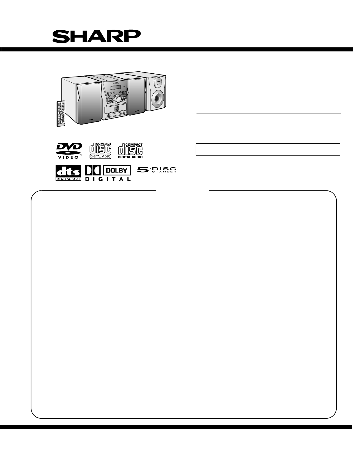
XL-DV60 DVD Micro System consisting of XL-DV60 (main
unit), CP-DV60F (front speakers) and CP-DV60SW(subwoofer).
• In the interests of user-safety the set should be restored to its original condition and only parts identical to those specified be used.
[4] SCHEMATIC DIAGRAM MAIN/POWER
AMP............................................................... 6-3
[5] SCHEMATIC DIAGRAM TUNER .................. 6-5
[6] SCHEMATIC DIAGRAM DISPLAY................ 6-7
[7] SCHEMATIC DIAGRAM DVD1/3 .................. 6-9
[8] SCHEMATIC DIAGRAM DVD2/3 ................ 6-11
[9] SCHEMATIC DIAGRAM DVD3/3 ................ 6-13
[10] WIRING SIDE OF PWB ............................. 6-15
[11] WIRING SIDE OF PWB MAIN TOP/POW-
ER AMP./JACK............................................ 6-17
[12] WIRING SIDE OF PWB MAIN BOTTOM...... 6-19
[13] WIRING SIDE OF PWB TUNER ................. 6-21
[14] WIRING SIDE OF PWB DISPLAY/
SWITCH ...................................................... 6-23
[15] WIRING SIDE OF PWB DVD TOP ............. 6-25
[16] WIRING SIDE OF PWB DVD BOTTOM...... 6-27
[17] WIRING SIDE OF PWB VIDEO TERMI-
NAL ............................................................. 6-29
CHAPTER 7. FLOWCHART
[1] TROUBLESHOOTING .................................. 7-1
XL-DV60
CHAPTER 5. CIRCUIT DESCRIPTION
[1] VOLTAGE .......................................................5-1
CHAPTER 6. CIRCUIT SCHEMATICS AND PARTS
LAYOUT
[1] NOTES ON SCHEMATIC DIAGRAM .............6-1
[2] TYPES OF TRANSISTOR AND LED .............6-1
[3] SCHEMATIC DIAGRAM VIDEO TERMI-
NAL.................................................................6-2
SHARP CORPORATION
CHAPTER 8. OTHERS
[1] FUNCTION TABLE OF IC............................. 8-1
[2] FL DISPLAY .................................................. 8-5
Parts Guide
This document has been published to be used
for after sales service only.
The contents are subject to change without notice.
Page 2
XL-DV60
Home StereoXL-DV60Service ManualXLDV60 Service ManualMarketE
CHAPTER 1. GENERAL DESCRIPTION
[1] PRECAUTION FOR USING LEAD-FREE SOLDER
1. Employing lead-free solder (From Serial No. 503040001)
"MAIN,TUNER,DISPLAY,
The LF symbol indicates lead-free solder, and is attached on the PWB and service manuals. The alphabetical character
following LF shows the type of lead-free solder.
Example:
2. Using lead-free wire solder
When fixing the PWB soldered with the lead-free solder, apply lead-free wire solder. Repairing with conventional lead wire solder
may cause damage or accident due to cracks.
As the melting point of lead-free solder (Sn-Ag-Cu) is higher than the lead wire solder by 40 C, we recommend you to use a
dedicated soldering bit, if you are not familiar with how to obtain lead-free wire solder or soldering bit, contact our service station
or service branch in your area.
3. Soldering
As the melting point of lead-free solder (Sn-Ag-Cu) is about 220 C which is higher than the conventional lead solder by 40 C,
and as it has poor solder wettability, you may be apt to keep the soldering bit in contact with the PWB for extended period of
time. However, Since the land may be peeled off or the maximum heat-resistance temperature of parts may be exceeded,
remove the bit from the PWB as soon as you confirm the steady soldering condition.
Lead-free solder contains more tin, and the end of the soldering bit may be easily corrected. Make sure to turn on and off the
power of the bit as required.
If a different type of solder stays on the tip of the soldering bit, it is alloyed with lead-free solder. Clean the bit after every use
of it.
When the tip of the soldering bit is blackened during use, file it with steel wool or fine sandpaper.
VIDEO TERMINAL
Indicates lead-free solder of tin, silver and copper.
,JACK,
SWITCH,DVD,POWER AMP.
,PWB" of this model employs lead-free solder.
Be careful when replacing parts with polarity indication on the PWB silk.
Lead-free wire solder for servicing
Ref No.
PWB-A DCEKKV521SJ03
PWB-B DCEKNV521SJ03
PWB-C DCEKDV521SJ03
PWB-D DCEKSV521SJ03
Parts No.
Main(A1)/Tuner(A2)
DISPLAY(B1)/Video Terminal(B2)/Jack(B3)/Switch(B4)
DVD
Power Amp.
Description
1 – 1
Page 3
FOR A COMPLETE DESCRIPTION OF THE OPERATION OF THIS UNIT, PLEASE REFER
TO THE OPERATION MANUAL.
[2] IMPORTANT SERVICE NOTES (FOR
U.S.A. ONLY)
BEFORE RETURNING THE AUDIO PRODUCT
(Fire & Shock Hazard)
Before returning the audio product to the user, perform the following
safety checks.
1. Inspect all lead dress to make certain that leads are not pinched or
that hardware is not lodged between the chassis and other metal
parts in the audio product.
2. Inspect all protective devices such as insulating materials, cabinet,
terminal board, adjustment and compartment covers or shields,
mechanical insulators etc.
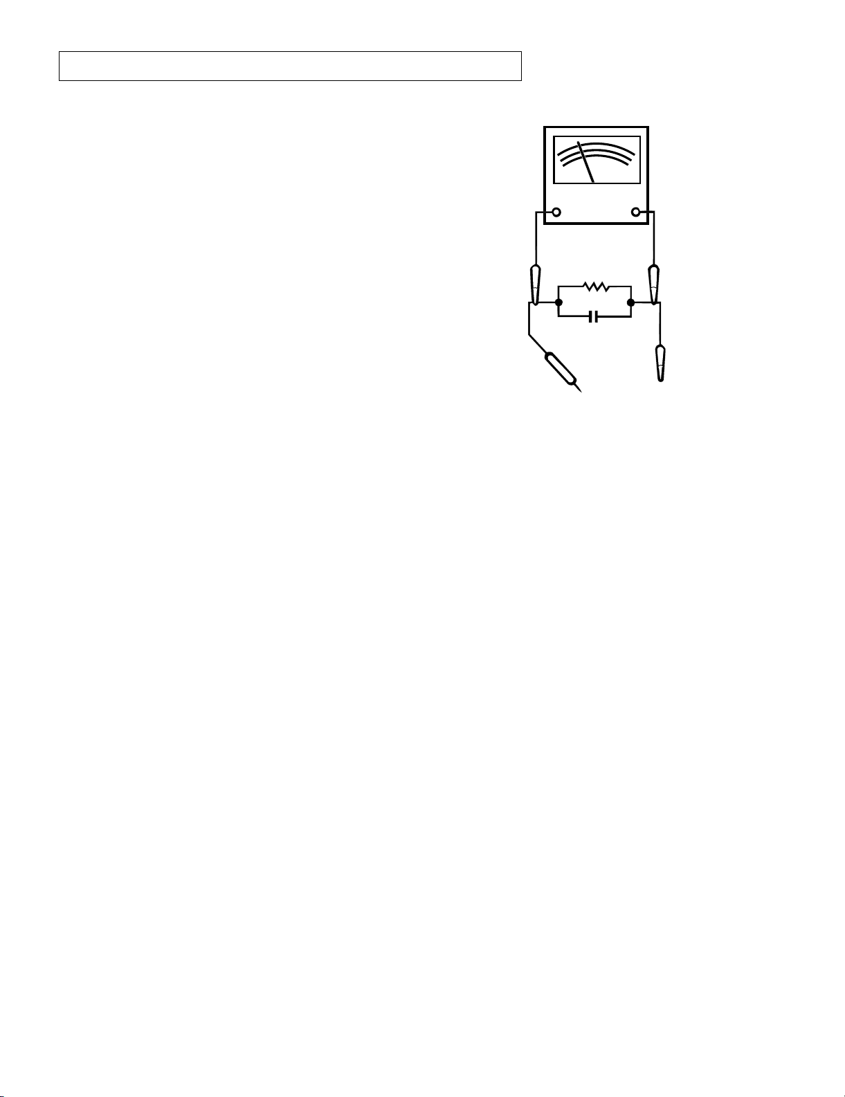
3. To be sure that no shock hazard exists, check for leakage current in
the following manner.
* Plug the AC line cord directly into a 120 volt AC outlet.
* Using two clip leads, connect a 1.5k ohm, 10 watt resistor paral-
leled by a 0.15µF capacitor in series with all exposed metal cabinet
parts and a known earth ground, such as conduit or electrical
ground connected to earth ground.
* Use a VTVM or VOM with 1000 ohm per volt, or higher, sensitivity
to measure the AC voltage drop across the resistor (See diagram).
* Connect the resistor connection to all exposed metal parts having a
return path to the chassis (antenna, metal cabinet, screw heads,
knobs and control shafts, escutcheon, etc.) and measure the AC
voltage drop across the resistor.
TO EXPOSED
METAL PARTS
All check must be repeated with the AC line cord plug connection
reversed.
Any reading of 0.3 volt RMS (this corresponds to 0.2 milliamp. AC.) or
more is excessive and indicates a potential shock hazard which must
be corrected before returning the audio product to the owner.
VTVM
AC SCALE
1.5k ohms
10W
0.15 µ F
TEST PROBE
XL-DV60
CONNECT TO
KNOWN EARTH
GROUND
1 – 2
Page 4
XL-DV60
[3] SPECIFICATIONS
■ General
Power source AC 120 V, 60 Hz
Power consumption 116 W
Dimensions Width: 6-5/16" (160 mm)
Weight 12.3 lbs. (5.6 k g)
Height: 9-7/16" (240 mm)
Depth: 12-9/16" (319 mm)
■ Amplifier
Output power Front speakers: 37.5 watts minimum RMS
Audio output
terminals
Audio input
terminals
Video output
terminals
per channel into 6 ohms from 100 Hz to 20
kHz, 10% total harmonic distort ion
Subwoofer: 45 watts minimum RMS into 6
ohms from 70 Hz to 130 Hz, 10% total
harmonic distortion
Front speakers and subwoofer: 6 ohms
Headphones: 16 - 50 ohms
(recommended: 32 ohms)
Optical digital output: Square type 1
Video/Auxiliary (audio signal): 500 mV/47 k
ohms
Video output: RCA type 1
S-video output: S-terminal 1
Component video output: RCA type 3
(Pr/Cr, Pb/Cb, Y)
■ DVD player
Type 5-disc multi-play compact disc player
Signal readout NTSC color
Supported disc
types
Video signal Horizontal resolution: 500 lines
Audio signal Frequency
DVD (region number 1, ALL), video CD,
audio CD, CD-R, CD-RW
S/N ratio: 75 dB
characteristics
S/N ratio CD: 95 dB (1 kHz)
Dynamic
range
Total harmonic distortion ratio
Linear PCM DVD: 30 Hz to
20 k Hz (sampling rate: 48
kHz)
30 H z to 20 kHz
(sampling rate: 96 kHz)
CD: 30 Hz to 20 kHz
Linear PCM DVD: 92 dB
CD: 92 dB
0.14 %
■ Tuner
Frequency range FM:87.5-108MHz
AM: 530 - 1,720 kHz
■ Front speaker
Type 2-way type speaker system
Maximum input
power
Rated input power 37.5 W
Impedance 6 ohm s
Dimensions Width: 6-1/2" (165 mm)
Weight 5.1 lbs. (2.3 kg)/each
(magnetic shield)
1-9/18" (4 cm) semi dome tweeter
4" (10 cm) woofer
75 W
Height: 9- 7/16" (240 mm)
Depth: 9-3/8" (238 mm)
■ Subwoofer
Type Subwoofer system (m agnetic shield)
Maximum input
power
Rated input power 45 W
Impedance 6 ohm s
Dimensions Width: 6-5/16" (160 mm)
Weight 7.3 lbs. (3.3 kg)
5-1/8" (13 cm) woofer
90 W
Height: 9- 7/16" (240 mm)
Depth: 11-1/4" (285 mm)
Specifications for this model are subject to change without prior
notice.
1 – 3
Page 5
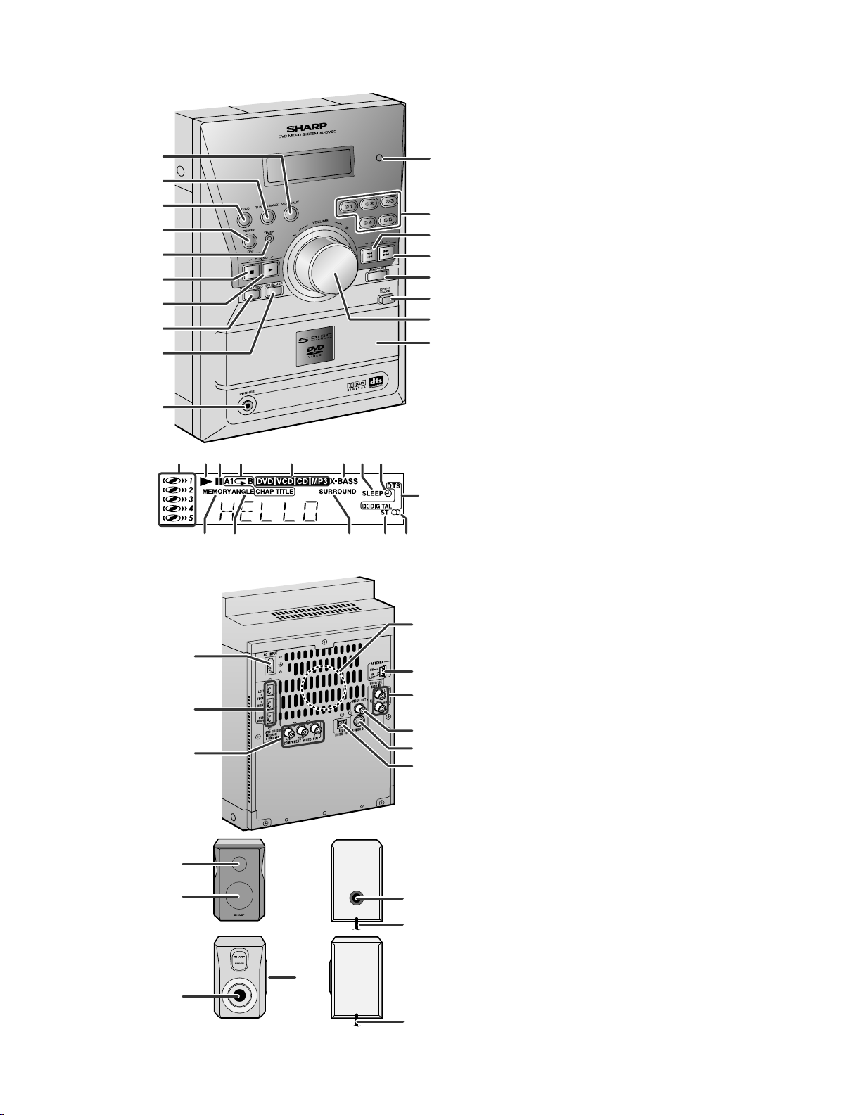
[4] NAMES OF PARTS
1
2
3
4
5
6
7
8
9
10
321 4 5678
XL-DV60
■ Front panel
1. Video/Auxiliary Button
2. Tuner (Band) Button
3. DVD/CD Button
11
12
13
14
15
16
17
18
9
13 1410 11 12
4. Power On/Stand-by Button
5. Timer Indicator
6. Stop or Tuning Down Button
7. Play or Tuning Up Button
8. Extra Bass/Demo Mode Button
9. Equ a lizer Mode S elect Button
10. Head p hon e Jack
11. Remote Sensor
12. Di sc Number Select Buttons
13. Chap ter (Track) Skip Down or Fast Reverse,
Tuner Preset Down Button
14. Chap ter (Track) Skip Up or Fast Forward,
Tuner Preset Up Button
15. Memory/Set Button
16. Disc Compartment Open/Close Button
17. Volume Control
18. Di sc Compartment
■ Display
1. Di sc Number Indicators
2. Play Indicator
3. Pause Indicator
4. Repeat Play Indicators
5. Disc Type Indicators
6. Extra Bass Indicator
7. Sleep Indicator
8. T ime r Play Indicator
9. Sound Mode Indicators
10. Memory Indicator
11. Angle Indicator
12. Surround Mode Indicator
13. FM Stereo Mode Indicator
14. FM Stereo Receiving Indicator
■ Rear panel
1. AC Power Input Jack
2. Speaker Terminals
4
1
5
6
3. Component Video Output Jacks
4. Cooling Fan
5. FM/AM Loop Antenna Jack
6. Video/Auxiliary (Audio Signal) Input Jacks
7. Video Output Jack
8. S-video Output Jack
9. Optical Digital Audio Output Jack
2
7
3
8
9
■ Front speaker
1
2
3
1. Semi Do me Tweeter
2. Woofer
3. Bass Reflex Duct
4. Speaker Wire
4
■ Subwoofer
2
1
1. Sub Duct Pipe
2. Subwoofer
3. Speaker Wire
3
1 – 4
Page 6
XL-DV60
10
11
12
13
14
15
16
17
18
1
2
19
3
20
4
21
5
6
7
8
9
22
23
24
25
26
27
28
29
30
31
32
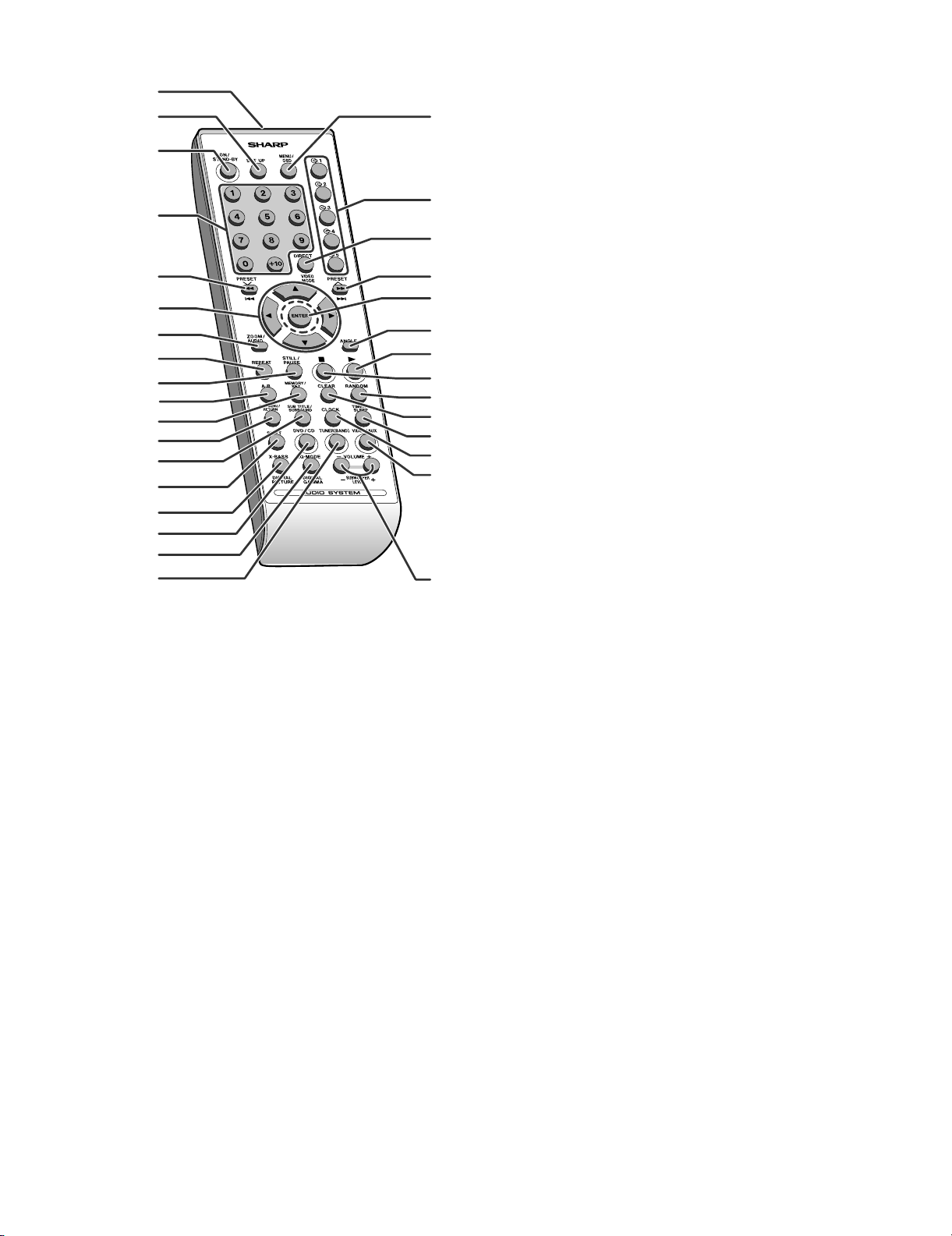
■ Remote control
1. Remote Control Transmitter
2. DVD Setup Button
3. Power On/Stand-by Button
4. Direct Number Buttons
5.Chapter(Track)SkipDownorFastReverse,
Tuner Preset Down, Time Down Button
6. Cursor Buttons
7. Zoom or Audio Select Button
8. Repeat Play Button
9. Frame Advance or Pause Button
10. A - B Repeat Button
11. Memory/Set Button
12.TopMenuorReturnButton
13. Subtitle or Surround Mode Select Button
14. Shift B utton
15. Extra Bass or Digital Picture Select Button
16. DVD/CD Button
17. Equ alizer Mode S elect or Digital Gamma Button
18. Tuner (Band) Button
19. Menu or On Screen Display Select Button
20. Di sc Number Select Buttons
21. Direct or Video M ode Select Button
22. Chap ter (Track) Skip Up or Fast Forward,
Tuner Preset Up, Time Up Button
23. Enter Button
24. An g le Select Button
25. Play Button
26. Stop Button
27. Random Button
28. Clear Button
29. T imer/Sleep Bu tto n
30. C l ock Button
31. Video/Auxiliary Button
32. Volume or Subwoofer Level Up and Down Buttons
1 – 5
Page 7
XL-DV60
CHAPTER 2. ADJUSTMENTS
Service Manual
XL-DV60
TUNER PWB-A2
[1] ADJUSTMENT
1. TUNER SECTION
fL: Low-range frequency
fH: High-range frequency
• AM IF/RF
Signal generator: 400 Hz, 30%, AM modulated
Test Stage Frequency Frequency
Display
IF 450 kHz 1,602 kHz T351 *1
AM Band
— 530 kHz (fL): T306
Coverage
AM Tracking 990 kHz 990 kHz T302 *3
*1. Input: IC303 21Pin Output: IC303 23Pin
*2. Input: Input is not connected Output: TP-VT(TP301)
*3. Input: Antenna Output:IC303 23Pin
• Check FM VT
Signal generator: 1 kHz, 40 kHz dev., FM modulated
Frequency Display Check
Point
87.5 MHz 87.5 MHz 3.4V ± 1.0V TP301
108 MHz 108 MHz 7.8V ± 1.0V TP301
• FM Mute Level
Signal generator: 1 kHz, 40 kHz dev., FM modulated
Frequency Display Adjusting
Parts
98.00 MHz
98.00 MHz VR351 Input: Antenna
(30 dBµV)
• FM Detection
Signal generator: 10.7 MHz FM sweep generator
Setting/
Adjusting
Connection
Parts
*2
1.1 ± 0.1 V
Instrument
Connection
Instrument
Connection
Output: Speaker Terminal
Instrument
20
IC302
TP301
L302
FM RF
1
T302
C393
IC301
AM
Tracking fL
CNP301
R356
IC303
R357
TP302
T351
AM IF
VR351
FM MUTE
LEVEL
18
R350
T306
AM BAND
COVERAGE fL
T304
FM IF
L303
FM OSC.
Figure 1 ADJUSTMENT POINTS
2. DVD/CD SECTION
• Adjustment
Since this DVD/CD system incorporates the following automatic
adjustment functions, readjustment is not needed when replacing
the pickup. Therefore, different PWBs and pickups can be combined freely.
Each time a disc is changed, these adjustments are performed
automatically. Therefore, playback of each disc can be performed
under optimum conditions.
Test
Stage
Frequency Frequency
Display
Setting/
Adjusting
Instrument
Connection
Parts
FM IF 10.7 MHz 98.00 MHz T304 Input: Pin 1 of
IC301
Output: Pin 18
of IC303
• FM RF
Signal generator: 1 kHz, 75 kHz dev., FM modulated
Test
Stage
Frequency Frequency
Display
Setting/
Adjusting
Instrument
Connection
Parts
FM OSC. — 87.50 MHz (fL): L303
*1
3.4 ± 0.1 V
FM RF 98.00 MHz
98.00 MHz L302 *1
(10 ~ 20dB)
*1. Input: Antenna Output: 18 Pin of IC303
2 – 1
Page 8
XL-DV60
[2] TEST MODE
The test mode applied to this microcomputer has three modes, namely
the ordinary test mode for adjustment or measurement, the aging test
mode, and the self-diagnosis test mode for self-judgment in case of
final product inspection.
• The TUNER TEST 2 mode is obtained with >> + MEMORY/SET +
POWER ON/STAND-BY. ->Turn off AC in the TEST 2 mode to
restore the initial state.
1. Turning on the test mode
For obtaining each test mode, press the Power ON/STAND BY button,
while keeping pressing the following two buttons in the ordinary standby mode (power off). In this case, the main unit buttons are valid.
When turning the POWER on with remote control buttons, test modes
are not obtained.
[Ordinary test mode]
1. Tuner Test Mode (TEST 2).......................................................
TUNER(BAND) + DISC1
2. Electronic Volume Test Mode (TEST 3)...................................
TUNING DOWN + VOLUME UP
3. Timer Test Mode (TEST 4).......................................................
TUNING UP + DISC5
4. FL Test Mode (TEST 5)...........................................................
PRESET DOWN + VOLUME DOWN
5. DVD MECHANISM Aging Test Mode (TEST 8).......................
DVD/CD + Equalizer
[Self-diagnosis Test Mode]
1. Button input diagnosis test mode (TEST 6)..............................
PRESET UP + DISC5
Processes are different depending on destinations at initial settings.
2. Tuner Test Mode (TEST 2)
1. Outline of tuner (radio) test mode
The tuner test mode is intended to store the adjustment and measurement frequencies in the preset memory CH. When adjusting
the tuner section in the production line, adjusting personnel are not
required to set frequency.
2. Details of tuner test mode
Press the "TUNER(BAND)" button and "VOLUME UP" jog in
POWER OFF state and turn on the power by the use of "POWER
ON/STAND BY" button to preset and store frequency for adjustment and measurement of destination specified by the AREA terminal in the preset memory CH. However, Ordinary 1 and Ordinary 2
are stored in the destinations when the test mode is obtained.
(As for frequencies to be preset and stored for each destination, refer
to item 3.)
The tuner test mode is started from preset No.1.
The operations of test mode are identical with the ordinary operations
of TUNER function. FUNCTION switching is invalid.
It is necessary to discard the content of preset memory when the tuner
test mode is ended; be sure to write "0000" or "1111" bits in the memory to be checked for judging memory error at initial setting and to initialize memory.
When the tuner test mode is obtained, the following display lights for
one second.
Turn off POWER to protect the memory of TEST 2 mode.
Turn off POWER again to obtain the ordinary operation while the
data is stored in the memory (besides TUNER).
If AC OFF state is maintained in this state for about 1/2 day, start is
executed in the initial state.
• To clear the whole memory, insert the AC cord, pressing MEMORY/SET + PLAY.
3. Preset frequencies for various destinations
(random preset memory)
CH BAND FM
1
2
FM STEREO
3
4
5
CH BAND FM
6
7
AM
8
9
10
CH BAND FM
16-35 ——————
36
37
FM MONO
38
39
40
• The slant line sections of the table store no memory.
FM 87.5 MHz
FM108.0 MHz
FM 98.0 MHz
FM 90.0 MHz
FM106.0 MHz
AM 530 kHz
AM1720 kHz
AM 990 kHz
AM 600 kHz
AM1400 kHz
FM106.0 MHz
FM 90.0 MHz
FM 98.0 MHz
FM108.0 MHz
FM 87.5 MHz
3. Electronic volume Test Mode (TEST 3)
When this test mode is obtained, the following display lights for one
second.
In this mode, volume is Volume -14 dB (STEP 23), FLAT AND X-BASS
ON, and start-up function to DVD/CD, respectively. The button operations in the test mode are the same as those of ordinary operation
except volume UP/DOWN.
1) The display is the same as that of ordinary operation except test
mode setting.
2) Unlike the ordinary state, the volume is controlled with the volume
UP/DOWN jog in accordance with the following three steps.
Vol ume - ∞ (STEP 0) <-> Volume-14 dB (STEP 23) <-> Volume-0
(STEP 30)
3) X-BASS is switched when button is pressed.
2 – 2
Page 9
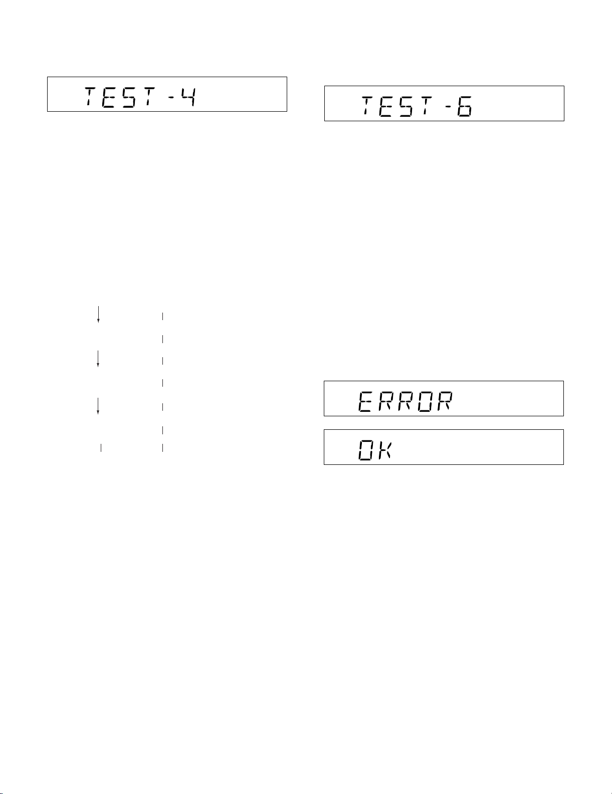
4. Timer test Mode (TEST 4)
When this test mode is obtained, the following display lights for one
second.
Set the current time and timer time according to the following procedure to reproduce the timer.
1. Set the current time to 1:00, the timer to ON time 1:05, the function
to DVD/CD, and volume to STEP 12, respectively. One minute is
counted as one second, and the timer is reproduced. The fade-in
(when playback is started) is executed at a rate of one step for 1
sec. After completion of fade-in, the fade-out is executed at a rate
of one step for 1 sec (WAIT 1 sec inserted).
After completion of fade-out, the power is turned off (after WAIT 1
sec), and the mode is shifted to the standby.
The display during operation is the same as that of ordinary timer
operation.
5. FL Test Mode (TEST 5)
When the FL test mode is obtained, all the FL segments are lighted.
Then pressing the "PLAY" button switches display as below.
————–
Lighting of all segments
XL-DV60
6. Button input diagnosis Test Mode (TEST 6)
When the test mode is obtained, the following is displayed.
(STAND-BY AND DEMO OFF STATUS)
This test mode is intended to check whether all the main unit buttons
can be detected. Accordingly, in this test mode, it is checked whether
the "POWER ON/STAND BY" button was pressed after all the buttons
shown below were pressed. If the result is OK, OK is displayed. If any
one of keys was not pressed, an error is displayed. In both cases of
OK termination or error termination, the mode is shifted to the standby
mode if the "POWER ON/STAND BY" button is pressed subsequently.
All models using this type of microcomputer are not always provided
with the same buttons. Since the buttons used are different depending
on models, types of buttons to be used are determined by whether
SURROUND, and an electric lid are available at the initial setting by
MODEL port.
The order of buttons to be pressed is not determined. Accordingly, it is
checked whether all buttons have been pressed.
1. PU-IN buttons: REW/PRESET DOWN + STOP
Since this model is provided with SURROUND (HAVE OR NOT),
and electric DVD/CD lid, the following 10 buttons are detected as
all buttons.
PLAY, X-BASS/DEMO, FUNCTION, VOLUME UP/DOWN, MEMORY/SET, REW, FF, STOP, DVD/CD-OPEN/CLOSE
The OK/ERROR display of test result is as follows.
Lighting of odd segments
Lighting of even segments
__________
2 – 3
Page 10
XL-DV60
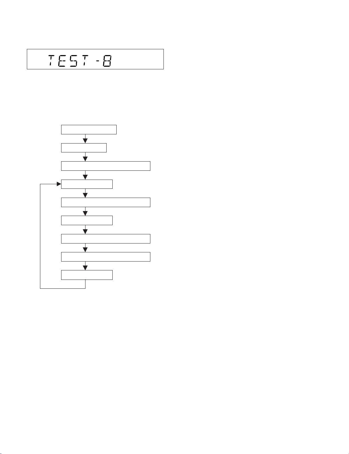
7. DVD MECHANISM Aging Test Mode (TEST 8)
OPEN/CLOSE & 5 DISC CHANGER aging test.
DISPLAY:
FUNCTION:
Enter the TEST MODE 8, MCU control the 5 DISC CHANGER OPEN/
CLOSE. After open finished, tray rotate 1 circle (360 degree). Then
close, After close finished, tray rotate 1 circle (360 degree) again.
Request:
Every period include 4 operation. Below is TIMING:
Enter test mode
CHANGER
Find the disc 1 position
open
delay 3S after open finish
rotate 1 circle
close
delay 3S after close finish
rotate 1 circle
2 – 4
Page 11
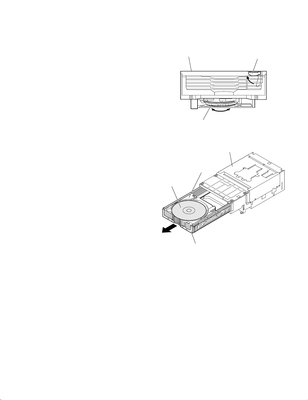
DVD Changer
Unit
DVD/CD Disc
Carriage
Drawer
Home StereoXL-DV60Service ManualXLDV60 Service ManualMarketE
CHAPTER 3. MECHANICAL DESCRIPTION
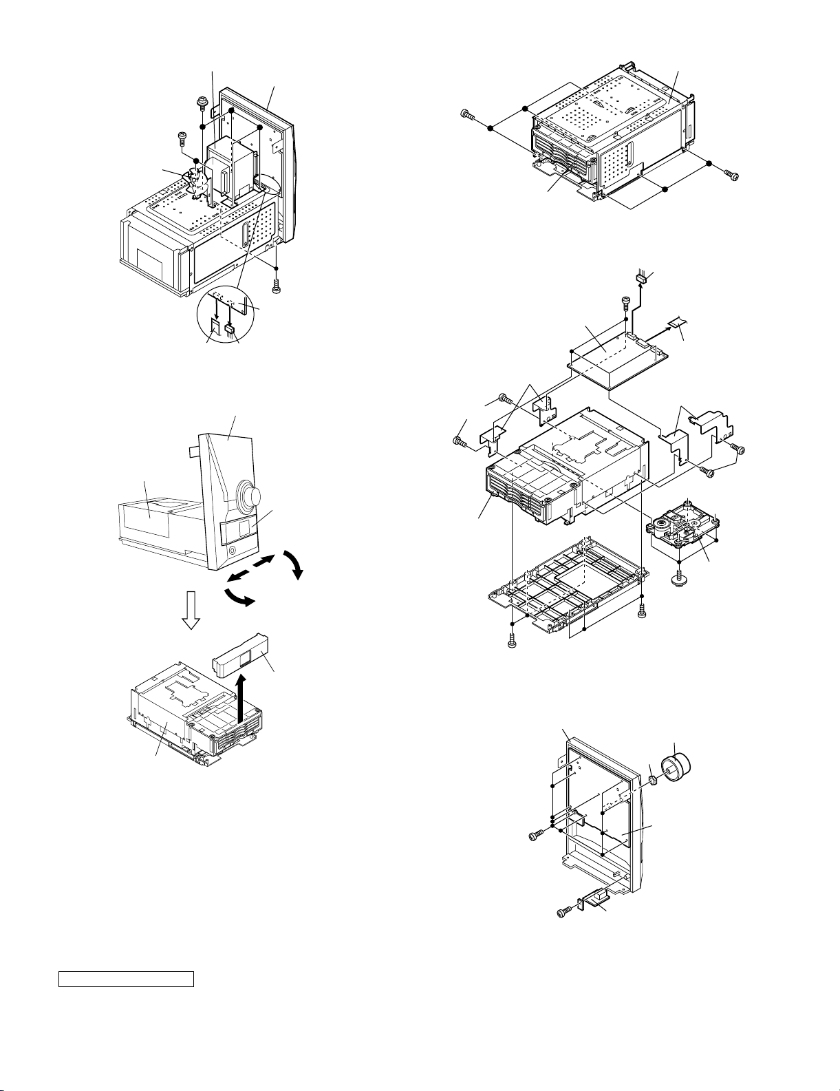
[1] REMOVING AND REINSTALLING THE MAIN PARTS
1. How to remove DVD/CD Disc manually (See Fig.
1,2)
Perform steps 1 to 9 of the disassembly method to remove the DVD
Changer unit.(see page 3-2,3-3)
1. Rotate the gear cam until the arm switch C becomes the position of
the Figure 1.
2. Pull the drawer to the front like the Figure 2.
And the DVD/CD disc on the carriage is taken out.
DVD Changer
Unit
XL-DV60
Arm switch C
Gear cam
Figure 1
Figure 2
3 – 1
Page 12
XL-DV60
(A1) x2
ø3x8mm
(A1) x2
ø3x8mm
(B1) x2
ø3x8mm
(B1) x2
ø3x12mm
(B1) x2
ø3x10mm
(B1) x2
ø3x8mm
(A1) x1
ø3x8mm
Top Cabinet
Side Panel
(Left)
Side Panel
(Right)
Rear
Panel
(E1) x1
ø3x12mm
(F1) x1
ø3x6mm
(E1) x2
ø3x6mm
(E2) x2
(E2) x1
(E2) x1
Main PWB
Power Amp.
PWB
(E2) x1
(E2) x3
(E2) x2
Front Panel
(F1) x3
ø3x6mm
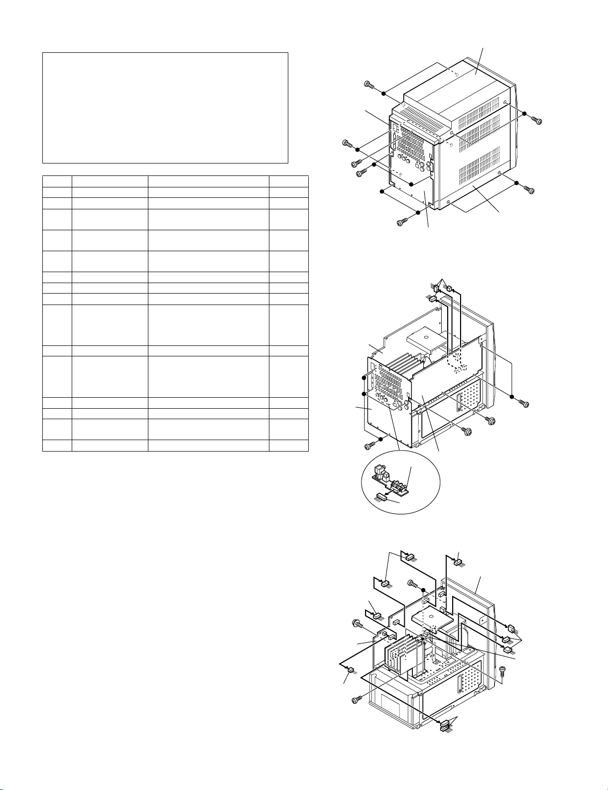
[2] DISASSEMBLY
Caution on Disassembly
Follow the below-mentioned notes when disassembling the unit and
reassembling it, to keep it safe and ensure excellent performance:
1) Be sure to remove the power supply plug from the wall outlet
before starting to disassemble the unit.
2) Take off nylon bands or wire holders where they need to be
removed when disassembling the unit. After servicing the unit,
be sure to rearrange the leads where they were before disassembling.
3) Take sufficient care on static electricity of integrated circuits and
other circuits when servicing.
STEP REMOVAL PROCEDURE FIGURE
1 Top Cabinet 1. Screw.........................(A1) x 5 1
2 Side Panel 1. Screw.........................(B1) x 8 1
3 Rear Panel 1. Screw........................(C1) x 6
2. Socket.......................(C2) x 1
4 Tuner PWB 1. Screw........................(D1) x 3
2. Socket.......................(D2) x 3
5 Main PWB 1. Screw.........................(E1) x 3
2. Socket.....................(E2) x 10
6 Power Amp.PWB 1. Screw.........................(F1) x 4 3
7 Transformer 1. Screw........................(G1) x 4 4
8 Fan Motor 1. Screw........................(H1) x 2 4
9 Front Panel/DVD
Tray Cover
1. Screw.........................(J1) x 2
2. Flat cable...................(J2) x 1
3. Socket........................(J3) x 1
4. DVD Tray cover..........(J4) x 1
10 Chassis 2. Screw........................(K1) x 6 6
11 DVD PWB
(Note 1)
1. Flat cable...................(L1) x 1
2. Socket........................(L2) x 1
3. Screw.........................(L3) x 4
4. Screw.........................(L4) x 4
12 DVD Changer Unit 1. Screw........................(M1) x 6 7
13 DVD Mechanism 1. Screw........................(N1) x 4 7
14 Display PWB 1. Knob.........................(P1) x 1
2. Screw......................(P2) x 10
15 Jack PWB 1. Screw........................(Q1) x 1 8
Note 1:
After removing the connector for the optical pickup from the connector,
wrap the conductive aluminium foil around the front end of the connector so as to protect the optical pickup from electrostatic damage.
2
2
3
4
5
7
8
Main PWB
Rear
Panel
(C1) x5
ø3x10mm
Video Terminal
PWB
(C2) x1
Figure 1
(D2) x3
(C1) x1
ø3x12mm
Tuner PWB
(D1) x2
ø3x6mm
(D1) x1
ø3x12mm
Figure 2
Figure 3
3 – 2
Page 13
(H1) x2
(K1) x3
ø3x8mm
(K1) x3
ø3x8mm
DVD Changer
Unit
Chassis
(M1) x3
ø3x8mm
(M1) x3
ø3x8mm
(N1) x4
ø2.5x10mm
(L3) x4
ø3x6mm
(L4) x2
ø3x6mm
(L4) x2
ø3x6mm
Bracket
(L1) x1
(L2) x1
DVD Changer
Unit
DVD PWB
DVD Mechanism
Bracket
(P2) x10
ø2.5x8mm
(Q1) x1
ø2.5x8mm
(P1) x1
Nut
Front Panel
Display PWB
Jack PWB
ø3x6mm
Fan Motor
Transformer
(G1) x4
ø4x10mm
(J2) x1 (J3) x1
Figure 4
Front Panel
Front Panel
(J1) x2
ø3x12mm
Display PWB
XL-DV60
Figure 6
DVD Changer
Unit
DVD Changer
Unit
Figure 5
DVD Tray Cover
DVD Tray Cover
(J4) x1
Figure 7
CP-DV60F, CP-DV60SW
These speaker CP-DV60F, CP-DV60SW are available in assembles
only and may not be disassembled.
Figure 8
3 – 3
Page 14
XL-DV60
+5V+B
+B
+B
+B
+B
+B
+B
+B
+B
+B
+B
+B
+B
+B
+B
+B
+B
+B
+B
+B
+B
+B
+B
+B
+B
+B
+B
+B
+B
+B
+B
3.3K
LM2576T
KIA7812API
31
KIA7805API
31
9
POWER TRANSFORMER
(MAIN)
8
7
6
5
4
3
2
1
2
2
+5.6V
+7V
3.15A 125V
GNDA
2A 125V
VCCA
VCC2
GNDRF
GND
VCC1
S12V
+10V
MGND
6.3A 125V
6.3A 125V
VF1
VF2
+B1
-B1
AGND
+B2
DGND
DGND
3.8V
3.8V
-30V
-B
-B
-B
-B
-B
D_GND
+5.6V
P_CON
NC
NC
VEE
VCC
+12V
GND
S/W
R_CH
A_GND
L_CH
1
4
7
3
2
5
6
1
7
5
2
6
4
8
3
2345
1234
5
4
6
2
3
1
7
1
TO TUNER PWB
FROM DVD PWB
FROM
DISPLAY PWB
A GND
A GND
VOLTAGE
REGULATOR
VOLTAGE REGULATOR
CNW602
CNS602
CNP807
R155
IC203
IC201
IC202
CNP101
D205
C211
D201
F201
F202
F204
C212
T201
F203
Q101
Q102
Q117
Q118
Q213
Q214
Q115
Q116
Q201
Q207 Q208
Q203
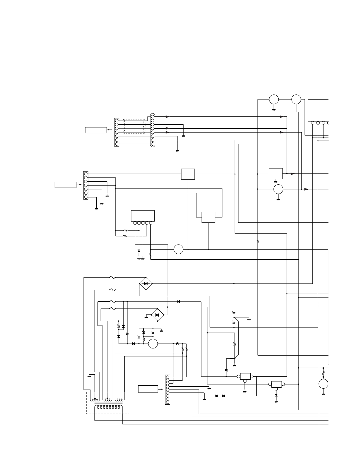
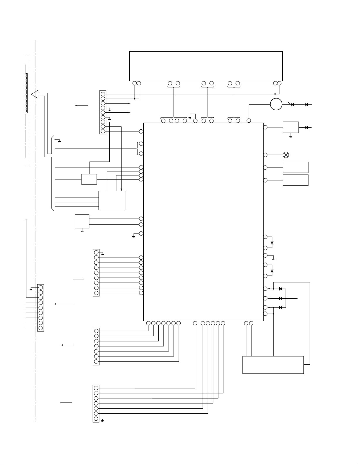
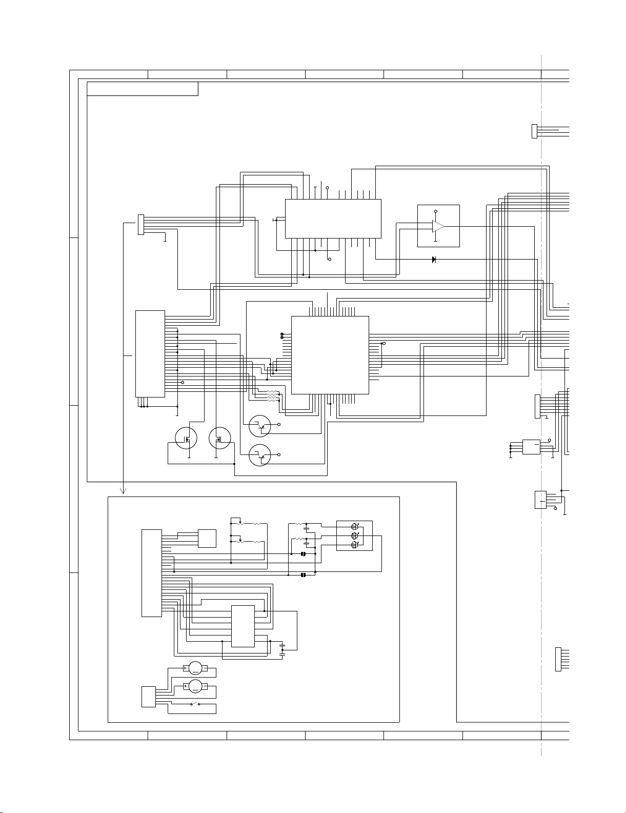
CHAPTER 4. DIAGRAMS
[1] BLOCK DIAGRAM MAIN
Figure 4-1 BLOCK DIAGRAM (1/6)
4 – 1
Page 15
+
IC101
LM4733TA
POWER AMP.
S/W_RF
MUTE3
GND
S/W_OUT
NC
R_RF
MUTE2
GND
NC
VEE
R_IN
R_OUT
L_RF
L_IN
MUTE1
GND
NC
VEE
L_OUT
NC
VCC
NC
NC
VEE
VCC
123456789101112131415161718192021222324252627
B +B
-B
VCC
-B
S/W_IN
+
-
+
-
+
-
SO101
SPEAKER TERMINAL
L-CH
FRONT SPEAKER
R-CH
SUB WOOFER
XL-DV60
RIN
ROUT
A_GND
LOUT
LIN
+B
L
+B
B
-B
Q107
Q108
R
RLY101
R158
Q110
RLY102
+B
Q111
R
L
Q112
Q113
Q114
+B
SUB_RELAY IN
SUB_RELAY OUT
SP_RELAY
SINGAL_LVL
FAN_START
SP_DETECT
P_MUTE
FAN_PRO
CD+B
CNP102
1
2
3
4
5
6
7
FROM DISPLAY PWB
1
3
11
10
2
9
8
7
6
5
4
JK101
HEADPHONES
Q109
T202
+B
+B
D214~217
POWER TRANSFORMER
(SUB)
LF201
LINE FILTER
Q203
M
M201(218-4)
Q205
IC204
AN78L05
CONSTANT VOLTAGE
REGULATOR
+B
31
2
RLY201
SO202
AC
SOCKET
Q206
+B
AC POWER
SUPPLY CODE
AC 120V 60Hz
Q204
Q202
FAN MOTOR
+B
Figure 4-2 BLOCK DIAGRAM (2/6)
4 – 2
Page 16
XL-DV60
M
C
D
J
D
C
S
F
D
D
S
C
C
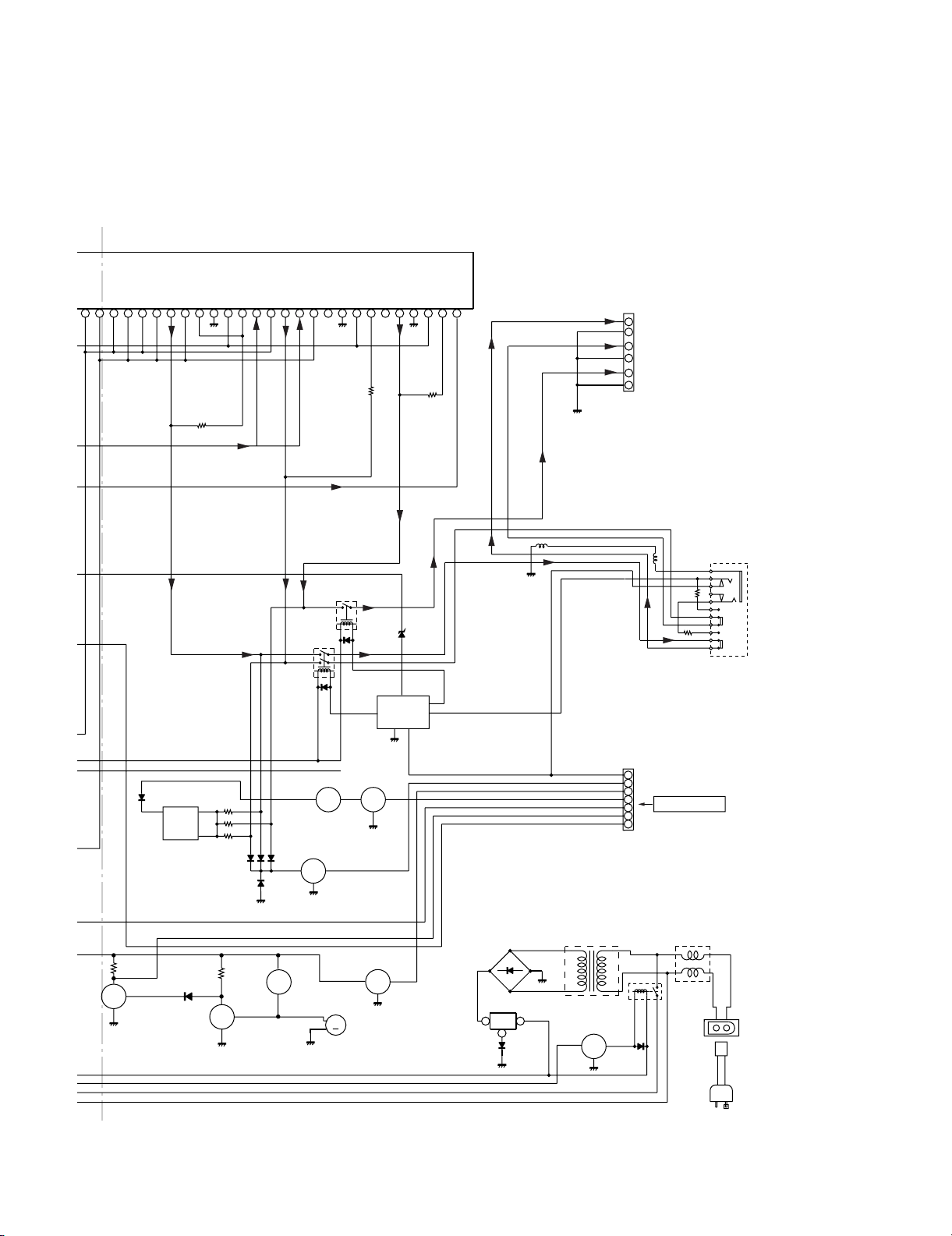
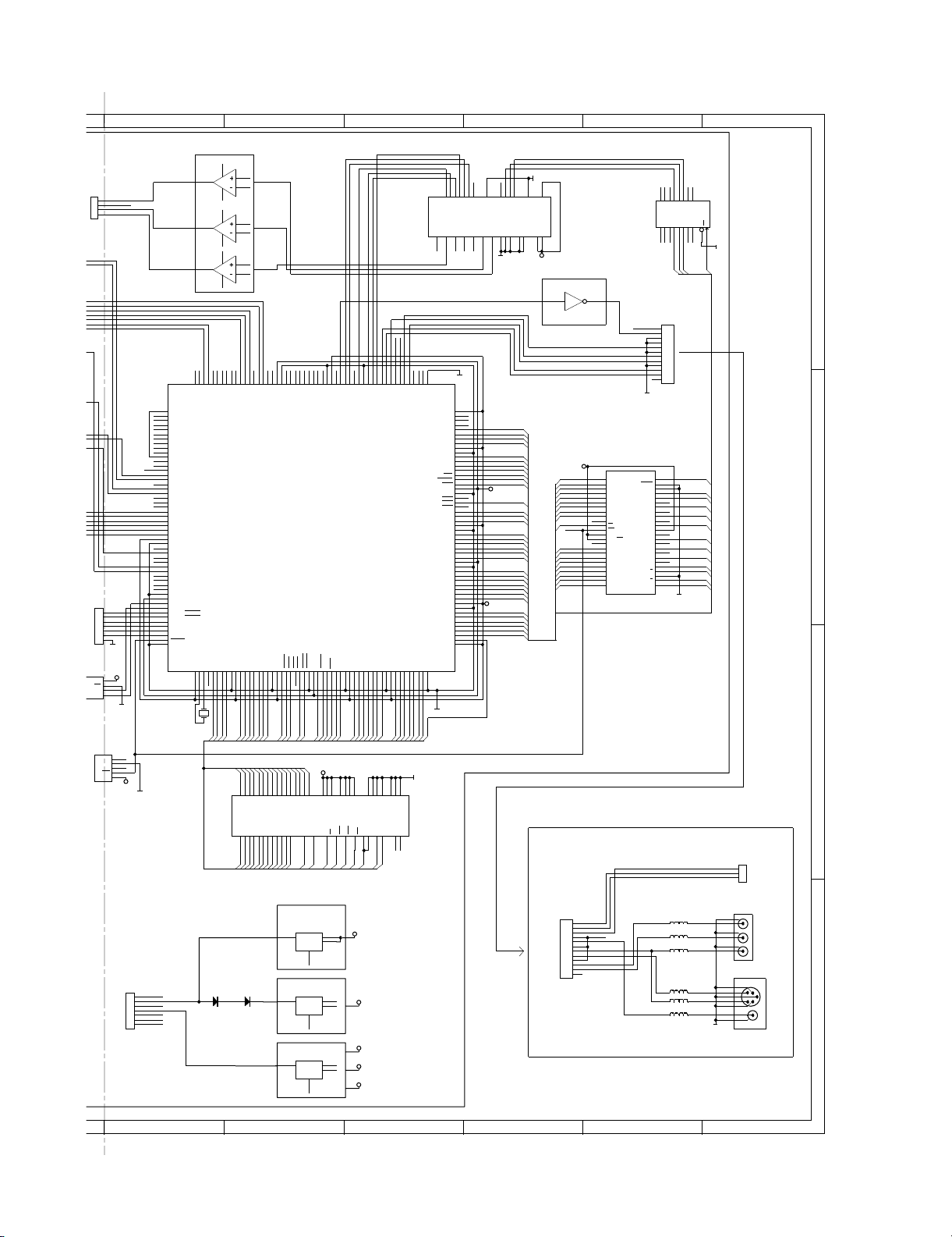
[2] BLOCK DIAGRAM TUNER/DISPLAY
+7V
+12V
D_GND
SW_CH
R-CH
A_GND
L-CH
CNP602
7
6
5
4
3
2
1
SO601
VIDEO/AUX
AUDIO IN
L-CH
R-CH
+B5
SW_CH
A_12V
+B5
8
IC602
1
NJM4558D
BUFFER AMP.
4
+7V
23
VDD
LC75341M
SIGNAL CONTROL
CLDICE
3
L/R OUT
214
IC603
DVD DECODER SECTION
L
R
1624 921
DVD/CD_SUB
1312
R
L
R
L
1411
+7V
24 21
AUX_L/R
L/R OUT
21423
L
R
IC601
VDD
LC75341M
SIGNAL CONTROL
CL
L
CE
TUN_L/R
R
169
DI
DVD/CD_L/R
1312
L
R
33
L
R
1411
MOTOR
SOLENOID
CE_WOOF
DI
CE
CL
CD CHANGER PWB ASS'Y
PHOTO
INTERRUPTER
M
D_GND
SW4
SW3
SW5
SW6
SW2
SW1
SW7
CD_PH2
CD_PH3
MM+
CD_SOL1
MM-
CD_SOL2
SW8
1
2
3
4
5
6
7
8
9
10
11
12
13
14
15
AM LOOP/FM
ANTENNA
CNP301
14
LA1832S
FM IF DET.
FM MPX./AM IF
DO
CL
DI
CE
A_12V
+B5
IC303
CNP302
1
2
3
4
5
6
7
8
9
TO
TO
IC301
TA7358AP
B.P.F
BF301
FM
3
2
AM
1
FM FRONT END
1
384
L302
FM RF
AM
TRACKING
T302 T306
FM OSC
+B6
7
5
L303
AM BAND
COVERAGE
FM IF
OSC
BUFF
Q302
FM+B
CF303 CF302T304
VT
SWITCHING
Q306
IC302
LC72131
PLL(TUNER)
+B5
Q360
450 kHz
T351
CF352
AM IF
21
OUT
AM MIX
IF OUT
21
10
AM OSC IN
AM OSC OUT
AM RF IN
X352
4.5 MHZ
20 22 11 12
AOUT
21
FM
1615
XIN
7
IF REQ
AM IN
FM IN
XOUT
CLK
DI
CE
FM
5413
6
6
9
7SD6
STEREO
IF IN
DO
4
AM IF
9810
10.7 MHz
CF351
98517
FM
DET
GND
FM+B
VCO
FM/AM
OUT
MPXIN
18
1215162324
Q351
17
MUTE
MO/ST
FM/AM
+B5
ZD351
5.1V
X351
456 kHz
13
L
MO/ST
R
FM/AM
Figure 4-3 BLOCK DIAGRAM (3/6)
4 – 3
Page 17
XL-DV60
0
1
2
3
4
5
VFD701
FL DISPLAY
VF2
CNS101
3.8V
1
VF1
3.8V
VF2
2
-30V
3
P_CON
Q502
Q503
Q511
-B2
D_GND
+5.6V
M_GND
+10V
+5.6V
4
5
6
7
8
9
+5.6V(MOTOR)
TO MAIN PWB
CNP101
D_GND
SW1~8
CD_PH3
CD_SOL1,2
3940
+5.6V(SYSTEM)
P_CON
6
SW1
64
~
~
SW8
71
CD_PH
73
MM+
74
MM-
75
CD_SOL
76
37 22
~
50
63
P20
47
52
~
~
~
~
P8
P9
21 18
~
4551
42
~
~
P5
P4
VP
14 4
~
40 30
~
~
P1
11G
1G
TIMER_LED
POWER_KEY
KEY2
KEY1
IRQ
VF1
112
LED701
Q705
REMOTE
SENSOR
29
20
19
18
RX701
SW709
POWER
ON/STAND-BY
KEY
SW710~SW717
KEY
SW701~SW708
+5.6V
(SYSTEM)
+5.6V
(SYSTEM)
CNP302
1
2
3
4
5
6
7
8
9
TO MAIN PWB
MM-
CD_PH2
MM+
D_GND
SUB_WOOF_SEL
CE_WOOF
SD
FM_ST
DO
CL
CE
DI
CNP102
SW700
VOLUME
JOG
D_GND
SUB_WOOF_SEL
CE_WOOF
FM_ST
SP_RELAY
SIGAL_LVL
FAN_START
SP_DETECT
P_MUTE
FAN_PRO
CD+B
SD
DO
CL
CE
DI
CNS302
1
2
3
4
5
6
7
8
9
CNS102
1
2
3
4
5
6
7
Q504~Q509
CHANGER
MOTOR
DRIVER
IC701
IXA009SJ
JOG_DOWN
77
JOG_UP
78
VSS2
89
2
SUB_WOOF_SEL
100
CE_WOOF
80
SD
79
FM_ST
91
DO
87
CL
85
CE
86
DI
FAN_PRO
FAN_START
SP_DETECT
SP_RELAY
SINGAL_LVL
88 94 927 8 23 83 9527 96 11 2697 98 99
P_MUTE
SYSTEM
MICROCOMPUTER
DVD_STB
CD+B
DVD DI
CF2
16
X702
15
14
13
12
17
90
46
72
RESET
X701
8MHz
32.768 kHz
+B3
CF1
VSS1
XT2
XT1
VDD1
VDD2
VDD3
CLID_OUT
DVD BUSY
DVD CLK
DVD DO
RESET
VDD4
SYS_STOP
Q702,Q703,Q704
TO DVD PWB
J5
DVD_STB
CLID_OUT
DVD BUSY
DVD CLK
DVD DI
DVD DO
D_GND
CNP802
1
2
3
4
5
6
7
Figure 4-4 BLOCK DIAGRAM (4/6)
4 – 4
Page 18
XL-DV60
T
A
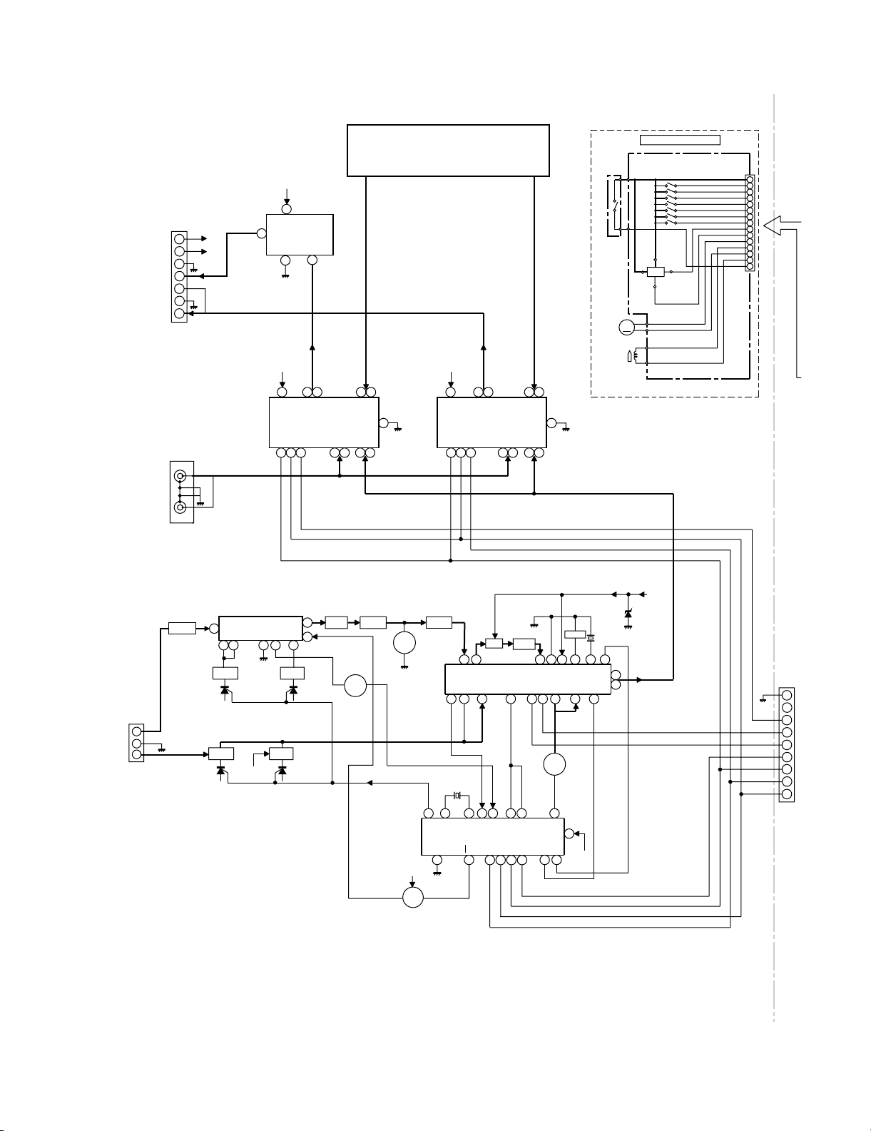
[3] BLOCK DIAGRAM DVD
DECODER SECTION
D
J4
LOAD-/DCMO-
1
LOAD+/DCMO+
2
SLED+
3
SLED-
4
5
6
CON6
MGND
JP1B
C
B
GND(NC)
GND(NC)
LD(CD)
(GND)
VR(CD)
GND(NC)
VR(DVD)
(GND)
LD(DVD)
(GND)
(VCC)
VS(VCC)
GND27GND28GND29GND
RFOUT
30
KHM-280 (JP26-0.5MM)
PICKUP UNIT ASS'Y
TRKTRK+
FCS-
FCS+
LD(780nm)
GND(780nm)
VR(780nm)
VR(650nm)
GND(650nm)
LD(650nm)
GND(PDIC)
VCC
KHM-280CN
A
DVD MECHANISM UNIT ASS'Y
SPINDLE+
SPINDLE-
SLED+
SLEDLIMIT_SW
LIMIT_SW
MOTOR_CN
TRACK-
26
TR-
TRACK+
25
TR+
24
FOCUS-
FO-
FOCUS+
23
FO+
22
21
CDLDO
20
19
VRCD
18
PD
17
PD
16
VRDVD
15
14
DVDLDO
13
12
B
B
11
E
E
10
D
D
9
C
C
8
7
H
6
G
G
A
5
A
4
RF50V
PVC
3
2
F
F
RFOUT
1
RFGND
3
Q12
2SK3018
2
1
RFGND
26
25
24
23
22
NC
21
NC
20
19
18
17
PD
16
NC
15
14
13
12
B
11
E
10
D
9
C
8
7
H
6
G
5
A
4
3
VC
2
F
1
RF
SPINDLE MOTOR
12
12
1
2
3
SLED MOTOR
4
5
6
SW-SPST
RFGND
A
Focus+Tracking tot a
must be 150mA RMS o
1
TRK+
2
TRK-
3
FCS-
4
FCS+
2-AX1S
M
M
R68 1K
R67 1K
R64 1K
R65 1K
Q11
2SB1132
4
3
1
Q13
2SK3018
2
1
Q10
2
2SB1132
4
2
1
0
6.8K
0
2.2K
7
VC6RF
8
9
10
11
12
5
H
G
4
C
B
3
D
A
2
E
F
1
GND
VCC
PH561L
Spindle Motor
Rated Voltage(DC): 3.0V (1.7-6.0);
Rated load: 0.392mN.m;
Current(At rated voltage and load): 105mA or less;
Sled Motor
Rated Voltage(DC): 3.0V (1.6-6.0);
Rated load: 0.392mN.m;
Current(At rated voltage and load): 92mA or less;
MGND
654321
J1
L_OUT
1
GNDA
2
TO TUNER PWB
MVCC
VCC
MGND
14
29
GND
30
GND
VOLD+
VOTK+
VOLD-
VOTK-
17
16
15
LOAD+/DCMO+
TRACK-
TRACK+
RFDC
1
DVDFRP
2
DVDRFN
3
A2
4
B2
5
C2
6
D2
7
CP
8
CN
9
D
10
C
11
B
12
A
13
CD_D
14
CD_C
15
CD_B
16
CD_A
CD_F
3
RF50V
3
RF50V
4.7
4.7
1uF
12
SHORT-LAND
12
SHORT-LAND
PD IC: PH561L
VCC: 4.5V-5.5V
VC: 2.2V-(VCC2
A,B,C,D: Focus Erro
E,F,G,H: Track Erro
RF: RF Output
0.1uF
0.1uF
VCC8PVCC19PGND10VOSL-11VOSL+12VOFC-13VOFC+
PVCC2
VNFTK
PGND
21
20
19
18
LOAD-/DCMO-
MVCC
RF50V
64
63
ATOP62ATON61AIN60AIP59VPA58RFAC57BYP56DIN55DIP54FNP53FNN52VNA
RFSIN
U7
ES6603S
RF AMP.
DVDPD
DVDLD
CDPD
CDLD
CD_E
VNB
VPB
17
18
19VC20
21
22
23
24
25
PD
PVC
CDLD
DVDLD
RF50V
1
1uF
4
SLD6261ALI
7
PREGND
VINLD
22
LDON
MIRR
26
27MP28MB29
LDON
MIRR
DVD_LD
CD_LDPDGND
SLEGN
CTKERR125CTKERR2
24
23
SPINDLE
51
49
MEV50RX
SDATA
MEVO
MLPF
MIN
30
31
32
VLD: 4.75V- 5
MNTR
SDEN
SCLK
FOCUS
MOTOR DRIVER
BA5954FP
2
U8
VINFC1CFCERR1
CFCERR23VINSL+4VINSL-5VOSL6VNFFC
LOAD-/DCMO-
VINTK
26
TRACK
V33
LCP
LCN
CE
FE
TE
PI
V25
V125
TPH
DFT
LINK
LOAD+/DCMO+
STBY
BIAS
28
27
SCSJ
48
47
SDATA
SCLK
46
45
RF33V
44
43
42
41
40
39
38
37
36
35
34
33
23
CEI
FEI
TEI
SBAD
U6A
TL3472
AMP.
MVCC
8
3
+
2
-
4
MGND
D6
RLS4148
1
TO DISPLAY PWB
GND
3
4
CON4
J5
1
2
3
4
5
6
7
CON7
U10
24C02
1
S0
VCC
2
S1
WC
3
S2
SCL
GND4SDA
SERIAL
EEPROM
U12
GND
VDD
V6300
RESET
TO MAIN PWB
NC
NC
RES
R_OUT
SUB_OUT
STB
CLID
BUSY
CLK
DI
DO
GND
VCC
8
7
6
5
GND
XSCSJ
XSDAT
XSCLK
SDEFC
LDON
SPDON
RESET#
1
2
3
4
5
VCC
GND
J2
1
2
3
4
5
6
7
CON7
123 4 5 6
Figure 4-5 BLOCK DIAGRAM (5/6)
4 – 5
Page 19
XL-DV60
J1
L_OUT
1
GNDA
2
R_OUT
3
SUB_OUT
4
CON4
J5
1
2
3
B
4
5
6
7
CON7
GND
10
C02
VCC
WC
SCL
SDA
IAL
ROM
U12
NC
GND
NC
RES
VDD
V6300
RESET
1110987
U4B
8
4558
V+
AMP.
L_OUT
R_OUT
SUB_OUT
5
7
1
1
L
6
V-
4
U4A
8
4558
V+
AMP.
3
R
2
V4
8
V+
3
SUB
2
U5A
V-
4
4558
AMP.
7
OUT0R
OUT1R
OUT2R
OUT0L
OUT1L
OUT2L
CAP
17
16
19
SUB
GR026GR122GR2
18
27
25
23
21
R
L
GNDA
GND
DVDD1DGND11LATCH/12S12SCLK/IWL13SDIN/DM014MUTE9MODE8LRCLK210MCLK2BCLK3LRCLK4DIN05DIN16DIN2
AGND120AGND2
28
24
VCCA
AUDIO D/A CONVERTER
WM8746
AVDD115AVDD2
U2A
12
U1
7404
TBCK
TSD2
UDAC
SPDIF
MCLK
155
156
152
153
154
XSDSSLV
XSIPIN
XSRFIN
XSRFIP
157
AVSS_DS
158
AVSS_PL
159
XSPDOFTR1
160
XSFDO
161
XSFTROPI
162
AVDD3_PL
163
XSPLLFTR1
164
XSPLLFTR2
165
XSVREF0
166
XSAWRC
167
AVSS_DA
168
XSRFRPCTR
169
XSTRAY
170
AVDD3_DA
171
XSSPINDLE
172
XSFOCUS
173
XSSLEGP
174
XSSLEGN
175
XSTRACK
176
XSTESTDA
177
XSFGIN
178
XSPHOI
XSCSJ
179
SXCSJ
XSDATA
180
XSDATA
XSCLK
181
XSCLK
SDEFCT
182
XSDFCT
LDON
183
XSLDC
SPDON
184
XSSPDON
185
VD33
186
VS33
187
XGPIO[9]
188
XGPIO[8]
189
XGPIO[7]
190
XGPIO[6]
191
XGPIO[5]
192
XGPIO[4]
193
EAUX03
194
EAUX02
195
EAUX01
196
EAUX00
197
VSS
198
VDD
199
AUX0
200
AUX1
201
STB
CLID
BUSY
CLK
DI
DO
VCC
8
7
6
5
GND
1
2
3
4
5
VCC
RESET#
AUX2/ HSYNC
202
AUX3/ VSYNC
203
AUX4
204
AUX5
205
AUX6
206
AUX7
207
RESET
208
VS33
XOUT
DCLK
VD33
XIN
1
2
3
4
G1
27M
GND
149
150
151
XSVREF[09]
XSVREF[15]
XSIREF
AVDD3_DS
DMA05DMA16DMA27DMA3
DMA1
DMA2
DMA0
145
146
147
148
XSRFRP
AVDD3_AD
XSVREF[21]
DMA411DMA512DMA613DMA714DMA815DMA9
VD33
VS33
9
10
8
DMA3
DQ02DQ1
A023A124A225A3
DMA4
DB0
DMA0
144
XSTEI
DB1
4
DMA1
XSCEI
DMA5
DQ25DQ3
141
142
143
XSFEI
AVSS_AD
DMA6
DMA7
DMA8
DB3
DB4
DB2
7
DQ48DQ5
A429A530A631A732A833A9
26
DMA3
DMA2
DMA4
XSSBAD
133
134
135
136
137
138
139
140
XSFLAG[0]
XSFLAG[1]
XSFLAG[2]
XSFLAG[3]
VSS
VDD
XSTEXI
XSTESTAD
ES6629F
DECODER
DMA11
DMA10
DCAS
DCS022DCS1
VD33
VS33
17
18
19
20
21
23
16
DMA10
CAS#
CS0#
DMA11
DMA9
DB6
DB12
DB10
DB5
DB11
DB9
DB8
DB7
10
13
44
47
DQ611DQ7
DQ842DQ9
DQ1045DQ11
DQ1248DQ13
A1135A10
22
34
DMA6
DMA10
DMA5
DMA11
DMA9
DMA7
DMA8
132
DRAS0
24
RAS0#
DB13
50
CLK
131
XSIP2
XSIP1
U9
DBANK0/ DRAS1
VSS
25
RAS1#
DB14
DQ1451DQ15
38
DSCK
130
XSLG
VDD
26
DB15
53
CKE
124
125
126
127
128
129
SPDIFIN
VD33
VS33
XSWBLCLK
XSWBL
DCKE/DOE/TDMTSC
DBANK1/ DRAS2
DWE
DB031DB132DB2
28
29
30
27
DB1
DB0
DOE#
RAS2#
DWE#
VCC33
1
27
14
VCC
VCCQ
VCC
VCC
18CS19
37
RAS0#
DOE#
CS0#
119
120
121
122
123
VS33
TSD2
TSD3
MCLK
TBCK
SPDIF/SEL_PLL3
VD33
VS33
DB336DB437DB538DB639DB7
33
34
35
DB3
DB4
DB2
3
9
43
49
VCCQ
VCCQ
VCCQ
DQML
CAS17RAS
DWE#
CAS#
TSD0
TSD1
TWS
114
115
116
117
118
YUV2/CDAC
YUV0/UDAC
TWS/SEL_PLL2
TSD0/SEL_PLL0
TSD1/SEL_PLL1
DB1541DB14
VS33
40
42
DB15
DB6
DB5
DB14
DB7
6
12
46
52
VSSQ
VSSQ
VSSQ
VSSQ
DQMH
BA1
BA0
20
21
15WE16
39NC40
RAS1#
RAS2#
DQM
GNDV
CDAC
YDAC
111
112
113
VD33_DA
VS33_DA
YUV5/YDAC
VD3344DB1345DB1246DB1147DB10
43
DB13
28
41
VSS
VSS
NC
36
FDAC
VDAC
VCC33V
108
109
110
YUV4/RSET
YUV7/FDAC
YUV6/VDAC
DB949DB8
48
DB10
DB12
DB11
54
VSS
105
106
107
VS33_PL
YUV1/VREF
YUV3/COMP
VD33_PLL
RWS/TDMFS
RBCK/TDMCLK
RSD/TDMDR
LWRLL
DSCK
VS33
52
50
51
GND
DSCK
DQM
DB8
DB9
GND
64M SDRAM
3664164T
U13
GND
104
103
102
101
100
LD7
LD6
LD5
LD4
VD33
VS33
LD3
LD2
LD1
LD0
LOE
LCS3
VDD
VSS
LCS2
LCS1
LCS0
LA0
LA1
LA2
VD33
VS33
LA3
LA4
LA5
LA6
LA7
LA8
VDD
VSS
LA9
LA10
LA11
LA12
LA13
LA14
LA15
VD33
VS33
LA16
LA17
LA18
LA19
LA20
LA21
DQM
VD33
LD7
99
LD6
98
LD5
97
LD4
96
95
94
LD3
93
LD2
92
LD1
91
LD0
90
LOE#
89
WRLL#
88
LCS3#
87
VCC20
86
85
84
LCS1#
83
82
LA0
81
LA1
80
LA2
79
78
LA3
77
76
LA4
75
LA5
74
LA6
73
LA7
LA8
72
71
70
69
LA9
68
LA10
67
LA11
66
LA12
65
LA13
LA14
64
LA15
63
62
VCC33
61
LA16
60
LA17
59
LA18
58
LA19
57
LA20
56
LA21
55
54
53
LOGIC
VCC33
LA16
LA15
LA14
LA13
LA12
LA11
LA10
LA9
LA20
WRLL#
RESET#
LA19
LA18
LA8
LA7
LA6
LA5
LA4
LA3
LA2
XL-DV60U
OUTPUT SECTION
U15
1
A15
2
A14
3
A13
4
A12
5
A11
6
A10
7
A9
8
A8
9
NC
10
NC
11
W
12
RP
13
VPP
14
DU/WP
15
NC
16
NC
17
A17
18
A7
19
A6
20
A5
21
A4
22
A3
23
A2
24
A1
IXA024SJ
FLASH ROM
+5V
VDAC
YDAC
FDAC
UDAC
CDAC
GNDV
BYTE
DQ15/A_1
DAC_MD
DAC_MC
ML1196
8D TRIGGER
12
15
16
19
9
6
5
2
Q4
Q5
Q6
Q7
Q3
Q2
Q1
Q0
CLK
OE
D4
D5
D6
D7
D3
D2
D1
D0
13
14
17
18
11
1
8
7
4
3
LD5
LD4
LD3
LCS1#
J3
12
11
10
9
8
7
6
5
4
3
2
1
CON12
LA17
48
A16
47
46
GND
LA0
45
LD7
44
DQ7
43
DQ14
LD6
42
DQ6
41
DQ13
LD5
40
DQ5
39
DQ12
LD4
38
DQ4
37
VCC
36
DQ11
LD3
35
DQ3
34
DQ10
LD2
33
DQ2
32
DQ9
LD1
31
DQ1
30
DQ8
LD0
29
DQ0
28
LOE#
G
27
GND
LCS3#
26
E
LA1
25
A0
GND
74HC374
U3
GND
S903
GND
1
VCC
2
OPTICAL
3
PLT130/T2
12
D
C
B
TO MAIN PWB
S901
V(Cr/Pr)
U(Cb/Pb)
Y(UV)
C
Y(C)
CVBS1
GNDV
R
1
2
B
3
4
(U ONLY)
G
5
6
RCA-314
S902
2
4
1
5
3
6
7
SAV-21E
CON12
CNP904A
12
11
10
9
8
7
6
5
4
3
2
1
VCC
OPTICAL
GND
GNDV
VDAC
YDAC
FDAC
UDAC
CDAC
Q3
AMS1117
3.3V REGULATOR
IN3OUT
J2
+12V
1
VCC
2
GND
3
SVCC
4
RFGND
5
VCCA
6
GNDA1
7
CON7
789101112
D4
D3
1N4001
K
K
1N4001
AA
AMS1117
IN3OUT
AMS1117
IN3OUT
VCC33
2
ADJ
4
OUT
1
(EZ1085)
Q1
VCC20
2
ADJ
4
OUT
1
Q2
1
VD33D
PLL33V
2
ADJ
4
OUT
RF33V
L905 FB
L906 FB
L904 FB
L907 FB
L902
L903
FB
FB
Figure 4-6 BLOCK DIAGRAM (6/6)
4 – 6
A
Page 20
XL-DV60
Home StereoXL-DV60Service ManualXLDV60 Service ManualMarketE
CHAPTER 5. CIRCUIT DESCRIPTION
[1] VOLTAGE
PIN
NO.
10
11
12
13
14
15
16
17
18
19
20
21
22
23
24
25
26
27
PIN
NO.
PIN
NO.
PIN
NO.
PIN
NO.
PIN
NO.
1
2
3
4
5
6
7
8
9
1
2
3
1
2
3
1
2
3
4
5
1
2
3
1
2
3
4
5
6
7
8
IC101
VOLTAGE
30 V
-30 V
-
30 V
0V
-30 V
0V
-4 V
0V
0V
30 V
0V
0V
-30 V
-
-
-4 V
0V
0V
0V
-4 V
0V
0V
IC201
VOLTAGE
14 V
0.7 V
5.6 V
IC202
VOLTAGE
23 V
0V
12 V
IC203
VOLTAGE
14 V
5 (0) V
0V
5 (0) V
5 (0) V
IC204
VOLTAGE
9V
0.7 V
5.6 V
IC702
VOLTAGE
0V
0V
0V
0V
5V
5V
0V
5V
PIN
NO.
10
11
12
13
14
15
16
17
18
19
20
21
22
23
24
PIN
NO.
PIN
NO.
10
11
12
13
14
15
16
17
18
19
20
21
22
23
24
1
2
3
4
5
6
7
8
9
1
2
3
4
5
6
7
8
1
2
3
4
5
6
7
8
9
IC601
VOLTAGE
3.5 V
3.5 V
0V
3.5 V
3.5 V
3.5 V
3.5 V
3.5 V
3.5 V
3.5 V
3.5 V
3.5 V
3.5 V
3.5 V
3.5 V
3.5 V
3.5 V
3.5 V
3.5 V
3.5 V
3.5 V
3.5 V
7V
3.5 V
IC602
VOLTAGE
6V
6V
6V
6V
6V
6V
6V
12 V
IC603
VOLTAGE
3.5 V
3.5 V
0V
3.5 V
3.5 V
3.5 V
3.5 V
3.5 V
3.5 V
3.5 V
3.5 V
3.5 V
3.5 V
3.5 V
3.5 V
3.5 V
3.5 V
3.5 V
3.5 V
3.5 V
3.5 V
3.5 V
7V
3.5 V
PIN
NO.
PIN
NO.
PIN
NO.
PIN
NO.
PIN
NO.
1
2
3
4
5
6
7
8
9
10
11
12
13
14
15
16
17
18
19
20
21
22
23
24
25
26
27
28
29
30
31
32
33
34
35
36
37
38
39
40
41
42
43
44
45
46
47
48
49
50
E
C
B
E
C
B
E
C
B
E
C
B
VOLTAGE
5(0) V
5(0) V
-
-
-
5(0) V
5(0) V
5(0) V
-
5V
0V
0V
0V
0V
0V
5V
5V
5V
5V
-
-
5 V
0V
5V
-
5V
-27 V
-27 V
-27 V
-27 V
-27 V
-27 V
-27 V
-27 V
-27 V
-27 V
-27 V
-
-27 V
-27 V
-27 V
-27 V
5V
-27 V
-27 V
-27 V
-27 V
Q101
VOLTAGE
0V
0V
0.7(0) V
Q102
VOLTAGE
0V
0V
0.7(0) V
Q107
VOLTAGE
0V
5V
0V
Q108
VOLTAGE
0V
5V
0V
IC701
PIN
NO.
51
52
53
54
55
56
57
58
59
60
61
62
63
64
65
66
67
68
69
70
71
72
73
74
75
76
77
78
79
80
81
82
83
84
85
86
87
88
89
90
91
92
93
94
95
96
97
98
99
100
PIN
NO.
C
PIN
NO.
PIN
NO.
PIN
NO.
C
VOLTAGE
0V
-27 V
-27 V
-27 V
-27 V
-27 V
-27 V
-27 V
-27 V
-27 V
-27 V
-27 V
-27 V
5(0) V
5(0) V
5(0) V
5(0) V
5(0) V
5(0) V
5(0) V
5(0) V
5 V
5(0) V
5(0) V
5(0) V
5(0) V
5(0) V
5(0) V
5(0) V
5(0) V
-
-
5(0) V
5V
5V
5 V
5(0) V
0V
5V
5V
5V
5V
5V
5V
5V
5V
5V
5V
Q109
VOLTAGE
0V
E
5V
0V
B
Q110
VOLTAGE
5V
1
5V
2
0V
3
Q111
VOLTAGE
0V
1
5V
2
0V
3
Q112
VOLTAGE
0V
E
0V
0.7 V
B
PIN
NO.
PIN
NO.
PIN
NO.
PIN
NO.
PIN
NO.
PIN
NO.
PIN
NO.
PIN
NO.
PIN
NO.
PIN
NO.
PIN
NO.
PIN
NO.
E
C
B
E
C
B
E
C
B
E
C
B
E
C
B
E
C
B
E
C
B
E
C
B
E
C
B
E
C
B
E
C
B
E
C
B
Q113
VOLTAGE
0V
0V
0.7 V
Q114
VOLTAGE
0V
0V
0.7 V
Q115
VOLTAGE
0V
0V
0.7(0) V
Q116
VOLTAGE
0V
0V
3.5 V
Q117
VOLTAGE
12 V
12 V
0V
Q118
VOLTAGE
0V
0V
0.7 V
Q201
VOLTAGE
-30 V
-40 V
-30 V
Q202
VOLTAGE
0V
0V
0.7 V
Q203
VOLTAGE
0V
6V
0V
Q204
VOLTAGE
5.6 V
5.6 V
0.7 V
Q205
VOLTAGE
0V
0V
0.7 V
Q206
VOLTAGE
0V
0V
0.7 V
PIN
NO.
PIN
NO.
PIN
NO.
PIN
NO.
PIN
NO.
PIN
NO.
PIN
NO.
PIN
NO.
PIN
NO.
PIN
NO.
E
C
B
E
C
B
E
C
B
E
C
B
E
C
B
E
C
B
E
C
B
E
C
B
E
C
B
E
C
B
Q207
VOLTAGE
0V
0V
0.7 V
Q208
VOLTAGE
0V
0V
0V
Q213
VOLTAGE
5V
5V
0V
Q214
VOLTAGE
0V
0V
0.7 V
Q302
VOLTAGE
0V
5V
0V
Q306
VOLTAGE
0V
5V
0V
Q502
VOLTAGE
0V
0V
5V
Q503
VOLTAGE
10 V
9V
9V
Q504
VOLTAGE
0V
0V
0.7 V
Q505
VOLTAGE
5V
5V
4V
PIN
NO.
PIN
NO.
PIN
NO.
PIN
NO.
PIN
NO.
PIN
NO.
PIN
NO.
PIN
NO.
PIN
NO.
E
C
B
E
C
B
E
C
B
E
C
B
E
C
B
1
2
3
E
C
B
E
C
B
E
C
B
Q506
VOLTAGE
0V
0V
0.7 V
Q507
VOLTAGE
0V
0V
0.7 V
Q508
VOLTAGE
5V
5V
4V
Q509
VOLTAGE
0V
0V
0.7 V
Q511
VOLTAGE
0V
0V
0.7 V
Q702
VOLTAGE
0.7 V
0V
0V
Q703
VOLTAGE
0V
4V
0V
Q704
VOLTAGE
0V
0V
0.7 V
Q705
VOLTAGE
0V
0V
0.7 V
5 – 1
Page 21
XL-DV60
PIN
NO.
10
11
12
13
14
15
16
17
18
19
20
21
22
23
24
25
26
27
28
PIN
NO.
10
11
12
13
14
PIN
NO.
10
11
12
13
14
15
16
17
18
19
20
1
2
3
4
5
6
7
8
9
1
2
3
4
5
6
7
8
9
1
2
3
4
5
6
7
8
9
U1
VOLTAGE
4.78 V
0V
0V
0V
0V
0V
0V
0V
NC
NC
0V
0V
0V
0V
4.8 V
2.4 V
2.4 V
0V
2.4 V
0V
2.4 V
0V
2.4 V
0V
2.4 V
0V
2.4 V
4.8 V
U2
VOLTAGE
2.5 V
2.5 V
2.5 V
2.5 V
2.5 V
2.5 V
0V
2.47 V
2.47 V
2.48 V
2.48 V
2.48 V
2.48 V
15 V
U3
VOLTAGE
0V
0V
1.4 V
0.12 V
4.97 V
4.97 V
0.23 V
0.80 V
0V
0V
4.97 V
0V
1.2 V
1.83 V
0V
4.97 V
0.28 V
0.28 V
4.97 V
4.97 V
PIN
NO.
PIN
NO.
PIN
NO.
PIN
NO.
PIN
NO.
1
2
3
4
5
6
7
8
1
2
3
4
5
6
7
8
1
2
3
4
5
6
7
8
1
2
3
4
5
6
7
8
1
2
3
4
5
U4
VOLTAGE
5.9 V
5.9 V
5.87 V
0V
5.87 V
5.9 V
5.9 V
11.77 V
U5
VOLTAGE
5.9 V
5.9 V
5.87 V
0V
1.4 V
1.47 V
11.24 V
11.77 V
U6
VOLTAGE
3.6 V
1.3 V
2.08 V
0V
1.84 V
1.65 V
4.42 V
4.98 V
U10
VOLTAGE
0V
0V
0V
0V
4.8 V
4.8 V
0V
4.96 V
U12
VOLTAGE
NC
0V
NC
4.96 V
4.96 V
PIN
NO.
10
11
12
13
14
15
16
17
18
19
20
21
22
23
24
25
26
27
28
29
30
31
32
33
34
35
36
37
38
39
40
41
42
43
44
45
46
47
48
49
50
51
52
53
54
55
56
57
58
59
60
61
62
63
64
1
2
3
4
5
6
7
8
9
U7
VOLTAGE
NC
NC
2.46 V
2.46 V
2.46 V
2.46 V
3.55 V
3.55 V
2.56 V
2.56 V
2.56 V
2.57 V
2.56 V
2.56 V
2.56 V
2.54 V
2.54 V
2.54 V
4.93 V
2.47 V
4.9 V
3.2 V
0.15 V
0V
3.29 V
0V
2.39 V
2.39 V
2.1 V
2.1 V
0V
0V
2.53 V
0V
3.56 V
1.52 V
3.3 V
1.9 V
1.50 V
1.42 V
1.58 V
1.9 V
3.94 V
3.98 V
3.3 V
3.3 V
2.2 V
0V
1.47 V
0V
0V
2.25 V
2.37 V
3.3 V
3.3 V
3.2 V
2.2 V
4.93 V
4.1 V
4.1 V
2.91 V
2.94 V
3.27 V
2.87 V
PIN
NO.
PIN
NO.
10
11
12
13
14
15
16
17
18
19
20
21
22
23
24
25
26
27
28
29
30
31
32
33
34
35
36
37
38
39
40
41
42
43
44
45
46
47
48
1
2
3
4
5
6
7
8
9
10
11
12
13
14
15
16
17
18
19
20
21
22
23
24
25
26
27
28
1
2
3
4
5
6
7
8
9
U8
VOLTAGE
1.43 V
2.43V
2.33 V
1.42 V
1.40 V
1.41 V
2.28 V
4.76 V
4.78 V
0V
2.29 V
2.34 V
2.27 V
2.95 V
2.47 V
2.48 V
1.87 V
2.97 V
0V
2.36 V
4.78 V
0V
1.22 V
2.57 V
2.36 V
1.4 V
1.4 V
3.23 V
U15
VOLTAGE
0V
0V
0V
0V
0V
0V
0V
0V
0V
NC
0V
0V
3.3 V
3.3 V
NC
0V
0V
0V
0V
0V
0V
0V
0V
0V
0V
0V
0V
0V
0V
NC
0V
NC
0V
NC
0V
NC
3.3 V
0V
NC
0V
NC
0V
NC
0V
0V
0V
0V
0V
PIN
NO.
10
11
12
13
14
15
16
17
18
19
20
21
22
23
24
25
26
27
28
29
30
31
32
33
34
35
36
37
38
39
40
41
42
43
44
45
46
47
48
49
50
51
52
53
54
1
2
3
4
5
6
7
8
9
U13
VOLTAGE
3.2 V
0V
3.2 V
0V
0V
0V
0V
0V
3.2 V
0V
0V
0V
0V
3.2 V
0.1 V
3.1 V
3.1 V
3V
3V
0.04 V
0V
0V
0V
0V
0V
0V
3.2 V
0V
0V
0V
0V
0V
0V
0V
0V
NC
0V
CLK
0V
NC
0V
0V
3.2 V
0V
0V
0V
0V
0V
3.2 V
0V
0V
0V
0V
0V
PIN
NO.
10
11
12
13
14
15
16
17
18
19
20
21
22
23
24
25
26
27
28
29
30
31
32
33
34
35
36
37
38
39
40
41
42
43
44
45
46
47
48
49
50
1
2
3
4
5
6
7
8
9
51
52
53
54
55
56
57
58
59
60
61
62
63
64
65
66
67
68
69
70
71
72
73
74
75
76
77
78
79
80
VOLTAGE
3.16 V
1.7 V
1.7 V
1.7 V
0V
0V
0V
0V
0V
3.16 V
0V
0V
0V
0V
0V
0V
0V
0V
3.16 V
0V
0V
0V
NC
0V
0V
0V
1.87 V
0V
0V
0V
0V
0V
0V
0V
3.16 V
0V
0V
0V
0V
0V
0V
0V
0V
3.16 V
0V
0V
0V
0V
0V
0V
0V
0V
3.16 V
0V
0V
0V
0V
0V
0V
0V
0V
3.16 V
0V
0V
0V
0V
0V
0V
0V
0V
1.87 V
0V
0V
0V
0V
0V
0V
0V
3.16 V
0V
PIN
NO.
81
82
83
84
85
86
87
88
89
90
91
92
93
94
95
96
97
98
99
100
101
102
103
104
105
106
107
108
109
110
111
112
113
114
115
116
117
118
119
120
121
122
123
124
125
126
127
128
129
130
131
132
133
134
135
136
137
138
139
140
141
142
143
144
145
146
147
148
149
150
151
152
153
154
155
156
157
158
159
160
U9
VOLTAGE
0V
0V
NC
0V
0V
0V
1.87 V
0V
0V
0V
0V
0V
0V
0V
0V
3.16 V
0V
0V
0V
0V
3.24 V
0V
0V
0V
0V
0V
0V
0V
0V
0V
NC
0V
0V
0V
0V
3.76V
0V
NC
NC
NC
0V
0V
NC
NC
NC
NC
0V
1.87 V
0V
0V
0V
0V
0V
0V
0V
0V
3.3 V
0V
0V
0V
0V
3.3 V
1.5 V
0V
0V
1.5 V
0V
0V
1.5 V
1.5 V
1.5 V
0V
NC
1.75 V
1.5 V
1.66 V
0V
0V
0V
0V
PIN
NO.
161
162
163
164
165
166
167
168
169
170
171
172
173
174
175
176
177
178
179
180
181
182
183
184
185
186
187
188
189
190
191
192
193
194
195
196
197
198
199
200
201
202
203
204
205
206
207
208
PIN
NO.
PIN
NO.
PIN
NO.
PIN
NO.
1
2
3
4
1
2
3
4
1
2
3
4
E
C
B
VOLTAGE
0V
3.24 V
0V
0V
0V
0V
0V
0V
0V
3.3 V
0V
0V
NC
0V
0V
0V
NC
NC
0V
0V
0V
0V
0V
0V
3.16 V
0V
0V
2.2 V
0V
0V
4.4 V
3.6 V
0V
0V
0V
0V
0V
1.87 V
0V
0V
0V
0V
0V
0V
0V
0V
5V
0V
Q1
VOLTAGE
0.8 V
2.0 V
3.3 V
2.0 V
Q2
VOLTAGE
2.0 V
3.2 V
4.86 V
3.2 V
Q3
VOLTAGE
2.14 V
3.38 V
5.46 V
3.38 V
Q5
VOLTAGE
1.5 V
0V
0.86 V
PIN
NO.
PIN
NO.
PIN
NO.
PIN
NO.
PIN
NO.
PIN
NO.
PIN
NO.
PIN
NO.
PIN
NO.
PIN
NO.
PIN
NO.
PIN
NO.
E
C
B
E
C
B
E
C
B
E
C
B
E
C
B
E
C
B
E
C
B
E
C
B
E
C
B
E
C
B
E
C
B
E
C
B
Q10
VOLTAGE
4.32 V
2.24 V
3.6 V
Q11
VOLTAGE
5.0 V
0.01 V
5.0 V
Q12
VOLTAGE
0V
0.22 V
0.15 V
Q13
VOLTAGE
0V
0V
4.6 V
Q14
VOLTAGE
0V
0.15 V
0.68 V
Q15
VOLTAGE
0V
4.6 V
0V
Q16
VOLTAGE
5V
0.8 V
0V
Q17
VOLTAGE
5V
0.5 V
0V
Q18
VOLTAGE
5V
1.46 V
0V
Q19
VOLTAGE
5V
0.9 V
0V
Q20
VOLTAGE
5V
0.9 V
0V
Q21
VOLTAGE
3.31 V
5.0 V
3.94 V
5 – 2
Page 22
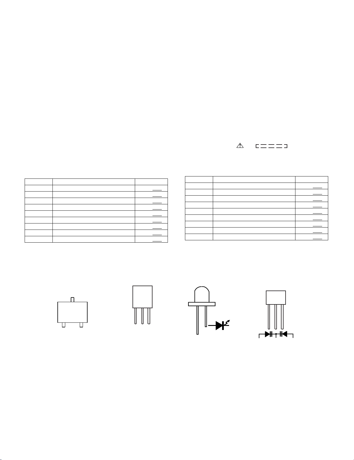
XL-DV60
Home StereoXL-DV60Service ManualXLDV60 Service ManualMarketE
CHAPTER 6. CIRCUIT SCHEMATICS AND PARTS LAYOUT
[1] NOTES ON SCHEMATIC DIAGRAM
•Resistor:
To differentiate the units of resistors, such symbol as K and M are
used: the symbol K means 1000 ohm and the symbol M means
1000 kohm and the resistor without any symbol is ohm-type resistor. Besides, the one with “Fusible” is a fuse type.
• Capacitor:
To indicate the unit of capacitor, a symbol P is used: this symbol P
means micro-micro-farad and the unit of the capacitor without such
a symbol is microfarad. As to electrolytic capacitor, the expression
“capacitance/withstand voltage” is used.
(CH), (TH), (RH), (UJ): Temperature compensation
(ML): Mylar type
(P.P.): Polypropylene type
• Schematic diagram and Wiring Side of P.W.Board for this model
are subject to change for improvement without prior notice.
REF. NO DESCRIPTION POSITION
SW700 VOLUME ON—OFF
SW701 EQUALIZER ON—OFF
SW702 TUNING DOWN/STOP ON—OFF
SW703 TUNING UP/PLAY ON—OFF
SW704 PRESET UP ON—OFF
SW705 PRESET DOWN ON—OFF
SW706 DISC1 ON—OFF
SW707 DISC2 ON—OFF
SW708 MEMORY/SET ON—OFF
• The indicated voltage in each section is the one measured by Digital Multimeter between such a section and the chassis with no signal given.
1. In the tuner section,
( ) indicates AM
< > indicates FM stereo
2. In the main section, a tape is being played back.
3. In the deck section, a tape is being played back.
( ) indicates the record state.
4. In the power section, a tape is being played back.
5. In the CD section, the CD is stopped.
• Parts marked with “ ” ( ) are important for
maintaining the safety of the set. Be sure to replace these parts
with specified ones for maintaining the safety and performance of
the set.
REF. NO DESCRIPTION POSITION
SW709 POWER ON/STAND-BY ON—OFF
SW710 X-BASS/DEMO ON—OFF
SW711 DVD/CD ON—OFF
SW712 TUNER(BAND) ON—OFF
SW713 VIDEO/AUX ON—OFF
SW714 DISC3 ON—OFF
SW715 DISC4 ON—OFF
SW716 DISC5 ON—OFF
SW717 OPEN/CLOSE ON—OFF
[2] TYPES OF TRANSISTOR AND LED
C
(2)
B
(3)
2SC3052F+
2SA1235F+
2SC8050
2N3904
2N2907
2SB1132
2SK3018
BAT54S
(1)
E
FRONT
VIEW
EC B
(S) (G) (D)
(1) (2) (3)
2HC1815 GR
KRA107 M
KRC107 M
2HA1015 GR
2SC535 C
KTC3200 GR
2SB562 C
KTC3203 Y
KTA1271 Y
KTC102 M
KTC3203 Y
KRC104 M
LP3052A+
FRONT
VIEW
123
SVC348S
KDV147B
6 – 1
Page 23
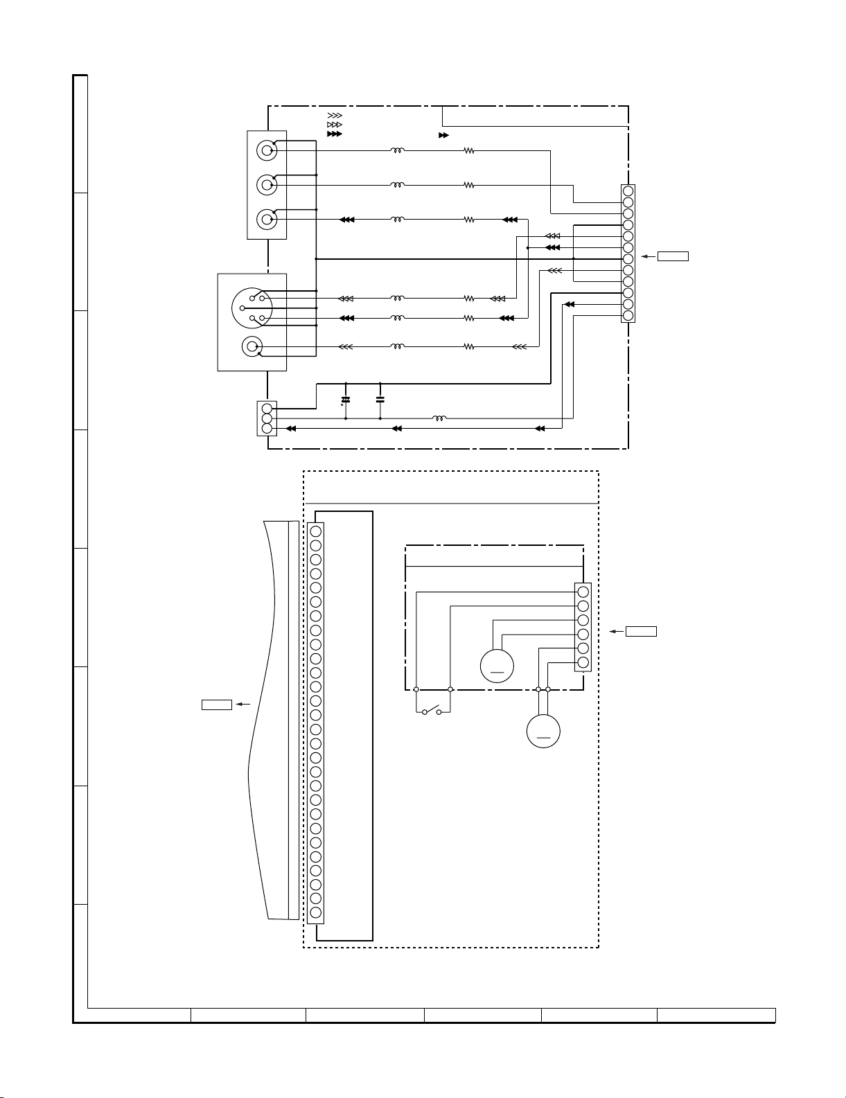
[3] SCHEMATIC DIAGRAM VIDEO TERMINAL
XL-DV60
VIDEO SIGNAL
VIDEO C SIGNAL
A
COMPONENT
VIDEO OUT
S901
Y
P
B
R
P
1
2
R
3
4
B
5
6
G
VIDEO Y SIGNAL
L905
L906
L904
FB
FB
FB
B
S902
S-VIDEO
OUT
VIDEO
OUT
2
4
1
5
3
6
7
L907
FB
FB
L903
FB
VIDEO TERMINAL PWB-B2
DIGITAL(DVD/CD) SIGNAL
R903
R901
R904
75
R906
R905L902
R902
0
0
0
75
0
CNP904A
Cb/Pb
Cr/pr
GNDV
C/V
G/Y
GNDV
CVBS
GNDV
GND
OPTICAL
VCC
1
2
3
4
5
FROM DVD PWB(3/3)
6
CNW3
7
6-14 12-C
8
9
10
11
12
C
C902
1
S903
AUDIO
DIGITAL OUT
2
3
D
E
TO DVD PWB (2/3)
JP1B
6-11 1 - C,D
F
FFC1B
G
10/16
DVD MECHANISM UNIT ASS'Y(220)
1
1
2
3
4
5
6
7
8
9
10
11
12
13
14
15
16
17
18
19
20
21
22
23
24
25
26
27
28
28
PICKUP UNIT ASS'Y
C903
L901
0.1
10µH
+B
DVD MECHANISM PWB
SLED
+
MOTOR
M
SWITCH
SPINDLE
MOTOR
MGND
1
SW
2
SLEG-
3
SLEG+
-
LOAD+
LOAD-
+
-
FROM DVD PWB (2/3)
4
5
6
CNW4
6-11 2-E
M
H
1
23456
Figure 6-2 SCHEMATIC DIAGRAM (1/13)
6 – 2
Page 24
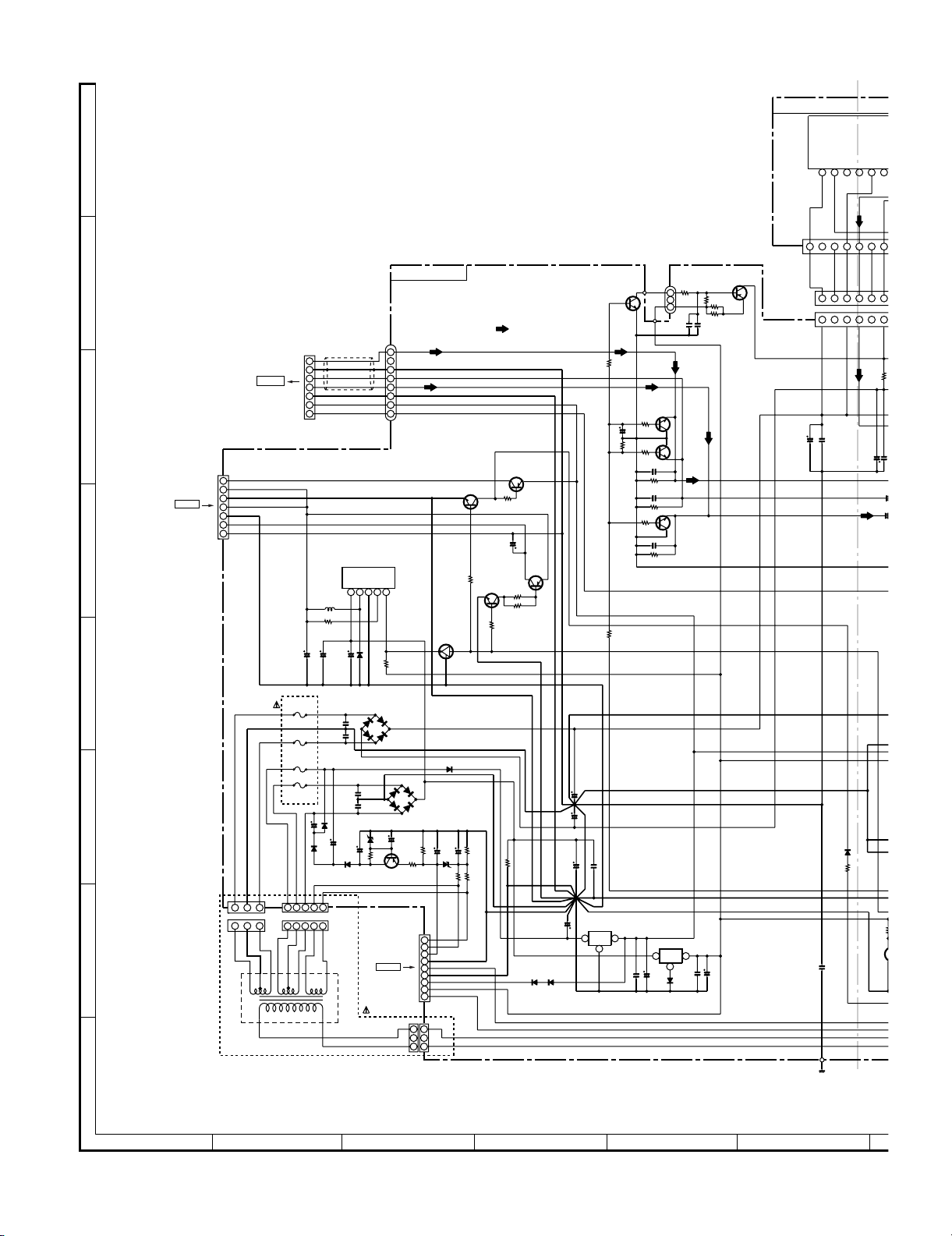
XL-DV60
1
Q107
[4] SCHEMATIC DIAGRAM MAIN/POWER AMP.
POWER AMP. PWB-D
A
CNW205
A GND
+B
R228
C161
470K
1
R223
1.5K
+B
+B
+B
+B
C222
+B
Q208
2SA1235 F+
R221
1.5K
47/25
CNS205
CNP205
-B
+B
C135
10/50
+B
-B
B
MAIN PWB-A1
Q207
2SC3052 F+
FM SIGNAL
L_CH
1
+5V+B
IC203
LM2576T
2345
1
6800/25
D231
C205
C206
ZD201
DZH3001+
C207
R202
22K
2
3
4
5
6
7
8
R245
100K
1N5822
D201
TS6B04 GM
-B
0.1
0.1
Q201
2HA1015 GR
CNS101
6-7 2-C
FROM
DISPLAY PWB
A_GND
R_CH
S/W
GND
+12V
+7V
CNW602
+B
+B
C208
47/50
R204
47K
R203
+B
10
VF2
VF1
3
Q116
KRC107 M
2
D205
KBP304 GM
330/35
C209
-B
R206
3.8V
1
3.8V
2
-30V
3
D_GND
4
+5.6V
5
MGND
6
+10V
7
+5.6V
8
P_CON
9
CNP101
CNP203
22
131
Q118
2HC1815 GR
R246
10K
3
1
D232
1N4004
C210
ZD202
DZH06C2+
330
100/50
DGND
C245
470/16
Q214
2SC3052 F+
R233
10K
+B
DGND
12K
R205
330
R207
+B
+B
Q117
2SB562 C
R247
1.2K
-B1
+B2
+B
R232
1.2K
R234
1.2K
+B
AGND
+B1
10K
R241
D112
1N4004
Q213
+B
2SB562 C
1N4004
D111
C237
+B
+B
-B
C214
2200/35
+B
10K
R219
+B
+B
+B
C211
4700/35
C212
4700/35
0.047
C215
6800/25
IC202
KIA7812API
2
C134
33/16
6.8K
R154
C171
220P
R155
3.3K
REGULATOR
31
1
2
6-6 9-A
3
4
5
6
7
CNS602
+B
+B
VOLTAGE REGULATOR
L206
100µH
+B
R224
120
C216
220/16
C217
470/16
C236
CNP602
TO TUNER PWB
C
S12V
1
VCC1
2
GND
3
4
5
6
7
CNP807
VCC2
GNDRF
VCCA
GNDA
CNW2
FROM DVD PWB (3/3)
6-13 2-E
D
E
F201
6.3A 125V
C203
0.1
F202
C204
6.3A 125V
0.1
F204
3.15A 125V
F203
2A 125V
F
CNP202
321
321
C225
D209
100/50
1N4004
54321
54321
D210
1N4004
220/50
C226
100/50
D211
1N4004
CNP204
G
T201
POWER TRANSFORMER
(MAIN)
+B
Q101
2HC1815 GR
R104
10K
R105
10K
220P
C101
R107
1K
C102
220P
1K
R108
R175
10K
1K
R172
VOLTAGE
+B
IC201
KIA7805API
C219
0.022
D212
1N4004
C220
220/25
R220
CNW207
3
2
1
C160
1
Q102
Q115
2
1K
2HC1815 GR
2HC1815 GR
C221
0.047
31
VEE
VCC
123456
37465
1
VCC
C137
0.1
D202
1N4148
R201
12K
C213
0.047
CHASSIS GND
VCC
NC
VCC
NC
NC
422 53 61
42 53 61
L_OUT
MUTE1
4.7K
R119
C136
10/50
C
1/
C1
10/
+B
+B
Q203
KTC3200 GR
+B
H
1
23456
Figure 6-3 SCHEMATIC DIAGRAM (2/13)
6 – 3
Page 25
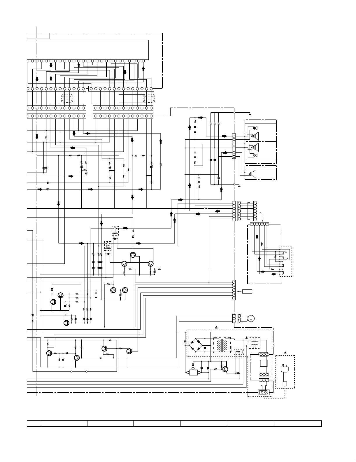
XL-DV60
VEE
P. PWB-D
VEE
L_OUT
NC
VCC
NC
NC
23456789
+B
5
573
C136
R119
10/50
+B
Q203
6
MUTE1
4.7K
C105
1/50
C106
10/50
+B
KTC3200 GR
C138
0.1
Q107
9
73
L_IN
R_OUT
D108
1N4148
Q108
2SC3052 F+
2SC3052 F+
Q109
2HC1015 GR
22K
R209
R210
3.3K
R211
374685
42
42
VCC
L_OUT
137
.1
202
4148
201
2K
13
47
HASSIS GND
IC101
LM4781TA
POWER AMP.
S/W_OUT
NC
R_RF
MUTE2
GND
NC
VEE
R_IN
R_OUT
L_RF
L_IN
MUTE1
GND
NC
10 11 12 13 14 15 16 17 18 19 20 21 22 23 24 25 26
10
98
10
98116
VEE
GND
L
C139
47/50
R157
D213
1N4004
C223
47/1610K
18K
11
R_RF
R122
18K
R212
S/W_OUT
R137
R139
R138
R156
5.6K
22K
141110
1312
1312
MUTE3
R113
1K
R149
470
C107
47/50
D107
1N4004
+B
2SC535 C
CFW201
56K
56K
56K
Q202
1512 13
14
14
S/W_IN
R141
D105
1N4148
R213
470K
VCC
21
2345 7 9
1
2345 7 9
1
VEE
R110
1K
R116
39K
C104
1/50
R
6.8
6.8
R134
R135
C120
0.022
0.022
C119
0.022
C122
C123
C140
0.0022
R140
R142
100K
100K
100K
D104
1N4148
D106
1N4148
Q204
2HA1015 GR
C224
10/16
R136
0.022
R150
47/50
R117
39K
RLY101
1
6.8
C121
0.022
C124
0.022
R158
10K
Q110
KRA107 M
R216
VEE
470
C108
65
D109
27K
R214
-B
RLY102
432
1N4004
+B
30
8
68
68
VCC
GND
L_RF
+B
R114
1K
R123
18K
21
43
D110
1N4004
Q112
2HC1815 GR
R159
47K
Q111
KRC107 M
1
3
23
C141
3.3/16
R215
3.3K
9547
R_IN
R111
L
R
R161
1
GND
106311
1K
+B
4.7K
2
Q205
2HC1815 GR
S/W_RF
MUTE3
12
1110 13
1110 13
MUTE2
R115
R124
33K
1K
R160
220
ZD101
DZH06B2+
Q113
2HC1815 GR
S/W_IN
27
CNW206
14
13
12
12
GND
S/W_RF
R151
470
C109
3.3/50
R118
39K
R163
47K
+B
+B
CONSTANT
VOLTAGE
REGULATOR
CNS206
CNP206
R112
1K
Q114
2HC1815 GR
R162
4.7K
C142
47/16
IC204
AN78L05
C227
2200/16
+B
D216
1N4004x4
D215
D218
1N4004
CHASSIS GND
R143
0.0047
0.0047
C165
C132
0.0047
0.1
0.1
4.7
R145
SUB_RELAY OUT
POWER TRANSFORMER
C228
0.047
C230
47/25
R217
+B
0.0047
C167
C169
0.0047
C131
C133
0.0047
RIN
ROUT
A_GND
L OUT
SUB_RELAY IN
CNP103A
SP_RELAY
SINGAL_LVL
FAN_START
SP_DETECT
P_MUTE
FAN_PRO
CD+B
CNP102
CNP208
T202
(SUB)
R218
47K
10K
LIN
4.7
C125
0.1
C128
0.1
C126
0.1
C129
0.1
R144
4.7
C130
C127
L105
2.2µH
D217
D214
C229
0.047
2
31
+
L-CH
-
+
R-CH
-
+
-
SO101
SPEAKER TERMINAL
1
1
2
2
3
3
4
4
5
5
6
6
7
7
CNW103
1
2
3
4
5
6
FROM DISPLAY PWB
7
CNW208
3
3
22
1
1
Q206
2HC1815 GR
D219
1N4004
SPEAKER BOX ASS'Y
TWEETER
+
6ohm
WOOFER
-
+
6ohm
WOOFER
TWEETER
SPEAKER BOX ASS'Y
SUB WOOFER BOX ASS'Y
+
6ohm
-
CHASSIS
GND
MR101
CORE
1
2
3
4
5
6
7
LIN
L OUT
A_GND
SUB_RLY IN
L103
SUB_RLY OUT
JACK PWB-B3
CNS102
6-7 2 - F
M201(218-4)
M
FAN MOTOR
LF201
LINE FILTER
CNW201
31
RLY201
RELAY
MR201
CORE
CNS201
3
31
CNP201
SO202
AC
SOCKET
R OUT
10µH
R147
2
21
2
1234567
220
RIN
R146
L-CH
R-CH
CNP103B
220
JK101
HEADPHONES
1
3
11
10
2
9
8
7
6
5
4
AC POWER
SUPPLY CODE
AC 120V 60Hz
7
8 9 10 11 12
Figure 6-4 SCHEMATIC DIAGRAM (3/13)
6 – 4
Page 26
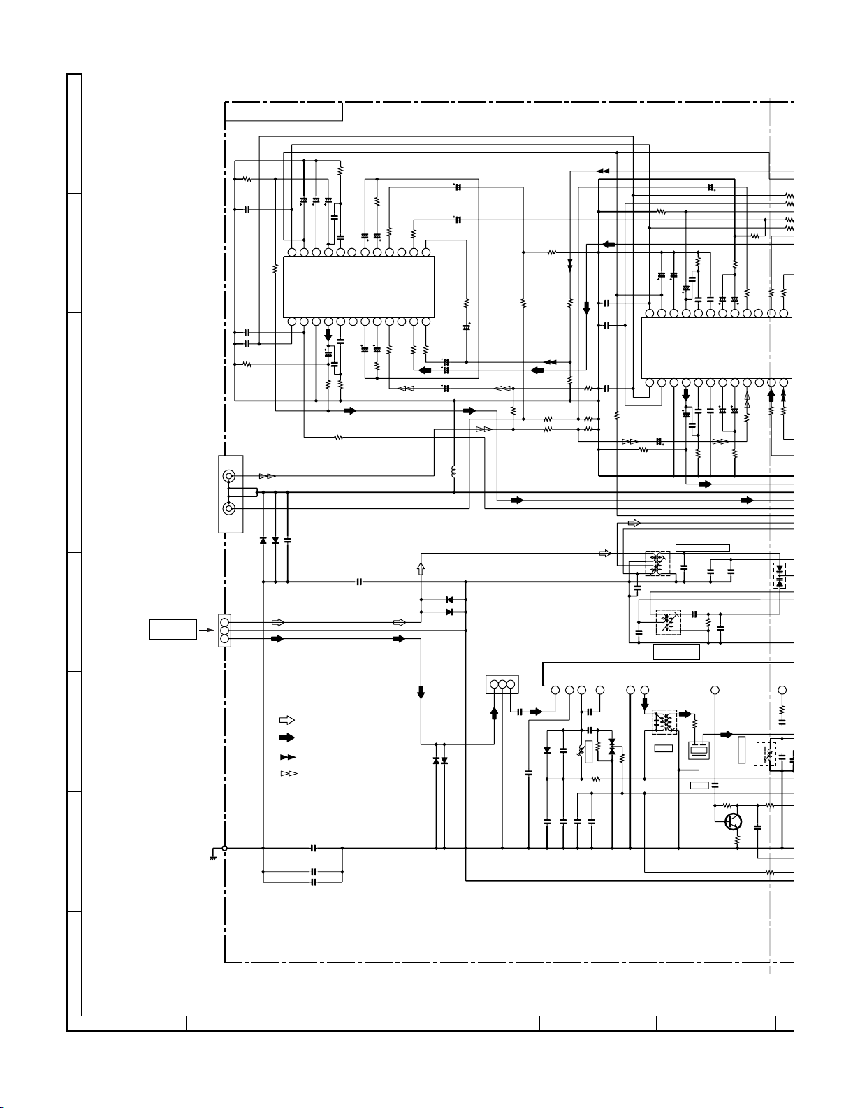
XL-DV60
6
10/16
K
K
+
6
6
[5] SCHEMATIC DIAGRAM TUNER
TUNER PWB-A2
A
B
C
L-CH
SO601
D
E
VIDEO/AUX
AUDIO IN
AM LOOP/FM
ANTENNA
R-CH
1
2
3
CNP301
AM
GND
FM
F
G
CHASSIS
GND
R683
100K
C681
220P
C682
220P
C683
220P
R675
100K
+B
33/16
100/16
C669
C671
1K
R696
CL
VDD
DI
CE
123456789
C678
D604
1N4148
D605
1N4148
C634
0.0027
AM SIGNAL
FM SIGNAL
DVD/CD AUDIO SIGNAL
AUX SIGNAL
C388
0.1
C349
0.001
C301
0.012
VREF
VSS
R691
AUX_R
3.9K
R694
10/16
C696
0.1(ML)
C695
C693
10/16
C694
0.1(ML)
RIN
RBS
RTRE
ROUT
SIGNAL CONTROL
LIN
LTRE
LOUT
LBS
C674
0.1(ML)
10/16
C670
10/16
C676
0.1(ML)
3.9K
R676
1K
R648
CE WOOF
1K
AUX_L
A_GND
C302
0.001
10K
R692
1K
R685
C667
10/16
R4R3R1
RSL0
IC603
LC75341M
LSL0
L4
10 11 12
C668
10/16
1K
R686
10K
R677
R678
DI
CL
+7V
C663
10/16
1K
C662
10/16
A_GND
1N4148
10/16
AUX R
AUX R
TUN R
DVD/CD SUB
TUN L
AUX L
BAND PASS
FILTER
BF301
22K
R640
R641
22K
R645
R665
FM FRONT END
321
C319
18P
(CH)
0.01
C304
R642
5.6K
R631
1.2K
22K
22K
IC301
TA7358AP
0.8V
1133456 7 82
1N4148
D306
0.0047
0.0047
C305
C307
C661
1K
R679
131415161718192021222324
R2
R617
L1L3L2
C604
10/16
R680
1K
1K
C666
10/16
C664
10/16
AUX L
L601
2.2µH
D301
1N4148
D302
1N4148
D305
D307
1N4148
R634
1.5V
9P
C306
1.8K
(UJ)
0.022
C308
R646
5.6K
R643
2.2K
R644
2.2K
5.2V
C303
0.001
L302
FM RF
R301
0.001
C309
+B
C625
1/16
DI
CE
R622
100K
CL
3.9K
R613
C617
33/16
C618
100/16
0.1
C623
C621
220P
C619
220P
+B
24 23 22 21 20 19 18 17 16 15 14 13
CL
VDD
C616
47/16
VREF
ROUT
C614
C612
0.1(ML)
RBS
0.0027
RTRE
SIGNAL CONTROL
LBS
LTRE
LOUT
C624
1/16
100K
AM ANT
T302
C329
0.022
AM OSC
T306
AM BAND
COVERAGE fL
5.2V
T304
FM IF
VSSDICE
0.1
C622
C611
0.0027
C615
C613
47/16
0.1(ML)
3.9K
R612
AM TRACKING fL
C330
C331
12P(CH)
C335
560P
68K
R323
4.4V
47
R307
2
CF303
FM IF
Q302
2SC535 C
C620
220P
120
R630
R623
+B
0.022
C337
0V
1.5V
C318
5P
VD303
KDV147B
100K
R302
33K
R303
22
R666
C610
C608
10/16
10/16
RIN
RSL0
LC75341M
LSL0
LIN
C607
10/16
C609
10/16
22K
R667
0.047
0.022
C332
(UJ)
C334
27P
C311
10P (CH)
R304
47K
AUX R
R609
47K
22K
IC601
L4
R628
AUX L
FM OSC.
33
R315
R310
+B
R603
R602
R608
R601
1K
R629
R607
R4R3R2
1K
R606
VD301
R306
C312
33P
L303
R305
680
100P
C315
1K
R
L1
L2R1L3
121110987654321
R
1K
SVC348S
3.8V
33
4.7K
1
1
C313
C316
P
H
1
23456
Figure 6-5 SCHEMATIC DIAGRAM (4/13)
6 – 5
Page 27
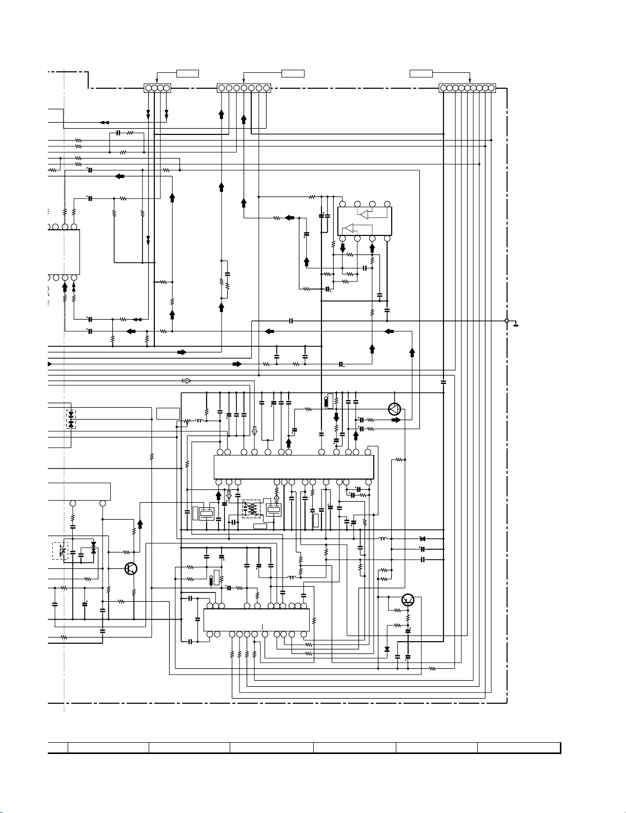
XL-DV60
33
R4
L4
629
L303
+B
XR
R603
R602
R608
R601
R609
47K
1K
1K
R
R607
R605
15 14 13
R3
R2
C601
5341M
NTROL
L1
L2R1L3
121110
R604
1K
1K
R606
XL
VD301
SVC348S
3.8V
89
R306
33
C312
33P
R305
680
100P
C315
4.7K
R310
1K
1K
C313
C316
12K
1K
+B
6P
10/16
1K
1K
(UJ)
R308
10K
C314
22P
C602
1/16
C601
1/16
C606
1/16
C605
1/16
C317
C638
CE WOOF
5.2V
+B
VD302
KDV147B
(CH)
0.022
0.47/50
R621
R620
4.7K
2SC535 C
R313
R309
C321
0.0033
4.7K
R624
47K
Q306
680
470
R312
2.2K
CNP904
R684
680
R636
1K
CD R
R625
47K
R618
330
R316
33
R314
CD L
5.6K
DVD/CD_L
5.6K
R619
5.6K
R336
D_GND
S/W_CH
C361
0.022
2.1V
(2.7V)
FM AFC
0.022
C350
T351
0.001
0.9V
AIN
4.8V
R372
2.1V
AM RF
AM IF
0.9V
DO
5.1V
1K1K1K
R371
+12V
+B
R615
3.9K
+B
(2.7V)
IN
C380
PD
C363
10/16
R379
7654321
+7V
0.022
2021222324
2.2K
1.7V
0.6V
FROM MAIN PWB
CNS602
+B
R661
10
0.047
47/25
R658
1K
R688
C633
0.0027
R681
C697
3.9K
0.47/50
A_12V
C364
10/16
0.001
C366
C365
0.022
C367
0V
(0.9V)
2.3V
CUT
OUT
VSM
FM/AM
AM LOW
SD
GND
AM IF
IN
4
56 78 9 1011 12
5V
0V
5V
1K
R352
3
1
C353
0.022
C354
2
CF352
C387
0.022
L351
100µH
(0V)
2.6V
0.01
5.2V
C385
0V
(2.6V)
12131516171819202122
14
VDD
FM IN
AM IN
FMFMMUTE
MO/ST
8910 11
R359
3.5V
(0V)
(0V)
3.9V
3.7V
1.8K
(11.4V)
R360
4.7K
22/16
C652
22K
R350
2.7K
1/50
STEREO
5V
0.022
R393
1K
R377
5.6K
IF REQ
C698
CF351
C386
0V
IF IN
0.47/50
X351
FM DET
R353
330P
C639
R663
22K
C640
100/16
456KHz
171819
2.3V
MPX VCO
2.9V
(4.3V)
270
C399
FM IF
47K
R395
+B
10K
R365
R662
(0V)
VCC
0.022
C657
22K
TP302
R356
C368
2.1V
5V
C398
+B
R357
1K
1/50
MPX IN
0V
100/10
TUN_R
IC602
NJM4558D
BUFFER AMP.
+
+
-
2
134
R687
R659
22K
5.6K
R655
C635
0.27/63
10K
(ML)
R651
8.2K
470K
C369
IF OUT
C355
TUN_L
C656
10/16
C374
56P
1.3V
R-CH
3.8V
(1.9V)
C357
2.2/50
C356
22P
0.022
14151613
OUT
PHASE
C358
1/50
0.001
R387
1.3V
C371
L-CH
5.6K
1/50
C372
1/50
OUT
C370
R649
C373
0.022
MO/ST
1/50
5.6K
(AM/FM)
PHASE
3.3K
R355
R376
0.022
C383
R361
0
R362
0
4V
3.8V
(1.2V)
10K
L352
100µH
D308
C631
4.7V
(0V)
(2.2V)
R391
390
+B
1N4148
FROM DVD PWB (3/3)
CNW1
6-14 12-B 6-3 2-C 6-7 2-D
4321
A_GND
DVD/CD_R
R610
12K
CD_A_GND
R616
47K
R611
12K
FM MUTE
LEVEL
VR351
+B
DVD S/W_CH
TUN R
R614
12K
TUN L
L353
5.6K
R351
C351
0.022
R382
330
R386
330
C381
12P
(CH)
X352
C382
15P
(CH)
PLL(TUNER)
CNP602
R358
8.2K
1mH
2.1V
CF302
1
3
FM IF
C344
2
33P
C397
0.022
VT
2.6V
XIN
4.5MHz
2.6V
IC302
LC72131
L_CH
R_CH
A_GND
C637
0.47/50
1K
680
R682
R635
33P
C343
C360
0.022
3.3/50
C362
5V
2.5V
IN
OUT
AM OSC
AM OSC
REG
IN
FM IF
AM MIX
OUT
132
2.1V
2.1V
C352
10/16
C378
330P
C394
47/16
C392
10K
R381
TP301
R380
C393
1.5K
1/50
VSS
XOUT
AOUT
CEDICL
3421567
0V
0.1V
0.1V
1K
R374
R373
FROM DISPLAY PWB
CNS302
5678
0.27/63(ML)
C632
0.0027
Q351
KRC104 M
TUN_L
R366
2.2K
DZH05C2+
+B
+B
R392
390
Q360
2HA1015 GR
10.8V
11.7V
R383
5.6K
10.9V
R385
5.6K
R384
6.8K
C202
0.022
CNP302
C384
0.001
TUN_R
IC303
LA1832S
FM IF DET./FM MPX./AM IF
ZD351
C396
100/10
C395
0.022
+B
FM ST
C391
47/16
C201
100/16
R399
987654321
DI
CL
CE
SD
DO
FM ST
D_GND
CE WOOF
CHASSIS
GND
D_GND
SD
A_12V
+B
10
DO
CL
DI
CE
7
8 9 10 11 12
Figure 6-6 SCHEMATIC DIAGRAM (5/13)
6 – 6
Page 28
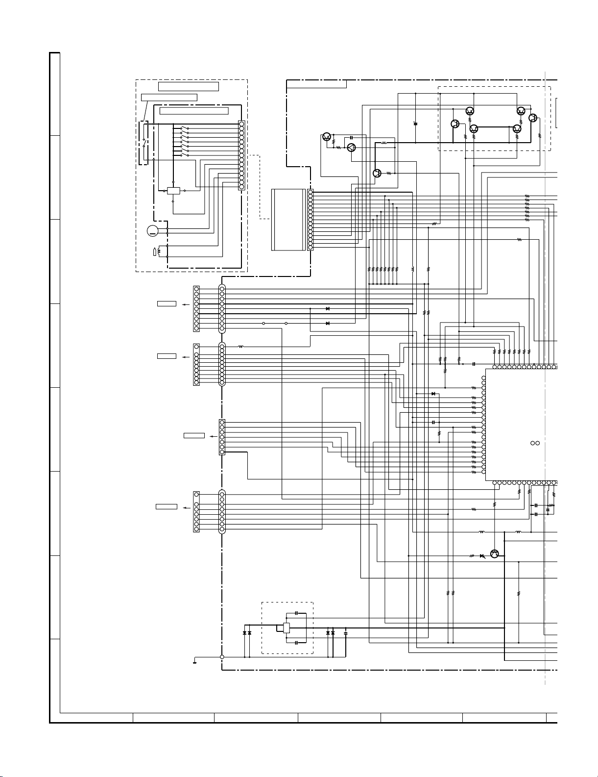
XL-DV60
K
6
VSS1
M
R
L702
7
[6] SCHEMATIC DIAGRAM DISPLAY
R510
390
R773
R735
10K
+B
270
470
R750
R755
R702
R730
R701
R706
R746
R747
R748
R749
R728
R729
R731
C702
R719
R703
Q505
KTA1271 Y
2HC1815 GR
22K
R511
MM-
MM+
0.1
81
82
1K
83
84
1K
85
1K
86
1K
87
1K
88
89
90
1K
91
1K
92
93
1K
94
1K
95
1K
96
1K
97
1K
98
1K
99
1K
100
R733
1K
L704
0.82µH
LED701
LP3052A+
2HC1815 GR
MOTOR DRIVER
Q506
2.7K
Q507
2HC1815 GR
R504A
R503A
R505A
R506A
R502A
R501A
R507A
R508A
220
1K1K1K
1K
R712
R720
R721
R722
R723
SD
SPAN
FM_ST
P_STB
JOG_UP
CD+B
NC
JOG_DOWN
CE
DI
CL
SP_RELAY
VSS2
VDD2
DO
SP_DETECT
NC
SINGAL_LVL
DVD_DI
DVD_DO
DVD_CLK
DVD_BUSY
CLID_OUT
CE WOOF
NCNCNCNCNC
123456789
R707
L708
0.82µH
Q705
Q508
KTA1271 Y
R513
R512
22K
1K
220
220
R725
R724
MM-
MM+
CD_SOL
FAN_START
P_CON
R727
470
R514
1K
1K
1K
1K
1K
1K
1K
1K
R758
VDD4
CD_PH
TIMER_LED
12
P_MUTE
R705
1K1K
C703
24P
(CH)
C704
24P
(CH)
10K
390
SUB WOOF SEL
SW8
11 12 1310
KTC3203 Y
Q509
SW7
RESET
R741
X701
68697071727374757677787980
SW6
SW5
XT1
XT2
R
1
1
10M
32.768kHz
15 15
FC501
CFW750
SW700
VOLUME
JOG
D
E
DISPLAY PWB-B1
Q503
2SB562 C
+9V
R525
270
(1W)
11
D_GND
1
SW4
2
SW3
3
SW5
4
SW6
5
SW2
6
SW1
7
SW7
8
CD_PH2
9
CD_PH3
10
MM+
11
CD_SOL1
12
MM-
13
CD_SOL2
14
SW8
15
CNP501
1N4004
D701
1N4004
D708
+B
+B
+B
C714
0.001
A
B
C
C715
0.001
D710
1N4148
R526
56K
D709
1N4148
C515
0.022
Q502
KRC102 M
+B
C720
0.1
+B
C506
L503
0.82µH
CD_M_GND
Q511
KTC3203 Y
R521
390
10K
10K
10K
10K
R502B
R507B
R501B
R508B
10K
10K
R503B
R504B
10K
10K
R506B
R505B
47/16
+B
L502
+B
0.82µH
+B
+B
+B
+B
10K
R789
+B
+B
R787
10K
R738
10K
C701
0.1
10K
R788
R737
100
10K
+B
D706
1N4004
R797
10K
Q504
R509
KTC3203 Y
5-DISC_M_GND
R516
R739
10K
R756
10K
+B
10K
R716
5-DISC CHANGER
A
B
C
D
E
F
SWITCH PWB ASS'Y(133)
CD CHANGER PWB ASS'Y(132)
PHOTO
INTERRUPTER
M
MOTOR
(125)
SOLENOID
(124)
CNP101
6-3 3-G
TO MAIN PWB
CNP302
6-6 11-A
TO TUNER PWB
6-9 1-B
TO DVD PWB (1/3)
CNP102
6-4 11-F
TO MAIN PWB
CNW5
1
2
3
4
5
6
7
8
9
1
2
3
4
5
6
7
8
9
1
2
3
4
5
6
7
CNS101
CNS302
D_GND
SW4
SW3
SW5
SW6
SW2
SW1
SW7
CD_PH2
CD_PH3
MM+
CD_SOL1
MM-
CD_SOL2
SW8
3.8V
1
3.8V
2
-30V
3
D_GND
4
+5.6V
5
M_GND
6
+10V
7
+5.6V(MOTOR)
8
P_CON
9
CNW101
D_GND
1
2
SUB_WOOF_SEL
3
CE_WOOF
4
SD
5
FM_ST
6
DO
7
CL
8
CE
9
DI
10
CNW302
DVD_STB
1
CLID_OUT
2
DVD_BUSY
3
DVD_CLK
4
DVD_DI
5
DVD_DO
6
D_GND
7
CNP802
SP_RELAY
1
2
SINGAL_LVL
3
FAN_START
4
SP_DETECT
5
P_MUTE
6
FAN_PRO
7
CD+B
8
CNW102CNS102
1
2
3
4
5
6
7
8
9
10
11
12
13
14
15
F2
F1
L707
0.82µH
G
D712
1N4148
D713
1N4148
CFW751
CHASSIS
GND
H
1
23456
Figure 6-7 SCHEMATIC DIAGRAM (6/13)
6 – 7
Page 29
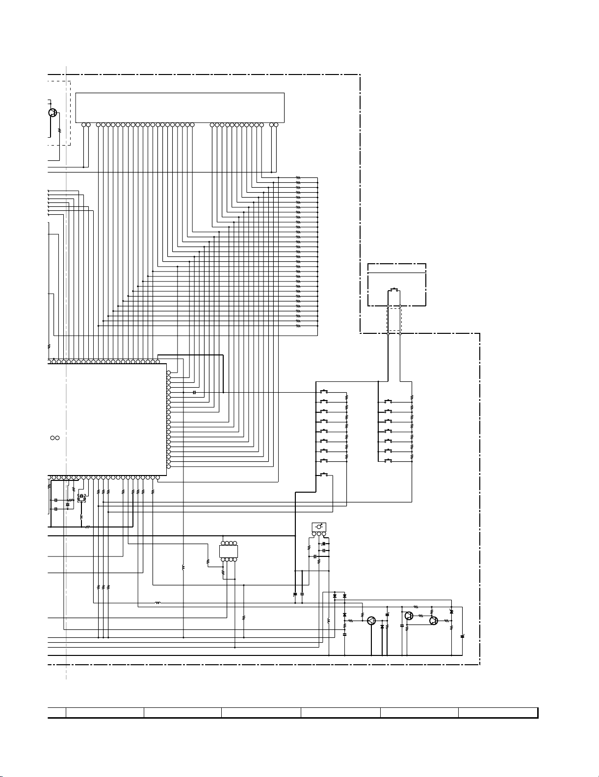
XL-DV60
1K
470
P
MUTE
CD
PH
R758
1271 Y
P11
P12
P15
P14
P17
P18
P16
P20
P19
F2F2NP
KTC3203 Y
Q509
390
R514
1K
1K
1K
1K
1K
1K
1K
360
_
SW8
SW7
VDD4
TIMER_LED
12
_
NC
89
R705
1K
C703
24P
(CH)
C704
24P
(CH)
SUB WOOF SEL
NC
RESET
11 12 13 14 15 16 17 18 1910
XT1
R741
X701
P20
SW4
SW3
SW2
SW1
SW6
SW5
IC701
IXA009SJ
SYSTEM
MICROCOMPUTER
XT2
VSS1
CF1
CF2
VDD1
KEY1
KEY2
R740
1K
1K
1K
3
1
10M
32.768kHz
2
L702
R745B
X702
0.82µH
0
8MHz
+B
R708
10K
R742
R709
10K
R743
616263646566676869707172
P17
P18
P16
P19
RDS_DATA
RDS_VSM
POWER_KEY
21 22 23 24 25 26 27 28 29 3020
1K
R710
10K
R744
P15
P14
FAN_PRO
PATCH
1K
1K
R714
R713
P13
P12
P13
DVD_STB
MODEL
SYS_STOP
1K
1K
R715
R732
P11
L701
P9
P10
515253545556575859
P9
VP
P10
P8
P7
P6
P5
VDD3
P4
P3
P2
P1
NC
11G
10G
9G
8G
7G
6G
5G
4G
3G
2G
RDS_CLE
1G
IRQ
R718
0.82µH
P7P6P8
1K
VFD701
P5P4P1
50
49
48
47
46
45
44
43
42
41
40
39
38
37
36
35
34
33
32
31
L703
0.82µH
5G
456789
IC702
AT24C04
EEPROM
R704
10K
NPF1F1
12
R752A
R752B
R752C
R752D
R752E
R752F
R752G
R752H
R752I
R752J
R752K
R753A
R753B
R753C
R753D
R753E
R753F
R753G
R753H
R753I
R753J
R753K
R753L
R753M
R753N
R753O
R753P
R753Q
R753R
R753S
R753T
C706
220/10
82K
82K
82K
82K
82K
82K
82K
82K
82K
82K
82K
82K
82K
82K
82K
82K
82K
82K
82K
82K
82K
82K
82K
82K
82K
82K
82K
82K
82K
82K
82K
SW708
SW707
SW706
SW705
SW704
SW703
SW702
SW701
SW709
R751
1K
C708
100P
C707
0.1
MEMORY/SET
DISC2
DISC1
PRE SET DOWN
PRE SET UP
TUNING UP/PLAY
TUNING DOWN/STOP
EQ
POWER
ON/STAND-BY
RX701
GP1UD261
REMOTE
SENSOR
321
C709
100/10
C710
0.047
47
R760
D702
1N4148
+B
L705
0.82µH
+B
+B
+B
R761
1K
R772
5.6K
R770
3.9K
R769
2.7K
R768
2K
R767
1.5K
R766
1.2K
R765
1.2K
D703
1N4148
D704
1N4148
R762
1K
C711
0.1
SWITCH PWB-B4
SW717
OPEN/CLOSE
12
12
DISC5
SW716
DISC4
SW715
DISC3
SW714
VIDEO/AUX
SW713
TUNER(BAND)
SW712
SW711
CD/DVD
X-BASS/DEMO
SW710
R763
C712
3.3K
33/16
R764
100K
C713
0.01
D705
1N4148
Q702
KRC102 M
CFW701
R776
R775
R786
5.6K
R785
3.9K
R784
2.7K
R783
2.2K
R782
1.5K
R781
1.2K
R780
1.2K
1K
Q703
2HC1815 GR
R777
10K
2HC1815 GR
82
Q704
R778
10K
R779
120
ZD701
DZH03C3+
1K
R799
C716
47/16
P2
+B
C705
+B
10G
11G
18192021222324252627282930313233343536373940
0.1
R757
1011121314
1234
A2A1A0
GND
VCCWPSCL
SDA
8
6
5
7
1K
10K
R771
6G2G3G
7G1G4G
9G
8G
NPNPNP
P3
7
8 9 10 11 12
Figure 6-8 SCHEMATIC DIAGRAM (7/13)
6 – 8
Page 30

XL-DV60
DB1
DB1
32
S
125
F
+
D
D
C
C
[7] SCHEMATIC DIAGRAM DVD1/3
A
B
C
D
E
F
G
H
DVD PWB-C (1/3)
TO
DISPLAY PWB
6-7 1-E
CNP802
1
2
3
4
5
6
7
CNW5
VCC-DSP3 3
J5
1
1
2
2
3
3
4
4
5
5
6
6
7
7
GND
VCC33
R13 7
R13 9
STB
R23
CLI D
R30
BUSY
R31
CLK
R32
DI
R33
DO
R34
GND
ST B0 CL I D0 BUS Y0 CLK0 DI 0 DO0
22P 22P 22P 22P
(CH)
(CH) (CH)
GND
U1 0
24C02
SERIAL EEPROM
1
S0
VCC
2
S1
WC
3
S2
SCL
4
GND
SDA
MA0
MA1
MA2
MA3
MA4
MA5
MA6
MA7
MA8
MA9
MA10
MA11
DSCK
R15
DO E#
R16
CS0#
R17
RAS0#
R18
CAS#
R19
DW E #
R20
DQ M
R21
RAS1#
R22
RAS2#
R24
L32
FB
VCC- DRAM
+
C11 7
1 0/16
GND
RXD
4.7K
TXD
4.7K
STB0
33
CLI D0
33
BUSY0
33
CLK0
33
DI 0
33
DO0
33
C18 1C18 2 C18 3 C1 8 4 C18 5 C18 6
22P22P
(CH) (CH)
TP31
TRACK
TP19
FOCUS
SPINDLE
FOCUS
SLEGN
TRACK
SVREF15
SCSJ
SDATA
SCLK
VCC
8
7
6
5
GND
33
33
33
33
33
33
33
33
33
C61 C6 2 C6 3 C6 4 C6 5 C66 C67
0.1 0.1 0.1 0.1 0.1 0.1 0.1
TP20
SLEGN
TP26
SPINDLE
SPI NDL E
FO CUS
SLEG N
TRACK
SVREF1 5
SCSJ
SDATA
SCLK
1K
3664164T
64M SD-RAM
23
A0
24
A1
25
A2
26
A3
29
A4
30
A5
31
A6
32
A7
33
A8
34
A9
22
A10
35
A11
38
CLK
37
CKE
19
CS
18
RAS
17
CAS
16
WE
15
DQML
39
DQMH
20
BA0
21
BA1
36
NC
40
NC
C17 3
0.015
U1 3
(CH)
PLLGND
(CH)
C16 6
C16 5
33P
R70R71
1K
RFGND
R27
R28
DQ0
DQ1
DQ2
DQ3
DQ4
DQ5
DQ6
DQ7
DQ8
DQ9
DQ10
DQ11
DQ12
DQ13
DQ14
DQ15
VCC
VCC
VCC
VCCQ
VCCQ
VCCQ
VCCQ
VSS Q
VSS Q
VSS Q
VSS Q
VSS
VSS
VSS
0.1
C51
560P
C17 2
C17 8
0.015
(CH)
33P
VCC-DSP3 3
33
33
VCC
2
4
5
7
8
10
11
13
42
44
45
47
48
50
51
53
1
14
27
3
9
43
49
6
12
46
52
28
41
54
GND
NOTES ON SCHEMATIC DIAGRAM can be found on page 6-1
PLLGND
C18 0
(CH)
C16 4
DB0
DB1
DB2
DB3
DB4
DB5
DB6
DB7
DB8
DB9
DB10
DB11
DB12
DB13
DB14
DB15
TP27
MIRR
TP23
DIP
TP17
DIN
R15 1
4 7P (CH)
C17 6
560P
HOMES W
CD-DVD-CTR
33P
RFGND
RF3 3V
R82
0
RFGND
C53
1.2K
R12 5
R17 4
0.1
MOCTL
C17 1
0.015
R14 1
R14 2
R14 3
R14 4
R99
R10 0
R10 1
R10 2
R10 3
R10 4
NC
GND
NC
RES
VDD
U1 2
V6 3 0 0
RESET
R16 6
R16 7
R17 5
R16 5
R16 8
R29
R26
R25
SDEFCT
SPDON
XOUT
SBAD
MIRR
C57
0.1
C15 4
0.047
C17 7
560P
LDON
SPDON
TP14
1
2
3
4
5
TP15
TP33
TP25
SBAD
TEI
SBAD
FEI
FEI
CEI
CEI
TEI
TEI
MIRR
DI P
DIP
DI N
DIN
C52
C54
0.1
PLL33V
C55
0.1
10K
5.1K
C49
0.1
OPEN
6.8K
6.8K
5.1K
6.8K
6.8K
XSCSJ
33
XSDATA
33
XSCLK
33
SDEFCT
LDON
SPDO N
EAUX01
EAUX02
EAUX00
4.7K
EAUX03
4.7K
EAUX02
4.7K
EAUX01
4.7K
EAUX00
OPE N
STB0
100K
CLI D0
100K
BUSY0
100K
CLK0
100K
DI 0
100K
DO0
100K
VCC
GND
27M
C17 5
27P
(CH) (CH)
GND GNDGND
0.1
RESET#
R98
100K
G1
TP18
FEI
C17 4
27P
TP16
CEI
R17 6
C16 7
0.0068
157
158
159
160
161
162
163
164
165
166
167
168
169
170
171
172
173
174
175
176
177
178
179
180
181
182
183
184
185
186
187
188
189
190
191
192
193
194
195
196
197
198
199
200
201
202
203
204
205
206
207
208
C14 0
0.001
0.001
RFGND
C16 1
0.0047
C16 0
0.0047
68K
R17 8
20K
AVSS_ DS
AVSS_ PL
XSP DOFT R1
XSF DO
XSF TR OP I
AVDD3 _ P L
XSPLLFTR1
XSPLLFTR2
XSVREF 0
XSAWR C
AVSS_ DA
XSRFRPCTR
XST RAY
AVDD3 _ DA
XSS P INDLE
XSF OCUS
XSS LE GP
XSS LE GN
XST RACK
XST ES TDA
XSF GIN
XSP HOI
SXCSJ
XSDATA
XSCLK
XSDFC T
XSL DC
XSS P DON
VD33
VS3 3
XGPIO[9]
XGPIO[8]
XGPIO[7]
XGPIO[6]
XGPIO[5]
XGPIO[4]
EAUX0 3
EAUX0 2
EAUX0 1
EAUX0 0
VSS
VDD
AUX0
AUX1
AUX2/ HS YNC
AUX3/ VS YNC
AUX4
AUX5
AUX6
AUX7
RESET
VS3 3
L35
3.3µH
C13 9
0.001
R90
R87
R88
R89
OPEN
C13 7
C13 8
0.001
C13 6
0.001
3.3K
3.3K
3.3K
3.3K
C50
0.1
155
156
XSDSSLV
VD331XIN2XOUT3DCLK4DMA05DMA16DMA27DMA38VS339VD3310DMA411DMA512DMA613DMA714DMA815DMA916DMA1017VS3318VD3319DMA1120DCAS21DCS022DCS123DRAS0
XI N
+
C16 9
SVREF09
SVREF15
SVREF21
148
149
150
151
152
153
154
XSIPIN
XSRFI P
XSRFI N
XSIREF
AVDD3_DS
XSVREF[21]
XSVREF[09]
XSVREF[15]
XOUT
DCLK
DM A3
DM A1
DM A2
DM A0
5
RN3
10x4
1827364
MA1
MA0
MA2
MA3
R12 6
147
RN2
10K
C17 9
4.7/16
C17 0
146
XSRFR P
AVDD3_AD
DM A4
1827364
MA4
C16 8
1
1
1
144
145
XSTEI
R16 3
33K
RXD
VDD
TXD
126
127
128
129
130
131
132
133
134
135
136
137
VSS
XSFL AG[ 2]
XSFL AG[ 3]
VS33
VD33
XSIP2
XSIP1
XSLG
XSWBL
XSFL AG[ 0]
XSFL AG[ 1]
XSWBLCLK
TESTAD
138
139
140
141
142
143
XSFE I
XSCEI
XSTEXI
XSSBAD
AVSS_AD
XSTESTAD
U9
ES6629
DECODE
VSS26VDD
DWE30DB0
DBANK1/ DR AS2
DBANK0/ DR AS1
DCKE/ DOE / T DMTSC
24
25
27
28
29
31
CS0#
CAS#
DM A1 1
DM A1 0
DM A9
DM A7
DM A6
DM A8
DM A5
MA6
MA5
VCC33
5
5
RN1
10x4
10x4
1827364
VCC20
MA7
MA8
MA10
MA9
MA11
DB0
DOE#
RAS2#
DW E#
RAS0#
RAS1#
L33
FB
C11 8
10/16
GN
L34
V
+
FB
C11 9
10/16
GN
1
23456
Figure 6-9 SCHEMATIC DIAGRAM (8/13)
6 – 9
Page 31

XL-DV60
DBANK0/ DR AS1
XSIP1
3
FB
LCS1#
LCS3#
LCS2#
1
2
BAT54S
VCC33
VCCV
1
BAT54S
3
2
C11 5
10/16
R79
VC C- E P RO M
L30
1
1
3
2
FB
GND
0
OPE N
OPE N
BAT54S
VCC- FR OM
+
C58
0.1
LA16
LA15
LA14
LA13
LA12
LA11
LA10
LA9
LA20
WRLL#
RESET#
LA19
LA18
LA8
LA7
LA6
LA5
LA4
LA3
LA2
3
LA0
LA1
LA2
LA3
LA4
LA5
LA6
LA7
LA8
LA9
LA10
LA11
LA12
LA13
LA14
LA15
LA16
LA17
LA18
LA19
LCS3#
LO E#
C59
0.1
2
BAT54S
3
UDAC
CDAC
YDAC
VDAC
FDAC
1
2
3
4
5
6
7
8
9
10
11
12
13
14
15
16
17
18
19
20
21
22
23
24
12
11
10
9
8
7
6
5
27
26
23
25
4
28
29
3
2
30
31
1
22
24
VIDEO OUTPUT TABLE
VDAC
YDAC
CDAC
UDAC
FDAC
UDAC
CDAC
YDAC
VDAC
FDAC
U1 5
IXA024SJ
FLASH ROM
A15
BYTE
A14
A13
DQ15 / A_ 1
A12
A11
DQ14
A10
A9
DQ13
A8
NC
DQ12
NC
W
RP
DQ11
VPP
DU/WP
DQ10
NC
NC
A17
A7
A6
A5
A4
A3
A2
A1
A0
D0
A1
D1
A2
D2
A3
D3
A4
D4
A5
D5
A6
D6
A7
D7
A8
A9
A10
A11
A12
A13
A14
A15
A16
VCC
A17
A18
A19
CE
GND
OE
A16
GND
DQ7
DQ6
DQ5
DQ4
VCC
DQ3
DQ2
DQ9
DQ1
DQ8
DQ0
GND
G
E
A0
OPE N
RESET#
1
RESET
WRLL#
CLK/CE1
3
WE
ADDR/CE1
HWARD
UWARD
CVBSCVBS CVBS CVBS
Y
Y
Y
Cb/Pb
Cr/Pr
C
C
CVBS
48
LA17
47
46
45
LA0
44
LD7
43
42
LD6
41
40
LD5
39
38
LD4
37
36
35
LD3
34
33
LD2
32
31
LD1
30
29
LD0
28
LO E#
27
26
F- LCS3#
25
LA1
GND
13
LD0
14
LD1
15
LD2
17
LD3
18
LD4
19
LD5
20
LD6
21
LD7
GND
LA20
LA21
+
OPE N
OPE N
VC C- E P RO M
32
OPE N
16
2
4
G
R
B
LD[7:0]
VCC
R12 7
10K
OPE N
SPDIF
TBCK
MCLK
TSD2
TSD1
TSD0
TWS
R13 4 R135R13 6 R138 R14 0
4.7K
GND
TSD0
TSD1
TWS
GNDV
CDAC
YDAC
TSD2
SPDI F
MCLK
TXD
130
131
XSIP2
TBCK
119
120
121
122
123
124
125
126
127
128
129
VS33
XSLG
XSWBL
XSWBLCLK
VS33
VD33
TSD2
TSD3
MC L K
TBCK
SPDI FI N
SPDIF/SEL_PLL3
VCC33V
UDAC
111
112
113
114
115
116
117
118
V S33_D A
YUV5/YDAC
YUV0/UDAC
YUV2/CDAC
TWS/SEL_PLL2
TSD0/SEL_PLL0
TSD1/SEL_PLL1
U9
S6629F
CODER
VSS26VDD
DWE30DB031DB132DB233VS3334VD3335DB336DB437DB538DB639DB740DB1541DB1442VS3343VD3344DB1345DB1246DB1147DB1048DB949DB850DSCK51VS33
DBANK1/ DR AS2
DCKE/ DOE / T DMTSC
27
28
29
L33
FB
C11 8
10/16
L34
FB
C11 9
10/16
RAS2#
DB3
DB6
DB5
DB4
DB15
DB14
DB7
DB12
DB1
DB0
DOE#
DB2
DW E#
VCC- DSP 3 3
+
C68
C69 C7 0 C7 1 C7 2 C7 3 C7 4 C7 5 C7 6 C7 7 C7 8
0.10.10.10.10.10.10.1
GND
VCC- DSP 2 0
+
C79 C8 0 C8 1 C8 2 C8 3
0.10.10.10.1
GND
DB13
0.1
FDAC
RSET
VDAC
108
109
110
VD33_DA
YUV7/F DAC
YUV6/VDAC
DB10
DB11
DB9
4.7K
4.7K
GNDGND GND
C56
0.1
R17 7
C48
0.1
CO M P
VREF
105
106
107
V S33_P L
YUV4/RSET
YUV1/VRE F
YUV3/COMP
VD33 _ PL L
RWS/TDMFS
RBCK/TDMCLK
RSD/TDMDR
VD33
VS3 3
LWRLL
LCS3
LCS2
LCS1
LCS0
VD33
VS3 3
LA10
LA11
LA12
LA13
LA14
LA15
VD33
VS3 3
LA16
LA17
LA18
LA19
LA20
LA21
DQM
VD33
52
R80
0
DSCK
DB8
GND
0.1 0.1 0.1 0.1
C84
0.1
392(1%)
LD7
LD6
LD5
LD4
LD3
LD2
LD1
LD0
LOE
VDD
VSS
LA0
LA1
LA2
LA3
LA4
LA5
LA6
LA7
LA8
VDD
VSS
LA9
4.7K
GND
VCC33 V
GNDV
GND
104
103
102
101
100
99
98
97
96
95
94
93
92
91
90
89
88
87
86
85
84
83
82
81
80
79
78
77
76
75
74
73
72
71
70
69
68
67
66
65
64
63
62
61
60
59
58
57
56
55
54
53
4.7K
+
C16
1 0 0/16
Q19 Q1 6 Q18 Q1 7 Q2 0
1
BAT54S
2
GNDV
Q21
VCCV
8050
K
D7
RLS3.9B
4V/0.5W
A
A1 K1
VD33_PL1
LD7
LD6
LD5
LD4
LD3
LD2
LD1
LD0
LO E#
WRLL#
LCS3#
LCS2#
LCS1#
LA0
LA1
LA2
LA3
LA4
LA5
LA6
LA7
LA8
LA9
LA10
LA11
LA12
LA13
LA14
LA15
LA16
LA17
LA18
LA19
LA20
LA21
DQ M
R17 9
150
L28
7
8 9 10 11 12
Figure 6-10 SCHEMATIC DIAGRAM (9/13)
6 – 10
Page 32
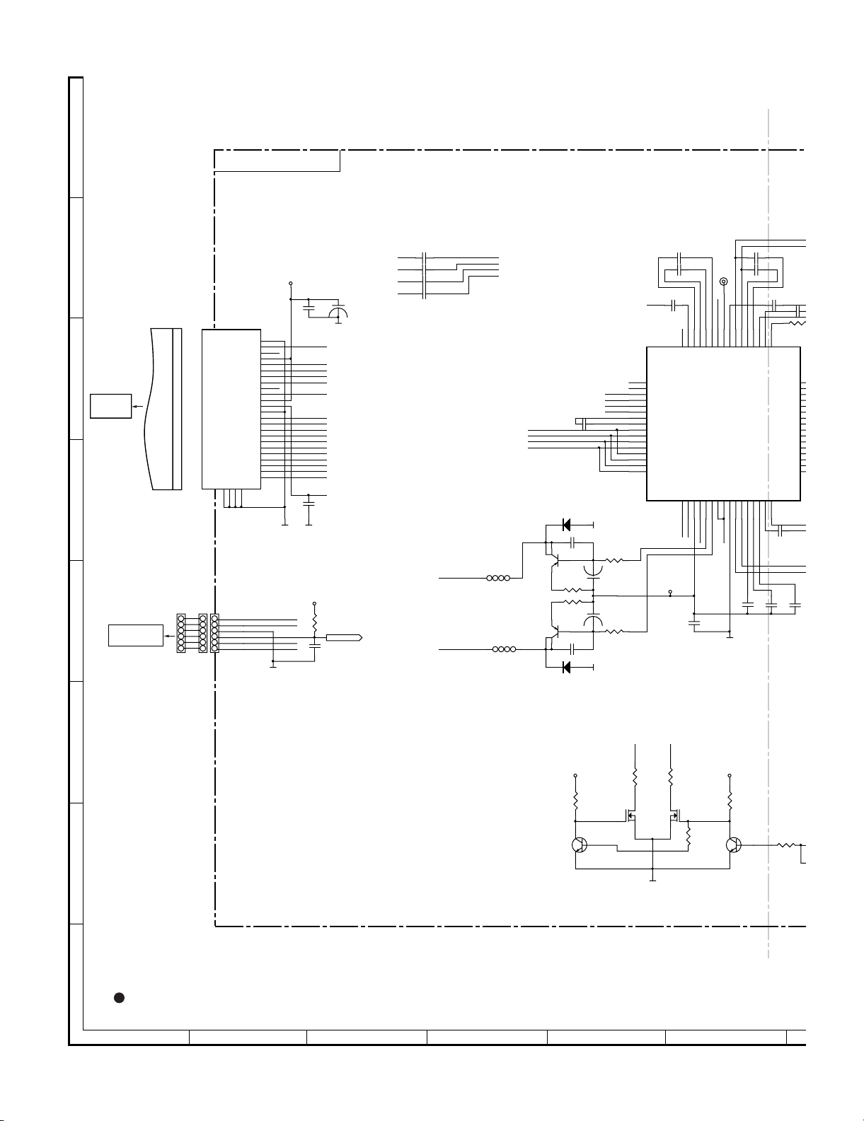
XL-DV60
6
M
1
1
[8] SCHEMATIC DIAGRAM DVD2/3
A
DVD PWB-C (2/3)
B
C
D
E
TO
PICKUP UNIT
ASS'Y
6-2 3-D~G
DVD MECHANISM
6-2 5-E
PWB
C146
A
0.0022
B
C147
RF50V
C15
100/16
C45
+
DVDLDO
PD
CDLDO
VRDVD
VRCD
E
F
D
A
RFOUT
CD-DVD
B
C
TRACK+
TRACKFOCUS+
FOCUS-
RFGND RFGND
MVCC
SW
0.1
RFGND
PVC
C41
0.1
OPEN
HOMESW
OPEN
24
FFC1B
1
CNW4
1
TO
2
3
4
5
6
JB1
24
GND-LD
23
DVD-LD
22
NC
21
HFM
20
MD
19
CD-LID
18
VR(DVD)
17
VR(CD)
16
NC
15
E
14
(VCC)
13
Vc(Vref)
12
GND-PD
11
F
10
B
9
A
8
RFOUT
7
CD/DVDSW
6
D
5
C
4
TR-
3
TR+
2
FO+
1
FO-
GND
GND
GND
GND
27
282625
J4
1
2
3
4
5
6
LOAD-/DCMO-
1
LOAD+/DCMO+
2
3
4
SLED-
5
SLED+
6
MGND
0.0022
C
C145
0.0022
D
C144
0.0022
DVDLDO
CDLDO
BB
AA
DD
CC
L10
FB(0805)
FB(0805)
1
2
3
AA
4
BB
5
CC
6
DD
7
RFGND
C156
100/16
C155
100/16
+
R150
RFGND
R152
8
9
10
11
12
13
14
15
16
1K
1K
D
C
B
A
Q11
2SB1132
Q10
2SB1132
L11
4
4
2
3
3
2
D10
RLS4148
R117
10
R116
D11
RLS4148
C152
100P
C135
0.001
1
+
10
1
C134
0.001
C38
0.1
C44
0.1
C150
820P
RFOUT
646362616059585756555453525150
RFDC
RFSIN
DVDFRP
DVDRFN
A2
B2
C2
D2
CP
CN
D
C
B
A
CD_D
CD_C
CD_B
CD_A
CD_F
CD_E
171819202122232425262728293031
F
E
RF50V
AIN
ATOP
ATON
ES6603
VPBVCDVDLD
PVC
CDLD
DVDLD
RF50V
C40
0.1
TP11
RFO
RF5 0V
AIP
VPA
BYP
RFAC
U7
RF AMP.
CDLD
DVDPD
CDPD
VNB
PD
RFGND
DIP
DIN
FNP
FNN
LDON
MIRRMPMB
LDON
MIRR
C142 C
0.0 1
C87
470PF
C86
470PF
VNA
MLPF
MEV
MIN
49
RX
MEVO
32
C43
R153
SDATA
C149
0.033
0.1
SDEN
MNTR
SCLK
LCP
LCN
V125
TPH
DFT
LINK
C151
0.22
C
0.
V33
CE
FE
TE
PI
V25
1
F
R108
Q12
18K
2SK3018
2
3
G
1
G
C
Q14
2N3904
2
B
E
VRDVD
3
D
1
S
R154
100
RFGND
3
1
VRCD
D
S
R76
100
Q13
2SK3018
G
2
CD-DVD
R97
100K
RF50VRF50V
R122
10K
Q15
3
C
2N3904
R123
2
B
E
1
10K
H
NOTES ON SCHEMATIC DIAGRAM can be found on page 6-1
1
23456
Figure 6-11 SCHEMATIC DIAGRAM (10/13)
6 – 11
Page 33

XL-DV60
MP
28
FNP
53
SPDON
SPDON
U8
BA5954FP
DIN
C42
SCSJ
SDATA
SCLK
0.047
C39
0.1
R75
MIRR
LDON
C46
0.1
RFGND
SVREF15
RF50V
TP12
LDON
DIP
TP9
SVREF15
TP5
DEFCT
R14
33
C158
0.1
MGND
SVREF15
RF50V
0.1
SCSJ
SDATA
SCLK
TP4
CEI
FEI
TEI
SBAD
SVREF15
SDEFCT
MNTR
CEI
FEI
TEI
SBAD
0
R164
12K
VCC
SLEGN
FOCUS
R69
6.8 K
FOCUS-
FOCUS+
R161
R159
R157
R158
33K
47K
C163
100P
3.3 K
R86
C159
0.0047
L9
FB(0805)
MVCC
SLED-
MGND
SLED+
1(0805)
1(0805)
C87
470PF
C86
470PF
C43
0.1
RF50V
C143
0.01U
12K(1%)
R153
525150
49
RX
FNN
VNA
MEV
MB
MLPF
MIN
MEVO
293031
32
C142 C148C149
0.01 160P
0.033
SDEN
SDATA
SCLK
MNTR
V125
LINK
C151
0.22
V33
LCP
LCN
V25
TPH
DFT
RFGND
RF33V
48
47
46
45
44
43
42
41
CE
40
FE
39
TE
38
PI
37
36
35
34
33
MEVO
MOTOR DRIVER
1
VINFC
2
CFCERR1
3
CFCERR2
4
VINSL+
5
VINSL-
6
VOSL
7
VNFFC
8
VCC
9
PVCC1
10
PGND
11
VOSL-
12
VOSL+
13
VOFC-
14
VOFC+
GND29GND
MGND
30
STBY
BIAS
VINTK
CTKERR1
CTKERR2
VINLD
PREGND
PVCC2
VNFTK
PGND
VOLD-
VOLD+
VOTK-
VOTK+
MVCC
28
27
26
25
24
23
22
21
20
19
18
17
16
15
D6
RLS4148
R124
10K
R147
12
22K
33K
R162
47K
R160
C162
100P
R77
MVCC
LOAD-/DCMO-
LOAD+/DCMO+
1(0805)
R156C153
1(0805)
R155
TRACK
0
C47
0.1
TRACK-
TRACK+
SPINDLE
MVCC
MGND
C157
+
47/16
Q15
N3904
2
LOAD-/DCMO-
R121
10K
R149
1.5 K
LOAD+/DCMO+
R146
22K
R123
B
CD-DVD-CTR
10K
TP13
CD-DVD-CTR
7
8 9 10 11 12
MGND
R120
10K
R148
1.5 K
R145
22K
MGND
U6
TL3472
AMP.
3
2
R131
MVCC
8
+
-
4
MGND
1M
MVCC
R133
4.7K
1
MDCTL
Figure 6-12 SCHEMATIC DIAGRAM (11/13)
6 – 12
Page 34

XL-DV60
[9] SCHEMATIC DIAGRAM DVD3/3
8
4
8
4
8
4
VCCV
GNDV
GNDV
2
5
6
9
12
15
16
19
V+
V-
GNDA
V+
V-
GNDA
V+
V-
GNDA
C29
SE_RGB
DAC_MD
DAC_MC
ML1196
U4A
U4B
4558
AMP.
0.1
U4
U5
1
(A,B)
4558
AMP.
1
7
C125
150P
150P
C127
150P
(CH)
(CH)
C126
(CH)
A
B
C
D
CNW2
1
TO
6-3 2-D
2
3
4
5
6
7
MAIN PWB
CNP807
E
F
G
DVD PWB-C (3/3)
10µH
VCCA
ML1196
DAC_MC
DAC_MD
MCLK
TBCK
TWS
TSD0
TSD1
TSD2
+12V
R46 R47 R48
OPEN
J2
+12V1
1
1
VCC1
2
2
GND
3
3
SVCC1
4
4
RFGND
5
5
VCCA1
6
6
GNDA1
7
7
Q3
AMS1117
3.3V REGULATOR
VCC
IN3OUT
OUT
ADJ
1
(EZ1085)
SVCC
+
C7
100/16
GND
R39
0(0805)
R38
0(0805)
L21
+
C13
10/16
GND
R9
R8
R6
R7
R12
R13
R11
R10
OPEN OPEN
L2
L3
L5
R74
R49
3.3
2
4
GND GND
AMS1117
IN
3
Q2
1
MGND
RFGNDGND
AUDIO D/A CONVERTER
1
C34
0.1
11
12
13
33
14
33
9
8
10
2
33
3
33
4
33
5
33
6
33
7
33
K
K1
A
GNDA
FB(0805)
FB(0805)
FB(0805)
OPEN
L6
FB(0805)
VCC33
1
R3
412(1%)
+
R1
681(1%)
2
OUT
4
OUT
ADJ
GND
R182
WM8746
DVDD
DGND
LATCH/12S
SCLK/IWL
SDIN/DM0
MUTE
MODE
LRCLK2
MCLK
BCLK
LRCLK
DIN0
DIN1
DIN2
VCCA
D5
OPEN
A1
+12V
VCC
SVCC
GNDA
VCCA
R37
1
OPEN
C2
100/16
C21 C122
0.1
220/16
R4
412(1%)
R2
681(1%)
0
U1
C1
+
2
+
+12V
AVDD1
AVDD2
AGND1
AGND2
GR0
GR1
GR2
OUT0L
OUT0R
OUT1L
OUT1R
OUT2L
OUT2R
CAP
100uF/16V
2
D4
1N4001
1N4001
AK
VD33D
SVCC
D3
C123
220/16
C8
GND
+
+
R115
15
28
20
24
26
22
18
25
27
21
23
17
19
16
GND
100/16
+
100/16
10
VCC
GND
C12
C31
0.1
RLS4148
C121
+
AMS1117
IN3OUT
+12VA
GNDA
C23
0.1
TP1
TP2
TP3
C26
0.1
D2
220/16
Q1
R35
3.3 (0805)
100/16
FB(0805)
100/16
C120
ADJ
C6
L1
GNDA
220/16
+
OUT
1
C3
SL
SR
C
+12V
GNDA
+
C11
100/16
C25
0.1
C99
10/16
10/16
+
2
4
R5
330(1%)
R36
249(1%)
R118
C101
C5
100/16
+
+
10K
VCCA
GNDA
10/16
+
PLL33V
PLLGND
RFGND
GNDA
+
+
C103
+
C100
10/16
RF33V
+
SVCC
R119
10K
10/16
VCC20
470P
(CH)
C19
0.1
C102
GND
C85
+
+6V
+
R180
0(0805)
MVCC1
C22
C10
100/16
C4
100/16
0.1
L
R
SUB
VCC
L7
FB(0805)
100/16
L8
FB(0805)
C124
220/16
24C01
+12VA
+
C33
0.1
GNDA
+12VA
C32
0.1
GNDA
C14
LCS1#
10/16
+
GND
C114
10/16
R
C106
10/16
L
C107
10/16
+
C113
10/16
SUB
C111
10/16
RF50V
+
C35
0.1
RFGND
MVCC
+
C36
0.1
MGND
LCS1#
VCC
C98
0.1
+
+
+
C37
0.1
LD[7:0]
+6V
+6V
R109
R110
9.1K
+6V
0.1
9.1K
R111
3.9K
C109
10/16
VCC1
100K
GNDA
GNDA
GNDA
R93
R94
100K
100K
R96
C131
0.001
C132
0.001
C133
0.001
LD0
LD3
LD4
LD5
GND
0.1
GNDA
GNDA
GNDA
+
C108
10/16
R83
3.3K
+
R84
3.3K
+
C112
10/16
R85
3.3K
FB(0805)
100/16
GND
8D TRIGGER
74HC374
3
D0
4
D1
7
D2
8
D3
13
D4
14
D5
17
D6
18
D7
1
OE
11
CLK
C18C20C24C27
0.1
3
2
+12VA
5
6
3
2
U5A
L4
+
C9
R73
0
U3
Q0
Q1
Q2
Q3
Q4
Q5
Q6
Q7
C17
0.1
GND
H
NOTES ON SCHEMATIC DIAGRAM can be found on page 6-1
1
23456
Figure 6-13 SCHEMATIC DIAGRAM (12/13)
6 – 13
Page 35

8
4
8
4
8
4
VCCV
GNDV
GNDV
2
5
6
9
12
15
16
19
U4A
V+
V-
GNDA
U4B
V+
V-
GNDA
V+
V-
GNDA
C29
0.1
SE_RGB
DAC_MD
DAC_MC
ML1196
U4
4558
AMP.
1
7
U5
4558
AMP.
1
(A,B)
C125
150P
(CH)
C126
150P
(CH)
C127
150P
(CH)
C104
10/16
+
R105
18K
C105
10uF/16V
+
R106
18K
C110
10/16
+
R107
18K
CDAC
YDAC
UDAC
FDAC
VDAC
GNDV
GNDV
GNDV
GNDV
R91
100K
R92
100K
R95
100K
DVD/CD AUDIO SIGNAL
R_OUT
C128
22P
(CH)
GNDAGNDA
L_OUT
C129
22P
(CH)
GNDAGNDA
SUB_OUT
C130
22P
(CH)
GNDAGNDA
C96 C97
220P
(CH)
C92
OPEN
C90
220P
(CH)
C89
220P
(CH)
C94 C95
220P
(CH)
R173
R171
R170
R169
R172
R112
10
R113
10
R114
10
82
82
82
82
82
L26
2.4µH
L24
2.4µH
L23
2.4µH
L27
2.4µH
L25
2.4µH
SPDIF
GNDA
C188
0.001
GND
YGND
VCC
R129
10M
12
C141
0.1
13 12
56
470P
(CH)
GNDVGNDV
C93
OPEN
GNDVGNDV
C88
470P
(CH)
GNDVGNDV
C91
470P
(CH)
GNDVGNDVGNDV
470P
(CH)
GNDVGNDV
VCCV
C189
OPEN
U2A
U2C
R130
1M
U2F
SE_RGB
M1 M2 M3 M4
M5 M6 M7 M8
M9 M10 M11 M12 M13 M14 M15 M16
mark dot
U2
(A~F)
LOGIC
7404
U2E
11 10
U2D
98
U2B
3
OPEN
R51
VCCV
VCCV
VCCV
VCCV
VCCV
OPEN
R62
OPEN
R61
OPEN
R52
R41
0
Q7
OPEN
R53
75(0805)
R54
75(0805)
R43
OPEN
2
Q5
2N2907
OPEN
R55
OPEN
R56
R42
0
Q4
OPEN
R57
OPEN
R58
OPEN
R45
0
2
Q8
OPEN
R59
OPEN
R60
OPEN
R44
0
2
Q6
OPEN
R132
OPEN
Q9
OPEN
13
2
2
4
1
2
3
GNDV
1
3
GNDV
1
3
GNDV
1
3
GNDV
1
3
GNDV
C28
OPEN
GNDV
M17 M18 M19 M20
M21 M22 M23 M24
VIDEO OUTPUT TABLE
U WARD
VDAC
CVBS CVBS CVBS CVBS
Y
YDAC
CDAC
UDACYCr/Pr
C
FDAC
VCC
OPTICAL
1
R40
GND
68
GNDV
AK
R183
OPEN
RLS4148
L12
FB
L13
FB
L14
FB
L15
FB
L16
FB
Cb/Pb
R181
XGND
L18
L19
L17
0
H WARD
Y
C
FB
FB
FB
AK
D9D8
RLS4148
CDAC2
G/Y
UDAC2
C/cvbs
CVBS
G
R
B
CVBS
C187
0.001
RGB_S
L_OUT
GNDA
R_OUT
SUB_OUT
CVBS
G/Y
C/cvbs
UDAC2
CDAC2
CNW1
J1
1
1
2
2
3
3
4
4
J3 CNW3
12
12
11
11
10
10
9
9
8
8
7
7
6
6
5
5
4
4
3
3
2
2
1
1
TUNER PWB
1
2
3
4
12
11
10
9
VIDEO TERMINAL
8
7
CNP904A
6
5
4
3
2
1
TO
CNP904
6-6 8-A
TO
PWB
6-2 5-B
XL-DV60
7
8 9 10 11 12
Figure 6-14 SCHEMATIC DIAGRAM (13/13)
6 – 14
Page 36

XL-DV60
CNS101
CNW101
CNW102
RED LINE
CNW5
CNP904A
CNP501
CNP802
CFW701B
CFW701A
7654321
7654321
4321
4321
4321
CNW4
RD
BK
RD
BK
WH
4321
RD
BK
WH
WH
WH
WH
WH
WH
13579111315
2 4 6 8 1012 14
78 9654321
78 9654321
7654321
7
6
5
4
4
3
2
1
3
2
1
1
2
3
4
5
6
1
2
3
4
5
6
1
2
3
4
5
6
CNW3
CNW1
CNW2
BK
GY
GY
GY
GY
GY
GY
GY
GY
GY
GY
WH
BK
WH
BK
7
8
9
10
11
12
1
2
3
4
5
6
7
8
9
10
11
12
1
2
3
4
5
6
7
8
9
10
11
12
1
2
3
4
5
6
12345
6789
101112
7
6
5
4
3
2
1
CNS102
RED LINE
7
6
5
4
3
2
1
7
8
6
5
4
3
2
1
CNS302
CNW302
RED LINE
BK
CFW751
CFW750
1
1
2
2
TO
CHASSIS
7
8
9
10
6
5
4
3
2
1
7
8
9
6
5
4
3
2
1
SOLENOID
(124)
MOTOR
(125)
CD CHANGER PWB ASS'Y(132)
SWITCH PWB ASS'Y(133)
WH-LINE
DISPLAY PWB-B1
SWITCH PWB-B4
1515
11
FC501
1
2
4
6
8
10
12
14
3
5
7
9
11
13
15
DVD PWB-C
SPINDLE
MOTOR
SLED
MOTOR
+
1
RD
1
1
24
24
1
24
1
24
BK
23456
-
SWITCH
PICKUP UNIT ASS'Y
DVD MECHANISM UNIT ASS'Y(220)
DVD MECHANISM PWB
FFC1B
J1
J2
J3
JB1
J4
J5
VIDEO TERMINAL PWB-B2
AC 120V,60Hz
AC POWER SUPPLY CORD
[10] WIRING SIDE OF PWB
Figure 6-15 WIRING SIDE OF PWB (1/15)
6 – 15
Page 37

COLOR TABLE
BR
BROWN
RD(R)
OR
ORANGE
YL
YELLOW
GR
GREEN
BL
VL
VIOLET
GY
WH(W)
WHITE
BK
BLACK
PK
RED
BLUE
GRAY
PINK
CNP904
XL-DV60
1
2
3
4
5
6
CNP302
7
8
9
TUNER PWB-A2
234567
1
CNP602
1
2
3
4
7654321
M201(218-4)
CNW2
WH
7654321
7654321
GY
7654321
CNP103B
FAN MOTOR
CNW208
123
WH
BK
CNP201
123
321
CNP208
CNP103A
7654321
CNP102
321
4321
CNW207
CNP205
765
RD
BK
1314 1211 10
1312 1110
CNP206
RED
BK
GYGYGYGYGY
CNW103
MR101
CORE
1234567
CNS602
2134567
BK
RD
BK
WH
RED LINE
BK
BK
RD
WH
12345678
987654321
987654321
1312 1110
987654321
CNW602
CNS206
MAIN PWB-A1
CNP202
312
123
CNS201
67
12345
CNP807
CNP204
321
1
2345
T201
POWER
TRANSFORMER
(MAIN)
CNP101
CNP203
789
654321
CNW201
123
3
2
1
MR201
CORE
BK
RD
JACK PWB-B3
POWER AMP. PWB-D
CNW206
CNW205
1413 1211 10
1514 1312 11 10
1413 1211 10
987654321
987654321
987654321
CNS205
RD
BR
Figure 6-16 WIRING SIDE OF PWB (2/15)
6 – 16
YL
5
YL
4
WH
3
OR
2
BR
1
YL
1
RD
2
YL
3
Page 38

XL-DV60
E
[11] WIRING SIDE OF PWB MAIN TOP/POWER AMP./JACK
A
MAIN PWB-A1 (TOP VI
B
C
D
E
F
G
POWER AMP. PWB-D
Lead-free solder indication
H
Lead-free solder is used in there MAIN, POWER AMP., JACK PWB ( From Serial No.503040001).
Refer to "Precautions for handling lead-free solder" for instructions
and precautions.
1
23456
Figure 6-17 WIRING SIDE OF PWB (3/15)
6 – 17
Page 39

PVIEW)
XL-DV60
JACK PWB-B3
7
8 9 10 11 12
Figure 6-18 WIRING SIDE OF PWB (4/15)
6 – 18
Page 40

XL-DV60
[12] WIRING SIDE OF PWB MAIN BOTTOM
A
B
C
C216
D
E
F
G
Lead-free solder indication
Lead-free solder is used in the MAIN PWB (From Serial No.503040001).
H
Refer to "Precautions for handling lead-free solder" for instructions
and precautions.
1
23456
Figure 6-19 WIRING SIDE OF PWB (5/15)
6 – 19
Page 41

MAIN PWB-A1 (BOTTOM VIEW)
XL-DV60
7
8 9 10 11 12
Figure 6-20 WIRING SIDE OF PWB (6/15)
6 – 20
Page 42

XL-DV60
[13] WIRING SIDE OF PWB TUNER
A
B
C
TUNER PWB-A2 (TOP VIEW
1
D
TUNER PWB-A2 (BOTTOM VIEW
E
F
G
Lead-free solder indication
H
1
Lead-free solder is used in the TUNER PWB (From Serial No.503040001).
Refer to "Precautions for handling lead-free solder" for instructions
and precautions.
23456
Figure 6-21 WIRING SIDE OF PWB (7/15)
6 – 21
Page 43

IEW)
XL-DV60
IEW)
1
7
8 9 10 11 12
Figure 6-22 WIRING SIDE OF PWB (8/15)
6 – 22
Page 44

XL-DV60
[14] WIRING SIDE OF PWB DISPLAY/SWITCH
A
B
DISPLAY PWB-B1 (TOP VIEW)
C
D
E
F
G
SWITCH PWB-B4
Lead-free solder indication
H
Lead-free solder is used in the DISPLAY,SWITCH PWB(From Serial No.503040001).
Refer to "Precautions for handling lead-free solder" for instructions
and precautions.
1
23456
Figure 6-23 WIRING SIDE OF PWB (9/15)
6 – 23
Page 45

DISPLAY PWB-B1 (BOTTOM VIEW)
XL-DV60
1
1
7
8 9 10 11 12
Figure 6-24 WIRING SIDE OF PWB (10/15)
6 – 24
Page 46

XL-DV60
7
R26
R29
(
[15] WIRING SIDE OF PWB DVD TOP
A
R23
J2
R95
C188
R92
C120
R46
R118
C11
C104
C110
R30
R31
C18
R32
R33
R34
C17
L3
L5
L6
R49
85
14
C32
8
C127
14
R99
R47
R119
U4U5
R100
R101
R102
R103
R104
R94
5
B
J5
C
D
E
F
C5
C105
R113
C129
J1
R114
C130
G
R180
C1
R96
Q3
DVD PWB-C
C22
R81
R141
53
0A
C4
U10
R27
R28
208
10
20
30
40
50
5
10
15
20
8
6
R142
R143
R144
L34
C80
C119
TP13
D6
TP14
190
200
U9
60 70 80
U15
U14
NOT USED
L30
C
R25
180
C121
C132
C33
R21
R106
C126
R112
C128
R85
R110
R84
R91
R107
U12
C20
C62
C117
L32
28
30
35
40
45
50
54
L31
C116
C60
C125
R83
R105
C131
R109
R93
R111
C133
QPWBSA005SJZZ
R1
R3
C2
C8
D2
D5
R48
C10
C31
C107
C109
C114
C108
C106
C113
C112
C111
D3
R37
U13
R128
NOT USED
D4
C12
G1
R98
C175
27
25
20
R19
15
R18
R24
10
R20
5
1
L33
L35
RN3
RN2
RN1
Q1
C174
XOUT
R16
R36
R5
1
4
R71
R70
C139
1
R17
R22
52
C118
1
U11
24
Lead-free solder indication
H
Lead-free solder is used in the DVD PWB(From Serial No.503040001).
Refer to "Precautions for handling lead-free solder" for instructions
and precautions.
1
23456
Figure 6-25 WIRING SIDE OF PWB (11/15)
6 – 25
Page 47

-C (TOP VIEW)
R168
R165
R175
R167
170
Q2
R166
C49
C7
R26
3
D6
R29
R25
14
180
U9
80 90 100
48
45
15
40
35
30
C115
R50
25
C51
R151
160
104
C154
R125
150
140
130
120
110
10
R79
R127
XL-DV60
C157
R124
R160
C158
R14
R162
R82
C52
R176
C179
C16
C13
C34
R9
R8
C160
C99
R77
C161
R126R163
D7
1
14
R4
C21
R2
C122
R174
C177
C53
157
105
1
156
5
L28
C180
C85
R178
C48
C24
U3
C167
R137
R139
R177
C56
C101
R35
C170
C6
C169
C168
20
15
11
R164
C123
TRACK
C3
L1
C19
C140
C138
C137
C136
L21
5
10
C103
C162
R147
SLEGN
L7
R179
Q21
C50
R90
R89
R87
R88
25
U1
20
L8
TP26
FOCUS
MIRR
C102
28
15
C25
C124
C37
LDON
SBAD
FEI
CEI
C153
C166
C165
C164
C23
TP2
TP1
TP3
C100
R69
R161
C14
TEI
R159
TP5
R172
R171
R169
R170
R173
C26
C29
L4
R86
R75
TP9
TP4
28
25
5
C159
1
C163
Q10 Q11
C155
C151
TP23
C94
C92 C93
C89
C90
C96
C156
33
48
C35
C87
Q17
Q19
Q18
Q20
Q16
C135
C134
R116
R150
32
35
40
45
50 55 60
49
L25
L24
L27
L23
L26
C9
U7
TP17
C95
C91
C88
C97
R183
C98
U8
L9
202530
Q6
Q5
Q8
Q4
Q7
R152
17
15
10
5
C38
R123
R108
R117
C40
64
TP11
2022
10
16
1
R130
C141
R62
R145
C36
R146
R122
R97
R153
1
D8
D9
15
14
Q15
Q14
7
R133
C147
C86
C143
R59
R44
R53
R57
R45
R55
R51
R41 R42 R43
8
1
Q13
Q12
C146
C43
U2
R61
RFO
C144
C44
U6
R131
R149
R76
R154
C145
C150
R129
14
8
R132
C47
R40
L17
R181
C187
5
4
24
R120
R121
R148
L11
1
C27
L14
C28
Q9
J4
R182
C15
L10
JB1
L18L19
L16
L13
L15
L12
J3
7
8 9 10 11 12
Figure 6-26 WIRING SIDE OF PWB (12/15)
6 – 26
Page 48

XL-DV60
7
8
O
[16] WIRING SIDE OF PWB DVD BOTTOM
A
DVD PWB-C (B
B
SLEG+
SLEG-
SW
MGND
LOAD+
LOAD-
C
VRCD
VRDVD
DVDLDO
RF50V
C45
D
E
F
CD-DVD
FOCUS+
VCC
OPTI
GND
GNDV
CVBS
GNDV
G/Y
C/V
GNDV
UDAC
CDAC
RGB/S
CDLDO
C41
D
TRACK-
TRACK+
FOCUS-
R156
R157
R158
D10
E
PD
PVC
C
RFGND
D11
R60
R54
R58
R56
R52
F
A
B
RFOUT
R155
C152
R64
C190
C46
C142
C149
C57
C148
C39
R134
R12
R136
R13
R138
R11
R135
R10
R140
R6
C172
C173
C171
C55
C42
C81
C75
R7
C84
C77
C58
C176
C178
C54
C
C7
G
Lead-free solder indication
H
Lead-free solder is used in the DVD PWB(From Serial No.503040001).
Refer to "Precautions for handling lead-free solder" for instructions
and precautions.
1
23456
Figure 6-27 WIRING SIDE OF PWB (13/15)
6 – 27
Page 49

B-C (BOTTOM VIEW)
XL-DV60
C54
C173
C178
C171
C176
C71
C78
C82
C79
C76
C72
C74
C83
C69
C73
C68
C70
R80
R78
C63
C65
C66
C61
R15
C67
C64
C182
C183
C181
C184
C185
C186
R73
R38
R39
C189
R74
STB
CLID
BUSY
CLK
DI
DO
GND
+12V1
VCC1
GND
SVCC1
RFGND
VCCA1
GNDA1
L2
R115
L
C59
8
7
8 9 10 11 12
GNDA
R
SUB
Figure 6-28 WIRING SIDE OF PWB (14/15)
6 – 28
Page 50

XL-DV60
[17] WIRING SIDE OF PWB VIDEO TERMINAL
A
B
VIDEO TERMINAL PWB-B2 (TOPVIEW)
C
D
E
VIDEO TERMINAL PWB-B2 (BOTTOM VIEW)
F
G
Lead-free solder indication
H
Lead-free solder is used in the
Refer to "Precautions for handling lead-free solder" for instructions
and precautions.
1
VIDEO TERMINAL
PWB(From Serial No.503040001).
23456
Figure 6-29 WIRING SIDE OF PWB (15/15)
6 – 29
Page 51

XL-DV60
CHAPTER 7. FLOWCHART
[1] TROUBLESHOOTING
1. When the CD does not function
The CD section may not operate when the objective lens of the optical pickup is dirty. Clean the objective lens, and check the playback operation.
When this section does not operate even after the above step is taken, check the following items.
Remove the cabinet and follow the trouble shooting instructions.
"Track skipping and/or no TOC (Table Of Contents) may be caused by build up of dust other foreign matter on the laser pickup lens. Before attempting
any adjustment make certain that the lens is clean. If not, clean it as mentioned below."
Turn the power off.
Gently clean the lens with a lens cleaning tissue and a small amount of isopropyl alcohol.
Do not touch the lens with the bare hand.
Parts code
1. CD optical pickup Lens cleaner disc UDSKA0004AFZZ
HOW TO USE
1.
Using the brush in the cleaner cap, apply 1 or 2 drops of the cleaning fluid to the
brush on the CD cleaner disc which has the mark next to it.
2.
Place the CD cleaner disc onto the CD disc tray with the brush side down,then
press the play button.
3.
You will hear music for about 20 seconds and the CD player will automatically stop.
If it still play continuously, press the stop button.
Cleaning fluid
CAUTION
The CD lens cleaner should be effective for 30-50 operations, however if the
brushes become worn out earlier then please replace the cleaner disc.
If the CD cleaner brushes become very wet then wipe off any excess fluid with a soft
cloth.
Do not drink the cleaner fluid or allow it contact with the eyes. In the event of this
happening then drink and / or rinse with clean water and seek medical advice.
The CD cleaner disc must not be used on car CD players or on computer CD-ROM
drives.
All rights reserved. Unauthorized duplicating, broadcasting and renting this product
is prohibited by law.
2. When a DVD/CD cannot be played
2.1. Pressing the DVD/CD operation key is accepted, but playback does not occur.
1) Focus-HF system check
2) Tracking system check
3) Spin system check
4) Others
Cleaner disc
7 – 1
Page 52

XL-DV60
Stop
Stop
(1) Focus-HF system check.
Although a DVD/CD is inserted and the cover is closed,
"NO DISC" is displayed.
Press the OPEN/CLOSE switch (SW717) without inserting a
disc, and try starting the playback operation.
1. Does the pickup move to the PICKUP-IN Switch position? No Sled motor.
Yes
2. Does the focus (lens) move up and down?
(Waveform drawing Figure 1)
No Check the focus peripheral circuit.
Figure 1
Yes
3. Is the laser lit? No Check the laser diode driver Q10,Q11 peripheral circuit.
Yes
4. Is the turntable rotating? No Spindle motor.
When a disc is loaded, start playback operation.
1. Is focus servo activated?
(Waveform drawing Figure 2)
3. Is the HF waveform normal?
(Waveform drawing Figure 3)
Stop
Yes
No Pins 39~41, 79 and 63 on U7.
Check the laser diode driver Q10,Q11 peripheral circuit.
No If the level is not normal.
Figure 2
Figure 3
7 – 2
Page 53

(2) Tracking system check.
Stop
Stop
Check the TE waveform at pin 39 on U7.
If the waveform shown in Figure 4 appears and soon after NO
DISC appears?
No
"Initialization" is possible, but play is not possible?
No
"Initialization" is not possible.
Check the J5 connect well
or not
Yes
Yes
XL-DV60
The tracking servo is not activated.
Check the peripheral circuits at pin 39 on U7, and Pin 145 on
U9 and FFC1B.
Check the CNP802 and J5 connect well or not.
(3) Spin system check.
Press the OPEN/CLOSE switch without inserting a disc, and
then try starting the play operation.
1. The turntable rotates a little?
(Waveform drawing Figure 5)
No
2. The turntable doesn't rotate. Check around pins 17,18 on U8.
Yes
The spin driver circuit is OK.
Figure 4
7 – 3
Figure 5
Page 54

XL-DV60
(4) Others.
When toc can read out and play normal, but no sound, please check as the following steps:
Is the waveform correct?
(Waveform drawing Figure 6)
Yes
Is U1 output L/R and sub woofer normally?
Yes
Is J1 connect correctly?
Yes
Check CNP904 if connect well.
Stop
Check U9.
No
Change U1.
No
Connect J1 well.
No
Figure 6
7 – 4
Page 55

XL-DV60
CHAPTER 8. OTHERS
Service Manual
[1] FUNCTION TABLE OF IC
IC601 VHiLC75341M-1: Signal Control (LC75341M)
IC603 VHiLC75341M-1: Signal Control (LC75341M)
Pin No. Terminal Name Function
1 DI Serial data and clock input pin for con-
trol.
2 CE Chip enable pin.
Data written into an internal latch in a
timing of "H" to "L".
Each analog switch is activated.
Data transfer enabled at "H" level.
3 VSS Ground pin.
4 LOUT Bass band filter comprising
capacitor and resistor connection pin
and bass/treble output pin.
5 LBASS Bass band filter comprising capacitor
and resistor connection pin.
6 LTRE Treble band filter comprising capacitor
and resistor connection pin.
7 LIN Volume + equaliser output pin.
8 LSEL0 Input selector output pin.
9,10*1112L4-1 Input signal pin.
In this unit, the terminal with asterisk mark (*) is (open) terminal which is not connected to the outside.
IC601 VHiLC75341M-1: Signal Control (LC75341M)
IC603 VHiLC75341M-1: Signal Control (LC75341M)
Pin No. Terminal Name Function
13,14,
15*,16
17 RSEL0 Input selector output pin.
18 RIN Volume + equaliser output pin
19 RTRE Treble band filter comprising capacitor
20 RBASS Bass band filter comprising capacitor
21 ROUT Bass band filter comprising capacitor
22 VREF 0.5x VDD voltage generation block
23 VDD Supply pin
24 CL Serial data and clock input pin for con-
R1-4 Input signal pin.
XL-DV60
and resistor connection pin.
and resistor connection pin.
and resistor connection pin and bass/
treble output pin.
for analog ground. Capacitor of several 10µF to be connected between
VREF and AWSS (VSS) as a countermeasure against power ripple.
trol.
L4
L3
L2
L1
R1
R2
R3
R4
10
11
12
13
14
15
16
LOUT
LSEL0
LIN
LTRE
LBASS
45678
9
VSS
3
2
1
24
23
22
CE
DI
CL
VDD
VREF
1817
CONTROL
CIRCUIT
LOGIC
CIRCUIT
CONTROL
CIRCUIT
19
LVref
CCB
INTERFACE
RVref
20 21
RIN
RSEL0
Figure 1 BLOCK DIAGRAM OF IC
RTRE
8 – 1
RBASS
ROUT
Page 56

XL-DV60
IC701 RH-iXA009SJZZ: System Microcomputer (IXA009SJ)
Pin No. Port Name Input/Output Function
14,89 VSS1,VSS2 - • Power supply (-)
17,90,
46,72
51 FIX0 - • Test Pin
85,86,87,
88,91,92,
93*,94
1,2,95,96,
97,98,99,
100*
3*,4*,5*,6,
7,8,9*,10*
VDD1,VDD2,
VDD3,VDD4
PORT0 P00 to
P07
PORT1 P10 to
P17
PORT3 P30 to
P37
- • Power supply (+)
Set as VSS with the user’s option. (Note1)
I/O • 8bit input/output port
• data direction programmable in nibble units
• Use of pull-up resistor can be specified in nibble units
• Input for HOLD release
• Input for port 0 interrupt
• 14V withstand at N-channel open drain output
I/O • 8bit input/output port
• data direction programmable for each bit
• Use of pull-up resistor can be specified for each bit
• Other pin functions
P10: SIO0 data output
P11: SIO0 data input / bus input / output
P12: SIO0 clock input / output
P13: SIO1 data output
P14: SIO1 data input / bus input / output
P15: SIO1 clock input / output
P16: Timer 1 PWML output
P17: Timer 1 PWMH output / Buzzer output
I/O • 8bit Input/output port
• Data direction can be specified for each bit
• Use of pull-up resistor can be specified for each bit
• 14V withstand at N-channel open drain output
• Other functions:
P30-P33:
P34- 37:
• The following types of interrupt detection are possible:
INT4 input / HOLD release input / Timer 1 event input / Timer 0L capture input / Timer
0H capture input
INT5 input / HOLD release input / Timer 1 event input / Timer 0L capture input / Timer
0H capture input
INT4 Yes Yes Yes N o No
INT5 Yes Yes Yes N o No
Rising Falling Rising/
Falling
H level L level
26,27,
28*,29
18,19,20,
21*,22*,
23,24,25
30,31,32,
33,34,35,
36,37,38
PORT7 P70 to
P73
PORT8 P80 to
P87
S0/T0 to S8/
T8
I/O • 4bit input/output port
I/O • 8bit input/output port
O • Large current output for VFD display controller digit (can be used for segment)
• Data direction can be specified for each bit
• Use of pull-up resistor can be specified for each bit
• Other functions
P70:
P71
P72:
P73:
AD input port: AN8(P70), AN9(P71), AN12(P72), AN13(P73)
The following types of interrupt detection are possible:
• Input/output can be specified in a bit unit
• Other functions:
AD input port: AN0 to AN7
Weak signal detector input port: MICIN(P87)
INT0 input / HOLD release input / Timer0L capture input / Output for watchdog timer
INT1 input / HOLD release input / Timer0H capture input
INT2 input / HOLD release input / Timer 0 event input / Timer0L capture input / High
speed clock counter input
INT3 input(noise rejection filter attached input) / Timer 0 event input /Timer 0H capture
input
Rising Falling Rising/
Falling
INT0 Yes Yes No Ye s Yes
INT1 Yes Yes No Ye s Yes
INT2 Yes Yes Yes N o No
INT3 Yes Yes Yes N o No
H level L level
8 – 2
Page 57

Pin No. Port Name Input/Output Function
39,40,
41*,42,43,
S9/T9 to S15/
T15
O • Large current output for VFD display controller segment/digit
44,45
47,48,49,
50,52,53,
54,55
56,57,58,
59,60,61,
62,63
64,65,66,
67,68,69,
70,71
73,74,75,
76,77,78,
79,80
81*,82*,
83,84*
S16 to S23 I/O • Output for VFD display controller segment/digit
• Other functions:
High voltage input port: PC0 to PC7
S24 to S31 I/O • Output for VFD display controller segment
• Other functions:
High voltage input port: PD0 to PD7
S32 to S39 I/O • Output for VFD display controller segment
• Other functions:
High voltage input port: PE0 to PE7
S40 to S47 I/O • Output for VFD display controller segment
• Other functions:
High voltage input/output port: PF0 to PF7
S48 to S51 I/O • Output for VFD display controller segment
• Other functions:
High voltage input/output port: PG0 to PG7
11 RES I Reset terminal
12 XT1 I • Input for 32.768kHz crystal oscillation
• Other functions:
General purpose input port
When not in use, connect to VDD1.
AD input port: AN10
13 XT2 I/O • Output for 32.768kHz crystal oscillation
• Other functions:
General purpose input/output port
When not in use, set to oscillation mode and leave open circuit.
AD input port: AN11
15 CF1 I Input terminal for ceramic oscillator
16 CF2 O Output terminal for ceramic oscillator
In this unit, the terminal with asterisk mark (*) is (open) terminal which is not connected to the outside.
Note1:) The LC876700 series can be mounted onto the circuit board of the LC 876500, LC876600 series.
In this case, the fluorescent character display tube power voltage (minus voltage) is supplied to the FIX0 pin. This would not cause any
error.
IC701 RH-iXA009SJZZ: System Microcomputer (IXA009SJ)
XL-DV60
S48/PG0
S49/PG1
S50/PG2
S51/PG3
P00
P01
P02
P03
VSS2
VDD2
P04
P05
P06
P07
P10/SO0
P11/SI0/SB0
P12/SCK0
P13/SO1
P14/SI1/SB1
P15/SCK1
S47/PF7
S46/PF6
S45/PF5
S44/PF4
S43/PF3
S42/PF2
S41/PF1
S40/PF0
VDD4
S39/PE7
S38/PE6
S37/PE5
S36/PE4
S35/PE3
S34/PE2
S33/PE1
S32/PE0
S31/PD7
S30/PD6
S29/PD5
S28/PD4
S27/PD3
S26/PD2
S25/PD1
S24/PD0
8079787776757473727170696867666564636261605958575655545352
81
82
83
84
85
86
87
88
89
90
91
92
93
94
95
96
97
98
99
100
1234567891011121314151617181920212223242526272829
P16/T1PWML
P30/INT4/T1IN
P31/INT4/T1IN
P17/T1PWMH/BUZ
RH-IXA009SJZZ
RES
P32/INT4/T1IN
P33/INT4/T1IN
P34/INT5/T1IN
P35/INT5/T1IN
P36/INT5/T1IN
P37/INT5/T1IN
CF1
VSS1
XT1/AN10
XT2/AN11
CF2
VDD1
P80/AN0
P81/AN1
P82/AN2
P83/AN3
P84/AN4
P85/AN5
P86/AN6
P87/AN7/MICIN
Figure 2 BLOCK DIAGRAM OF IC
S23/PC7
S22/PC6
S21/PC5
S20/PC4
FIX0
51
50
49
48
47
46
45
44
43
42
41
40
39
38
37
36
35
34
33
32
31
30
S0/T0
P73/INT3/AN13
P72/INT2/T0IN/AN12
P70/INT0/T0LCP/AN8
P71/INT1/T0HCP/AN9
S19/PC3
S18/PC2
S17/PC1
S16/PC0
VDD3
S15/T15
S14/T14
S13/T13
S12/T12
S11/T11
S10/T10
S9/T9
S8/T8
S7/T7
S6/T6
S5/T5
S4/T4
S3/T3
S2/T2
S1/T1
8 – 3
Page 58

XL-DV60
IC702 VHiAT24C04/-1:EEPROM (AT24C04)
Pin No. Terminal Name Function
1*,2*,3* A0-A2 Address Inputs
4 GND Ground
5 SDA Serial Data
6 SCL Serial Clock Input
7* WP Write Protect
8 VCC Power
In this unit, the terminal with asterisk mark (*) is (open) terminal which
is not connected to the outside.
8-lead SOIC
1
A0
2
A1
3
A2
GND
4
Figure 3 BLOCK DIAGRAM OF IC
VCC
8
WP
7
SCL
6
SDA
5
8 – 4
Page 59

[2] FL DISPLAY
VFD701 VVK251116//-1
GRID ASSIGNMENT
ANODE CONNECTION
XL-DV60
OUTER DRAWING
PIN CONNECTION
8 – 5
Page 60

XL-DV60
-MEMO-
8 – 6
Page 61

PARTS GUIDE
DVD MICRO SYSTEM
XL-DV60
CONTENTS
[1] INTEGRATED CIRCUITS
[2] TRANSISTORS
[3] DIODES
[4] FILTERS
[5] TRANSFORMERS
[6] COILS
[7] VARIABLE RESISTORS
[8] VIBRATORS
[9] CAPACITORS
[10] RESISTORS
[11] OTHER CIRCUITRY PARTS
[12] CHANGER MECHANISM PARTS
[13] CABINET PARTS
MODEL
XL-DV60 DVD Micro System consisting of XL-DV60 (main
unit), CP-DV60F (front speakers) and CP-DV60SW(subwoofer).
[14] SPEAKER BOX PARTS
[15] ACCESSORIES
[16] P.W.B. ASSEMBLY (Not
Replacement Item)
[17] OTHER SERVICE PARTS
[18] INTEGRATED CIRCUITS (DVD)
[19] TRANSISTORS (DVD)
[20] DIODES (DVD)
[21] COILS (DVD)
[22] VIBRATORS (DVD)
[23] CAPACITORS (DVD)
[24] RESISTORS (DVD)
[25] OTHER CIRCUITRY PARTS (DVD)
INDEX
XL-DV60
Parts marked with " " are important for maintaining the safety of the set. Be sure to replace these
parts with specified ones for maintaining the safety and performance of the set.
SHARP CORPORATION
This document has been published to be used
for after sales service only.
The contents are subject to change without notice.
Page 62

XL-DV60
NO. PARTS CODE
PRICE
RANK
NEW
MARK
PAR T
RANK
[1] INTEGRATED CIRCUITS
IC101 VHILM4781TA-1 AZ N Power Amp.,LM4781TA
IC201 VHIKIA7805API AF Voltage Regulator,KIA7805API
IC202 VHIKIA7812API AE Voltage Regulator,KIA7812API
IC203 VHILM2576T/-1 AR Voltage Regulator,LM2576T
IC204 VHIAN78L05/-1 AE Constant Voltage Regulator,AN78L05
IC301 VHITA7358AP-1 AG FM Front End,TA7358AP
IC302 VHILC72131/-1 AP PLL (Tuner),LC72131
IC303 VHILA1832S/-1 AN FM IF Det./FM Mpx./AM IF,LA1832S
IC601 VHILC75341M-1 AM Signal Control,LC75341M
IC602 VHINJM4558D-1 AH Buffer Amp.,NJM4558D or AN4558
IC603 VHILC75341M-1 AM Signal Control,LC75341M
IC701 RH-IXA009SJZZ AV System Microcomputer,IXA009SJ
IC702 VHIAT24C04/-1 AH EEPROM,AT24C04
[2] TRANSISTORS
Q101 VS2HC1815GR-1 AB Silicon,NPN,2HC1815 GR
Q102 VS2HC1815GR-1 AB Silicon,NPN,2HC1815 GR
Q107 VS2SC3052F+-1 AD Silicon,NPN,2SC3052F+
Q108 VS2SC3052F+-1 AD Silicon,NPN,2SC3052F+
Q109 VS2HC1815GR-1 AB Silicon,NPN,2HC1815 GR
Q110 VSKRA107M//-1 AE Digital,PNP,KRA107 M
Q111 VSKRC107M//-1 AC Digital,NPN,KRC107 M
Q112 VS2HC1815GR-1 AB Silicon,NPN,2HC1815 GR
Q113 VS2HC1815GR-1 AB Silicon,NPN,2HC1815 GR
Q114 VS2HC1815GR-1 AB Silicon,NPN,2HC1815 GR
Q115 VS2HC1815GR-1 AB Silicon,NPN,2HC1815 GR
Q116 VSKRC107M//-1 AC Digital,NPN,KRC107 M
Q117 VS2SB562-C/-1 AD Silicon,PNP,2SB562 C
Q118 VS2HC1815GR-1 AB Silicon,NPN,2HC1815 GR
Q201 VS2HA1015GR-1 AB Silicon,PNP,2HA1015 GR
Q202 VS2SC535-C/-1 AC Silicon,NPN,2SC535 C
Q203 VSKTC3200GR-1 AC Silicon,NPN,KTC3200 GR
Q204 VS2HA1015GR-1 AB Silicon,PNP,2HA1015 GR
Q205 VS2HC1815GR-1 AB Silicon,NPN,2HC1815 GR
Q206 VS2HC1815GR-1 AB Silicon,NPN,2HC1815 GR
Q207 VS2SC3052F+-1 AD Silicon,NPN,2SC3052F+
Q208 VS2SA1235F+-1 AD Silicon,PNP,2SA1235F+
Q213 VS2SB562-C/-1 AD Silicon,PNP,2SB562 C
Q214 VS2SC3052F+-1 AD Silicon,NPN,2SC3052F+
Q302 VS2SC535-C/-1 AC Silicon,NPN,2SC535 C
Q306 VS2SC535-C/-1 AC Silicon,NPN,2SC535 C
Q351 VSKRC104M//-1 AC Digital,NPN,KRC104 M
Q360 VS2HA1015GR-1 AB Silicon,PNP,2HA1015 GR
Q502 VSKRC102M//-1 AC Digital,NPN,KRC102 M
Q503 VS2SB562-C/-1 AD Silicon,PNP,2SB562 C
Q504 VSKTC3203Y/-1 AC Silicon,NPN,KTC3203 Y
Q505 VSKTA1271Y/-1 AC Silicon,PNP,KTA1271 Y
Q506 VS2HC1815GR-1 AB Silicon,NPN,2HC1815 GR
Q507 VS2HC1815GR-1 AB
Q508 VSKTA1271Y/-1 AC Silicon,PNP,KTA1271 Y
Q509 VSKTC3203Y/-1 AC Silicon,NPN,KTC3203 Y
Q511 VSKTC3203Y/-1 AC Silicon,NPN,KTC3203 Y
Q702 VSKRC102M//-1 AC Digital,NPN,KRC102 M
Q703 VS2HC1815GR-1 AB Silicon,NPN,2HC1815 GR
Q704 VS2HC1815GR-1 AB Silicon,NPN,2HC1815 GR
Q705 VS2HC1815GR-1 AB Silicon,NPN,2HC1815 GR
Silicon,NPN,2HC1815 GR
[3] DIODES
D104 VHD1N4148//-1 AA Silicon,1N4148
D105 VHD1N4148//-1 AA Silicon,1N4148
D106 VHD1N4148//-1 AA Silicon,1N4148
D107 VHD1N4004//-1 AB Silicon,1N4004
D108 VHD1N4148//-1 AA Silicon,1N4148
D109 VHD1N4004//-1 AB Silicon,1N4004
D110 VHD1N4004//-1 AB Silicon,1N4004
D111 VHD1N4004//-1 AB Silicon,1N4004
D112 VHD1N4004//-1 AB Silicon,1N4004
D201 VHDTS6B04GM-1 AP Silicon,TS6B04GM-1
D202 VHD1N4148//-1 AA Silicon,1N4148
D205 VHDKBP304GM-1 AF Silicon,KBP304GM-1
D209 VHD1N4004//-1 AB Silicon,1N4004
D210 VHD1N4004//-1 AB Silicon,1N4004
D211 VHD1N4004//-1 AB Silicon,1N4004
D212 VHD1N4004//-1 AB Silicon,1N4004
D213 VHD1N4004//-1 AB Silicon,1N4004
!
!
!
!
D214 VHD1N4004//-1 AB Silicon,1N4004
D215 VHD1N4004//-1 AB Silicon,1N4004
D216 VHD1N4004//-1 AB Silicon,1N4004
D217 VHD1N4004//-1 AB Silicon,1N4004
D218 VHD1N4004//-1 AB Silicon,1N4004
D219 VHD1N4004//-1 AB Silicon,1N4004
D231 VHD1N5822//-1 AD Silicon,1N5822
D232 VHD1N4004//-1 AB Silicon,1N4004
D301 VHD1N4148//-1 AA Silicon,1N4148
D302 VHD1N4148//-1 AA Silicon,1N4148
DESCRIPTION
2
Page 63

XL-DV60
NO. PARTS CODE
PRICE
RANK
NEW
MARK
PAR T
RANK
[3] DIODES
D305 VHD1N4148//-1 AA Silicon,1N4148
D306 VHD1N4148//-1 AA Silicon,1N4148
D307 VHD1N4148//-1 AA Silicon,1N4148
D308 VHD1N4148//-1 AA Silicon,1N4148
D604 VHD1N4148//-1 AA Silicon,1N4148
D605 VHD1N4148//-1 AA Silicon,1N4148
D701 VHD1N4004//-1 AB Silicon,1N4004
D702 VHD1N4148//-1 AA Silicon,1N4148
D703 VHD1N4148//-1 AA Silicon,1N4148
D704 VHD1N4148//-1 AA Silicon,1N4148
D705 VHD1N4148//-1 AA Silicon,1N4148
D706 VHD1N4004//-1 AB Silicon,1N4004
D708 VHD1N4004//-1 AB Silicon,1N4004
D709 VHD1N4148//-1 AA Silicon,1N4148
D710 VHD1N4148//-1 AA Silicon,1N4148
D712 VHD1N4148//-1 AA Silicon,1N4148
D713 VHD1N4148//-1 AA Silicon,1N4148
LED701 VHPLP3052A+-1 AC LED,Red,LP3052A+
VD301 VHCSVC348S/-1 AK Variable Capacitance,SVC348S
VD302 VHCKDV147B/-1 AH Variable Capacitance,KDV147B
VD303 VHCKDV147B/-1 AH Variable Capacitance,KDV147B
ZD101 VHEDZH06B2+-1 AB Zener,6.2V,DZH06B2+
ZD201 VHEDZH3001+-1 AB Zener,30V,DZH3001+
ZD202 VHEDZH06C2+-1 AB Zener,6.2V,DZH06C2+
ZD351 VHEDZH05C2+-1 AB Zener,5.1V,DZH05C2+
ZD701 VHEDZH03C3+-1 AB Zener,3.3V,DZH03C3+
[4] FILTERS
BF301 RFILRA001SJZZ AD Band Pass Filter
CF302 RFILF0004SJZZ AG FM IF,10.7 MHz
CF303 RFILF0004SJZZ AG FM IF,10.7 MHz
CF351 RFILF0003AWZZ AK FM IF
CF352 RFILA0003SJZZ AF AM IF
[5] TRANSFORMERS
!
!
T201 RTRNPA036SJZZ N Power (Main)
T202 RTRNP0056SJZZ AM Power (Sub)
T302 RCILAA002SJZZ AC AM Antenna
T304 RCILI0005SJZZ AF FM IF
T306 RCILBA006SJZZ AC AM OSC.
T351 RCILI0004SJZZ AF AM IF
[6] COILS
L103 VP-DH100K0000 AB 10 µ H,Choke
L105 VP-DH2R2K0000 AB 2.2 µ H,Peaking
L206 RCILCA001SJZZ AD 100 µ H
L302 RCILR0003SJZZ AD FM RF
L303 RCILB0016SJZZ AD FM OSC.
L351 VP-DH101K0000 AB 100 µ H,Choke
L352 VP-DH101K0000 AB 100 µ H,Choke
L353 VP-DH102K0000 AB 1 mH,Choke
L502 VP-DHR82K0000 AE 0.82 µ H,Choke
L503 VP-DHR82K0000 AE 0.82 µ H,Choke
L601 VP-DH2R2K0000 AB 2.2 µ H,Peaking
L701 VP-DHR82K0000 AE 0.82 µ H,Choke
L702 RCILCA003SJZZ AB 2.4 µ H,Choke
L703 VP-DHR82K0000 AE 0.82 µ H,Choke
L704 VP-DHR82K0000 AE 0.82 µ H,Choke
L705 VP-DHR82K0000 AE 0.82 µ H,Choke
L707 VP-DHR82K0000 AE 0.82 µ H,Choke
L708 VP-DHR82K0000 AE 0.82 µ H,Choke
L901 RCILCA002SJZZ AB 10 µ H
L902 RBLN-A001SJZZ AB Ferrite Bead,120 ohms
L903 RBLN-A001SJZZ AB Ferrite Bead,120 ohms
L904 RBLN-A001SJZZ AB Ferrite Bead,120 ohms
L905 RBLN-A001SJZZ AB Ferrite Bead,120 ohms
L906 RBLN-A001SJZZ AB Ferrite Bead,120 ohms
L907 RBLN-A001SJZZ AB Ferrite Bead,120 ohms
LF201 RCILZ0005SJZZ AF Line Filter
!
[7] VARIABLE RESISTORS
VR351 RVR-M0026AWZZ AC 10 kohm (B),Semi-VR [FM Mute Level]
[8] VIBRATORS
X351 RCRM-0007SJZZ AG VCO,456 kHz
X352 RCRSP0003SJZZ AL Crystal,4.5 MHz
X701 RCRSPA007SJZZ AE Crystal,32.768 kHz
X702 RCRM-0008SJZZ AG Ceramic,8 MHz
DESCRIPTION
3
Page 64

XL-DV60
NO. PARTS CODE
PRICE
RANK
NEW
MARK
PAR T
RANK
[9] CAPACITORS
C101 VCKYCY1HB221K AA 220 pF,50V
C102 VCKYCY1HB221K AA 220 pF,50V
C104 RC-GZA105AF1H AB 1 µ F,50V,Electrolytic
C105 RC-GZA105AF1H AB 1 µ F,50V,Electrolytic
C106 RC-GZA106AF1H AB 10 µ F,50V,Electrolytic
C107 RC-GZA476AF1H AB 47 µ F,50V,Electrolytic
C108 RC-GZA476AF1H AB 47 µ F,50V,Electrolytic
C109 RC-GZA335AF1H AB 3.3 µ F,50V,Electrolytic
C119 VCKYCY1HF223Z AA 0.022 µ F,50V
C120 VCKYCY1HF223Z AA 0.022 µ F,50V
C121 VCKYCY1HF223Z AA 0.022 µ F,50V
C122 VCKYPA1HF223Z AB 0.022 µ F,50V
C123 VCKYPA1HF223Z AB 0.022 µ F,50V
C124 VCKYCY1HF223Z AA 0.022 µ F,50V
C125 VCFYFA1HA104J AC 0.1 µ F,50V,Thin Film
C126 VCKYCY1HB104K AD 0.1 µ F,50V
C127 VCFYFA1HA104J AC 0.1 µ F,50V,Thin Film
C128 VCFYFA1HA104J AC 0.1 µ F,50V,Thin Film
C129 VCKYCY1HB104K AD 0.1 µ F,50V
C130 VCFYFA1HA104J AC 0.1 µ F,50V,Thin Film
C131 VCKYPA1HB472K AB 0.0047 µ F,50V
C132 VCKYPA1HB472K AB 0.0047 µ F,50V
C133 VCKYPA1HB472K AB 0.0047 µ F,50V
C134 RC-GZA336AF1C AB 33 µ F,16V,Electrolytic
C135 RC-GZA106AF1H AB 10 µ F,50V,Electrolytic
C136 RC-GZA106AF1H AB 10 µ F,50V,Electrolytic
C137 VCKYPA1HB104K AC 0.1 µ F,50V
C138 VCKYPA1HB104K AC 0.1 µ F,50V
C139 RC-GZA476AF1H AB 47 µ F,50V,Electrolytic
C140 VCKYCY1HB222K AA 0.0022 µ F,50V
C141 RC-GZA335AF1C AB 3.3 µ F,16V,Electrolytic
C142 RC-GZA476AF1C AB 47 µ F,16V,Electrolytic
C160 VCKYCY1CF105Z AB 1 µ F,16V
C161 VCKYCY1CF105Z AB 1 µ F,16V
C165 VCKYCY1HB472K AA 0.0047 µ F,50V
C167 VCKYCY1HB472K AA 0.0047 µ F,50V
C169 VCKYCY1HB472K AA 0.0047 µ F,50V
C171 VCKYCY1HB221K AA 220 pF,50V
C201 RC-GZA107AF1C AB 100 µ F,16V,Electrolytic
C202 VCKYPA1HF223Z AB 0.022 µ F,50V
C203 VCFYFA1HA104J AC 0.1 µ F,50V,Thin Film
C204 VCFYFA1HA104J AC 0.1
C205 VCFYFA1HA104J AC 0.1 µ F,50V,Thin Film
C206 VCFYFA1HA104J AC 0.1 µ F,50V,Thin Film
C207 RC-GZV227AF1H AC 220 µ F,50V,Electrolytic
C208 RC-GZA476AF1H AB 47 µ F,50V,Electrolytic
C209 RC-GZV337AF1V AB 330 µ F,35V,Electrolytic
C210 RC-GZA107AF1H AC 100 µ F,50V,Electrolytic
C211 RC-GZW478AF1V AH 4700 µ F,35V,Electrolytic
C212 RC-GZW478AF1V AH 4700 µ F,35V,Electrolytic
C213 VCKYPA1HF473Z AB 0.047 µ F,50V
C214 RC-EZW688AF1E AH 6800 µ F,25V,Electrolytic
C215 VCKYPA1HF473Z AB 0.047 µ F,50V
C216 RC-GZA227AF1C AB 220 µ F,16V,Electrolytic
C217 RC-GZA477AF1C AC 470 µ F,16V,Electrolytic
C219 VCKYCY1HF223Z AA 0.022 µ F,50V
C220 RC-GZA227AF1E AB 220 µ F,25V,Electrolytic
C221 VCKYCY1HB473K AB 0.047 µ F,50V
C222 RC-GZA476AF1E AB 47 µ F,25V,Electrolytic
C223 RC-GZA476AF1C AB 47 µ F,16V,Electrolytic
C224 RC-GZA106AF1C AB 10 µ F,16V,Electrolytic
C225 RC-GZA107AF1H AC 100 µ
C226 RC-GZA107AF1H AC 100 µ F,50V,Electrolytic
C227 RC-GZV228AF1C AG 2200 µ F,16V,Electrolytic
C228 VCFYFA1HA473J AB 0.047 µ F,50V,Thin Film
C229 VCFYFA1HA473J AB 0.047 µ F,50V,Thin Film
C230 RC-GZA476AF1E AB 47 µ F,25V,Electrolytic
C236 RC-EZW688AF1E AH 6800 µ F,25V,Electrolytic
C237 RC-GZW228AF1V AF 2200 µ F,35V,Electrolytic
C245 RC-GZA477AF1C AC 470 µ F,16V,Electrolytic
C301 VCKYCY1EF123Z AA 0.012 µ F,25V
C302 VCKYCY1HB102K AA 0.001 µ F,50V
C303 VCKYCY1HB102K AA 0.001 µ F,50V
C304 VCKYCY1EF103Z AA 0.01 µ F,25V
C305 VCKYCY1HB472K AA 0.0047 µ F,50V
C306 VCCUCY1HJ9R0D AB 9 pF (UJ),50V
C307 VCKYCY1HB472K AA 0.0047 µ F,50V
C308 VCKYCY1EF223Z AB 0.022 µ F,25V
C309 VCKYCY1HB102K AA 0.001 µ F,50V
C311 VCCCPA1HH100J AA 10 pF (CH),50V
C312 VCCSCY1HL330J AD 33 pF,50V
C313 VCCUCY1HJ6R0D AB 6 pF (UJ),50V
C314 VCCCCY1HH220J AA 22 pF (CH),50V
C315 VCKYCY1HB101K AB 100 pF,50V
C316 RC-GZA106AF1C AB
µ F,50V,Thin Film
F,50V,Electrolytic
10 µ F,16V,Electrolytic
DESCRIPTION
4
Page 65

XL-DV60
NO. PARTS CODE
PRICE
RANK
NEW
MARK
PAR T
RANK
[9] CAPACITORS
C317 VCKYCY1EF223Z AB 0.022 µ F,25V
C318 VCCSCY1HL5R0C AD 5 pF,50V
C319 VCCCCY1HH180J AA 18 pF (CH),50V
C321 VCKYCY1HB332K AA 0.0033 µ F,50V
C329 VCKYCY1EF223Z AB 0.022 µ F,25V
C330 VCCCPA1HH120J AA 12 pF (CH),50V
C331 VCKYCY1EF473Z AB 0.047 µ F,25V
C332 VCKYPA1HF223Z AB 0.022 µ F,50V
C334 VCCUPA1HJ270J AA 27 pF (UJ),50V
C335 VCKYCY1HB561K AA 560 pF,50V
C337 VCKYPA1HF223Z AB 0.022 µ F,50V
C343 VCCSCY1HL330J AD 33 pF,50V
C344 VCCSCY1HL330J AD 33 pF,50V
C349 VCKYCY1HB102K AA 0.001 µ F,50V
C350 VCKYCY1EF223Z AB 0.022 µ F,25V
C351 VCKYCY1EF223Z AB 0.022 µ F,25V
C352 RC-GZA106AF1C AB 10 µ F,16V,Electrolytic
C353 VCKYCY1EF223Z AB 0.022 µ F,25V
C354 VCKYCY1EF223Z AB 0.022 µ F,25V
C355 VCCSCY1HL220J AD 22 pF,50V
C356 VCKYCY1HB102K AA 0.001 µ F,50V
C357 RC-GZA225AF1H AB 2.2 µ F,50V,Electrolytic
C358 RC-GZA105AF1H AB 1 µ F,50V,Electrolytic
C360 VCKYCY1EF223Z AB
C361 VCKYCY1EF223Z AB 0.022 µ F,25V
C362 RC-GZA335AF1H AB 3.3 µ F,50V,Electrolytic
C363 VCKYCY1EF223Z AB 0.022 µ F,25V
C364 RC-GZA106AF1C AB 10 µ F,16V,Electrolytic
C365 VCKYCY1EF223Z AB 0.022 µ F,25V
C366 VCKYCY1HB102K AA 0.001 µ F,50V
C367 RC-GZA105AF1H AB 1 µ F,50V,Electrolytic
C368 RC-GZA105AF1H AB 1 µ F,50V,Electrolytic
C369 VCCSCY1HL560J AD 56 pF,50V
C370 RC-GZA105AF1H AB 1 µ F,50V,Electrolytic
C371 RC-GZA105AF1H AB 1 µ F,50V,Electrolytic
C372 RC-GZA105AF1H AB 1 µ F,50V,Electrolytic
C373 VCTYPA1CX223K AA 0.022 µ F,16V
C374 VCTYPA1CX223K AA 0.022 µ F,16V
C378 VCKYPA1HB331K AA 330 pF,50V
C380 RC-GZA106AF1C AB 10 µ F,16V,Electrolytic
C381 VCCCCY1HH120J AA 12 pF (CH),50V
C382 VCCCCY1HH150J AA 15 pF (CH),50V
C383 VCKYCY1EF223Z AB 0.022 µ F,25V
C384 VCKYCY1HB102K AA 0.001 µ F,50V
C385 VCKYPA1HF103Z AB 0.01 µ F,50V
VCKYPA1HB331K AA 330 pF,50V
C386
C387 VCKYCY1EF223Z AB 0.022 µ F,25V
C388 VCKYCY1HB104K AD 0.1 µ F,50V
C391 RC-GZA476AF1C AB 47 µ F,16V,Electrolytic
C392 VCKYCY1HB102K AA 0.001 µ F,50V
C393 RC-GZA105AF1H AB 1 µ F,50V,Electrolytic
C394 RC-GZA476AF1C AB 47 µ F,16V,Electrolytic
C395 VCKYCY1EF223Z AB 0.022 µ F,25V
C396 RC-GZA107AF1A AB 100 µ F,10V,Electrolytic
C397 VCKYCY1EF223Z AB 0.022 µ F,25V
C398 RC-GZA107AF1A AB 100 µ F,10V,Electrolytic
C399 VCKYPA1HF223Z AB 0.022 µ F,50V
C506 RC-EZD476AF1C AC 47 µ F,16V,Electrolytic
C515 VCKYCY1HF223Z AA 0.022 µ F,50V
C601 RC-GZA105AF1C AB 1 µ F,16V,Electrolytic
C602 RC-GZA105AF1C AB 1 µ F,16V,Electrolytic
C604 RC-GZA106AF1C AB 10 µ F,16V,Electrolytic
C605 RC-GZA105AF1C AB 1 µ F,16V,Electrolytic
C606 RC-GZA105AF1C AB 1 µ F,16V,Electrolytic
C607 RC-GZA106AF1C AB 10 µ F,16V,Electrolytic
C608 RC-GZA106AF1C AB 10 µ
C609 RC-GZA106AF1C AB 10 µ F,16V,Electrolytic
C610 RC-GZA106AF1C AB 10 µ F,16V,Electrolytic
C611 VCKYPA1HB272K AA 0.0027 µ F,50V
C612 VCKYPA1HB272K AA 0.0027 µ F,50V
C613 RC-QZA104AFYJ AC 0.1 µ F,50V,Mylar
C614 RC-QZA104AFYJ AC 0.1 µ F,50V,Mylar
C615 RC-GZA476AF1C AB 47 µ F,16V,Electrolytic
C616 RC-GZA476AF1C AB 47 µ F,16V,Electrolytic
C617 RC-GZA336AF1C AB 33 µ F,16V,Electrolytic
C618 RC-GZA107AF1C AB 100 µ F,16V,Electrolytic
C619 VCKYCY1HB221K AA 220 pF,50V
C620 VCKYCY1HB221K AA 220 pF,50V
C621 VCKYCY1HB221K AA 220 pF,50V
C622 VCKYCY1HB104K AD 0.1 µ F,50V
C623 VCKYCY1HB104K AD 0.1 µ F,50V
C624 RC-GZA105AF1C AB 1 µ F,16V,Electrolytic
C625 RC-GZA105AF1C AB 1 µ F,16V,Electrolytic
C631 VCQYKA1JM274J AC 0.27 µ F,63V,Mylar
C632 VCKYPA1HB272K AA 0.0027 µ F,50V
0.022 µ F,25V
F,16V,Electrolytic
DESCRIPTION
5
Page 66

XL-DV60
NO. PARTS CODE
PRICE
RANK
NEW
MARK
PAR T
RANK
[9] CAPACITORS
C633 VCKYPA1HB272K AA 0.0027 µ F,50V
C634 VCKYCY1HB272K AA 0.0027 µ F,50V
C635 VCQYKA1JM274J AC 0.27 µ F,63V,Mylar
C637 VCFYSA1HM474J N 0.47 µ F,50V
C638 VCFYSA1HM474J N 0.47 µ F,50V
C639 RC-GZA476AF1E AB 47 µ F,25V,Electrolytic
C640 RC-GZA107AF1C AB 100 µ F,16V,Electrolytic
C652 RC-GZA226AF1C AB 22 µ F,16V,Electrolytic
C656 RC-GZA106AF1C AB 10 µ F,16V,Electrolytic
C657 VCKYCY1EF473Z AB 0.047 µ F,25V
C661 RC-GZA106AF1C AB 10 µ F,16V,Electrolytic
C662 RC-GZA106AF1C AB 10 µ F,16V,Electrolytic
C663 RC-GZA106AF1C AB 10 µ F,16V,Electrolytic
C664 RC-GZA106AF1C AB 10 µ F,16V,Electrolytic
C666 RC-GZA106AF1C AB 10 µ F,16V,Electrolytic
C667 RC-GZA106AF1C AB 10 µ F,16V,Electrolytic
C668 RC-GZA106AF1C AB 10 µ F,16V,Electrolytic
C669 RC-GZA107AF1C AB 100 µ F,16V,Electrolytic
C670 RC-GZA106AF1C AB 10 µ F,16V,Electrolytic
C671 RC-GZA336AF1C AB 33 µ F,16V,Electrolytic
RC-QZA104AFYJ AC 0.1 µ F,50V,Mylar
C674
C676 RC-QZA104AFYJ AC 0.1 µ F,50V,Mylar
C678 RC-GZA106AF1C AB 10 µ F,16V,Electrolytic
C681 VCKYCY1HB221K AA 220 pF,50V
C682 VCKYPA1HB221K AA 220 pF,50V
C683 VCKYCY1HB221K AA 220 pF,50V
C693 RC-GZA106AF1C AB 10 µ F,16V,Electrolytic
C694 RC-QZA104AFYJ AC 0.1 µ F,50V,Mylar
C695 RC-QZA104AFYJ AC 0.1 µ F,50V,Mylar
C696 RC-GZA106AF1C AB 10 µ F,16V,Electrolytic
C697 VCFYSA1HM474J N 0.47 µ F,50V
C698 VCFYSA1HM474J N 0.47 µ F,50V
C701 VCKYCY1EB104K AD 0.1 µ F,25V
C702 VCKYCY1EB104K AD 0.1 µ F,25V
C703 VCCCCY1HH240J AA 24 pF (CH),50V
C704 VCCCCY1HH240J AA 24 pF (CH),50V
C705 VCKYCY1EB104K AD 0.1 µ F,25V
C706 RC-EZD227AF1A AC 220 µ F,10V,Electrolytic
C707 VCKYCY1EF104Z AA 0.1 µ F,25V
C708 VCKYCY1HB101K AB 100 pF,50V
C709 RC-EZD107AF1A AB 100 µ F,10V,Electrolytic
C710 VCKYCY1HF473Z AB 0.047 µ F,50V
C711 VCKYCY1EB104K AD 0.1 µ
C712 RC-EZD336AF1C AB 33 µ F,16V,Electrolytic
C713 VCKYCY1HF103Z AB 0.01 µ F,50V
C714 VCKYCY1HB102K AA 0.001 µ F,50V
C715 VCKYCY1HB102K AA 0.001 µ F,50V
C716 RC-EZD476AF1C AC 47 µ F,16V,Electrolytic
C720 VCKYPA1HB104K AC 0.1 µ F,50V
C902 RC-GZA106AF1C AB 10 µ F,16V,Electrolytic
C903 VCKYCY1CB104K AB 0.1 µ F,16V
F,25V
[10] RESISTORS
R104 VRD-ST2CD103J AA 10 kohm,1/6W
R105 VRS-CY1JB103J AA 10 kohm,1/16W
R107 VRS-CY1JB102J AA 1 kohm,1/16W
R108 VRS-CY1JB102J AA 1 kohm,1/16W
R110 VRS-CY1JB102J AA 1 kohm,1/16W
R111 VRD-ST2EE102J AA 1 kohm,1/4W
R112 VRS-CY1JB102J AA 1 kohm,1/16W
R113 VRD-ST2CD102J AA 1 kohm,1/6W
R114 VRD-ST2CD102J AA 1 kohm,1/6W
R115 VRD-ST2CD102J AA 1 kohm,1/6W
R116 VRS-CY1JB393J AA 39 kohms,1/16W
R117 VRS-CY1JB393J AA 39 kohms,1/16W
R118 VRS-CY1JB393J AA 39 kohms,1/16W
R119 VRD-ST2EE472J AA 4.7 kohms,1/4W
R122 VRS-CY1JB183J AA 18 kohms,1/16W
R123 VRS-CY1JB183J AA 18 kohms,1/16W
R124 VRS-CY1JB333J AA 33 kohms,1/16W
R134 VRD-ST2EE6R8J AA 6.8 ohms,1/4W
R135 VRD-ST2EE6R8J AA 6.8 ohms,1/4W
R136 VRD-ST2EE6R8J AA 6.8 ohms,1/4W
R137 VRS-CY1JB563J AA 56 kohms,1/16W
R138 VRS-CY1JB563J AA 56 kohms,1/16W
R139 VRS-CY1JB563J AA 56 kohms,1/16W
R140 VRD-ST2CD104J AA 100 kohm,1/6W
R141 VRS-CY1JB104J AA 100 kohm,1/16W
R142 VRD-ST2CD104J AA 100 kohm,1/6W
R143 VRD-ST2EE4R7J AA 4.7 ohms,1/4W
R144 VRS-CY1JB4R7J AA 4.7 ohms,1/16W
R145 VRD-ST2EE4R7J AA 4.7 ohms,1/4W
R146 VRD-ST2EE221J AA 220 ohms,1/4W
R147 VRD-ST2EE221J AA 220 ohms,1/4W
R149 VRD-ST2EE471J AA 470 ohms,1/4W
DESCRIPTION
6
Page 67

XL-DV60
NO. PARTS CODE
PRICE
RANK
NEW
MARK
PAR T
RANK
[10] RESISTORS
R150 VRD-ST2EE471J AA 470 ohms,1/4W
R151 VRS-CY1JB471J AA 470 ohms,1/16W
R154 VRS-CY1JB682J AA 6.8 kohms,1/16W
R155 VRD-ST2EE332J AA 3.3 kohms,1/4W
R156 VRD-ST2CD562J AA 5.6 kohms,1/6W
R157 VRS-CY1JB183J AA 18 kohms,1/16W
R158 VRD-ST2CD103J AA 10 kohm,1/6W
R159 VRD-ST2EE473J AA 47 kohms,1/4W
R160 VRD-ST2CD221J AA 220 ohms,1/6W
R161 VRS-CY1JB472J AA 4.7 kohms,1/16W
R162 VRS-CY1JB472J AA 4.7 kohms,1/16W
R163 VRS-CY1JB473J AA 47 kohms,1/16W
R172 VRS-CY1JB102J AA 1 kohm,1/16W
R175 VRS-CY1JB103J AA 10 kohm,1/16W
R201 VRS-CY1JB123J AA 12 kohms,1/16W
R202 VRD-ST2CD223J AA 22 kohms,1/6W
R203 VRD-ST2EE100J AA 10 ohm,1/4W
R204 VRD-ST2CD473J AA 47 kohms,1/6W
R205 VRD-ST2CD123J AA 12 kohms,1/6W
R206 VRD-ST2CD331J AA 330 ohms,1/6W
R207 VRD-ST2CD331J AA 330 ohms,1/6W
R209 VRD-ST2CD223J AA 22 kohms,1/6W
R210 VRS-CY1JB332J AA 3.3 kohms,1/16W
R211 VRS-CY1JB103J AA 10 kohm,1/16W
R212 VRS-CY1JB223J AA 22 kohms,1/16W
R213 VRS-CY1JB474J AA 470 kohms,1/16W
R214 VRD-RT2HD300J AA 30 ohms,1/2W
R215 VRS-CY1JB332J AA 3.3 kohms,1/16W
R216 VRS-CY1JB273J AA 27 kohms,1/16W
R217 VRS-CY1JB103J AA 10 kohm,1/16W
R218 VRS-CY1JB473J AA 47 kohms,1/16W
R219 VRS-CY1JB103J AA 10 kohm,1/16W
R220 VRS-CY1JB102J AA 1 kohm,1/16W
R221 VRS-CY1JB152J AA
R223 VRS-CY1JB152J AA 1.5 kohms,1/16W
R224 VRD-ST2CD121J AA 120 ohms,1/6W
R228 VRS-CY1JB474J AA 470 kohms,1/16W
R232 VRS-CY1JB122J AA 1.2 kohms,1/16W
R233 VRD-ST2CD103J AA 10 kohm,1/6W
R234 VRS-CY1JB122J AA 1.2 kohms,1/16W
R241 VRS-CY1JB103J AA 10 kohm,1/16W
R245 VRS-CY1JB104J AA 100 kohm,1/16W
R246 VRD-ST2CD103J AA 10 kohm,1/6W
R247 VRD-ST2EE122J AA 1.2 kohms,1/4W
R301 VRD-ST2EE220J AA 22 ohms,1/4W
R302 VRS-CY1JB104J AA 100 kohm,1/16W
R303 VRD-ST2CD333J AA 33 kohms,1/6W
R304 VRS-CY1JB473J AA 47 kohms,1/16W
R305 VRS-CY1JB681J AA 680 ohms,1/16W
R306 VRS-CY1JB330J AA 33 ohms,1/16W
R307 VRD-ST2EE470J AA 47 ohms,1/4W
R308 VRS-CY1JB103J AA 10 kohm,1/16W
R309 VRD-ST2EE471J AA 470 ohms,1/4W
R310 VRS-CY1JB472J AA 4.7 kohms,1/16W
R312 VRS-CY1JB222J AA 2.2 kohms,1/16W
R313 VRS-CY1JB681J AA 680 ohms,1/16W
R314 VRS-CY1JB330J AA 33 ohms,1/16W
R315 VRS-CY1JB330J AA 33 ohms,1/16W
R316 VRS-CY1JB331J AA 330 ohms,1/16W
R323 VRS-CY1JB683J AA 68 kohms,1/16W
R336 VRD-ST2CD562J AA 5.6 kohms,1/6W
R350 VRS-CY1JB272J AA 2.7 kohms,1/16W
R351 VRS-CY1JB562J AA 5.6 kohms,1/16W
R352 VRS-CY1JB102J AA 1 kohm,1/16W
R353 VRS-CY1JB271J AA 270 ohms,1/16W
R355 VRS-CY1JB332J AA 3.3 kohms,1/16W
R356 VRS-CY1JB102J AA 1 kohm,1/16W
VRS-CY1JB474J AA 470 kohms,1/16W
R357
R358 VRS-CY1JB822J AA 8.2 kohms,1/16W
R359 VRS-CY1JB182J AA 1.8 kohms,1/16W
R360 VRS-CY1JB472J AA 4.7 kohms,1/16W
R361 VRS-CY1JB000J AA 0 ohm,Jumper,0.8x1.55mm,Green
R362 VRS-CY1JB000J AA 0 ohm,Jumper,0.8x1.55mm,Green
R365 VRS-CY1JB103J AA 10 kohm,1/16W
R366 VRS-CY1JB222J AA 2.2 kohms,1/16W
R371 VRS-CY1JB102J AA 1 kohm,1/16W
R372 VRS-CY1JB102J AA 1 kohm,1/16W
R373 VRS-CY1JB102J AA 1 kohm,1/16W
R374 VRS-CY1JB102J AA 1 kohm,1/16W
R376 VRD-ST2CD103J AA 10 kohm,1/6W
R377 VRD-ST2CD562J AA 5.6 kohms,1/6W
R379 VRS-CY1JB222J AA 2.2 kohms,1/16W
R380 VRD-ST2CD152J AA 1.5 kohms,1/6W
R381 VRS-CY1JB103J AA 10 kohm,1/16W
R382 VRD-ST2EE331J AA 330 ohms,1/4W
1.5 kohms,1/16W
DESCRIPTION
7
Page 68

XL-DV60
NO. PARTS CODE
PRICE
RANK
NEW
MARK
PAR T
RANK
[10] RESISTORS
R383 VRS-CY1JB562J AA 5.6 kohms,1/16W
R384 VRD-ST2CD682J AA 6.8 kohms,1/6W
R385 VRD-ST2CD562J AA 5.6 kohms,1/6W
R386 VRD-ST2EE331J AA 330 ohms,1/4W
R387 VRD-ST2CD562J AA 5.6 kohms,1/6W
R391 VRD-ST2EE391J AA 390 ohms,1/4W
R392 VRD-ST2EE391J AA 390 ohms,1/4W
R393 VRS-CY1JB102J AA 1 kohm,1/16W
R395 VRD-ST2CD473J AA 47 kohms,1/6W
R399 VRD-ST2EE100J AA 10 ohm,1/4W
R501A VRS-CY1JB102J AA 1 kohm,1/16W
R501B VRS-CY1JB103J AA 10 kohm,1/16W
R502A VRS-CY1JB102J AA 1 kohm,1/16W
R502B VRS-CY1JB103J AA 10 kohm,1/16W
R503A VRS-CY1JB102J AA 1 kohm,1/16W
R503B VRS-CY1JB103J AA 10 kohm,1/16W
R504A VRS-CY1JB102J AA 1 kohm,1/16W
R504B VRS-CY1JB103J AA 10 kohm,1/16W
R505A VRS-CY1JB102J AA 1 kohm,1/16W
R505B VRS-CY1JB103J AA 10 kohm,1/16W
R506A VRS-CY1JB102J AA 1 kohm,1/16W
R506B VRS-CY1JB103J AA 10 kohm,1/16W
R507A VRS-CY1JB102J AA 1 kohm,1/16W
R507B VRS-CY1JB103J AA 10 kohm,1/16W
R508A VRS-CY1JB102J AA 1 kohm,1/16W
R508B VRS-CY1JB103J AA 10 kohm,1/16W
R509 VRD-ST2CD391J AA 390 ohms,1/6W
R510 VRS-CY1JB471J AA 470 ohms,1/16W
R511 VRD-ST2CD223J AA 22 kohms,1/6W
R512 VRS-CY1JB223J AA 22 kohms,1/16W
R513 VRS-CY1JB471J AA 470 ohms,1/16W
R514 VRD-ST2CD391J AA 390 ohms,1/6W
R516 VRD-ST2EE101J AA 100 ohm,1/4W
R521 VRS-CY1JB391J AA
R525 VRS-VV3AA271J AB 270 ohms,1W
R526 VRS-CY1JB563J AA 56 kohms,1/16W
R601 VRD-ST2CD102J AA 1 kohm,1/6W
R602 VRD-ST2CD102J AA 1 kohm,1/6W
R603 VRD-ST2CD102J AA 1 kohm,1/6W
R604 VRS-CY1JB102J AA 1 kohm,1/16W
R605 VRS-CY1JB102J AA 1 kohm,1/16W
R606 VRS-CY1JB102J AA 1 kohm,1/16W
R607 VRS-CY1JB102J AA 1 kohm,1/16W
R608 VRD-ST2CD123J AA 12 kohms,1/6W
R609 VRS-CY1JB473J AA 47 kohms,1/16W
R610 VRS-CY1JB123J AA 12 kohms,1/16W
R611 VRS-CY1JB123J AA 12 kohms,1/16W
R612 VRD-ST2CD392J AA 3.9 kohms,1/6W
R613 VRS-CY1JB392J AA 3.9 kohms,1/16W
R614 VRS-CY1JB123J AA 12 kohms,1/16W
R615 VRD-ST2CD392J AA 3.9 kohms,1/6W
R616 VRS-CY1JB473J AA 47 kohms,1/16W
R617 VRS-CY1JB102J AA 1 kohm,1/16W
R618 VRD-ST2CD562J AA 5.6 kohms,1/6W
R619 VRS-CY1JB562J AA 5.6 kohms,1/16W
R620 VRS-CY1JB472J AA 4.7 kohms,1/16W
R621 VRS-CY1JB472J AA 4.7 kohms,1/16W
R622 VRS-CY1JB104J AA 100 kohm,1/16W
R623 VRD-ST2CD104J AA 100 kohm,1/6W
R624 VRD-ST2CD473J AA 47 kohms,1/6W
R625 VRD-ST2CD473J AA 47 kohms,1/6W
R628 VRS-CY1JB102J AA 1 kohm,1/16W
R629 VRS-CY1JB102J AA 1 kohm,1/16W
R630 VRD-ST2EE121J AA 120 ohms,1/4W
R631 VRD-ST2CD122J AA 1.2 kohms,1/6W
R634 VRD-ST2CD182J AA 1.8 kohms,1/6W
R635 VRS-CY1JB102J AA 1 kohm,1/16W
VRD-ST2CD102J AA 1 kohm,1/6W
R636
R640 VRD-ST2CD223J AA 22 kohms,1/6W
R641 VRS-CY1JB223J AA 22 kohms,1/16W
R642 VRS-CY1JB562J AA 5.6 kohms,1/16W
R643 VRS-CY1JB222J AA 2.2 kohms,1/16W
R644 VRS-CY1JB222J AA 2.2 kohms,1/16W
R645 VRD-ST2CD223J AA 22 kohms,1/6W
R646 VRS-CY1JB562J AA 5.6 kohms,1/16W
R648 VRD-ST2CD102J AA 1 kohm,1/6W
R649 VRD-ST2CD562J AA 5.6 kohms,1/6W
R651 VRD-ST2CD822J AA 8.2 kohms,1/6W
R655 VRS-CY1JB103J AA 10 kohm,1/16W
R658 VRD-ST2CD102J AA 1 kohm,1/6W
R659 VRS-CY1JB562J AA 5.6 kohms,1/16W
R661 VRD-ST2EE100J AA 10 ohm,1/4W
R662 VRS-CY1JB223J AA 22 kohms,1/16W
R663 VRS-CY1JB223J AA 22 kohms,1/16W
R665 VRS-CY1JB223J AA 22 kohms,1/16W
390 ohms,1/16W
DESCRIPTION
8
Page 69

XL-DV60
NO. PARTS CODE
PRICE
RANK
NEW
MARK
PAR T
RANK
[10] RESISTORS
R666 VRS-CY1JB223J AA 22 kohms,1/16W
R667 VRS-CY1JB223J AA 22 kohms,1/16W
R675 VRS-CY1JB104J AA 100 kohm,1/16W
R676 VRD-ST2CD392J AA 3.9 kohms,1/6W
R677 VRS-CY1JB103J AA 10 kohm,1/16W
R678 VRD-ST2CD102J AA 1 kohm,1/6W
R679 VRS-CY1JB102J AA 1 kohm,1/16W
R680 VRS-CY1JB102J AA 1 kohm,1/16W
R681 VRD-ST2CD392J AA 3.9 kohms,1/6W
R682 VRS-CY1JB681J AA 680 ohms,1/16W
R683 VRS-CY1JB104J AA 100 kohm,1/16W
R684 VRD-ST2CD681J AA 680 ohms,1/6W
R685 VRS-CY1JB102J AA 1 kohm,1/16W
R686 VRD-ST2CD102J AA 1 kohm,1/6W
R687 VRS-CY1JB223J AA 22 kohms,1/16W
R688 VRD-ST2CD223J AA 22 kohms,1/6W
R691 VRS-CY1JB102J AA 1 kohm,1/16W
R692 VRS-CY1JB103J AA 10 kohm,1/16W
R694 VRS-CY1JB392J AA 3.9 kohms,1/16W
R696 VRS-CY1JB102J AA 1 kohm,1/16W
R701 VRD-ST2CD102J AA 1 kohm,1/6W
R702 VRS-CY1JB102J AA 1 kohm,1/16W
R703 VRD-ST2CD102J AA 1 kohm,1/6W
R704 VRD-ST2CD103J AA 10 kohm,1/6W
R705 VRD-ST2CD102J AA 1 kohm,1/6W
R706 VRD-ST2CD102J AA 1 kohm,1/6W
R707 VRD-ST2CD102J AA 1 kohm,1/6W
R708 VRS-CY1JB102J AA 1 kohm,1/16W
R709 VRD-ST2CD102J AA 1 kohm,1/6W
R710 VRD-ST2CD102J AA 1 kohm,1/6W
R712 VRS-CY1JB221J AA 220 ohms,1/16W
R713 VRS-CY1JB102J AA 1 kohm,1/16W
R714 VRD-ST2CD102J AA 1 kohm,1/6W
R715 VRD-ST2CD102J AA
R716 VRD-ST2CD103J AA 10 kohm,1/6W
R718 VRS-CY1JB102J AA 1 kohm,1/16W
R719 VRS-CY1JB102J AA 1 kohm,1/16W
R720 VRS-CY1JB102J AA 1 kohm,1/16W
R721 VRS-CY1JB102J AA 1 kohm,1/16W
R722 VRD-ST2CD102J AA 1 kohm,1/6W
R723 VRD-ST2CD102J AA 1 kohm,1/6W
R724 VRS-CY1JB221J AA 220 ohms,1/16W
R725 VRS-CY1JB221J AA 220 ohms,1/16W
R727 VRD-ST2CD103J AA 10 kohm,1/6W
R728 VRD-ST2CD102J AA 1 kohm,1/6W
R729 VRD-ST2CD102J AA 1 kohm,1/6W
R730 VRD-ST2CD102J AA 1 kohm,1/6W
R731 VRD-ST2CD102J AA 1 kohm,1/6W
R732 VRD-ST2CD102J AA 1 kohm,1/6W
R733 VRD-ST2CD272J AA 2.7 kohms,1/6W
R735 VRD-ST2CD103J AA 10 kohm,1/6W
R737 VRS-CY1JB103J AA 10 kohm,1/16W
R738 VRD-ST2CD103J AA 10 kohm,1/6W
R739 VRS-CY1JB103J AA 10 kohm,1/16W
R740 VRS-CY1JB102J AA 1 kohm,1/16W
R741 VRS-CY1JB106J AA 10 Mohm,1/16W
R742 VRD-ST2CD103J AA 10 kohm,1/6W
R743 VRD-ST2CD103J AA 10 kohm,1/6W
R744 VRD-ST2CD103J AA 10 kohm,1/6W
R745B VRS-CY1JB000J AA 0 ohm,Jumper,0.8x1.55mm,Green
R746 VRD-ST2CD102J AA 1 kohm,1/6W
R747 VRD-ST2CD102J AA 1 kohm,1/6W
R748 VRD-ST2CD102J AA 1 kohm,1/6W
R749 VRD-ST2CD102J AA 1 kohm,1/6W
R750 VRD-ST2CD102J AA 1 kohm,1/6W
R751 VRS-CY1JB102J AA 1 kohm,1/16W
R752A VRS-CY1JB823J AA 82 kohms,1/16W
R752B
R752C VRS-CY1JB823J AA 82 kohms,1/16W
R752D VRS-CY1JB823J AA 82 kohms,1/16W
R752E VRS-CY1JB823J AA 82 kohms,1/16W
R752F VRS-CY1JB823J AA 82 kohms,1/16W
R752G VRS-CY1JB823J AA 82 kohms,1/16W
R752H VRS-CY1JB823J AA 82 kohms,1/16W
R752I VRS-CY1JB823J AA 82 kohms,1/16W
R752J VRS-CY1JB823J AA 82 kohms,1/16W
R752K VRS-CY1JB823J AA 82 kohms,1/16W
R753A VRS-CY1JB823J AA 82 kohms,1/16W
R753B VRS-CY1JB823J AA 82 kohms,1/16W
R753C VRS-CY1JB823J AA 82 kohms,1/16W
R753D VRS-CY1JB823J AA 82 kohms,1/16W
R753E VRS-CY1JB823J AA 82 kohms,1/16W
R753F VRS-CY1JB823J AA 82 kohms,1/16W
R753G VRS-CY1JB823J AA 82 kohms,1/16W
R753H VRS-CY1JB823J AA 82 kohms,1/16W
VRS-CY1JB823J AA 82 kohms,1/16W
1 kohm,1/6W
DESCRIPTION
9
Page 70

XL-DV60
NO. PARTS CODE
PRICE
RANK
NEW
MARK
PAR T
RANK
[10] RESISTORS
R753I VRS-CY1JB823J AA 82 kohms,1/16W
R753J VRS-CY1JB823J AA 82 kohms,1/16W
R753K VRS-CY1JB823J AA 82 kohms,1/16W
R753L VRS-CY1JB823J AA 82 kohms,1/16W
R753M VRS-CY1JB823J AA 82 kohms,1/16W
R753N VRS-CY1JB823J AA 82 kohms,1/16W
R753O VRS-CY1JB823J AA 82 kohms,1/16W
R753P VRS-CY1JB823J AA 82 kohms,1/16W
R753Q VRS-CY1JB823J AA 82 kohms,1/16W
R753R VRS-CY1JB823J AA 82 kohms,1/16W
R753S VRS-CY1JB823J AA 82 kohms,1/16W
R753T VRS-CY1JB823J AA 82 kohms,1/16W
R755 VRD-ST2CD102J AA 1 kohm,1/6W
R756 VRS-CY1JB103J AA 10 kohm,1/16W
R757 VRD-ST2CD102J AA 1 kohm,1/6W
R758 VRS-CY1JB102J AA 1 kohm,1/16W
R760 VRD-ST2EE470J AA 47 ohms,1/4W
R761 VRS-CY1JB102J AA 1 kohm,1/16W
R762 VRS-CY1JB102J AA 1 kohm,1/16W
R763 VRS-CY1JB332J AA 3.3 kohms,1/16W
R764 VRS-CY1JB104J AA 100 kohm,1/16W
R765 VRD-ST2CD122J AA 1.2 kohms,1/6W
R766 VRD-ST2CD122J AA 1.2 kohms,1/6W
R767 VRD-ST2CD152J AA 1.5 kohms,1/6W
R768 VRD-ST2CD202J AA 2 kohms,1/6W
R769 VRS-CY1JB272J AA 2.7 kohms,1/16W
R770 VRS-CY1JB392J AA 3.9 kohms,1/16W
R771 VRS-CY1JB103J AA 10 kohm,1/16W
R772 VRS-CY1JB562J AA 5.6 kohms,1/16W
R773 VRS-CY1JB271J AA 270 ohms,1/16W
R775 VRS-CY1JB820J AA 82 ohms,1/16W
R776 VRS-CY1JB102J AA 1 kohm,1/16W
R777 VRS-CY1JB103J AA 10 kohm,1/16W
R778 VRS-CY1JB103J AA
R779 VRS-CY1JB121J AA 120 ohms,1/16W
R780 VRD-ST2CD122J AA 1.2 kohms,1/6W
R781 VRD-ST2CD122J AA 1.2 kohms,1/6W
R782 VRD-ST2CD152J AA 1.5 kohms,1/6W
R783 VRD-ST2CD222J AA 2.2 kohms,1/6W
R784 VRS-CY1JB272J AA 2.7 kohms,1/16W
R785 VRS-CY1JB392J AA 3.9 kohms,1/16W
R786 VRD-ST2CD562J AA 5.6 kohms,1/6W
R787 VRS-CY1JB103J AA 10 kohm,1/16W
R788 VRS-CY1JB103J AA 10 kohm,1/16W
R789 VRS-CY1JB103J AA 10 kohm,1/16W
R797 VRD-ST2CD103J AA 10 kohm,1/6W
R799 VRD-ST2CD102J AA 1 kohm,1/6W
R901 VRS-CY1JB000J AA 0 ohm,Jumper,0.8x1.55mm,Green
R902 VRS-CY1JB000J AA 0 ohm,Jumper,0.8x1.55mm,Green
R903 VRS-CY1JB000J AA 0 ohm,Jumper,0.8x1.55mm,Green
R904 VRS-CY1JB750J AA 75 ohms,1/16W
R905 VRS-CY1JB750J AA 75 ohms,1/16W
R906 VRS-CY1JB000J AA 0 ohm,Jumper,0.8x1.55mm,Green
10 kohm,1/16W
[11] OTHER CIRCUITRY PARTS
CFW201 -------- - Lead Wire
CFW701 QCNWNA295SJZZ AB N Flat Wire,2Pin (A-B)
CFW750 -------- - Lead Wire
CFW751 QCNWNA105SJZZ AB Lead Wire Ass'y
CNP101 QCNCM999JAFZZ AC Plug,9Pin
CNP102 QCNCM999GAFZZ AD Plug,7Pin
CNP103A QCNCMA014SJ07 AB Plug,7Pin
CNP103B QCNCMA014SJ07 AB Plug,7Pin
CNP201 QCNCM017BSJZZ AD Plug,3Pin
!
CNP202 QCNCM017CSJZZ AC Plug,3Pin
!
CNP203 QCNCM018BSJZZ AC Plug,3Pin
!
CNP204 QCNCM998EAFZZ AG Plug,5Pin
!
CNP205 QCNCM999PAFZZ AC N Plug,14Pin
CNP206 QCNCM999NAFZZ AC Plug,13Pin
CNP208 QCNCM046CSJZZ AD Plug,3Pin
CNP301 QCNCM052CSJZZ AB Plug,3Pin
CNP302 QCNCM999JAFZZ AC Plug,9Pin
CNP501 QCNCW015QSJZZ AE Socket,15Pin
CNP602 QCNCM999GAFZZ AD Plug,7Pin
CNP802 QCNCM004GAFZZ AC Plug,7Pin
CNP807 QCNCMA019SJ07 AB Plug,7Pin
CNP904 QCNCM999DAFZZ AG Plug,4Pin
CNP904A QCNCLA020SJ12 AC Plug,12Pin
CNW1 QCNWNA061SJZZ AE Connector Ass'y,4/4Pin
CNW2 QCNWNA058SJZZ AD Connector Ass'y,7/7Pin
CNW3 QCNWNA104SJZZ AF Connector Ass'y,12/12Pin
CNW4 QCNWNA317SJZZ N Connector Ass'y,6/6Pin
CNW5 QCNWNA059SJZZ AF Connector Ass'y,7/7Pin
CNW101 QCNWNA031SJZZ AD Connector Ass'y,9/9Pin/CNS101
DESCRIPTION
10
Page 71

XL-DV60
NO. PARTS CODE
PRICE
RANK
NEW
MARK
PAR T
RANK
[11] OTHER CIRCUITRY PARTS
CNW102 QCNWNA033SJZZ AD Connector Ass'y,7/7Pin/CNS102
CNW103 QCNWNA339SJZZ N Connector Ass'y,8/7Pin
CNW201 QCNWNA024SJZZ AF Connector Ass'y,3/3Pin/CNS201
!
CNW205 QCNWNA289SJZZ AG N Connector Ass'y,15/14Pin/CNS205
CNW206 QCNWNA288SJZZ AG N Connector Ass'y,14/13Pin/CNS206
CNW207 QCNWNA107SJZZ AB Connector Ass'y,3Pin
CNW208 QCNWNA315SJZZ N Connector Ass'y,3Pin
CNW302 QCNWNA032SJZZ AE Connector Ass'y,10/9Pin/CNS302
CNW602 QCNWNA030SJZZ AE Connector Ass'y,8/7Pin/CNS602
!
!
!
!
!
!
!
F201 QFS-D632BSJNI AC Fuse,6.3A/125V
F202 QFS-D632BSJNI AC Fuse,6.3A/125V
F203 QFS-D202BSJNI AB Fuse,2A/125V
F204 QFS-D322BSJNI AC Fuse,3.15A/125V
FC501 QCNWNA286SJZZ N Flat Cable,15Pin
FFC1B QCNWNA399SJZZ N Flat Cable,24Pin
JK101 QJAKMA001SJZZ AG Jack,Headphones
M201 RMOTV0409AFZZ AL Motor,Air Cooling Fan (218-4)
MR101 RCORFA004SJZZ AE Core
MR201 RCORFA004SJZZ AE Core
RLY101 RRLYD0014AWZZ AK Relay
RLY102 RRLYDA001SJZZ AH Relay
RLY201 RRLYD0004SJZZ AG Relay
RX701 VHLGP1UD261-1 AK Remote Sensor,GP1UD261
S901 QSOCJA001SJZZ AD Socket,Component Video Output
S902 QSOCJA002SJZZ AE Socket,S-Video/Video Output
S903 VHPBFTX1001-1 AK Terminal,Audio Digital Output
SO101 QTANAA002SJZZ AF Terminal,Speaker
SO202 QSOCA0214AWZZ AD Socket AC Input
SO601 QSOCJ0003SJZZ AG Socket,Video/AUX Input
SW700 QSW-Z0003SJZZ AG Switch,Rotary Type,Jog [VOLUME]
SW701 QSW-K0002SJZZ AC Switch,Key Type [EQUALISER]
SW702 QSW-K0002SJZZ AC Switch,Key Type [TUNING DOWN/STOP]
SW703 QSW-K0002SJZZ AC Switch,Key Type [TUNING UP/PLAY]
SW704 QSW-K0002SJZZ AC Switch,Key Type [PRESET UP]
SW705 QSW-K0002SJZZ AC Switch,Key Type [PRESET DOWN]
SW706 QSW-K0002SJZZ AC Switch,Key Type [DISC 1]
SW707 QSW-K0002SJZZ AC Switch,Key Type [DISC 2]
SW708 QSW-K0002SJZZ AC Switch,Key Type [MEMORY/SET]
SW709 QSW-K0002SJZZ AC Switch,Key Type [POWER ON/STAND-BY]
SW710 QSW-K0002SJZZ AC Switch,Key Type [X-BASS/DEMO]
SW711 QSW-K0002SJZZ AC Switch,Key Type [DVD/CD]
SW712 QSW-K0002SJZZ AC Switch,Key Type [TUNER (BAND)]
SW713 QSW-K0002SJZZ AC Switch,Key Type [VIDEO/AUX]
SW714 QSW-K0002SJZZ AC Switch,Key Type [DISC 3]
SW715 QSW-K0002SJZZ AC Switch,Key Type [DISC 4]
SW716 QSW-K0002SJZZ AC Switch,Key Type [DISC 5]
SW717 QSW-K0002SJZZ AC Switch,Key Type [OPEN/CLOSE]
VFD701 VVK251116//-1 AV FL Display
DESCRIPTION
11
Page 72

XL-DV60
[12] CHANGER MECHANISM PARTS
A
161
164
164
105
107
106
145
104
109
108
151
150
165
141
142
140
144
148
110
B
103
C
157
112
168
161
114
161
113
123
169
146
154
115
164
155
153
139
138
164
116
152
147
D
158
133
165
127
E
159
131
167
160
F
101
G
166
102
135
136
137
130
129
143
156
149
111
134
126
128
164
163
170
132
125
162
164
117
124
118
119
120
121
122
H
1
23456
12
Page 73

XL-DV60
NO. PARTS CODE
PRICE
RANK
NEW
MARK
PAR T
RANK
[12] CHANGER MECHANISM PARTS
101 9GD662641004 AU Drawer L
102 9GD662641033 AP Drawer R
103 9GD660934116H N Disc 1 Carriage Ass'y
104 9GD662192019 AP Frame
105 9GD662393025 AE Arm Switch C
106 9GD662224013 AD Gear D1
107 9GD662224014 AD Gear D2
108 9GD662393018 AG Arm Switch D
109 9GD662393024 AF Arm Switch B
110 9GD662393020 AE Arm Lock
111 9GD582593021 AE Lever GC
112 9GD581194039 AE S Bracket
113 9GD662224010 AG Gear Pulley
114 9GD661192094 AU Cover
115 9GD660934179H N Clamper Ass'y
116 9GD662392085 AP Arm Clamper
117 9GD662393007 AK Lift Slider L
118 9GD662393005 AK PP Slider
119 9GD662112002 AR FL Base
120 9GD662393008 AK Lift Slider R
121 9GD662112175 N Up/Down Base
122 9GD662393006 AK Up/Down Slider
123 9GD662101001 AZ Main Chassis
124 9GD660934077H AM Solenoid Ass'y
125 9GD660934162H N Motor Ass'y
126 9GD662392022 AL Arm Lift
127 9GD662224015 AD Gear E
128 9GD662393039 AF Arm CC Switch
129 9GD662224016 AD Gear F
130 9GD663634068 AG Gear E Collar
131 9GD662393017 AF Arm P Switch
132 9GD660934076H BA CD Changer PWB Ass'y
133 9GD660934072H AK Switch PWB Ass'y
134 9GD662393023 AF
135 9GD662233009 AL Gear B
136 9GD662192003 AL Plate Cam
137 9GD662213021 AM Gear Cam
138 9GD662593086 AG Lever CL 1
139 9GD662593090 AL Lever CL 2
140 9GD662224088 AH Gear 1
141 9GD662224089 AH Gear 2
142 9GD660004091 AD Felt
143 9GD010814711 AC Gear E Spring
144 9GD010814710 AC Gear 1 Spring
145 9GD010814712 AC Gear D Spring
146 9GD660824059 AD Stop Spring L
147 9GD660824060 AD Stop Spring R
148 9GD010824696 AD Spring
149 9GD010804727 AC Spring A
150 9GD010824717 AG Spring B
151 9GD010824718 AD Spring C
152 9GD010824764 N Spring 1
153 9GD010824736 AD Spring 2
154 9GD010824755 N Spring SL B
155 9GD010824754 N Spring SR B
156 9GD010814739 AH Spring Gear B
157 9GD660934121H N Disc 2 Carriage Ass'y
158 9GD660934122H N Disc 3 Carriage Ass'y
159 9GD660934123H N Disc 4 Carriage Ass'y
160 9GD660934124H N Disc 5 Carriage Ass'y
161 9GDGSL20A2606 AB Screw,M2.5x6mm
162 9GDGSP14A2504 AC Screw,M2.5x4mm
163 9GDGSL15A2616 AC Screw,M2.5x16mm
164 9GDGSL15A2608 AC Screw,M2.5x8mm
165 9GD033004585 AB Screw,M2x6mm
166 9GD033004581 AB Screw,M2x3mm
167 9GD033004577 AC Screw,M2x16mm
GEP65X110030 AD Washer
168
169 9GD020834262 AG Belt
170 9GD033004584 AB Screw,M2.5x5mm
Arm Switch A
DESCRIPTION
13
Page 74

XL-DV60
[13] CABINET PARTS
PWB-B3
201
208
604x2
201-3
606
245
601x2
201-1
201-2
602
A
613
247
230
VFD701
222
215
201-4x2
606
217
603
613
PWB-A2
602
A
604
613
229
227
609x3
232
205
212
206
604
233
LED701
216
214
213
211
241
604x3
609x2
218-4
228
PWB-B1
231
244
604x2
(M201)
604
D201
242
606
B
221
611x3
609x2
218-2
609
B
PWB-B4
203
218-1
Silicon
Grease
614x2
606x9
606
611x2
218
Silicon
Grease
IC101
243
234
615x2
604x2
219
218-3
240
246x8
608
235
204
248
245
IC201
223
202
609x2
602
239x2
608x3
PWB-D
245
IC202
PWB-A1
608
237
607x2
611x3
IC203
Silicon
Grease
249x2
611x2
PWB-C
604x4
220
607x2
209
207
224
225
249x2
A
B
C
D
611x2
601x2
238
T201
609x3
E
F
PWB
Nut
Provided with
G
SW700
210
612x9
608
235
605
PWB-B2
226
236
603
613
608
H
611x2
1
23456
14
Page 75

XL-DV60
NO. PARTS CODE
PRICE
RANK
NEW
MARK
PAR T
RANK
[13] CABINET PARTS
201 CPNLCA011SJ03 N Front Panel Ass'y
201-1 -------- - Front Panel
201-2 HDECQA093SJSA AF N Decoration Panel,Center
201-3 HDECQA115SJSA N Window
201-4 PCUSG0017SJSA AB Cushion,Leg
202 GCABCA004SJSD N Top Cabinet
203 GCABDA005SJSD N Chassis,Main
204 GCOVAA034SJ01 AK Changer Cover Ass'y
205 GCOVAA036SJSA AB N Indicator
206 GCOVAA035SJSA AB N Cover,Sensor
207 GITARA047SJSA N Rear Panel [For U.S.A.]
208 GITASA003SJSD N Side Panel,Left
209 GITASA004SJSD N Side Panel,Right
210 JKNBKA010SJSA AF N Knob,Jog
211 JKNBZA053SJSA AD N Button,OPEN/CLOSE
212 JKNBZA054SJSA AE N Button,X-BASS
213 JKNBZA055SJSA AE N Button,MEMORY
214 JKNBZA057SJSA AC N Button,PRESET
215 JKNBZA058SJSA AC N Button,POWER
216 JKNBZA059SJSA AD N Button,5CD Select
217 JKNBZA074SJSA N Button,PLAY
218 CFANPA002SJ02 N Fan Motor Ass'y
218-1 LANGKA067SJFW AE N Bracket,Fan Motor
218-2 MSPRKA005SJFJ AB Spring,Fan Stoper
218-3 NFANPA002SJSA AD Fan
218-4 RMOTV0409AFZZ AL Motor,Air Cooling Fan (M201)
219 KMECZA006SJZZ N Changer Unit Ass'y
!
!
220 KRPLEA002SJM2 N DVD Mechanism Unit Ass'y
221 LANGKA076SJFW AB N Bracket,Main PWB
222 LANGKA077SJFW N Bracket,Tuner PWB
223 LANGKA078SJFW N Bracket,DVD PWB (LF)
224 LANGKA079SJFW N Bracket,DVD PWB (LR)
225 LANGKA080SJFW N Bracket,DVD PWB (RF)
226 LANGKA081SJFW N Bracket,DVD PWB (RR)
227 LANGKA082SJFW N Bracket,Back Support,Left
228 LANGKA083SJFW N Bracket,Back Support,Right
229 LANGKA091SJFW AE N Bracket,Heat Sink,Main
230 LCHSSA006SJFW N Chassis,Sub
231 LHLDW1001SJZZ AD Nylon Band
232 LHLDZA011SJSA AC Holder,FL Display
233 LHLDZA072SJSA AB N Holder,LED
234 MSPRKA001SJFW AC Plate Spring,IC
235 MSPRKA002SJFW AB Plate Spring,A
236 MSPRKA003SJFW AB Plate Spring,B
237 MSPRKA004SJFW AB Plate Spring,C
238 PCOVZA005SJFW AE Cover,Transformer
239 PCUSG0017SJSA AB Cushion,Leg
240 PRDARA009SJFW AF Heat Sink,A
241 PRDARA031SJFW AN N Heat Sink,Main
242 PRDARA035SJFW N Heat Sink (Diode)
243 PRDARA037SJFW AB N Heat Sink,Sub
244 PSHEZA005SJZZ N Silicon Sheet
245 PSPAIA002SJZZ AB Spacer,PWB
246 QFSHD1013CEZZ AB Holder,Fuse
247 TLABSA005SJZZ AB Label,Laser
248 TLABZA023SJZZ AD Label,Licence
249 9GD620634031 N Insulator (BLACK)
601 LX-JZA009SJFN AB Screw,M4x10mm
602 LX-JZA011SJFN AB Screw,M3x12mm
603 LX-JZA014SJF9 AB N Screw,M3x10mm
604 XHBSN30P06000 AA Screw,M3x6mm
605 XHBY930P08000 AA N Screw,M3x8mm
606 XJBSN25P08000 AA Screw,M2.5x8mm
607 XJBSN25P10000 AA Screw,M2.5x10mm
608 XJBSN30P06000 AA Screw,M3x6mm
609 XJBSN30P08000 AA Screw,M3x8mm
611 XJBY930P08000 N Screw,M3x8mm
612 XJBY930P10000 AA Screw,M3x10mm
613 XJBY930P12000 AA Screw,M3x12mm
614 XJPY930P06000 AA N Screw,M3x6mm
615 XJBSN20P03000 N Screw,M2x3mm
[14] SPEAKER BOX PARTS
B3CPDV60F N Speaker Box Ass'y,L-CH/R-CH
B3CPDV60SW N Sub Woofer Box Ass'y
DESCRIPTION
15
Page 76

XL-DV60
[15] ACCESSORIES
Setting position of switches and knobs
DVD Lid CLOSE
Polyethylene Bag,Unit
SSAKHA040SJZZ
PACKING METHOD (FOR U.S.A. ONLY)
Packing Add.,Left
SPAKAA066SJZZ
AC Power
Supply Cord
FM/AM Loop
Antenna
Label,Pop
TLABZA082SJZZ
Quick Guide
Operation Manual
Polyethylene Bag,Accessories
SSAKA0014SJZZ
Video Cable
Accessories Pad
Label,UL
TLABSA003SJZZ
SPAKPA024SJZZ
Packing Add.,Right
SPAKAA067SJZZ
Remote Control
SPEAKER
BOX ASS'Y
BSCPDV60F
SUB WOOFER
ASS'Y
B3CPDV60SW
NO. PARTS CODE
[15] ACCESSORIES
!
QACCU0003SJ00 AH AC Power Supply Cord
QANTL0009SJZZ AG FM/AM Loop Antenna
QCNWGA004SJZZ AL Video Cable
TINSEA046SJZZ AF N Operation Manual
TINSEA047SJZZ AD N Quick Guide
RRMCGA007SJSA AR Remote Control
GCOVAA026SJSA AC Battery Lid,Remote Control
PRICE
RANK
NEW
MARK
PAR T
RANK
Packing Case
SPAKCA126SJZZ
DESCRIPTION
16
Page 77

XL-DV60
NO. PARTS CODE
PRICE
RANK
NEW
MARK
PAR T
RANK
[16] P.W.B. ASSEMBLY (Not Replacement Item)
PWB-A DCEKKV521SJ03 - N Main(A1)/Tuner(A2)
!
PWB-B DCEKNV521SJ03 - N Display(B1)/Video Terminal(B2)/Jack(B3)/Switch(B4)
PWB-C DCEKDV521SJ03 - N DVD
PWB-D DCEKSV521SJ03 - N Power Amp.
[17] OTHER SERVICE PARTS
UDSKA0004AFZZ AZ CD Optical Pickup Lens Cleaner Disc
[18] INTEGRATED CIRCUITS (DVD)
U1 VHI7404-14P-1 AC N Audio D/A Converter,WM8746
U2 VHIES6629F/-1 BG N Logic,7404
U3 VHINJM4558D-1 AH 8D Trigger,74HC374
U4 VHIWM8746//-1 AR N Amp.,4558
U5 VHI24C02///-1 AE N Amp.,4558
U6 VHI3664164T-1 BB N Amp.,TL3472
U7 VHITL3472//-1 AE N RF Amp.,ES6603S
U8 VHINJM4558D-1 AH Motor Driver,BA5954FP
U9 VHIV6300-5L-1 AG N Decoder.ES6629F
U10 VHIAT5654H/-1 AK N Serial EEPROM,24C02
U12 VHI74HC374/-1 AF N Reset,V6300
U13 VHIES6603S/-1 AS N 64M SD-RAM,3664164T
U15 RH-IXA024SJZZ AX N Flash ROM,IXA024SJ
[19] TRANSISTORS (DVD)
Q1 VSAMS1117//-1 AE N Voltage Regulator,AMS1117
Q2 VSAMS1117//-1 AE N Zener,AMS1117
Q3 VSAMS1117//-1 AE N Zener,AMS1117
Q5 VS2N2907//+-1 AB N Silicon,PNP,2N2907
Q10 VS2SB1132//-1 AD N Silicon,PNP,2SB1132
Q11 VS2SB1132//-1 AD N Silicon,PNP,2SB1132
Q12 VS2SK3018//-1 AC N N-ch FET,2SK3018
Q13 VS2SK3018//-1 AC N N-ch FET,2SK3018
Q14 VS2N3904//+-1 AB Silicon,NPN,2N3904
Q15 VS2N3904//+-1 AB Silicon,NPN,2N3904
Q16 VSBAT54S///-1 AC N Zener,BAT54S
Q17 VSBAT54S///-1 AC N Zener,BAT54S
Q18 VSBAT54S///-1 AC N Zener,BAT54S
Q19 VSBAT54S///-1 AC N Zener,BAT54S
Q20 VSBAT54S///-1 AC N Zener,BAT54S
Q21 VS2SC8050//-1 AB N Silicon,NPN,2SC8050
[20] DIODES (DVD)
D2 VHDRLS4148/-1 AB N Silicon,RLS4148
D3 VHDRLS4001/-1 AC N Silicon,RLS4001
D4 VHDRLS4001/-1 AC N Silicon,RLS4001
D6 VHDRLS4148/-1 AB N Silicon,RLS4148
D7 VHDRLS3R9B/-1 AB N Zener,4.0V/0.5W,RLS3.9B
D8 VHDRLS4148/-1 AB N Silicon,RLS4148
D9 VHDRLS4148/-1 AB N Silicon,RLS4148
D10 VHDRLS4148/-1 AB N Silicon,RLS4148
D11 VHDRLS4148/-1 AB N Silicon,RLS4148
[21] COILS (DVD)
L1 RBLN-A002SJZZ AB N Ferrite Bead,220 ohms
L2 RBLN-A002SJZZ AB N Ferrite Bead,220 ohms
L3 RBLN-A002SJZZ AB N Ferrite Bead,220 ohms
L4 RBLN-A002SJZZ AB N Ferrite Bead,220 ohms
L5 RBLN-A002SJZZ AB N Ferrite Bead,220 ohms
L6 RBLN-A002SJZZ AB N Ferrite Bead,220 ohms
L7 RBLN-A002SJZZ AB N Ferrite Bead,220 ohms
L8 RBLN-A002SJZZ AB N Ferrite Bead,220 ohms
L9 RBLN-A002SJZZ AB N Ferrite Bead,220 ohms
L10 RBLN-A002SJZZ AB N Ferrite Bead,220 ohms
L11 RBLN-A002SJZZ AB N Ferrite Bead,220 ohms
L12 RBLN-A001SJZZ AB N Ferrite Bead,120 ohms
L13 RBLN-A001SJZZ AB N Ferrite Bead,120 ohms
L14 RBLN-A001SJZZ AB N Ferrite Bead,120 ohms
L15 RBLN-A001SJZZ AB N Ferrite Bead,120 ohms
L16 RBLN-A001SJZZ AB N Ferrite Bead,120 ohms
L17 RBLN-A001SJZZ AB N Ferrite Bead,120 ohms
L18 RBLN-A001SJZZ AB N Ferrite Bead,120 ohms
L19 RBLN-A001SJZZ AB N Ferrite Bead,120 ohms
L21 RCILCA0002SJZ N 10 µ H
L23 RCILCA0003SJZ N 2.4 µ H
L24 RCILCA0003SJZ N 2.4 µ H
L25 RCILCA0003SJZ N 2.4 µ H
L26 RCILCA0003SJZ N 2.4 µ H
L27 RCILCA0003SJZ N 2.4 µ H
L28 RBLN-A002SJZZ AB N Ferrite Bead,220 ohms
L30 RBLN-A002SJZZ AB N Ferrite Bead,220 ohms
L32 RBLN-A002SJZZ AB N Ferrite Bead,220 ohms
L33 RBLN-A002SJZZ AB N Ferrite Bead,220 ohms
L34 RBLN-A002SJZZ AB N
L35 RCILCA0004SJZ N 3.3 µ H
Ferrite Bead,220 ohms
DESCRIPTION
17
Page 78

XL-DV60
NO. PARTS CODE
PRICE
RANK
NEW
MARK
PAR T
RANK
[22] VIBRATORS (DVD)
G1 RCRSPA010SJZZ AE N Crystal,27 MHz
[23] CAPACITORS (DVD)
C1 RC-GZA107AF1C AB 100 µ F,16V,Electrolytic
C2 RC-GZA107AF1C AB 100 µ F,16V,Electrolytic
C3 RC-GZA107AF1C AB 100 µ F,16V,Electrolytic
C4 RC-GZA107AF1C AB 100 µ F,16V,Electrolytic
C5 RC-GZA107AF1C AB 100 µ F,16V,Electrolytic
C6 RC-GZA107AF1C AB 100 µ F,16V,Electrolytic
C7 RC-GZA107AF1C AB 100 µ F,16V,Electrolytic
C8 RC-GZA107AF1C AB 100 µ F,16V,Electrolytic
C9 RC-GZA107AF1C AB 100 µ F,16V,Electrolytic
C10 RC-GZA107AF1C AB 100 µ F,16V,Electrolytic
C11 RC-GZA107AF1C AB 100 µ F,16V,Electrolytic
C12 RC-GZA107AF1C AB 100 µ F,16V,Electrolytic
C13 RC-GZA106AF1C AB 10 µ F,16V,Electrolytic
C14 RC-GZA107AF1C AB 100 µ F,16V,Electrolytic
C15 RC-GZA107AF1C AB 100 µ F,16V,Electrolytic
C16 RC-GZA107AF1C AB 100 µ F,16V,Electrolytic
C17 VCKYCY1CB104Z AA 0.1 µ F,16V
C18 VCKYCY1CB104Z AA 0.1 µ F,16V
C19 VCKYCY1CB104Z AA 0.1 µ F,16V
C20 VCKYCY1CB104Z AA 0.1 µ F,16V
VCKYCY1CB104Z AA 0.1 µ F,16V
C21
C22 VCKYCY1CB104Z AA 0.1 µ F,16V
C23 VCKYCY1CB104Z AA 0.1 µ F,16V
C24 VCKYCY1CB104Z AA 0.1 µ F,16V
C25 VCKYCY1CB104Z AA 0.1 µ F,16V
C26 VCKYCY1CB104Z AA 0.1 µ F,16V
C27 VCKYCY1CB104Z AA 0.1 µ F,16V
C29 VCKYCY1CB104Z AA 0.1 µ F,16V
C31 VCKYCY1CB104Z AA 0.1 µ F,16V
C32 VCKYCY1CB104Z AA 0.1 µ F,16V
C33 VCKYCY1CB104Z AA 0.1 µ F,16V
C34 VCKYCY1CB104Z AA 0.1 µ F,16V
C35 VCKYCY1CB104Z AA 0.1 µ F,16V
C36 VCKYCY1CB104Z AA 0.1 µ F,16V
C37 VCKYCY1CB104Z AA 0.1 µ F,16V
C38 VCKYCY1CB104Z AA 0.1 µ F,16V
C39 VCKYCY1CB104Z AA 0.1 µ F,16V
C40 VCKYCY1CB104Z AA 0.1 µ F,16V
C41 VCKYCY1CB104Z AA 0.1 µ F,16V
C42 VCKYCY1CB104Z AA 0.1 µ F,16V
C43 VCKYCY1CB104Z AA
C44 VCKYCY1CB104Z AA 0.1 µ F,16V
C45 VCKYCY1CB104Z AA 0.1 µ F,16V
C46 VCKYCY1CB104Z AA 0.1 µ F,16V
C47 VCKYCY1CB104Z AA 0.1 µ F,16V
C48 VCKYCY1CB104Z AA 0.1 µ F,16V
C49 VCKYCY1CB104Z AA 0.1 µ F,16V
C50 VCKYCY1CB104Z AA 0.1 µ F,16V
C51 VCKYCY1CB104Z AA 0.1 µ F,16V
C52 VCKYCY1CB104Z AA 0.1 µ F,16V
C53 VCKYCY1CB104Z AA 0.1 µ F,16V
C54 VCKYCY1CB104Z AA 0.1 µ F,16V
C55 VCKYCY1CB104Z AA 0.1 µ F,16V
C56 VCKYCY1CB104Z AA 0.1 µ F,16V
C57 VCKYCY1CB104Z AA 0.1 µ F,16V
C58 VCKYCY1CB104Z AA 0.1 µ F,16V
C59 VCKYCY1CB104Z AA 0.1 µ F,16V
C61 VCKYCY1CB104Z AA 0.1 µ F,16V
C62 VCKYCY1CB104Z AA 0.1 µ F,16V
C63 VCKYCY1CB104Z AA 0.1 µ F,16V
C64 VCKYCY1CB104Z AA 0.1
C65 VCKYCY1CB104Z AA 0.1 µ F,16V
C66 VCKYCY1CB104Z AA 0.1 µ F,16V
C67 VCKYCY1CB104Z AA 0.1 µ F,16V
C68 VCKYCY1CB104Z AA 0.1 µ F,16V
C69 VCKYCY1CB104Z AA 0.1 µ F,16V
C70 VCKYCY1CB104Z AA 0.1 µ F,16V
C71 VCKYCY1CB104Z AA 0.1 µ F,16V
C72 VCKYCY1CB104Z AA 0.1 µ F,16V
C73 VCKYCY1CB104Z AA 0.1 µ F,16V
C74 VCKYCY1CB104Z AA 0.1 µ F,16V
C75 VCKYCY1CB104Z AA 0.1 µ F,16V
C76 VCKYCY1CB104Z AA 0.1 µ F,16V
C77 VCKYCY1CB104Z AA 0.1 µ F,16V
C78 VCKYCY1CB104Z AA 0.1 µ F,16V
C79 VCKYCY1CB104Z AA 0.1 µ F,16V
C80 VCKYCY1CB104Z AA 0.1 µ F,16V
C81 VCKYCY1CB104Z AA 0.1 µ F,16V
C82 VCKYCY1CB104Z AA 0.1 µ F,16V
C83 VCKYCY1CB104Z AA 0.1 µ F,16V
C84 VCKYCY1CB104Z AA 0.1 µ
C85 VCCCCY1CH471J AB N 470 pF (CH),16V
0.1 µ F,16V
µ F,16V
F,16V
DESCRIPTION
18
Page 79

XL-DV60
NO. PARTS CODE
PRICE
RANK
NEW
MARK
PAR T
RANK
[23] CAPACITORS (DVD)
C86 VCCCCY1CH471J AB N 470 pF (CH),16V
C87 VCCCCY1CH471J AB N 470 pF (CH),16V
C88 VCCCCY1CH471J AB N 470 pF (CH),16V
C89 VCCCCY1CH221J AB N 220 pF (CH),16V
C90 VCCCCY1CH221J AB N 220 pF (CH),16V
C91 VCCCCY1CH471J AB N 470 pF (CH),16V
C94 VCCCCY1CH221J AB N 220 pF (CH),16V
C95 VCCCCY1CH471J AB N 470 pF (CH),16V
C96 VCCCCY1CH221J AB N 220 pF (CH),16V
C97 VCCCCY1CH471J AB N 470 pF (CH),16V
C98 RC-GZA106AF1C AB 10 µ F,16V,Electrolytic
C99 RC-GZA106AF1C AB 10 µ F,16V,Electrolytic
C100 RC-GZA106AF1C AB 10 µ F,16V,Electrolytic
C101 RC-GZA106AF1C AB 10 µ F,16V,Electrolytic
C102 RC-GZA106AF1C AB 10 µ F,16V,Electrolytic
C103 RC-GZA106AF1C AB 10 µ F,16V,Electrolytic
C104 RC-GZA106AF1C AB 10 µ F,16V,Electrolytic
C105 RC-GZA106AF1C AB 10 µ F,16V,Electrolytic
C106 RC-GZA106AF1C AB 10 µ F,16V,Electrolytic
C107 RC-GZA106AF1C AB 10 µ F,16V,Electrolytic
C108 RC-GZA106AF1C AB 10 µ F,16V,Electrolytic
C109 RC-GZA106AF1C AB 10 µ F,16V,Electrolytic
C110 RC-GZA106AF1C AB 10 µ F,16V,Electrolytic
C111 RC-GZA106AF1C AB 10 µ F,16V,Electrolytic
RC-GZA106AF1C AB 10 µ F,16V,Electrolytic
C112
C113 RC-GZA106AF1C AB 10 µ F,16V,Electrolytic
C114 RC-GZA106AF1C AB 10 µ F,16V,Electrolytic
C115 RC-GZA106AF1C AB 10 µ F,16V,Electrolytic
C117 RC-GZA106AF1C AB 10 µ F,16V,Electrolytic
C118 RC-GZA106AF1C AB 10 µ F,16V,Electrolytic
C119 RC-GZA106AF1C AB 10 µ F,16V,Electrolytic
C120 RC-GZA227AF1C AB 220 µ F,16V,Electrolytic
C121 RC-GZA227AF1C AB 220 µ F,16V,Electrolytic
C122 RC-GZA227AF1C AB 220 µ F,16V,Electrolytic
C123 RC-GZA227AF1C AB 220 µ F,16V,Electrolytic
C124 RC-GZA227AF1C AB 220 µ F,16V,Electrolytic
C125 VCCCCY1CH151J AB N 150 pF (CH),16V
C126 VCCCCY1CH151J AB N 150 pF (CH),16V
C127 VCCCCY1CH151J AB N 150 pF (CH),16V
C128 VCCCCY1CH220J AA N 22 pF (CH),16V
C129 VCCCCY1CH220J AA N 22 pF (CH),16V
C130 VCCCCY1CH220J AA N 22 pF (CH),16V
C131 VCKYCY1CB102K AA N 0.001 µ F,16V
C132 VCKYCY1CB102K AA N 0.001 µ F,16V
C133 VCKYCY1CB102K AA N 0.001 µ F,16V
C134 VCKYCY1CB102K AA N 0.001 µ F,16V
C135 VCKYCY1CB102K AA N 0.001 µ
C136 VCKYCY1CB102K AA N 0.001 µ F,16V
C137 VCKYCY1CB102K AA N 0.001 µ F,16V
C138 VCKYCY1CB102K AA N 0.001 µ F,16V
C139 VCKYCY1CB102K AA N 0.001 µ F,16V
C140 VCKYCY1CB102K AA N 0.001 µ F,16V
C141 VCKYCY1CB104Z AA 0.1 µ F,16V
C142 VCKYCY1CB103M AA N 0.01 µ F,16V
C143 VCKYCY1CB103M AA N 0.01 µ F,16V
C144 VCKYCY1CB222K AA 0.0022 µ F,16V
C145 VCKYCY1CB222K AA 0.0022 µ F,16V
C146 VCKYCY1CB222K AA 0.0022 µ F,16V
C147 VCKYCY1CB222K AA 0.0022 µ F,16V
C148 VCCCCY1CH161J N 160 pF (CH),16V
C149 VCKYCY1CB333M AB N 0.033 µ F,16V
C150 VCKYCY1CB821K AA N 820 pF,16V
C151 VCKYCY1CB224J N 0.22 µ F,16V
C152 VCCCCY1CH101J AA N 100 pF (CH),16V
C153 VCKYCY1CB473M AB N 0.047 µ F,16V
C154 VCKYCY1CB473M AB N 0.047 µ F,16V
C155 RC-GZA107AF1C AB 100 µ F,16V,Electrolytic
C156 RC-GZA107AF1C AB 100 µ F,16V,Electrolytic
RC-GZA476AF1C AB 47 µ F,16V,Electrolytic
C157
C158 VCKYCY1CB104Z AA 0.1 µ F,16V
C159 VCKYCY1CB472K AA N 0.0047 µ F,16V
C160 VCKYCY1CB472K AA N 0.0047 µ F,16V
C161 VCKYCY1CB472K AA N 0.0047 µ F,16V
C162 VCCCCY1CH101J AA N 100 pF (CH),16V
C163 VCCCCY1CH101J AA N 100 pF (CH),16V
C164 VCCCCY1CH330J AA N 33 pF (CH),16V
C165 VCCCCY1CH330J AA N 33 pF (CH),16V
C166 VCCCCY1CH330J AA N 33 pF (CH),16V
C167 VCKYCY1CB682K AA N 0.0068 µ F,16V
C168 VCKYCY1CB105Z AB N 1 µ F,16V
C169 VCKYCY1CB105Z AB N 1 µ F,16V
C170 VCKYCY1CB105Z AB N 1 µ F,16V
C171 VCKYCY1CB153M AA N 0.015 µ F,16V
C172 VCKYCY1CB153M AA N 0.015 µ F,16V
C173 VCKYCY1CB153M AA N 0.015 µ F,16V
F,16V
DESCRIPTION
19
Page 80

XL-DV60
NO. PARTS CODE
PRICE
RANK
NEW
MARK
PAR T
RANK
[23] CAPACITORS (DVD)
C174 VCCCCY1CH270J AA N 27 pF (CH),16V
C175 VCCCCY1CH270J AA N 27 pF (CH),16V
C176 VCKYCY1CB561K AA N 560 pF,16V
C177 VCKYCY1CB561K AA N 560 pF,16V
C178 VCKYCY1CB561K AA N 560 pF,16V
C179 RC-GZA475AF1C AB 4.7 µ F,16V,Electrolytic
C180 VCCCCY1CH470J AA N 47 pF (CH),16V
C181 VCCCCY1CH220J AA N 22 pF (CH),16V
C182 VCCCCY1CH220J AA N 22 pF (CH),16V
C183 VCCCCY1CH220J AA N 22 pF (CH),16V
C184 VCCCCY1CH220J AA N 22 pF (CH),16V
C185 VCCCCY1CH220J AA N 22 pF (CH),16V
C186 VCCCCY1CH220J AA N 22 pF (CH),16V
C187 VCKYCY1CB102K AA N 0.001 µ F,16V
C188 VCKYCY1CB102K AA N 0.001 µ F,16V
[24] RESISTORS (DVD)
R1 VRS-CY1JB6810 AA N 681 ohms,1/16W
R2 VRS-CY1JB6810 AA N 681 ohms,1/16W
R3 VRS-CY1JB4120 AA N 412 ohms,1/16W
R4 VRS-CY1JB4120 AA N 412 ohms,1/16W
R5 VRS-CY1JB331F N 330 ohms,1/16W
R6 VRS-CY1JB330J AA 33 ohms,1/16W
R7 VRS-CY1JB330J AA 33 ohms,1/16W
R8 VRS-CY1JB330J AA 33 ohms,1/16W
R9 VRS-CY1JB330J AA 33 ohms,1/16W
R10 VRS-CY1JB330J AA 33 ohms,1/16W
R11 VRS-CY1JB330J AA 33 ohms,1/16W
R12 VRS-CY1JB330J AA 33 ohms,1/16W
R13 VRS-CY1JB330J AA 33 ohms,1/16W
R14 VRS-CY1JB330J AA 33 ohms,1/16W
R15 VRS-CY1JB330J AA 33 ohms,1/16W
R16 VRS-CY1JB330J AA 33 ohms,1/16W
R17 VRS-CY1JB330J AA 33 ohms,1/16W
R18 VRS-CY1JB330J AA 33 ohms,1/16W
R19 VRS-CY1JB330J AA 33 ohms,1/16W
R20 VRS-CY1JB330J AA 33 ohms,1/16W
R21 VRS-CY1JB330J AA 33 ohms,1/16W
R22 VRS-CY1JB330J AA 33 ohms,1/16W
R23 VRS-CY1JB330J AA 33 ohms,1/16W
R24 VRS-CY1JB330J AA 33 ohms,1/16W
R25 VRS-CY1JB330J AA 33 ohms,1/16W
R26 VRS-CY1JB330J AA 33 ohms,1/16W
R27 VRS-CY1JB330J AA 33 ohms,1/16W
R28 VRS-CY1JB330J AA 33 ohms,1/16W
R29 VRS-CY1JB330J AA 33 ohms,1/16W
R30 VRS-CY1JB330J AA 33 ohms,1/16W
R31 VRS-CY1JB330J AA 33 ohms,1/16W
R32 VRS-CY1JB330J AA 33 ohms,1/16W
R33 VRS-CY1JB330J AA 33 ohms,1/16W
R34 VRS-CY1JB330J AA
R35 VRS-TV2AB3R3J AA 3.3 ohms,1/10W
R36 VRS-CY1JB2490 AA N 249 ohms,1/16W
R38 VRS-CY2AB000J N 0 ohm,Jumper
R39 VRS-CY2AB000J N 0 ohm,Jumper
R40 VRS-CY1JB680J AA 68 ohms,1/16W
R41 VRS-CY1JB000J AA 0 ohm,Jumper,0.8x1.55mm,Green
R42 VRS-CY1JB000J AA 0 ohm,Jumper,0.8x1.55mm,Green
R44 VRS-CY1JB000J AA 0 ohm,Jumper,0.8x1.55mm,Green
R45 VRS-CY1JB000J AA 0 ohm,Jumper,0.8x1.55mm,Green
R49 VRS-TV2AB3R3J AA 3.3 ohms,1/10W
R53 VRS-TV2AB750J AA 75 ohms,1/10W
R54 VRS-TV2AB750J AA 75 ohms,1/10W
R69 VRS-CY1JB102J AA 1 kohm,1/16W
R70 VRS-CY1JB102J AA 1 kohm,1/16W
R71 VRS-CY1JB102J AA 1 kohm,1/16W
R73 VRS-CY1JB000J AA 0 ohm,Jumper,0.8x1.55mm,Green
R75 VRS-CY1JB000J AA 0 ohm,Jumper,0.8x1.55mm,Green
R76 VRS-CY1JB101J AA 100 ohm,1/16W
R77 VRS-CY1JB000J AA 0 ohm,Jumper,0.8x1.55mm,Green
R79 VRS-CY1JB000J AA 0 ohm,Jumper,0.8x1.55mm,Green
R80 VRS-CY1JB000J AA 0 ohm,Jumper,0.8x1.55mm,Green
R82 VRS-CY1JB000J AA 0 ohm,Jumper,0.8x1.55mm,Green
R83 VRS-CY1JB332J AA 3.3 kohms,1/16W
R84 VRS-CY1JB332J AA 3.3 kohms,1/16W
R85 VRS-CY1JB332J AA 3.3 kohms,1/16W
R86 VRS-CY1JB332J AA 3.3 kohms,1/16W
R87 VRS-CY1JB332J AA 3.3 kohms,1/16W
R88 VRS-CY1JB332J AA 3.3 kohms,1/16W
R89 VRS-CY1JB332J AA 3.3 kohms,1/16W
R90 VRS-CY1JB332J AA 3.3 kohms,1/16W
R91 VRS-CY1JB104J AA 100 kohm,1/16W
R92 VRS-CY1JB104J AA 100 kohm,1/16W
R93 VRS-CY1JB104J AA 100 kohm,1/16W
VRS-CY1JB104J AA 100 kohm,1/16W
R94
33 ohms,1/16W
DESCRIPTION
20
Page 81

XL-DV60
NO. PARTS CODE
PRICE
RANK
NEW
MARK
PAR T
RANK
[24] RESISTORS (DVD)
R95 VRS-CY1JB104J AA 100 kohm,1/16W
R96 VRS-CY1JB104J AA 100 kohm,1/16W
R97 VRS-CY1JB104J AA 100 kohm,1/16W
R98 VRS-CY1JB104J AA 100 kohm,1/16W
R99 VRS-CY1JB104J AA 100 kohm,1/16W
R100 VRS-CY1JB104J AA 100 kohm,1/16W
R101 VRS-CY1JB104J AA 100 kohm,1/16W
R102 VRS-CY1JB104J AA 100 kohm,1/16W
R103 VRS-CY1JB104J AA 100 kohm,1/16W
R104 VRS-CY1JB104J AA 100 kohm,1/16W
R105 VRS-CY1JB183J AA 18 kohms,1/16W
R106 VRS-CY1JB183J AA 18 kohms,1/16W
R107 VRS-CY1JB183J AA 18 kohms,1/16W
R108 VRS-CY1JB183J AA 18 kohms,1/16W
R109 VRS-CY1JB912J AA 9.1 kohms,1/16W
R110 VRS-CY1JB912J AA 9.1 kohms,1/16W
R111 VRS-CY1JB392J AA 3.9 kohms,1/16W
R112 VRS-CY1JB100J AA 10 ohm,1/16W
R113 VRS-CY1JB100J AA 10 ohm,1/16W
R114 VRS-CY1JB100J AA 10 ohm,1/16W
R115 VRS-CY1JB100J AA 10 ohm,1/16W
R116 VRS-CY1JB100J AA 10 ohm,1/16W
R117 VRS-CY1JB100J AA 10 ohm,1/16W
R118 VRS-CY1JB103J AA 10 kohm,1/16W
R119 VRS-CY1JB103J AA 10 kohm,1/16W
R120 VRS-CY1JB103J AA 10 kohm,1/16W
R121 VRS-CY1JB103J AA 10 kohm,1/16W
R122 VRS-CY1JB103J AA 10 kohm,1/16W
R123 VRS-CY1JB103J AA 10 kohm,1/16W
R124 VRS-CY1JB103J AA 10 kohm,1/16W
R125 VRS-CY1JB103J AA 10 kohm,1/16W
R126 VRS-CY1JB103J AA 10 kohm,1/16W
R127 VRS-CY1JB103J AA 10 kohm,1/16W
R129 VRS-CY1JB106J AA
R130 VRS-CY1JB105J AA 1 Mohm,1/16W
R131 VRS-CY1JB105J AA 1 Mohm,1/16W
R133 VRS-CY1JB472J AA 4.7 kohms,1/16W
R134 VRS-CY1JB472J AA 4.7 kohms,1/16W
R135 VRS-CY1JB472J AA 4.7 kohms,1/16W
R136 VRS-CY1JB472J AA 4.7 kohms,1/16W
R137 VRS-CY1JB472J AA 4.7 kohms,1/16W
R138 VRS-CY1JB472J AA 4.7 kohms,1/16W
R139 VRS-CY1JB472J AA 4.7 kohms,1/16W
R140 VRS-CY1JB472J AA 4.7 kohms,1/16W
R141 VRS-CY1JB472J AA 4.7 kohms,1/16W
R142 VRS-CY1JB472J AA 4.7 kohms,1/16W
R143 VRS-CY1JB472J AA 4.7 kohms,1/16W
R144 VRS-CY1JB472J AA 4.7 kohms,1/16W
R145 VRS-CY1JB223J AA 22 kohms,1/16W
R146 VRS-CY1JB223J AA 22 kohms,1/16W
R147 VRS-CY1JB223J AA 22 kohms,1/16W
R148 VRS-CY1JB152J AA 1.5 kohms,1/16W
R149 VRS-CY1JB152J AA 1.5 kohms,1/16W
R150 VRS-CY1JB102J AA 1 kohms,1/16W
R151 VRS-CY1JB122J AA 1.2 kohms,1/16W
R152 VRS-CY1JB102J AA 1 kohms,1/16W
R153 VRS-CY1JB123J AA 12 kohms,1/16W
R154 VRS-CY1JB101J AA 100 ohm,1/16W
R155 VRS-TV2AB1R0J AA 1 ohm,1/10W
R156 VRS-TV2AB1R0J AA 1 ohm,1/10W
R157 VRS-TV2AB1R0J AA 1 ohm,1/10W
R158 VRS-TV2AB1R0J AA 1 ohm,1/10W
R159 VRS-CY1JB473J AA 47 kohms,1/16W
R160 VRS-CY1JB473J AA 47 kohms,1/16W
R161 VRS-CY1JB333J AA 33 kohms,1/16W
R162 VRS-CY1JB333J AA 33 kohms,1/16W
R163 VRS-CY1JB333J AA 33 kohms,1/16W
VRS-CY1JB123J AA 12 kohms,1/16W
R164
R165 VRS-CY1JB682J AA 6.8 kohms,1/16W
R166 VRS-CY1JB682J AA 6.8 kohms,1/16W
R167 VRS-CY1JB682J AA 6.8 kohms,1/16W
R168 VRS-CY1JB682J AA 6.8 kohms,1/16W
R169 VRS-CY1JB820J AA 82 ohms,1/16W
R170 VRS-CY1JB820J AA 82 ohms,1/16W
R171 VRS-CY1JB820J AA 82 ohms,1/16W
R172 VRS-CY1JB820J AA 82 ohms,1/16W
R173 VRS-CY1JB820J AA 82 ohms,1/16W
R174 VRS-CY1JB512J AA 5.1 kohms,1/16W
R175 VRS-CY1JB512J AA 5.1 kohms,1/16W
R176 VRS-CY1JB683J AA 68 kohms,1/16W
R177 VRS-CY1JB3920 AA N 392 ohms,1/16W
R178 VRS-CY1JB203J AA 20 kohms,1/16W
R179 VRS-CY1JB151J AA 150 ohms,1/16W
R180 VRS-CY2AB000J N 0 ohm,Jumper
R181 VRS-CY1JB000J AA 0 ohm,Jumper,0.8x1.55mm,Green
10 Mohm,1/16W
DESCRIPTION
21
Page 82

XL-DV60
NO. PARTS CODE
PRICE
RANK
NEW
MARK
PAR T
RANK
[24] RESISTORS (DVD)
R182 VRS-CY2AB000J N 0 ohm,Jumper
RN1 VRS-CB1JF100J AA N 10 ohm,1/16W,Resistors Array
RN2 VRS-CB1JF100J AA N 10 ohm,1/16W,Resistors Array
RN3 VRS-CB1JF100J AA N 10 ohm,1/16W,Resistors Array
[25] OTHER CIRCUITRY PARTS (DVD)
J1 QCNCM999DAFZZ AG Plug,4Pin
J2 QCNCM999GAFZZ AD Plug,7Pin
J3 QCNCM999MAFZZ AC Plug,12Pin
J4 QCNCM999FAFZZ AE Plug,6Pin
J5 QCNCMA019SJ07 AB N Plug,7Pin
JB1 QCNCWA051SJ24 N Socket,24Pin
DESCRIPTION
22
Page 83

INDEX
PRICE
PARTS CODE No.
[ B ]
B3CPDV60F 14- N
B3CPDV60SW 14- N
[ C ]
CFANPA002SJ02 13-218 N
CPNLCA011SJ03 13-201 N
[ D ]
DCEKDV521SJ03 16-PWB-C - N
DCEKKV521SJ03 16-PWB-A - N
DCEKNV521SJ03 16-PWB-B - N
DCEKSV521SJ03 16-PWB-D - N
[ G ]
GCABCA004SJSD 13-202 N
GCABDA005SJSD 13-203 N
GCOVAA026SJSA 15- AC
GCOVAA034SJ01 13-204 AK
GCOVAA035SJSA 13-206 AB N
GCOVAA036SJSA 13-205 AB N
GEP65X110030 12-168 AD
GITARA047SJSA 13-207 N
GITASA003SJSD 13-208 N
GITASA004SJSD 13-209 N
[ H ]
HDECQA093SJSA 13-201-2 AF N
HDECQA115SJSA 13-201-3 N
[ J ]
JKNBKA010SJSA 13-210 AF N
JKNBZA053SJSA 13-211 AD N
JKNBZA054SJSA 13-212 AE N
JKNBZA055SJSA 13-213 AE N
JKNBZA057SJSA 13-214 AC N
JKNBZA058SJSA 13-215 AC N
JKNBZA059SJSA 13-216 AD N
JKNBZA074SJSA 13-217 N
[ K ]
KMECZA006SJZZ 13-219 N
KRPLEA002SJM2 13-220 N
[ L ]
LANGKA067SJFW 13-218-1 AE N
LANGKA076SJFW 13-221 AB N
LANGKA077SJFW 13-222 N
LANGKA078SJFW 13-223 N
LANGKA079SJFW 13-224 N
LANGKA080SJFW 13-225 N
LANGKA081SJFW 13-226 N
LANGKA082SJFW 13-227 N
LANGKA083SJFW 13-228 N
LANGKA091SJFW 13-229 AE N
LCHSSA006SJFW 13-230 N
LHLDW1001SJZZ 13-231 AD
LHLDZA011SJSA 13-232 AC
LHLDZA072SJSA 13-233 AB N
LX-JZA009SJFN 13-601 AB
LX-JZA011SJFN 13-602 AB
LX-JZA014SJF9 13-603 AB N
[ M ]
MSPRKA001SJFW 13-234 AC
MSPRKA002SJFW 13-235 AB
MSPRKA003SJFW 13-236 AB
MSPRKA004SJFW 13-237 AB
MSPRKA005SJFJ 13-218-2 AB
[ N ]
NFANPA002SJSA 13-218-3 AD
[ P ]
PCOVZA005SJFW 13-238 AE
PCUSG0017SJSA 13-239 AB
" 13-201-4 AB
PRDARA009SJFW 13-240 AF
PRDARA031SJFW 13-241 AN N
PRDARA035SJFW 13-242 N
PRDARA037SJFW 13-243 AB N
PSHEZA005SJZZ 13-244 N
PSPAIA002SJZZ 13-245 AB
[ Q ]
QACCU0003SJ00 15- AH
QANTL0009SJZZ 15- AG
QCNCLA020SJ12 11-CNP904A AC
QCNCM004GAFZZ 11-CNP802 AC
QCNCM017BSJZZ 11-CNP201 AD
RANK
NEW
MARK
PART
RANK
XL-DV60
PRICE
PARTS CODE No.
QCNCM017CSJZZ 11-CNP202 AC
QCNCM018BSJZZ 11-CNP203 AC
QCNCM046CSJZZ 11-CNP208 AD
QCNCM052CSJZZ 11-CNP301 AB
QCNCM998EAFZZ 11-CNP204 AG
QCNCM999DAFZZ 11-CNP904 AG
" 25-J1 AG
QCNCM999FAFZZ 25-J4 AE
QCNCM999GAFZZ 11-CNP102 AD
" 11-CNP602 AD
" 25-J2 AD
QCNCM999JAFZZ 11-CNP101 AC
" 11-CNP302 AC
QCNCM999MAFZZ 25-J3 AC
QCNCM999NAFZZ 11-CNP206 AC
QCNCM999PAFZZ 11-CNP205 AC N
QCNCMA014SJ07 11-CNP103A AB
" 11-CNP103B AB
QCNCMA019SJ07 11-CNP807 AB
" 25-J5 AB N
QCNCW015QSJZZ 11-CNP501 AE
QCNCWA051SJ24 25-JB1 N
QCNWGA004SJZZ 15- AL
QCNWNA024SJZZ 11-CNW201 AF
QCNWNA030SJZZ 11-CNW602 AE
QCNWNA031SJZZ 11-CNW101 AD
QCNWNA032SJZZ 11-CNW302 AE
QCNWNA033SJZZ 11-CNW102 AD
QCNWNA058SJZZ 11-CNW2 AD
QCNWNA059SJZZ 11-CNW5 AF
QCNWNA061SJZZ 11-CNW1 AE
QCNWNA104SJZZ 11-CNW3 AF
QCNWNA105SJZZ 11-CFW751 AB
QCNWNA107SJZZ 11-CNW207 AB
QCNWNA286SJZZ 11-FC501 N
QCNWNA288SJZZ 11-CNW206 AG N
QCNWNA289SJZZ 11-CNW205 AG N
QCNWNA295SJZZ 11-CFW701 AB N
QCNWNA315SJZZ 11-CNW208 N
QCNWNA317SJZZ 11-CNW4 N
QCNWNA339SJZZ 11-CNW103 N
QCNWNA399SJZZ 11-FFC1B N
QFS-D202BSJNI 11-F203 AB
QFS-D322BSJNI 11-F204 AC
QFS-D632BSJNI 11-F201 AC
" 11-F202 AC
QFSHD1013CEZZ 13-246 AB
QJAKMA001SJZZ 11-JK101 AG
QSOCA0214AWZZ 11-SO202 AD
QSOCJ0003SJZZ 11-SO601 AG
QSOCJA001SJZZ 11-S901 AD
QSOCJA002SJZZ 11-S902 AE
QSW-K0002SJZZ 11-SW701 AC
" 11-SW702 AC
" 11-SW703 AC
" 11-SW704 AC
" 11-SW705 AC
" 11-SW706 AC
" 11-SW707 AC
" 11-SW708 AC
" 11-SW709 AC
" 11-SW710 AC
" 11-SW711 AC
" 11-SW712 AC
" 11-SW713 AC
" 11-SW714 AC
" 11-SW715 AC
" 11-SW716 AC
" 11-SW717 AC
QSW-Z0003SJZZ 11-SW700 AG
QTANAA002SJZZ 11-SO101 AF
[ R ]
RBLN-A001SJZZ 6-L902 AB
" 6-L903 AB
" 6-L904 AB
" 6-L905 AB
" 6-L906 AB
" 6-L907 AB
" 21-L12 AB N
" 21-L13 AB N
RANK
NEW
MARK
PART
RANK
23
Page 84

XL-DV60
PARTS CODE No.
" 21-L14 AB N
" 21-L15 AB N
" 21-L16 AB N
" 21-L17 AB N
" 21-L18 AB N
" 21-L19 AB N
RBLN-A002SJZZ 21-L1 AB N
" 21-L2 AB N
" 21-L3 AB N
" 21-L4 AB N
" 21-L5 AB N
" 21-L6 AB N
" 21-L7 AB N
" 21-L8 AB N
" 21-L9 AB N
" 21-L10 AB N
" 21-L11 AB N
" 21-L28 AB N
" 21-L30 AB N
" 21-L32 AB N
" 21-L33 AB N
" 21-L34 AB N
RC-EZD107AF1A 9-C709 AB
RC-EZD227AF1A 9-C706 AC
RC-EZD336AF1C 9-C712 AB
RC-EZD476AF1C 9-C506 AC
" 9-C716 AC
RC-EZW688AF1E 9-C214 AH
" 9-C236 AH
RC-GZA105AF1C 9-C601 AB
" 9-C602 AB
" 9-C605 AB
" 9-C606 AB
" 9-C624 AB
" 9-C625 AB
RC-GZA105AF1H 9-C104 AB
" 9-C105 AB
" 9-C358 AB
" 9-C367 AB
" 9-C368 AB
" 9-C370 AB
" 9-C371 AB
" 9-C372 AB
" 9-C393 AB
RC-GZA106AF1C 9-C224 AB
" 9-C316 AB
" 9-C352 AB
" 9-C364 AB
" 9-C380 AB
" 9-C604 AB
" 9-C607 AB
" 9-C608 AB
" 9-C609 AB
" 9-C610 AB
" 9-C656 AB
" 9-C661 AB
" 9-C662 AB
" 9-C663 AB
" 9-C664 AB
" 9-C666 AB
" 9-C667 AB
" 9-C668 AB
" 9-C670 AB
" 9-C678 AB
" 9-C693 AB
" 9-C696 AB
" 9-C902 AB
" 23-C13 AB
" 23-C98 AB
" 23-C99 AB
" 23-C100 AB
" 23-C101 AB
" 23-C102 AB
" 23-C103 AB
" 23-C104 AB
" 23-C105 AB
" 23-C106 AB
" 23-C107 AB
" 23-C108 AB
" 23-C109 AB
" 23-C110 AB
" 23-C111 AB
PRICE
RANK
MARK
NEW
PAR T
RANK
PRICE
PARTS CODE No.
" 23-C112 AB
" 23-C113 AB
" 23-C114 AB
" 23-C115 AB
" 23-C117 AB
" 23-C118 AB
" 23-C119 AB
RC-GZA106AF1H 9-C106 AB
" 9-C135 AB
" 9-C136 AB
RC-GZA107AF1A 9-C396 AB
" 9-C398 AB
RC-GZA107AF1C 9-C201 AB
" 9-C618 AB
" 9-C640 AB
" 9-C669 AB
" 23-C1 AB
" 23-C2 AB
" 23-C3 AB
" 23-C4 AB
" 23-C5 AB
" 23-C6 AB
" 23-C7 AB
" 23-C8 AB
" 23-C9 AB
" 23-C10 AB
" 23-C11 AB
" 23-C12 AB
" 23-C14 AB
" 23-C15 AB
" 23-C16 AB
" 23-C155 AB
" 23-C156 AB
RC-GZA107AF1H 9-C210 AC
" 9-C225 AC
" 9-C226 AC
RC-GZA225AF1H 9-C357 AB
RC-GZA226AF1C 9-C652 AB
RC-GZA227AF1C 9-C216 AB
" 23-C120 AB
" 23-C121 AB
" 23-C122 AB
" 23-C123 AB
" 23-C124 AB
RC-GZA227AF1E 9-C220 AB
RC-GZA335AF1C 9-C141 AB
RC-GZA335AF1H 9-C109 AB
" 9-C362 AB
RC-GZA336AF1C 9-C134 AB
" 9-C617 AB
" 9-C671 AB
RC-GZA475AF1C 23-C179 AB
RC-GZA476AF1C 9-C142 AB
" 9-C223 AB
" 9-C391 AB
" 9-C394 AB
" 9-C615 AB
" 9-C616 AB
" 23-C157 AB
RC-GZA476AF1E 9-C222 AB
" 9-C230 AB
" 9-C639 AB
RC-GZA476AF1H 9-C107 AB
" 9-C108 AB
" 9-C139 AB
" 9-C208 AB
RC-GZA477AF1C 9-C217 AC
" 9-C245 AC
RC-GZV227AF1H 9-C207 AC
RC-GZV228AF1C 9-C227 AG
RC-GZV337AF1V 9-C209 AB
RC-GZW228AF1V 9-C237 AF
RC-GZW478AF1V 9-C211 AH
" 9-C212 AH
RCILAA002SJZZ 5-T302 AC
RCILB0016SJZZ 6-L303 AD
RCILBA006SJZZ 5-T306 AC
RCILCA0002SJZ 21-L21 N
RCILCA0003SJZ 21-L23 N
" 21-L24 N
" 21-L25 N
" 21-L26 N
RANK
NEW
MARK
PART
RANK
24
Page 85

PRICE
PARTS CODE No.
" 21-L27 N
RCILCA0004SJZ 21-L35 N
RCILCA001SJZZ 6-L206 AD
RCILCA002SJZZ 6-L901 AB
RCILCA003SJZZ 6-L702 AB
RCILI0004SJZZ 5-T351 AF
RCILI0005SJZZ 5-T304 AF
RCILR0003SJZZ 6-L302 AD
RCILZ0005SJZZ 6-LF201 AF
RCORFA004SJZZ 11-MR101 AE
" 11-MR201 AE
RC-QZA104AFYJ 9-C613 AC
" 9-C614 AC
" 9-C674 AC
" 9-C676 AC
" 9-C694 AC
" 9-C695 AC
RCRM-0007SJZZ 8-X351 AG
RCRM-0008SJZZ 8-X702 AG
RCRSP0003SJZZ 8-X352 AL
RCRSPA007SJZZ 8-X701 AE
RCRSPA010SJZZ 22-G1 AE N
RFILA0003SJZZ 4-CF352 AF
RFILF0003AWZZ 4-CF351 AK
RFILF0004SJZZ 4-CF302 AG
" 4-CF303 AG
RFILRA001SJZZ 4-BF301 AD
RH-IXA009SJZZ 1-IC701 AV
RH-IXA024SJZZ 18-U15 AX N
RMOTV0409AFZZ 11-M201 AL
" 13-218-4 AL
RRLYD0004SJZZ 11-RLY201 AG
RRLYD0014AWZZ 11-RLY101 AK
RRLYDA001SJZZ 11-RLY102 AH
RRMCGA007SJSA 15- AR
RTRNP0056SJZZ 5-T202 AM
RTRNPA036SJZZ 5-T201 N
RVR-M0026AWZZ 7-VR351 AC
[ T ]
TINSEA046SJZZ 15- AF N
TINSEA047SJZZ 15- AD N
TLABSA005SJZZ 13-247 AB
TLABZA023SJZZ 13-248 AD
[ U ]
UDSKA0004AFZZ 17- AZ
[ V ]
VCCCCY1CH101J 23-C152 AA N
" 23-C162 AA N
" 23-C163 AA N
VCCCCY1CH151J 23-C125 AB N
" 23-C126 AB N
" 23-C127 AB N
VCCCCY1CH161J 23-C148 N
VCCCCY1CH220J 23-C128 AA N
" 23-C129 AA N
" 23-C130 AA N
" 23-C181 AA N
" 23-C182 AA N
" 23-C183 AA N
" 23-C184 AA N
" 23-C185 AA N
" 23-C186 AA N
VCCCCY1CH221J 23-C89 AB N
" 23-C90 AB N
" 23-C94 AB N
" 23-C96 AB N
VCCCCY1CH270J 23-C174 AA N
" 23-C175 AA N
VCCCCY1CH330J 23-C164 AA N
" 23-C165 AA N
" 23-C166 AA N
VCCCCY1CH470J 23-C180 AA N
VCCCCY1CH471J 23-C85 AB N
" 23-C86 AB N
" 23-C87 AB N
" 23-C88 AB N
" 23-C91 AB N
" 23-C95 AB N
" 23-C97 AB N
VCCCCY1HH120J 9-C381 AA
VCCCCY1HH150J 9-C382 AA
VCCCCY1HH180J 9-C319 AA
RANK
NEW
MARK
PART
RANK
XL-DV60
PRICE
PARTS CODE No.
VCCCCY1HH220J 9-C314 AA
VCCCCY1HH240J 9-C703 AA
" 9-C704 AA
VCCCPA1HH100J 9-C311 AA
VCCCPA1HH120J 9-C330 AA
VCCSCY1HL220J 9-C355 AD
VCCSCY1HL330J 9-C312 AD
" 9-C343 AD
" 9-C344 AD
VCCSCY1HL560J 9-C369 AD
VCCSCY1HL5R0C 9-C318 AD
VCCUCY1HJ6R0D 9-C313 AB
VCCUCY1HJ9R0D 9-C306 AB
VCCUPA1HJ270J 9-C334 AA
VCFYFA1HA104J 9-C125 AC
" 9-C127 AC
" 9-C128 AC
" 9-C130 AC
" 9-C203 AC
" 9-C204 AC
" 9-C205 AC
" 9-C206 AC
VCFYFA1HA473J 9-C228 AB
" 9-C229 AB
VCFYSA1HM474J 9-C637 N
" 9-C638 N
" 9-C697 N
" 9-C698 N
VCKYCY1CB102K 23-C131 AA N
" 23-C132 AA N
" 23-C133 AA N
" 23-C134 AA N
" 23-C135 AA N
" 23-C136 AA N
" 23-C137 AA N
" 23-C138 AA N
" 23-C139 AA N
" 23-C140 AA N
" 23-C187 AA N
" 23-C188 AA N
VCKYCY1CB103M 23-C142 AA N
" 23-C143 AA N
VCKYCY1CB104K 9-C903 AB
VCKYCY1CB104Z 23-C17 AA
" 23-C18 AA
" 23-C19 AA
" 23-C20 AA
" 23-C21 AA
" 23-C22 AA
" 23-C23 AA
" 23-C24 AA
" 23-C25 AA
" 23-C26 AA
" 23-C27 AA
" 23-C29 AA
" 23-C31 AA
" 23-C32 AA
" 23-C33 AA
" 23-C34 AA
" 23-C35 AA
" 23-C36 AA
" 23-C37 AA
" 23-C38 AA
" 23-C39 AA
" 23-C40 AA
" 23-C41 AA
" 23-C42 AA
" 23-C43 AA
" 23-C44 AA
" 23-C45 AA
" 23-C46 AA
" 23-C47 AA
" 23-C48 AA
" 23-C49 AA
" 23-C50 AA
" 23-C51 AA
" 23-C52 AA
" 23-C53 AA
" 23-C54 AA
" 23-C55 AA
" 23-C56 AA
" 23-C57 AA
RANK
NEW
MARK
PART
RANK
25
Page 86

XL-DV60
PARTS CODE No.
" 23-C58 AA
" 23-C59 AA
" 23-C61 AA
" 23-C62 AA
" 23-C63 AA
" 23-C64 AA
" 23-C65 AA
" 23-C66 AA
" 23-C67 AA
" 23-C68 AA
" 23-C69 AA
" 23-C70 AA
" 23-C71 AA
" 23-C72 AA
" 23-C73 AA
" 23-C74 AA
" 23-C75 AA
" 23-C76 AA
" 23-C77 AA
" 23-C78 AA
" 23-C79 AA
" 23-C80 AA
" 23-C81 AA
" 23-C82 AA
" 23-C83 AA
" 23-C84 AA
" 23-C141 AA
" 23-C158 AA
VCKYCY1CB105Z 23-C168 AB N
" 23-C169 AB N
" 23-C170 AB N
VCKYCY1CB153M 23-C171 AA N
" 23-C172 AA N
" 23-C173 AA N
VCKYCY1CB222K 23-C144 AA
" 23-C145 AA
" 23-C146 AA
" 23-C147 AA
VCKYCY1CB224J 23-C151 N
VCKYCY1CB333M 23-C149 AB N
VCKYCY1CB472K 23-C159 AA N
" 23-C160 AA N
" 23-C161 AA N
VCKYCY1CB473M 23-C153 AB N
" 23-C154 AB N
VCKYCY1CB561K 23-C176 AA N
" 23-C177 AA N
" 23-C178 AA N
VCKYCY1CB682K 23-C167 AA N
VCKYCY1CB821K 23-C150 AA N
VCKYCY1CF105Z 9-C160 AB
" 9-C161 AB
VCKYCY1EB104K 9-C701 AD
" 9-C702 AD
" 9-C705 AD
" 9-C711 AD
VCKYCY1EF103Z 9-C304 AA
VCKYCY1EF104Z 9-C707 AA
VCKYCY1EF123Z 9-C301 AA
VCKYCY1EF223Z 9-C308 AB
" 9-C317 AB
" 9-C329 AB
" 9-C350 AB
" 9-C351 AB
" 9-C353 AB
" 9-C354 AB
" 9-C360 AB
" 9-C361 AB
" 9-C363 AB
" 9-C365 AB
" 9-C383 AB
" 9-C387 AB
" 9-C395 AB
" 9-C397 AB
VCKYCY1EF473Z 9-C331 AB
" 9-C657 AB
VCKYCY1HB101K 9-C315 AB
" 9-C708 AB
VCKYCY1HB102K 9-C302 AA
" 9-C303 AA
" 9-C309 AA
" 9-C349 AA
PRICE
RANK
MARK
NEW
PAR T
RANK
PARTS CODE No.
" 9-C356 AA
" 9-C366 AA
" 9-C384 AA
" 9-C392 AA
" 9-C714 AA
" 9-C715 AA
VCKYCY1HB104K 9-C126 AD
" 9-C129 AD
" 9-C388 AD
" 9-C622 AD
" 9-C623 AD
VCKYCY1HB221K 9-C101 AA
" 9-C102 AA
" 9-C171 AA
" 9-C619 AA
" 9-C620 AA
" 9-C621 AA
" 9-C681 AA
" 9-C683 AA
VCKYCY1HB222K 9-C140 AA
VCKYCY1HB272K 9-C634 AA
VCKYCY1HB332K 9-C321 AA
VCKYCY1HB472K 9-C165 AA
" 9-C167 AA
" 9-C169 AA
" 9-C305 AA
" 9-C307 AA
VCKYCY1HB473K 9-C221 AB
VCKYCY1HB561K 9-C335 AA
VCKYCY1HF103Z 9-C713 AB
VCKYCY1HF223Z 9-C119 AA
" 9-C120 AA
" 9-C121 AA
" 9-C124 AA
" 9-C219 AA
" 9-C515 AA
VCKYCY1HF473Z 9-C710 AB
VCKYPA1HB104K 9-C137 AC
" 9-C138 AC
" 9-C720 AC
VCKYPA1HB221K 9-C682 AA
VCKYPA1HB272K 9-C611 AA
" 9-C612 AA
" 9-C632 AA
" 9-C633 AA
VCKYPA1HB331K 9-C378 AA
" 9-C386 AA
VCKYPA1HB472K 9-C131 AB
" 9-C132 AB
" 9-C133 AB
VCKYPA1HF103Z 9-C385 AB
VCKYPA1HF223Z 9-C122 AB
" 9-C123 AB
" 9-C202 AB
" 9-C332 AB
" 9-C337 AB
" 9-C399 AB
VCKYPA1HF473Z 9-C213 AB
" 9-C215 AB
VCQYKA1JM274J 9-C631 AC
" 9-C635 AC
VCTYPA1CX223K 9-C373 AA
" 9-C374 AA
VHCKDV147B/-1 3-VD302 AH
" 3-VD303 AH
VHCSVC348S/-1 3-VD301 AK
VHD1N4004//-1 3-D107 AB
" 3-D109 AB
" 3-D110 AB
" 3-D111 AB
" 3-D112 AB
" 3-D209 AB
" 3-D210 AB
" 3-D211 AB
" 3-D212 AB
" 3-D213 AB
" 3-D214 AB
" 3-D215 AB
" 3-D216 AB
" 3-D217 AB
" 3-D218 AB
" 3-D219 AB
PRICE
RANK
NEW
MARK
PART
RANK
26
Page 87

PRICE
PARTS CODE No.
" 3-D232 AB
" 3-D701 AB
" 3-D706 AB
" 3-D708 AB
VHD1N4148//-1 3-D104 AA
" 3-D105 AA
" 3-D106 AA
" 3-D108 AA
" 3-D202 AA
" 3-D301 AA
" 3-D302 AA
" 3-D305 AA
" 3-D306 AA
" 3-D307 AA
" 3-D308 AA
" 3-D604 AA
" 3-D605 AA
" 3-D702 AA
" 3-D703 AA
" 3-D704 AA
" 3-D705 AA
" 3-D709 AA
" 3-D710 AA
" 3-D712 AA
" 3-D713 AA
VHD1N5822//-1 3-D231 AD
VHDKBP304GM-1 3-D205 AF
VHDRLS3R9B/-1 20-D7 AB N
VHDRLS4001/-1 20-D3 AC N
" 20-D4 AC N
VHDRLS4148/-1 20-D2 AB N
" 20-D6 AB N
" 20-D8 AB N
" 20-D9 AB N
" 20-D10 AB N
" 20-D11 AB N
VHDTS6B04GM-1 3-D201 AP
VHEDZH03C3+-1 3-ZD701 AB
VHEDZH05C2+-1 3-ZD351 AB
VHEDZH06B2+-1 3-ZD101 AB
VHEDZH06C2+-1 3-ZD202 AB
VHEDZH3001+-1 3-ZD201 AB
VHI24C02///-1 18-U5 AE N
VHI3664164T-1 18-U6 BB N
VHI7404-14P-1 18-U1 AC N
VHI74HC374/-1 18-U12 AF N
VHIAN78L05/-1 1-IC204 AE
VHIAT24C04/-1 1-IC702 AH
VHIAT5654H/-1 18-U10 AK N
VHIES6603S/-1 18-U13 AS N
VHIES6629F/-1 18-U2 BG N
VHIKIA7805API 1-IC201 AF
VHIKIA7812API 1-IC202 AE
VHILA1832S/-1 1-IC303 AN
VHILC72131/-1 1-IC302 AP
VHILC75341M-1 1-IC601 AM
" 1-IC603 AM
VHILM2576T/-1 1-IC203 AR
VHILM4781TA-1 1-IC101 AZ N
VHINJM4558D-1 1-IC602 AH
" 18-U3 AH
" 18-U8 AH
VHITA7358AP-1 1-IC301 AG
VHITL3472//-1 18-U7 AE N
VHIV6300-5L-1 18-U9 AG N
VHIWM8746//-1 18-U4 AR N
VHLGP1UD261-1 11-RX701 AK
VHPBFTX1001-1 11-S903 AK
VHPLP3052A+-1 3-LED701 AC
VP-DH100K0000 6-L103 AB
VP-DH101K0000 6-L351 AB
" 6-L352 AB
VP-DH102K0000 6-L353 AB
VP-DH2R2K0000 6-L105 AB
" 6-L601 AB
VP-DHR82K0000 6-L502 AE
" 6-L503 AE
" 6-L701 AE
" 6-L703 AE
" 6-L704 AE
" 6-L705 AE
" 6-L707 AE
RANK
NEW
MARK
PART
RANK
PARTS CODE No.
" 6-L708 AE
VRD-RT2HD300J 10-R214 AA
VRD-ST2CD102J 10-R113 AA
" 10-R114 AA
" 10-R115 AA
" 10-R601 AA
" 10-R602 AA
" 10-R603 AA
" 10-R636 AA
" 10-R648 AA
" 10-R658 AA
" 10-R678 AA
" 10-R686 AA
" 10-R701 AA
" 10-R703 AA
" 10-R705 AA
" 10-R706 AA
" 10-R707 AA
" 10-R709 AA
" 10-R710 AA
" 10-R714 AA
" 10-R715 AA
" 10-R722 AA
" 10-R723 AA
" 10-R728 AA
" 10-R729 AA
" 10-R730 AA
" 10-R731 AA
" 10-R732 AA
" 10-R746 AA
" 10-R747 AA
" 10-R748 AA
" 10-R749 AA
" 10-R750 AA
" 10-R755 AA
" 10-R757 AA
" 10-R799 AA
VRD-ST2CD103J 10-R104 AA
" 10-R158 AA
" 10-R233 AA
" 10-R246 AA
" 10-R376 AA
" 10-R704 AA
" 10-R716 AA
" 10-R727 AA
" 10-R735 AA
" 10-R738 AA
" 10-R742 AA
" 10-R743 AA
" 10-R744 AA
" 10-R797 AA
VRD-ST2CD104J 10-R140 AA
" 10-R142 AA
" 10-R623 AA
VRD-ST2CD121J 10-R224 AA
VRD-ST2CD122J 10-R631 AA
" 10-R765 AA
" 10-R766 AA
" 10-R780 AA
" 10-R781 AA
VRD-ST2CD123J 10-R205 AA
" 10-R608 AA
VRD-ST2CD152J 10-R380 AA
" 10-R767 AA
" 10-R782 AA
VRD-ST2CD182J 10-R634 AA
VRD-ST2CD202J 10-R768 AA
VRD-ST2CD221J 10-R160 AA
VRD-ST2CD222J 10-R783 AA
VRD-ST2CD223J 10-R202 AA
" 10-R209 AA
" 10-R511 AA
" 10-R640 AA
" 10-R645 AA
" 10-R688 AA
VRD-ST2CD272J 10-R733 AA
VRD-ST2CD331J 10-R206 AA
" 10-R207 AA
VRD-ST2CD333J 10-R303 AA
VRD-ST2CD391J 10-R509 AA
" 10-R514 AA
VRD-ST2CD392J 10-R612 AA
PRICE
RANK
XL-DV60
NEW
PART
MARK
RANK
27
Page 88

XL-DV60
PARTS CODE No.
" 10-R615 AA
" 10-R676 AA
" 10-R681 AA
VRD-ST2CD473J 10-R204 AA
" 10-R395 AA
" 10-R624 AA
" 10-R625 AA
VRD-ST2CD562J 10-R156 AA
" 10-R336 AA
" 10-R377 AA
" 10-R385 AA
" 10-R387 AA
" 10-R618 AA
" 10-R649 AA
" 10-R786 AA
VRD-ST2CD681J 10-R684 AA
VRD-ST2CD682J 10-R384 AA
VRD-ST2CD822J 10-R651 AA
VRD-ST2EE100J 10-R203 AA
" 10-R399 AA
" 10-R661 AA
VRD-ST2EE101J 10-R516 AA
VRD-ST2EE102J 10-R111 AA
VRD-ST2EE121J 10-R630 AA
VRD-ST2EE122J 10-R247 AA
VRD-ST2EE220J 10-R301 AA
VRD-ST2EE221J 10-R146 AA
" 10-R147 AA
VRD-ST2EE331J 10-R382 AA
" 10-R386 AA
VRD-ST2EE332J 10-R155 AA
VRD-ST2EE391J 10-R391 AA
" 10-R392 AA
VRD-ST2EE470J 10-R307 AA
" 10-R760 AA
VRD-ST2EE471J 10-R149 AA
" 10-R150 AA
" 10-R309 AA
VRD-ST2EE472J 10-R119 AA
VRD-ST2EE473J 10-R159 AA
VRD-ST2EE4R7J 10-R143 AA
" 10-R145 AA
VRD-ST2EE6R8J 10-R134 AA
" 10-R135 AA
" 10-R136 AA
VRS-CB1JF100J 24-RN1 AA N
" 24-RN2 AA N
" 24-RN3 AA N
VRS-CY1JB000J 10-R361 AA
" 10-R362 AA
" 10-R901 AA
" 10-R902 AA
" 10-R903 AA
" 10-R906 AA
" 10-R745B AA
" 24-R41 AA
" 24-R42 AA
" 24-R44 AA
" 24-R45 AA
" 24-R73 AA
" 24-R75 AA
" 24-R77 AA
" 24-R79 AA
" 24-R80 AA
" 24-R82 AA
" 24-R181 AA
VRS-CY1JB100J 24-R112 AA
" 24-R113 AA
" 24-R114 AA
" 24-R115 AA
" 24-R116 AA
" 24-R117 AA
VRS-CY1JB101J 24-R76 AA
" 24-R154 AA
VRS-CY1JB102J 10-R107 AA
" 10-R108 AA
" 10-R110 AA
" 10-R112 AA
" 10-R172 AA
" 10-R220 AA
" 10-R352 AA
" 10-R356 AA
PRICE
RANK
MARK
NEW
PAR T
RANK
PARTS CODE No.
" 10-R371 AA
" 10-R372 AA
" 10-R373 AA
" 10-R374 AA
" 10-R393 AA
" 10-R604 AA
" 10-R605 AA
" 10-R606 AA
" 10-R607 AA
" 10-R617 AA
" 10-R628 AA
" 10-R629 AA
" 10-R635 AA
" 10-R679 AA
" 10-R680 AA
" 10-R685 AA
" 10-R691 AA
" 10-R696 AA
" 10-R702 AA
" 10-R708 AA
" 10-R713 AA
" 10-R718 AA
" 10-R719 AA
" 10-R720 AA
" 10-R721 AA
" 10-R740 AA
" 10-R751 AA
" 10-R758 AA
" 10-R761 AA
" 10-R762 AA
" 10-R776 AA
" 10-R501A AA
" 10-R502A AA
" 10-R503A AA
" 10-R504A AA
" 10-R505A AA
" 10-R506A AA
" 10-R507A AA
" 10-R508A AA
" 24-R69 AA
" 24-R70 AA
" 24-R71 AA
" 24-R150 AA
" 24-R152 AA
VRS-CY1JB103J 10-R105 AA
" 10-R175 AA
" 10-R211 AA
" 10-R217 AA
" 10-R219 AA
" 10-R241 AA
" 10-R308 AA
" 10-R365 AA
" 10-R381 AA
" 10-R655 AA
" 10-R677 AA
" 10-R692 AA
" 10-R737 AA
" 10-R739 AA
" 10-R756 AA
" 10-R771 AA
" 10-R777 AA
" 10-R778 AA
" 10-R787 AA
" 10-R788 AA
" 10-R789 AA
" 10-R501B AA
" 10-R502B AA
" 10-R503B AA
" 10-R504B AA
" 10-R505B AA
" 10-R506B AA
" 10-R507B AA
" 10-R508B AA
" 24-R118 AA
" 24-R119 AA
" 24-R120 AA
" 24-R121 AA
" 24-R122 AA
" 24-R123 AA
" 24-R124 AA
" 24-R125 AA
" 24-R126 AA
PRICE
RANK
NEW
MARK
PART
RANK
28
Page 89

PRICE
PARTS CODE No.
" 24-R127 AA
VRS-CY1JB104J 10-R141 AA
" 10-R245 AA
" 10-R302 AA
" 10-R622 AA
" 10-R675 AA
" 10-R683 AA
" 10-R764 AA
" 24-R91 AA
" 24-R92 AA
" 24-R93 AA
" 24-R94 AA
" 24-R95 AA
" 24-R96 AA
" 24-R97 AA
" 24-R98 AA
" 24-R99 AA
" 24-R100 AA
" 24-R101 AA
" 24-R102 AA
" 24-R103 AA
" 24-R104 AA
VRS-CY1JB105J 24-R130 AA
" 24-R131 AA
VRS-CY1JB106J 10-R741 AA
" 24-R129 AA
VRS-CY1JB121J 10-R779 AA
VRS-CY1JB122J 10-R232 AA
" 10-R234 AA
" 24-R151 AA
VRS-CY1JB123J 10-R201 AA
" 10-R610 AA
" 10-R611 AA
" 10-R614 AA
" 24-R153 AA
" 24-R164 AA
VRS-CY1JB151J 24-R179 AA
VRS-CY1JB152J 10-R221 AA
" 10-R223 AA
" 24-R148 AA
" 24-R149 AA
VRS-CY1JB182J 10-R359 AA
VRS-CY1JB183J 10-R122 AA
" 10-R123 AA
" 10-R157 AA
" 24-R105 AA
" 24-R106 AA
" 24-R107 AA
" 24-R108 AA
VRS-CY1JB203J 24-R178 AA
VRS-CY1JB221J 10-R712 AA
" 10-R724 AA
" 10-R725 AA
VRS-CY1JB222J 10-R312 AA
" 10-R366 AA
" 10-R379 AA
" 10-R643 AA
" 10-R644 AA
VRS-CY1JB223J 10-R212 AA
" 10-R512 AA
" 10-R641 AA
" 10-R662 AA
" 10-R663 AA
" 10-R665 AA
" 10-R666 AA
" 10-R667 AA
" 10-R687 AA
" 24-R145 AA
" 24-R146 AA
" 24-R147 AA
VRS-CY1JB2490 24-R36 AA N
VRS-CY1JB271J 10-R353 AA
" 10-R773 AA
VRS-CY1JB272J 10-R350 AA
" 10-R769 AA
" 10-R784 AA
VRS-CY1JB273J 10-R216 AA
VRS-CY1JB330J 10-R306 AA
" 10-R314 AA
" 10-R315 AA
" 24-R6 AA
" 24-R7 AA
RANK
NEW
MARK
PART
RANK
XL-DV60
PRICE
PARTS CODE No.
" 24-R8 AA
" 24-R9 AA
" 24-R10 AA
" 24-R11 AA
" 24-R12 AA
" 24-R13 AA
" 24-R14 AA
" 24-R15 AA
" 24-R16 AA
" 24-R17 AA
" 24-R18 AA
" 24-R19 AA
" 24-R20 AA
" 24-R21 AA
" 24-R22 AA
" 24-R23 AA
" 24-R24 AA
" 24-R25 AA
" 24-R26 AA
" 24-R27 AA
" 24-R28 AA
" 24-R29 AA
" 24-R30 AA
" 24-R31 AA
" 24-R32 AA
" 24-R33 AA
" 24-R34 AA
VRS-CY1JB331F 24-R5 N
VRS-CY1JB331J 10-R316 AA
VRS-CY1JB332J 10-R210 AA
" 10-R215 AA
" 10-R355 AA
" 10-R763 AA
" 24-R83 AA
" 24-R84 AA
" 24-R85 AA
" 24-R86 AA
" 24-R87 AA
" 24-R88 AA
" 24-R89 AA
" 24-R90 AA
VRS-CY1JB333J 10-R124 AA
" 24-R161 AA
" 24-R162 AA
" 24-R163 AA
VRS-CY1JB391J 10-R521 AA
VRS-CY1JB3920 24-R177 AA N
VRS-CY1JB392J 10-R613 AA
" 10-R694 AA
" 10-R770 AA
" 10-R785 AA
" 24-R111 AA
VRS-CY1JB393J 10-R116 AA
" 10-R117 AA
" 10-R118 AA
VRS-CY1JB4120 24-R3 AA N
" 24-R4 AA N
VRS-CY1JB471J 10-R151 AA
" 10-R510 AA
" 10-R513 AA
VRS-CY1JB472J 10-R161 AA
" 10-R162 AA
" 10-R310 AA
" 10-R360 AA
" 10-R620 AA
" 10-R621 AA
" 24-R133 AA
" 24-R134 AA
" 24-R135 AA
" 24-R136 AA
" 24-R137 AA
" 24-R138 AA
" 24-R139 AA
" 24-R140 AA
" 24-R141 AA
" 24-R142 AA
" 24-R143 AA
" 24-R144 AA
VRS-CY1JB473J 10-R163 AA
" 10-R218 AA
" 10-R304 AA
" 10-R609 AA
RANK
NEW
MARK
PART
RANK
29
Page 90

XL-DV60
PARTS CODE No.
" 10-R616 AA
" 24-R159 AA
" 24-R160 AA
VRS-CY1JB474J 10-R213 AA
" 10-R228 AA
" 10-R357 AA
VRS-CY1JB4R7J 10-R144 AA
VRS-CY1JB512J 24-R174 AA
" 24-R175 AA
VRS-CY1JB562J 10-R351 AA
" 10-R383 AA
" 10-R619 AA
" 10-R642 AA
" 10-R646 AA
" 10-R659 AA
" 10-R772 AA
VRS-CY1JB563J 10-R137 AA
" 10-R138 AA
" 10-R139 AA
" 10-R526 AA
VRS-CY1JB680J 24-R40 AA
VRS-CY1JB6810 24-R1 AA N
" 24-R2 AA N
VRS-CY1JB681J 10-R305 AA
" 10-R313 AA
" 10-R682 AA
VRS-CY1JB682J 10-R154 AA
" 24-R165 AA
" 24-R166 AA
" 24-R167 AA
" 24-R168 AA
VRS-CY1JB683J 10-R323 AA
" 24-R176 AA
VRS-CY1JB750J 10-R904 AA
" 10-R905 AA
VRS-CY1JB820J 10-R775 AA
" 24-R169 AA
" 24-R170 AA
" 24-R171 AA
" 24-R172 AA
" 24-R173 AA
VRS-CY1JB822J 10-R358 AA
VRS-CY1JB823J 10-R752A AA
" 10-R752B AA
" 10-R752C AA
" 10-R752D AA
" 10-R752E AA
" 10-R752F AA
" 10-R752G AA
" 10-R752H AA
" 10-R752I AA
" 10-R752J AA
" 10-R752K AA
" 10-R753A AA
" 10-R753B AA
" 10-R753C AA
" 10-R753D AA
" 10-R753E AA
" 10-R753F AA
" 10-R753G AA
" 10-R753H AA
" 10-R753I AA
" 10-R753J AA
" 10-R753K AA
" 10-R753L AA
" 10-R753M AA
" 10-R753N AA
" 10-R753O AA
" 10-R753P AA
" 10-R753Q AA
" 10-R753R AA
" 10-R753S AA
" 10-R753T AA
VRS-CY1JB912J 24-R109 AA
" 24-R110 AA
VRS-CY2AB000J 24-R38 N
" 24-R39 N
" 24-R180 N
" 24-R182 N
VRS-TV2AB1R0J 24-R155 AA
" 24-R156 AA
" 24-R157 AA
PRICE
RANK
MARK
NEW
PAR T
RANK
PRICE
PARTS CODE No.
" 24-R158 AA
VRS-TV2AB3R3J 24-R35 AA
" 24-R49 AA
VRS-TV2AB750J 24-R53 AA
" 24-R54 AA
VRS-VV3AA271J 10-R525 AB
VS2HA1015GR-1 2-Q201 AB
" 2-Q204 AB
" 2-Q360 AB
VS2HC1815GR-1 2-Q101 AB
" 2-Q102 AB
" 2-Q109 AB
" 2-Q112 AB
" 2-Q113 AB
" 2-Q114 AB
" 2-Q115 AB
" 2-Q118 AB
" 2-Q205 AB
" 2-Q206 AB
" 2-Q506 AB
" 2-Q507 AB
" 2-Q703 AB
" 2-Q704 AB
" 2-Q705 AB
VS2N2907//+-1 19-Q5 AB N
VS2N3904//+-1 19-Q14 AB
" 19-Q15 AB
VS2SA1235F+-1 2-Q208 AD
VS2SB1132//-1 19-Q10 AD N
" 19-Q11 AD N
VS2SB562-C/-1 2-Q117 AD
" 2-Q213 AD
" 2-Q503 AD
VS2SC3052F+-1 2-Q107 AD
" 2-Q108 AD
" 2-Q207 AD
" 2-Q214 AD
VS2SC535-C/-1 2-Q202 AC
" 2-Q302 AC
" 2-Q306 AC
VS2SC8050//-1 19-Q21 AB N
VS2SK3018//-1 19-Q12 AC N
" 19-Q13 AC N
VSAMS1117//-1 19-Q1 AE N
" 19-Q2 AE N
" 19-Q3 AE N
VSBAT54S///-1 19-Q16 AC N
" 19-Q17 AC N
" 19-Q18 AC N
" 19-Q19 AC N
" 19-Q20 AC N
VSKRA107M//-1 2-Q110 AE
VSKRC102M//-1 2-Q502 AC
" 2-Q702 AC
VSKRC104M//-1 2-Q351 AC
VSKRC107M//-1 2-Q111 AC
" 2-Q116 AC
VSKTA1271Y/-1 2-Q505 AC
" 2-Q508 AC
VSKTC3200GR-1 2-Q203 AC
VSKTC3203Y/-1 2-Q504 AC
" 2-Q509 AC
" 2-Q511 AC
VVK251116//-1 11-VFD701 AV
[ X ]
XHBSN30P06000 13-604 AA
XHBY930P08000 13-605 AA N
XJBSN20P03000 13-615 N
XJBSN25P08000 13-606 AA
XJBSN25P10000 13-607 AA
XJBSN30P06000 13-608 AA
XJBSN30P08000 13-609 AA
XJBY930P08000 13-611 N
XJBY930P10000 13-612 AA
XJBY930P12000 13-613 AA
XJPY930P06000 13-614 AA N
[ 9 ]
9GD010804727 12-149 AC
9GD010814710 12-144 AC
9GD010814711 12-143 AC
9GD010814712 12-145 AC
9GD010814739 12-156 AH
RANK
NEW
MARK
PART
RANK
30
Page 91

PRICE
PARTS CODE No.
9GD010824696 12-148 AD
9GD010824717 12-150 AG
9GD010824718 12-151 AD
9GD010824736 12-153 AD
9GD010824754 12-155 N
9GD010824755 12-154 N
9GD010824764 12-152 N
9GD020834262 12-169 AG
9GD033004577 12-167 AC
9GD033004581 12-166 AB
9GD033004584 12-170 AB
9GD033004585 12-165 AB
9GD581194039 12-112 AE
9GD582593021 12-111 AE
9GD620634031 13-249 N
9GD660004091 12-142 AD
9GD660824059 12-146 AD
9GD660824060 12-147 AD
9GD660934072H 12-133 AK
9GD660934076H 12-132 BA
9GD660934077H 12-124 AM
9GD660934116H 12-103 N
9GD660934121H 12-157 N
9GD660934122H 12-158 N
9GD660934123H 12-159 N
9GD660934124H 12-160 N
9GD660934162H 12-125 N
9GD660934179H 12-115 N
9GD661192094 12-114 AU
9GD662101001 12-123 AZ
9GD662112002 12-119 AR
9GD662112175 12-121 N
9GD662192003 12-136 AL
9GD662192019 12-104 AP
9GD662213021 12-137 AM
9GD662224010 12-113 AG
9GD662224013 12-106 AD
9GD662224014 12-107 AD
9GD662224015 12-127 AD
9GD662224016 12-129 AD
9GD662224088 12-140 AH
9GD662224089 12-141 AH
9GD662233009 12-135 AL
9GD662392022 12-126 AL
9GD662392085 12-116 AP
9GD662393005 12-118 AK
9GD662393006 12-122 AK
9GD662393007 12-117 AK
9GD662393008 12-120 AK
9GD662393017 12-131 AF
9GD662393018 12-108 AG
9GD662393020 12-110 AE
9GD662393023 12-134 AF
9GD662393024 12-109 AF
9GD662393025 12-105 AE
9GD662393039 12-128 AF
9GD662593086 12-138 AG
9GD662593090 12-139 AL
9GD662641004 12-101 AU
9GD662641033 12-102 AP
9GD663634068 12-130 AG
9GDGSL15A2608 12-164 AC
9GDGSL15A2616 12-163 AC
9GDGSL20A2606 12-161 AB
9GDGSP14A2504 12-162 AC
RANK
NEW
MARK
PART
RANK
XL-DV60
31
Page 92

XL-DV60
“HOW TO ORDER REPLACEMENT PARTS”
To have your order filled promptly and correctly, please furnish the
following information.
1. MODEL NUMBER 2. REF. No.
3. PART NO. 4. DESCRIPTION
MARK: SPARE PARTS-DELIVERY SECTION
Explanation of capacitors/resistors parts codes
Capacitors
VCC ....................... Ceramic type
VCK ........................ Ceramic type
VCT ........................ Semiconductor type
VC••MF............... Cylindrical type (without lead wire)
VC••MN............... Cylindrical type (without lead wire)
VC••TV................ Square type (without lead wire)
VC••TQ............... Square type (without lead wire)
VC••CY............... Square type (without lead wire)
VC••CZ............... Square type (without lead wire)
VC•••••••••J..The13thcharacter represents capacity difference.
("J" ±5%, "K" ± 10%, "M" ±20%, "N" ±30%,
"C" ±0.25 pF, "D" ±0.5 pF, "Z" +80-20%.)
If there are no indications for the electrolytic capacitors, error is ±20%.
For U.S.A. only
Contact your nearest SHARP Parts Distributor to order.
For location of SHARP Parts Distributor,
Please call Toll-Free;
1-800-BE-SHARP
Resistors
VRD ....................... Carbon-film type
VRS ........................ Carbon-film type
VRN ....................... Metal-film type
VR • • MF ............... Cylindrical type (without lead wire)
VR • • MN ............... Cylindrical type (without lead wire)
VR••TV................Square type (without lead wire)
VR••TQ...............Squaretype(without lead wire)
VR••CY...............Square type (without lead wire)
VR••CZ...............Squaretype(without lead wire)
VR•••••••••J..The13thcharacter represents error.
("J" ± 5%, "F" ±1%, "D" ±0.5%.)
If there are no indications for other parts, the resistors are ±5%
carbon-film type.
CAUTION:FOR CONTINUED
PROTECTION AGAINST FIRE
HAZARD, REPLACE ONLY WITH
SAME TYPE F201 6.3A, 125V,F202 6.3A, 125V,
F203 2A, 125V,F204 3.15A, 125V FUSES.
ATTENTION:POUR ASSURER
UNE LONGUE PROTECTION CONTRE
UN INCENDIE, REMPLACER SEULEMENT
PAR UN FUSIBLE DE
TYPE F201 6.3A, 125V,F202 6.3A, 125V,
F203 2A, 125V,F204 3.15A, 125V FUSES.
Page 93

-MEMO-
XL-DV60
Page 94

XL-DV60
-MEMO-
Page 95

-MEMO-
XL-DV60
Page 96

XL-DV60
COPYRIGHT©2005 BY SHARP CORPORATION
ALL RIGHTS RESERVED.
No part of this publication may be reproduced,
stored in a retrieval system, or transmitted in
any form or by any means, electronic, mechanical,
photocopying, recording, or otherwise, without
prior written permission of the publisher.
SHARP CORPORATION
AV Systems Group
Quality & Reliability Control Center
Higashihirosima, Hiroshima 739-0192, Japan
Printed in Japan
A0504-210SS•HA•C
SC
 Loading...