

Page 1

VL-Z7U/Z75U/Z8U
SERVICE MANUAL
S43Z2VL-Z7U//
LIQUID CRYSTAL DISPLAY CAMCORDER NTSC
VL-Z7U
VL-Z75U
MODELS
In the interests of user-safety (Required by safety regulations in some countries) the set should be restored to its
original condition and only parts identical to those specified
be used.
VL-Z8U
CONTENTS
Page
1. IMPORTANT SERVICE NOTES ........................................................................................................ 2
2. SPECIFICATIONS .............................................................................................................................. 6
3. PART NAMES .................................................................................................................................... 7
4. DISASSEMBLY OF THE SET ............................................................................................................ 8
5. MECHANISM ADJUSTMENT JIGS AND PARTS ............................................................................ 12
6. INSPECTION AND MAINTENANCE
ITEMS AND INTERVALS ................................................................................................................. 13
7. ADJUSTING AND CHECKING OF MECHANISM ........................................................................... 14
8. ADJUSTMENT OF RUNNING SYSTEM .......................................................................................... 17
9. ASSEMBLING OF MECHANISM SECTION AND PART REPLACEMENT
(DISASSEMBLING AND ASSEMBLING) ........................................................................................... 19
10.METHOD OF ADJUSTING THE ELECTRIC CIRCUIT .................................................................... 29
11.USEFUL TIPS ................................................................................................................................... 48
12.SIGNAL FLOW DIAGRAMS ............................................................................................................. 49
13.BLOCK DIAGRAMS ......................................................................................................................... 52
14.SCHEMATIC DIAGRAMS ................................................................................................................ 58
15.SEMICONDUCTOR LEAD IDENTIFICATION ............................................................................... 122
16.PRINTED WIRING BOARD ASSEMBLIES .................................................................................... 124
17.REPLACEMENT PARTS LIST ....................................................................................................... 141
18.PACKING OF THE SET ................................................................................................................. 163
SHARP CORPORATION
This document has been published to be used for
after sales service only.
The contents are subject to change without notice.
1
Page 2

VL-Z7U/Z75U/Z8U
1. IMPORTANT SERVICE NOTES
BEFORE RETURNING THE VIDEO CAMERA
RECORDER
Before returning the video camera recorder to the user,
perform the following safety checks.
1. Inspect all lead dress to make certain that leads are
not pinched or that hardware is not lodged between
the chassis and other metal parts in the video camera
recorder.
2. Inspect all protective devices such as non-metallic
control knobs, insulating materials, cabinet backs,
adjustment and compartment covers or shields, isolation resistor/capacitor networks, mechanical insulators etc.
3. To be sure that no shock hazard exists, check for
leakage current in the following manner.
· Plug the AC line cord directly into a 120 volt AC outlet
(Do not use an isolation transformer for this test).
· Using two clip leads, connect a l.5k ohm, 10 watt resistor
paralleled by a 0.15µF capacitor in series with all
exposed metal cabinet parts and a known ground,
such as a water pipe or conduit.
· Use a VTVM or VOM with 1000 ohm per volt, or higher
sensitivity or measure the AC voltage drop across the
resistor (See Diagram).
· Move the resistor connection to all exposed metal
parts having a return path to the chassis (antenna
connections, metal cabinet, screw heads, knobs and
control shafts, etc.) and measure the AC voltage drop
across the resistor. Reverse the AC plug (a non
polarized adaptor plug must be used but only for the
purpose of completing these checks) on the set and
repeat the AC voltage measurements for each exposed metallic part. Any reading of 0.45V rms (this
corresponds to 0.3mA rms AC.) or more is excessive
and indicates a potential shock hazard which must be
corrected before returning the video camera recorder
to the user.
VTVM
AC SCALE
1.5k ohms
10W
0.15 µF
TEST PROBE
TO EXPOSED
METAL PARTS
CONNECT TO
KNOWN EARTH
GROUND
1. NOTES DE SERVICE IMPORTANTES
AVANT DE RENDRE LE MAGNETOSCOPE
Avant de rendre le magnétoscope à l’utilisateur, effectuer
les vérifications de sécurité suivantes.
1. Vérifier toutes les gaines de fil pour être sûr que les fils
ne sont pas pincés ou que le matériel n’est pas coincé
entre le châssis et les autres pièces métalliques dans le
magnétoscope.
2. Vérifier tous les dispositifs de protection tels que les
boutons de commande non métalliques, les matériaux
d’isolement, le dos du coffret, les couvercles de
compartiment et ajustement ou les boucliers, les
réseaux de résistance / condensateur d’isolement,
Ies isolateurs mécaniques, etc.
3. Pour être sûr qu’il n’y a aucun risque de choc électrique,
vérifier le courant de fuite de la maniére suivante.
· Brancher le cordon d’alimentation secteur directement
dans une prise de courant de 120 volts. (Ne pas
utiliser de transformateur d’isolement pour cet essai).
· Utiliser deux fils à pinces et connecter une résistance
de 10 watts 1,5 kohm en parallèle avec un
condensateur de 0,15 µF en série avec des pièces du
coffret métallique exposées et une masse de terre
connue telle qu’un tuyau ou un conduit d’eau.
· Utiliser un VTVM ou VOM avec une sensibilité de
1000 ohms par volt ou plus ou mesurer la chute de
tension CA entre la résistance (voir diagramme).
· Déposer la connexion de la résistance à toutes les
pièces métalliques exposées ayant un parcours de
retour au châssis (connexions d’antenne, coffret
métallique, tétes de vis, boutons et arbres de commande,
etc.) et mesurer la chute de tension CA entre la résistance.
Inverser la fiche CA (une fiche intermédiaire non polarisée
doit être utilisée à seule fin de faire ces vérifications.) sur
l’appareil et répéter les mesures de tension CA pour
chaque piéce métallique exposée. Toute lecture de
0,45 V rms (ceci correspond à 0,3 mA rms CA) ou plus
est excessive et signale un danger de choc qui doit être
corrigé avant de rendre le magnétoscope à son
utilisateur.
VTVM
ECHELLE CA
1.5KOHMS
10W
0.15 µF
SONDE D'ESSAI
VERS PIECES
METALLIQUES
EXPOSEES
CONNECTER A
UNE MASSE DE
TERRE CONNUE
2
Page 3

VL-Z7U/Z75U/Z8U
WARNING :TO REDUCE THE RISK OF FIRE OR ELECTRIC SHOCK, DO NOT EXPOSE
THIS APPLIANCE TO WET LOCATIONS.
CAUTION
RISK OF ELECTRIC SHOCK
DO NOT OPEN
CAUTION: TO REDUCE THE RISK OF ELECTRIC
SHOCK. DO NOT REMOVE COVER. NO
USER·SERVICEABLE PARTS INSIDE.
REFER SERVICING TO QUALIFIED SERVICE
PERSONNEL.
This symbol warns the user of uninsulated
voltage within the unit that can cause dangerous electric shocks.
This symbol alerts the user that there are
important operating and maintenance instructions in the literature accompanying this unit.
CAUTION
This symbol mark means following.
For continued protection against fire hazard, replace only with same type fuse.
(CP1; 0.75A 24V, CP2; 1.25A 24V, CP3;
1.25A 24V)
Camcorder
only
ATTENTION:POUR REDUIRE LES RESQUES D'INCENDIE OU DE CHOC ELECTRIQUE,
NE PAS EXPOSER CET APPAREIL A LA PLUIE OU A L'HUMIDITE.
ATTENTION
RISQUE DE CHOC ELECTRIQUE
NE PAS OUVRIR
ATTENTION: AFIN DE REDUIRE LES RISQUES DE
CHOC ELECTRIQUE, NE PAS RETIRER LE
COUVERCLE, AUCUN ORGANE INTERNE
NE PEUT ETRE REPARE PAR
L'UTIUSATEUR, CONFIER L'APPAREIL A
UN DEPANNEUR QUALIFIE.
Ce symbole signale à l'utilisateur la présence
d'une tension non isolée à l'intérieur de l'appareil
qui peut être la cause de secousses électriques
dangereuses.
Ce symbole avertit l'utilisateur que des instructions importantes relatives à l'utilisation
et àl'entretien se trouvent dans le manuel
accompagnant l'appareil.
ATTENTION
Ce symbole signifie que l'on devra utiliser un fusible de même type (CP1;
0,75A 24V, CP2; 1,25A 24V, CP3; 1,25A
24V) pour assurer la sécurité.
Camcorder
seulement
3
Page 4

VL-Z7U/Z75U/Z8U
NICKEL-CADMIUM BATTERY
The following program is available in the United States. Please consult local environmental
authorities concerning the availability of this or other programs in your area.
The RBRCTM Seal
SHARP participates in the RBRC
States. The RBRC
voluntarily participating in an industry program to collect and recycle these batteries. The RBRC
program provides you with a convenient alternative to placing spent Nickel-Cadmium battery packs into
the trash or municipal waste stream, which is illegal in some areas. At the end of their useful life, the
Nickel-Cadmium battery can be dropped off at the nearest collection center for recycling. For information
on the nearest collection center, call 1-800-8-BATTERY or your local recycling center. If you are located
outside the United States, contact your local authorities for information concerning proper disposal and/
or recycling of this battery. SHARP’s involvement in this program is part of our commitment to protecting
our environment and conserving natural resources.
[Footnote] *RBRCTM is trademark of the Rechargeable Battery Recycling Corporation.
CAUTION
BEFORE BATTERY DESTROY
TM* Nickel-Cadmium Battery Recycling Program in the United
TM Seal on our battery pack contained in our product indicates that SHARP is
TM
NICKEL-METAL HYDRIDE BATTERY
LITHIUM or LITHIUM-ION BATTERY
SEALED LEAD BATTERY
Battery disposal
Contains the above (Rechargeable) Battery. must be recycled or disposed of properly.
Remove the Battery from the products and contact Federal or State Environmental Agencies for
information on recycling and disposal options.
4
Page 5

VL-Z7U/Z75U/Z8U
■ PRECAUTIONS FOR USING LEAD-FREE SOLDER
1) Employing lead-free solder
"Main PWB", "CCD PWB", "Sub PWB", "LCD PWB", "Head amp PWB", "Lithium PWB", "Operation PWB", "VCR
Operation PWB", "Zoom SW PWB", "Mecha Reversion detection PWB", of this model employs lead-free solder. The
LF symbol indicates lead-free solder, and is attached on the PWBs and service manuals. The alphabetical character
following LF shows the type of lead-free solder.
Example:
Indicates lead-free solder of tin, silver and copper
2) Using lead-free solder
When fixing the PWB soldered with the lead-free solder, apply lead-free wire solder. Repairing with conventional lead
wire solder may cause damage or accident due to cracks.
As the melting point of lead-free solder (Sn-Ag-Cu) is higher than the lead wire solder by 40°C, we recommend you to
use a dedicated soldering bit. If you are not familiar with how to obtain lead-free solder or soldering bit, contact our
service station or service ranch in your area.
3) Soldering
As the melting point of lead-free solder (Sn-Ag-Cu) is 220°C which is higher than the conventional lead solder by 40°C,
and as it has poor solderability, you may be apt to keep the soldering bit in contact with the PWB for extended period
of time. However, since the land may be peeled off or the maximum heat-resistance temperature of parts may be
exceeded, remove the bit from the PWB as soon as you confirm the steady soldering condition.
Lead-free solder contains more tin, and the end of the soldering bit may be easily corroded. Make sure to turn on and
off the power of the bit as required.
If a different type of solder stays on the tip of the soldering bit, it is alloyed with lead-free solder. Clean the bit after every
use of it.
When the tip of the soldering bit is blackened during use, file it with steel wool or fine sandpaper.
Lead-free wire solder for servicing
Part No. ★ Description Price Code
ZHNDAi123250E J φ0.3mm 250g(1roll) BL
ZHNDAi126500E J φ0.6mm 500g(1roll) BK
ZHNDAi12801KE J φ1.0mm 1kg(1roll) BM
5
Page 6

VL-Z7U/Z75U/Z8U
2. SPECIFICATIONS
Recording/Playback Time: 90 minutes (DVM60, LP mode)
Lens Filter Diameter: 30 mm
Color Temperature Compensation: Auto white balance with white balance lock
Minimum Illumination: 3 lux (15 lux measured by EIA standard)(with gain-up, F1.8)
Still Image Compression System: JPEG base line conformance
Still Image Recording Format: JPEG (Exif2.2)
Still Image Recording Medium: SD Memory Card, MultiMediaCard
Power Requirement: DC 7.4 V
Power Consumption: 4.0 W (during camera recording in Tape Camera mode using the viewfinder in Full
Operating Temperature: 32°F to 104°F (0°C to +40°C)
Storage Temperature: –4°F to 140°F (–20°C to +60°C)
Dimensions (approx.): 3 1/
Signal System: NTSC standard
Recording System: 2 rotary heads, helical scanning system
Cassette: Digital VCR Mini DV video cassette
Tape Speed: SP mode: 18.812 mm/second
LP mode: 12.555 mm/second
Pickup Device:1/4" (6.4 mm, effective size: 4.5 mm) CCD image sensor
(with approx. 1,330,000 pixels including optical black,
effective pixels: 690,000 pixels in Tape Camera mode,
1,250,000 pixels in Card Camera mode)
Lens: 10 × optical zoom lens (F1.8, f=3.8-38.0 mm)
Monitor: 2.5" (6.4 cm) CGSilicon
Built-in Microphone: Electret stereo microphone
Auto mode with the DIS function on)
4.6 W (during camera recording in Tape Camera mode using the LCD monitor in
Full Auto mode with the DIS function on and backlight in normal mode)
Operating Humidity: 30% to 80%
" (W) × 3
4
[82.8 mm (W) × 86.2 mm (H) × 103.5 mm (D)]
Weight (approx.): 1.12 lbs (510 g)(without battery pack, lithium battery, video cassette, lens cap,
and card)
13
/
32
" (H) × 4
1
/16" (D)
AC Adapter (UADP-0339TAZZ)(VL-Z7U/C/Z75U)
AC Adapter (UADP-A015WJZZ)(VL-Z7K/Z8K)
Power Requirement: AC 110-240 V, 50/60 Hz
DC Output: 10 V
Dimensions (approx.): UADP-0339TAZZ: 50 mm (W) × 27.0 mm (H) × 65.5 mm (D)
UADP-A015WJZZ: 49 mm (W) × 27.5 mm (H) × 79 mm (D)
Weight (approx.): UADP-0339TAZZ: 100 g
UADP-A015WJZZ: 105 g
Specifications are subject to change without notice.
SERVICE INFORMATION (For the U.S.)
For the location of the nearest Sharp Authorized Service, or to obtain product literature, accessories,
supplies or customer assistance, please call 1-800-BE SHARP (1-800-237-4277) or visit SHARP's
website (http://www.sharpusa.com)
6
Page 7

3. PART NAMES
Front view
Zoom lens
Zoom microphone
shoe
VL-Z7U/Z75U/Z8U
Operation button
Left view
LCD monitor
USB terminal
Terminal cover
Flash
Stereo microphone
Earphones jack
AV terminal
DV terminal
DC IN jack
Flash sensor
Right view
STANDBY indicator
DISPLAY button
LCD LAMP button
Window cleaning cover
Viewfinder
POWER/CHARGE
(RED) indicator
DC IN jack cover
Start/Stop button
Power switch ( Camera
Recording mode/ Playback
mode select switch)
PHOTO button
Cassette holder
Power Zoom Wide angle/
Telephoto control/
VOLume control
Media Selection
switch ( Tape
mode/ Card
mode selection
switch)
STANDBY button
Speaker
Hand strap
Tripod socket*
Card slot cover
* When attaching a tripod
with a guide pin, do not
attach the pin to the bottom
of the camcorder.
Lithium battery cover
Diopter adjustment dial
Battery release
Cassette compartment
door release
Cassette compartment door
7
Page 8

VL-Z7U/Z75U/Z8U
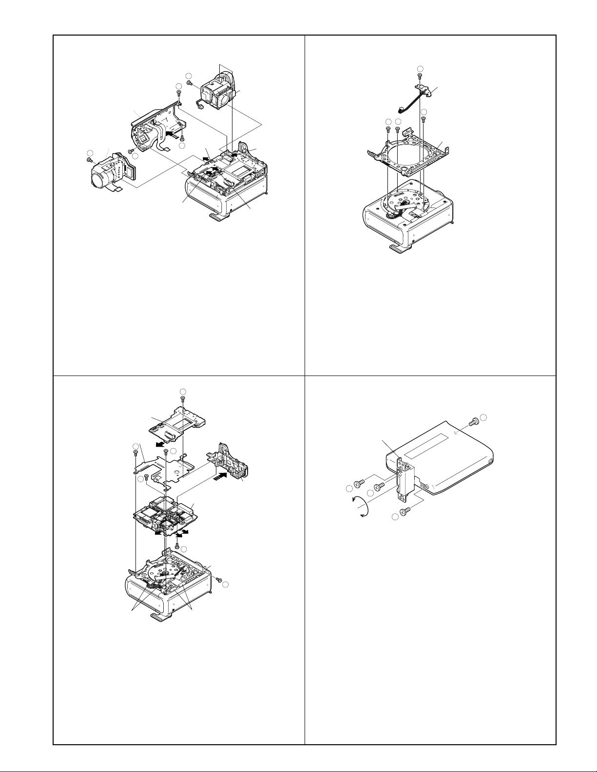
4. DISASSEMBLY OF THE SET
4-1. Procedure for disassembling the cabinet
Note:
Before removing the cabinet, turn OFF the power and make sure that the battery is not connected.
1.
· Remove the screw ((s) XiPSF14P06000).
· Remove the shoe cover by sliding it frontward, remove the screw
((f) XiPSF17P04000) and remove the shoe terminal cover.
· Remove the screw ((b) XiPSN17P03000).
· Open the LCD panel 90 degrees and remove the two screws ((x)LX-
HZ0050TAFN).
· Remove the two screws ((c)XiPSN17P04000) and remove the KS
camera front cover by pulling it frontward.
2.
· Disconnect the connector of the KS camera front cover.
· Disconnect the two LCD tilt FPCs of the liquid crystal panel.
· Remove the two screws ((r) XiPSN20P08000) and remove the LCD
panel.
· Remove the screw ((p) LX-HZ0063TAFN) and screw ((q)
XiPSN17P06000) that hold the camera L cabinet, open the terminal
cover and remove the three screws ((b) XiPSN17P03000).
Shoe cover
Shoe terminal cover
f
s
b
r
LCD panel
c
KS camera front cover
r
LCD panel
q
p
Camera L cabinet
x
x
c
b
3.
· Disconnect the hot shoe FPC of the hot shoe and remove the
camera L cabinet.
· Remove the screw ((c) XiPSN17P04000) and remove the KS
camera bottom cover.
· Disconnect the strobe FPC, remove the two screws ((a)
XiPSN17P02000) and remove the strobe unit.
å Precautions in servicing the strobe unit
Once put in the card mode, the main condenser of the strobe
unit stays still electrically charged. If touching the strobe unit or
its nearby parts, you may get an electric shock.
To avoid this, connect a 7 kΩ resistor (300-V withstand voltage)
across the main condenser for about 10 seconds. The condenser
will be discharged.
a
Strobe unit
b
LCD tilt FPC
KS camera front cover
Hot shoe FPC
a
Strobe FPC
Terminal cover
b
Connector
Camera L cabinet
KS camera bottom cover
c
8
Page 9
VL-Z7U/Z75U/Z8U
4.
b
x
Camera top cover
Camera unit
b
a
p
FPC(2)
Connector
· Remove the screw ((x) LX-HZ0050TAFN), screw ((p) LXHZ0063TAFN) and screw ((a) XiPSN17P02000), disconnect
the FPC (1) and remove the camera top cover.
· Remove the screw ((b) XiPSN17P03000) from the camera
unit, disconnect the FPC (2) and remove the camera unit.
· Remove the screw ((b) XiPSN17P03000), disconnect the
connector and FPC (3) and remove the VF.
VF
FPC(3)
FPC(1)
6.
b
Mechanism reversion detection PWB unit
u
u
u
PWB mounting angle
· Remove the screw ((b) XiPSN17P03000) and remove the
Mechanism reversion detection PWB unit.
· Remove the three screws ((u) LX-BZ0221TAFC) and remove
the PWB mounting angle.
5.
Sub PWB unit
Radiating angle
b
b
Connector
x
b
Terminal cabinet
Main PWB unit
x
PWB mounting angle
x
Tilt FPC
· Disconnect the two connectors of the sub PWB unit and main
PWB unit.
· Remove the two screws ((b) XiPSN17P03000) from the
radiating angle, remove the screw ((b) XiPSN17P03000)
from the PWB unit and remove each unit.
· Disconnect the two FFCs of the main PWB unit.
· Remove the two screws ((x) LX-HZ0050TAFN), remove the
screw ((x) LX-HZ0050TAFN) from the PWB mounting angle
and remove the terminal cabinet.
7.
b
LCD tilt unit assembly
b
a
b
· Turn the LCD tilt unit assembly 90 degrees.
· Remove the three screws ((b) XiPSN17P03000).
· Remove the screw ((a) XiPSN17P02000).
9
Page 10

VL-Z7U/Z75U/Z8U
4-2. Procedure for disassembling the cabinet
1.
· Remove the three screws ((e) XiPSF17P03000) remove the screw
((d) XiPSF17P02000) and remove the VCR bottom cover.
2.
· Remove the two screws ((e) XiPSF17P03000) and remove the tilt
cover.
· Remove the VCR front cover with the cassette cover opened.
· Disconnect the connector and two tilt FPCs, remove the three screws
((h) LX-BZ0220TAFC) and remove the KS camera tilt.
e
VCR bottom cover
e
e
d
e
e
Tilt cover
How to remove the VCR front cover
1. Remove the two couplings and turn the VCR front cover about 20 degrees in
the direction indicated by (1).
2. Turn the VCR front while sliding it in the direction indicated by (2) to disengage
the internal lug.
* If the VCR front cover is removed by turning it forcedly in the direction indicated
by (1), the internal lug may be damaged.
1
If the VCR front cover is removed
only by turning it in the direction
indicated
The internal lug
may be damaged
2
3.
· Remove the screw ((f) XiPSF17P04000) with the cassette lid opened,
disconnect the operation PWB FFC and remove the KS VCR operating
cover.
VCR front cover
h
h
KS VCR operating cover
h
KS camera unit
Tilt FPC
Connector
f
10
Operating PWB FFC
Page 11
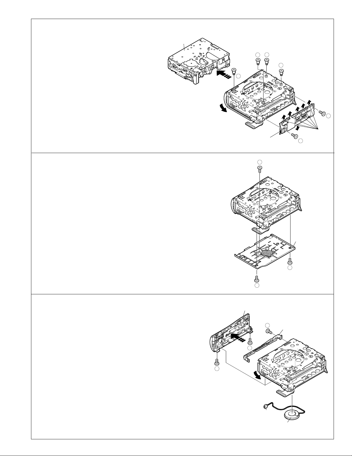
4.
k
a
a
w
w
w
Mechanism
Head amp PWB unit
FPC
· Disconnect the six FPCs of the head amp circuit board
unit.
· Remove the two screws ((a) XiPSN17P02000) and
remove the head amp PWB unit.
· Remove the three screws ((w) LX-BZA022WJFN) and
remove the screw ((k) LX-BZA023WJFD).
· Remove the mechanism with the cassette lid opened.
VL-Z7U/Z75U/Z8U
5.
· Remove the screw ((x) LX-HZ0050TAFN).
· Remove the two screws ((d) XiPSF17P02000) and remove the cassette
lid.
6.
· Remove the two screws ((d) XiPSF17P02000).
· Disconnect the connector of the speaker while removing the KS upper
lid cover with the cassette control lid opened.
· Remove the screw ((d) XiPSF17P02000) and remove the lock support
cover.
· Remove the speaker.
d
KS upper lid cover
d
x
Cassette lid
d
d
Lock support cover
11
d
Connector
Speaker
Page 12

VL-Z7U/Z75U/Z8U
5. MECHANISM ADJUSTING JIGS AND PARTS
5-1. Mechanism checking and adjusting jigs
<Note: Order of descriptions>
Sketch
1. Name
2. Part code
3. Code
* Model number and usage
1. Cassette torque
meter for PB
2. 9DASD-1015
3. DB
* 1mN·m/1.5mN·m
50 or more
ø2
No.0 Phillips bit
No.00 Phillips bit
1. Torque driver
150mN·m
2. JiGTD1500RTDH
3. CB
1. Torque gauge
2. JiGTG0045
3. CN
* For measurement of VS-
REW winding torque
1. Master plane
2. 9EQMP-VLPD1
3. CL
* For checking of
1. Torque gauge head
2. 9EQTGH-DH5000
3. BW
*
For torque gauge shown
left
1. Height adjustment jig
2. 9DAHG-PD1
3. BZ
* For height adjustment
height of reel table
1. Bit for hexagon nut
1. Alignment tape – (I)
2. VR3-GAZXS
3. CF
* Adjustment of running
system
(Linear signal)
1. Alignment tape – (II)
2. VR3-GTZQS
3. CG
* For adjustment of SW
point(Color bar signal)
*
90ADVC-TAPE available
with opposite side
distance of 3 mm
2. 95CM22001
3. BL
* For installation of Tu
guide nut
5-2. Parts for periodic inspection and maintenance
1. Oil
Cosmo Hydro HV22
2. 9EQ-OiL-HV22
3. AE
* Cosmo Oil Co., Ltd.
1. Cleaning paper
2. JiGDUSPER
3. AP
* DUSPER ∑ (SIGMA)
(Ozu Co., LTD.)
<How to make mechanism checking and adjusting jigs>
(1) Reel hub for back tension measurement (Fig.1)
1) Have the reel hub of a commercially available cassette
tape ready.(Disassemble the cassette tape and remove
the tape from the reel hub.)
2) Attach one end of a thread (having a length of about
20cm) to the reel hub using Scotch tape etc.
3)
Attach a weight of about 0.21N to the top face of the reel hub.
(2) Thread for pinch roller press force measurement
1) Have a commercially available thread having a length of
about 20cm ready.
1. Dry grease CFD-409Z
* Sankei Chemical Co., LTD.
1. Grease
Molykote YM-103
2. 99FGREASEYM103
* Dow Corning
2) Tie both ends together to loop the thread.
Thread
1. Tension gauge 4N
2. JiGSG0400
3. BK
* For measurement of
pinch roller press force
1. Driver for height
adjustment
2. 9EQDRiVER-DH5
3. BC
<Miscellaneous>
(1) Vernier calipers
(2) Precision screwdriver
(Phillips head and slot-
ted)
(3) Long-nose pliers
(with thin tips)
(4) Tweezers
<Note: Order of descriptions>
Weight
Fig. 1
1. Dial tension gauge
2. 9DAPTG-10-10W
3. CA
* PTG-10
* For adjustment of guide
roller
* Bit shape
1.4
3
1. Name
2. Part code
3. Code
* Model number and usage
1. Cleaning liquid
Industrial ethyl alcohol
* Commercial item
1. Loctite adhesive (1401B)
* Three Bond
1. Ultrathin cotton swab
* Commercial item
Reel hub
Fig. 2
(see figure below)
Tolerance ± 0.1
2
Tip thickness 0.5
Thread
12
Page 13
VL-Z7U/Z75U/Z8U
6. INSPECTION AND MAINTENANCE ITEMS AND INTERVALS
In order to maintain the quality of the mechanism section, perform the following maintenance and inspection. After repairing the
mechanism section, perform the following maintenance regardless of the number of hours of use by the user.
6-1. Maintenance and inspection list
Inspection and
maintenance location
Tape running section (See 8-3.)
Drum section, Video head
(See 8-3.)
Running system
Pinch roller
Capstan motor (Timing belt)
Swing arm
S reel table, Tu reel table
Center gear boss
Relay pulley shaft
Driving system
Loading motor
Mode SW
Abnormal noise
PB and VS/R winding torque
PB, VS/R and loading back tension
S reel table unloaded torque
Performance check
Number of hours of use (h)
500 1,000 1,500 2,000 3,000
<Rollers>
• Replace if abnormal rotation or swing (large) is found.
<Others>
• Cleans the portions that come in contact with the tape (the lower
drum helical portion in particular). Use the specified cleaning liquid.
• • • Replace. • • • Clean. • • • Lubricate. • • • Check.
Symptoms observed at the
time of maintenance
• Block noise
• Clogging of head
• Damage to tape
• Tape not running
• Tape sagged
• Block noise
• Abnormal noise
• Abnormal noise
• Ejecting cannot be made.
• Mode cannot be set.
• Tape not running
• Tape sagged
• Damage to tape
• Abnomaly in reproduced
picture
[Oil] Cosmo Hydro HV22
[Grease] Molykote YM-103
Sankei Chemical CFD-409Z
Notes and remarks
Note:
If no envelope output is obtained
in spite of the video head being
cleaned, replace the drum
component.
(If the envelope output is normal,
refer to "11. USEFUL TIPS".)
• Replace if any abnormal
condition is found.
• Apply oil.
[Oil]
Cosmo Hydro HV22
Note:
Apply oil to the shaft and
lightly wipe it off with a cloth.
• Replace if any abnormal
condition (noise etc.) is found.
• If a part is out of spec, replace
it.
[Loctite adhesive] Three Bond 1401B
[Cleaning liquid] Industrial ethyl alcohol
6-2. Cautions in handling the mechanism
(1)Cut washers removed at the time of part replacement etc. should be
replaced with new ones without fail.
(2) Because no volume adjustment is available in this mechanism, cleaning or
part replacement should be performed if the setting is not satisfied.
(3) About oil
a) Be sure to use the specified oil. (If any oil other than the specified oil is
used, various troubles will occur.)
b) When lubricating the bearing, be sure to oil free from foreign particles
such as dust. (If oil in which foreign particles such as dust are mixed is
used, it will cause wear and seizure to the bearing.)
c) The term "One drop of oil" here means the amount of oil on the point of
a needle etc. shown in Fig.1.
(4) Repairing of circuits, final adjustment of running system, etc. should be
performed with the cassette controller assembly installed in the mechanism.
(5) When operating the mechanism singly, apply voltage to the loading motor
to drive it. The voltage between the terminals should be 3 to 4V DC. (Do
not apply external voltage to the loading motor with the mechanism
connected with the main circuit board. Doing so could cause a failure.)
(Turning the gears forcedly by hand may cause them to get damaged.)
When placing the mechanism singly, use an appropriate spacer so that the
capstan motor is not rubbed.
(6) When installing the cassette controller, push the portion indicated by "A" in
Fig.2. Do not push other portions.
(7) Take care not to deform the components of the mechanism.
13
Oil
Ø1.5 or less
Fig. 1
Fig. 2
Page 14

VL-Z7U/Z75U/Z8U
7. ADJUSTING AND CHECKING OF MECHANISM
The items described here are relevant to the general on-site servicing (field service). This section does not cover adjustment and
replacement for which sophisticated equipment, jigs and techniques are required.
In order to maintain the initial characteristics of the mechanism, it is necessary to perform maintenance and inspection and also it is
essential not to damage the tape etc. In the case of an adjustment that requires a jig, be sure to use the specified jig.
<Caution>
(1) When adjusting and checking the mechanism, be sure to see that the power supply and the status are as indicated in
Caution on the title.
(2) Do not apply external voltage to the loading motor with the mechanism connected with the main circuit board. (Doing
so could cause a failure.)
(3) When running the tape, be sure to do so with the cassette controller assembly installed.
7-1. Checking of PB (REC) winding torque
AC adapter used, Cassette controller assembly installed
(1) Set the torque cassette with the cassette controller installed in the mechanism. In the SP record mode (or in the PB mode
if signals have been SP-recorded on the tape), check that the winding torque is within spec.
<Spec for PB (REC) winding torque>(If there is a torque ripple, read the center value.)
0.7+0.2/-0.05N·m, Ripple: 0.1mN·m or less
7-2. Checking of VS-REW winding torque
AC adapter used, Cassette controller assembly not installed (Mechanism only)
(1) Remove the cassette controller, turn ON the down SW while referring to 9-3, operate
in the test mode (T01) and select the VS-REW mode.
(2) Set the torque gauge in the S reel table, push the tip of the tension pole with your finger
in the direction shown by Arrow A to release the tension band, and check that the
winding torque is within spec. (Fig.1) (Do not apply the own weight of the torque
gauge or rotate it during measurement.)
<Spec for VS-REW winding torque>
(If there is a torque ripple, read the center value.)
1.5 ± 0.15N·m, Ripple: 0.15mN·m or less
(3) After checking the winding torque, remove the torque gauge and turn OFF the down
SW. The mechanism will automatically go into the standby mode.
Fig.1 How to release the tension
band when measuring the
VS-REW winding torque
7-3. Checking of height of reel table
3 to 4V DC, Cassette controller assembly not installed (Mechanism only)
(1) Remove the cassette controller. (Refer to 9-2.)
(2) Apply 3 to 4V DC to the loading motor while referring to 9-1 and select the
PB mode.
(3) Fit the holes of the master plane to the two guides (portions A and B) shown
in the Fig.2, taking great care not to allow master plane to strike the running
parts such as the drum and guide roller or the MIC contact.
(4) Using a pair of vernier calipers etc., measure the heights of the reel-supporting
faces of the S reel table and Tu reel table from the top face of the master plane
and check that the measured heights satisfy the set values. (Fig.3)
When measuring the height of the S reel table, push the tip of the tension
pole with your finger in the direction shown by Arrow A to release the tension
band. (Fig.1)
(5) If the measured height does not satisfy the set value, replace the reel table
and make checking again.
<Note> After replacement, select the L start mode (see 9-1) and check that the
reel table rotates smoothly.
Reel-supporting face
2.4±0.1
Set value of height
of reel table
(3)
Fig.3
A
MIC contact
Fig.2 Checking of reel table
2.4±0.1
Set value of height
of reel table
B
14
Page 15

VL-Z7U/Z75U/Z8U
7-4. Checking and adjusting of tension pole position during
REC (PB)
3 to 4V DC, Cassette controller assembly not installed (Mechanism only)
(1) Checking
Check that the tension pole is located in the prescribed position as shown in Fig.4
at the start of a 60-minute tape.
If the tension pole is not located in the prescribed position, take out the tape and
make adjustment according to the procedure shown below.
(2) Adjusting (See Fig.4.)
1. Select the PB mode without setting a tape.
2. Slightly loosen the screw 1 (to such an extent that the T band adjustment base
2 can be moved.)
3. If the tension pole is dislocated inward from the prescribed position, shift the
T band adjustment base 2 in the direction shown by Arrow (A). If it is dislocated
outward from the prescribed position, shift the T band adjustment base 2 in the
direction shown by Arrow (B). Then fix the T band adjustment base 2 with the
screw 1.
(For how much the T band adjustment base is to be shifted, refer to Fig.4.)
4. Check the tension pole position as described in "(1) Checking" above.
5. If out of position, make readjustment.
7-5. Checking and adjusting of REC (PB) back tension
torque
AC adapter used, Cassette controller assembly installed
(1) Checking
Set the torque cassette (SD-1015). In the SP record mode (or in the PB mode if
signals have been SP-recorded on the tape), check that the feed-side torque is
within the following spec.
<Spec>(If there is a torque ripple, read the center value.)
0.55 ± 0.05N·m
(2) Adjusting (See Fig.5.)
If the measured back tension torque is out of spec, make adjustment according
to the following procedure.
1. Slightly loosen the screw 3.
2. If the back tension is higher, shift the T-SPR adjustment ANG in the direction
shown by Arrow (D). If it is lower, shift the T-SPR adjustment ANG in the
direction shown by Arrow (C).
3. After adjusting the back tension torque, fix the T-SPR adjustment ANG with the
screw 3. Apply loctite adhesive to screw 3.
<Reference>
Screw tightening torque: 0.04 N·m
Apply loctite
adhesive.
Tension pole position
(Based on drum base outside shape)
0±0.3
Fig.4 Adjusting of position (tape exists)
Fig.5 Checking (tape exists)
Drum base
T pole
T band adjustment
base 2
Screw 1
Screw 3
T-SPR adjustment ANG4
7-6. Checking of S reel table unloaded torque
3 to 4V DC, Cassette controller assembly not installed (Mechanism only)
(1) Remove the cassette controller assembly, apply 3 to 4V DC to the loading motor
and select the L start mode. (See 9-1.)
(2) Move the swing arm to the Tu reel table side. At this time, take care not to damage
the gears etc. (See Fig.6.)
(3) Set the reel hub for back tension measurement on the S reel table.
(4) Using the dial tension gauge, pull the thread of the reel hub in the direction shown
by Arrow A and check that the tension is within spec.
<Spec>
(If the tension fluctuates, read the center value.)
10mN or less
Fig.6 How to measure the S reel table unloaded torque
15
Move the swing arm to
A
the Tu reel table side.
Page 16

VL-Z7U/Z75U/Z8U
7-7. Checking of loading back tension
3 to 4V DC, Cassette controller assembly not installed (Mechanism only)
(1) Apply 3 to 4V DC to the loading motor and select the L start mode. (See 9-1.)
(2) Move the swing arm to the S reel table side. At this time, take care not to damage
the gears etc. (See Fig.7.)
(3) Set the reel hub for back tension measurement on the Tu reel table.
(4) Using the dial tension gauge, pull the thread of the reel hub in the direction shown
by Arrow A and check that the tension is within spec.
<Spec>
(If the tension fluctuates, read the center value.)
27.5 ± 7.5mN
7-8. Checking of VS-REW back tension
3 to 4V DC, Cassette controller assembly not installed (Mechanism only)
(1) Apply 3 to 4V DC to the loading motor and select the VS-REW mode. (See 9-1.)
(2) Move the swing arm to the S reel table side. At this time, take care not to damage
the gears etc.
(3) Set the torque gauge in the Tu reel table.
(4) While turning the torque gauge counterclockwise (one turn in three seconds),
check that the torque is within spec.
<Spec>
(If the tension fluctuates, read the center value.)
0.8+0.2/-0.05mN·m
Move the swing arm
to the S reel table
side.
Fig.7 How to measure the loading back tension
A
7-9. Checking of pinch roller press force
3V DC, Cassette controller assembly not installed (Mechanism only)
(1) Hook the thread for pinch roller press force measurement over the pinch lever (position A in Fig.8).
(2) Put the mechanism into the PB mode to press the pinch roller against the capstan shaft.
(3) Hook the thread for pinch roller press force measurement over the tension gauge and pull the tension gauge in the direction shown
by Arrow B in Fig.10 so that the pinch roller is slightly separated from the capstan shaft.
(4) Return the pinch roller gradually and read the value indicated when the pinch roller comes in parallel contact with the capstan shaft
(see Fig.9). Check that the read value is within the following spec.
<Spec>
1.8+0.4/-0.4N
<Note> After measuring the press force of the pinch roller, promptly exit from the PB mode to separate the pinch roller from the capstan
shaft. (If the pinch roller is left pressed against the capstan shaft for a long time, the pinch roller will be deformed.)
Capstan shaft
Pinch roller
B
Fig.8
A
OK
Fig.9
NG
16
Right guide
Fig.10
Page 17

VL-Z7U/Z75U/Z8U
8. ADJUSTMENT OF RUNNING SYSTEM
8-1. Outline of adjustment of running system
(Replacement parts)
· Tu guide and arm
· Slide chassis
(Replacement parts other
than above)
· Pole base
· Guide roller
· Drum assembly
· Cap motor, etc.
8-2. Adjustment of height of running system
· After replacement of the Tu guide and slide chassis, adjust the height of the Tu guide using the height adjustment jig.
· If wrinkles are found in the tape, turn the Tu guide to remove them.
(For further details, refer to "Coarse adjustment of running system".)
· After adjusting the Tu guide height, apply screw loctite at the tip of the shaft.
Readjustment of height
Presetting of height not
necessary
Tu guide
Installation of
cassette controller
View A
Preparations for
adjustment of
Running system
Adjusting
procedure(8-3)
Height
adjustment jig
Coarse adjustment
of Running system
Adjusting
procedure(8-4)
Final adjustment
of Running system
Adjusting
procedure(8-5)
Bottom edge
Apply it in this direction.
Master plane
Height
adjustment jig
View A
Align the top face of the lower flange of the Tu
guide with the bottom edge of the height
adjustment jig.
After adjusting the height, turn the head
clockwise 180 degrees.
Master plane
8-3. Preparations for adjustment of running system
Measuring instrument and Jig : Oscilloscope, Adjustment remote control, Height adjustment screwdriver, Alignment tapes (for
adjustment of running system and adjustment of SW point), Master plane, Height adjustment jig
<Method and description>
(1) Clean the surfaces that come in contact with the tape. (Clean
well the drum surface and the lower drum helical surface in
particular.)
(2) Install the cassette controller.
(3) Connect the oscilloscope to each TP of the joint circuit board.
(4) Turn ON the power of the AC adapter.
(5) Select TEST mode T-05 with the adjustment remote control.
(6) Play back the alignment tape for running system adjustment
and check that the tape is moving in the SP mode.
(7) While observing the PB envelope on the oscilloscope, adjust
the running system so that the envelope becomes flat in
states of [+1/4 shift] and [-1/4 shift].
(Each time the PB key is pressed, the shift amount changes
as shown below.)
+1/4 shift - Normal - -1/4 shift - Normal
S guide
Tension pole
Sup guide roller
Drum
Tu guide roller
Tu guide
Capstan shaft
Pinch roller
Reel
17
Page 18

VL-Z7U/Z75U/Z8U
8-4. Coarse adjustment of running system
(Cassette controller installed)
1. Adjustment of height of Su and Tu guide rollers
<Method and description>
(1)Play back the alignment tape for running system
adjustment and make adjustment so that the inlet
and outlet sides of the envelope become flat.
(2)In states of [+1/4 shift] and [-1/4 shift], make
adjustment in the same manner as described in (1)
above.
2. Checking of V/SR envelope waveform
<Method and description>
(1) In the V/SR mode, check that the envelope waveform
is shaped uniformly.
(2) If the envelope waveform is not shaped uniformly,
fine-adjust the guide roller and Tu guide.
NG
±1/4 shift
Inlet side Outlet side
Normal
A
Make adjustment so that A B.
B
NG
±1/4 shift
3. Checking for wrinkles in tape
<Method and description>
(1) In the PB mode and V/SR mode, check the tape for
distortion between the Tu guide and the pinch roller.
- If wrinkles are found, make adjustment within a
range of ±180 degrees.
Pinch roller
Wrinkle
Tu guide
Distortion
Distortion
- After making adjustment, apply loctite adhesive to
the tip of the shaft.
4. Checking of envelope waveform rise time
<Method and description>
(1) Check the envelope waveform rise time in switching from the V/SR mode to the PB mode. - 5 seconds or less
(2) Check the envelope waveform rise time in switching from the STOP mode to the PB mode. - 5 seconds or less
8-5. Final adjustment of running system
(Cassette controller installed)
1. Adjustment of height of Sup and Tu guide rollers
<Method and description>
(1) If the ratio of MIN to MAN of the envelope waveform is less
than 60%, adjust the height of the guide roller again. (See
Fig.1.)
(2) Perform unloading and then loading again, select the PB
mode and check that there are no significant changes in
the envelope waveform.
Fig.1
2. Adjustment of PB SWP
<Method and description>
(1) Play back the alignment tape for SW point adjustment.
(2) Using the adjustment remote control, make SWP automatic adjustment.
(3) Check that an OK is given as a result of self-judgment. In the case of a NG, adjust the GR height again.
* After replacement of the mechanism and drum, adjust the phase and equalizer using the adjustment remote control.
(Refer to "10. ADJUSTING THE ELECTRICAL CIRCUITS".)
18
Page 19

VL-Z7U/Z75U/Z8U
9. ASSEMBLING OF MECHANISM SECTION AND PART REPLACEMENT
(DISASSEMBLING AND ASSEMBLING)
This section describes the method of assembling the mechanism section and the method of part replacement.
For how to remove the cabinet etc., refer to " 4. DISASSEMBLY OF THE SET".
<Cautions>
1. Cut washers removed at the time of part replacement etc. should be replaced with new ones without fail.
2. When assembling the mechanism, take care to prevent screws, washers and foreign matter from getting into it. If such things
get into the mechanism, it will cause the mechanism to malfunction.
3. Be sure to use the specified cleaning liquid, oil, grease and loctite adhesive shown below. Failure to do so will cause the
mechanism to malfunction.
Oil: Cosmo Hydro HV22 (Cosmo Oil) Loctite adhesive: 1401B (Three Bond)
Grease: Molykote YM-103 (Dow Corning), Suncall CFD-409Z (Sankei Chemical Co., LTD.)
Cleaning liquid: Industrial ethyl alcohol
9-1. Mechanism mode
To operate the mechanism singly, apply 3 to 4V DC to the loading motor.
(Do not apply external voltage to the loading motor with the mechanism connected with the main circuit board. Doing so could cause a failure.)
(1) Ejection mode
This mode is used to take out a cassette. In this mode, the
ejection lever is shifted farthest in the direction shown by
Arrow A. (In this mode, the cassette controller assembly
cannot be locked.)
(2) Standby mode
This mode is used to set a cassette. In this mode, the slide
chassis is farthest away from the drum and the ejection lever
is turned (the cassette controller assembly can be locked).
(The tip of the ejection lever is hidden behind the main chassis
and the moving part of the down SW is visible.)
Ejection lever
A
Back view
Main chassis
EJECTION MODE
(3) L start mode
This mode is used for the Tu reel hub to take up the tape
of a cassette whose leader tape is visible. (In this
mode, the S main brake is located away from the S reel
table.)
Down SW
(moving part)
Ejection lever
Main chassis
STANDBY MODE
(4) Stop mode
This mode is used for stopping (camera mode:
RecLock). In this mode, the S and T pole bases are
pressed against the drum base and the S main brake
is engaged with the S reel table. However the pinch
roller and capstan shaft are separated.
S pole base
Drum base
T pole base
Capstan shaft
Back view
Pinch roller
S reel table
S main brake
L START MODE
S reel table
S main brake
STOP MODE
19
Page 20

VL-Z7U/Z75U/Z8U
(5)PB (Record, Fast forward, Fast rewind, VSF and VSR)
mode
This mode is used for playback, recording, fast-forwarding,
fast -rewinding, VSF and VSR. In this mode, the pinch roller
is pressed against the capstan shaft and the S main brake
is located away from the S reel table.
Capstan shaft
Pinch roller
S reel table
S main brake
PB (RECORD, FAST FORWARD,
FAST REWIND, VSF AND VSR) MODE
9-2. Cassette controller assembly
<Procedure for removing the cassette controller> (The cassette controller can be installed and removed without removing the cover.)
(1) Apply 3 to 4V DC to the loading motor to establish the standby mode. When removing the cover from the cassette controller, remove
the tow screws (A). (See Fig.1.)
(2) Push the lock lever in the direction shown by the arrow and move up the cassette controller. (See Fig.2.)
(3) Remove the two screws (C) and remove the down guide (D) in the direction shown by the arrow (E). (See Fig.3 and Fig.4.)
(4) Shift the cassette controller in the direction shown by the arrow (F), remove the inner arm guide shaft L and the groove of the inner
arm R toward the inside of the mechanism, and turn the cassette controller. (See Fig.5 and Fig.6.)
(5) Turn the cassette controller in the direction shown by the arrow (H) and shift it in the direction shown by the arrow (I) to remove it
from the slide chassis. (See Fig.7.)
(A)
At this position, remove the inner arm guide
shaft L toward the inside of the mechanism.
Fig.1 Fig.2
(C)
(C)
(D)Down guide
E
Fig.3
(F)
Fig.5 Fig.6
E
Fig.4
(F)
(B)
At this position, remove the groove of the inner arm
R toward the inside of the mechanism.
20
Page 21

VL-Z7U/Z75U/Z8U
H
II
Fig.7
H
Fig.8
9-3. Method of operating on the circuit board with the cassette controller assembly removed
If this method is performed improperly, the tape may be damaged. Therefore do not use this method except in special cases
such as measuring the VSR torque. Be sure to follow the cautions shown in this manual.
(1) Apply 3 to 4V DC to the loading motor to establish the standby mode.
(2 Insert a sheet of thick paper folded in two as shown in Fig.9 into the position shown in Fig.10 to turn OFF the down SW.
(Pass the paper along the heavy line in the figure.)
Note) To go into the REC mode, press the pin of the recognition SW.
(3 Selecting the test mode (T-01) with the adjustment remote control without setting a tape will make it possible to operate
the mechanism with the mode keys.
(4) For ejecting, remove the paper inserted in step (2) above.
Pass the folded paper between
the slide chassis and the lock cam
to press the moving part of the
down SW.
34~36
5
Fold a sheet of paper
in two.
Fig.9
Recognition SW pin
Fig.10
Press
Moving part of
down SW
21
Page 22

VL-Z7U/Z75U/Z8U
9-4. Phase-adjust
Phase-adjust the following parts.
(1) Mode SW
(2) Main cam
(3) Sub cam (The main cam and sub cam should be also phase-adjusted for the chassis.)
(4) S loading arm
(5) Tu loading arm
(6) Loading drive gear (main cam, sub cam, S loading gear)
Note) Check the marker position carefully before disassembling.
Note) When installing the loading drive gear, check that the main cam, sub cam, S loading gear are all phase-adjusted.
(5)Tu loading arm ass'y(4)S Loading arm ass'y
(1)Mode SW
Phase adjustment
Phase adjustment
mark
hole (for chassis)
(3)Sub cam
Phase adjustment
(gear section)
Phase adjustment
hole (for chassis)
(2)Main cam
Phase adjustment
mark
(4)S loading arm ass'y
Phase adjustment
mark
Phase adjustment hole
(for chassis)
(6)Loading gear drive gear
Fig.1
(5)Tu loading arm ass'y
Fig.2
22
Page 23

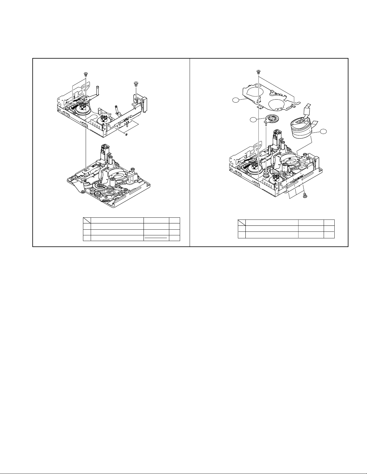
9-5. Assembling method
9-5-1. Method of assembling the main chassis assembly
Note) For reference, numbers are prefixed to parts names to show the sequence of assembly.
(For the greasing/oiling and cleaning locations, refer to the diagram of greasing/oiling locations.)
VL-Z7U/Z75U/Z8U
1.
2.
302
(1)Mode SW
304
(3)Main cam
(4)T arm operating lever
(3)S brake operating
lever
308
307
(2)SL drive lever
A
303
(2)LM/Mode FPC
305
(4)Ejection lever
Type
Tightening torque
A M1.4xL1.6(Special screw) 0.4mN·m2
H
309
B
306
(1)Sub cam
Q'ty
4.
5.
321
(4)S pole base loading
arm ass'y
322
(6)S Loading gear
324
(2)Loading drive
gear
E
(1)T pole base loading arm
(5)S press SPR
323
ass'y
320
319
(3)Tu loading
gear
Type
318
(2)Tu press SPR
D
(7)S loading arm
sub ass'y
Phase adjustment
Tightening torque
D S Tight M1.4xL3.0 0.4mN·m3
E M1.4xL2.0
B
(t0.2 special screw)
G
F
325
(1)Guide rail
0.4mN·m1
Q'ty
In alignment with
chassis hole
BCWø1.2-ø3.0t-0.25 1
Type
Tightening torque
Q'ty
Phase adjustment (back)
HCWø0.7-ø1.8-t0.2 1
In alignment with
3.
C
B
316
(7)Relay pulley
314
(1)SLA support
310
C
Type
(4)TLA support
(3)DEW sensor
312
311
(2)L Motor ass'y
D
(5)Center gear
C
315
(7)Capstan motor
ass'y
313
(6)CAP FPC protection tape
Tightening torque
6.
Q'ty
chassis hole
(1)Pinch press
lever ass'y
(2)Pinch press SPR
C S Tight M1.4xL2.0 0.4mN·m5
D S Tight M1.4xL3.0 0.4mN·m1
BCWø1.2-ø3.0t-0.25 1
Phase adjustment (front)
F M1.4xL1.5
Type
(t0.2 special screw)
Tightening torque
Q'ty
0.4mN·m1
G M1.2xL4.6 0.4mN·m1
(t0.2 particularly special screw)
BCWø1.2-ø3.0t-0.25 1
326
327
329
(3)Pinch lever
ass'y
Type
H
328
(4)Pinch lever return SPR
Tightening torque
HCWø0.7-ø1.8-t0.2 1
Q'ty
23
Page 24

VL-Z7U/Z75U/Z8U
9-5-2. Method of assembling the slide chassis assembly
1.
3.
(2)T-SPR adjustment
ANG
343
I
(19)T arm SPR
(8)Guide nut
349
(6)Tu guide flange
347
(7)Tu guide
Type
348
(6)Tu guide flange
347
(5)Guide adjustment SPR
346
(4)Tu guide arm
ass'y
345
344
Tightening torque
I
(1)Slide adjustment
ANG
342
(3)Tu guide arm SPR
I Precision type 2·M1.4xL1.0 0.4mN·m2
359
357
C
(17)Tension arm ass'y
Q'ty
2.
(15)S main brake
355
(13)S reel table ass'y
(16)S brake SPR
356
(14)Tu reel table ass'y
353
354
(11)T main brake
352
351
(10)T brake gear
350
(9)VSR brake lever
(18)Tension band ass'y
358
H
Type
Tightening torque
Q'ty
C S Tight M1.4xL2.0 0.4mN·m1
(Tightening fully)
0.05mN·m
(Tightening temporarily)
HCWø0.7-ø1.8-t0.2 1
24
Page 25
VL-Z7U/Z75U/Z8U
377
(22)Drum ass'y
371
(20)Swing arm ass'y
372
(21)Reel cover ass'y
D
I
9-5-3. Method of combining the main chassis assembly and the slide chassis assembly
(1) Position the assemblies as shown in the figure below (the pole base is slightly protruded).
(2) Insert the operation pins (tension arm, Tu guide arm) of the slide chassis assembly into the locations of the main chassis assembly
shown in the figure below, fit the SL drive lever pin of the main chassis assembly into the groove of the slide chassis (the groove
of the slide adjustment ANG), and then fix with the two screws.
1.
C
D
J
Type
C S Tight M1.4xL2.0 0.4mN·m2
D S Tight M1.4xL3.0 0.4mN·m1
JWø2.1-ø4-t0.25 2
Tightening torque
Q'ty
2.
Type
D S Tight M1.4xL3.0 0.4mN·m1
I Precision type 2·M1.4xL1.0 0.4mN·m2
Tightening torque
Q'ty
25
Page 26

VL-Z7U/Z75U/Z8U
9-5-4. Diagram of greasing/oiling locations
26
Page 27

9-6. Method of installing the cassette controller
(2)Completed cassette
controller
1
VL-Z7U/Z75U/Z8U
2
3
Left side view Right side view
Left side view
B-1 B-2
Left side view Right side view
(3)Down guide
(1)Main slide
ass'y
A-1
A-2
Right side view
B-1、2
4
Mechanism viewed from above
A Ml1.4xL2.0(Precision type 2) 0.4mN·m2
Type
B M1.7x2.5(Precision type 2) 2
Tightening torque
Q'ty
(4)Cassette cover
Right side view
5
Right side view
C: Move down the cassette controller by pushing this
portion. When the cassette controller is locked,
attach the cassette cover.
27
Page 28

VL-Z7U/Z75U/Z8U
9-7. Method of taking out the cassette with the mechanism operating singly
(1) Apply 3 to 4V DC to the loading motor for slight unloading.
(2) If the tape is slack, turn the rotor (mechanism backside) of the capstan motor by hand to take up the slack in the tape.
(3) Repeat steps (1) and (2) above. When the pole base is completely unloaded, check that the tape is not slack.
(4) Then apply 3 to 4V DC to the loading motor again. The cassette controller will move up.
(5) Take out the cassette.
Note) When applying 3 to 4V DC to the loading motor for unloading, do so as shown in Fig.1.
Direction of rotation of the rotor
of the capstan motor (from
mechanism backside)
Loading motor
pole
+○
pole
−○
Fig.1
28
Page 29

VL-Z7U/Z75U/Z8U
10. METHOD OF ADJUSTING THE ELECTRIC CIRCUIT
-Before making adjustment-
· It seems that, in most cases, this adjusting method is used when it becomes necessary to adjust the electric circuit as a result of
replacement of worn mechanism parts or the video head. When adjusting the electric circuit, check that the mechanism operates
properly (the mechanism is adjusted completely). If a failure occurs in the electric circuit, be sure to locate the fault using a
measuring instrument and then perform repairing, replacement and adjustment, as described in this adjusting method.
Avoid performing undue adjustments etc. without using proper measuring instruments.
· The electric circuit components in the circuit board unit of this product are densely-packed into packages. Most of them are surfacemounted for downsizing.
When replacing components in servicing the product, perform replacement work swiftly with a soldering iron.
In general, surface-mounted components are inferior in heat resistance to large-sized discrete components used in TV sets,
stationary decks, etc. Heating the electrode of a surface-mounted component with a soldering iron for a long time needlessly will
therefore lead to a failure. Take great care not to do so.
Take special care in this respect when replacing chip multilayer capacitors in particular.
We recommend you to use a ceramic soldering iron (Tip temperature: 250°C, Contact time: 5 seconds or less).
10-1. Adjustment of liquid crystal video section
List of measuring jigs
・ColormonitorTV
・Digitalvoltmeter
・DCpowersource
・Audiogenerator
(CRoscillator)
・Frequencycounter
・ACadapter
・StereoAVoutputcable(supplied)
・Adjustmentremotecontrol
(RRMCG0033TASA)
・Signalgenerator
(NTSCpatterngeneratorLCG-401/
401YC:ManufacturedbyLeader)
・Oscilloscope
・Vectorscope
・Tapeforrecording
・DCcable(suppliedwithACadapter)
・Extensionwireofvideosection
・Alignmenttape
・
Errorrateadjustmenttape(referencetape)
90ADDVC-TAPE(colorbar)
RTPEVA001WJZZ
VL-Z7U/Z75U/Z8U
No. Connection section Connector REF. No.
Specifications of service jigs
No. of pins
New/
Parts cord
Cont. code
1 H/A PWB — MAIN PWB1 SC307—SC3302 33P N QCNW-B315WJZZ AN
2 H/A PWB — MAIN PWB2 SC308—SC3301 33P N QCNW-B315WJZZ AN
4 MAIN — LITHIUM PWB SC8800—SC5800 27P-25P QPWBHB742WJZZ Product FPC used AE
5 MAIN — RUNTA005WJZZ SC1201 80P C QCNW-1373TAZZ BQ
6 RUNTA005WJZZ — SUB P2901 80P N RUNTZA005WJZZ AX
7 Hot shoe — SUB —SC501 15P QPWBHB739WJZZ Product FPC used AH
8 Menu key — SUB SC2002—SC501 9P-15P QPWBHB739WJZZ Product FPC used AH
9 H/A PWB — MAIN PWB P301—P3301 5P QCNW-B171WJZZ Product wire used AF
10
TP jig for envelope checking
11 Power supply SC310—SC2101 12P QCNW-B167WJZZ Product FFC used AC
12 ZOOM SC311—SC2201 10P C QCNW-1769TAZZ BF
13 CCD PWB — MAIN SC1001—SC1202 33P QPWBHB738WJZZ Product FPC used AD
14 Lens unit — SUB SC551 25P CLNS-A005RMA5 Product unit used BQ
15 MIC — SUB P3602 4P RMiCC0108TAZZ Product unit used AP
16 FLASH — MAIN —SC1204 12P QPWBHB740WJZZ Product FFC used AD
17 MECHA TURN — MAIN P1201 2P DUNTKB732PM00 Product unit used AG
19 SPEAKER — ZOOM P2201 2P VSP0020P-B2WN Product unit used AK
20 LCD UNIT — MAIN SC1800/SC1801 18Px2 QPWBHB736WJZZ Product FPC used AR
P3303 30B-B N RUNTZA004WJZZ AW
Price
29
Page 30
VL-Z7U/Z75U/Z8U
Lens
CCD PWB
QPWBHB738WJZZ
HEAD AMP PWB
SC303
SC307
SC301 SC308
SC304
SC310
SC306
SC311
SC305
P301
10
10
7
27
QCNW-B171WJZZ
LCD
LAMP
FLASH
ZOOM PWB
P2201
SC2201
SPEAKER
HOT Shoe
SC2002
MENU
SC5800
SC5801
USB
BAT
P900
SC1501
SD
SC501
J600
J7401
J1401
J2900
P3602
SUB PWB
P2901
SC1201
W8089
P3303
SC3302
SC3301
P1201
P3301
SC1801
SC1800
SC1204
MAIN PWB
SC8800
VF_IF
VF_IF
P8800
RMiCC0108WJZZ
POWER SW
QMPWCB734WJZZ
SC802
LCD PWB
SC801 SC800
SC803
SC9800
18 18
15
25
3
22
25
9
80
4
SC551
80
12
1818
30
2
27
SC1202
33
33
33
33
33
12
2
5
MECHA TURN
24
6
10
SC2101
12
10
10
2
21
*1
*2
QPWBHB740WJZZ
QCNW-1373TAZZ
RUNTXA005WJZZ
RUNTZA004WJZZ
SC1001
5
AV
DV
HP
DC
QPWBHB742WJZZ
QPWBHB739WJZZ
QCNW-B315WJZZ
QCNW-B315WJZZ
QCNW-B167WJZZ
QCNW-1769TAZZ
LI
13
14
9
17
20
16
19
4
7
8
15
1
2
10
5
6
11
12
QPWBHB736WJZZ
Mechanism
*1: Under surface contact
*2: Top surface contact
Caution: Don't make a mistake in putting in SC3301 and SC3302.
HOLE SENSOR
VL-Z7U/Z75U/Z8U Service jig configuration
30
Page 31

[TEST POINT]
TL7824(VF_G_OUT)
VF_DAC full scale
TL6807(G_OUT)
DAC full scale
2
TL1431
R717 R728 C713
C711
R743
R714
TL701
TL3303
R744
C731
R709
R702
C703
R742
R712 C716
R723
R705
R724
R732
P3301
C1809
R1824
R1823
C1810
SC1800
C1439
C1438R1442
(Wiring board diagram: Main Side A)
TL3304
TL3302
SC3301
TL3310
X702
R756 R760 R764
R761 R765 R766
R745 R722 R762
C719
R746
R748
C720
C709
IC706
R754
C728
R751 R753 C726
C725 R752 C723
C737
R750
R757
C730
IC701
R707 R715 C735
R729
R759
C710
R741
C733
C708
R736
R737
R763
R738
Q704
R1802
R718
R1801
R771
Q705
C1802
R1805
R772
C704
R1800
R1818
R747
R1422
R1402
R1419
Q1402
C1406
C1407
R1406
C1416
R1405
C1402
IC1401
C1410
C1441 L1404
C1408
IC1431
L1431
Q1431 L1802
C1431
R1437
C1435
R1436 C1801
Q1433
C1434R1432
R1434
R1433
R1435
R755
R758
Q1800
R1803
R1804
R1806
R1413
C1418
C1409
C1437
R1440
R1441
C1440
C1432
R1431
Q1432
C1433
Q1802
R735
R725
R720
C1805
R1814
R1813
Q1801
R1817
R1808C1803
C1806
R1820
C1804
R1811
R1807
R1810
R1816
R1819
C1800
C1411
C1412
R1414
Q1403
Q1404
R1423
R6802
R1462
R1461
R1424
R6816
R6817
R6803
Q1405
C6800
R6805
TL6804
TL6803
C1419
R1421
Q6801
R6806
R1404
C6802
R6804
R6813
C6801
C6807
R6810
R6800R1403C1417
R6807
R6812
R1439
C6804
R1438
R6809
Q1434
C1436
C4481
L4406
R4489
Q4483
L4404
Q4481
R4471
C4404
C4483 R1809
R4472
SC3302
TL913
R3321
C3321
R3320
C3320
C724R1932
Q703
R768
R749
C712
R779
R716
C722
R703
R704
R713
C707
R721
Q701 Q702
R734 R731 C729 R719
R711
C732
R782
C727
R730
R726
R727
C715
R708
R710
R706
X701
TL8803
C705
R1815
R1812
C1815
R1827
Q1803
R4402
R4401
C4402
C4401 L1800
C4405
IC6801
C6814
TL6807
R6819C6815
C6813
R6820R6818
C6816 FB4405
TL6809
TL7819
C6811
C6812
TL6801
TL6802
R6808
R6811
D6800
L6800
C6805
C4406
C4416
C4419R4494C6806 C6810
R4485
C4420
C4485
Q4482
C4409
R4486
C4407
C4482
R4488
R4487
IC704
C714
IC703
C7802
C7800
L7800
C4408
R4404
Q3320
L701
R701
C7806
C7804
TL7824
R7828R7831
IC4401
C4421
C4410
R932
C706
D701 C3716
R739
C734
R780 C702
L3405
C701
L3404
C1911
R1925
R1928
L8800
C8805 L8801
C8800
C7825
R7830
IC7802
R7827
C7803 Q1913
R7826
R7829
R4436
R4437
C4413
Q4432
R4435
VL-Z7U/Z75U/Z8U
Q908
C980
C955
C960
Q909 C953
L908
C939
FB3701
C3713
C3707
L918
L915
R982
C938
C1901
C3705
C3712
IC3701
R3709
R3712
R3708
R3738
R8842
Q3701
C982
TL902
C981
Q1991
R1991
TL901
L900
R1992
R1990
Q1990
C931
C930
C1990
Q903
Q900
C932 R970
TL8801(VF_COM)
VF_COM
L901
C934
Q1901
TL910
C3708
TL908
Q1905
R1941
TL8804(VF_VG)
VF_WB
FB8800
C1904
TL8805
TL8804
C3702 L3702
TL8806
C3709
R3710
R3718R3739
R8836
TL3701
R8834
R8835
C3701 L3701 L903 C933 L902 C936
C3703
R3737
C3711
C3706
TL3702
R3740
TL8805(VF_VR)
VF_WB
TL8806(VF_VB)
VF_WB
L917
C974
Q911
L923
C992
C991
R951
C3436
C3473
C978
Q1912
TL903
D960
R1926
R1924
TL904
R1927
Q8800
C8804
R8800
IC8800
C7805R8802 R8801
C4427
C7808
C7809
C7807
R4403
C7801
TL4439
TL4438
C4422C4414
C4436C4415
C4435
L916
C973
Q907
C975
L911
C990
C956
C962
D916
C929
R8804
C8801
C4403
C6803
L7810
R7811
C7810
R7812
R7800
C4428
R4415
C4418
C4417
R4495
TL4440
C4426
R4414
R4454
R4456
C4454 R7820R7832
X4451
R4451
C4451
C4462
C4424
C4423
R4462
R4461
R4460
C4465
C4463
Q906
R990
C972
R987 C970
R988 C971
Q904
C954
Q910
R983
L931
Q905
TL8801
C8806
R8805
Q8801
C8807
C8809
C7828
C7829
R7819R7833
R7838 C7812
D4452
L4451
D4451
FB4461
R4466
IC4461
L907
R8806
R8807
C8802
TL911
TL907
C8803
R8809
R8808R8817
C8813
R8814
R8828
R8819
R8820
C3710
R8827
TL8802
C8814
C7822
R7825
R7810
IC3702
R7824
R7840
D7810
C7830
R7836
R7834
C3704
R3705
R3717
Q7800
C7827
R7837 C8808
R7839
FL3702
R3706R3707
R4453
R3701
R3713
R3711
TL1801
R4463
C3714
C1811
TL3703
TH1800
Q4461
R1826
C4461
Q8804
C8822
R8840
R8839
R8841 Q8802
(Envelope checkup TP jig)
31
PCO D/A-Y
PCO D/A-C
Page 32

VL-Z7U/Z75U/Z8U
R824
C9805
SC803
TL852
C820
D801
TL870
(Wiring board diagram: LCD Side A)
TL803
TL9801
TL9802
TL9800
T9800
SC9800
R9810
R9801
C9804
TL853
IC9800
C9806
C9800
L9800
R9800
TL832
TL831
R9811
R9802
C9802
TL830
R9808
R9807
C9807
TL828
TL829
R9804
TL9805
TL9804
TL9803
R9805
R9812
Q9801
R9803
R9809
R9806
Q9802
TL826
D9800
TL825
R810
R811
Q801
Q800
R813
C815
R809
C816
R815
R814
C814
C805
C800
TL820
TL819
TL869
TL827
TL801
R802
TL811
TL812
C801
R800
L801
L800
IC800
TL823
TL821
TL824
TL822
C802
TL805
C808
R805
R801
TL843
IC801
C803
C804
TL813
TL807
TL809
TL806
TL808
TL810
R826
R827
R812
TL835
R825
C818
C813
C821
C809
R816
TL816
R803
R804
TL818
TL851
TL834
TL815
TL817
TL814
Q9800 C9801
C9803
SC801
2
SC800
TL800
TL847
TL848
D800
C817
TL850
TL849
C810
TL845
TL802
R806
TL846
R808
R807
TL844
C811
C812
TL838
R817
TL837
SC802
TL846(LCD_VG)
LCD_contrast
TL842
IC802
R819
IC804
IC803
C807
Q802
(Wiring board diagram: Sub Side A) (Wiring board diagram: Sub Side B)
TL1472
Checking of EE level
Checking of f characteristics
TL601
FB600
TL600
C602
VA603
VA602
TL602
C601
R652
VA600
C600
R600
VA601
R603
TL603
R7427
R7429
R7428
R7426
R2915
R604
C1501R1501
C1503R1502
C1502C1508
C1504R1503
C2904C1509
C1505R1504
C1506R1505
C1507R1506
R1510
R524
R1513R1512
TL510
TL508
TL506TL501
TL551
TL553TL557TL559TL561TL563TL567
TL568
TL571
R2914
C2906
D7402
D7401
C1510
C1513
R1507
R1508
R1509
Q1502
Q1501
R1511
D3601
C523
C525
D3600
C521
TL511
VA501
TL509
C522
TL507
SC501
TL505
TL502
TL504
R3635
FB3601
TL556
TL503
R3602
C3600
TL555
TL552
TL554
TL558
TL562TL560
SC551
TL564
TL566
TL569
TL570
TL1470
Checking of EE level
Checking of f characteristics
TL1476
TL1470
TL1473
TL1472
TL1471
L2901
C2905
TL3603
C524
Q2903
C526
TL565
D551
R2523R2530
R2520
R2527
R2526
R2528
R2525R2531
C2520C2521
R578
R582
IC2502
Q552
C528
R527
R581
C2517 C2515R2515
R2512 R2533R2516
C2514
R2511
R2510
C2519
R2514C2518
R2509R2513 R2912
C2516
R2508
R2901 R1480
C2902
CP3
CP2
CP1
TL1477
SC1501
R2919
R2911
D2904
IC2901
Q2906
R2913
D2906
D2905
Q2902
C2903 R2907
R2909
R2908
C553
C554
C556
C558
C559
C561
R552
R553
R555
R559
1
R2556
R2555
Q2551
R2552
R2560
R2559
C3605
R3607
Q3600
R3605
R3603
C3601
C3602R3604
R3606C3603
R3611R3612
IC3600
L601
Q600
C507
R2905
Q2901
R2917
R2906
Q2905
R2904
Q2904
R2918
R2903
D2902
TL903
TL904
P900
TL902
C2910
TL901
R2910
TL900
C2901
R2916
L501
C503
C502
2
J600
TL3601(INT MIC L)
Checking of EE level
Checking of f characteristics
C3624
C573
C574
R551
C555
C557
IC551
R554
C552
R557
C560
R2557
R2558
R2553
Q2552
Q2554
R3601
R3600 C621 R626
R630
R625
R629
R634
R636
C3604
C604
C603
Q605
Q2553
R623
R2551R2554
R661
R613
R615 Q3604
R620
C648
C606
R617
C618
R606
R2561
C609
C616
R621
C614
C607
C620
C2551
R639
C622
C624
C631
R627
C626
C629
C646
R638
R643
R641
C632 C635
R655
C637
C634
C640 R659 C636C639 R656
R648 C645 R645 R647 C649
R601
C641
C642
R602
R506
C506
R507
R505
R512
R508
Q601
FL501
R605
R504
R3644
R3643
IC503
R525
R3626
R3629
C3623
C551
L551
C3630
C3628
R3639
C3646
R3631
C3635
C3632
C3634
R3634
R3633
C644
R654
R3646
R610
R3632
C3631
Q603
C3629
C3626
C3625
R607
R3630
C3627
C647
C612
C611
C613
R618
C615
C619 R619
C628
IC600
C633 R633 R3642
C605
C638
R509 R501 C501
IC501
P2901
R1472
R1479
R1476
R1477
J7401
R1478
R1471
R1475
J1401
TL3602(INT MIC R)
Checking of EE level
Checking of f characteristics
TL3601
C562
R3638
R3622
C3620
C3606
R3619
P3602
R3637
R3624
R3621
C3622
C3618
C3616
TL3602
IC3601
C3612
C3614
R3614
C3611
R3613
C3617
R3627
R3623
C3619R3615R3617
C3621
R3620
C3610
C3608
C3609
R3625
C650
R3628
R612
R3640
C610
C617
C608 R616 R614 R3610C3641
C651
R628
R624
R635
R631
R637
C627
L600
C3640
R3616
R3645
C643
C623
R653
R611
Q602
Q3602
C625
R622
C630
R651
R3618
Q604
Q3603
R632
C527
R658
L3601
R657
R526
C509
C529
R531
R510
R530
R502
R514
R513
Q501
R529
R528
Q502
R572
R573
C575
R523
R2920
J2900
C3613
R3636C3615
R3608
R3609R3641
L3600
C3607
L2900
Q3601
TL3600
32
Page 33

[Execution of adjustment]
Adjustment of servo and system controller
1. System code setting
It is necessary to set the following data items after replacing IC705 (E2PROM).
<Adjusting method>
Select the VCR adjustment mode and set the data value at each address.
Code
Address 01 09 02 0A 03 0B 04 0C 05 0D 07 0F
Z7U 00 FF 01 FE 04 FB 00 FF 00 FF 03 FC
Z75U 02 FD 01 FE 04 FB 00 FF 00 FF 03 FC
Z8K 00 FF 01 FE 04 FB 00 FF 00 FF 03 FC
Code 1394/exif model name
Address 1A1 1A2 1A3 1A4 1A5 1A6 1A7 1A8 1A9 1BD 1BE . 1BF
Z7U 56 4C 2D 5A 37 55 00 00 00 00 00 00
Z75U 56 4C 2D 5A 37 35 55 00 00 00 00 00
Z8K 56 4C 2D 5A 38 55 00 00 00 00 00 00
* After replacing IC705 (E2PROM), make the following settings and then make adjustments.
(E2PROM) data table
(1) Magnetic parametric system
Address 27 28 2B 25 26
Data 70 90 A0 70 A0
Specifications
Destination
Specifications
Menu setting
Software switching
Calendar
VL-Z7U/Z75U/Z8U
• Automatic adjustment
Mode VCR adjustment mode
Adjusting 1) Using command 12, select the VCR adjustment mode.
method 2) Using command 20, enable writing to the E
2
PROM.
3) Using command 22, set the above-shown system codes according to the model.
4) Using the command, inhibit writing to the E2PROM.
5) Using the command, exit the VCR adjustment mode.
Examples • Replacement of E2PROM (IC705)
• Manual adjustment
Mode VCR ADJ mode
Adjusting 1) Set the CAM/OFF/VCR selector switch to VCR.
method 2) Press "CONTINUE" → "VCR adjustment" on the remote control to enter the VCR mode.
(At this time, "VCR ADJ" is displayed in the lower left part.)
Enter the specified value at each address.
· Shown below is the procedure for setting.
3) Select an address by increasing or decreasing the flashing numeric value with the FF or REW key
and press the PB key to confirm it.
4) Set the flashing numeric value to the specified value by increasing or decreasing it with the FF or
REW key and press the PB key to confirm it.
5) Press the STOP key to make it possible to select an address.
6) Repeat steps (3), (4) and (5) above until all the data items are set. Then press "CONTINUE" to exit
the VCR mode.
7) Set the CAM/OFF/VCR selector switch to OFF.
Examples ·Replacement of E2PROM (IC705)
2. Adjustment of HSWP
Mode VCR ADJ mode
Adjusting 1) Select the video mode and play back the alignment tape.
method 2) Press "CONTINUE" → "HSWP ADJ" keys on the remote control.
→ HSWP adjustment execution (When the adjustment is completed, "GOOD" is displayed on the LCD and
ejecting is performed automatically.)
If adjustment cannot be made, "NG" is displayed on the LCD.
33
2
PROM
Examples · Replacement of mechanism · Replacement of E
Page 34

VL-Z7U/Z75U/Z8U
3. Adjustment of shutdown
Mode VCR adjustment mode
Adjusting 1) Set a recordable tape and select the camera mode.
method 2) Press "CONTINUE" → "TEST SEL" on the adjustment remote control to enter the TEST mode (T-01 flashing).
3) Select T-03 with the FF and REW keys and press "PB" key.
4) Adjust the power supply voltage so that TL904(+) becomes 6.00V ± 50mV as viewed from TL900(-).
5) Press the "Display change" button on the main unit. Turn OFF the power.
Examples · Replacement of microcomputer (IC701), Regulator (IC704) and E
2
PROM (IC705)
ADJUSTMENT OF MAGNETIC PARAMETRIC CIRCUIT SYSTEM
1. Adjustment of PLL VCO
Mode VCR ADJ mode
Adjusting 1) Play back the alignment tape. (A tape recorded on this unit may be used instead of the alignment tape.)
method 2) Select the adjustment mode (V-ADJ).
3) Select address "2A" to call up the data.
4) Using the FF and REW keys, adjust the data value so that reproduced pictures are shown. (Even if block
noise occurs at this time, it is allowable.)
Note: After the address "2A" data has been adjusted, be sure to make the error rate adjustment.
Examples · Replacement of circuit board (main) · Replacement of E2PROM
2. Adjustment of phase and equalizer → (To be performed in the VCR mode)
Mode VCR ADJ mode
Adjusting 1) Set a error rate adjustment tape (RTPEVA001WJZZ).
method 2) Select test mode 0F using the adjustment remote control. Automatic adjustment will be started (the following
sequence will be performed automatically).
OK:
Blue indication on LCD
NG:
Red indication on LCD
Recording of built-in
VI/O color bar
VS REW
PB
Automatic
adjustment of
phase and
equalizer
Judgment
3) Turn ON and OFF the power.
4) Checking of error rate
Select test mode 0B using the adjustment remote control.
5) Manual adjusting method (video adjustment mode)
* In this adjustment, play back a tape recorded on this unit in the LP mode.
Change the data values at addresses 26 and 2B for the phase and the data values at addresses 25 and 27 for
the equalizer so that the error rate is minimized.
Sync error
Phase Equalizer
H ch side 2B 27
L ch side 26 25
H
L
Error rate
Sync error 20 or less
Error rate 200 or less (SP Mode)
330 or less (LP Mode)
Tape EJECT
Examples · Replacement of mechanism · Replacement of circuit board (main) · Replacement of E2PROM
34
Page 35

ADJUSTMENT OF VIDEO I/O CIRCUIT SYSTEM
;
;
;
;
y
y
y
y
5
C
C
9
9
9
2
C
VL-Z7U/Z75U/Z8U
(Envelope checkup TP jig)
1. Adjustment of PCO D/A-Y
Measurement point (On envelope checkup TP jig)
Address VCR ADJ 566 Mode EE mode
Adjusting method 1Disconnect the DC cable or battery from the unit.
2Connect the envelope checkup TP jig to P3303.
3Reconnect the DC cable or battery to the unit, and turn on the power. (on the shooting side)
1) Connect the AVS cable to the monitor (TO).
2) Select the adjustment mode (V-ADJ).
3) Select address "566" to call up the data.
(A 100% white signal appears.)
4) Set the "Y" signal of the envelope checkup TP jig to 1.0 ± 0.05Vp-p by changing the data value
with the FF/REW keys.
Examples · Replacement of IC705, IC4401, IC1401
2. Adjustment of PCO D/A-C
Measurement point (On envelope checkup TP jig)
Address VCR ADJ 567 Mode EE mode
Adjusting method 1Disconnect the DC cable or battery from the unit.
2Connect the envelope checkup TP jig to P3303.
3Reconnect the DC cable or battery to the unit, and turn on the power. (on the shooting side)
1) Connect the AVS cable to the monitor (TO).
2) Select the adjustment mode (V-ADJ).
3) Select address "567" to call up the data.
4) Set the "C" signal of the envelope checkup TP jig to 0.64 ± 0.05Vp-p by changing the data value
with the FF/REW keys.
Examples · Replacement of IC705, IC4401, IC1401
;;;;
yyyy
;;;;
yyyy
;;;;
yyyy
;;;;
yyyy
PCO D/A-Y
PCO D/A-C
1.0 ± 0.05
0.64 ± 0.05
ADJUSTMENT OF VF CIRCUIT
(Wiring board diagram: Main Side A)
R707 R71
R736
C708
R738
Q704
R718
P3301
R771
Q705
R772
C704
R747
R1402
Q1402
C1809
R1824
TL7824(VF_G_OUT)
VF_DAC full scale
1. Setteing of parameters (Main PWB)
* Preset the following data.
Address 582 585 597 5B9 5E4 5E5
NTSC 3D 40 40 ———
PAL ———40 32 32
R1823
C1810
SC1800
C1439
L1802
C1416
R1406
C1402
C1441 L1404
C1408
R729
R737
C1801
R1801
C1802
R1800
R1422
R1419
C1406
C1407
R1405
C1410
R759
C710
R763
R758
R1802
Q1800
R1805
R1818
R1804
R1413
C1418
IC1401
C1409
Q
R710
R706
R741
R735
R1808C1803
C1804
R1803
R1807
R1819
R1806
R1461
Q1405
C1419
R1421
R1404
R6813
R6810
R6800R1403C1417
TL8803
C733
R755
Q1802
R725
R720
C705
R1815
C1805
R1814
R1813
R1812
C1815
Q1801
R1817
R1827
Q1803
C1806
R1820
R1809
R1811
R1810
C1411
Q1403
R1462
R4402
R1816
R4401
C1800
C4401 L1800
C4402
TL6804
Q1404
TL6803
C4405
IC6801
C6814
TL6807
R6819C6815
C6813
R6820R6818
C6816 FB4405
TL6809
R6816
TL7819
C6811
C6810
C6812
TL6801
TL6802
R6806
R6808
R6811
D6800
0
C1412
R1414
R1423
R6802
R1424
R6817
R6803
C6800
R6805
Q6801
C6802
R6804
C6801
C6807
R6807
R6812
X701
IC703
C7802
C7800
L7800
C1911
TL903
R1926
R1925
R1928
R1927
L8800
C8805 L8801
C8800
C7825
R7830
C7806
C7804
TL7824
IC7802
R7827
C7805R8802 R8801
C7803 Q1913
C7808
R7828R7831
R7826
R7829
Q1912
C962
C978
D960
R1924
TL904
Q8800
C8804
R8800
IC8800
C7809
C7801
C7807
C4427
Q905
D916
C929
R8807
TL8801
R8804
C8806
C8801
R8805
Q8801
C8807
R8819
R8820
C8809
C7822
C4403
R7825
R7810
R4403
C6803
R7824
L7810
R7840
D7810
C7830
C7810
R7811
R7836
R7800
R7812
R7834
C4428
C7828
R4415
C7827
C4418
C7829
R7820R7832
R7819R7833
R7837 C8808
R4495
C4417
39
7838 C7812
Q90
L907
R8806
C8802
TL911
TL907
C8803
R8809
Q8802
C939
R8808R8817
C8813
R8814
R8828
FB3701
R8827
TL8802
C3710
C8814
IC3702
R3717
C3704
R3705
Q7800
07
2
Q
C93
TL8801(VF_COM)
VF_COM
L901
C934
Q1901
L908
C938
TL910
C1901
C3708
TL908
Q1905
R1941
TL8804(VF_VG)
VF_WB
FB8800
C1904
TL8805
TL8804
C3702 L3702
TL8806
C3712
C3709
C3705
R8836
R8834
R8835
1 L3701 L903 C933 L902
TL8805(VF_VR)
VF_WB
TL8806(VF_VB)
VF_WB
35
Page 36

VL-Z7U/Z75U/Z8U
1
0
5
8
4
8
5
C7808
2. Adjustment of VF_COM amplitude (Main PWB)
Measurement point TL8801(VF_COM) Address VCR ADJ 32
Procedure 1) Set the data value at address 5EB (TESTSW2) to 77.
2) Connect the digital voltmeter to TL8801 (VF_COM). At address 32 (VF_DAC_C), adjust the DC
voltage to the adjustment rating.
Adjustment rating 3.75V ± 50mV
Examples · Replacement of IC705
3. Adjustment of VF_DAC full scale (Main PWB)
Measurement point TL7824(VF_G_OUT) Address VCR ADJ 59E
Procedure 1) Set the data values at addresses 587 (GRYLEV)/58C (γ PEAK)/5EB (TESTSW2) and 5E6 (OSDSW)
to FF/80/77 and 00, respectively. (The LED shows nothing.)
2) Set the data values at addresses 5A0 (CLAMP)/58D (PEDESTAL) and 5B9 (VCLK3 INV) to 00/80 and
48, respectively.
3) Connect the digital voltmeter to TL7824 (VF_G_OUT) and measure the DC voltage.
* The measured voltage is (DA_VF-G).
4) Set the data values at addresses 5A0 (CLAMP) and 58D (PEDESTAL) to 80 and 00, respectively.
5) At address 59E (VF_DAC_G), adjust the DC voltage to the adjustment rating.
6) Preset the data values at addresses 59D (VF_DAC_B) and 59F (VF_DAC_R) so that they are the
same as the data value at address 59E (VF_DAC_G).
7) Reset the data at addresses 587 (GRYLEV)/58C (γ PEAK)/58D (PEDESTAL)/5A0 (CLAMP)/5B9
(VCLK3 INV)/5E6 (OSDSW) and 5EB (TESTSW2) to their original values.
(Initial values: 40/C5/38/28/42/71 and 7F)
Adjustment rating DA_VF-G +0.23V ± 10mV
Examples · Replacement of IC705, IC4401
4. Adjustment of VF_WB (Main PWB)
Measurement point TL8804(VF_VG), TL8805(VF_VR), TL8806(VF_VB)
Address VCR ADJ 58E, 590
Procedure 1) Set the data values at addresses 587 (GRYLEV) and 5E6 (OSDSW) to 80 and 70, respectively.
2) Connect the oscilloscope to TL8804 (VF_VG) and TL8805 (VF_VR), and at address 58E (VF_WBR), adjust the amplitude to the adjustment rating.
3) Connect the oscilloscope to TL8804 (VF_VG) and TL8806 (VF_VB), and at address 590
(VF_WB_B), adjust the amplitude to the adjustment rating.
Adjustment rating 0mV ± 40mV, 0.1mV ± 40mV
Examples · Replacement of IC705, IC4401, IC8801
ADJUSTMENT OF LCD CIRCUIT
When making this adjustment, set the backlight switch to "Normal".
(Wiring board diagram: Main Side A)
C7800
IC7
R782
C681
L7800
R6820R681
C6816
C780
R7828R7831
C7803
R7826
R7829
IC4401
C4420
R4436
C4409
R4437
C4408
C4421
C4413
C4410
R4404
C4407
Q4432
R4435
TL6807(G_OUT)
DAC full scale
C1407
C1810
C1402
SC1800
C1439
2
TL1431
C1438R1442
Q1431 L
R1413
C1418
R1405
R1406
C1416
R1461
Q1405
C1419
R1421
IC1401
R1404
R6813
R6810
R6800R1403C1417
C1410
C1441 L1404
C1409
C1408
C1437
R1440
IC1431
R1441
C1440
L1431
R1437
R1435
C1436
C1432
C1431
R1431
C1435
R1436
L4404
Q1432
Q1433
C1434R1432
R1434
R1433
C1433
IC68
R1414
TL6807
Q1403
R1423
R6802
R1462
R1424
R6803
C6800
R6804
C6807
R6812
R1439
R1438
Q1434
L4406
Q4483
C4404
R6819C681
C6813
Q1404
TL6809
R6816
TL7819
R6817
C6811
R6805
TL6804
TL6803
C6812
TL6801
Q6801
TL6802
R6806
R6808
R6811
C6802
D6800
C6801
R6807
L6800
C6804
C6805
R6809
C4406
C4481
R4489
C4416
C4419R4494C6806 C6810
R4485
C4485
Q4482
Q4481
R4486
R4488
R4487
C4482
R4471
C4483
R4472
1. Setteing of parameters (Main PWB)
* Preset the following data.
Address 046 047 048 049 099 0A5 0A6 0A7 0B5 406 407 408 409 427 435 40A 40B 41E
NTSC 1E 54 6B 76 01 40 7E 15 64 7F 7F 20 20 E7 24 70 70 00
(Wiring board diagram: LCD Side A)
TL803
TL847
R827
C818
The same adjusting procedure and connections as
described for the VCR section are used.
TL848
R826
R825
D800
C817
C821
TL850
TL849
C810
C809
TL845
TL802
R806
TL846
R808
R807
TL844
C811
C812
TL838
R816
R817
SC802
TL846(LCD_VG)
LCD_contrast
36
Page 37

VL-Z7U/Z75U/Z8U
2. Adjustment of DAC full scale (Main PWB)
Measurement point TL6807(G_OUT) Address VCR ADJ 094(G)
Mode VCR AV input
Adjusting method 1) Set the data values at addresses 41E/086/41C and 410 to FF/80/77 and 00, respectively.
(The LED shows nothing.)
2) Set the data values at addresses 096/411 and 0A8 to 00/80 and 48, respectively.
3) Connect the digital voltmeter to TL6807 (G_OUT) and measure the DC voltage.
* The measured voltage is (DA_VG).
4) Set the data values at addresses 096 and 411 to 80 and 00, respectively.
5) At address 094, adjust the DC voltage to the adjustment rating.
6)
Preset the data values at addresses 093 and 095 so that they are the same as the data value at address 094.
7) Reset the data at addresses 41E/086/096/41C/411/0A8 and 410. (Initial value: 00/C5/28/7F/28/
42 and 7D)
Adjustment rating DA_VG + 0.35V ± 10mV
Examples · Replacement of IC705, IC4401
3. Setteing of parameters (LCD PWB)
* Preset the following data.
Address 7C0 7C6 7C7 7CB
NTSC 49 00 40 40
PAL 49 00 40 40
4. Adjustment of LCD_ contrast (LCD PWB)
Measurement point TL846(LCD_VG) Address VCR ADJ 7C3
Test signel 0.900V
Procedure 1) Set the data value at address 41E (GRYLEV) to BE. (100% white display)
2) Set the data value at address 41C (TESTSW2) to 77. (1H inverted STOP)
3) Connect the digital voltmeter to TL846 (LCD_VG), and at address 7C3 (CONTRAST), adjust the
DC voltage to the adjustment rating.
Adjustment rating ± 50mV
Examples · Replacement of IC801, IC800
5. Adjustment of COM-Bias (with the unit settings complete)
Measurement point LCD panel display surface Address VCR ADJ 7C9
Mode VCR AV input
Adjusting method 1) Apply a 40% white signal to the AV input.
2) Set the illuminometer (TOPCON IM-3) on the LCD panel surface. (Cut off outside light.)
3) Minimize the ripple of the output waveform of the illuminometer.
Adjustment rating Minimum value
Remarks Make adjustment after five minutes or more of aging.
Examples · Replacement of LCD panel · Replacement of IC800
Response time: 0.6 sec
6. Adjustment of W/B (with the unit settings complete)
Measurement point LCD panel display surface Address VCR ADJ 41F, VCR ADJ 421
Mode VCR AV input
Adjusting method 1) Apply a 40% white signal to the AV input.
2) Apply a 40% white signal to the standard monitor. Make adjustment so that the image on the LCD
becomes equivalent to the image on the standard monitor.
Remark Standard monitor
Examples · Replacement of LCD panel · Replacement of IC4401, IC705
37
Page 38

VL-Z7U/Z75U/Z8U
6
ADJUSTMENT OF MIC AMP CIRCUIT
(Wiring board diagram: Sub Side A)
TL1472
Checking of EE level
Checking of f characteristics
TL601
FB600
TL600
C602
VA603
VA602
TL602
C601
R652
VA600
C600
R603
R600
VA601
R7427
TL603
R7429
R7428
R7426
R2915
R604
C1501R1501
C1503R1502
C1502C1508
R2914
C2906
D7402
D7401
TL1470
Checking of EE level
Checking of f characteristics
TL1476
TL1470
TL1473
TL1472
TL1471
L2901
C2905
R2901 R1480
CP3
CP2
CP1
TL1477
1
(Wiring board diagram: Sub Side B)
TL3601(INT MIC L)
Checking of EE level
Checking of f characteristics
C3624
C553
C554
C556
C558
C559
C561
R552
R553
R555
R559
R2556
R2555
Q2551
Q2552
R2552
R2560
Q2554
R2559
C3605
C573
C574
R551
C555
C557
IC551
R554
C552
R557
C560
R610
R2557
R2558
R2553
C603
Q605
Q2553
R623
R2551R2554
R661
R613
R615 Q3604
R620
C648
C606
R617
C618
R606
R2561
C609
C616
R621
C614
C607
C620
C2551
R3626
C562
R3622
C3620
C3606
R3629
C3623
C551
L551
R3624
R3621
C3630
C3628
C3622
R3639
C3646
R3631
C3635
C3632
C3634
R3634
R3633
C644
R654
R3646
R3632
C3631
Q603
C3629
R607
C612
C611
C3618
IC3601
C3626
R3627
R3623
C3625
C3619R3615R3617
C3621
R3620
R3630
C3627
C647
R3625
R3628
C613
R618
C615
C610
C617
C608 R616 R614 R3610C3641
1. Checking of EE level (Sub PWB)
Measuring instrument Valve voltmeter Measurement point TL1472, TL1470
Mode P-ON (CAM) Adjustment rating -8dBs ± 3dB
Test signal 1kHz, -54dBs sine wave
Adjusting method 1) Apply a 1kHz, -54dBs sine wave to TL3601 (INT MIC L) and TL3602 (INT MIC R).
2) Check that the signal levels of TL1472 Audio-L out and TL1470 Audio-R out satisfy the adjustment
rating.
Examples
TL3602(INT MIC R)
Checking of EE level
Checking of f characteristics
TL3601
R3638
R3619
P3602
R3637
C3616
TL3602
C3612
C3614
R3614
C3611
R3613
C3617
R3636C3615
R3608
C3613
C3610
C3608
C3609
C650
R612
R3640
R3609R3641
C3640
R36R3
C643
Q3601
2. Checking of f characteristics (Sub PWB)
Measuring instrument Valve voltmeter Test point TL1472, TL1470
Mode P-ON (CAM) Adjustment rating
(On a base of 1kHZ)
100Hz : -6dBs ± 3dB
10kHz : -3dBs ± 3dB
Test signal 100Hz and 10kHz , -54dBs sine wave
Adjusting method 1) Apply a -54dBs, 100Hz sine wave and then a 10kHz , -54dBs sine wave to TL3601 (INT MIC L) and
TL3602 (INT MIC R).
2) Check that the signal levels of TL1472 Audio-L out and TL1470 Audio-R out satisfy the adjustment
rating on a base of 1kHZ in each case.
Examples
Setting of MODEL ID
Address VCR ADJ FD, FE, FF
Mode VCR mode Setting rating 10, 20
Setting method 1) Using command 12, select the VCR adjustment mode.
2) Using command 20, enable writing to the E2PROM.
3) Set MODEL ID at each address.
Examples Replacement of E2PROM (IC705)
Address FDh FEh FFh
Date 10h 20h Z7U 43
Z75U 5B
Z8U 5E
38
Page 39

VL-Z7U/Z75U/Z8U
DV INTERFACE (IEEE1394) ID SETTING
This unit has a DV interface function conforming to IEEE1394. Each unit therefore must have its own ID number. Because this ID is
written into the E
Address 180, 17F, 17E Mode VCR
Setting rating ID number obtained from the URL below
Setting method 1) Refer to the ID code application below.
Examples • Replacement of E
■ ID code application
1. Connect with the EUI48/64 ID code control system.
(1) Start the Internet Explorer or Netscape Navigator.
(2) Access the following address.(URL: http://www.rcg.kami.sharp.co.jp/quics/index.html)
Select "EUI48/64 ID code control system" among the "Service" items.
Note: If you want to establish a connection by directly inputting the URL, please input the following.
2
PROM (IC705) in the main PWB, it is necessary to newly write the ID newly when this IC is replaced.
2) Place the data acquired in step (1) at the corresponding address in the VCR mode.
* Download an ID number and write it on the main unit according to the notice from the AV System Group "Issue
No.S8-001".
URL:http://www1.rcg.kami.sharp.co.jp:7000/adrs_agt/adrs_dba/ide00010.main
The login screen will appear.
2
PROM (IC705 in main PWB)
(3) Input the [User ID] and [Password]. Click on [Login].
(4) Click on [EUI 64 (IEEE1394)] from
[1. Application of acquisition of application for ID].
Click
39
Page 40

VL-Z7U/Z75U/Z8U
(5) Click on [Repair use].
(6) Input the necessary information for the application.
Be sure to input the necessary input items.
Select the [Group/company] and [Kind name] from the list.
Input the [Model name] in half-size characters.
Input the [Serial number] in half-size characters.
Input the [Site/department] of repair in full-size characters.
Click
(7) Click on [Motion].
The confirmation screen will appear.
(8) Click on [Yes].
2. Print the application result.
(1) Print out the application result screen.
Control the application result as evidence.
To print it out, select "Print (P) "under "File (F)" on the menu bar or click on the print button on the tool bar.
(2) Click on [Menu] to complete the application.
If you make application in succession, repeat steps (1) to (8).
To end it, click on [End] on the menu screen.
40
Page 41

10.2. Adjustment of camera section
10-2-1. Servicing of camera section
(1) Camera adjustment should be performed with the set completed.
(2) Subjects, measuring instruments and jigs necessary for servicing and adjustment of the camera section
• Gray scale chart • Frequency counter • Video output cable
• Color bar chart • Illumination meter • AC adapter
• Oscilloscope • Color temperature meter • Extension cables
• Digital voltmeter • Color temperature conversion filter • Adjustment remote control
• Halogen lamp: 2 pcs. HOYA "LB-165"
• Vector scope • Color video monitor
10-2-2. List of camera jigs
Sketch
<Note: Order of descriptions> 1. Jig name 2. Part code 3. Code
VL-Z7U/Z75U/Z8U
1. Gray scale chart
(390 x 520 mm)
2. JiGCHART-1
3. CP
1. Color temperature
conversion filter
(3200 degrees K ⇒ 6800
degrees K)
2. JiGHOYA-LB165
3. BN
1. Color bar chart
(240 x 320 mm)
2. JiGCHART-4
3. DA
1. PC plate connector drawer
2. JiGTH-SS10
3. AW
1. Illuminometer
(0 to 3000 lx)
2. JiGMETER-1
3. CT
1. Adjustment remote control
2. RRMCG0033TASA
3. BT
1. Color temperature meter
(1600 to 40000 degrees K)
2. JiGMETER-2
3. EL
10-2-3. Adjustment of camera section
(1) Preparations and checking before adjustment
1) Adjust the lighting so that the illumination intensity is about 3000 lx and that uniform illumination is provided on the whole pattern.
(It is desirable that two or more lamps be used as light sources.)
Set the color temperature at 3200K.
2) The test pattern used should be free from stains and color deterioration.
3) If a failure occurs in the electric circuit, be sure to locate the fault using a measuring instrument and perform repairing or
replacement before making adjustment of camera section.
(2) Adjustment remote control RRMCG0033TASA
The adjustment remote control (RRMCG0033TASA) is used to adjust the camera section of this unit. Adjustment is made by writing
data into the E2PROM(IC705) at particular addresses using the remote control via the microcomputer.
1) To adjust the camera
Press the "CONTINUE" key and then press the "CAM ADJ" key.
The following display will appear on the LCD screen, allowing you to make adjustment.
CAM ADJ
2) Description of display
CAM ADJ (It means camera adjustment.)
(Address value) (Data value)
* This unit has addresses 0000 to 07FF.
* Byte data (last two digits valid) and 2-byte data (last three digits valid) are available.
41
Page 42

VL-Z7U/Z75U/Z8U
3) Description of remote control keys
"FF" key: It is used to increase the address value and data value.
"REW" key: It is used to decrease the address value and data value.
"PLAY" key: It is used to confirm the selected address to call up the data. It is also used to confirm the data value.
"STOP" key: It is used to clear the data and make it possible to select an address.
4) Operation flow
FF or REW PLAY PLAY STOPFF or REW
Select an address, confirm the selected address to call up the data,
adjust the data value, confirm the adjusted data value and return to address selecting.
5) After completion of adjustment
Press the "CONTINUE" key to make the display "CAM ADJ" disappear.
Note: Before pressing the "CONTINUE" key, check that the unit is not in the auto focus adjustment mode or the camera signal
system adjustment mode (described later).
Æ Camera section adjustment mode
The auto focus adjustment mode and the camera signal system adjustment mode are used for adjustment of the camera section.
Note: The adjustment data are stored in the E2PROM as shown below. When making changes, it is therefore necessary to perform
rewriting of data and checking of the latest data.
2
1) E
PROM (IC705) on main unit
Lens-related data and signal system adjustment data
(3) Auto focus adjustment mode
· The camera of this unit features automatic focussing by means of a microcomputer.
The auto focus circuit of this unit performs focusing operation based on the principle that the high frequency component in the video
signal increases as focus is achieved. In addition, in order to achieve a large magnification with a small-size lens, the inner focus
system is employed in which a master lens (rear lens) is moved forward and backward for focusing. This inner focus system enables
full range focussing with a focal length range of 10 mm to infinite distance. However, because the maximum allowable distance
from the closest subject to the tele end is 1.5 m, a subject less than 1.5 m away from the tele end cannot be focused on if it is shot
at the tele end. In such cases, zooming-out is performed automatically for focusing.
The major factors of the auto focus system are as follows:
• Detection of master lens position
• Detection of iris position
• Detection of zoom lens reference position
These detection data are stored in the E
2
PROM.
Therefore (3) auto focus adjustment should be performed in the following cases.
• When the lens is replaced
• When the CCD is replaced
• When the E2PROM is replaced
• When the CCD circuit board and CAMHEAD circuit board are replaced
1) How to enter the auto focus adjustment mode
Set the data value at address "13FE" to " 01".
]
The screen will be white-faded temporarily and the auto focus adjustment mode will be established.
* When the auto focus adjustment mode is established, make adjustment according to "(5) Camera adjusting procedure".
* In the auto focus adjustment mode, lens operation cannot be performed.
2) How to enter the normal mode
Set the data value at address "13FE" to " FF".
]
The screen will be white-faded temporarily and the normal mode will be established.
]
Pressing the "CONTINUE" key will make the display "CAM ADJ" disappear and make it possible to perform normal operation.
42
Page 43

VL-Z7U/Z75U/Z8U
2. Basic adjustment of iris and ND meter
1. Adjustment of auto focus
7. Adjustment of white balance
8. Adjustment of indoor white gain
9. Adjustment of color gain
3. Adjustment of black balance/Adjustment of A/F noise
4. Rough adjustment of iris AE
11. Adjustment of outdoor white gain
12. Adjustment of iris AE
5. Rough adjustment of white balance
6. Rough adjustment of color gain
10. Adjustment of auto white balance adjustment
(4) Camera signal system adjustment mode
In the camera signal system adjustment mode, the auto white balance function is stopped in order to adjust the camera. In this
mode, the white balance is set to the indoor mode and focussing is performed manually.
1) How to enter the camera signal system adjustment mode
Set the data value at address "0000" to " 00".
]
The camera signal system adjustment mode will be established.
*When the camera signal system adjustment mode is established, make adjustment according to "(5) Camera adjusting
procedure".
2) How to enter the normal mode
Set the data value at address "0000" to " FF".
]
The normal mode will be established.
]
Pressing "CONTINUE" key will make the display "CAM ADJ" disappear and make it possible to perform normal operation.
(5) Camera adjusting procedure
* "1. Adjustment of auto focus" is performed in the auto focus adjustment mode. The other adjustments are performed in the camera
signal system adjustment mode.
(6) How to replace the gyro unit
2
1) When replacing the E
PROM on the main unit with the gyro unit kept unchanged
Because the gyro adjustment data is stored in the E2PROM, read the data at address "1064" and write it into the new E2PROM
after replacement.
2) When replacing the gyro sensor (RMC1001)
After replacing the gyro sensor with the specified one, write the following data at address "1064".
Ref No. Part code Address Data
RMC1001 Changed to RSNSGA005WJPZY 1064 01D0
43
Page 44

VL-Z7U/Z75U/Z8U
10-2-4. Adjusting procedure
Item
(1) Adjustment of auto focus
The following adjustments are performed automatically by establishing the auto focus adjustment mode and writing the following
data at address "13FD" sequentially. The adjustment items are as shown in the table below. When an adjustment is completed
normally, data "FF" is written, which should be confirmed before proceeding to the next adjustment.
Address Data Adjustment item
0001 0012 Adjustment of wide end
0008 Adjustment of tele end focus ∞ position
0006 Adjustment of wide end focus ∞ position
000D Adjustment of zoom tracking
Note 1: During the adjustment of ∞ position, a subject should be shot actually. Make this adjustment while shooting a subject with
a clear-cut outline. In the case of the adjustment of tele end focus ∞ position in particular, if it is performed without shooting
a distant subject actually, the ∞ position will not be adjusted properly.
Adjustment of wide end focus ∞ position: 3 m or more
Adjustment of tele end focus ∞ position: 50 m or more
Note 2: In the case of the adjustment of ∞ position, the depth of field is important in insuring accuracy. If the depth of field is deep,
the ∞ position may be adjusted improperly the subject hardly falls out of focus. Make this adjustment with the depth of
field being shallow (the iris opened).
It is possible to open the iris using the high-speed shutter.
1. Establish the normal mode.
2. Call the V-V adjust sports mode in normal operation. (Refer to the instruction manual.)
3. Display "CAM ADJ" by using the remote control for servicing.
4. Establish the auto focus adjustment mode.
5. Perform the adjustment of ∞ position.
6. After the completion of the adjustment of ∞ position, set the V-V adjust back to the off position.
Adjustment method
(2) Basic adjustment of iris
It is performed to adjust the operating point of the hall element installed in the iris meter.
The following adjustments are performed automatically by writing the following data at address "13FD" sequentially in the camera
signal system adjustment mode. The adjustment items are as shown in the table below. When an adjustment is completed
normally, data "00FF" is written automatically.
Address Data Adjustment item
0001 0009 Adjustment of hall offset
000A Adjustment of iris offset
000B Adjustment of iris close
After exiting the auto focus adjustment mode (writing data " FF" at address "13FE"), establish the camera signal system
adjustment mode (writing data " 00" at address "0000").
(3) Adjustment of black balance/Adjustment of A/F noise
This adjustment is performed automatically by writing data " 01" at address "0001". When the adjustment is completed normally,
data "00FF" is written automatically.
44
Page 45

VL-Z7U/Z75U/Z8U
Item
(4) Rough adjustment of iris AE
• Measurement terminal:
S terminal luminance signal output
(75 Ω termination)
• Address: "0002" AE_CVT
• Measuring instrument:
Oscilloscope (horizontal cycle)
• Object:
Grey scale
• Data changing range:
"0000" to "00FE"
(5) Rough adjustment of white balance
• Measurement terminal:
EE output
• Address:
"0128" CGAIN_KR_W
"012A" CGAIN_KB_W
• Measuring instrument:
Vector scope
• Object:
Grey scale
• Data changing range:
"0000" to "03FF"
Adjustment method
1) While shooting the gray scale normally, observe the video output using the oscilloscope.
By rewriting the data at address "0002", adjust the white luminance signal level to
680±10mVp-p and the gray luminance signal level (on the gray scale background) to
330±10mVp-p.
100mV/div
1) While shooting the gray scale normally, observe the monitoring screen of the vector
scope. By rewriting the data at addresses "0128" and "012A", position the luminescent
spot so that the following burst ratio is obtained.
R-Y 0 ± 5%
B-Y 0 ± 5%
(6) Rough adjustment of color gain
• Measurement terminal:
EE output
• Address:
"013A" CGIN RYG
"013C" CGIN BYG
"0138" CMAT RYG
"0136" CMAT BYG
"07DE" Yellow amplitude
"07DD" Yellow phase
• Measuring instrument:
Vector scope
• Object:
Color bar chart
• Data changing range:
"0000" to "00FF"
1) Shoot the color bar chart and adjust the field angle so that the white level becomes
600mV. While observing the monitoring screen of the vector scope, rewrite the data
at addresses "013A", "013C", "0138", "0136", "07DE" and "07DD" so that the red, blue
and yellow luminescent spots are positioned as shown below. (As for the burst gain,
gain setting of the vector scope should be made at the 75% Amplitude point on the BY axis.)
Adjustment address
Red amplitude 1.75 ± 0.1 time (burst ratio) : "013A"
Blue amplitude 1.35 ± 0.1 time (burst ratio) : "013C"
Yellow amplitude 1.25 ± 0.1 time (burst ratio) : "07DE"
Red phase 106° ± 2° : "0138"
Blue phase 358° ± 2° : "0136"
Yellow phase 168° ± 2° : "07DD"
45
Page 46

VL-Z7U/Z75U/Z8U
Item
(7) Adjustment of white balance
• Measurement terminal:
EE output
• Address:
"0128" INDOOR_W/B R
"012A" INDOOR_W/B R
• Measuring instrument:
Vector scope
• Object:
Grey scale
• Data changing range:
"0000" to "03FF"
(8) Adjustment of indoor white gain
• Measurement terminal:–
• Address: 0001
• Measuring instrument:–
• Object: White pattern
• Data changing range:–
(9) Adjustment of color gain
• Measurement terminal:
EE output
• Address:
"013A" CGIN RYG
"013C" CGIN BYG
"0138" CMAT RYG
"0136" CMAT BYG
"07DE" Yellow amplitude
"07DD" Yellow phase
• Measuring instrument:
Vector scope
• Object:
Waveform monitor color bar chart
• Data changing range:
"0000" to "00FF"
Adjustment method
1) Perform the adjustment of white balance repeatedly.
1) This adjustment is performed automatically by writing data "05" at address "001" in the
signal system adjustment mode.
When the adjustment is completed normally, data "FF" is returned to address "001".
If data other than "FF" is returned, the adjustment has not been performed properly.
1) Perform the color gain adjustment repeatedly.
Adjustment address
Red amplitude 1.75 ± 0.05 time (burst ratio) : "013A"
Blue amplitude 1.35 ± 0.05 time (burst ratio) : "013C"
Yellow amplitude 1.25 ± 0.05 time (burst ratio) : "07DE"
Red phase 106° ± 1° : "0138"
Blue phase 358° ± 2° : "0136"
Yellow phase 168° ± 2° : "07DD"
(10) Adjustment of auto white balance
adjustment
• Measurement terminal:
EE output
• Address:
"000C" OUTDOOR R
"000E" OURDOOR B
• Measuring instrument:
Vector scope
• Object:
Grey scale
• Data changing range:
"0000" to "03FF"
(11) Adjustment of outdoor white gain
• Measurement terminal:–
• Address: 0001
• Measuring instrument:–
• Object: White pattern
• Data changing range:–
1) Set the color temperature conversion filter (LB165) on the lens.
2) While shooting the gray scale normally, observe the monitoring screen of the vector
scope. By rewriting the data, position the luminescent spot so that the following burst
ratio is obtained.
R-Y 0 ± 5% (burst ratio)
B-Y 0 ± 5% (burst ratio)
1) Set the color temperature conversion filter (LB165) on the lens.
2) This adjustment is performed automatically by writing data "06" at address "001" in
the signal system adjustment mode.
When the adjustment is completed normally, data "FF" is returned to address "001".
If data other than "FF" is returned, the adjustment has not been performed properly.
46
Page 47

VL-Z7U/Z75U/Z8U
Item
(12) Adjustment of iris AE
• Measurement terminal:
S terminal luminance signal output
(75 Ω termination)
• Address: "0002" AE_CVT
• Measuring instrument:
Oscilloscope (horizontal cycle)
• Object:
Grey scale
• Data changing range:
"0000" to "00FE"
Adjustment method
1) Establish the normal mode (by writing data " FF" at address "0000".
2) While shooting the gray scale normally, observe the video output using the
oscilloscope. Check that the white luminance signal level is 640±10mVp-p and that
the gray luminance signal level (on the gray scale background) to 290±10mVp-p.
100mV/div
47
Page 48

VL-Z7U/Z75U/Z8U
Lines appear on
the color bar.
Noise bar (Green)
+ random block
noise when tape
recorded on this
unit or another
unit is played back.
11. USEFUL TIPS (PROBLEMS DIFFER FROM THOSE FOUND ON VHS OR
8MM DECKS BECAUSE THE SIGNALS ARE DIGITALLY PROCESSED.)
Camera (EE mode)
Picture fails
to appear
Major circuits to be checked
• CCD
• Camera circuits (CDS/ADC,
CAM ENGINE)
• MECHA/SYSTEM MiCON (IC701)
• VIDEO I/O (IC1401)
• VIO ENGINE (IC4401)
Camera (REC mode)
VCR (PB mode)
Blueback when
tape recorded on
this unit or another
unit is played back.
(EE OK)
VCR (EE mode)
Blueback fails
to appear.
Major circuits to be checked
• MECHA/SYSTEM MiCON (IC701)
• CAM ENGINE (IC201)
• REC/PB ENGINE (IC452)
Camera (REC mode)
VCR (PB mode)
Random block
noise when tape
recorded on this
unit or another
unit is played back.
Camera (REC mode)
VCR (PB mode)
Picture fails to
appear when tape
recorded on this
unit or another unit
is played back.
(EE OK)
Major circuits to be checked
• CAM ENGINE (IC201)
• REC/PB ENGINE (IC452)
or
Major circuits to be checked
• EQ/PLL (IC3401)
• Head amplifier (IC301)
* Dirty or defective video head
VCR (PB mode) + color bar
Major circuits to be checked
• CAM ENGINE (IC201)
Major circuits to be checked
• EQ/PLL (IC3401)
• Head amplifier (IC301)
* Dirty or defective video head
VCR (PB mode) + color bar
There is considerable
randam block noise.
Major circuits to be checked
• Adjustment of the electromagnetic
conversion circuit system.
Camera (EE mode)
The outline looks
like a Moire pattern.
Major circuits to be checked
• Y data between CAM ENGINE
(IC201) and VIO ENGINE (IC4401)
is missing.
48
Page 49

12. SIGNAL FLOW DIAGRAMS
VL-Z7U/Z75U/Z8U
12-1. EE MODE FLOW (VIDEO)
CAM ADIN
209
200
CAM ENGINE
VIO ENGINE
VIDEO I/O
SEP-Y IN/OUT
51
ZYP
20
291C293
16 13 10
VIDEO IN/OUT
IC201
58
27
2 6
SEP-C IN/OUT
IC4401
IC1401
65
ZCP
31
28
35
72
37
38
99
97
RYG
47
46
23
25
RG
LCD Panel
48
21
103
B
B
IC801
WAVEFORM DIAGRAM
(DURING COLOR BAR RECORDING)
IC4401 291pin Y Output
CH1=500mV
DC P*10
IC4401 23pin ZYP3 Input
CH1=1V
DC P*10
IC4401 33pin ZCP3 Input
CH1=1V
DC P*10
5ms/d
IC4401 222pin CDY3 Output
1
CH1=1V
DC P*10
IC4401 236pin CDC3 Output
CH1=1V
DC P*10
5ms/d
20µs/d
1
5ms/d
1
5ms/d
1
12-2. FLOW IN REC MODE (VIDEO)
ZYP
20
224
219
CDY
40
244
REC GATE
27
231 232
47
VIO ENGINE
REC/PB ENGINE
FPC
31
28
ZCP
35
240
233
CDC
57
50
REC DATA
37
38
IC4401
IC452
243
HEAD AMP
SC3301
IC4401 293pin C Output
1
CH1=500mV
DC P*10
WAVEFORM DIAGRAM
(DURING COLOR BAR RECORDING)
IC452 244pin Rec GATE Output
CH1=1V
DC P*10
IC452 243pin Rec DATA Output
CH1=1V
DC P*10
5ms/d
1
5ms/d
1
20µs/d
1
49
Page 50

VL-Z7U/Z75U/Z8U
IC1602 Output
8
CH1=1V
DC P*10
10µs/d
1
12-3. FLOW IN PB MODE (VIDEO)
HEAD AMP
PB_DATA
4
P3301
4
PB_DATA
39
13
2
4
227
58
IC3403
295
IC3401
32
IC452
IC201
12
21
3
229 236
50 57
297 304
65
17
IC3404
ADIN
CDC
ZCP
REC/PB ENGINE
CAM ENGINE
EQ/PLL
PB-CLK
40 47
CDY
282 288
51
ZYP
WAVEFORM DIAGRAM
(DURING COLOR BAR PLAYBACK)
IC3401 39pin PBDATA Input
CH1=500mV
DC P*10
IC3401 44pin Input
CH1=1V
DC P*10
5ms/d
1
5ms/d
A/D
10
1
IC3401 1pin Output
CH1=500mV
DC P*10
5ms/d
72
IC3401 32pin Input
CH1=500mV
DC P*10
5ms/d
1
IC4401 to VIO ENGINE
same as in EE system
12-4. FLOW IN REC MODE (AUDIO)
TELE-MiC
35 36 48
22
MIC-L
21
53
AUD-L ADIN
3
REC GATE
27
30
32
MIC AMP
AIO
16Bit ADC/DAC
REC/PB ENGINE
INT-MIC-R INT-MIC-L
1
IC3601
14
MIC-R
60
IC600
52
AUD-R ADIN
2
IC1602
IC452
243 244
REC DATA
8
AIDAT
13
HP-L
HP-COMMON
HP-R
1
WAVEFORM DIAGRAM (1.6 kHz SINE WAVE)
same as in
REC system
50
Page 51

VL-Z7U/Z75U/Z8U
IC
1602
9
D
O
D
AT Input
CH1=1V
DC P*10
10µs/d
1
12-5. FLOW IN PB MODE (AUDIO) WAVEFORM DIAGRAM (1.6 kHz SINE WAVE)
From IC3404
same as in Video
PB system
REC/PB ENGINE
16Bit ADC/DAC
AUD-R_DA_OUT
AIO
AUDIO-R_IN/OUT
IC452
DODAT
IC1602
49
IC600
43
25
56
AUDIO-L_IN/OUT
8
9
1516
50
SP(+)
AUD-L_DA_OUT
HP-L
27
HP-COMMON
30
3843
32
HP-R
SP(-)
51
Page 52

VL-Z7U/Z75U/Z8U
Mecha
Dram Motor
CAP Motor
LOA Motor
LENS
IC1
1330K
CCD-Sensor
IC101
CDS/AGC
ADC
IC21
TG
X21 72M
IC551
LENS DRIVER
IC2502
IRIS
DRIVER
IC501
LENS MiCON
IC3701
CAMERA/CARD MiCON
SD/MMC CARD
IC3702
16Mbit SDRAM
USB
IC503
D/A-CON
IC203
64Mbit
SDRAM
CAM
DSP
ZOOM
IC201
CAMERA
ENGINE
(Total ASIC)
M-CTL
CameraZoom
IC1401
ANALOG
VIDEO I/O
IC701
MECHA/SYSTEM
MiCON
I/O
v1
IC4401
VIO
ENGINE
(Total ASIC)
I/O
LCD
OSD
curcit
IC407
Codec External
Memory
16M SDRAM
IC408
ECC External
Memory
16M SDRAM
CODEC
TRANSPORT
PCM
CLK.
Gen
IEEE1394
IC3404
A/D
IC3401
EQ/PLL
IC301
2CH
ATF/H/A
(4.9V)
IC1602
16Bit
ADC/DAC
IC600
AIO
IC3601
MIC AMP
INT. MIC
IC1701
MOTOR DRIVER
D-Driver
C-Driver
L-Driver
LCD
INTERFACE
IC801
VF
IC8800
VF INTERFACE
IC452
REC/PB
ENGINE
(Total ASIC)
CT
DV
in/out
HEAD
INT.
Speaker
Audio
out
Head Phone
out
CCD Section
VCR/LCD Section
IC703
CHARACTER
GENERATOR
Video
out
PB
REC (EE)
TELE MIC
I/O
VF
LCD
CTL
VF
CTL
IC22
V-Driver
SUB Section
LCD
13. BLOCK DIAGRAMS
13-1. SYSTEM BLOCK DIAGRAM
52
Page 53

IC1
CCD-Sensor
VHLMN39192N-1
IC101
CDS-AGC/ADC
VHiH49334HN-1
36P
IC21
TG
VHiMN52A6CD-1
48P
IC22
V-Driver
VHiUPD16510-1
20P
X21
72.000MHz
RCRSZ0083TAZZ
IC201
CAM ENGINE
RH-iX0785TAZZ
368P
IC203
64M SDRAM
RH-iXA320WJZZ
90P
CCD OUT
FS_CLK, FCD_CLK,
BCPX, PBLK, ADCLK
XSDADR0 12
XSDCLK
XSDCKE
XSDCSX
XSDRASX
XSDCASX
XSDWEX
XSDDQM0 3
XSDDAT0 31
ZYP0 7
ZCP0 7
ZCLKP
ZHDP
ZVDP
ZUVSELP
TGHD, TGVD
CAMAD0
CAMAD9
TGCLK
TGVD
TGHD
H1-CLK,
H2-CLK,
RS-CLK,
HL-CLK
TGCLK
SC1001-SC1202
24 : ADIN0 : 10
26 : ADIN1 : 8
28 : ADIN2 : 6
30 : ADIN3 : 4
32 : ADIN4 : 2
23 : ADIN5 : 11
25 : ADIN6 : 9
27 : ADIN7 : 7
29 : ADIN8 : 5
31 : ADIN9 : 3
12 : TGVD : 20
13 : TGHD : 21
9 : TGCLK : 25
CDY0 7
CDC0 7
CLK13P
CDHDP
CDVDP
CCD
MAIN
OFD
V1, V2, V3, V4
V1M, V2M,
V3M, V4M,
CH1M, CH2M,
VSUBM
CAMAD0
CAMAD9
13-2. CAMERA SECTION BLOCK DIAGRAM
VL-Z7U/Z75U/Z8U
53
Page 54

VL-Z7U/Z75U/Z8U
REC (EE)
PB
REC (EE), PB
IC4401
VIO ENGINE
RH-iXA204WJZZ
303P
IC1401
VIDEO I/O
VHiLA73070V-1
16P
SC8800
SC1801 SC1800
IC452
REC/PB ENGINE
RH-iX0809TAZZ
368P
IC8800
VF INTERFACE
VHiMM1323XV-1
24P
SC1201
P2901
J1401
CDY0 7, CDC0 7
CDVDP
CDHDP
CDUVSELP
ZUVSELP
ZCLKP
ZHDP
ZVDP
CAMERA SECTION
BLOCK DIAGRAM
CAM ENGINE
ZYP0 7
ZCP0 7
VIDEO IN/OUT
SEP Y IN/OUT
SEP C IN/OUT
I/O SEL
STH, XSTH, CKH1,
CKH2, DSG, ENB,
STV, CKV1, CKV2
VR, VG, VB
CVDR, CHDR
A-Y-OUT
A-C-OUT
A-C_IN
A-Y/COMP_V_IN
IC1431
VHiNJM2535V-1
VIDEO-IN
SEP-Y-IN
R
G
B
Main PWBSub PWB
80P
Bord to Boed
VIDEO IN/OUT
SEP Y IN/OUT
SEP C IN/OUT
SCK, GCK, GSP, INI,
SSP, SH1, SH2, SH3,
SHOUT, HD, GCK_CTL,
FRPV
R
G
B
13-3. VIO ENGINE SECTION BLOCK DIAGRAM
54
Page 55

REC (EE)
PB
REC (EE), PB
IC452
REC/PB ENGINE
RH-iX0809TAZZ
368P
IC4401
VIO ENGINE
RH-iXA204WJZZ
303P
IC407
Codec External Memory
16M SDRAM
RH-iXA193WJZZ
60P
IC3404
A/D CONV IC
VHiADC8351C-1
20P
IC301
HEAD AMP, ATF
48P
IC3401
EQ/PLL IC
48P
X401
24.576MHz
RCRSC0160TAZZ
IC408
ECC External Memory
16M SDRAM
RH-iXA193WJZZ
60P
MADDR0 11
XCS, XWE, XRAS, XCAS,
XUDQM, XLDQM, XCKE,
CLK18M1IV
SM-ADR0 11
I/OSEL
CVDR
CHDR
DI00 15
MDT0 15
CS, WE
UDQM, RAS
LDQM, CAS
CKE, CK18M1IV
PB-CLK
ADIN0 7
I D
REC DATA
REC GATE
CDY0 7
CDC0 7
CDUVSELP
CDHDP, CDVDP
13-4. REC/PB SECTION BLOCK DIAGRAM
VL-Z7U/Z75U/Z8U
55
Page 56

VL-Z7U/Z75U/Z8U
REC (EE)
PB
REC (EE), PB
MECHA/SYSTEM MICON
IC1602
16Bit ADC/DAC
VHiPCM3008+-1
16P
IC600
AIO
VHiLA74206W-1
64P IC3601
MIC AMP
VHiAN2901FQ-1
48P
AV
JACK
HEAD PHONE
JACK
SPEAKER
80P
Bord to Bord
DV CONNECT
J7401
REC/PB ENGINE
BLOCK
SP OUT
DFSO
DFSI
AIDAT
AUD R DA OUT
AUD L DA OUT
AUDIO R I/O
AUDIO L I/O
ADMCLK
ADBCK
ADLRCK
PDAD
PDDA
DODAT
CS-1394,
RD-1394,
WR-1394
AUD R AD IN
AUD L AD IN
XTPA0, TPA0,
XTPB0, TPB0
80P
Bord to Bord
INT MIC
TELE MIC
13-5. AUDIO/DIGITAL OUTPUT SECTION BLOCK DIAGRAM
56
Page 57

MAIN
SUB
CCD
IC21
Timing
Generator
Electric Zoom
Image Stabilizer
Digital Noise Reduction
IC101
CDS
AGC
ADC
IC1
CCD
Sensor
IC551
IC201
IC203
X21
72MHz
RMC1001
Gyro Sensor
IC1002
Gyro Amp
Focus-Motor
Driver
IC2502
Iris Amp
Iris Drive
Zoom-Motor
Driver
REC /PB
Y/C Data
PB Y/C Data
Sirial Data
IC503
D/A
Converter
IC3702
16M SDRAM
Y-Process
SSG
Digital Auto
C-Process
64M
SDRAM
IC3701
CAM/CARD µ-com
CAM ENG
IC22
V-Driver
IC501
Lens µ-com
13-6. CAMERA CIRCUIT BLOCK DIAGRAM
VL-Z7U/Z75U/Z8U
57
Page 58

VL-Z7U/Z75U/Z8U
14. SCHEMATIC DIAGRAMS 14-1. OVERALL SCHEMATIC DIAGRAM
VL-Z7U/Z75U/Z8U
5958
Page 59

VL-Z7U/Z75U/Z8U
14-2. CAMERA ENGINE SCHEMATIC DIAGRAM
J
I
H
G
VL-Z7U/Z75U/Z8U
F
E
D
C
B
A
1234567891011 12 13 14 15 16 17 18 19 20
6160
Page 60

VL-Z7U/Z75U/Z8U
14-3. REC/PB ENGINE SCHEMATIC DIAGRAM
J
I
H
G
VL-Z7U/Z75U/Z8U
F
E
D
C
B
A
1234567891011 12 13 14 15 16 17 18 19 20
6362
Page 61

VL-Z7U/Z75U/Z8U
14-4. MEC/SYS MiCON SCHEMATIC DIAGRAM
J
I
H
G
VL-Z7U/Z75U/Z8U
F
E
D
C
B
A
1234567891011 12 13 14 15 16 17 18 19 20
6564
Page 62

VL-Z7U/Z75U/Z8U
14-5. POWER1 SCHEMATIC DIAGRAM
J
I
H
G
VL-Z7U/Z75U/Z8U
F
E
D
C
B
A
1234567891011 12 13 14 15 16 17 18 19 20
6766
Page 63

VL-Z7U/Z75U/Z8U
14-6. CAMERA CONN SCHEMATIC DIAGRAM
J
I
H
G
VL-Z7U/Z75U/Z8U
F
E
D
C
B
A
1234567891011 12 13 14 15 16 17 18 19 20
6968
Page 64

VL-Z7U/Z75U/Z8U
14-7. VIDEO I/O SCHEMATIC DIAGRAM
J
I
H
G
VL-Z7U/Z75U/Z8U
F
E
D
C
B
A
1234567891011 12 13 14 15 16 17 18 19 20
7170
Page 65

VL-Z7U/Z75U/Z8U
14-8. LCDIF SCHEMATIC DIAGRAM
J
I
H
G
VL-Z7U/Z75U/Z8U
F
E
D
C
B
A
1234567891011 12 13 14 15 16 17 18 19 20
7372
Page 66

VL-Z7U/Z75U/Z8U
14-9. CONNECTION(B-B) SCHEMATIC DIAGRAM
J
I
H
G
VL-Z7U/Z75U/Z8U
F
E
D
C
B
A
1234567891011 12 13 14 15 16 17 18 19 20
7574
Page 67

VL-Z7U/Z75U/Z8U
14-10. EQ/PLL SCHEMATIC DIAGRAM
J
I
H
G
VL-Z7U/Z75U/Z8U
F
E
D
C
B
A
1234567891011 12 13 14 15 16 17 18 19 20
7776
Page 68

VL-Z7U/Z75U/Z8U
14-11. CAM/CARD MiCON SCHEMATIC DIAGRAM
J
I
H
G
VL-Z7U/Z75U/Z8U
F
E
D
C
B
A
1234567891011 12 13 14 15 16 17 18 19 20
7978
Page 69

VL-Z7U/Z75U/Z8U
14-12. VIDEO I/O ENGINE SCHEMATIC DIAGRAM
J
I
H
G
VL-Z7U/Z75U/Z8U
F
E
D
C
B
A
1234567891011 12 13 14 15 16 17 18 19 20
8180
Page 70

VL-Z7U/Z75U/Z8U
14-13. DAC SCHEMATIC DIAGRAM
J
I
H
G
VL-Z7U/Z75U/Z8U
F
E
D
C
B
A
1234567891011 12 13 14 15 16 17 18 19 20
8382
Page 71

VL-Z7U/Z75U/Z8U
14-14. VFIF SCHEMATIC DIAGRAM
J
I
H
G
VL-Z7U/Z75U/Z8U
F
E
D
C
B
A
1234567891011 12 13 14 15 16 17 18 19 20
8584
Page 72

VL-Z7U/Z75U/Z8U
14-15. CCD SCHEMATIC DIAGRAM
J
I
H
G
VL-Z7U/Z75U/Z8U
F
E
D
C
B
A
1234567891011 12 13 14 15 16 17 18 19 20
8786
Page 73

VL-Z7U/Z75U/Z8U
14-16. TG SCHEMATIC DIAGRAM
J
I
H
G
VL-Z7U/Z75U/Z8U
F
E
D
C
B
A
1234567891011 12 13 14 15 16 17 18 19 20
8988
Page 74

VL-Z7U/Z75U/Z8U
14-17. CDS SCHEMATIC DIAGRAM
J
I
H
G
VL-Z7U/Z75U/Z8U
F
E
D
C
B
A
1234567891011 12 13 14 15 16 17 18 19 20
9190
Page 75

VL-Z7U/Z75U/Z8U
14-18. LCONN SCHEMATIC DIAGRAM
J
I
H
G
VL-Z7U/Z75U/Z8U
F
E
D
C
B
A
1234567891011 12 13 14 15 16 17 18 19 20
9392
Page 76

VL-Z7U/Z75U/Z8U
14-19. LENS MiCON SCHEMATIC DIAGRAM
J
I
H
G
VL-Z7U/Z75U/Z8U
F
E
D
C
B
A
1234567891011 12 13 14 15 16 17 18 19 20
9594
Page 77

VL-Z7U/Z75U/Z8U
14-20. LENS SCHEMATIC DIAGRAM
J
I
H
G
VL-Z7U/Z75U/Z8U
F
E
D
C
B
A
1234567891011 12 13 14 15 16 17 18 19 20
9796
Page 78

VL-Z7U/Z75U/Z8U
14-21. AUDIO I/O SCHEMATIC DIAGRAM
J
I
H
G
VL-Z7U/Z75U/Z8U
F
E
D
C
B
A
1234567891011 12 13 14 15 16 17 18 19 20
9998
Page 79

VL-Z7U/Z75U/Z8U
14-22. POWER2 SCHEMATIC DIAGRAM
VL-Z7U/Z75U/Z8U
J
0.75A 24V
å
å AND SHADED COMPONENTS=SAFETY RELATED PARTS
I
1.25A 24V
H
å
å
1.25A 24V
G
F
E
D
C
B
A
1234567891011 12 13 14 15 16 17 18 19 20
101100
Page 80

VL-Z7U/Z75U/Z8U
14-23. MiC AMP SCHEMATIC DIAGRAM
J
I
H
G
VL-Z7U/Z75U/Z8U
F
E
D
C
B
A
1234567891011 12 13 14 15 16 17 18 19 20
103102
Page 81

VL-Z7U/Z75U/Z8U
14-24. LCD SCHEMATIC DIAGRAM
J
I
H
G
VL-Z7U/Z75U/Z8U
F
E
D
C
B
A
1234567891011 12 13 14 15 16 17 18 19 20
105104
Page 82

VL-Z7U/Z75U/Z8U
14-25. INVERTER SCHEMATIC DIAGRAM
J
I
H
G
VL-Z7U/Z75U/Z8U
å AND SHADED COMPONENTS=SAFETY RELATED PARTS
å
F
E
D
C
B
A
1234567891011 12 13 14 15 16 17 18 19 20
107106
Page 83

VL-Z7U/Z75U/Z8U
14-26. HEAD AMP SCHEMATIC DIAGRAM
J
I
H
G
VL-Z7U/Z75U/Z8U
F
E
D
C
B
A
1234567891011 12 13 14 15 16 17 18 19 20
109108
Page 84

VL-Z7U/Z75U/Z8U
14-27. MOTOR DRIVE SCHEMATIC DIAGRAM
J
I
H
G
VL-Z7U/Z75U/Z8U
F
E
D
C
B
A
1234567891011 12 13 14 15 16 17 18 19 20
111110
Page 85

VL-Z7U/Z75U/Z8U
14-28. LITHIUM SCHEMATIC DIAGRAM
J
I
H
G
VL-Z7U/Z75U/Z8U
F
E
D
C
B
A
1234567891011 12 13 14 15 16 17 18 19 20
113112
Page 86

VL-Z7U/Z75U/Z8U
14-29. OPERATION SCHEMATIC DIAGRAM
J
I
H
G
VL-Z7U/Z75U/Z8U
F
E
D
C
B
A
1234567891011 12 13 14 15 16 17 18 19 20
115114
Page 87

VL-Z7U/Z75U/Z8U
14-30. VCR OPERATION SCHEMATIC DIAGRAM
J
I
H
G
VL-Z7U/Z75U/Z8U
F
E
D
C
B
A
1234567891011 12 13 14 15 16 17 18 19 20
117116
Page 88

VL-Z7U/Z75U/Z8U
14-31. ZOOM SW SCHEMATIC DIAGRAM
J
I
H
G
VL-Z7U/Z75U/Z8U
F
E
D
C
B
A
1234567891011 12 13 14 15 16 17 18 19 20
119118
Page 89

VL-Z7U/Z75U/Z8U
14-32. MECHA REVERSION DETECTION SCHEMATIC DIAGRAM
J
I
H
G
F
E
D
C
B
A
12345678910
120
Page 90

14-33. HOLE SENSOR UNIT SCHEMATIC DIAGRAM
J
I
H
G
VL-Z7U/Z75U/Z8U
F
E
D
C
B
A
12345678910
121
Page 91

VL-Z7U/Z75U/Z8U
15. SEMICONDUCTOR LEAD IDENTIFICATION
C
2SC4738Y
FMMT619
2SC5376B
12A01M
KRC401E
KRC402E
KRC404E
2
3
2SC4944Y
TA75S01F
NJM2107F
XP1111
B
1
4
E
KTA2014EY
KTC4075EY
RT1N144U
15C01M
15C01SS
2SC5536
12A01SS
5
NC7SZ04P
XP1213
NJU7008F
XP1501
XP4213
3LN01S
4
5
CPH5504
1
G
D
S
2
3
XP05534
7SB3157P
MCH6617
MCH6305
XP043IN
FDG312P
4
6
5
EMD12
XP4501
XP6401
XP4313
XP4601
XP6501
2
1
XN04391
3
4
5
6
FDC642P
XP4316
3
2
1
5
4
3
1
2
FMG12
A
C
C
A
DAN217U
D
G
FDT458P
C
A
MA4S159
1
2
(E)
(B)
D
S
S
G
NDS332P
C
A
A
KDS121E
NDS355AN
C
A
3
(A)
(C)
(C)
(C)
4
6
5
XN09D61
122
Page 92

C
HVU17TRF
EX1394CE
HVC359TR
RB160M30
A089WJ
64
50
44
38
30
28
24
20
16
14
10
A
HVC362
HVC375B
HVC202A
1SS400
32
25
22
19
15
14
12
10
VL-Z7U/Z75U/Z8U
93
92
81
80
73
72
138
120
108
90
75
60
54
48
42
36
27
28
37
43
49
55
61
76
91
109
121
139
8
7
5
36
48
56
64
72
80
100
120
144
160
184
61
60
51
50
41
40
37
36
33
32
29
28
25
24
19
18
1
47
41
37
31
26
21
19
17
15
13
10
9
12
14
16
18
20
25
30
36
40
46
UPD16835
NJM2902V
LV4051AT
MB8346BV
MB88146A
UPD16510
MM1323XV
ADC08351
IX0785TA
IX0809TA
IXA525WJ
IXA502WJ
1
CXA2096N
PCM3008
IXA532WJ
LA73070V
R2101S01
NJ12902V
IXA504WJ
IXA204WJ
LB11990F
IR3Y54U
8
5
1
NJM2143R
TLC2940
BR24L64F
BH7277KV
MB3881++
CXD2489R
MN52A6CD
LB11990F
LA74206W
AN2901FQ
LA70050W
H49334HN
IXA526WJ
8
1
4
4
5
NJU7015R
NJM2535V
NC7NZ04K
NC7WZ08K
BR24L02M
IXA193WJ
IXA320WJ
ADC8351C
123
Page 93

VL-Z7U/Z75U/Z8U
16. PRINTED WIRING BOARD ASSEMBLIES MAIN PWB
VL-Z7U/Z75U/Z8U
J
SIDE A
TL3302TL3304
SC3301
SC3302
L917
L916
L918
C982
TL902
I
C974
C978
D960
Q8800
IC8800
C7807
TL4438
C4435
C3436
R4403
C975
C956
C6803
C7810
R7800
C4428
R4415
C4418
R4495
C4426
R4414
R4454
R4456
C4451
C4424
C4423
C4465
C973
C962
R8804
C8801
C4403
L7810
R7811
R7812
C4417
TL4440
R4451
C4462
R4462
R4460
C4463
L911
C990
D916
C929
R8805
C4454 R7820R7832
X4451
R4461
TL8801
C8806
Q8801
C8807
C8809
C7829
R7819R7833
R7838 C7812
D4452
L4451
D4451
FB4461
R4466
IC4461
R8819
R7810
D7810
R7834
C7828
R7839
Q907
Q910
Q905
R8807
R8820
C7822
R7825
R7824
R7840
C7830
R7836
C7827
R7837 C8808
R4453
R4463
R988 C971
L931
R8806
R8809
C8813
C8814
Q7800
FL3702
C4461
C8822
Q904
C954
R983
C8802
TL907
R8814
R8827
R3701
R3713
R3711
TL1801
Q4461
R8840
Q906
C972
TL8802
C3704
R3706R3707
R8839
C8803
R8828
R3705
TH1800
R8841 Q8802
R987 C970
TL911
C3710
C1811
R1826
Q8804
R990
L907
R8808R8817
C3714
Q908
Q909 C953
IC3702
R3717
C3713
TL3703
C980
L915
C955
C960
R982
L908
C939
FB3701
C3705
R3712
C3707
R3708
R3738
R8842
C938
C1901
C3712
IC3701
R3709
Q3701
C981
R1992
Q903
Q1901
C3708
C3709
R3710
TL901
Q1990
TL910
Q1991
L901
R3718R3739
R1990
C1990
Q900
TL908
TL8806
L900
C934
C3702 L3702
R1991
C931
Q1905
R1941
C932 R970
C1904
TL8804
R8836
R8834
C3703
R3737
C3711
C3706
TL3701
R3740
C930
FB8800
TL8805
R8835
C3701 L3701 L903 C933 L902 C936
TL3702
TL3310
R751 R753 C726
C1805
R1814
R1414
R1423
R6802
R6803
R1439
R1438
C4483 R1809
C728
R750
R755
R720
R1817
C1806
R1820
R1816
C1412
R6817
R6805
Q6801
C6802
C6801
R6807
C4481
R4489
R4472
R754
C737
R1813
C1800
Q1404
TL6804
TL6803
R6806
C6804
R6809
R4471
IC706
Q1802
R1827
R6816
R6808
D6800
C4406
Q4481
C4482
R749
C722
R711
R782
R730
R708
R710
R706
TL8803
R1812
C1815
C4401 L1800
IC6801
TL6807
TL6809
TL7819
C6811
C6812
TL6801
TL6802
R6811
L6800
C6805
C4416
R4485
C4485
R4486
R713
R734 R731 C729 R719
R4402
R4401
C4419R4494C6806 C6810
R4488
R768
R716
R721
C732
C727
C715
R1815
Q1803
C4402
R6819C6815
Q4482
C724 R1932
C707
Q701 Q702
C705
C6813
R4487
X702
C1804
R1803
R1807
R1819
Q1405
C730
R741
R735
R1808C1803
R1461
C1419
R1421
R1404
R6813
R6810
R6800R1403C1417
C1436
L4404
C4404
R1811
R1810
C1411
Q1403
R1462
Q1434
L4406
C725 R752 C723
R757
C733
R725
Q1801
R1424
C6800
R6804
C6807
R6812
Q4483
R756 R760 R764
R761 R765 R766
R745 R722 R762
R717 R728 C713
C703
P3301
SC1800
R702
R1824
C1438R1442
C711
R743
R714
TL701
TL3303
R744
C731
R709
R742
R712 C716
R723
R705
R724
R732
C1809
R1823
C1810
C1439
R707 R715 C735
C708
R747
C1402
Q1431 L1802
Q705
C704
Q1402
C1441 L1404
H
G
F
E
D
C
2
TL1431
B
C709
Q704
R1406
C1408
IC1431
C720
R736
R738
R718
R771
R772
L1431
R1437
R1435
R1801
C1802
R1422
R1402
C1416
C1435
R1434
R748
R729
R737
C1407
C1410
R1436 C1801
Q1433
R1802
R1800
R1419
C1406
R1405
IC1401
R1433
R746
R759
R763
R1805
R1818
C1418
C1409
C1431
C1434R1432
Q1800
R1804
R1413
C1437
R1440
R1441
C1432
R1431
Q1432
C1433
C719
IC701
C710
R758
R1806
C1440
R779
R704
C4405
C3321
Q703
R726
R6820R6818
R703
C6814
C6816 FB4405
C4420
C4409
C4407
C712
R727
R3321
C3320
X701
C7802
C7800
L7800
R4404
IC704
C4408 IC703
C714
C7806
Q3320
L701
C4421
R3320
R701
C7804
TL7824
R7828R7831
IC4401
C4410
C706
R7830
TL913
R739
C734
R780 C702
C701
R7827
R7826
R4436
R4437
C4413
R4435
D701 C3716
C8805 L8801
C7825
R7829
R932
L3405
L3404
C1911
R1928
R1925
C8800
IC7802
C991
R1927
L8800
C7805R8802 R8801
C7803 Q1913
Q4432
L923
TL903
R1926
C7808
Q911
Q1912
TL904
C8804
C7809
C4422C4414
C3473
R1924
C7801
TL4439
C4436C4415
C992
R951
R8800
C4427
A
1234567891011 12 13 14 15 16 17 18 19 20
125124
Page 94

VL-Z7U/Z75U/Z8U
VL-Z7U/Z75U/Z8U
J
I
H
G
F
E
D
C
B
SIDE B
C8819
SC1201
C8816
R8832
SC8800
L8802
C8817
C8821
R8838
R235 R209 C223
R958
C920
R966
R928
C907
R927 R919
C1201 C721 R767 R733 R926
C231
C3715
C222 C239 C224
TL1203
R959
R957
C921 C922
R920 R918
C928
R3702
R952
R954
C966
R960
R1993
C906 C905
R924
R953
C919
R962 C927
R929
C226
IC705
C204
C923
R965
R946
C926
R917
C228
R948
R947
C917
C925
R915
R949
C918
R925
IC900
R911
R912
D900
IC203
C205
SC1202
R914
IC201
TL3305
TL3306
R942
C916
R909
C904
R910
C993
TL1805
C237
TL1202
R941
R943
R907
C903
R902
C902
R903
FB201
C238
C240
R1935
P3303
TL3307
C924
R968
TL909
C1918
C230
TL3308
C915
C913
C912
R905 R930 R933 C909 C910
Q1920
R1940
R1938
R1939
Q1918
TL234
C209
R1934
TL3309
R940
C914
C911
R904 R931 R937 R938 R934
C1917
Q1915
TL906
TL905
C1908
R906 C908 R936 R939 R935
R1937
C1915
FB901
FB204
FB203
TL1204
L909
TL1201
C1912
R1913
R1936
C203 C1605
Q1914
R1943
L912
IC902
R1903
C948
C202
R201 C201 C212 C211 C215
C951
C1916
R1920
C1910
R1915
R1912
R1908
TL914
FB900
Q902
Q901
C213 L204
TL4437
L904
R1922
Q1911
C952
L910
R1921
R1911R1914
Q1908
C957
R1904
R1905
C946
L905
R972
R973
R975
P8800
R1923
C1905
C941
TL912
L7400
Q7401
C983
Q1909
Q1916
R1942R1929
C1914
R1907
R1901C1902
R974
C943
IC901
R401
L403
R7402R7403
L919
Q1910
R1916
TL915
C1903
R1906
R1909
C1610
R979
C942
C7414
R7413
C417
C7413
Q7402
Q7403
FB7401
R7401
R8810R8825
R1919
R1918
R1930R1917
C1913
Q1904
Q1902
C949
C401 Q1906
C415
C7400
R8815
Q8803
R8818
R1931
C1909
R1910
C1611
R980 R977 C945
R410
R409
R8816
TL3410
C1906
C1907
L1601
C435
C7417
R7419 R7416 C7405C7404
R7424
C7401
R3495
IC3402
R3488
TH3401
C3432
R1902
C1617
D403
R467
TL407
R7417 R7415 R7422R7423
C413
R463
C425
R8826
R477
D472
IC3405 C3462
Q1903
IC1602
R436
FL403
R7418 R7420 C412 C424
R3466
R3493
IC3406
R3499
C1608
D404
R438
C473
L471
C3429
R3435
C3474
R3481
R3428
R3432
R3486
R3425
R3445R3427R3487 R3480C3404
R3402
R437
C472
R3471
R3492
C3428
R3440
R3433
C1603
R428
SC1204
R3457
C3475
R3462
R3436
C3430
C3471
R3482
C3444
R3422
R3424
R3429
C3434
R3437
C3479
C3407
R3431
R3439
C1604
C447 R440
C420
C474
D471
R1201
R3452
R3463
TL3406
C3431
R468
R429 R442
R478
R3469
R3451
C3433
R3403
IC3407
R441
C450
C477
C478
R418
C419
C3452
IC3403
R3434
R3405
R3408
R3426
C451
C423
IC452
R3421
IC405
C452
R462
C418
R3468
TL3403
TL3401
R3423
C3481
C3426
IC4701
R443
C411
R413
R404
X401
R3465
IC3401
R3419C3477C3424
R3479
C404
R407
R471
C3423 R3464
R3478R3420R3473
C405
C414
C421
C3421R3412
C3467C3476R3472
R406
R411
R412
R402 R416
TL418
C3419R3411
C3470R3470
Q3404
C3451R3454
C4702C4703
R403 C407
C410
C3466
FL3402
C3417R3410
C3420C3414
C3416
R3417
R3416C3418
C3458
C402
R408
C475
C476
C3478
C3415
R3418
C3455
IC3404
C3465
C3411
R3406
R3414
R3409
R3413
C3413
R3430
C3406
C3412
FL3403
C456
C465
FB415
R432 C430 C463 C432
C3717
FL3401
C3409
R3407
C3408
R3442
C3405
R3404
R3415
C3454
TL1205
C3410
C3403
C3402
Q3401
C3443
C3442
C3457
FB456
IC407 IC408
L3401
IC3301
C3301
C3456
FDC03
P1201
R3489
Q3406
TL3301
R3401C3401
R3496
L1801
TL1804
TL1802
TL1803
TL1800
R1825
R1933
TL1806
TL1807
TL702
C460 C462
RMC701
SC1801
1
A
1234567891011 12 13 14 15 16 17 18 19 20
127126
Page 95

VL-Z7U/Z75U/Z8U
CCD PWB
J
SIDE A
C110
L101
I
H
TL7
TL6
G
F
C102
Q1
TL5
C109
R4
TL4
C107
C101
C9
IC1
C108
R103
C104
C105
TL3
C103
TL1008
TL1
TL2
C111
TL1019
IC101
C106
C113
C114
R110
C112
R106
R107
R108
R109
E
Z2
TL1007
TL8
TL1009
R6
D1
TL1010
C6
R5
D
C7
C
B
A
C1002
C1111
C1016
R1018
TL1003
TL1017
TL1011
C5
C4
TL9
RMC1001
TL10
TL1004
D2
TL11
C3
R7
TL12
TL13
C1
TL14
TL1002
12345678910
128
Page 96

TL1021
TL1023
TL1025
TL1028
TL1024TL1022TL1020
TL1031
TL1026
C115
C1022
C1020
SC1001
TL1030
TL1016
C8
C1024
C1025
C1023
C1021
TL1015
C42
TL1006
TL1005
R1019
R29
SIDE B
L102
C1019
VL-Z7U/Z75U/Z8U
TL1001
TP1001
R28
C39
R39
C116
R27
Q21
R26
C37
R38
C38
C24
R42
L23
R1015 C22
C1014
C1018
C1001
C1011
C43
C40
R1016
R1017
R1011
R1012
C32
C30
IC21
R30
C29
C27
C1003
IC1002
IC22
R1001
R3
R1003
R1005
R41
TL1012
C44 R36 C45
C47 C33 R23
R35
R22
C48 C46 C35
C36 C41
FB22
R1007 C1007
C1005
R1013
Q1001
C21
C1010
R1009
R1014
TP1002
Z1
X21
TP1003
10 11 12 13 14 15 16 17 18 19
129
Page 97

VL-Z7U/Z75U/Z8U
SUB PWB
SIDE A
J
TL503
TL556
FB3601
C521
D3601
R1512R1513
R1511
Q1501
Q1502
R1509
R1508
TL571
TL568
TL567
TL563
TL561
TL559
TL557
TL553
TL551
TL501
TL506
TL508
TL510
R524
R1510
R1507
R2908
R2907 C2903
Q2902
R2909
D2905
D2906
R2913
Q2906
D2904
R2911
R2919
IC2901
R2508
C2518 R2514
R2516 R2533 R2512
R2515 C2515 C2517
IC2502
C2902
C2521C2520
R2531R2525
Q2903
C2516
C2519
R2510
R581
R2528
TL565
R2530R2523
R2511
R2526
R527
R578
R2527
C2514
C528
Q552
R582
R2520
C522
VA501
TL3603
D551
TL570
C526
C524
TL566
TL562
TL560
TL558
TL552
R3635
TL504
TL502
TL505
TL507
TL509
TL511
D3600
TL569
TL564
TL554
R3602 C3600
C525
SC551
TL555
SC501
C523
TL900
TL901
TL902
C2901
C2910
R2910
R2916
R2912 R2513 R2509
I
P900
TL904
TL903
D2902
Q2901
Q2905
R2918
R2906
H
R2903
Q2904
R2904
R2917
R2905
G
F
C1513
E
SC1501
D
TL1477
CP1
CP2
CP3
R1480 R2901
L2901
TL1471
TL1472
TL1470
TL1473
TL1476
1
C
R2914
C2905 R604
R2915
C2906
R1506C1507
R1505C1506
R1504C1505
C1510
C1509 C2904
R1503 C1504
C1508 C1502
R1502 C1503
R1501 C1501
D7401
D7402
R7426
R7428
R7427
R7429
R600
R652
C602
TL603
VA603
TL600
VA601
C601
VA602
FB600
R603
VA600
TL602
TL601
C600
B
A
12345678910
130
Page 98

SIDE B
VL-Z7U/Z75U/Z8U
C553
C554
C556
C558
C559
C561
R552
R553
R555
R559
Q2551
R2552
R2560
R2559
R3605
C3602 R3604
R3606 C3603
R3611 R3612
C507
L501
C502
C573
C574
C551
R551
C555
C557
IC551
R2558
R2556
Q2553
R2555
R2553
R2551R2554
R613
Q2552
C606
R2561
C609
C616
Q2554
C3605
Q3600
R3603
IC3600
L601
C503
Q600
R3607
C3601
R630
R625
R629
R634
R636
C3604
C620
C2551
R639
C622
R3601
C624
R3600 C621 R626
C631
R627
C626
C629
C646
R638
R643
R641
C632 C635
R655
C634
C604
C642
Q601
R605
IC503
R554
C552
R557
C560
R2557
C603
Q605
R623
R661
R615 Q3604
R620
C648
R617
C618
R606
R621
C614
C637
C640 R659 C636 C639 R656
R648 C645 R645 R647 C649
R601
C641
R602
R506
C506
R507
R505
R512
R508
FL501
R504
R3644
R3643
R525
R654
R610
C607
C3646
C3635
Q603
C611
IC600
R3639
C644
R3631
C3632
C3634
R3634
R3633
R3646
R3632
C3631
C3629
R607
L551
C612
C3624
R3626
R3622
R3629
C3623
R3624
C3630
C3628
C3622
C3626
R3627
R3623
C3625
R3630
C3627
C647
R3625
R3628
C613
R618
C615
C617
C619 R619
C628
C651
C633 R633 R3642
R635
C605
C627
C638
R509 R501 C501
IC501
TL3601
C562
R3638
C3620
C3606
R3619
R3637
R3621
C3618
C3616
TL3602
IC3601
C3619 R3615 R3617
C3621
R3620
C3610
C3608
C3609
C610
C608 R616 R614 R3610 C3641
C623
Q602
R628
R624
C625
R622
C630
R632
R526
C527
R651
Q604
R658
R657
R631
R637
L600
C3617
C650
C643
R612
R653
R572
R573
C575
C3614
C3611
R611
C509
R510
R502
R514
R513
R529
P3602
C3612
R3640
R3616
Q3603
C529
R530
R528
R3614
R3613
L3601
R531
Q501
C3640
R3645
Q3602
R3618
Q502
C3613
R3636 C3615
R3608
Q3601
R3609 R3641
L3600
C3607
L2900
TL3600
J600
P2901
R1472
R1476
R1479
R1478
J1401
R1477
2
J7401
R1471
R1475
R523
R2920
J2900
10 11 12 13 14 15 16 17 18 19
131
Page 99

VL-Z7U/Z75U/Z8U
LCD PWB
SIDE A
J
2
I
H
G
F
E
TL800
D
C
C807
TL870
D801
C9803
R824
C820
TL852
Q9800 C9801
SC801
SC800
R9801
R9800
TL832
TL830
TL826
TL824
TL822
TL820
TL869
TL801
TL805
TL806
TL808
TL810
TL814
TL815
TL817
TL834
T9800
TL831
TL829
TL825
TL823
TL821
TL819
TL807
TL809
TL851
TL818
TL842
SC803
TL828
R800
R803
R804
TL816
L9800
R9807
R817
TL837
IC800
R816
Q9802
R9808
C801
TL812
TL813
TL838
C9802
R9809
C804
C812
TL811
R9802
R9803
L800
C803
C9804
C9800
TL827
C811
R9810
Q9801
L801
C802
IC801
R802
R807
TL844
C800
TL843
C9806
C805
R808
TL846
R9804
C814
R806
IC9800
R9811
R814
R801
C9807
R9812
D9800
R815
TL845
TL802
TL853
C816
C809
C810
C815
R809
TL849
R9805
R9806
R805
C808
TL850
C813
C821
TL9800
TL9803
R813
Q800
Q801
D800
C817
C9805
TL9802
SC9800
TL9804
R811
R812
TL835
C818
R825
TL9801
TL9805
R810
R827
R826
TL848
IC803
IC804
R819
IC802
SC802
B
Q802
TL847
TL803
A
12345678910
132
Page 100

TL870
2
D801
R824
C820
TL852
T9800
SIDE B
SC803
TL9800
VL-Z7U/Z75U/Z8U
C9805
TL9801
TL9802
TL800
C807
C9803
Q9800 C9801
SC801
SC800
R9801
R9800
TL832
TL830
TL826
TL824
TL822
TL820
TL869
TL801
TL805
TL806
TL808
TL810
TL814
TL815
TL817
TL834
TL831
TL829
TL825
TL823
TL821
TL819
TL807
TL809
TL851
TL818
TL842
TL828
R800
R803
R804
TL816
L9800
R9807
R817
TL837
IC800
R816
R9808
Q9802
TL813
C801
TL812
TL838
C9802
R9809
C804
C812
R9802
R9803
TL811
L800
C803
C9804
C9800
TL827
C802
C811
R9810
Q9801
L801
IC801
C800
R802
R807
TL844
C9806
TL843
R808
R9804
C805
TL846
IC9800
R814
C814
R801
R806
R9811
C9807
R9812
TL845
TL802
TL853
D9800
R815
C816
C809
C810
TL849
C815
R809
R9805
R9806
R805
C808
C821
TL850
TL9803
C813
R813
C817
SC9800
Q800
Q801
C818
R825
D800
TL9804
R811
R812
TL835
R827
R826
TL9805
R810
TL848
TL847
TL803
Q802
IC803
IC804
R819
IC802
SC802
10 11 12 13 14 15 16 17 18 19
133
 Loading...