

Page 1
SERVICE MANUAL
S92Q8VE-CG30U
S72M7VL-MC500
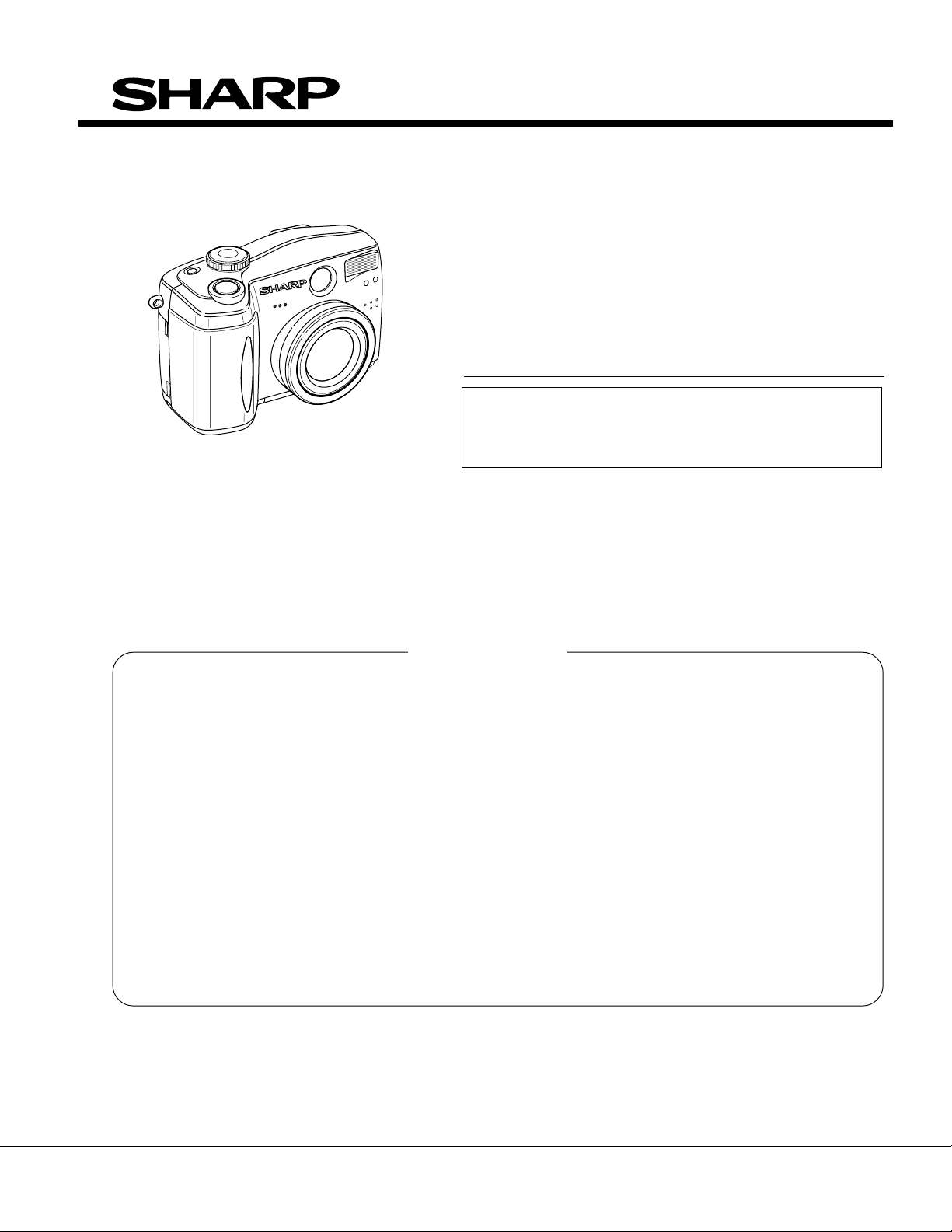
DIGITAL STILL CAMERA
VE-CG30U
VE-CG30U
VE-CG40U
MODELS
In the interests of user-safety (Required by safety regulations in some countries) the set should be resrored to its
original condition and only parts identical to those specified
be used.
VE-CG40U
CONTENTS
Page
1. IMPORTANT SERVICE NOTES ........................................................................................................ 2
2. SPECIFICATIONS .............................................................................................................................. 4
3. PART NAMES .................................................................................................................................... 5
4. DISASSEMBLY OF THE SET ............................................................................................................ 6
5. TEST MODE FUNCTION ................................................................................................................... 9
6. TROUBLESHOOTING...................................................................................................................... 19
7. BLOCK DIAGRAMS ......................................................................................................................... 24
8. SCHEMATIC DIAGRAMS ................................................................................................................ 30
9. SEMICONDUCTOR LEAD IDENTIFICATION ................................................................................. 64
10.PRINTED WIRING BOARD ASSEMBLIES ...................................................................................... 66
11.REPLACEMENT PARTS LIST / EXPLODED VIEWS...................................................................... 72
12.PACKING OF THE SET ................................................................................................................... 82
SHARP CORPORATION
This document has been published to be used for after
sales service only.
The contents are subject to change wthout notice.
1
Page 2
VE-CG30U
VE-CG40U
BEFORE RETURNING THE VIDEO CAMERA
RECORDER
Before returning the video camera recorder to the user,
perform the following safety checks.
1. Inspect all lead dress to make certain that leads are
2. Inspect all protective devices such as non-metallic
3. To be sure that no shock hazard exists, check for
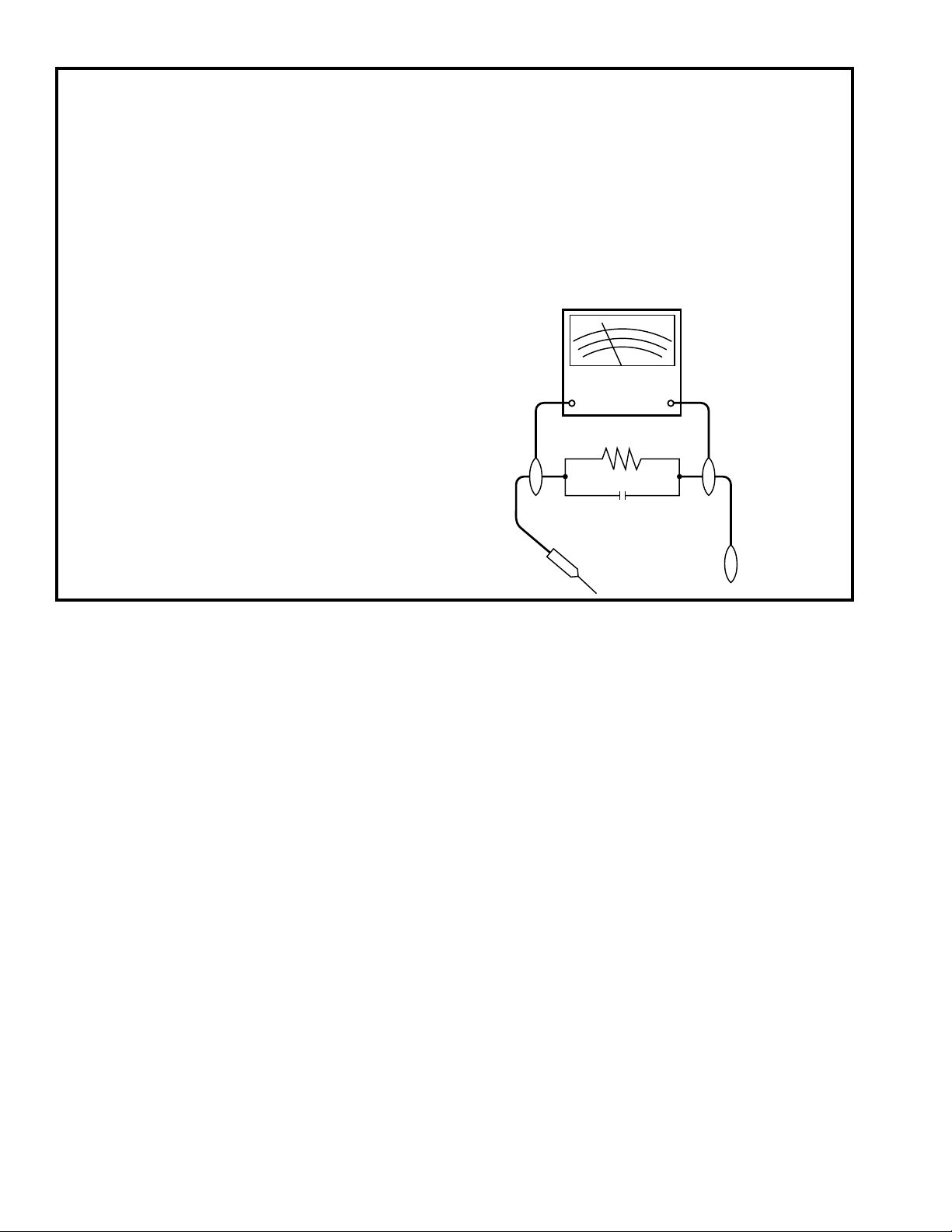
· Plug the AC line cord directly into a 120 volt AC outlet
· Using two clip leads, connect a l.5k ohm, 10 watt resistor
· Use a VTVM or VOM with 1000 ohm per volt, or higher
· Move the resistor connection to all exposed metal
1. IMPORTANT SERVICE NOTES
not pinched or that hardware is not lodged between
the chassis and other metal parts in the video camera
recorder.
control knobs, insulating materials, cabinet backs,
adjustment and compartment covers or shields, isolation resistor/capacitor networks, mechanical insulators etc.
leakage current in the following manner.
(Do not use an isolation transformer for this test).
paralleled by a 0.15µF capacitor in series with all
exposed metal cabinet parts and a known ground,
such as a water pipe or conduit.
sensitivity or measure the AC voltage drop across the
resistor (See Diagram).
parts having a return path to the chassis (antenna
connections, metal cabinet, screw heads, knobs and
control shafts, etc.) and measure the AC voltage drop
across the resistor. Reverse the AC plug (a non
polarized adaptor plug must be used but only for the
purpose of completing these checks) on the set and
repeat the AC voltage measurements for each exposed metallic part. Any reading of 0.45V rms (this
corresponds to 0.3mA rms AC.) or more is excessive
and indicates a potential shock hazard which must be
corrected before returning the video camera recorder
to the user.
VTVM
AC SCALE
1.5k ohms
10W
0.15 µF
TEST PROBE
TO EXPOSED
METAL PARTS
CONNECT TO
KNOWN EARTH
GROUND
2
Page 3
■ PRECAUTIONS FOR USING LEAD-FREE SOLDER
1) Employing lead-free solder
"Main PWB", "Camera head PWB", "Audio I/O PWB", "Card PWB", "Inverter PWB", "Operation PWB", "DC Jack
PWB", "CCD PWB" of this model employs lead-free solder. The LF symbol indicates lead-free solder, and is attached
on the PWBs and service manuals. The alphabetical character following LF shows the type of lead-free solder.
Example:
Indicates lead-free solder of tin, silver and copper
2) Using lead-free solder
When fixing the PWB soldered with the lead-free solder, apply lead-free wire solder. Repairing with conventional
lead wire solder may cause damage or accident due to cracks.
As the melting point of lead-free solder (Sn-Ag-Cu) is higher than the lead wire solder by 40°C, we recommend you
to use a dedicated soldering bit. If you are not familiar with how to obtain lead-free solder or soldering bit, contact
our service station or service ranch in your area.
VE-CG30U
VE-CG40U
3) Soldering
As the melting point of lead-free solder (Sn-Ag-Cu) is 220°C which is higher than the conventional lead solder by
40°C, and as it has poor solderability, you may be apt to keep the soldering bit in contact with the PWB for extended
period of time. However, since the land may be peeled off or the maximum heat-resistance temperature of parts may
be exceeded, remove the bit from the PWB as soon as you confirm the steady soldering condition.
Lead-free solder contains more tin, and the end of the soldering bit may be easily corroded. Make sure to turn on
and off the power of the bit as required.
If a different type of solder stays on the tip of the soldering bit, it is alloyed with lead-free solder. Clean the bit after
every use of it.
When the tip of the soldering bit is blackened during use, file it with steel wool or fine sandpaper.
Lead-free wire solder for servicing
Part No. ★ Description Price Code
ZHNDAi123250E J φ0.3mm 250g(1roll) BL
ZHNDAi126500E J φ0.6mm 500g(1roll) BK
ZHNDAi12801KE J φ1.0mm 1kg(1roll) BM
3
Page 4

VE-CG30U
VE-CG40U
2. SPECIFICATIONS
Digital still camera
Image Capturing Device 1/1.8" CCD image sensor (effective pixels: 4.04 megapixels(CG40U)
Color Temperature Compensation Auto white balance with daylight, fluorescent or tungsten
Sound Recording Format WAV (monaural) (CG40U ONLY)
Dimensions(W x H x D) 4.5" x 2.9" x 2.4" (113.5 x 74.5 x 60 mm)
Operating Temperature 32°F to 104°F (0°C to +40°C)
AC adapter
3.2megapixels(CG30U))
Lens F2.0-F2.5 f=7-21mm (35mm film equivalent: 33-99mm)
Power zoom 1-3x in optical range, 3-9x in digital range
LCD monitor 1.5" CGSilicon, 134,000pixels
Power Source AA size alkaline batteries
Ni-MH rechageble batteries
DC 6.0V with AC adapter
Power Consumption 3.2W (CG40U), 2.9W (CG30U)
Recording Format JPEG for still images
Motion JPEG for motion images (CG40U ONLY)
Recording Medium SD Memory Card
Weight 0.64lbs (290 g)(CG40U)(without batteries, card, wrist strap, and lens cap)
0.63lbs (285 g)(CG30U)(without batteries, card, wrist strap, and lens cap)
Storage Temperature -4°F to 140°F (-20°C to +60°C)
Operating Humidity 30% to 80%
Power Requirement AC 100-120V, 50/60Hz
DC Output 6V
Operating Temperature 32°F to 104°F (0°C to +40°C)
Dimetions (W x H x D) 2.0" x 1.1" x 2.6" (50.0 x 27.0 x 65.5 mm)
Weight 0.24 lbs (108g)
Specifications are sbject to change without notice.
SERVICE INFOMATION (FOR THE U.S.)
For the location of the nearest Sharp Authorized Service Center, or to obtain product literature, accessories,
supplies or customer assistance, please call 1-800-BE SHARP (1-800-237-4277) or visit SHARP's website
(http://www.sharpusa.com).
4
Page 5
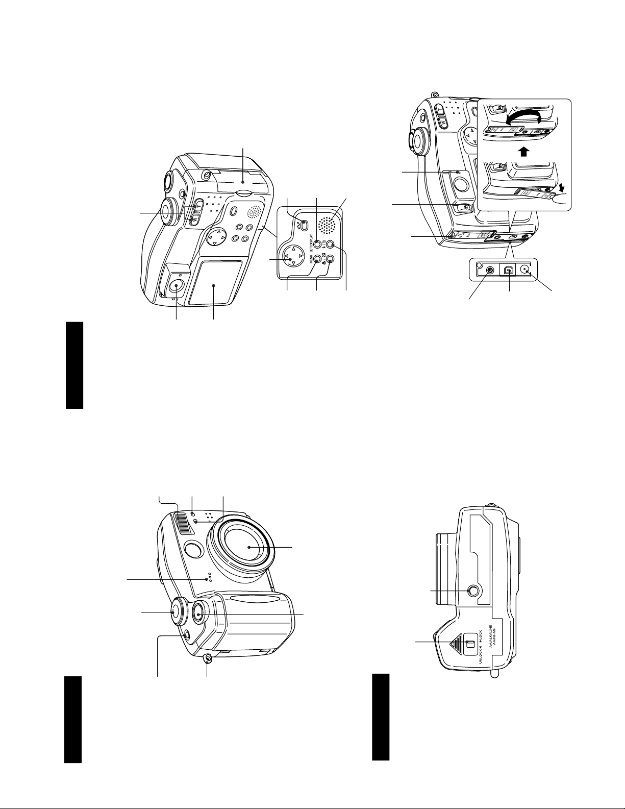
3. PART NAMES
Zoom lens
Microphone (CG40 ONLY)
Self timer indicator
Shutter button
Flash sensor
Flash
Wrist strap loop
Power button
Mode Dial
Battery compartment door release
Tripod socket
Front view
Bottom view
Rear view
SET/DISPLAY button
MENU button
Viewfinder
Power Zoom buttons (W: wide
angle,T: telephoto)
Speaker
Card slot cover
Macro /
Thumbnail
button
button
LCD screen
Flash /
Delete
Operation button
Data transfer button
A/V OUT jack (CG40U)
VIDEO OUT jack (CG30U)
USB terminal
DC IN jack
Jack cover
Diopter control
Status indicator
(CG40 ONLY)
For details on the use of each control.
VE-CG30U
VE-CG40U
5
Page 6
VE-CG30U
VE-CG40U
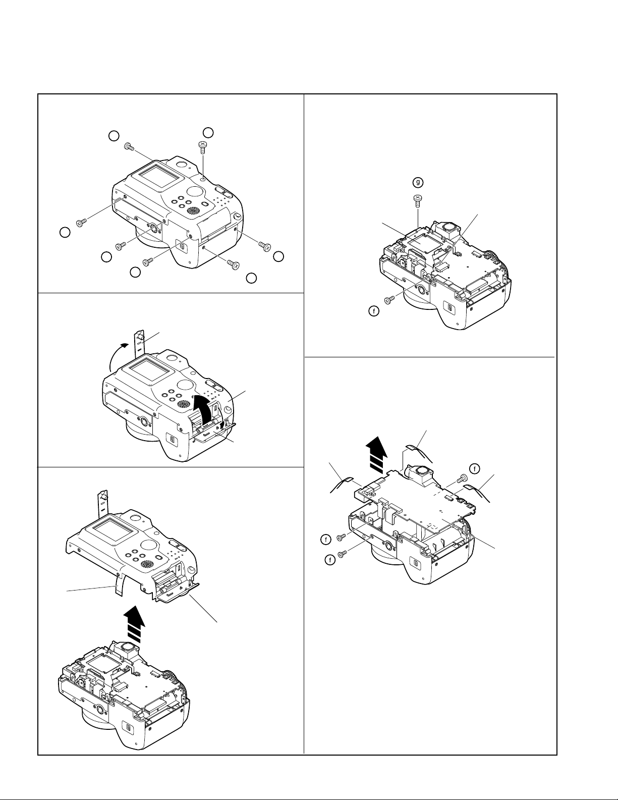
4. DISASSEMBLY OF THE SET
4-1. DISASSEMBLY OF THE SET
Note:
Before removing the cabinet, turn off the power supply, and ascertain that the battery have been removed.
Remove the five screws ((a)LX-HZ0063TAFF) and
1.
two screws ((h)XiPSF17P04000).
h
h
a
4.
After removing the one screw ((f)XiPSF17P03000)
and one screw ((g)XiPSN17P02000), disconnect
the connector and pull out the FFC to take out the
LCD unit.
LCD unit
FFC
a
a
2.
Open the media lid and jack cover, and then open the
a
back cabinet turning it.
Jack cover
Back cabinet
Media lid
3.
Disconnect the connector and pull out the FFC.
a
5.
After removing the three screws ((f)XiPSF17P03000),
disconnect the connector and pull out the three
FFCs.
Pull out the CCD PWB slightly.
FFC
FFC
FFC
FFC
CCD PWB
Be sure to keep the media
lid open when attaching
the back cabinet ass'y.
6
Page 7
VE-CG30U
VE-CG40U
6.
Disconnect the two connectors to take out the CCD
PWB.
Each connector has four wires.
(For 40U, disconnect the three connectors.)
Connector(CG40U only)
Connector
Connector
CCD PWB
8. Remove the four screws ((f)XiPSF17P03000)
to take out the AV jack PWB and strobe unit.
Caution:
Hold the transformer to remove the strobe unit.
AV jack PWB
Transformer
Strobe unit
7.
Remove the one screw ((b)LX-HZ0050TAFF) and
disconnect the connector to take out the top cabinet.
Connector
b
Caution: Electric shock
When disassembling or repairing the set, do not touch the high voltage section of the main capacitor
since it contains high voltage. Be especially careful when removing and mounting the screws of the jack
unit (DUNTKB359PM) and strobe unit as well as when replacing the wires (QCNW-A562/564/565WJ).
After removing the strobe unit, prepare the following discharging jig (1) and connect it to the (2) position
as shown in the figure. Discharge main capacitor by leaving discharge jig attached for 60 seconds.
Clip
High voltage section
Prepare approx. 5kΩ/5W.
Figure 1
+
-
Clip connection
7
Page 8
VE-CG30U
VE-CG40U
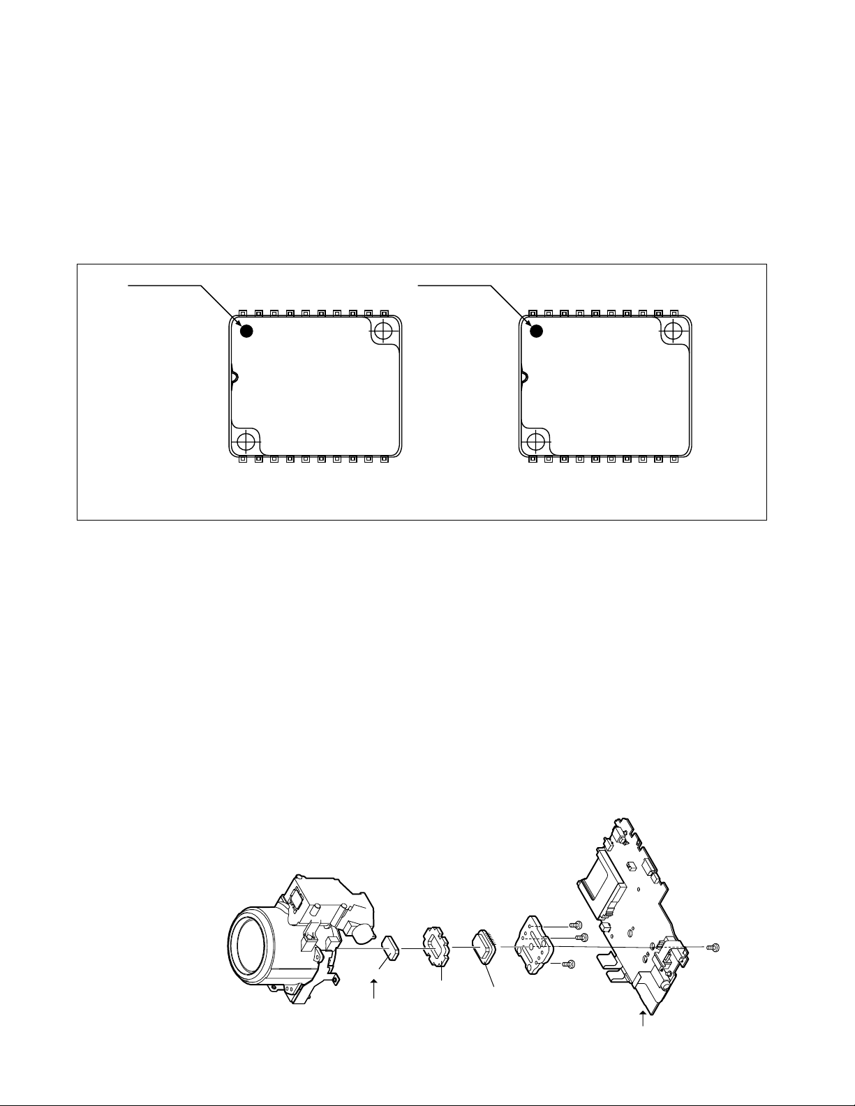
4-2. REPLACEMENT OF CCD SENSOR
4-2-1. BEFORE REPLACEMENT
1) The CCD image sensor is more sensitive to electrostatic breakage than C-MOS LSI.Therefore sufficient means
to prevent electrostatic damage must be taken when it is replaced.
• Ground the soldering iron.
• Ground also the human body, using the wrist strap(through an 1 M ohm resistor).
• Until the CCD sensor is mounted on the PWB, fit it to the conductive sponge, and short-circuit the foot lead.
2) Take utmost care so that the surface glass of CCD sensor and optical filter are not contaminated and damaged.
If any contamination is found, for example fingerprint, wipe it off with silicon paper or clean chamois skin.
3) When replacing the CCD sensor, use the static electricity prevention grounded soldering-iron, and perform
quickly soldering.
Index Mark
110
JAPAN
SHARP
RJ21P3
BA0PT
YYWWXX
20 11
Index Mark
110
JAPAN
SHARP
RJ21R3
BA0PT
YYWWXX
20 11
CG30 CG40
4-2-2. REMOVAL OF CCD
1) Unsolder the CCD sensor leads from the MAIN PWB.
2) Take out the MAIN PWB.
3) Remove the three screws (LX-HZ0013TAFF), and remove the sensor holder and CCD sensor.
4-2-3. MOUNTING OF CCD
1) Place the lens unit upright (since the CCD sensor mount ID faces upward, care must be taken so as not to
damage the front lens of unit), put the crystal filter first and then the dust protection rubber into the CCD holder
of lens unit.
Set the crystal unit with its thin side toward the lens unit.
2) Place the CCD sensor so that the its No. 1 pin is at the right lower (Positioning hole to be at right), and put the
CCD sensor into the CCD holder. For smooth and tight fitting, press the right lower part of back of CCD sensor,
and then press the left upper part.
Note: Pay attention to the direction of CCD sensor.
3) Place the sensor holder so that its two round markings be visible, and fix the sensor holder with the theree screws
(LX-HZ0013TAFF).
4) Mount the MAIN PWB so that the CCD sensor leads go thorough the PWB holes.
5) Solder the CCD sensor lead to the sensor PWB.
Note: Take care not to apply excessive heat.
*Refer to P.80
Crystal
PFiLWA025WJZZ (CG40U)
PFiLWA026WJZZ (CG30U)
8
Rubber
CCD
DUNTKB356QA00 (CG40U)
DUNTKB357QA00 (CG30U)
Page 9
VE-CG30U
VE-CG40U
5.TEST MODE FUNCTION
[Note]: The meaning of TEST MODE FUNCTION Under this test mode, following things can be done.
1; Check and change EEPROM values, if required. 2; Apply several tests and adjustments.
3; Check the version # of firmware.
How to enter the test mode (TEST MODE initial screen)
Reset the user mode settings first. Download the user mode settings reset program to the SD card to create a test mode
setting card. Regarding Test Mode Setting Program("Shce0009.dat" & "Shcu0009.dat"), please refer to Service
Information. Insert this SD card for resetting the user mode settings in the camera and turn on the power while pressing
shutter. Then, "do you vertion up?; Do: Push Shutter, No: Do Not" appears on the CGS display. Next press shutter to
set the factory mode setting. (If it is not mecessary to reset the user mode setting, turn off the power and remove the
SD card.) The message changes to "vertion up start", and "version up complete" appears soon. After checking that
the power has turned on, turn it off and remove the SD card. Now restting the default settings is finished.
Shutter
Do You VersionUp?
3X
OPTICAL ZOOM
DIGITAL STILL
Do : Push Shutter
No : Do Not
Power Key
Set the camera to the factory mode in the following procedure.
1) Turn on the power by pressing the power key with the MENU key pressed down.
2) When entering the test mode, the screen on the right(TEST MODE initial screen)
or key
Version Up Complete
TEST MODE initial screen
SET key
TEST MODE
BOOT VER xxxxx
IPL VER xxxxx
MAIN VER xxxxx
MENU Key
MENU Key
How to enter each test mode
1) Press the or key to select the desired test mode.
Each time you press the or key, each test item is displayed.
Test Nos. and the corresponding test items are as follows.
TEST NOS. Test item Display
TEST 0 EEPROM address change 0 CANGE E2PROM
TEST 1 LCD test pattern display 1 TEST PATERN
TEST 2 Default settings 2 SET SHIPPING
TEST 3 White balance low color temp. adjustment 3 WB LOW TEMP
TEST 4 White balance high color temp. adjustment 4 WB HIGH TEMP
TEST 5 CCD pixel defect correction 5 DEFECT WHT BLK
TEST 6 Not use in service 6 DEFECT WHT BLK
TEST 7 AF adjustment 7 FOCUS
TEST 8 Not use in service 8 CCD SENSITIVITY
TEST 9 Shutter timing adjustment (open side) 9 SHUTTER OPEN
TEST A Shutter timing adjustment (close side) A SHUTTER CLOSE
TEST B Not use in service B WB HIGH CALIB
TEST C Not use in service C LCD POSITION
TEST D Battery adjustment D BATTERY VOLTAGE
TEST E Not use in service E WB LOW CALIB
TEST F Not use in service F TEST F
2) If the desired test item is found, press the SET key to select it.
[Note]: When finishing the service works, the camera must be set USER MODE again. In order to set the camera back
to USER MODE, execute TEST 2 written as "User mode settings" on page 11.
SUB VER xxxxx
USB SNUM xxxxxxxx
0 CHANGE E2PROM
9
Page 10

VE-CG30U
VE-CG40U
5-1. Test mode specifications
5-1-1. TEST 0: EEPROM address change
[Note]: If address is selected and the data is changed during adjustment, the data of EEPROM is rewritten,
so take sufficient care for operation and never fail to take a memo of the address and the data before changing
the data.
When entering the test mode 0, the screen on the right appears.
[Operation]
1. Move the triangle mark ( ) to the digit to be changed using the or button.
Then change the address value with the or button as desired.
ADDRESS
0000
VALUE
ADDRESS
0100
VALUE
2. The value in the flash memory for the set address (upper line) and the initial
value (lower line) - if it has been set - are displayed under VALUE.
Example: With the initial value 0, the upper line shows FF and the lower
shows 01 at default.
3. When the address value is set, press the SET key to validate it.
( ) shifts to the value change mode.
4. As with the address value setting, change the value using the or and
or buttons.
5. When the value is set, press the SET key to validate it. ( ) shifts to the
address change mode.
6. When changing other address values, repeat from step 1.
<<When displaying the battery adjustment value>>
The battery adjustment correction value may be displayed in negative. If so, “-” is displayed in front of the value
(0000).
ADDRESS
0000
VALUE
ADDRESS
0010
VALUE
ADDRESS
0000
VALUE
ADDRESS
0001
VALUE
Set the address and press
the SET key.
( ) shifts to the value
change mode.
[Exit]
When setting is complete, perform either operation below.
• To select another test mode: Press the DELETE key to return to the TEST MODE initial screen.
• To end the test mode: Press the power key to turn off the camera.
ADDRESS
0000
VALUE
FF
01
0 CHANGE E2PROM
ADDRESS
0000
VALUE
FF
01
0 CHANGE E2PROM
5-1-2. TEST 1: LCD test pattern display
When entering the test mode 1, the screen below appears.
Test pattern
Magenta
Blue
Red Yellow
Green Gray
White
Cyan
1: Color bar
2: BLACK
3: BLUE 10%
4: GREEN 50%
5: RED 30%
6: 50% WHITE
7: 30% WHITE
8: CROSS HATCH
9: 14 Steps Gray Scale
10
[Operation]
• Press the or button to switch the test
pattern. See above for available test
patterns.
• Press the DELETE key to return to the
TEST MODE initial screen.
Page 11

5-1-3. TEST 2: User mode settings
When finishing the service works, the camera must be set USER MODE again.
In order to set the camera back to USER MODE, execute TEST 2 as below.
VE-CG30U
VE-CG40U
Select the TEST 2 and press the SET key.
TEST MODE
BOOT VER xxxxx
IPL VER xxxxx
MAIN VER xxxxx
SUB VER xxxxx
USB SNUM xxxxxxxx
2 SET SHIPPING
ENTER : START
DEL : RETURN
2 SET SHIPPING
TEST MODE 2 screen After settng
[Operation]
· Press the SET key start to [User Mode settings].
· When completed, the screen below appears.
COMPLETE
DEL RETURN
2 SET SHIPPING
00XX
00XX
0000
0000
0000
· Press the power key to end the test mode.
TEST 3,4,5,7,9,A and D are test modes for camera adjustment. See "5-2 Adjustment method" for detailed test
environment.
5-1-4. TEST 3: White balance low color temp.
adjustment
Select the TEST 3 and press the SET key.
TEST MODE
BOOT VER xxxxx
IPL VER xxxxx
MAIN VER xxxxx
SUB VER xxxxx
USB SNUM xxxxxxxx
3 WB LOW TEMP
ENTER : START
DEL : RETURN
3 WB LOW TEMP
TEST MODE 3 screen After settng
[Operation]
· Press the SET key to start adjustment.
· When completed, the screen below appears.
COMPLETE
DEL RETURN
3 WB LOW TEMP
· To select another test mode:
Press the DELETE key to return to the TEST MODE
initial screen.
· To end the test mode:
Press the POWER key to turn off the camera.
00XX
00XX
0000
0000
0000
[Operation]
· Press the SET key to start adjustment.
· When completed, the screen below appears.
COMPLETE
DEL RETURN
4 WB HIGH TEMP
00XX
00XX
0000
0000
0000
· To select another test mode:
Press the DELETE key to return to the TEST MODE
initial screen.
· To end the test mode:
Press the POWER key to turn off the camera.
5-1-6. TEST 5: CCD pixel defect correction.
adjustment
Select the TEST 5 and press the SET key.
TEST MODE
BOOT VER xxxxx
IPL VER xxxxx
MAIN VER xxxxx
SUB VER xxxxx
USB SNUM xxxxxxxx
5 DEFECT WHT BLK
ENTER : START
DEL : RETURN
5 DEFECT WHT BLK
TEST MODE 5 screen After settng
5-1-5. TEST 4: White balance high color temp.
adjustment
Select the TEST 4 and press the SET key.
TEST MODE
BOOT VER xxxxx
IPL VER xxxxx
MAIN VER xxxxx
SUB VER xxxxx
USB SNUM xxxxxxxx
4 WB HIGH TEMP
TEST MODE 4 screen After settng
ENTER : START
DEL : RETURN
4 WB HIGH TEMP
[Operation]
· Press the SET key to start adjustment.
· When completed, the screen below appears.
COMPLETE
DEL RETURN
5 DEFECT WHT BLK
· To select another test mode:
Press the DELETE key to return to the TEST MODE
initial screen.
· To end the test mode:
Press the POWER key to turn off the camera.
11
0XXX
0XXX
0XXX
0XXX
0XXX
Page 12

VE-CG30U
ENTER : START
DEL : RETURN
A SHUTTER OPEN
ENTER : START
DEL : RETURN
D BATTERY VOLTAGE
VE-CG40U
5-1-7. TEST 7: AF adjustment
Select the TEST 7 and press the SET key.
TEST MODE
BOOT VER xxxxx
IPL VER xxxxx
MAIN VER xxxxx
SUB VER xxxxx
USB SNUM xxxxxxxx
7 FOCUS
ENTER : START
DEL : RETURN
7 FOCUS
TEST MODE 7 screen After settng
[Operation]
· Press the SET key to start adjustment.
· When completed, the screen below appears.
COMPLETE
DEL RETURN
7 FOCUS
· To select another test mode:
Press the DELETE key to return to the TEST MODE
initial screen.
· To end the test mode:
Press the POWER key to turn off the camera.
0XXX
0XXX
0XXX
0XXX
0XXX
5-1-9. TEST A: Shutter timing adjustment (open
side)
Select the TEST A and press the SET key.
TEST MODE
BOOT VER xxxxx
IPL VER xxxxx
MAIN VER xxxxx
SUB VER xxxxx
USB SNUM xxxxxxxx
A SHUTTER OPEN
TEST MODE A screen After settng
[Operation]
· Press the SET key to start adjustment.
· When completed, the screen below appears.
COMPLETE
DEL RETURN
A SHUTTER OPEN
· To select another test mode:
Press the DELETE key to return to the TEST MODE
initial screen.
· To end the test mode:
Press the POWER key to turn off the camera.
0XXX
0XXX
0XXX
0XXX
0XXX
5-1-8. TEST 9: Shutter timing adjustment (close
side)
Select the TEST 9 and press the SET key.
TEST MODE
BOOT VER xxxxx
IPL VER xxxxx
MAIN VER xxxxx
SUB VER xxxxx
USB SNUM xxxxxxxx
9 SHUTTER CLOSE
ENTER : START
DEL : RETURN
9 SHUTTER CLOSE
TEST MODE 9 screen After settng
[Operation]
· Press the SET key to start adjustment.
· When completed, the screen below appears.
COMPLETE
DEL RETURN
9 SHUTTER CLOSE
· To select another test mode:
Press the DELETE key to return to the TEST MODE
initial screen.
· To end the test mode:
Press the POWER key to turn off the camera.
0XXX
0XXX
0XXX
0XXX
0XXX
5-1-10. TEST D: Battery adjustment (open side)
Select the TEST D and press the SET key.
TEST MODE
BOOT VER xxxxx
IPL VER xxxxx
MAIN VER xxxxx
SUB VER xxxxx
USB SNUM xxxxxxxx
D BATTERY VOLTAGE
TEST MODE D screen After settng
[Operation]
· Press the SET key to start adjustment.
· When completed, the screen below appears.
COMPLETE
DEL RETURN
D BATTRY VALTAGE
· To select another test mode:
Press the DELETE key to return to the TEST MODE
initial screen.
· To end the test mode:
Press the POWER key to turn off the camera.
00XX
00XX
0000
0000
0000
12
Page 13
5-2. Adjustment method
<Neccesary object of shooting, measuring instrument and jigs>
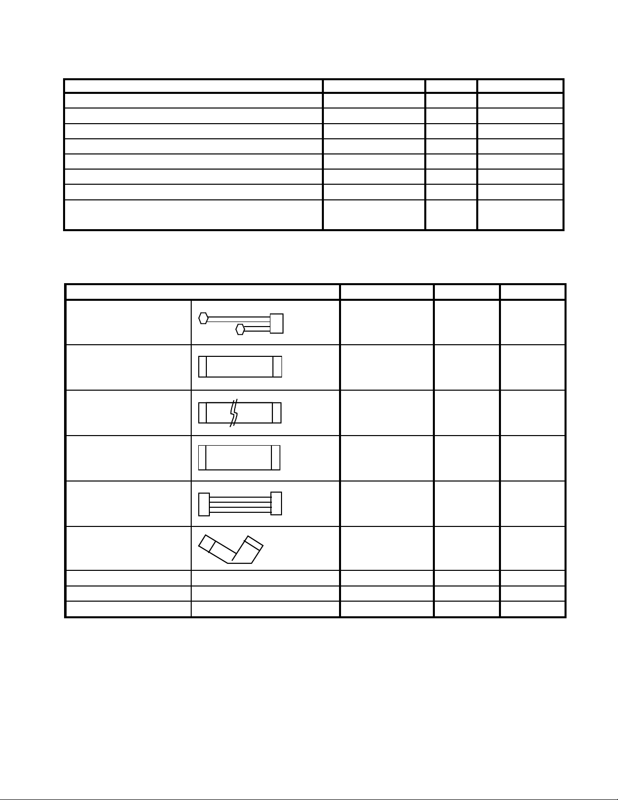
Jig name Part code
AC adapter UADP-A013WJZZ AY
2 halogen lamps Commerical item –
Gray scale chart JiGCHART-1 CP
Color Bar Chart JiGCHART-4 DA
Siemens star chart JiGCHART-11 CE
Illuminometer (0-3000 lux) JiGMETER-1 CT
Color temperature meter (1600 - 400000K) JiGMETER-3 FF
Color temperatute conversion filter (3200 - 6800K) JiGHOYA-LB165 BN
HOYA "LB-165"
<Extention Cable etc.>
Jig name Part code
Price code
Price code
VE-CG30U
VE-CG40U
Remarks
Remarks
BATT.IN CHECK
Shutter PWB - Main PWB
Jack PWB - Main PWB *
&
Operation PWB - Main PWB
Strobe Unit - Main PWB
Jack PWB Main PWB
LCD I/F PWB Main PWB
ø3.5 A/V Cable
ø3.5 Video Cable
USB Cable
P=0.5mm
FFC
8 pin
P=0.5mm
FFC
10 pin
P=0.5mm
FFC
15 pin
4 pin
Wire A'ssy
P=0.5mm
FFC
18 pin
QTANZA006WJZZ AG
QCNW-A561WJZZ AB
QCNW-A563WJZZ AC
QCNW-A564WJZZ AC
QCNW-A565WJZZ AD
QCNW-A566WJZZ AC
QCNWGA016WJZZ AH
QCNWGA017WJZZ AH
QCNWGA018WJPZ AL
* QCNW-A562WJZZ (P=0,5mm, FFC, 10 pin) is used for "Jack PWB - Main PWB" in production.
13
Page 14
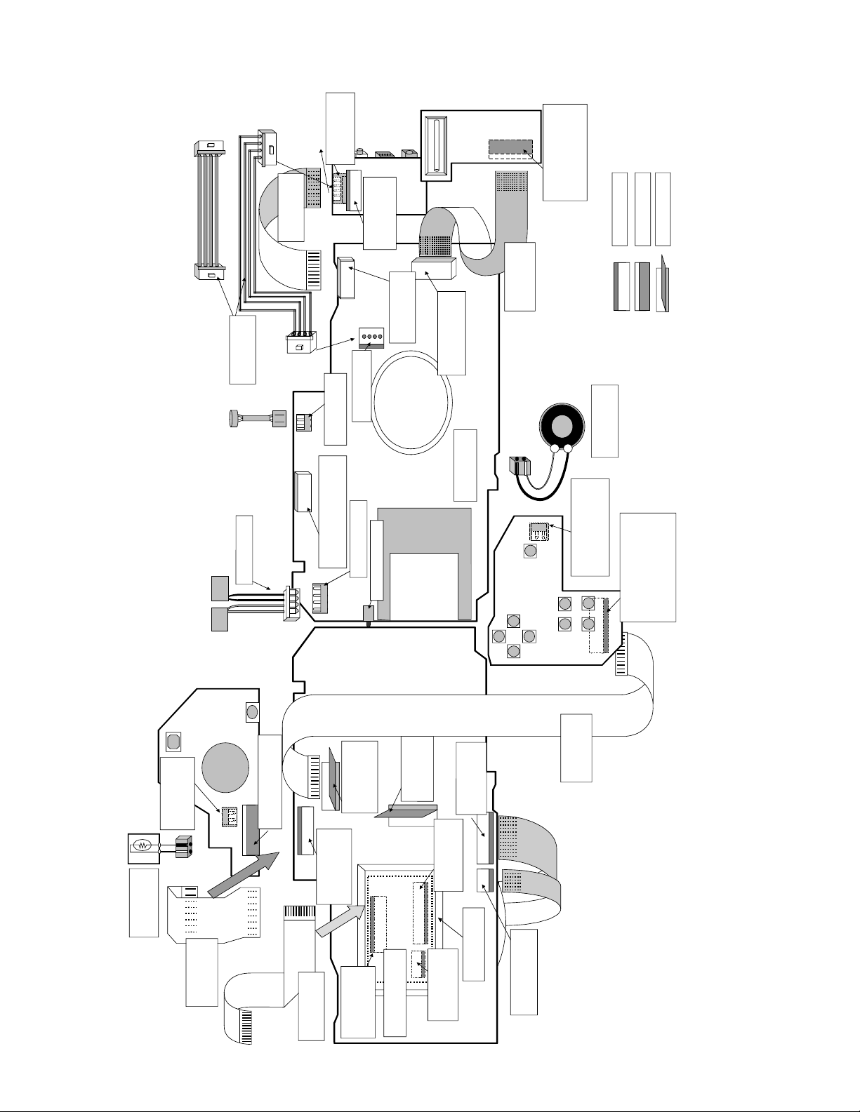
VE-CG30U
12
Mic.
14
2
1
reverse contact
normal contact
normal contact
1
2
2 1
—
+
1: GND
2: GND
3: VCC
4: VCC
SC7201 TO:MAIN
QSOCN0871TAZZ
(normal contact)
SC702
QSOCN1098TAZZY
(normal contact)
To: Operation
SC202
QSOCN0825TAN1Y
(reverse contact)
To:TOP(Shutter)
SC702
QSOCN1898TAZZY
(normal contact)
SC1002
QSOCN0672TAZZY
(reverse contact)
CGS IF PWB
Parts are monted on the back.
SC1802
QSOCN1872TAZZY
(reverse contact)
To: MAIN
18 pin FFC
QCNW-A566WJZZ
CGS IF - MAIN
8 pin FFC
QCNW-A561WJZZ
TOP - MAIN
P7201
QPLGN0276TAZZY
1mm pitch
(mounted on the back)
SC1801
QSOCN2472TAZZY
(reverse contact)
RUNTKA028WJZZ
TEMP.DET.
SC1803
QSOCN0672TAZZY
(reverse contact)
SC1001
QSOCN1672TAZZY
(reverse contact)
SC7201
QSOCN1872TAZZ
P2902
QPLGN0463TAZZY
SC401 (JACK)
QSOCN1007REN1
NON-ZIF Type
QSW-MA001WJZZY
SC4401
QSOCN1072TAZZY
TO : MAIN
(reverse contact)
10 pin FFC
QCNW-A562WJZZ
Jack - MAIN
4 pin Wire
QCNW-A565WJZZ
Jack - MAIN
P4401
QPLGN0463TAZZY
(mounted on the back)
P1602 (MIC)
QPLGN0274TAZZY
QTANZA006WJZZ
SC701
Do not care (Factory use)
QSOCN1007REN1
NON-ZIF Type
P2901 (DC-IN)
QPLGN0458REZZY
SC1701
QSOCN1025TAN1Y
(reverse contact)
TO : MAIN
(mounted on the back)
QSOCN1571TAZZY
TO : MAIN
(normal contact)
(mounted on the back)
SC201 (SD Card)
QSOCZA035WJZZY
Speaker
VSPA016P-F18N
P1701
QPLGN0276TAZZY
1 mm pitch
(mounted on the back)
15 pin FFC
QCNW-A564WJZZ
STROBE - MAIN
SC3001 (STROBE)
QSOCN1507REN1Y
NON-ZIF Type
1: GND
2: GND
3: VCC
4: VCC
4: GND
3: GND
2: VCC
1: VCC
4: GND
3: GND
2: VCC
1: VCC
1: GND
2: GND
3: VCC
4: VCC
10 pin FFC
QCNW-A563WJZZ
OPE - MAIN
VE-CG40U
CONNECTOR LAYOUT DRAWING
VE-CG40U
14
Page 15
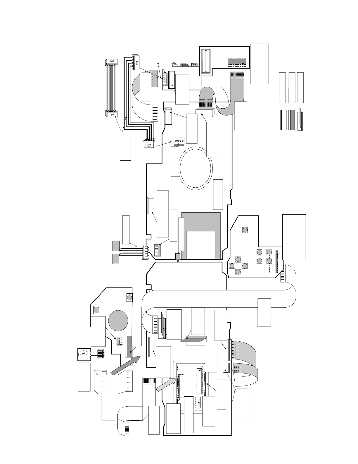
12
14
reverse contact
normal contact
normal contact
—
+
1: GND
2: GND
3: VCC
4: VCC
SC7201 TO:MAIN
QSOCN0871TAZZ
(normal contact)
SC702
QSOCN1098TAZZY
(normal contact)
To: Operation
SC202
QSOCN0825TAN1Y
(reverse contact)
To:TOP(Shutter)
SC702
QSOCN1898TAZZY
(normal contact)
SC1002
QSOCN0672TAZZY
(reverse contact)
CGS IF PWB
Parts are monted on the back.
SC1802
QSOCN1872TAZZY
(reverse contact)
To: MAIN
18 pin FFC
QCNW-A566WJZZ
CGS IF - MAIN
8 pin FFC
QCNW-A561WJZZ
TOP - MAIN
P7201
QPLGN0276TAZZY
1mm pitch
(mounted on the back)
SC1801
QSOCN2472TAZZY
(reverse contact)
RUNTKA028WJZZ
TEMP.DET.
SC1803
QSOCN0672TAZZY
(reverse contact)
SC1001
QSOCN1672TAZZY
(reverse contact)
SC7201
QSOCN1872TAZZ
P2902
QPLGN0463TAZZY
SC401 (JACK)
QSOCN1007REN1
NON-ZIF Type
QSW-MA001WJZZY
SC4401
QSOCN1072TAZZY
TO : MAIN
(reverse contact)
10 pin FFC
QCNW-A562WJZZ
Jack - MAIN
4 pin Wire
QCNW-A565WJZZ
Jack - MAIN
P4401
QPLGN0463TAZZY
(mounted on the back)
QTANZA006WJZZ
SC701
Do not care (Factory use)
QSOCN1007REN1
NON-ZIF Type
P2901 (DC-IN)
QPLGN0458REZZY
SC1701
QSOCN1025TAN1Y
(reverse contact)
TO : MAIN
(mounted on the back)
QSOCN1571TAZZY
TO : MAIN
(normal contact)
(mounted on the back)
SC201 (SD Card)
QSOCZA035WJZZY
15 pin FFC
QCNW-A564WJZZ
STROBE - MAIN
SC3001 (STROBE)
QSOCN1507REN1Y
NON-ZIF Type
1: GND
2: GND
3: VCC
4: VCC
4: GND
3: GND
2: VCC
1: VCC
4: GND
3: GND
2: VCC
1: VCC
1: GND
2: GND
3: VCC
4: VCC
10 pin FFC
QCNW-A563WJZZ
OPE - MAIN
CONNECTOR LAYOUT DRAWING
VE-CG30U
VE-CG30U
VE-CG40U
15
Page 16
VE-CG30U
B
VE-CG40U
5-2-1. Power circuit adjustment
Conditions
Mode dial setting: AUTO
Measuring instrument: Digital voltmeter
Adjustment jig: Dummy load is connected to
each TL.
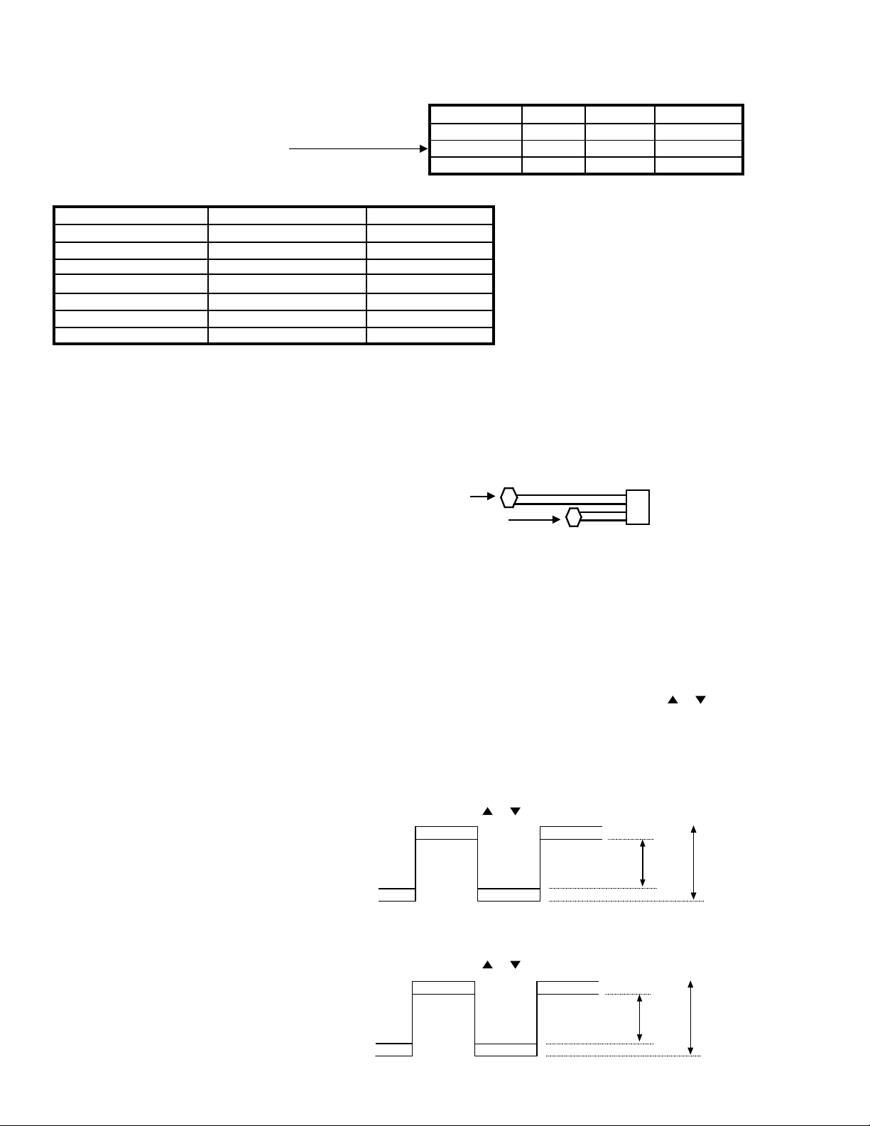
Line name TL Current Resistance
LCD 12.0V TL5904 8.6mA 1.4KΩ
CAM 15.0V TL1 10.0mA 1.4KΩ
CAM -7.0V TL3 8.0mA 0.8KΩ
5-2-1-1. Power line voltage check
Power line name Measuring point (TL) Measured value
1.APCON 5V TL3901 5.0±0.1V
2.APCON 3.3V TL4901 3.3±0.1V
3.DPCON 3.3V TL4902 3.3±0.1V
4.DPCON 1.8V TL6901 1.8±0.1V
5.LCD 12V TP5903 12.0±0.4V
6.CAM 15V TL5901 15.0±0.5V
7.CAM -7.0V TL5902 -7.0±0.35V
5-2-1-2. Temperature detection function check
Connect a resistor of 680Ω between TL770 and GND and check that the power is turned off.
5-2-1-3. Battery shutoff voltage adjustment
1) Connect the BTT.IN Check jig (QTANZA006WJZZ) to the main PWB P2902.
2) Apply 3.90±0.03V between the positive (+) and negative (-) electrodes of the BATT.IN Check jig (QTANZA006WJZZ).
3) According to the procedure of 5-1, set <TEST D> and press the SET key to adjust the voltage.
Long : (-)
Short : (+)
BATT.IN Check jig (QTANZA006WJZZ)
5-2-2. LCD circuit adjustment
Conditions
Mode: Set <TEST 0> according to the procedure of 5-1 and select the ADDRESS value which is specified in the
following adjustment items. Set E2PROM data to the value specified in the adjustment procedure. See 5-1-1.
Measuring instrument: Digital voltmeter, oscilloscope
5-2-2-1. VCO adjustment
Address: 0518 (1) Connect the digital voltmeter to TL1819.
Measuring point: TL1819 (2) Select the address 0518 and set the address. (No signal on the LCD Display)
TL1818 (GND) (3) Set the data of the DC voltage to a specified value using or key.
Adjustment specification: 1.66V±0.1V
5-2-2-2. R-W/B ADJ
Address: 0501 (1) Connect the oscilloscope to TL1837 (G-OUT)/TL1838 (R-OUT).
Measuring point: TL1837 (G-OUT) (2) Select the address 0501 and set the address. (No signal on LCD Display)
TL1838 (R-OUT) (3) Adjust the difference between peak-to-peak values of TL1837 (G-OUT)
TL1832 (GND) and TL1838 (R-OUT) using or key.
Adjustment specification: 0V±0.05V
GR
5-2-2-3. B-W/B ADJ
Address: 0502 (1) Connect the oscilloscope to TL1837 (G-OUT)/TL1836 (B-OUT).
Measuring point: TL1837 (G-OUT) (2) Select the address 0502 and set the address. (No signal on LCD Display)
TL1836 (B-OUT) (3) Adjust the difference between peak-to-peak values of TL1837 (G-OUT)
TL1832 (GND) and TL1838 (R-OUT) using or key.
Adjustment specification: 0V±0.05V
G
16
Page 17

VE-CG30U
VE-CG40U
5-2-2-4. Common bias DC voltage adjustment
Address: 0509 (1) Connect the digital voltmeter to TL1842.
Measuring point: TL1842 (2) Select the address 0509 and set the address.
TL1832 (GND) (Color Bar pattern appears onLCD Display)
(3) Set the data of the DC voltage to a specified value using or key.
Adjustment specification: 6.3V±0.1V
5-2-2-5. Video output level adjustment
Address: 0065 (1) Connect the oscilloscope to TL407.(Video out; 75Ω termination)
Measuring point: TL407 (2) Select the address 0065 and set the address. (No signal on LCD Display)
TL411 (GND) (3) Set the level of H-SYNC to the adjustment specified value using or key.
Adjustment specification: 0.28V±0.01Vp-p
5-2-3. Camera circuit adjustment
• Preparation before adjustment and check items
(1) Illuminate the entire pattern evenly with luminance of approx. 2000 lux(In the white chart) (2 or more light sources
are recommended). Set the color temperature to 3200K.
(2) Use a new test pattern with no soil or color degradation.
(3) If defects are found in the electric circuit, identify the defective part using the measuring instrument and repair/
replace it before adjustment.
5-2-3-1. Focus infinity adjustment
[Purpose]
Focus point in each zoom position of the lens is memorized to correct the focus tracking position when operating
the zoom lens.
[Object]
Siemens Star Chart via the collimator or an object with simple and distinct outline.
If you do not have a collimator, perform adjustment while shooting an object with distinct outline from a long
distance.
Since the lens is automatically moved from Wide to Tele during adjustment, do not put an object in front of the
camera (do not shoot an object with a distinct outline when the lens is located at Wide).
[Procedure]
• After making the settings above, set <TEST 7> according to the procedures of 5-1 and execute it.
• Auto adjustment is performed.
Each optical zoom position is set, and the focus infinity position at that time is stored in memory.
• During adjustment, <EXECUTING> and the object are displayed on the LCD monitor.
• Data is collected while changing the zoom from Wide to Tele. Do not place any obstacles in front of the camera
until the adjustment is completed.
• If <OK> appears on the LCD monitor, adjustment is completed.
5-2-3-2. Adjustment for CCD pixel defect detection
[Purpose]
To memorize and correct the CCD imager’s white balance defect in the dark and black balance defect in the
brightness.
[Object]
An evenly illuminated white object under the lighting described in “Preparation before adjustment and check
items” (a light box can be used).
[Procedure]
• After making the settings above, set <TEST 5> according to the procedures of 5-1 and execute it.
• Auto adjustment is executed.
The lens is automatically shielded from the light and white balance in the dark is corrected.
Next, the aperture of the lens is automatically opened and black balance in the brightness is corrected while
a white object is shot.
• During adjustment, <EXECUTING> and the object appear on the LCD monitor.
• If <OK> appears on the LCD monitor, adjustment is completed.
17
Page 18

VE-CG30U
VE-CG40U
5-2-3-3. Mechanical shutter open aperture adjustment/CCD sensitivity adjustment
[Purpose]
• Brightness of the optical system including the CCD imager is adjusted to obtain ISO100.
• Operation time in the open state of the mechanical shutter aperture is memorized and the variation of exposing time
is removed.
[Object]
• An evenly illuminated white object under the lighting described in “Preparation before adjustment and check
items”.
[Procedures]
• After making the settings above, set <TEST 9> according to the procedures of 5-1 and execute it.
• Auto adjustment is executed.
• During adjustment, <EXECUTING> and the object are displayed on the LCD monitor.
• If <OK> appears on the LCD monitor, adjustment is completed.
• With <TEST 9>, the mechanical shutter opening adjustment and the CCD sensitivity adjustment are executed.
5-2-3-4. Mechanical shutter closed aperture adjustment
[Purpose]
• Operation time in the closed state of the mechanical shutter aperture is memorized and the variation of
exposing time is removed.
[Object]
• An evenly illuminated white object under the lighting described in “Preparation before adjustment and check
items”.
[Procedures]
• After making the settings above, set <TEST A> according to the procedures of 5-1 and execute it.
• Auto adjustment is executed.
• During adjustment, <EXECUTING> and the object are displayed on the LCD monitor.
• If <OK> appears on the LCD monitor, adjustment is completed.
5-2-3-5. WB low color temperature adjustment
[Purpose]
• The variation of CCD spectral characteristic (R, G, B) at low color temperature (3200K) is removed.
[Object]
• An evenly illuminated white object under the lighting described in “Preparation before adjustment and check
items”.
[Procedure]
• After making the settings above, set <TEST 3> according to the procedures of 5-1 and execute it.
• Auto adjustment is executed.
• During adjustment, <EXECUTING> and the object appear on the LCD monitor.
• If <OK> appears on the LCD monitor, adjustment is completed.
5-2-3-6. WB high color temperature adjustment
[Purpose]
• The variation of CCD spectral characteristic (R, G, B) at high color temperature (outside light, etc.) is removed.
[Object]
• An evenly illuminated white object under the lighting described in “Preparation before adjustment and check
items”.
• Mount the color temperature conversion filter LB165 in front of the lens.
[Procedure]
• After making the settings above, set <TEST 4> according to the procedures of 5-1 and execute it.
• Auto adjustment is executed.
• During adjustment, <EXECUTING> and the object appear on the LCD monitor.
• If <OK> appears on the LCD monitor, adjustment is completed.
18
Page 19
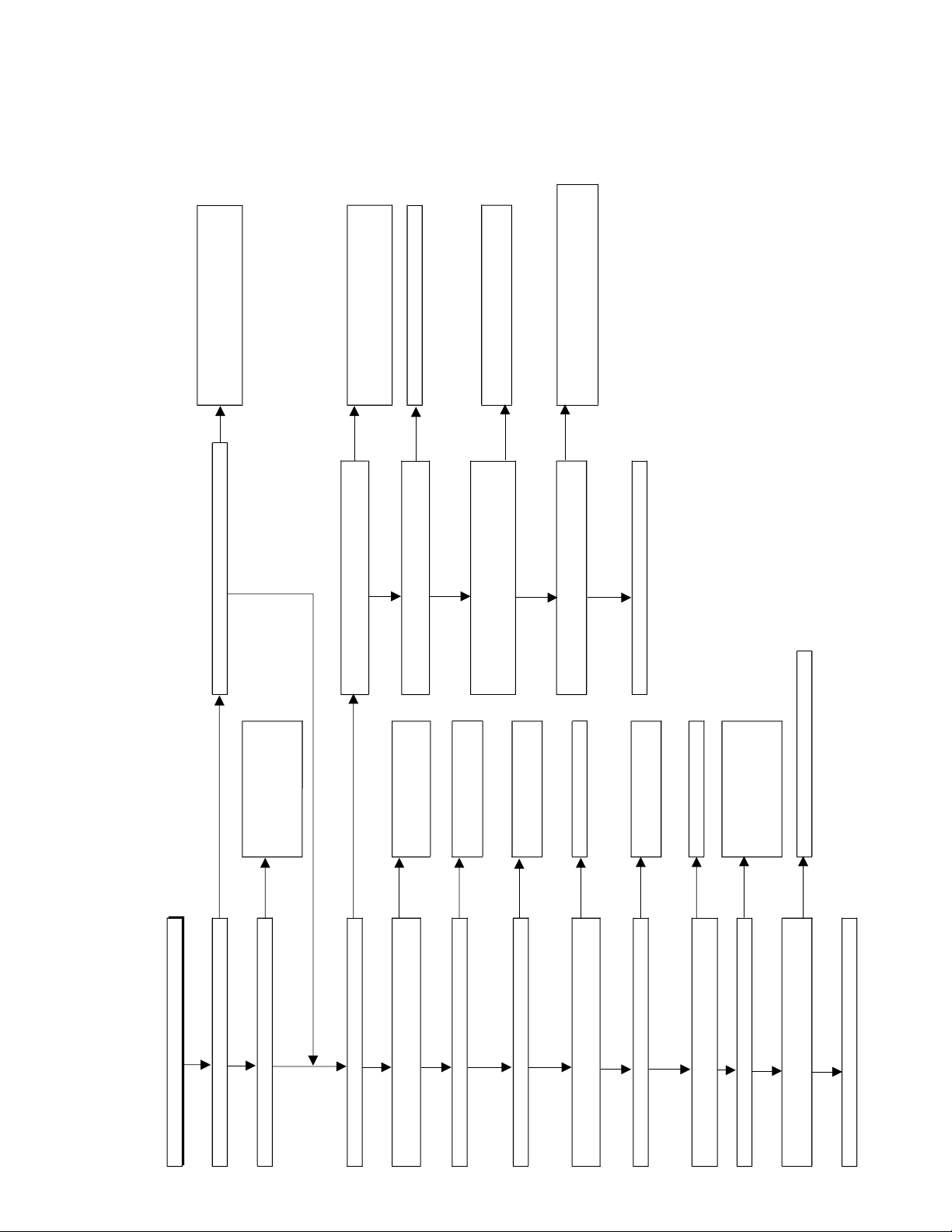
Power circuit troubleshooting
Power does not turn on.
Yes
Battery input
Check battery, battery terminals,
F2902, FB2901, FB2902, IC2901,
and R2901 - 2904.
Which is used, battery or DC input? When using DC input, does power turn on with battery?
DC input
Yes
Check AC adapter, DC jack,
FFC connection bet. JACK
PWB and MAIN (improper
insertion), F2901, and D2902.
When using battery, does power turn on with DC input?
No
No
Yes
Is P-CON-H sent to IC1901 6PIN?
Is 3.3V applied to TL7901?
Check soldering of IC702 33PIN and
IC1901 6PIN.
Check R1926.
Yes
Yes
No
Is triangular wave delivered to IC1901 7PIN even
for a moment?
Check IC1901 8PIN and
9PIN soldering, R1906, and
C1902.
No
Yes
Is pulse delivered to IC702 40PIN?
Check IC7901, C7901, and C7902.
No
Is voltage applied to D3901 cathode?
Check D3901, L3901, and
Q3901.
Yes
Yes
No
No
When Power SW is pressed, IC702 (43) pin falls
to "L".
Check IC702 40PIN and 41PIN, and
FL701.
Is 1.8V applied to TL6901 even for a moment?
Check Q6901, L6901, and
L6902.
Yes
No
No TOP PWB: Check power SW, connector and
harness.
MAIN: Check SC202 and R706.
Is 3.5V applied to both ends of C4902 even for a
moment?
Check Q4901 and L4901.
Yes
Yes
No
Check IC4902, R4904, and
and IC702 34PIN.
Is 3.3V applied to TL4902 even for a moment? Failure inside IC702.
Yes
No
Is voltage (NONREG) applied to T5901 3PIN and
4PIN?
Check Q5901 and R5901.
Yes
No
Check T5901, D5902, C5904,
D5901, C5903, L5901,
C5911, L5902, and C5907.
Is 15V applied to both ends of C5904?
Yes
Though voltage is applied to all power lines, power
does not turn on (LED and LCD are not lit).
No
Check power lines again.
Yes
FL201 or IC204(ASIC) failure.
Is voltage (3V) applied to IC702 33PIN(P-CON-H) ?
No
VE-CG30U
VE-CG40U
6.TROUBLESHOOTING
19
Page 20
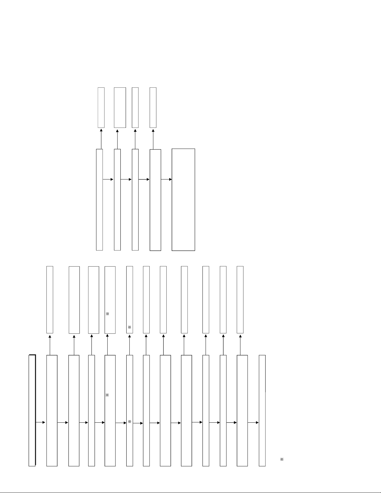
VE-CG30U
Camera troubleshooting
No
Yes
No
Check IC2 (in the checkable range since it is CSP).
Yes
No
No
Yes
Yes
No
No
Yes
Yes
No
No
Yes
Yes
No
No
Yes
Yes
No
Yes
No
Yes
No
Yes
No
Yes
No
Yes
Set mode SW to AUTO or MOV.
Is power voltage of CAM_5V, CAM_3.3V,
CAM_15V, and CAM_-7V normal?
Is LCD monitor normal?
Is OSD delivered?
Refer to LCD troubleshooting.
Refer to power troubleshooting.
Is pulse signal sent to TL4-TL13 of
IC1, 15V to TL1,
and -7V to TL3?
Check IC1 peripheral circuit
and IC2.
Is X1 oscillating?
Check IC4 and its peripheral
circuit.
Is signal delivered o
IC1 (20) pin (TL14)?
IC1 failure
Is signal sent to IC3 (30) pin?
Check Q2 and C26.
Is power [3.3V] of (13)(18)(24)(27)(33)(34)(40) of IC3
normal?
Check L4 and L5.
Is pulse signal sent to (16)(19)(20)(21)(22)(23) pins of
IC3?
Check IC2.
Is pulse signal sent to IC3 (46)(47)(48) pin?
Check IC204.
Check periphery of IC204.
Does IC204 operate normally?
Is video composite signal sent from (23) pin?
IC1 corresponds to the part 103 of the Camera Exploded View on page 82.
Are 10-bit signals (3) - (12) of IC3 sent?
IC3 failure
Check IC401 and its peripheral circuit.
L3 failure.
Is power supplied to L3[3.3V] ?
Is clock delivered from R15[CCDCLK]?
Check IC4 peripheral
circuit.
Is pulse delivered to R36[HD], R38[VD]?
Check IC204.
Is serial transfer pulse delivered to R33, R34, and
R35?
Check IC204.
Check whether pulse is delivered from each output
terminal of IC2. If there are terminals which do not
emit it, solder unwetting or IC failure.
VE-CG40U
20
Page 21
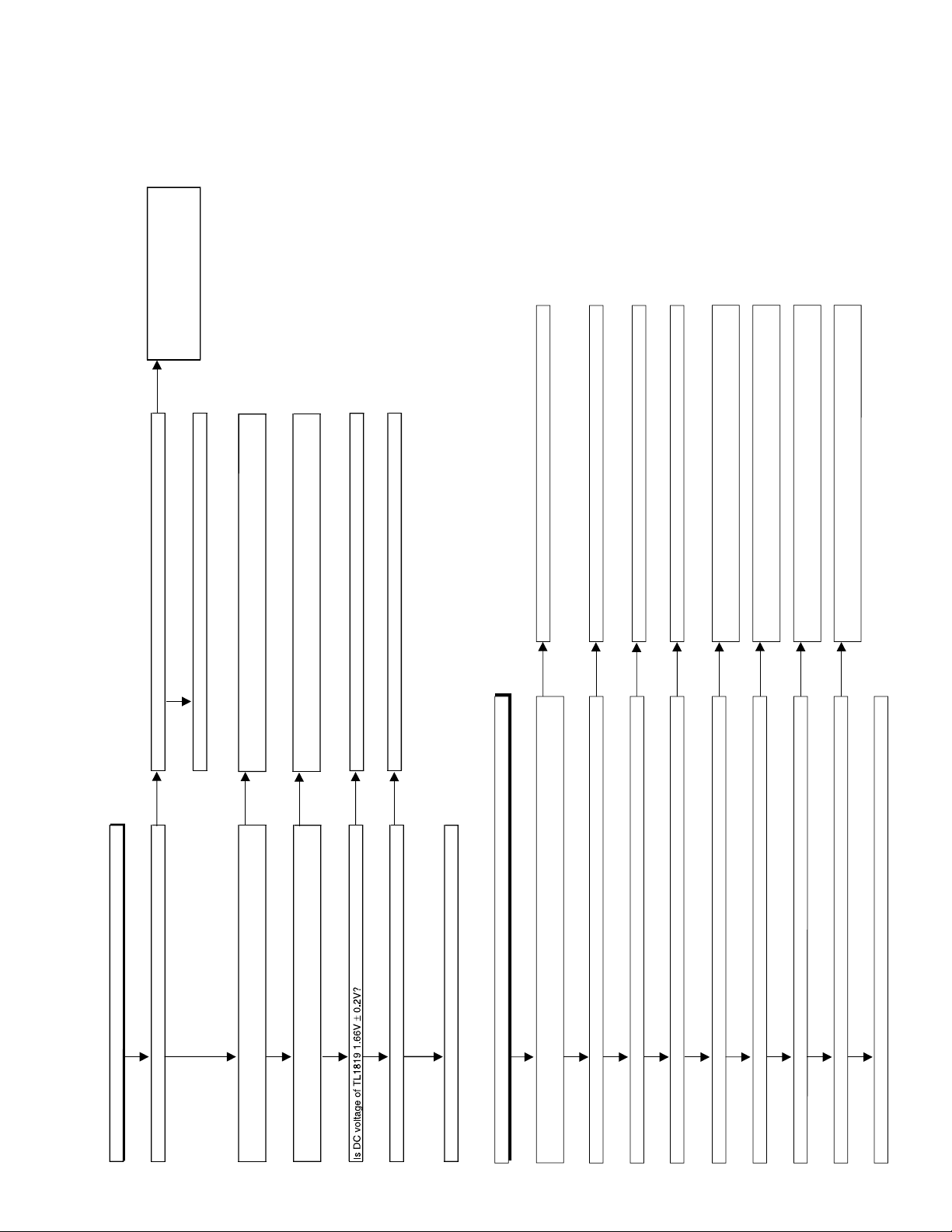
LCD PWB troubleshooting
Image is not displayed on LCD normally.
No
Is backlight lit? Is 12V applied to TL1801?
Yes
Is voltage of 12V and 3.3V applied to TL1807 and TL1806, respectively?
No
Backlight of LCD unit is defective.
Yes
No
Is RGB signal sent to TL1815, TL1816 and TL1817?
Is CSYNC signal sent to TL1813?
Refer to "Power circuit troubleshooting".
Check FFC between MAIN PWB and LCD PWB.
No
No
Check peripheral circuit of L1802.
Check IC1801 27PIN to 32PIN.
Check SC801 on MAIN PWB and its peripheral circuit.
Check FFC between MAIN PWB and LCD PWB.
Check FFC between MAIN PWB
and LCD PWB.
Check IC8901 on MAIN PWB and its
peripheral circuit.
Yes
Yes
Yes
Is LCD-RGB signal sent to TL1836, TL1837 and TL1838?
Yes
LCD unit is defective. Replace
No
Sound playback system troubleshooting, when audio signal is not sent from line out (CG40 only)
Insert SD card recording sound into the set, and play back file in playback mode.
No
Is 3.3V applied to both ends of L1602, L1603 and L1605?
Is 5V applied to both ends of L1604?
Refer to "Power circuit troubleshooting".
Yes
No
Check peripheral circuit of IC1604 and FL1601.
Yes
No
Are IC1602 13PIN and 14PIN set to "H"?
Is 4.096MHz sent to R1637?
Check IC702 48PIN and 49PIN and its peripheral circuit.
Yes
Is pulse sent to IC1602 9PIN?
No
Yes
No
Is audio signal sent to IC1603 15PIN?
Check peripheral circuit of IC1602 15PIN.
Check peripheral circuit of IC1603 15PIN.
Yes
No
Is audio signal sent to IC1603 13PIN?
Check peripheral circuit of IC1603 13PIN and 14PIN.
IC1603 1PIN: "H" at audio output
Yes
No
Is audio signal sent from IC1603 12PIN?
Check peripheral circuit of IC1603 12PIN.
IC1603 1PIN: "H" at audio output
Yes
Is audio signal sent to TL4406 on JACK PWB?
Check periphery of IC1602 and peripheral circuit of IC204.
Yes
Video/Audio cable is defective.
No
Check FFC between JACK PWB and MAIN PWB.
Check peripheral circuit of J4403.
VE-CG30U
VE-CG40U
21
Page 22

VE-CG30U
Sound playback system troubleshooting, when sound is not heard from speaker (CG40 only)
Set confirmation tone to ON using menu, and turn on power again.
No
Is 3.3V applied to both ends of L1602, L1603 and L1605?
Is 5V applied to both ends of L1604?
Refer to "Power circuit troubleshooting".
Yes
No
Check peripheral circuit of IC1604 and FL1601.
Yes
No
Are IC1602 13PIN and 14PIN set to "H"?
Is 4.096MHz sent to R1637?
Check IC702 48PIN and 49PIN and its peripheral circuit.
Yes
Is pulse sent to IC1602 9PIN?
No
Yes
No
Is audio signal sent to IC1603 15PIN?
Check peripheral circuit of IC1602 15PIN.
Check peripheral circuit of IC1603 15PIN.
Yes
No
Is audio signal sent to IC1603 13PIN?
Check peripheral circuit of IC1603 13PIN and 14PIN.
IC1603 1PIN: "H" at audio output
Yes
No
Is audio signal sent from IC1603 5PIN and 7PIN?
Check peripheral circuit of IC1603 2PIN to 11PIN.
Yes
Periphery of P1701 on operation PWB, FFC between operation PWB and MAIN PWB, and speaker
unit are defective.
Check periphery of IC1602 and peripheral circuit of IC204.
Sound recording system troubleshooting
Set mode SW to MOVIE.
No
Is 3.3V applied to both ends of L1602, L1603 and L1605?
Is 5V applied to both ends of L1604?
Refer to "Power circuit troubleshooting".
Yes
No
Check peripheral circuit of IC1604 and FL1601.
Yes
No
Are IC1602 13PIN and 14PIN set to "H"?
Is 4.096MHz sent to R1637?
Check IC702 48PIN and 49PIN and its peripheral circuit.
Yes
Is audio signal sent to IC1602 3PIN?
No
Yes
No
Is pulse sent from IC1602 8PIN?
Check peripheral circuit of P1602.
Yes
No
Is image recorded to SD card?
Check SD card and peripheral circuit of SC201.
Yes
IC204 is defective.
Check peripheral circuit of P1602.
Check IC1603 16PIN to 24PIN.
VE-CG40U
22
Page 23

- M E M O -
VE-CG30U
VE-CG40U
23
Page 24

VE-CG30U
VE-CG40U
VE-CG30U
VE-CG40U
7. BLOCK DIAGRAMS
7-1. GENERAL BLOCK DIAGRAM (VE-CG40U)
J
EXCLUSIVE
STROBE UNIT
KLMPWA002WJZZ
I
S
C
3
0
SHUT
TER
0
1
H
LED-T
LENS
PLNSAA004WJN1
G
PI
ZOOM
PI
MOTOR
SC1002SC1001
FOCUS[1:4]
ZOOM[1:4]
IG[1:4]
F
IC1001
LENS DRIVER
VHILB8 649FN-1Y
PH_VDD
E
D
Q1001
VSRT1P141U/-1Y
C
S204
ZOOM -TELE
B
S1702
LEFT
MACRO/T HUMBNAIL
A
S205
ZOOM -WIDE
S1701
UP
S1703
S1704
RIGHT
DOWN
S1706
MENU
S1707
FLASH/DELETE
OPERATION
DUNTKB358PM00
SC702
SC1701
S1708
ENTE R/DISP
S1705
S1709
EASY
P
1
7
0
1
IC8901
LED DRIVER
VHITK1 1850L-1Y
Q8901
VSRN1704///-1Y
ST_XON,ST_GSEL1,ST_GSEL2,ST_START,ST_FULL
OPE
LPF
VHLRJ21R3BA-1
FC_SENS,Z_SENS
BATT_NONR EG
FLASH,MACRO,MENU,ENTER,EASYPUP
SP+,SP-
VECG40U
DC-DC C ONVERTER
VHIMB3 9A102-1Y
IC1
CCD
4 Mega Pixels
ZOOM[0:3],FOCUS[0:3]
PHIR_O N
ZOOM
UP/DOWN,LEFT/RIGHT
D701
LED
R/G
H1,H2
V2,V4
V1A,V1B
V3A,V3B
VS2SC5383F/-1Y
Q711
VSRN4983///-1Y
ADC_SW
FL701
5MHz FILTER
RCRMC0001TAZZY
Q710
VSRN4983///-1Y
SPEAKER UNIT
PSP-ZA018WJZZ
BATTERY TEMP
DET UNIT
RUNTKA028WJZZ
IC1901
P-CON_H,DPCON_H
BL_CTRL
LEDT
CCDV CCD_VIDEO
Q1
BATT_V_DET
LED_GREEN
LED_RED
ST_GNO
VS2SC4627CD-1Y
IC2
TG V- DRIVER
VHILRS 5715+-1Q
OFDCOFD
SYS_3.3V
SYS_3.3V
BATT_CTRL
Q2
PBLX,BCPX,CLPX
ADCLK,SHD,SHP
SHUTTER[0:3],SPMCTRL
3.3V
IC701
SYSTEM RESET
VHIPST 3627U-1Y
RESETZ
8bit MIC R O COMPUTER
µPD78 0024A
RH-IXA 274WJZZQ
IC701
CDS/AGC/ADC
VHIVSP 2270M-1Q
BATT_TEM P
POW,MODE
TGVD,TGHD,CCDCLK
TGSCLK,TGSDATA,TGCS,TGID
BATT_TEMP_DET
BATT_TEMP
IC3
CDSCS,CDSDAT
CDSCLK
VHIMB8 346BV-1Y
RCRSCA039WJZZY
24MHz FILTER
RCRMCA010WJZZY
EXSDO
VPP,RESETZ,VDD
EXCK,EXSDI
POW,MODE
IC1201
DAC
X201
27MHz X'tal
FL201
BUSY,TGVD
UARTSI,UARTSO
UARTACK
USARTSI,USARTSO
USARTCK,USARTACK
SYS_RESET
SC701
Vers ionUP
Conector
P
7
2
0
1
CCDIN[2:11]
DACCS
SDATIRIS_CTRL1,IRIS_CTRL2
SCLK
CLK1I
CLK1O
CLK3I
CLK3O
TOP
DUNTKB360PM00
S1/S2
MODE
TXD
RXD,BOOT
POWER
SC7201
SC8201
S1,S2
CCD signal
proce sser 1
CCD signal
proce sser 2
ARM7TDMI
PLL
UART_0/1
USAR T_0/1
SP+,SP-
X2201
32kHz X'tal
RCRSC0032TAZZY
IC2201
RTC
VHIRS5 C313/-1Y
RTCCS
SDAT
SCLK
260p in BGA
CORE 1.8V
I/O 3.3V
GIO
IC1802
EEPROM
VHIBR9 3L46F-1Y
EEPROMCS,SDAT,SCLK
EEPROMDI
SDAT,SCLK,LCDCS
EEPROMDI
EEPROMCS
VIDEO ENCODE
LCD I/F
VREF_ADJ
VCO_ADJ
JPEG
RESIZE
AUDIO I/F
I C201
VHILR38668Y-1Q
USB 1.1 & DRIVER
MEDIA I/F
SD CAR D MEMORY
CONT ROLER
MEMORY CONTROLER
SDRAM
NOR FLASH
MEMUUDQM
MEMCASZ,MEMWEZ
MEMCS0Z,MEMRASZ
MUTE,EMPH
MEMD[0:15]
MEMA[0:13]
128M SDRAM
RH-IXA 124WJZZQ
Q2403
VSRT1P141U/-1Y
MEMA[0:13]
MEMD[16:31]
MEMCLK
MEMULDQM
IC2408
128M SDRAM
RH-IXA 124WJZZQ
VPP_ON
ADPON,DAPON
LCD I/F
DUNTKB514QA
IC1801
LCD TG
SIGNAL AMP
VHILRS 57191-1Q
SDAT,SCLK,LCDCS
CSYNC
LCDR
SC1802
SC801
CSYNC
BOUT
GOUT
SDPON SD_POWER
MEMCLK
MEMLLDQM
MEMLUDQM
MEMCASZ,MEMWEZ
MEMCS0Z,MEMRASZ
IC2403
SYS_RESETZ
LCDB
LCDG
LCDB
LCDG
LPF
LPF
ROUT
ASDO
ASDI
ASCLK,AXSYNCO
TCLK
SD_ENABLE
SDCLK
SDCSZ(DAT3)
SDDO(DAT0)
SDDIN(CMD)
SDCD
SDWP
VHIPQ1 X331M-1Y
MEMD[0:15]
MEMA[0:19]
IC2405
16M NOR FLASH
VHILHF 16J14-1Q
VPP
S
C
1
8
0
1
S
C
1
8
0
3
LCDR
LPF
SCLK,SDAT,CS_AUDIO
IC202
BUFFER
VHILVC 244T+-1Y
IC203
3.3V REG
SDCOVER
FL_EXOEZ
FLRP0Z,FLCE0Z
FLWPZ,FL_EXWEZ
LCD PANEL
SHAR P 1.5"
CG Silicon TFT
3LED BACKLIGHT
RLCUCA002WJZZ
CompositeVideo
IC1602
AUDIO CODEC
VHIPCM 3008+-1Y
IC1604
INVERTER
VHITC7 WU04F-1Y
USBP,USBM
IC401
VIDEO DRIVER
VHITK1 5417M-1Y
AOUT
AIN
RCRMC0004CEZZY
SDCLK
SDCSZ(DAT3)
SDDO(DAT0)
SDDIN(CMD)
S201
OVC ER SW
2002/07/03 12:44
CONFIDENTIAL
MIC
C-VIDEO
IC1603
AUDI O I/F
VHIBH6 406FV-1Y
DAPON,ADPON
FL1601
4.096MHz
SC201
SD CARD
SOCKET
QSOCZA 035WJZZY
SD
CARD
DUNTKB356QA
MIC
MAIN
P
1
6
RMICCA003WJZZ
0
2
S
AOUT
C
4
0
1
MIC UNIT
P4401
J4401
DC JACK
QJAKE0171CEZZ
S
C
4
J4403
4
AV-OU T JACK
0
QJAKE0060TAZZ
1
SC4402
USB PLUG
QJAKZ0078TAZZ
JAC
K
DUNTKB359PM00
1234567891011 12 13 14 15 16 17 18 19 20
24~25
Page 25

VE-CG30U
VE-CG40U
VE-CG30U
VE-CG40U
7-2. GENERAL BLOCK DIAGRAM (VE-CG30U)
J
I
H
G
F
E
D
C
B
A
EXCLUSIVE
STROBE UNIT
KLMPWA002WJZZ
LED-T
LENS
PLNSAA004WJN1
ZOOM
PI
MOTOR
FOCUS[1:4]
LENS DRIVER
VHILB8 649FN-1Y
PH_VDD
Q1001
VSRT1P 141U/-1Y
SC702
SC1701
S1703
RIGHT
S1708
ENTE R/DISP
S1705
FLASH /DELETE
S204
ZOOM -TELE
MACRO/T HUMBNAIL
S1702
LEFT
S1706
MENU
S1707
ZOOM -WIDE
S1701
UP
S1704
DOWN
PI
S205
OPERATION
DUNTKB358PM01
IC1001
S1709
EASY
ZOOM[1:4]
SHUT
TER
SC1002SC1001
IG[1:4]
S
C
3
0
0
1
VECG40U
IC8901
LED DRIVER
VHITK1 1850L-1Y
Q8901
VSRN17 04///-1Y
ST_XON,ST_GSEL1,ST_GSEL2,ST_START,ST_FULL
OPE
LPF
IC1
CCD
3 Mega Pixels
VHLRJ 21P3BA-1
VSRN49 83///-1Y
ZOOM[0:3],FOCUS[0:3]
PHIR_ON
FC_SENS,Z_SENS
RCRMC0 001TAZZY
BATT_NONREG
UP/DOWN,LEFT/RIGHT
FLASH,MACRO,MENU,ENTER,EASYPUP
ZOOM
VSRN49 83///-1Y
D701
LED
R/G
VS2SC5383F/-1Y
5MHz FILTER
Q710
BATTERY TEMP
DET UNIT
RUNTKA028WJZZ
IC1901
DC-DC C ONVERTER
VHIMB3 9A102-1Y
P-CON_H,DPCON_H
BL_CTRL
LEDT
CCDV CCD_VIDE O
H1,H2
V2,V4
V1A,V1B
V3A,V3B
Q1
Q711
ADC_SW
FL701
BATT_V_DET
LED_GREEN
LED_RED
ST_GNO
VS2SK508///-1Y
IC2
TG V- DRIVER
VHILRS 5714+-1Q
OFDCOFD
SYS_3.3V
SYS_3. 3V
BATT_CTR L
Q2
PBLX,BCPX,C LPX
ADCLK,SHD,SHP
SHUTTER[0:3],SPMCTRL
3.3V
IC701
SYSTEM RESET
VHIPST3627U-1Y
8bit MICR O COMPUTER
µPD78 0024A
RH-IXA 274WJZZQ
BATT_TEM P
RESETZ
IC701
CDS/A GC/ADC
VHIVSP2260M-1Q
POW,MODE
TGVD,TGHD,CCDCLK
TGSCLK,TGSDATA,TGCS,TGID
VPP,RESETZ, VDD
EXCK,EXSDI
BATT_TEMP_DET
BATT_TEMP
POW,MODE
IC3
CDSCS,CDSDAT
CDSCLK
IC1201
DAC
VHIMB8 346BV-1Y
X201
27MHz X'tal
RCRSCA039WJZZY
FL201
24MHz FILTER
RCRMCA010WJZZY
BUSY,TGVD
UARTSI,UARTSO
UARTACK
USARTSI,USARTSO
USARTCK,USARTACK
SYS_RESET
EXSDO
Vers ionUP
Conector
SC701
P
7
2
0
1
CCDIN[3:12]
DACCS
SDATIRIS_CTRL1,IRIS_CTRL2
SCLK
CLK1I
CLK1O
CLK3I
CLK3O
TOP
DUNTKB360PM00
S1/S2
MODE
TXD
RXD,BOOT
POWER
SC7201
SC8201
S1,S2
CCD signal
proce sser 1
CCD signal
proce sser 2
ARM7TDMI
PLL
UART_0/1
USAR T_0/1
RCRSC0032TAZZY
X2201
32kHz X'tal
IC2201
RTC
VHIRS5 C313/-1Y
RTCCS
SDAT
SCLK
260pin BGA
CORE 1.8V
I/O 3.3V
GIO
IC1802
EEPROM
VHIBR9 3L46F-1Y
EEPROMCS,SDAT,SCLK
EEPROMDI
SDAT,SCLK,LCDCS
EEPROMDI
EEPROMCS
VIDEO ENCODE
LCD I/F
VREF_ADJ
VCO_ADJ
JPEG
RESIZE
AUDIO I/F
I C201
VHILR38668Y-1Q
USB 1.1 & DRIVER
MEDIA I/F
SD CAR D MEMORY
CONTROLER
MEMORY CONTROLER
SDRAM
NOR FLASH
MEMUUDQM
MEMCASZ,MEMWEZ
MEMCS0Z,MEMRASZ
MEMD[0:15]
MEMA[0:13]
128M SDRAM
RH-IXA 124WJZZQ
Q2403
VSRT1P141U/-1Y
MEMA[0:13]
MEMD[16:31]
MEMCLK
MEMULDQM
IC2408
128M SDRAM
RH-IXA 124WJZZQ
VPP_ON
LCD I/F
DUNTKB514QA
IC1801
LCD TG
SIGNAL AMP
VHILRS 57191-1Q
SDAT,SCLK,LCDCS
CSYNC
LCDR
SC1802
SC801
CSYNC
BOUT
GOUT
SDPON SD_POWER
MEMCLK
MEMLLDQM
MEMLUDQM
MEMCASZ,MEMWEZ
MEMCS0Z,MEMRASZ
IC2403
LCDB
LCDG
LCDB
LPF
LPF
ROUT
SD_ENABLE
SDCLK
SDCSZ(DAT3)
SDDO(DAT0)
SDDIN(CMD)
SDCD
SDWP
VHIPQ1 X331M-1Y
MEMD[0:15]
MEMA[0:19]
IC2405
16M NOR FLASH
VHILHF 16J14-1Q
VPP
LCDG
LCDR
LPF
VHILVC 244T+-1Y
IC203
3.3V REG
SDCOVER
FL_EXOEZ
FLWPZ,FL_EXWEZ
S
C
1
8
LCD PANEL
0
SHAR P 1.5"
1
CG Sil icon TFT
3LED BACKLIGHT
S
C
RLCUCA 002WJZZ
1
8
0
3
CompositeVi deo
IC202
BUFFER
FLRP0Z,FLCE0Z
VIDEO DRIVER
VHITK1 5417M-1Y
USBP,USBM
SDCLK
SDCSZ(DAT3)
SDDO(DAT0)
SDDIN(CMD)
S201
OVC ER SW
IC401
2002/07/03 12:44
CONFIDENTIAL
C-VIDE O
SC201
SD CARD
SOCKET
QSOCZA035WJZZY
SD
CARD
MAIN
DUNTKB357QA
P4401
J4401
DC JACK
QJAKE0171CEZZ
S
S
C
C
4
4
V-OU T JACK
0
QJAKE0 060TAZZ
1
USB PLUG
QJAKZ0 078TAZZ
JAC
J4403
SC4402
K
4
0
1
DUNTKB359PM01
1234567891011 12 13 14 15 16 17 18 19 20
26~27
Page 26

VE-CG30U
(
)
(
)
VE-CG40U
VE-CG30U
VE-CG40U
7-3. POWER SECTION BLOCK DIAGRAM
J
I
H
G
F
E
D
AC ADAPTOR
OUT: 6.0V – 7.0V (planed)
Electric current rating
(not yet determined)
Size AA battery, 4 cells
Voltage: 4.0 – 7.2V
(1.0 - 1.8V per cell)
to SYSCON
DC JACK V_DET
BATT_V_DET
4CH Power control IC
EPR AMP
EPR AMP
EPR AMP
EPR AMP
OFF when the DC
jack is inserted
PWM
COMP
PWM
COMP
PWM
COMP
PWM
COMP
DC JACK
D1
DPCON_3.3V
FET2 APCON_3.3V 3.3 ± 0.15V
FET1 APCON_5V
Vf2 APCON_5V
Vf1 IO
5.5V booster circuit
5.5V
5.0V *1
REG circuit
5.0V
REG circuit
SP_5V *1
+
OFF when the voltage
—
N-ch FET
DRIVER
P-ch FET
DRIVER
P-ch FET
DRIVER
P-ch FET
DRIVER
is applied to the DC
input
3.5V dropper circuit
Composite
part adopted
1.8V dropper circuit
Composite
part adopted
Multi-transformer circuit
REG16V
3.3V
REG circuit
3.3V
RE
iri
DPCON_1.8V
12V
REG circuit
15V
*1: Only CG40 system for the AUDIO circuit and SP5V
APCON_5V
AM
V
CAM_ON
CAM3.3V
APCON_3.3V
LENS_3.5V
DPCON_3.3V
LCD 3.3V
LCD_ON
LCD 12V
CAM_15V
Line name
Connected to
DPCON_1.8V
Connected to
APCON_3.3V 3.3 ± 0.1V
Connected to
DPCON_3.3V 3.3 ± 0.3V
Connected to
DPCON_3.3V
SYS_3.3V
BATT_NONREG
Connected to
CAM_15V
CAM_-7V
CAM_5V
CAM_3.3V
Connected to
CAM_3.3V
LENS_3.5V 3.5 ±0..1V
Connected to
APCON_5V
APCON_3.3V
SP_5V 5.5 ± 0.3V
Connected to
LCD_12V
LCD_3.3V
Connected to
NONREG
APCON_5V 5.0 ± 0.1V
Required spec
ASIC
1.8 ± 0.1V
4.9 ± 0.1V
3.3 ± 0.15V
5.0 ± 0.1V
MEM
SYSCON
3.3 ± 0.1V
3.3 ± 0.1V
7.5V
3.6
CCD
15.0 ± 0.4V
-7.0 ± 0.3V
5.0 ± 0.1V
3.3 ± 0.1V
LENS
3.3 ± 0.1V
AUDIO *1
5.0 ± 0.3V
3.3 ± 0.3V
LCD
12.0 ± 0.4V
3.3 ± 0.1V
STROBE
7.5V
3.6
REG circuit
CAM_ON
REG-8V
CAM-7V
CAM 7V
REG circuit
Table 1. Operation of each section and the D/D converter input voltage by
C
plugging/unplugging the DC jack
Operation mode
Plugging/
unplugging the jack
DC voltage
FET1 ON OFF OFF OFF ON
B
FET2 ON
D/D IN
Vf2: parasitic diode Vf2 of FET2 which is one of two FETs
BATT operation
Batt BattBatt-Vf2 Batt-Vf2DC output
Plugging
ON OFF ON ON
Adaptor
operation
Unplugging
BATT operation
Constant current circuit for white LED
SYS3.3V REG circuit
(MM3033)
SYS 3.3V
White LED unit
10.3V (3 lights), 15mA
Sub-microcomputer
RTC
A
1234567891011 12 13 14 15 16 17 18 19 20
28~29
Page 27

VE-CG30U
60
SIC
CC
(
(
( A)
( A)
( B)
(
(
)
SC
Z
Z
QPLG
S
5
6
3
VE-CG40U
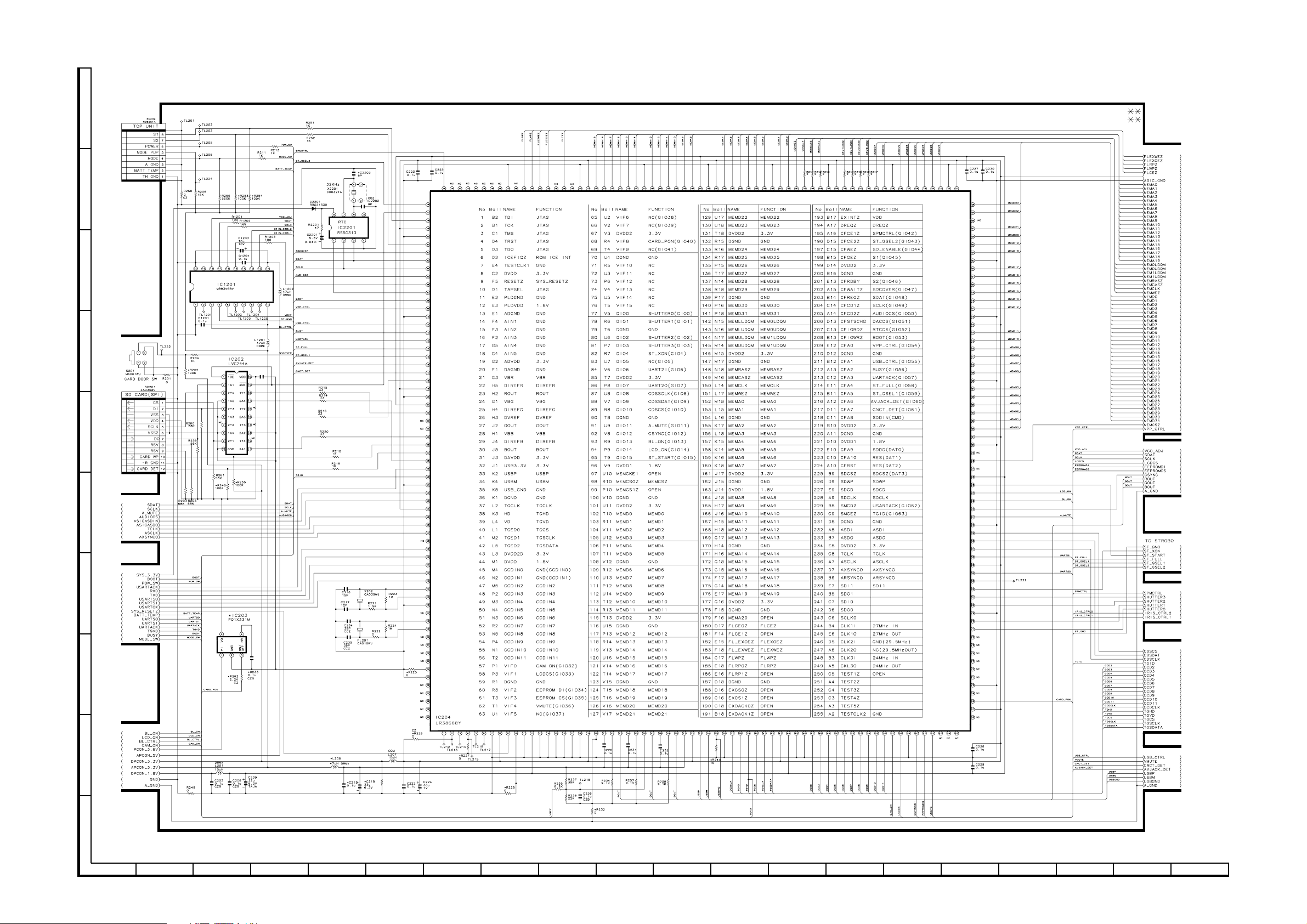
8. SCHEMATIC DIAGRAMS
8-1. OVERALL SCHEMATIC DIAGRAM (VE-CG40U)
J
MIC
RMICCA003WJZZ
I
LENS
H
FOCUS
RESET
ZOOM
FPC
M
G
FOCUS
M
F
IRIS
E
USB
VBUS 1 USBM 10 10 USBM IO POWER 4 12 ST XON
D - 2 USBGND 9 9 USBGND 5 11 ST MODE
D + 3 USBP 8 8 USBP 6 10 P CON5
4 VBUS 7 7 VBUS 7 9 GND
GND
AV
D
1
3
2
DC IN
C
JACK
DUNTKB359PM
QPWBNB359WJ
M
AV JACK DET. 6 6 AV JACK DET. 8 8 GND
AVGND 5 5 AVGND 9 7 GND
AUDIO OUT 4 4 AUDIO OUT 10 6 ST-DET
AVGND 3 3 AVGND 11 5 ST- CHRG
VIDEO OUT 2 2 VIDEO OUT 12 4 TALLY LED
DC JACK DET. 1 1 DC JACK DET. 13 3 NONREG
SC4401 SC401 14 2 NONREG
QSOCN1072TAZZY QSOCN1007REN1Y 15 1 NONREG
DC IN DC IN
DC IN DC IN
GND GND
GND
P4401 P2901
QPLGN0463TAZZY QPLGN0458REZZY GND 1
B
1 MIC
2 GND A
2
P1
QPLGN0274TAZZ
CCD
TG
V-DRIVER
SC1001 LENS 4
QSOCN1672TAZZY
16 NC 2
15 SENS (FOCUS)
14 VCC LB8649FN P7201
13 IRED QPLGN0276TAZZY
12 ZOOM 4
11 ZOOM 2
10 ZOOM 1
9 ZOOM 3 QSOCZA035WJZZY
8 FOCUS 1
7 FOCUS 3
6 FOCUS 2
5 FOCUS 4
4 SENS VDD 4
3 VCC SCLK 5
2 IRED VSS2 6
1NC DO 7
FPC
6NC COVER GND 11
5 IG 4 DET. CARD 12
4 IG 2
3 IG 3
2 IG 1 P3001
1NC
FFC
4
1
3
2
2
3
1
4
WIRE HARNESS
QCNW-A565WJZZ
(FOCUS)
(FOCUS)
/B) 2 TH GND
/A) 1 BATT TEMP
( B)
CS 1
/A) DI 2
/B
(ZOOM)
(ZOOM)
(ZOOM)
SC1002 RSV 9
QSOCN0672TAZZY CARTE WP 10
QCNW-A562WJZZ
GND
AUDIO
CG40 MAIN
DUNTKB356PM
QMPWCB356WJ
D
CDS/ADC
32KHz
EEPROMC
SCLK
SCLK
EEPROMC
PCTL
PCTLB
3 4 5 61 2
LCDCS
LCDCS
P VID
1 2
Quartz
SDAT
SDAT
VRVGVB
49MHz Quartz
LENS DRIVER 1
ZOOM DRV
AF DRV
SHUTTER DRV
LED GND
LED GND
123456789101112131415161718
123456789101112131415161718
LED GND
LED GND
SC1803 QSOCN0672TAZZ QSOCN2472TAZ
LED GND
LED GND
LED 12V
LED 12V
LED GND
3 4 5 61 2
1 2
GND
LED 12V
GND
LED 12V
LED 12V
LED 12V
LCD 3.3V
LCD 12V
LCD 12V
LCD 3.3V
LED 12V
EEPROMD1
EEPROMD1
TCOM
CSYNC
CSYNC
4
27MHz
Quartz
24MHz
Quartz
VCO ADJ
R SIG
R SIG
VCO ADJ
VDD (12V)
RTC
G SIG
G SIG
SCK
7
B SIG
B SIG
SCKB
11 12 137 8 9 10
GND
FFC
GND
SSP
VSS (0V)
QSOCN1872TAZ
SSPB
A
ASIC
LR38668Y
SC801
QSOCN1898TAZZY
QCNW-A566WJZZ
1802
GVDD
INI
INI
GSP
GSK1
SC1801
GSK2UDLR
20 21 22 2314 15 16
CGS LCD
VREF
ADOUT (NC)
GDOUT (NC)
2417 18
MENU
MEM
Sub µ-COM
SC702
SC1701
ENTER
QSOCN1098AZZY
GND A
MENU
ENTER
FLASH
MACRO
UP/DOWN
MACRO
LEFT
LEFT/RIGHT
UP/DOWN
LEFT/RIGHT
1 2 3 4 5 6 7 8 9 10
10 9 8 7 6 5 4 3 2 1
MENU
GND A
ENTER
FLASH
QSOCN1025TAN1
FLASH
MACRO
POWER
EASY PUP
SP –
SP –
EASY PUP
UP
DOWN
SC201
SD
CARD SOCKET
SP +
QCNW-A563WJZZ
FFC
OPERATION
SP +
DUNTKB358PM
QPWBNB359WJ
RIGHT
EASY
POP UP
N0276TAZZY
8
7
6
5
3
MODE
S 1S 1
S 2S 2
POWERPOWER
MODE PUPMODE PUP
MODEMODE
A GND
BATT. TEMP.BATT. TEMP.
TH GNDTH GND
SHUTTER
ZOOM
TW
SC202 SC7201
QCNW-A561WJZZ
QSOCN0825TAN1Y QSOCN0871TAZZY
A GND
FFC
TOP - OPERATION
DUNTKB360PM
QPWBNB360WJ
VSS 3
RSV 8
QCNW-A564WJZZ
QSOCN1507REN1Y
P2902
QPLGN0463TAZZY
P1701
SP + 1
SP - 2
ST GNO
ST GSEL1
ST GSEL2
ST XON
ST MODE
P CON5
GND
GND
GND
ST-DET
ST- CHRG
TALLY LED
NONREG
NONREG
NONREG
BATT IN
BATT IN
GND
SPEAKER
FFC
1 15 ST GNO
2 14 ST GSEL1
3 13 ST GSEL2
4
3
2
QSOCN1571TAZZY
QTANZA006WJZZ
QTANZA007WJZZ
V
PA016P-F18N
KLMPWA002WJZZ
STROBE
POWER
TEMP. DET.
RUNTKA028WJZZ
VE-CG30U
VE-CG40U
A
1234567891011 12 13 14 15 16 17 18 19 20
30~31
Page 28

VE-CG30U
SIC
CC
(
(
( A)
( A)
( B)
(
(
)
SC
Z
Z
QPLG
VE-CG40U
VE-CG30U
VE-CG40U
8-2. OVERALL SCHEMATIC DIAGRAM (VE-CG30U)
J
MODE
SHUTTER
8
S 1S 1
7
S 2S 2
6
POWERPOWER
5
MODE PUPMODE PUP
MODEMODE
3
A GND
BATT. TEMP.BATT. TEMP.
TH GNDTH GND
TOP - OPERATION
DUNTKB360PM
QPWBNB360WJ
QCNW-A564WJZZ
QSOCN1571TAZZY
STROBE
KLMPWA002WJZZ
POWER
TEMP. DET.
RUNTKA028WJZZ
A
ASIC
LR38668Y
INI
GSP
CG40 MAIN
DUNTKB356PM
QMPWCB356WJ
SC1801
GSK2UDLR
GSK1
20 21 22 2314 15 16
ADOUT (NC)
VREF
GDOUT (NC)
2417 18
MENU
MEM
Sub µ-COM
SC702
SC1701
ENTER
QSOCN1098AZZY
GND A
MENU
ENTER
FLASH
MACRO
UP/DOWN
MACRO
LEFT
LEFT/RIGHT
UP/DOWN
LEFT/RIGHT
1 2 3 4 5 6 7 8 9 10
10 9 8 7 6 5 4 3 2 1
MENU
GND A
ENTER
FLASH
QSOCN1025TAN1
FLASH
MACRO
POWER
EASY PUP
EASY PUP
UP
DOWN
SC201
SD
CARD SOCKET
FFC
OPERATION
DUNTKB358PM
QPWBNB359WJ
RIGHT
EASY
POP UP
N0276TAZZY
AUDIO
I
CCD
LENS
TG
FOCUS
H
G
RESET
ZOOM
FOCUS
F
IRIS
USB
E
D
VBUS 1 USBM 10 10 USBM IO POWER 4 12 ST XON
D - 2 USBGND 9 9 USBGND 5 11 ST MODE
D + 3 USBP 8 8 USBP 6 10 P CON5
4 VBUS 7 7 VBUS 7 9 GND
GND
AV
DC IN
DUNTKB359PM
QPWBNB359WJ
1
3
2
JACK
AV JACK DET. 6 6 AV JACK DET. 8 8 GND
DC JACK DET. 1 1 DC JACK DET. 13 3 NONREG
SC4401 SC401 14 2 NONREG
QSOCN1072TAZZY QSOCN1007REN1Y 15 1 NONREG
P4401 P2901
QPLGN0463TAZZY QPLGN0458REZZY GND 1
FPC
M
M
FPC
M
FFC
AVGND 5 5 AVGND 9 7 GND
AUDIO OUT 4 4 AUDIO OUT 10 6 ST-DET
AVGND 3 3 AVGND 11 5 ST- CHRG
VIDEO OUT 2 2 VIDEO OUT 12 4 TALLY LED
DC IN DC IN
DC IN DC IN
GND GND
GND
1
2
3
4
QCNW-A565WJZZ
V-DRIVER
SC1001 LENS 4
QSOCN1672TAZZY
16 NC 2
15 SENS (FOCUS)
14 VCC LB8649FN P7201
13 IRED QPLGN0276TAZZY
12 ZOOM 4
11 ZOOM 2
10 ZOOM 1
9 ZOOM 3 QSOCZA035WJZZY
8 FOCUS 1
7 FOCUS 3
6 FOCUS 2
5 FOCUS 4
4 SENS VDD 4
3 VCC SCLK 5
2 IRED VSS2 6
1NC DO 7
6NC COVER GND 11
5IG 4 DET. CARD 12
4IG 2
3IG 3
2IG 1 P3001
1NC
4
3
2
1
WIRE HARNESS
(FOCUS)
(FOCUS)
/B) 2 TH GND
/A) 1 BATT TEMP
( B)
CS 1
/A) DI 2
/B
(ZOOM)
(ZOOM)
(ZOOM)
SC1002 RSV 9
QSOCN0672TAZZY CARTE WP 10
QCNW-A562WJZZ
GND
C
B
D
CDS/ADC
32KHz
EEPROMC
SCLK
SCLK
EEPROMC
PCTL
PCTLB
3 4 5 61 2
X'tal
LCDCS
LCDCS
P VID
1 2
SDAT
SDAT
VRVGVB
49MHz X'tal
LENS DRIVER 1
ZOOM DRV
AF DRV
SHUTTER DRV
LED GND
LED GND
123456789101112131415161718
123456789101112131415161718
LED GND
LED GND
SC1803 QSOCN0672TAZZ QSOCN2472TAZ
LED GND
LED GND
LED 12V
LED 12V
LED GND
3 4 5 61 2
LED 12V
LED 12V
LED 12V
1 2
GND
LCD 3.3V
GND
LCD 3.3V
LED 12V
LED 12V
LCD 12V
LCD 12V
TCOM
EEPROMD1
EEPROMD1
CSYNC
CSYNC
4
27MHz
X'tal
24MHz
VCO ADJ
R SIG
R SIG
VCO ADJ
VDD (12V)
X'tal
RTC
G SIG
G SIG
SCK
7
B SIG
B SIG
SCKB
11 12 137 8 9 10
GND
FFC
GND
SSP
VSS (0V)
SC801
QSOCN1898TAZZY
QCNW-A566WJZZ
1802
QSOCN1872TAZ
GVDD
INI
SSPB
CGS LCD
ZOOM
TW
SC202 SC7201
QCNW-A561WJZZ
QSOCN0825TAN1Y QSOCN0871TAZZY
A GND
VSS 3
RSV 8
QSOCN1507REN1Y
P2902
QPLGN0463TAZZY
ST GNO
ST GSEL1
ST GSEL2
ST XON
ST MODE
P CON5
GND
GND
GND
ST-DET
ST- CHRG
TALLY LED
NONREG
NONREG
NONREG
BATT IN
BATT IN
GND
FFC
FFC
1 15 ST GNO
2 14 ST GSEL1
3 13 ST GSEL2
4
3
2
QCNW-A563WJZZ
QTANZA006WJZZ
QTANZA007WJZZ
A
1234567891011 12 13 14 15 16 17 18 19 20
32~33
Page 29
VE-CG30U
VE-CG40U
VE-CG30U
VE-CG40U
8-3. ASIC SHEMATIC DIAGRAM
J
I
H
G
F
E
D
C
B
A
1234567891011 12 13 14 15 16 17 18 19 20
34~35
Page 30

VE-CG30U
VE-CG40U
VE-CG30U
VE-CG40U
8-4. I/O SCHEMATIC DIAGRAM
J
I
H
G
F
E
D
C
B
A
1234567891011 12 13 14 15 16 17 18 19 20
36~37
Page 31

VE-CG30U
VE-CG40U
VE-CG30U
VE-CG40U
8-5. SYSTEM CONTROL SCHEMATIC DIAGRAMS
J
I
H
G
F
E
D
C
B
A
1234567891011 12 13 14 15 16 17 18 19 20
38~39
Page 32

VE-CG30U
VE-CG40U
VE-CG30U
VE-CG40U
8-6. LCD I/F SCHEMATIC DIAGRAM
J
I
H
G
F
E
D
C
B
A
1234567891011 12 13 14 15 16 17 18 19 20
40~41
Page 33

VE-CG30U
VE-CG40U
VE-CG30U
VE-CG40U
8-7. LENS SCHEMATIC DIAGRAM
J
I
H
G
F
E
D
C
B
A
1234567891011 12 13 14 15 16 17 18 19 20
42~43
Page 34

VE-CG30U
VE-CG40U
VE-CG30U
VE-CG40U
å AND SHADED COMPONENTS=SAFETY RELATED PARTS
8-8. POWER SCHEMATIC DIAGRAM (VE-CG40U)
J
å
I
å
H
G
F
E
D
C
å
B
A
1234567891011 12 13 14 15 16 17 18 19 20
44~45
Page 35

VE-CG30U
VE-CG40U
VE-CG30U
VE-CG40U
å AND SHADED COMPONENTS=SAFETY RELATED PARTS
8-9. POWER SCHEMATIC DIAGRAM (VE-CG30U)
J
å
I
å
H
G
F
E
D
C
å
B
A
1234567891011 12 13 14 15 16 17 18 19 20
46~47
Page 36

VE-CG30U
VE-CG40U
VE-CG30U
VE-CG40U
8-10. MEM SCHEMATIC DIAGRAM
J
I
H
G
F
E
D
C
B
A
1234567891011 12 13 14 15 16 17 18 19 20
48~49
Page 37

VE-CG30U
VE-CG40U
VE-CG30U
VE-CG40U
8-11. STROBE I/F SCHEMATIC DIAGRAM
J
I
H
G
F
E
D
C
B
A
1234567891011 12 13 14 15 16 17 18 19 20
50~51
Page 38

VE-CG30U
VE-CG40U
VE-CG30U
VE-CG40U
8-12. CCD SCHEMATIC DIAGRAM (VE-CG40U)
J
I
H
G
F
E
D
C
B
A
1234567891011 12 13 14 15 16 17 18 19 20
52~53
Page 39
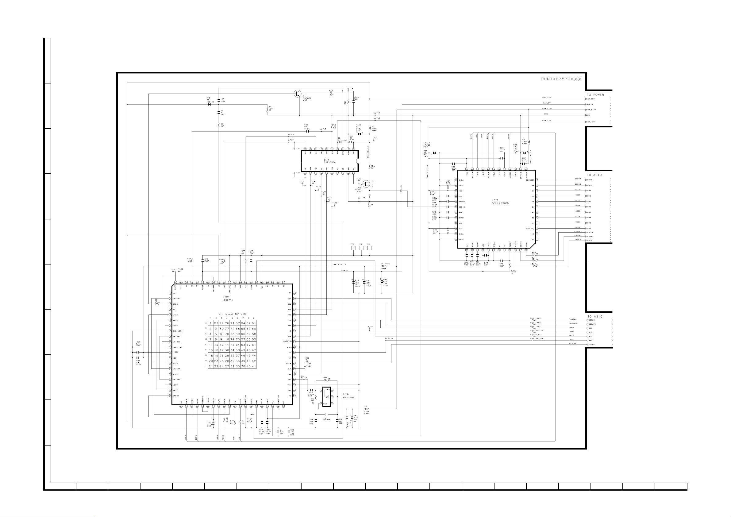
VE-CG30U
VE-CG40U
VE-CG30U
VE-CG40U
8-13. CCD SCHEMATIC DIAGRAM (VE-CG30U)
J
I
H
G
F
E
D
C
B
A
1234567891011 12 13 14 15 16 17 18 19 20
54~55
Page 40

VE-CG30U
VE-CG40U
8-14. AUDIO SCHEMATIC DIAGRAM (VE-CG40U)
J
I
H
G
F
E
D
C
B
A
12345678910
56
Page 41

8-15. OPERATION SCHEMATIC DIAGRAM (VE-CG40U)
J
I
H
VE-CG30U
VE-CG40U
G
F
E
D
C
B
A
10 11 12 13 14 15 16 17 18 19
12345678910
57
Page 42

VE-CG30U
VE-CG40U
8-16. OPERATION SHCMATIC DIAGRAM (VE-CG30U)
J
I
H
G
F
E
D
C
B
A
12345678910
58
Page 43

8-17. JACK SCHEMATIC DIAGRAM (VE-CG40U)
J
I
H
VE-CG30U
VE-CG40U
G
F
E
D
C
B
A
10 11 12 13 14 15 16 17 18 19
12345678910
59
Page 44

VE-CG30U
VE-CG40U
8-18. JACK SCHEMATIC DIAGRAM (VE-CG30U)
J
I
H
G
F
E
D
C
B
A
12345678910
60
Page 45

8-19. TOP-OPERATION SCHEMATIC DIAGRAM
J
I
H
VE-CG30U
VE-CG40U
G
F
E
D
C
B
A
12345678910
10 11 12 13 14 15 16 17 18 19
61
Page 46

VE-CG30U
VE-CG40U
VE-CG30U
VE-CG40U
8-20. LCD SIGNAL PROCESSOR / TIMING GENERATOR
J
I
H
G
F
E
D
C
B
A
1234567891011 12 13 14 15 16 17 18 19 20
62~63
Page 47

VE-CG30U
(
)
(
)
(
)
)
(
)
LRS5719
XXXX
VE-CG40U
9. SEMICONDUCTOR LEAD IDENTIFICATION
J
8
1
I
RH-iXA124WJZZQ(54pin)
VHiBH6406FV-1Y
VHiLVC244T+-1Y
VHiMB39A102-1Y
28pin
20pin
30pin
VHiMB8346BV-1Y(20pin
VHiPCM3008+-1Y
16pin
CHiLHF16J14-3 (48 ball)
CHiLHF16J14-4 (48 ball)
VHiLR38668Y-1Q (260 ball)
VHiLRS5714+-1Q (81 ball)
VHiLRS5715+-1Q (81 ball)
VHiRS5C313/-1Y
VHiSN2GU04C-1Y
VHiTK11851L-1Y
VSSi6967DQ+-1Y
VHiBR93L46F-1Y
5
4
1
H
33
48
49
G
64
32
36
17
16
1
37
(64pin)
RH-iXA274WJZZQ
VHiLB8649FN-1Y (48 pin)
24
25
13
37
VSP
12
48
1pin
YMLLLLS
48
1pin
VHiVSP2260M-1Y
2536
XXXXM
12
24
49
LRS5719
SHARP
XXXX
13
64
1pin
VHiLRS57191-1Q
3348
32
17
16
VHiVSP2270M-1Y
F
A
3
2
4
3
C
E
RH-EX1257CEZZY
RH-EX1273CEZZY
VHiMM3033D+-1Y
VHiPST3627U-1Y
2
1
VSMCH3405++-1Y
2
1
VHD1SS400++-1Y
VHDFS1J3///-1Y
VHDRB521S30-1Y
RH-EX1239CEZZY
VHDHVU17TRF-1Y
D
1
2
3
6
C
5
4
VHiTK15417M-1Y
VSFDG312P++-1Y
VSHN1A02F++-1Y
VSRN4982///-1Y
VSRN4983///-1Y
VSRN4984///-1Y
B
VSSi3853DV+-1Y
C
E
B
VS2SA1362GR-1Y
VS2SA1989R/-1Y
VS2SC4627CD-1Y
VS2SC5383F/-1Y
VSDTA114EE/-1Y
VSKTA2014EY-1Y
VSDTC114EE/-1Y
1
2
3
5
4
VHiPQ1X331M-1Y
VHiPQ1X501M-1Y
VHiSN1GU04C-1Y
VSKTC601UY+-1Y
VSRN1704///-1Y
D
S
G
VS2SK508///-1Y
VSHN1B04FU/-1Y
A
12345678910
64
Page 48

- M E M O -
VE-CG30U
VE-CG40U
10 11 12 13 14 15 16 17 18 19
65
Page 49
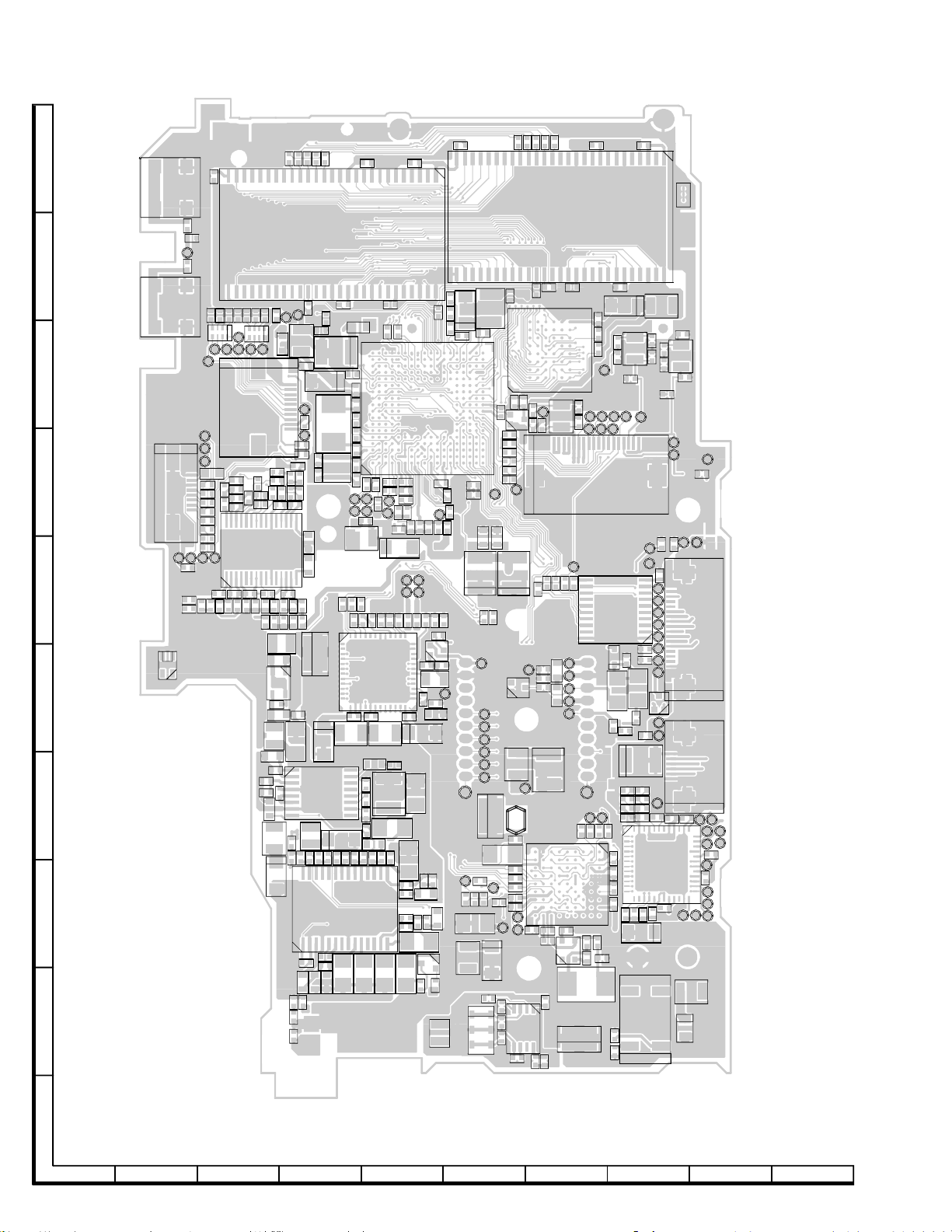
VE-CG30U
VE-CG40U
10. PRINTED WIRING BOARD ASSEMBLIES
C2416
J
S204
C2426
R2448
R2447
R2446
R2445
R2443
C2423 C2422
R2425
R2424
R2423
R2422
R2420
C2413 C2410
Z1
IC2403
R773
C715
TL771
I
S205
R772
TL715
TL766
C713
R767
TL713
C712
C711
TL709
C710
TL706
TL710
C709
R766
C708
TL705
C714
H
SC702
TL205
TL206
TL770
TH701
D701
SC202
TL224
R250
R763
R764
R211
R256
R206
R213
R253
R252
R254
R251
TL202
R1929
TL203
C1904
R1908
C1906
G
F
E
D
R1927
R1921
C1910
R1912
C1911 R1919
R1910
R1909
R1902
R1922
C1905
R1924
C1913
R1904
R6901
IC1901
R1903
C1901
C1608
R1611
R1914
R1915
R1926 R1906
L1601
C1603
R1613
C1610
C1611
R5901
R1916
C1605
C1614
C1902 R1905
L1602
L1604
C
B
TL6901
R720
TL707
R249
R1920
R1918
R1925
R1917
R1913
R1911
C1903 R1923
IC1601
R1602
C1607
R1609
R1630
C1646
C206
TL769
TL768
C718
FB702
R1907 C1907
C1606
R1635
R1601 R9904 R1603
L201
FB701
R1928
C1909
R1930 R1901
IC1602
C1624
R408 C1640
C2431
C1908 C1912
R1625
C203
C209
C235 C234
TP1
L1603
C1623
C1644
C1645
C1634
IC2408
C2424
R2444
C2419
X202
FL201
C36
C1617
R1624
C1619
IC1603
C1639
C223
TL212
TL213
R20
L5
C1618
C1638
R2410
C37
L206
R21
R222 R224 C216 R223 R221 C217 C225
TL215
TL214
C35
C1625
C215
R22
R19
C1622
R1619
R225
C30
C1613
C1601 R1638 C1602
R1618
C1637
R226
C34
IC3
C1631
R229
R228
TL217
R227
TL216
C33
L4
C1628
R1623
C2421
R242
R1615
C1636
R232
C218
C32
C1630
R1621
R244
R233
R234
R257
C226
TL8901
TL8903
C31
C1632
R1622
R1627
R1626
C231
FB8902
C22
C1635
R258
TL8904
TL8902
FB8901
C21
C1629
C1627
C1633
IC204
C236
C45
C23
C1621
C1641
Q1601
R1628
R236
C29
C26
C25
C1616
R1629
C227
TL218
R6
Q2
C24
R1617
R241
R237
C28
R7
TL15
C1643
R1640
L1605
TL808
IC4
TP3
C1204
TL23
R809 C801
R8
TL801
TL802
X1
TL803
TL804
SC801
TL6
TL7
R17
R39
R13
C14
C15
R2426 R2401 C2411
TL818
TL806
R16
C2409
C2408
R803 R806
TL807
TL805
IC1201
D1
C1
C7
R5
R1002
R1004
R1003
C1004
R18
C16 C17 C18 R12
C2203 C2202
R811
C1002
R2
C1001
L802
TL815
TL1015
TL1016
R1015
R1014
C2
R1
R9905
R1001
R1006
R1005
C1005
C1003
C19
C1007
X2201
L2404
C805 C802
TL1205
TL1204
TL1203
TL1202
TL1201
TL1006
TL1004
TL1005
TL1024
TL1025
TL1022
C1006
IC1001
C1010
C1008
R813
R1012
C1201
Q1001
C1009
R804 R807
TL816
TL814
TL1011
C803
TL1017
R1013
L803
C806
C1011
TL1013
L6
C41
TL817
R801
TL1023
SC1001
SC1002
TL1007
TL1008
TL1009
R1011
TL1019
TL1021
TL1014
TL1012
R1010
TL1010
TL1018
TL1020
C2414
R2421
C2430
C221
L207
C224
R243 R245 R246
C222
R247
IC2405
R2403
C2429
TL819
C229
Q2403
R834
R835
R837
R839
R836
R838
C228
TL823
TL222
C230
C232
R235 R240
C27
TL22
TL17
R270
R9907
C44
C46
R38
R36
TL14
TL13
TL12
TL11
TL10
TL9
TL8
TP2
C8
C9
R9
R11
R37
TL18
R10
C10
R33
R34
R35
R15
C11
TL20
C12
TL5902
TL19
L3
C20
R1637
R1631 R1636
FL1601
R1632
R1639
TL7902
Q1
L1
TL5901
IC1604
L801
R802 R805
C804
R1203
R1202
R1201
R840
TL1
C3
C5
TL2
R4
R3
TL4
C6
TL3
TL5
C4
IC2
C13
R14
C39
C40
R1633
C1651
C1652
A
MAIN PWB (VE-CG40U) SIDE A
12345678910
66
Page 50

VE-CG30U
VE-CG40U
C1202
TL4901
R4906
NTL2
L1201
L1202
Q3902
TL4902
R3904
C3904
C4906
R203
C4908 C3905
Q4903
IC3902
IC4902
R733
C706
Q710
R737
R4908
FL701
C705
C717
C716
R701
R715
R735
R734
R706
R740
R768
R736
R708 R709
R738
R775
R260
Q3903
R4904 R3903
R261
C4904
Q5908
R5905
IC703
IC4901
R4903
C5906
C704
C702
C4903
C703
R5911
C5910
R710
IC702
R725
SC201
R220
IC202
R216
Q5907
IC701
R215
R214
R5912
TL5903
R5910
R5913
C701
C7901
TL5904
R259
R5914
IC7901
C2204
Q5903
R7901
R7902
R771
R205
Q5904
C707
R762
R765
Q711
C7902
C5908
R769
R774
IC203
R5907
R5904
R262 C233
R5906
Q5905
C5909
C5907
R3901
C5902
R201
Q3901
D5902
C5904
R248 R219
R5909
C5913
R5908
R255
C3901
C5905
D5903
Q5906
R218
D5901
L5902
R5903
R2902
Q5902
S201
TL2911
R2901
IC2901
L3901
T5901
C5903
L5901
C5911
C43
D8901
R3902
C4907
R2904
R2903
L4902
R204 R202
L8901
TL223
TL2902
TL2906
TL2904
FB2902
D3901
R5902
L4901
F2902
R1616
R1620
C1642
TL2903
TL2905
Q5901
C5901
C1620
FB2901
TL2901
C6903
C1626
R8906
C3902
C6902
TL1628
C1604
FB1601
L6902
TL1627
Q6901
L6901
Q4901
C4902
L1901
FB1602
P2902
P1602
C4901
R6902
C6901
R4901
R4902
TL2907
TL2909
SC701
C1203
IC1
TL3002
C47
R2201
D2201
C42
TL7901
C2201
IC2201
TL3011
TL3013
TL3007
TL3010
TL3008
TL3004
TL3005
TL3006
TL3012
TL3901
SC3001
TL3009
C402 L401
R9902 R9903
MAIN PWB (VE-CG40U) SIDE B
C3001
R414
R401
C401
C48
TL3001
TL3003
IC401
C408
C404
C407
R9906
TL402
R403
D2902
F2901
Q401
R410
TL2908
TL2910
TL406
TL407
R409
C410
R402 R407
R8901
R8903
R8902
C406
C405
TL409
TL403
C409
R405
R404
R406
TL410
TL411
R411
C8901
TL405
TL404
TL408
P2901
C8902
IC8901
R8904
SC401
R3908
C3903
C8903
R8905
IC3901
C3906
10 11 12 13 14 15 16 17 18 19
67
Page 51

VE-CG30U
VE-CG40U
J
S204
C2426
R2448
R2447
R2446
R2445
R2443
C2416
C2423 C2422
R2425
R2424
R2423
I
TL6901
TL707
R720
R249
R1920
R1917
R1925R1918
R1913
R1911
C1903 R1923
L1601
IC1601
R1602
C1607
R1609
R1630
C1646
TL769
TL768
C718
FB702
R1907 C1907
C1606
R1635
R1603
R9904
R1601
C2431
L201
C206
FB701
C1909R1928
C1908 C1912
R1930 R1901
C1624
C1640
R408
IC2408
R2444
C203
C209
C235 C234
TP1
C36
IC1602
L1603
R1625
C1623
C1644
C1645
C1634
C2419
X202
R1624
C1639
C2424
R2410
C223
FL201
TL212
TL213
R21
R20
C35
C37
L5
C1617
C1618
C1619
IC1603
C1638
R222 R224 C216 R223 R221 C217 C225
TL215
TL214
C215
L206
C1625
R225
R22
R19
C30
C1613
C1601R1638C1602
R1618
C1622
R1619
C1637
C34
IC3
C1631
R226
TL216
C2421
R229
R228
TL217
R227
C33
L4
R1615
R1623
R242
R232
C32
C1630
C1628
R1621
C1636
R244
R233
R234
R257
C226
C218
TL8901
TL8903
C31
C1632
R1622
R1627
R1626
C231
R258
FB8902
C22
C1627
C1635
C236
TL8904
TL8902
FB8901
C21
C1629
C1621
C1641
C1633
Q1601
IC204
C227
TL218
R236
C28
C29
C26
R7
C23
C25
C24
R1617
C1616
R1629
R1628
R241
R237
Q2
TL15
C1643
R1640
L1605
C221
L207
C224
R243 R245 R246
C222
R247
R2403
C2429
R805
C229
Q2403
R802
R834
R835
R837
R839
R836
R838
C228
TL823
TL222
C230
R240
C232
R235
C27
R6
TL22
TL17
R270
R9907
C44
C46
R38
R36
TL14
TL7902
Q1
TL13
TL12
TL11
TL10
TL9
L1
TL8
TL5901
TP2
C8
C9
R9
R11
R37
TL18
R10
C10
R33
R34
R35
R15
C11
TL20
C12
TL5902
TL19
C13
TL21
L3
C20
R1636
R1631
IC1604
FL1601
R1632
R1639
C1651
C715
TL771
R772 R773
S205
D701
SC202
TL201
R250
R763
R764
TL224
TL205
TL206
TL770
R211
R256
R206
R213
R253
R252
R254
R251
TL202
R1929
TL715
TL766
TH701
TL203
C1904
C713
R767
R1908
H
G
F
E
D
C712
TL713
C1911R1919
R1910
C1906
C711
TL706
TL709
R1927
R1921
C1910
R1912
R1909
C710
R1902
R1922
C709
TL710
C1905
R1924
C1913
R1904
R766
C714
C708
TL705
SC702
R1914
R1915
R6901
IC1901
R1903
C1901
R1926 R1906
R1613
C1605
C1610
C1611
C1608
R1611
C1614
R5901
R1916
C1902 R1905
C1603
L1604 L1602
C
B
R2422
R2421
C2430
IC2405
TL819
C804
R1201
R840
C3
R4
R3
C4
R14
C40
R1633
C1652
R2420
IC2403
C2414
L801
TL808
R1203
R1202
TL1
C5
TL2
TL4
C6
TL3
TL5
IC2
C39
IC4
TP3
C1204
C2413 C2410
C2409
C2408
R2426R2401C2411
R803 R806
TL818
R811
TL801
TL807
TL805
TL803
R809 C801
TL802
TL806
TL804
SC801
IC1201
D1
C1
C7
R5
R1002
TL23
R1004
R1003
TL7
TL6
C1004
R8
R17
R16
R18
C16 C17 C18 R12
R13
C14
C15 R39
X1
C2203 C2202
R2
C1002
L802
TL815
TL1015
TL1016
R1015
R1014
C2
R1
C1001
R1001
R1006
R1005
C1005
C1003
C19
R9905
C1007
X2201
L2404
C805 C802
R813
R1012
C1201
TL1205
TL1204
TL1203
TL1202
TL1201
TL1006
TL1004
TL1005
Q1001
TL1024
TL1025
TL1022
C1006
IC1001
C1010
C1008
R804 R807
TL816
TL814
C1009
C803
C806
TL1017
R1013
C1011
TL1011
L803
Z1
C41
R801
TL1023
SC1001
SC1002
TL1007
TL1013
L6
TL817
TL1010
TL1008
TL1009
R1011
TL1019
R1010
TL1021
TL1014
TL1012
TL1018
TL1020
A
MAIN PWB (VE-CG30U) SIDE A
12345678910
68
Page 52

VE-CG30U
VE-CG40U
TL4901
C1202
NTL2
R4906
L1201
L1202
C1203
Q3902
R3904
C3904
C4906
TL4902
R203
C4908 C3905
Q4903
IC3902
IC4902
Q710
R737
R733
C706
R4908
FL701
C705
C717
C716
R701
R715
R706
R740
R735
R734
R768
R736
R708 R709
R738
R775
R260
Q3903
R4904 R3903
R261
IC703
C4904
Q5908
R5905
C5906
IC4901
R4903
C704
C4903
C703
C702
R5911
C5910
R710
IC702
R725
SC201
R220
IC1
IC202
R216
Q5907
IC701
TL5903
R215
R214
R5912
C7901 C701
R5910
R5913
R259
TL5904
R5914
R7901
R7902
R771
IC7901
R205
C2204
Q5904
Q5903
C707
R762
R765
Q711
C7902
IC203
C5908
R769
R774
R5907
R5904
R262 C233
R5906
Q5905
C5909
C5907
R3901
R201
C3901
Q3901
D5902
C5904
R219
R248
C5902
R5909
C5913
R5908
R255
D5903
C5905
R218
L5902
R5903
Q5906
R8901
R8903
R8902
R2902
D5901
Q5902
S201
TL2911
R2901
IC2901
R3902
L3901
T5901
C5903
L5901
C5911
C4907
C43
D8901
C8901
R2904
C8902
TL223
TL2902
R204 R202
TL2906
TL2904
R2903
FB2902
L4901
L4902
L8901
IC8901
R8904
F2902
D3901
R5902
R1616
R1620
TL2903
TL2905
FB2901
Q5901
C5901
C1642
C1620
C8903
TL2901
C6903
R8905
C3902
C6902
C1626
TL1628
FB1601
R8906
L6902
TL1627
P2902
Q6901
L6901
Q4901
C4902
FB1602
L1901
P1602
R6902
C4901
TL2907
TL2909
C6901
R4901
R4902
SC701
R3908
IC3901
C3903
C3906
TL3001
C3001
R2201
D2201
C42
TL7901
C2201
IC2201
TL3011
TL3013
TL3007
TL3010
TL3008
TL3012
TL3004
TL3005
TL3006
TL3901
SC3001
TL3002
C47
TL3009
C402 L401
R9902 R9903
R414
R401
C401
TL3003
C48
C408
IC401
C404
C407
R9906
R403
TL402
D2902
F2901
Q401
R410
TL2908
TL2910
TL406
TL407
R409
C410
C406
C405
R402 R407
TL403
TL409
R405
R404
R406
C409
R411
TL410
TL411
TL405
TL404
TL408
P2901
SC401
MAIN PWB (VE-CG30U) SIDE B
10 11 12 13 14 15 16 17 18 19
69
Page 53

VE-CG30U
VE-CG40U
J
TL1809
R1831
TL1803
C1805
TL1805
L1801
C1806
TL1807
TL1806
TL1811
TL1847
TL1846
C1810
R1803
R1802
R1801
R1832
TL1832
Q1803
R1816
TL1819
C1807
TL1831
R1834
R1814
TL1828
C1828
C1808
R1813
TL1827
TL1813
TL1814
C1818
R1835
C1809
IC1801
TL1830
R1833
R1812
TL1821
TL1822
TL1823
TL1826
R1824
C1826
TL1816
TL1824
TL1825
TL1845
TL1815
SC1802
C1822
C1829
C1831
C1823
C1830
C1824
TL1817
TL1812
TL1810
TL1801
TL1808
IC1802
SC1803
TL1804
TL1802
TL1844
D1802
C1832
C1820
TL1842
1
R1805
C1827
R1807
Q1801
Q1802
R1806
C1804
R1809
R1804
TL1839
I
R1826
H
C1821
TL1835
TL1829
G
C1815
C1833
TL1841
C1814
R1825
R1822
TL1840
R1829
R1819
C1825
D1801
TL1820
R1821
C1816
TL1838
TL1837
C1813
C1817
R1827
C1811
R1820 R1818
TL1836
TL1834
R1810
R1828
R1830
R1817
C1801
C1802
C1803
C1819
TL1833
R1815
L1802
SC1801
TL1818
1
R4404
TL4405
C4401
TL4406
R4413
R4408
TL4403
R4409
S4403
R4402
TL4402
TL4404
SC4401
C4402
R4415
R4401
R4403
D4401
FB4401
TL4401
C4403 R4407
TL4408
R4405
TL4407
R4410
LCD SIDE A
F
JACK SIDE A
E
S7203
1
D
C
B
TOP-OPERATION SIDE A
A
S7205
R7201
R7208
R7204
R7205 R7206 R7207
S7202
R7202 R7203
TL7201
SC7201
C1706
S1709
TL7202
R1707
S1705
C1702
R1703
S1708
C1705
1
R1706
R1708
C1701
S1703
R1701
S1707
R1705
S1706
R1704
S1704
S1701
OPERATION SIDE A
C1704
C1703
R1702
C1707
S1702
R1709
12345678910
70
Page 54

J4402
VE-CG30U
VE-CG40U
P4401
J4403
S4404
3
J4401
JACK SIDE B
SC1701
R1710
R1711
2
LCD SIDE B
P7201
2
2
P1701
TOP-OPERATION SIDE B
OPERATION SIDE B
10 11 12 13 14 15 16 17 18 19
71
Page 55

VE-CG30U
VE-CG40U
11. REPLACEMENT PARTS LIST/
Ref. No. Part No. ★ Description Code Ref. No. Part No. ★ Description Code
EXPLODED VIEWS
ELECTRICAL PARTS LIST
Parts marked with "å" are important for maintaining the safety of the set.
Be sure to replace these parts with specified ones for maintaining the
safety and performance of the set.
Les pièces marquéss "å" sont importantes pour maintenir la sècurité de
l'appareil. Ne remplacer ces pieces que par des pièces dont le numéro
est spécifié pour maintenir la sécurité et protéger le bon fonctinnement
de l'appareil.
"
HOW TO ORDER REPLACEMENT PARTS
in USA: Contact your nearest SHARP Parts Distributor. For loca-
in CANADA: Contact SHARP Electronics of Canada Limited
★MARK : SPARE PARTS-DELIVERY SECTION:ALL JAPAN
To have your order filled promptly and correctly, please furnish
the following informations.
L'ASSEMBLANGE P.C.I. EST UN ARTICLE NON REMPLACABLE
Ref. No. Part No. ★ Description Code
tion of SHARP Parts Distributor,
Call Toll-free 1-IBE800-SHARP
Phone (416) 890-2100.
1. MODEL NUMBER 2. REF. NO.
3. PART NO. 4. DESCRIPTION
5. PRICE CODE
å MARK: SAFETY RELATED PARTS
å PIECES: RELATIVES A LA SECURITE
PWB ASSEMBLY IS NOT REPLACEMENT ITEM
PRINTED WIRING BOARD ASSEMBLIES
(NOT REPLACEMENT ITEM)
DUNTKB356QA00 J Main PWB Unit(
DUNTKB357QA00 J Main PWB Unit(
DUNTKB358PM00 J Operation PWB Unit AM
DUNTKB358PM01 J Operation PWB Unit AN
DUNTKB359PM00 J Jack PWB Unit(
DUNTKB359PM01 J Jack PWB Unit(
DUNTKB360PM00 J Top-Operation PWB Unit AR
DUNTKB514QA00 J LCD PWB Unit BB
DUNTKB356QA00(VE-CG40U)
DUNTKB357QA00(VE-CG30U)
MAIN PWB UNIT
INTEGRATED CIRCUITS
å F2902 VHiCCP2E30/-1Y J Fuse, 2.5A AD
IC2 VHiLRS5714+-1Q J LRS5714+(CG30U) AR
IC2 VHiLRS5715+-1Q J LRS5715+(CG40U) AS
IC3 VHiVSP2260M-1Y J VSP2260M(CG30U) AN
IC3 VHiVSP2270M-1Y J VSP2270M(CG40U) AN
IC4 VHiSN1GU04C-1Y J SN1GU04C AD
IC202 VHiLVC244T+-1Y J LVC244T+ AF
IC203 VHiPQ1X331M-1Y J PQ1X331M AD
IC204 VHiLR38668Y-1Q J LR38668Y BB
IC401 VHiTK15417M-1Y J TK15417M AF
IC701 VHiPST3627U-1Y J PST3627U, Reset AD
IC702 RH-iXA274WJZZQ J IXA274WJ AM
IC1001 VHiLB8649FN-1Y J LB8649FN AN
IC1201 VHiMB8346BV-1Y J MB8346BV AN
IC1602 VHiPCM3008+-1Y J PCM3008+(CG40U) AN
(
VE-CG40U
(
VE-CG30U
)
)
"
VE-CG40U
VE-CG30U
VE-CG40U
VE-CG30U
)CC
)CB
)AS
)AR
IC1603 VHiBH6406FV-1Y J BH6406FV(CG40U) AL
IC1604 VHiSN2GU04C-1Y J SN2GU04C(CG40U) AD
IC1901 VHiMB39A102-1Y J MB39A102 AK
IC2201 VHiRS5C313/-1Y J RS5C313, RTC AL
IC2403 RH-iXA124WJZZQ J IXA124WJ,
SDRAM
IC2405 CHiLHF16J14-4 J LHF16J14(CG40U) AX
written the firmware for CG40
IC2405 CHiLHF16J14-3 J LHF16J14(CG30U) AV
written the firmware for CG30
IC2408 RH-iXA124WJZZQ J IXA124WJ, 128Mbit BD
SDRAM
IC2901 VSSi6967DQ+-1Y J Si6967DQ+ AE
IC3901 VHiPQ1X501M-1Y J PQ1X501M(CG40U) AC
IC3902 VHiPQ1X501M-1Y J PQ1X501M AC
IC4901 VHiPQ1X331M-1Y J PQ1X331M AD
IC4902 VHiPQ1X331M-1Y J PQ1X331M AD
IC7901 VHiMM3033D+-1Y J MM3033D+ AC
IC8901 VHiTK11851L-1Y J TK11851L AG
128Mbit
TRANSISTORS
Q1 VS2SC5383F/-1Y J 2SC5383F AB
Q2 VS2SC4627CD-1Y J 2SC4627CD(CG40U) AB
Q2 VS2SK508///-1Y J 2SK508(CG30U) AE
Q401 VSRN4984///-1Y J RN4984 AC
Q710 VSRN4983///-1Y J RN4983 AC
Q711 VSRN4983///-1Y J RN4983 AC
Q1001 VSDTA114EE/-1Y J DTA114EE AB
Q2403 VSDTA114EE/-1Y J DTA114EE AB
Q3901 VSMCH3405++-1Y J MCH3405++ AD
Q3902 VSHN1A02F++-1Y J HN1A02F++ AC
Q3903 VSRN1704///-1Y J RN1704 AC
Q4901 VSSi3853DV+-1Y J Si3853DV+ AD
Q4903 VS2SA1362GR-1Y J 2SA1362GR AC
Q5901 VSFDG312P++-1Y J FDG312P++ AD
Q5902 VS2SA1989R/-1Y J 2SA1989R AB
Q5903 VSKTC601UY+-1Y J KTC601UY+ AC
Q5904 VSRN4983///-1Y J RN4983 AC
Q5905 VS2SC5383F/-1Y J 2SC5383F AB
Q5906 VSRN4982///-1Y J RN4982 AB
Q5907 VSKTA2014EY-1Y J KTA2014EY, CAM 15V AB
Q5908 VSRN1704///-1Y J RN1704 AC
Q6901 VSSi3853DV+-1Y J Si3853DV+ AD
Reg.
DIODES
D1 VHD1SS400++-1Y J 1SS400++ AB
D701 RH-PX0210TAZZY J PhotoDiode AC
D2201 VHDRB521S30-1Y J RB521S30 AC
D2902 VHDFS1J3///-1Y J FS1J3 AD
D3901 VHDFS1J3///-1Y J FS1J3 AD
D5901 VHD1SS400++-1Y J 1SS400++ AB
D5902 VHD1SS400++-1Y J 1SS400++ AB
D5903 RH-EX1257CEZZY J Zener, EX1257CE AA
D5905 RH-EX1273CEZZY J Zener, EX1273CE AB
D8901 VHDFS1J3///-1Y J FS1J3 AD
PACKAGED CIRCUITS
X1 RCRSCA027WJZZY J Crystal, CRSCA027WJ AG
X1 RCRSCA028WJZZY J Crystal, CRSCA028WJ AG
X202 RCRSCA039WJZZY J Crystal, CRSCA039WJ AG
X2201 RCRSC0032TAZZY J Crystal, CRSC0032TA AG
(CG30U)
(CG40U)
COILS AND TRANSFORMER
L1 VPD9M100KR86NY J Peaking, 10µH(CG30U) AC
L1 VPD9M221J210NY J Peaking, 220µH(CG40U) AB
L3 VPD9M330K2R9NY J Peaking, 33µHAA
L4 VPD9M470K4R1NY J Peaking, 47µHAC
L5 VPD9M330K2R9NY J Peaking, 33µHAA
L6 VPD9M330K2R9NY J Peaking, 33µHAA
L201 VPD9M100KR86NY J Peaking, 10µHAC
L206 VPD9M470K4R1NY J Peaking, 47µHAC
L207 VPCQM100KR41NY J Peaking, 10µHAC
L401 VPD9M470K4R1NY J Peaking, 47µHAC
L801 VPD9M330J3R6NY J Peaking, 33µHAC
BD
72
Page 56

VE-CG30U
VE-CG40U
Ref. No. Part No. ★ Description Code Ref. No. Part No. ★ Description Code
DUNTKB356QA00(VE-CG40U)
DUNTKB357QA00(VE-CG30U)
MAIN PWB UNIT(Continued)
L802 VPD9M330J3R6NY J Peaking, 33µHAC
L803 VPD9M330J3R6NY J Peaking, 33µHAC
L1201 VPD9M470K4R1NY J Peaking, 47µHAC
L1202 VPD9M470K4R1NY J Peaking, 47µHAC
L1602 VPCBM4R7MR25NY J Peaking, 4.7µHAC
(CG40U)
L1603 VPCBM4R7MR25NY J Peaking, 4.7µHAC
(CG40U)
L1604 VPD9M4R7MR53NY J Peaking, 4.7µHAB
(CG40U)
L1605 VPCBM4R7MR25NY J Peaking, 4.7µHAC
(CG40U)
L1901 VPAWM100K1R5NY J Peaking, 10µHAC
L2404 VPD9M220K2R0NY J Peaking, 22µHAC
L3901 RCiLPA047WJZZY J Coil, CiLPA047WJ AD
L4901 RCiLP0270TAZZY J Coil, CiLP0270TA AB
L4902 VPCQM2R2MR15NY J Peaking, 2.2µHAC
L5901 VPD9M100KR86NY J Peaking, 10µHAC
L5902 VPD9M100KR86NY J Peaking, 10µHAC
L6901 RCiLPA048WJZZY J Coil, CiLPA048WJ AD
L6902 VPCQM2R2MR15NY J Peaking, 2.2µHAC
L8901 RCiLPA050WJZZY J Coil, CiLPA050WJ AD
å T5901 RTRNWA056WJZZY J Transformer AE
CAPACITORS
C1 RC-KZ0070TAZZY J 4.7 16V Ceramic AD
(CG40U)
C1 RC-KZ0072TAZZY J 1 25V Ceramic AC
(CG30U)
C2 RC-KZA010WJZZY J 1 Ceramic AB
C3 VCKYCZ1HB271KY J 270p 50V Ceramic AC
(CG30U)
C3 VCKYCZ1HB681KY J 680p 50V Ceramic AB
(CG40U)
C4 VCSATE1VJ335MY J 3.3 35V Tantalum AD
C5 VCKYCY1EF104ZY J 0.1 25V Ceramic AA
C6 VCKYCY1AB105KY J 1 10V Ceramic AB
(CG40U)
C6 VCKYCY1EF104ZY J 0.1 25V Ceramic AA
(CG30U)
C7 VCKYCZ1CB103KY J 0.01 16V Ceramic AB
C8 VCKYCZ1AF104ZY J 0.1 10V Ceramic AB
C9 RC-KZ0046TAZZY J 4.7 Ceramic AD
C10 VCKYCZ1AF104ZY J 0.1 10V Ceramic AB
C11 VCKYCZ1AF104ZY J 0.1 10V Ceramic AB
C12 RC-KZA041WJZZY J 10 10V Ceramic AC
C13 VCKYCZ1AF104ZY J 0.1 10V Ceramic AB
C14 VCCCCZ1HH6R0DY J 6p 50V Ceramic AA
(CG40U)
C14 VCCCCZ1HH100DY J 10p 50V Ceramic AB
(CG30U)
C15 VCCCCZ1HH5R0CY J 5p 50V Ceramic AA
(CG40U)
C15 VCCCCZ1HH120JY J 12p 50V Ceramic AB
(CG30U)
C16 VCKYCZ1AF104ZY J 0.1 10V Ceramic AB
(CG30U)
C17 VCKYCZ1HF103ZY J 0.01 50V Ceramic AB
C18 VCKYCZ1AF104ZY J 0.1 10V Ceramic AB
C19 VCSATA1AJ156MY J 15 10V Tantalum AD
C20 VCSATA0YJ336MY J 33 7V Tantalum AD
C21 VCSATA0YJ336MY J 33 7V Tantalum AD
C22 VCKYCZ1AF104ZY J 0.1 10V Ceramic AB
C23 VCKYCZ1AF104ZY J 0.1 10V Ceramic AB
C24 VCKYCY1CB104KY J 0.1 16V Ceramic AB
(CG30U)
C24 VCKYCY1CB224KY J 0.22 16V Ceramic AA
(CG40U)
C25 VCKYCZ1HB221KY J 220p 50V Ceramic AA
(CG40U)
C25 VCKYCZ1HB561KY J 560p 50V Ceramic AC
(CG30U)
C26 RC-KZ0083TAZZY J 2.2 Ceramic AC
(CG40U)
C26 VCKYCY1CB104KY J 0.1 16V Ceramic AB
(CG30U)
C27 VCKYCZ1AB104KY J 0.1 10V Ceramic AB
C28 VCKYCZ1HB221KY J 220p 50V Ceramic AA
(CG40U)
C28 VCKYCZ1HB561KY J 560p 50V Ceramic AC
(CG30U)
C29 VCKYCZ1AF104ZY J 0.1 10V Ceramic AB
C30 VCKYCZ1AF104ZY J 0.1 10V Ceramic AB
C31 VCKYCZ1AB104KY J 0.1 10V Ceramic AB
C32 VCKYCZ1AB104KY J 0.1 10V Ceramic AB
C33 VCKYCZ1AB104KY J 0.1 10V Ceramic AB
C34 VCKYCZ1AF104ZY J 0.1 10V Ceramic AB
C35 VCKYCZ1AF104ZY J 0.1 10V Ceramic AB
C36 VCSATA1AJ106MY J 10 10V Tantalum AC
C37 VCKYCZ1AF104ZY J 0.1 10V Ceramic AB
C39 VCKYCZ1AF104ZY J 0.1 10V Ceramic AB
C40 VCKYCZ1CB103KY J 0.01 16V Ceramic AB
C41 VCSAPR1AJ475MY J 4.7 10V Tantalum AD
C42 VCSATE1AJ476MY J 47 10V Tantalum AD
C43 RC-KZA041WJZZY J 10 10V Ceramic AC
(CG40U)
C44 VCSATE1CJ226MY J 22 16V Tantalum AE
(CG40U)
C45 VCCCCZ1HH120JY J 12p 50V Ceramic AB
(CG40U)
C46 VCSATE1CJ226MY J 22 16V Tantalum AE
(CG40U)
C47 VCSATE1CJ226MY J 22 16V Tantalum AE
(CG40U)
C48 VCSATE1CJ226MY J 22 16V Tantalum AE
(CG40U)
C203 VCKYCZ1AB104KY J 0.1 10V Ceramic AB
C206 VCKYCZ1AB104KY J 0.1 10V Ceramic AB
C209 VCSATA0JJ226MY J 22 6.3V Tantalum AD
C215 VCKYCZ1AF104ZY J 0.1 10V Ceramic AB
C216 VCCCCZ1HH150JY J 15p 50V Ceramic AB
C217 VCCCCZ1HH120JY J 12p 50V Ceramic AB
C218 VCSATA0JJ336MY J 33 6.3V Tantalum AD
C222 VCKYCZ1AF104ZY J 0.1 10V Ceramic AB
C223 VCKYCZ1AB104KY J 0.1 10V Ceramic AB
C224 VCSATA0YJ336MY J 33 7V Tantalum AD
C225 VCKYCZ1AB104KY J 0.1 10V Ceramic AB
C226 VCKYCZ1AB104KY J 0.1 10V Ceramic AB
C227 VCKYCZ1AB104KY J 0.1 10V Ceramic AB
C228 VCKYCZ1AB104KY J 0.1 10V Ceramic AB
C229 VCKYCZ1AB104KY J 0.1 10V Ceramic AB
C230 VCKYCZ1AB104KY J 0.1 10V Ceramic AB
C231 VCKYCZ1AB104KY J 0.1 10V Ceramic AB
C232 VCKYCZ1AB104KY J 0.1 10V Ceramic AB
C233 VCKYCZ1AB104KY J 0.1 10V Ceramic AB
C234 VCCCCZ1HH390JY J 39p 50V Ceramic AB
C235 VCCCCZ1HH390JY J 39p 50V Ceramic AB
C236 VCKYCZ1AB104KY J 0.1 10V Ceramic AB
C401 VCKYCZ1AB104KY J 0.1 10V Ceramic AB
C402 VCSATA1AJ106MY J 10 10V Tantalum AC
C404 VCKYCY0JB105KY J 1 6.3V Ceramic AC
C407 VCSATA0JJ336MY J 33 6.3V Tantalum AD
C408 VCSATA0JJ336MY J 33 6.3V Tantalum AD
C409 VCKYCY0JB105KY J 1 6.3V Ceramic AC
C410 VCKYCZ1HB102KY J 1000p 50V Ceramic AB
C701 VCKYCZ1AB104KY J 0.1 10V Ceramic AB
C702 RC-KZ0070TAZZY J 4.7 16V Ceramic AD
C703 VCKYCZ1AB104KY J 0.1 10V Ceramic AB
C706 VCKYCZ1AB104KY J 0.1 10V Ceramic AB
C707 VCKYCY0JB105KY J 1 6.3V Ceramic AC
C708 VCKYCZ1HB102KY J 1000p 50V Ceramic AB
C709 VCKYCZ1HB102KY J 1000p 50V Ceramic AB
C710 VCKYCZ1HB102KY J 1000p 50V Ceramic AB
C711 VCKYCZ1HB102KY J 1000p 50V Ceramic AB
C712 VCKYCZ1HB102KY J 1000p 50V Ceramic AB
C713 VCKYCZ1HB102KY J 1000p 50V Ceramic AB
C714 VCKYCZ1HB102KY J 1000p 50V Ceramic AB
C715 VCKYCZ1HB102KY J 1000p 50V Ceramic AB
C716 VCKYCZ1AB104KY J 0.1 10V Ceramic AB
73
Page 57

VE-CG30U
VE-CG40U
Ref. No. Part No. ★ Description Code Ref. No. Part No. ★ Description Code
DUNTKB356QA00(VE-CG40U)
DUNTKB357QA00(VE-CG30U)
MAIN PWB UNIT(Continued)
C718 VCKYCZ1HB102KY J 1000p 50V Ceramic AB
C801 VCCCCZ1HH560JY J 56p 50V Ceramic AB
C802 VCCCCZ1HH560JY J 56p 50V Ceramic AB
C803 VCCCCZ1HH560JY J 56p 50V Ceramic AB
C804 VCCCCZ1HH680JY J 68p 50V Ceramic AB
C805 VCCCCZ1HH680JY J 68p 50V Ceramic AB
C806 VCCCCZ1HH680JY J 68p 50V Ceramic AB
C1001 VCSATE1AJ476MY J 47 10V Tantalum AD
C1002 VCKYCZ1AB104KY J 0.1 10V Ceramic AB
C1003 VCKYCZ1AB104KY J 0.1 10V Ceramic AB
C1004 VCKYCZ1AB104KY J 0.1 10V Ceramic AB
C1005 VCKYCZ1AB104KY J 0.1 10V Ceramic AB
C1006 VCKYCZ1AB104KY J 0.1 10V Ceramic AB
C1007 VCKYCZ1AB104KY J 0.1 10V Ceramic AB
C1008 VCKYCZ1AB104KY J 0.1 10V Ceramic AB
C1009 VCKYCZ1AB104KY J 0.1 10V Ceramic AB
C1010 VCKYCZ1AB104KY J 0.1 10V Ceramic AB
C1011 VCKYCZ1AB104KY J 0.1 10V Ceramic AB
C1201 VCKYCZ1AB104KY J 0.1 10V Ceramic AB
C1203 VCSATA1AJ106MY J 10 10V Tantalum AC
C1204 VCKYCZ1AB104KY J 0.1 10V Ceramic AB
C1601 VCKYCZ1HB102KY J 1000p 50V Ceramic AB
(CG40U)
C1602 VCKYCZ1HB102KY J 1000p 50V Ceramic AB
(CG40U)
C1606 RC-KZ0070TAZZY J 4.7 16V Ceramic AD
(CG40U)
C1607 VCKYCZ1AF104ZY J 0.1 10V Ceramic AB
(CG40U)
C1608 VCKYCZ1HB222KY J 2200p 50V Ceramic AB
(CG40U)
C1610 VCKYCY0JB105KY J 1 6.3V Ceramic AC
(CG40U)
C1611 VCKYCZ1AF104ZY J 0.1 10V Ceramic AB
(CG40U)
C1613 VCKYCY0JB105KY J 1 6.3V Ceramic AC
(CG40U)
C1614 VCKYCY0JB105KY J 1 6.3V Ceramic AC
(CG40U)
C1616 VCKYCZ1AB104KY J 0.1 10V Ceramic AB
(CG40U)
C1617 VCSATA1AJ106MY J 10 10V Tantalum AC
(CG40U)
C1618 VCKYCZ1CB103KY J 0.01 16V Ceramic AB
(CG40U)
C1619 VCKYCZ1AF104ZY J 0.1 10V Ceramic AB
(CG40U)
C1620 VCKYCY0JB105KY J 1 6.3V Ceramic AC
(CG40U)
C1621 VCKYCY0JB105KY J 1 6.3V Ceramic AC
(CG40U)
C1622 VCKYCY1CF224ZY J 0.22 16V Ceramic AB
(CG40U)
C1623 VCCCCZ1HH220JY J 22p 50V Ceramic AB
(CG40U)
C1624 VCCCCZ1HH220JY J 22p 50V Ceramic AB
(CG40U)
C1625 VCCCCZ1HH220JY J 22p 50V Ceramic AB
(CG40U)
C1626 RC-KZ0074TAZZY J 10 Ceramic AF
(CG40U)
C1627 RC-KZ0070TAZZY J 4.7 16V Ceramic AD
(CG40U)
C1628 RC-KZ0070TAZZY J 4.7 16V Ceramic AD
(CG40U)
C1629 RC-KZ0074TAZZY J 10 Ceramic AF
(CG40U)
C1630 VCSATE1AJ476MY J 47 10V Tantalum AD
(CG40U)
C1631 VCCCCZ1HH220JY J 22p 50V Ceramic AB
(CG40U)
C1632 VCCCCZ1HH220JY J 22p 50V Ceramic AB
(CG40U)
C1633 RC-KZ0074TAZZY J 10 Ceramic AF
(CG40U)
C1634 VCKYCY0JB105KY J 1 6.3V Ceramic AC
(CG40U)
C1635 RC-KZ0074TAZZY J 10 Ceramic AF
(CG40U)
C1636 RC-KZ0074TAZZY J 10 Ceramic AF
(CG40U)
C1637 RC-KZ0074TAZZY J 10 Ceramic AF
(CG40U)
C1638 RC-KZ0074TAZZY J 10 Ceramic AF
(CG40U)
C1639 VCKYCY0JB105KY J 1 6.3V Ceramic AC
(CG40U)
C1640 VCKYCY0JB105KY J 1 6.3V Ceramic AC
(CG40U)
C1641 VCKYCZ1CB223KY J 0.022 16V Ceramic AC
(CG40U)
C1642 VCCCCZ1HH100DY J 10p 50V Ceramic AB
(CG40U)
C1643 VCKYCY0JB105KY J 1 6.3V Ceramic AC
(CG40U)
C1644 VCKYCZ1AB104KY J 0.1 10V Ceramic AB
(CG40U)
C1645 VCKYCZ1AB104KY J 0.1 10V Ceramic AB
(CG40U)
C1646 VCSATA1AJ106MY J 10 10V Tantalum AC
(CG40U)
C1651 VCKYCZ1AF104ZY J 0.1 10V Ceramic AB
(CG40U)
C1652 VCKYCZ1CB103KY J 0.01 16V Ceramic AB
(CG40U)
C1901 VCKYCZ1AB104KY J 0.1 10V Ceramic AB
C1902 VCCCCZ1HH101JY J 100p 50V Ceramic AB
C1903 VCKYCZ1AB104KY J 0.1 10V Ceramic AB
C1904 VCKYCZ1AB104KY J 0.1 10V Ceramic AB
C1905 VCKYCZ1AB104KY J 0.1 10V Ceramic AB
C1906 VCKYCZ1CB103KY J 0.01 16V Ceramic AB
C1907 VCKYCZ1CB103KY J 0.01 16V Ceramic AB
C1908 VCKYCY0JB105KY J 1 6.3V Ceramic AC
C1909 VCKYCZ1AB104KY J 0.1 10V Ceramic AB
C1910 VCKYCZ1CB103KY J 0.01 16V Ceramic AB
C1911 VCKYCZ1AB104KY J 0.1 10V Ceramic AB
C1912 VCKYCY0JB105KY J 1 6.3V Ceramic AC
C1913 VCKYCZ1AB104KY J 0.1 10V Ceramic AB
C2201 RC-EZ0425GEZZ J 0.047 5.5V Electrolytic AE
C2203 VCCCCZ1HH150JY J 15p 50V Ceramic AB
C2204 VCKYCZ1AB104KY J 0.1 10V Ceramic AB
C2408 VCSATA0YJ336MY J 33 7V Tantalum AD
C2409 VCKYCZ1AB104KY J 0.1 10V Ceramic AB
C2410 VCKYCZ1AB104KY J 0.1 10V Ceramic AB
C2411 VCKYCZ1AB104KY J 0.1 10V Ceramic AB
C2413 VCKYCZ1AB104KY J 0.1 10V Ceramic AB
C2414 VCKYCZ1AB104KY J 0.1 10V Ceramic AB
C2416 VCKYCZ1AB104KY J 0.1 10V Ceramic AB
C2419 VCSATE1AJ226MY J 22 10V Tantalum AD
C2421 VCKYCZ1AB104KY J 0.1 10V Ceramic AB
C2422 VCKYCZ1AB104KY J 0.1 10V Ceramic AB
C2423 VCKYCZ1AB104KY J 0.1 10V Ceramic AB
C2424 VCKYCZ1AB104KY J 0.1 10V Ceramic AB
C2426 VCKYCZ1AB104KY J 0.1 10V Ceramic AB
C2429 VCKYCZ1AB104KY J 0.1 10V Ceramic AB
C3001 RC-KZA041WJZZY J 10 10V Ceramic AC
C3901 RC-KZ0070TAZZY J 4.7 16V Ceramic AD
C3902 RC-KZ0070TAZZY J 4.7 16V Ceramic AD
C3903 VCKYCZ1AB104KY J 0.1 10V Ceramic AB
C3904 VCKYCZ1AB104KY J 0.1 10V Ceramic AB
C3905 VCKYCY0JB105KY J 1 6.3V Ceramic AC
C3906 VCKYCY0JB105KY J 1 6.3V Ceramic AC
(CG40U)
C4901 RC-KZ0070TAZZY J 4.7 16V Ceramic AD
C4902 RC-KZ0117TAZZY J 4.7 6.3V Ceramic AD
C4903 VCKYCZ1AB104KY J 0.1 10V Ceramic AB
C4904 VCKYCY0JB105KY J 1 6.3V Ceramic AC
C4906 VCKYCZ1AB104KY J 0.1 10V Ceramic AB
C4907 VCKYCY0JB105KY J 1 6.3V Ceramic AC
74
Page 58

VE-CG30U
VE-CG40U
Ref. No. Part No. ★ Description Code Ref. No. Part No. ★ Description Code
DUNTKB356QA00(VE-CG40U)
DUNTKB357QA00(VE-CG30U)
MAIN PWB UNIT(Continued)
C4908 VCKYCY0JB105KY J 1 6.3V Ceramic AC
C5901 RC-KZ0075TAZZY J 2.2 16V Ceramic AC
C5902 RC-KZ0075TAZZY J 2.2 16V Ceramic AC
C5903 VCKYTV1CB105KY J 1 16V Ceramic AC
C5904 RC-KZ0072TAZZY J 1 25V Ceramic AC
C5905 VCKYCY1CB224KY J 0.22 16V Ceramic AA
C5906 VCKYCY1CB224KY J 0.22 16V Ceramic AA
C5907 VCKYTV1EB104KY J 0.1 25V Ceramic AB
C5908 VCKYCZ1AB104KY J 0.1 10V Ceramic AB
C5909 VCKYTV1CB105KY J 1 16V Ceramic AC
C5910 RC-KZ0072TAZZY J 1 25V Ceramic AC
C5911 VCKYTV1CB105KY J 1 16V Ceramic AC
C5913 VCKYCZ1AB104KY J 0.1 10V Ceramic AB
C6901 RC-KZ0070TAZZY J 4.7 16V Ceramic AD
C6902 RC-KZ0117TAZZY J 4.7 6.3V Ceramic AD
C6903 VCKYCY0JB105KY J 1 6.3V Ceramic AC
C7901 VCKYCZ1AB104KY J 0.1 10V Ceramic AB
C7902 VCKYCZ1AB104KY J 0.1 10V Ceramic AB
C8901 RC-KZ0075TAZZY J 2.2 16V Ceramic AC
C8902 VCCCCZ1HH470JY J 47p 50V Ceramic AB
C8903 RC-KZ0075TAZZY J 2.2 16V Ceramic AC
FL201 RCRMCA010WJZZY J Ceramic Vibrator AF
FL701 RCRMC0001TAZZY J Ceramic Vibrator AC
FL1601 RCRMC0004CEZZY J Ceramic Vibrator(CG40U) AD
RESISTORS
R1 VRS-CZ1JF101JY J 100 1/16W Metal Oxide AA
(CG30U)
R1 VRS-CZ1JF201JY J 200 1/16W Metal Oxide AA
(CG40U)
R2 VRS-CZ1JF103JY J 10k 1/16W Metal Oxide AA
(CG40U)
R2 VRS-CZ1JF104JY J 100k 1/16W Metal Oxide AA
(CG30U)
R3 VRS-CZ1JF473JY J 47k 1/16W Metal Oxide AA
R4 VRS-CZ1JF105JY J 1M 1/16W Metal Oxide AA
R5 VRS-CZ1JF105JY J 1M 1/16W Metal Oxide AA
R6 VRS-CZ1JF000JY J 0 1/16W Metal Oxide AA
(CG40U)
R6 VRS-CZ1JF101JY J 100 1/16W Metal Oxide AA
(CG30U)
R7 VRS-CZ1JF222JY J 2.2k 1/16W Metal Oxide AA
(CG40U)
R7 VRS-CZ1JF472JY J 4.7k 1/16W Metal Oxide AA
(CG30U)
R8 VRS-CZ1JF562JY J 5.6k 1/16W Metal Oxide AA
R9 VRS-CZ1JF000JY J 0 1/16W Metal Oxide AA
R10 VRS-CZ1JF000JY J 0 1/16W Metal Oxide AA
R11 VRS-CZ1JF000JY J 0 1/16W Metal Oxide AA
R12 VRS-CZ1JF333JY J 33k 1/16W Metal Oxide AA
R13 VRS-CZ1JF471JY J 470 1/16W Metal Oxide AA
(CG40U)
R13 VRS-CZ1JF561JY J 560 1/16W Metal Oxide AA
(CG30U)
R14 VRS-CZ1JF105JY J 1M 1/16W Metal Oxide AA
R15 VRS-CZ1JF000JY J 0 1/16W Metal Oxide AA
R16 VRS-CZ1JF000JY J 0 1/16W Metal Oxide AA
R17 VRS-CZ1JF000JY J 0 1/16W Metal Oxide AA
R18 VRS-CZ1JF750JY J 75 1/16W Metal Oxide AA
R19 VRS-CZ1JF104JY J 100k 1/16W Metal Oxide AA
R20 VRS-CZ1JF102JY J 1k 1/16W Metal Oxide AA
R21 VRS-CZ1JF102JY J 1k 1/16W Metal Oxide AA
R22 VRS-CZ1JF102JY J 1k 1/16W Metal Oxide AA
R23 VRS-CZ1JF152JY J 1.5k 1/16W Metal Oxide AA
R33 VRS-CZ1JF102JY J 1k 1/16W Metal Oxide AA
R34 VRS-CZ1JF102JY J 1k 1/16W Metal Oxide AA
R35 VRS-CZ1JF102JY J 1k 1/16W Metal Oxide AA
R36 VRS-CZ1JF331JY J 330 1/16W Metal Oxide AA
R37 VRS-CZ1JF000JY J 0 1/16W Metal Oxide AA
R38 VRS-CZ1JF331JY J 330 1/16W Metal Oxide AA
R39 VRS-CZ1JF105JY J 1M 1/16W Metal Oxide AA
R201 VRS-CZ1JF000JY J 0 1/16W Metal Oxide AA
R202 VRS-CZ1JF104JY J 100k 1/16W Metal Oxide AA
R203 VRS-CZ1JF683JY J 68k 1/16W Metal Oxide AA
R204 VRS-CZ1JF102JY J 1k 1/16W Metal Oxide AA
R205 VRS-CZ1JF683JY J 68k 1/16W Metal Oxide AA
R206 VRS-CZ1JF183JY J 18k 1/16W Metal Oxide AA
R211 VRS-CZ1JF102JY J 1k 1/16W Metal Oxide AA
R213 VRS-CZ1JF102JY J 1k 1/16W Metal Oxide AA
R214 VRS-CZ1JF330JY J 33 1/16W Metal Oxide AA
R215 VRS-CZ1JF330JY J 33 1/16W Metal Oxide AA
R216 VRS-CZ1JF330JY J 33 1/16W Metal Oxide AA
R218 VRS-CZ1JF102JY J 1k 1/16W Metal Oxide AA
R219 VRS-CZ1JF102JY J 1k 1/16W Metal Oxide AA
R220 VRS-CZ1JF330JY J 33 1/16W Metal Oxide AA
R221 VRS-CZ1JF152JY J 1.5k 1/16W Metal Oxide AA
R222 VRS-CZ1JF000JY J 0 1/16W Metal Oxide AA
R223 VRS-CZ1JF105JY J 1M 1/16W Metal Oxide AA
R224 VRS-CZ1JF105JY J 1M 1/16W Metal Oxide AA
R225 VRS-CZ1JF000JY J 0 1/16W Metal Oxide AA
R226 VRS-CZ1JF000JY J 0 1/16W Metal Oxide AA
R227 VRS-CZ1JF000JY J 0 1/16W Metal Oxide AA
R229 VRS-CZ1JF000JY J 0 1/16W Metal Oxide AA
R230 VRS-CZ1JF102JY J 1k 1/16W Metal Oxide AA
R232 VRS-CZ1JF000JY J 0 1/16W Metal Oxide AA
R234 VRS-CZ1JF912JY J 9.1k 1/16W Metal Oxide AA
R235 VRS-CZ1JF822JY J 8.2k 1/16W Metal Oxide AA
R236 VRS-CZ1JF223JY J 22k 1/16W Metal Oxide AA
R237 VRS-CZ1JF393JY J 39k 1/16W Metal Oxide AA
R240 VRS-CZ1JF100JY J 10 1/16W Metal Oxide AA
R241 VRS-CZ1JF000JY J 0 1/16W Metal Oxide AA
R242 VRS-CZ1JF000JY J 0 1/16W Metal Oxide AA
R243 VRS-CZ1JF000JY J 0 1/16W Metal Oxide AA
R244 VRS-CZ1JF000JY J 0 1/16W Metal Oxide AA
R245 VRS-CZ1JF000JY J 0 1/16W Metal Oxide AA
R246 VRS-CZ1JF000JY J 0 1/16W Metal Oxide AA
R247 VRS-CZ1JF000JY J 0 1/16W Metal Oxide AA
R248 VRS-CZ1JF104JY J 100k 1/16W Metal Oxide AA
R249 VRS-CY1JF000JY J 0 1/16W Metal Oxide AA
R250 VRS-CZ1JF000JY J 0 1/16W Metal Oxide AA
R251 VRS-CZ1JF102JY J 1k 1/16W Metal Oxide AA
R252 VRS-CZ1JF102JY J 1k 1/16W Metal Oxide AA
R253 VRS-CZ1JF104JY J 100k 1/16W Metal Oxide AA
R254 VRS-CZ1JF104JY J 100k 1/16W Metal Oxide AA
R255 VRS-CZ1JF104JY J 100k 1/16W Metal Oxide AA
R256 VRS-CZ1JF564JY J 560k 1/16W Metal Oxide AB
R257 VRS-CZ1JF912JY J 9.1k 1/16W Metal Oxide AA
R258 VRS-CZ1JF912JY J 9.1k 1/16W Metal Oxide AA
R259 VRS-CZ1JF563JY J 56k 1/16W Metal Oxide AA
R260 VRS-CZ1JF563JY J 56k 1/16W Metal Oxide AA
R261 VRS-CZ1JF563JY J 56k 1/16W Metal Oxide AA
R262 VRS-CZ1JF222JY J 2.2k 1/16W Metal Oxide AA
R401 VRS-CZ1JF102JY J 1k 1/16W Metal Oxide AA
R402 VRS-CZ1JF473JY J 47k 1/16W Metal Oxide AA
R403 VRS-CZ1JF473JY J 47k 1/16W Metal Oxide AA
R404 VRS-CZ1JF270JY J 27 1/16W Metal Oxide AA
R405 VRS-CZ1JF270JY J 27 1/16W Metal Oxide AA
R406 VRS-CZ1JF152JY J 1.5k 1/16W Metal Oxide AA
R407 VRS-CZ1JF102JY J 1k 1/16W Metal Oxide AA
R408 VRS-CZ1JF000JY J 0 1/16W Metal Oxide AA
R409 VRS-CZ1JF222JY J 2.2k 1/16W Metal Oxide AA
R410 VRS-CZ1JF560JY J 56 1/16W Metal Oxide AA
R411 VRS-CZ1JF820JY J 82 1/16W Metal Oxide AA
R414 VRS-CZ1JF000JY J 0 1/16W Metal Oxide AA
R701 VRS-CZ1JF474JY J 470k 1/16W Metal Oxide AA
R706 VRS-CZ1JF224JY J 220k 1/16W Metal Oxide AA
R709 VRS-CZ1JF103JY J 10k 1/16W Metal Oxide AA
R710 VRS-CZ1JF332JY J 3.3k 1/16W Metal Oxide AA
R715 VRS-CZ1JF102JY J 1k 1/16W Metal Oxide AA
R720 VRS-CZ1JF000JY J 0 1/16W Metal Oxide AA
R725 VRS-CZ1JF473JY J 47k 1/16W Metal Oxide AA
R733 VRS-CZ1JF473JY J 47k 1/16W Metal Oxide AA
R735 VRS-CZ1JF104JY J 100k 1/16W Metal Oxide AA
R736 VRS-CZ1JF103JY J 10k 1/16W Metal Oxide AA
R737 VRS-CZ1JF273DY J 27k 1/16W Metal Oxide AA
R738 VRS-CZ1JF183DY J 18k 1/16W Metal Oxide AA
R740 VRS-CZ1JF474JY J 470k 1/16W Metal Oxide AA
R762 VRS-CZ1JF104JY J 100k 1/16W Metal Oxide AA
R763 VRS-CZ1JF101JY J 100 1/16W Metal Oxide AA
R764 VRS-CZ1JF221JY J 220 1/16W Metal Oxide AA
75
Page 59

VE-CG30U
VE-CG40U
Ref. No. Part No. ★ Description Code Ref. No. Part No. ★ Description Code
DUNTKB356QA00(VE-CG40U)
DUNTKB357QA00(VE-CG30U)
MAIN PWB UNIT(Continued)
R765 VRK-SC1FF104JY J 100k
R766 VRK-SC1FF330JY J 33
R767 VRK-SC1FF330JY J 33
R768 VRS-CZ1JF104JY J 100k 1/16W Metal Oxide AA
R769 VRS-CZ1JF104JY J 100k 1/16W Metal Oxide AA
R771 VRS-CZ1JF472JY J 4.7k 1/16W Metal Oxide AA
R772 VRS-CZ1JF330JY J 33 1/16W Metal Oxide AA
R773 VRS-CZ1JF563JY J 56k 1/16W Metal Oxide AA
R774 VRS-CZ1JF104JY J 100k 1/16W Metal Oxide AA
R775 VRS-CZ1JF104JY J 100k 1/16W Metal Oxide AA
R801 VRS-CZ1JF000JY J 0 1/16W Metal Oxide AA
R802 VRS-CZ1JF151JY J 150 1/16W Metal Oxide AA
R803 VRS-CZ1JF151JY J 150 1/16W Metal Oxide AA
R804 VRS-CZ1JF151JY J 150 1/16W Metal Oxide AA
R805 VRS-CZ1JF561JY J 560 1/16W Metal Oxide AA
R806 VRS-CZ1JF561JY J 560 1/16W Metal Oxide AA
R807 VRS-CZ1JF561JY J 560 1/16W Metal Oxide AA
R809 VRS-CZ1JF561JY J 560 1/16W Metal Oxide AA
R811 VRS-CZ1JF561JY J 560 1/16W Metal Oxide AA
R813 VRS-CZ1JF561JY J 560 1/16W Metal Oxide AA
R834 VRS-CZ1JF101JY J 100 1/16W Metal Oxide AA
R835 VRS-CZ1JF101JY J 100 1/16W Metal Oxide AA
R836 VRS-CZ1JF101JY J 100 1/16W Metal Oxide AA
R837 VRS-CZ1JF101JY J 100 1/16W Metal Oxide AA
R838 VRS-CZ1JF101JY J 100 1/16W Metal Oxide AA
R839 VRS-CZ1JF101JY J 100 1/16W Metal Oxide AA
R840 VRS-CZ1JF101JY J 100 1/16W Metal Oxide AA
R1001 VRS-CZ1JF152DY J 1.5k 1/16W Metal Oxide AA
R1002 VRS-CZ1JF152DY J 1.5k 1/16W Metal Oxide AA
R1003 VRS-CZ1JF560DY J 56 1/16W Metal Oxide AA
R1004 VRS-CZ1JF563DY J 56k 1/16W Metal Oxide AA
R1005 VRS-CZ1JF560DY J 56 1/16W Metal Oxide AA
R1006 VRS-CZ1JF563DY J 56k 1/16W Metal Oxide AA
R1010 VRS-CZ1JF1R0FY J 1 1/16W Metal Oxide AA
R1011 VRS-CZ1JF1R0FY J 1 1/16W Metal Oxide AA
R1012 VRS-CZ1JF563JY J 56k 1/16W Metal Oxide AA
R1013 VRS-CZ1JF221JY J 220 1/16W Metal Oxide AA
R1014 VRS-CZ1JF563JY J 56k 1/16W Metal Oxide AA
R1015 VRS-CZ1JF221JY J 220 1/16W Metal Oxide AA
R1201 VRS-CZ1JF101JY J 100 1/16W Metal Oxide AA
R1202 VRS-CZ1JF101JY J 100 1/16W Metal Oxide AA
R1203 VRS-CZ1JF101JY J 100 1/16W Metal Oxide AA
R1601 VRS-CZ1JF000JY J 0 1/16W Metal Oxide AA
R1602 VRS-CZ1JF000JY J 0 1/16W Metal Oxide AA
R1603 VRS-CZ1JF000JY J 0 1/16W Metal Oxide AA
R1609 VRS-CZ1JF000JY J 0 1/16W Metal Oxide AA
R1611 VRS-CZ1JF471JY J 470 1/16W Metal Oxide AA
R1613 VRS-CZ1JF000JY J 0 1/16W Metal Oxide AA
R1615 VRS-CZ1JF391JY J 390 1/16W Metal Oxide AA
R1616 VRS-CZ1JF101JY J 100 1/16W Metal Oxide AA
R1617 VRS-CZ1JF473JY J 47k 1/16W Metal Oxide AA
R1618 VRS-CZ1JF473JY J 47k 1/16W Metal Oxide AA
R1619 VRS-CZ1JF101JY J 100 1/16W Metal Oxide AA
R1620 VRS-CZ1JF222JY J 2.2k 1/16W Metal Oxide AA
R1621 VRS-CZ1JF225JY J 2.2M 1/16W Metal Oxide AA
R1622 VRS-CZ1JF101JY J 100 1/16W Metal Oxide AA
0.0315W
0.0315W
0.0315W
(CG40U)
(CG40U)
(CG40U)
(CG40U)
(CG40U)
(CG40U)
(CG40U)
(CG40U)
(CG40U)
(CG40U)
(CG40U)
(CG40U)
(CG40U)
(CG40U)
Metal AA
Composition
Metal AA
Composition
Metal AA
Composition
R1623 VRS-CZ1JF102JY J 1k 1/16W Metal Oxide AA
(CG40U)
R1624 VRS-CZ1JF101JY J 100 1/16W Metal Oxide AA
(CG40U)
R1625 VRS-CZ1JF101JY J 100 1/16W Metal Oxide AA
(CG40U)
R1626 VRS-CZ1JF102JY J 1k 1/16W Metal Oxide AA
(CG40U)
R1627 VRS-CZ1JF123JY J 12k 1/16W Metal Oxide AA
(CG40U)
R1628 VRS-CZ1JF102JY J 1k 1/16W Metal Oxide AA
(CG40U)
R1629 VRS-CZ1JF103JY J 10k 1/16W Metal Oxide AA
(CG40U)
R1630 VRS-CZ1JF000JY J 0 1/16W Metal Oxide AA
(CG40U)
R1631 VRS-CZ1JF105JY J 1M 1/16W Metal Oxide AA
(CG40U)
R1632 VRS-CZ1JF472JY J 4.7k 1/16W Metal Oxide AA
(CG40U)
R1633 VRS-CZ1JF102JY J 1k 1/16W Metal Oxide AA
(CG40U)
R1635 VRS-CZ1JF473JY J 47k 1/16W Metal Oxide AA
(CG40U)
R1636 VRS-CZ1JF000JY J 0 1/16W Metal Oxide AA
(CG40U)
R1637 VRS-CZ1JF000JY J 0 1/16W Metal Oxide AA
(CG40U)
R1638 VRS-CZ1JF000JY J 0 1/16W Metal Oxide AA
(CG40U)
R1639 VRS-CZ1JF000JY J 0 1/16W Metal Oxide AA
(CG40U)
R1901 VRS-CZ1JF124DY J 120k 1/16W Metal Oxide AA
R1902 VRS-CZ1JF102JY J 1k 1/16W Metal Oxide AA
R1903 VRS-CZ1JF333DY J 33k 1/16W Metal Oxide AA
R1905 VRS-CZ1JF223DY J 22k 1/16W Metal Oxide AB
R1906 VRS-CZ1JF183DY J 18k 1/16W Metal Oxide AA
R1907 VRS-CZ1JF103DY J 10k 1/16W Metal Oxide AA
R1908 VRS-CZ1JF183DY J 18k 1/16W Metal Oxide AA
R1909 VRS-CZ1JF103DY J 10k 1/16W Metal Oxide AA
R1910 VRS-CZ1JF105JY J 1M 1/16W Metal Oxide AA
R1911 VRS-CZ1JF105JY J 1M 1/16W Metal Oxide AA
R1912 VRS-CZ1JF105JY J 1M 1/16W Metal Oxide AA
R1913 VRS-CZ1JF105JY J 1M 1/16W Metal Oxide AA
R1915 VRS-CZ1JF102JY J 1k 1/16W Metal Oxide AA
R1916 VRS-CZ1JF223DY J 22k 1/16W Metal Oxide AB
R1917 VRS-CZ1JF333DY J 33k 1/16W Metal Oxide AA
R1918 VRS-CZ1JF333DY J 33k 1/16W Metal Oxide AA
R1919 VRS-CZ1JF123DY J 12k 1/16W Metal Oxide AA
R1920 VRS-CZ1JF153DY J 15k 1/16W Metal Oxide AA
R1921 VRS-CZ1JF332DY J 3.3k 1/16W Metal Oxide AA
R1922 VRS-CZ1JF102JY J 1k 1/16W Metal Oxide AA
R1923 VRS-CZ1JF102JY J 1k 1/16W Metal Oxide AA
R1924 VRS-CZ1JF102JY J 1k 1/16W Metal Oxide AA
R1925 VRS-CZ1JF102JY J 1k 1/16W Metal Oxide AA
R1926 VRS-CZ1JF102JY J 1k 1/16W Metal Oxide AA
R1927 VRS-CZ1JF222DY J 2.2k 1/16W Metal Oxide AA
R1928 VRS-CZ1JF104DY J 100k 1/16W Metal Oxide AA
R1929 VRS-CZ1JF000JY J 0 1/16W Metal Oxide AA
R1930 VRS-CZ1JF000JY J 0 1/16W Metal Oxide AA
R2201 VRS-CZ1JF470JY J 47 1/16W Metal Oxide AA
R2401 VRS-CZ1JF103JY J 10k 1/16W Metal Oxide AA
R2403 VRS-CZ1JF103JY J 10k 1/16W Metal Oxide AA
R2410 VRS-TV1JD000JY J 0 1/16W Metal Oxide AA
R2420 VRS-CZ1JF220JY J 22 1/16W Metal Oxide AA
R2421 VRS-CZ1JF220JY J 22 1/16W Metal Oxide AA
R2422 VRS-CZ1JF220JY J 22 1/16W Metal Oxide AA
R2423 VRS-CZ1JF220JY J 22 1/16W Metal Oxide AA
R2424 VRS-CZ1JF220JY J 22 1/16W Metal Oxide AA
R2425 VRS-CZ1JF220JY J 22 1/16W Metal Oxide AA
R2426 VRS-CZ1JF473JY J 47k 1/16W Metal Oxide AA
R2443 VRS-CZ1JF220JY J 22 1/16W Metal Oxide AA
R2444 VRS-CZ1JF220JY J 22 1/16W Metal Oxide AA
R2445 VRS-CZ1JF220JY J 22 1/16W Metal Oxide AA
R2446 VRS-CZ1JF220JY J 22 1/16W Metal Oxide AA
R2447 VRS-CZ1JF220JY J 22 1/16W Metal Oxide AA
R2448 VRS-CZ1JF220JY J 22 1/16W Metal Oxide AA
76
Page 60

VE-CG30U
VE-CG40U
Ref. No. Part No. ★ Description Code Ref. No. Part No. ★ Description Code
DUNTKB356QA00(VE-CG40U)
DUNTKB357QA00(VE-CG30U)
MAIN PWB UNIT(Continued)
R2901 VRS-CZ1JF471JY J 470 1/16W Metal Oxide AA
R2902 VRS-CZ1JF222JY J 2.2k 1/16W Metal Oxide AA
R2903 VRS-CZ1JF103JY J 10k 1/16W Metal Oxide AA
R2904 VRS-CZ1JF000JY J 0 1/16W Metal Oxide AA
R3901 VRS-CZ1JF100JY J 10 1/16W Metal Oxide AA
R3902 VRS-CZ1JF000JY J 0 1/16W Metal Oxide AA
R3903 VRS-CZ1JF102JY J 1k 1/16W Metal Oxide AA
R3904 VRS-CZ1JF272JY J 2.7k 1/16W Metal Oxide AA
R3908 VRS-CZ1JF102JY J 1k 1/16W Metal Oxide AA
(CG40U)
R4901 VRS-CZ1JF100JY J 10 1/16W Metal Oxide AA
R4902 VRS-CZ1JF000JY J 0 1/16W Metal Oxide AA
R4903 VRS-CZ1JF102JY J 1k 1/16W Metal Oxide AA
R4904 VRS-CZ1JF102JY J 1k 1/16W Metal Oxide AA
R4906 VRS-CZ1JF272JY J 2.7k 1/16W Metal Oxide AA
R4908 VRS-CZ1JF272JY J 2.7k 1/16W Metal Oxide AA
R5901 VRS-CZ1JF100JY J 10 1/16W Metal Oxide AA
R5902 VRS-CZ1JF000JY J 0 1/16W Metal Oxide AA
R5903 VRS-CZ1JF102JY J 1k 1/16W Metal Oxide AA
R5904 VRS-CZ1JF153JY J 15k 1/16W Metal Oxide AA
R5905 VRS-CZ1JF683JY J 68k 1/16W Metal Oxide AA
R5906 VRS-CZ1JF222JY J 2.2k 1/16W Metal Oxide AA
R5907 VRS-CZ1JF223JY J 22k 1/16W Metal Oxide AA
R5908 VRS-CZ1JF683JY J 68k 1/16W Metal Oxide AA
R5909 VRS-CZ1JF103JY J 10k 1/16W Metal Oxide AA
R5910 VRS-CZ1JF102JY J 1k 1/16W Metal Oxide AA
R5911 VRS-CZ1JF102JY J 1k 1/16W Metal Oxide AA
R5912 VRS-CZ1JF183DY J 18k 1/16W Metal Oxide AA
R5913 VRS-CZ1JF242JY J 2.4k 1/16W Metal Oxide AA
R5914 VRS-CZ1JF332DY J 3.3k 1/16W Metal Oxide AA
R6901 VRS-CZ1JF100JY J 10 1/16W Metal Oxide AA
R6902 VRS-CZ1JF000JY J 0 1/16W Metal Oxide AA
R7901 VRS-CZ1JF332JY J 3.3k 1/16W Metal Oxide AA
R7902 VRS-CZ1JF222JY J 2.2k 1/16W Metal Oxide AA
R8901 VRS-CZ1JF270DY J 27 1/16W Metal Oxide AA
R8902 VRS-CZ1JF473DY J 47k 1/16W Metal Oxide AA
R8903 VRS-CZ1JF103DY J 10k 1/16W Metal Oxide AA
R8904 VRS-CZ1JF103JY J 10k 1/16W Metal Oxide AA
R8905 VRS-CZ1JF000JY J 0 1/16W Metal Oxide AA
R8906 VRS-CZ1JF100JY J 10 1/16W Metal Oxide AA
R9902 VRS-CZ1JF000JY J 0 1/16W Metal Oxide AA
R9903 VRS-CZ1JF000JY J 0 1/16W Metal Oxide AA
R9904 VRS-CZ1JF000JY J 0 1/16W Metal Oxide AA
(CG40U)
R9905 VRS-CZ1JF000JY J 0 1/16W Metal Oxide AA
R9906 VRS-CZ1JF000JY J 0 1/16W Metal Oxide AA
R9907 VRS-CY1JF000JY J 0 1/16W Metal Oxide AA
SC701 QSOCN1007REN1Y J Socket, 10Pin AD
SC702 QSOCN1098TAZZY J Socket, 10Pin AE
SC801 QSOCN1898TAZZY J Socket, 18Pin AE
SC1001 QSOCN1672TAZZY J Socket, 16Pin AD
SC1002 QSOCN0672TAZZY J Socket, 6PIn AC
SC3001 QSOCN1507REN1Y J Socket, 15Pin AD
TP1 QLUGZ0110TAZZY J Lug AA
TP2 QLUGZ0110TAZZY J Lug AA
TP3 QLUGZ0110TAZZY J Lug AA
DUNTKB358PM00(VE-CG40U)
DUNTKB358PM01(VE-CG30U)
OPERATION PWB UNIT
CAPACITORS
C1701 VCKYCZ1HB102KY J 1000p 50V Ceramic AB
C1702 VCKYCZ1HB102KY J 1000p 50V Ceramic AB
C1703 VCKYCZ1HB102KY J 1000p 50V Ceramic AB
C1704 VCKYCZ1HB102KY J 1000p 50V Ceramic AB
C1705 VCKYCZ1HB102KY J 1000p 50V Ceramic AB
C1706 VCKYCZ1HB102KY J 1000p 50V Ceramic AB
C1707 VCKYCZ1HB102KY J 1000p 50V Ceramic AB
RESISTORS
R1701 VRS-TV1JD563JY J 56k 1/16W Metal Oxide AA
R1702 VRS-TV1JD563JY J 56k 1/16W Metal Oxide AA
R1703 VRS-TV1JD330JY J 33 1/16W Metal Oxide AA
R1704 VRS-TV1JD330JY J 33 1/16W Metal Oxide AA
R1705 VRS-TV1JD330JY J 33 1/16W Metal Oxide AA
R1706 VRS-TV1JD330JY J 33 1/16W Metal Oxide AA
R1707 VRS-TV1JD330JY J 33 1/16W Metal Oxide AA
R1708 VRS-TV1JD330JY J 33 1/16W Metal Oxide AA
R1709 VRS-TV1JD330JY J 33 1/16W Metal Oxide AA
R1710 VRS-CZ1JF000JY J 0 1/16W Metal Oxide AA
(CG40U)
R1711 VRS-CZ1JF000JY J 0 1/16W Metal Oxide AA
(CG40U)
SWITCHES
S1701 QSW-K0031TAZZY J Switch AC
S1702 QSW-K0031TAZZY J Switch AC
S1703 QSW-K0031TAZZY J Switch AC
S1704 QSW-K0031TAZZY J Switch AC
S1705 QSW-K0031TAZZY J Switch AC
S1706 QSW-K0031TAZZY J Switch AC
S1707 QSW-K0031TAZZY J Switch AC
S1708 QSW-K0031TAZZY J Switch AC
S1709 QSW-K0031TAZZY J Switch AC
FB701 RBLN-0110TAZZY J Balun, BLN-0110TA AB
BALUNES
FB702 RBLN-0110TAZZY J Balun, BLN-0110TA AB
FB1601 RBLN-0081TAZZY J Balun, BLN-0081TA AA
(CG40U)
FB1602 RBLN-0081TAZZY J Balun, BLN-0081TA AA
(CG40U)
FB2901 RBLN-0119TAZZY J Balun, BLN-0119TA AC
FB2902 RBLN-0119TAZZY J Balun, BLN-0119TA AC
FB8901 RBLN-0102TAZZY J Balun, BLN-0102TA AB
FB8902 RBLN-0102TAZZY J Balun, BLN-0102TA AB
SWITCHES
S201 QSW-MA001WJZZY J Switch, Card Door SW AD
S204 QSW-K0031TAZZY J Switch, TELE AC
S205 QSW-K0031TAZZY J Switch, WIDE AC
MISCELLANEOUS PARTS
å F2901 QFS-LA008WJZZY J Fuse, 1.25A AC
P1602 QPLGN0274TAZZY J Plug, 2Pin(CG40U) AC
P2901 QPLGN0458REZZY J Plug, 4Pin AD
P2902 QPLGN0463TAZZY J Plug, 4Pin AC
SC201 QSOCZA035WJZZY J Socket, 12Pin AK
SC202 QSOCN0825TAN1Y J Socket, 8Pin AD
SC401 QSOCN1007REN1Y J Socket, 10Pin AD
P1701 QPLGN0276TAZZY J Plug, 2Pin(CG40U) AD
MISCELLANEOUS PARTS
SC1701 QSOCN1025TAN1Y J Socket, 10Pin AD
DUNTKB359PM00(VE-CG40U)
DUNTKB359PM01(VE-CG30U)
JACK PWB UNIT
DIODE
D4401 VHDDA221///-1Y J DA221 AB
COILS
S4403 RCiLFA001WJZZY J Coil, CiLFA001WJ AD
S4404 RCiLFA001WJZZY J Coil, CiLFA001WJ AD
CAPACITORS
C4401 VCCCCZ1HH101JY J 100p 50V Ceramic AB
C4402 VCCCCZ1HH101JY J 100p 50V Ceramic AB
C4403 VCKYCY1HB471KY J 470p 50V Ceramic AA
77
Page 61

VE-CG30U
VE-CG40U
Ref. No. Part No. ★ Description Code Ref. No. Part No. ★ Description Code
DUNTKB359PM00(VE-CG40U)
DUNTKB359PM01(VE-CG30U)
JACK PWB UNIT(Continued)
RESISTORS
R4401 VRS-CZ1JF000JY J 0 1/16W Metal Oxide AA
(CG40U)
R4402 VRS-CZ1JF000JY J 0 1/16W Metal Oxide AA
R4403 VRS-CZ1JF102JY J 1k 1/16W Metal Oxide AA
(CG40U)
R4404 VRS-CZ1JF000JY J 0 1/16W Metal Oxide AA
R4405 VRS-CZ1JF102JY J 1k 1/16W Metal Oxide AA
R4407 VRS-CY1JF000JY J 0 1/16W Metal Oxide AA
R4408 VRS-CZ1JF000JY J 0 1/16W Metal Oxide AA
R4409 VRS-CZ1JF103JY J 10k 1/16W Metal Oxide AA
R4413 VRS-CZ1JF000JY J 0 1/16W Metal Oxide AA
(CG30U)
R4415 VRS-CZ1JF222JY J 2.2k 1/16W Metal Oxide AA
MISCELLANEOUS PARTS
J4401 QJAKE0171CEZZ J Jack, DC In AD
J4402 QJAKZ0078TAZZ J Jack, 4Pin AD
J4403 QJAKE0060TAZZ J Jack, AV Out AE
P4401 QPLGN0463TAZZY J Plug, 4Pin AC
SC4401 QSOCN1072TAZZY J Socket, 10Pin AB
DUNTKB360PM00
TOP-OPERATION PWB UNIT
RESISTORS
R7201 VRS-CZ1JF183JY J 18k 1/16W Metal Oxide AA
R7202 VRS-CZ1JF183JY J 18k 1/16W Metal Oxide AA
R7203 VRS-CZ1JF183JY J 18k 1/16W Metal Oxide AA
R7204 VRS-CZ1JF183JY J 18k 1/16W Metal Oxide AA
R7205 VRS-CZ1JF183JY J 18k 1/16W Metal Oxide AA
R7206 VRS-CZ1JF183JY J 18k 1/16W Metal Oxide AA
R7207 VRS-CZ1JF183JY J 18k 1/16W Metal Oxide AA
R7208 VRS-CZ1JF183JY J 18k 1/16W Metal Oxide AA
SWITCHES
S7202 QSW-RA003WJZZY J Switch, Mode Dial AK
S7203 QSW-K0031TAZZY J Switch AC
S7205 QSW-KA008WJZZY J Switch, Shutter SW AD
MISCELLANEOUS PARTS
P7201 QPLGN0276TAZZY J Plug, 2Pin AD
SC7201 QSOCN0871TAZZY J Socket, 8Pin AC
DUNTKB514QA00
LCD PWB UNIT
INTEGRATED CIRCUITS
IC1801 VHiLRS57191-1Q J LRS57191 AV
IC1802 VHiBR93L46F-1Y J BR93L46F AG
TRANSISTORS
Q1801 VSHN1B04FU/-1Y J HN1B04FU AC
Q1802 VSHN1B04FU/-1Y J HN1B04FU AC
Q1803 VSDTC114EE/-1Y J DTC114EE AB
C1804 RC-KZ0072TAZZY J 1 25V Ceramic AC
C1805 VCKYCZ1AF104ZY J 0.1 10V Ceramic AB
C1806 VCSATA0YJ336MY J 33 7V Tantalum AD
C1807 VCKYCZ1AF104ZY J 0.1 10V Ceramic AB
C1808 VCKYCZ1CB103KY J 0.01 16V Ceramic AB
C1809 VCKYCZ1AB104KY J 0.1 10V Ceramic AB
C1810 VCCCCZ1HH680JY J 68p 50V Ceramic AB
C1811 VCKYCZ1HB102KY J 1000p 50V Ceramic AB
C1813 VCKYCZ1EB682KY J 6800p 25V Ceramic AB
C1814 VCKYCZ1CB103KY J 0.01 16V Ceramic AB
C1815 VCSATA1AJ335MY J 3.3 10V Tantalum AB
C1816 VCKYCZ1HF103ZY J 0.01 50V Ceramic AB
C1817 VCSATA1EJ225MY J 2.2 25V Tantalum AB
C1818 VCKYCZ1CB103KY J 0.01 16V Ceramic AB
C1819 VCKYTV1CF684ZY J 0.68 16V Ceramic AB
C1820 VCKYCY0JB105KY J 1 6.3V Ceramic AC
C1821 RC-KZ0072TAZZY J 1 25V Ceramic AC
C1822 VCKYCZ1CB103KY J 0.01 16V Ceramic AB
C1823 VCKYCZ1CB103KY J 0.01 16V Ceramic AB
C1824 VCKYCZ1CB103KY J 0.01 16V Ceramic AB
C1825 VCKYCZ1HF103ZY J 0.01 50V Ceramic AB
C1826 VCKYCZ1HF103ZY J 0.01 50V Ceramic AB
C1827 VCSATA1EJ225MY J 2.2 25V Tantalum AB
RESISTORS
R1801 VRS-CZ1JF100JY J 10 1/16W Metal Oxide AA
R1802 VRS-CZ1JF100JY J 10 1/16W Metal Oxide AA
R1803 VRS-CZ1JF100JY J 10 1/16W Metal Oxide AA
R1804 VRS-CZ1JF103JY J 10k 1/16W Metal Oxide AA
R1805 VRS-CZ1JF103JY J 10k 1/16W Metal Oxide AA
R1806 VRS-CZ1JF1R0JY J 1 1/16W Metal Oxide AA
R1807 VRS-CZ1JF1R0JY J 1 1/16W Metal Oxide AA
R1809 VRS-CZ1JF100JY J 10 1/16W Metal Oxide AA
R1810 VRS-CZ1JF101JY J 100 1/16W Metal Oxide AA
R1812 VRS-CZ1JF104JY J 100k 1/16W Metal Oxide AA
R1813 VRS-CZ1JF333DY J 33k 1/16W Metal Oxide AA
R1814 VRS-CZ1JF153DY J 15k 1/16W Metal Oxide AA
R1815 VRS-CZ1JF105JY J 1M 1/16W Metal Oxide AA
R1816 VRS-CZ1JF000JY J 0 1/16W Metal Oxide AA
R1817 VRS-CZ1JF000JY J 0 1/16W Metal Oxide AA
R1818 VRS-CZ1JF333JY J 33k 1/16W Metal Oxide AA
R1819 VRS-CZ1JF103JY J 10k 1/16W Metal Oxide AA
R1820 VRS-CZ1JF102JY J 1k 1/16W Metal Oxide AA
R1821 VRS-CZ1JF103JY J 10k 1/16W Metal Oxide AA
R1822 VRS-CZ1JF103JY J 10k 1/16W Metal Oxide AA
R1824 VRS-CZ1JF000JY J 0 1/16W Metal Oxide AA
R1825 VRS-CZ1JF101JY J 100 1/16W Metal Oxide AA
R1826 VRS-CZ1JF101JY J 100 1/16W Metal Oxide AA
R1827 VRS-CZ1JF103JY J 10k 1/16W Metal Oxide AA
R1828 VRS-CZ1JF104JY J 100k 1/16W Metal Oxide AA
R1830 VRS-CZ1JF243DY J 24k 1/16W Metal Oxide AA
R1831 VRS-CZ1JF101JY J 100 1/16W Metal Oxide AA
R1832 VRS-CZ1JF100JY J 10 1/16W Metal Oxide AA
R1833 VRS-CZ1JF102JY J 1k 1/16W Metal Oxide AA
R1835 VRS-CZ1JF224JY J 220k 1/16W Metal Oxide AA
MISCELLANEOUS PARTS
SC1801 QSOCN2472TAZZY J Socket, 24Pin AF
SC1802 QSOCN1872TAZZY J Socket, 18Pin AD
SC1803 QSOCN0672TAZZY J Socket, 6Pin AC
D1801 VHDHVU17TRF-1Y J HVU17TRF AE
D1802 RH-EX1239CEZZY J Zener, EX1239CE AB
COILS
DIODES
L1801 VPD9M100KR86NY J Peaking, 10µHAC
L1802 VPAWM6R8J2R1NY J Peaking, 6.8µHAC
CAPACITORS
C1801 VCKYCY0JB105KY J 1 6.3V Ceramic AC
C1802 VCKYCY0JB105KY J 1 6.3V Ceramic AC
C1803 VCKYCY0JB105KY J 1 6.3V Ceramic AC
78
Page 62

VE-CG30U
VE-CG40U
Ref. No. Part No. ★ Description Code Ref. No. Part No. ★ Description Code
CABINET PARTS
1 DCABAA080WJK1 J Front Cabinet Service BB
(CG40U)
1 DCABAA081WJK1 J Front Cabinet Service BB
(CG30U)
1-2 GCABCA002WJKA J Inner Cabinet AK
1-3 GCOVAA108WJSA J Grip AE
1-4 GCOVAA109WJSA J Grip AH
1-5 GCOVAA110WJSA J Cover AC
1-6 GMADiA004WJZZ J J/F Window AE
1-7 PCOVMA003WJZZ J Mic Sheet(CG40U) AB
1-8 PSPAZA115WJZZ J Spacer AB
1-9 PTPEHA007WJZZ J Tape AB
2 DCABBA047WJK1 J Rear Cabinet Service AV
(CG40U)
2 CCABBA051WJK1 J Rear Cabinet Ass'y AX
(CG30U)
2-2 GCOVAA111WJSA J Jack Cover(CG40U) AE
2-2 GCOVAA175WJSA J Jack Cover(CG30U) AE
2-3 GCOVAA112WJSA J LED Cover AC
2-4 GFTAAA001WJSA J Media Lid Cover AG
2-5 JBTN-A043WJSA J Operation Button AC
2-6 JBTN-A044WJSA J Transfer Button AD
2-7 JBTN-A045WJSA J Zoom Button AD
2-8 NSFTZA008WJFW J Shaft AB
2-9 NSFTZA009WJFN J Strap Base AD
2-10 PCOVPA011WJZZ J Cover(CG40U) AB
2-11 PSPAZA056WJZZ J Spacer AD
2-12 XREUW25-04000 J E-Ring AA
2-13 XWHJZ32-05080 J Washer AB
3 CCOVAA113WJK1 J Top Cover Ass'y(CG40U) AT
3 CCOVAA113WJK2 J Top Cover Ass'y(CG30U) AT
3-2 JBTN-A046WJSA J Shutter Button AH
3-3 JBTN-A047WJSA J Power Button AC
3-4 JKNBZA001WJSA J Mode Dial(CG30U) AF
3-4 JKNBZA002WJSA J Mode Dial(CG40U) AF
3-5 LHLDZA047WJZZ J Mode Dial Holder AD
3-6 HDECAA002WJSA J Mode Dial Plate(CG30U) AH
3-6 HDECAA004WJSA J Mode Dial Plate(CG40U) AH
4 RMiCCA003WJZZ J Microphone(CG40U) AK
5 QTANZA006WJZZ J Terminal, x2 AG
6 QTANZA007WJZZ J Terminal, x2 AF
7 LHLDZA046WJZZ J Battery Terminal Holder AF
8 GCABDA004WJKA J Lower Cabinet AL
9 LHLDZ3041TAZZ J Tripod Base AE
10 RUNTKA028WJZZ J Unit AF
11 MSPRPA004WJFN J Battery Terminal AD
12 JKNBPA006WJSA J Battery Lid Lock AD
13 GFTABA003WJSA J Battery Lid Cover AG
14 LANGKA039WJFW J PWB Fixing Metal AH
15 LANGKA043WJFW J Speaker Fixing Metal AC
(CG40U)
16 VSPA016P-F18N J Speaker(CG40U) AN
19 DUNTKB514QA00 J LCD PWB Unit BB
20 RLCUCA002WJZZ J LCD Panel BG
21 LANGKA044WJFW J LCD Fixing Metal AG
22 DUNTKB356QA00 J Main PWB Unit(CG40U) CC
22 DUNTKB357QA00 J Main PWB Unit(CG30U) CB
23 DUNTKB358PM00 J Operation PWB Unit AM
(CG40U)
23 DUNTKB358PM01 J Operation PWB Unit AN
(CG30U)
24 DUNTKB359PM00 J Jack PWB Unit(CG40U) AS
24 DUNTKB359PM01 J Jack PWB Unit(CG30U) AR
25 DUNTKB360PM00 J Top-Operation PWB Unit AR
26 GMADiA005WJSA J LCD Window AH
27 JBTN-A048WJSA J Cursur Key Button AF
28 KLMPWA002WJZZ J Strobe BA
29 MSPRPA006WJFJ J Cursur Key Spring AC
30 PSPAZA116WJZZ J Spacer AB
31 PSPAZA117WJZZ J Spacer AB
32 TLABMA108WJZZ J Model Label(CG40U) AC
32 TLABMA109WJZZ J Model Label(CG30U) AC
33 QCNW-A563WJZZ J FFC <OPE - MAIN> AC
34 QCNW-A566WJZZ J FFC <LCD - MAIN> AC
35 QCNW-A564WJZZ J FFC <STROBE - MAIN> AC
36 QCNW-A562WJZZ J FFC <JACK-MAIN> AC
37 QCNW-A561WJZZ J FFC <TOP-MAIN> AB
38 QCNW-A565WJZZ J Wire <JACK - MAIN> AD
39 PSLDMA025WJFW ASIC Shield AD
40 PSLDMA026WJFW CCD Shield AD
41 PSLDMA098WJZZ Emi Sheet AD
42 PMLT-A052WJZZ Gasket AD
43 PMLT-A048WJZZ Gasket(CG40U) AC
a LX-HZ0063TAFF J Screw, x11 AA
b LX-HZ0050TAFF J Screw, x15 AA
c LX-AZA001WJFF J Screw, x2 AA
d LX-BZ0210TAFF J Screw, x2 AA
e LX-HZA006WJFN J Screw, x4 AA
f XiPSF17P03000 J Screw, x16 AA
g XiPSN17P02000 J Screw, x2 AA
h XiPSF17P04000 J Screw, x2 AA
SUPPLIED ACCESSORIES
å UADP-A013WJZZ J AC Adaptor AY
å QCNWGA016WJZZ J AV Cable(CG40U) AH
å QCNWGA017WJZZ J Video Cable(CG30U) AH
CDSKA0082TA01 J SD Card BF
CDSKAA008WJ01 J CD-ROM AH
GCOVAA115WJSA J Lens Cap AF
QCNWGA018WJPZ J USB Cable AL
TCADNA001WJZZ J Card AD
TiNSEA013WJZZ J
TiNSEA023WJZZ J
TiNSEA034WJZZ J Operation Manual AG
TLABK0035TAZZ J Label AA
TLABZ0540TAZZ J Label AA
UBNDTA003WJZZ J Wrist Strap AF
Operation Manual(CG40U)
Operation Manual(CG30U)
AL
AM
ACCESSORIES
(NOT REPLACEMENT ITEM)
TLABK0001TAZZ No. Card Label —
PACKING PARTS
(NOT REPLACEMENT ITEM)
SPAKAA052WJZZ Packing Add. —
SPAKAA053WJZZ Packing Add. —
SPAKCA151WJZZ Packing Case(CG40U) —
SPAKCA152WJZZ Packing Case(CG30U) —
SPAKPA050WJZZ Wrapping Paper —
SSAKA0087TAZZ Polyethylene Bag —
79
Page 63

VE-CG30U
VE-CG40U
Ref. No. Part No. ★ Description Code Ref. No. Part No. ★ Description Code
CAMERA UNIT PARTS
100 PLNSAA004WJN1 J Lens BX
101 PFiLWA025WJZZ J Filter, FiLWA025WJ AW
101 PFiLWA026WJZZ J Filter, FiLWA026WJ AS
102 PCOVMA002WJ00 J Dust Protection Rubber AC
103 VHLRJ21P3BA-1 J 3M CCD(CG30U) BK
103 VHLRJ21R3BA-1 J 4M CCD(CG40U) BK
104 LANGKA035WJFW J LCD Plate AD
105 LX-HZ0013TAFF J Screw, x3 AA
106 HDECPA003WJSA J Lens nameplate AD
107 LANGKA038WJFW J Lens Fixing Metal AK
(CG40U)
(CG30U)
CAMERA UNIT EXPLODED VIEW
D
104
103
105
102
C
101
B
107
106
100
A
123456
80
Page 64

VE-CG30U
VE-CG40U
Ref. No. Part No. ★ Description Code Ref. No. Part No. ★ Description Code
CABINET EXPLODED VIEW
3-2
3
H
b
10
11
32
8
e
e
a
d
f
a
f
22
f
39
G
12
F
13
E
6
7
9
5
35
f
25
b
3-3
5
a
f
b
6
24
42
g
37
14
28
a
36
38
f
f
b
b
3-6
3-4
3-5
1
1-4
1-3
c
34
19
21
D
C
2-8
B
A
43
b
b
15
16
2-10
31
23
30
2-7
2-9
a
26
2-13
2-12
h
33
2
2-4
2-6
2-5
g
20
29
2-3
2-2
a
27
41
2-11
40
4
h
1-7
1-2
f
17
1-6
1-5
1-9
1-8
123456
81
Page 65

VE-CG30U
VE-CG40U
Ref. No. Part No. ★ Description Code Ref. No. Part No. ★ Description Code
12. PACKING OF THE SET
QCNWGA016WJZZ (CG40U)
GCOVAA115WJSA
Lens Cap
QCNWGA018WJPZ
USB Cable
QCNWGA017WJZZ (CG30U)
★UBATA0002TAZZ
Battery
CDSKA0082TA01
SD Card
AV Cable
åUADP-A013WJZZ
AC Adaptor
★SPAKAA053WJZZ
Packing Add.
CDSKAA008WJ01
CD-ROM
★SSAKA0087TAZZ
Polyethylene Bag
★SPAKPA050WJZZ
Wrapping Paper
★SPAKAA052WJZZ
Packing Add.
TiNSEA013WJZZ (CG40U)
TiNSEA023WJZZ (CG30U)
TiNSEA034WJZZ
Operation Manual
UBNDTA003WJZZ
Wrist Strap
MARK★ Not Replacement Item
★SPAKCA151WJZZ (CG40U)
★SPAKCA152WJZZ (CG30U)
Packing Case
★TLABK0001TAZZ
No. Card Label
82
Page 66

VE-CG30U
VE-CG40U
Ref. No. Part No. ★ Description Code Ref. No. Part No. ★ Description Code
- M E M O -
83
Page 67

VE-CG30U
VE-CG40U
Ref. No. Part No. ★ Description Code Ref. No. Part No. ★ Description Code
COPYRIGHT C 2002 BY SHARP CORPORATION
ALL RIGHTS RESERVED.
No part of this publication may be reproduced,
stored in a retrieval system, or transmitted in
any form or by any means, electronic, mechanical,
photocopying, recording, or otherwise, without
prior written permission of the publisher.
D Japan P Japan TQ1397-S
Nov. 2002 Printed in JAPAN
SA. DS
SHARP CORPORATION
AV Systems Group
Quality & Reliability Control Center
Yaita, Tochigi 329-2193, Japan
84
 Loading...