

Page 1
TU-GA1U-S
TU-GAD
SERVICE MANUAL
S44R6TU-GA1US
LCD COLOUR TELEVISION
(AVC System)
TU-GA1U-S
MODELS
In the interests of user-safety (Required by safety regulations in some countries) the set should be restored to its original condition and only parts identical to those specified should be used.
CONTENTS
» IMPORTANT SERVICE SAFETY PRECAUTION .......................................................................................2
» SPECIFICATIONS ......................................................................................................................................5
» OPERATION MANUAL ...............................................................................................................................6
» DIMENSIONS ...........................................................................................................................................12
» REMOVING OF MAJOR PARTS ..............................................................................................................13
» ADJUSTMENT PROCEDURE..................................................................................................................16
» TROUBLESHOOTING TABLE ................................................................................................................. 25
» HOW TO UPGRADE THE INTERNAL PROGRAM ..................................................................................36
» CHASSIS LAYOUT ...................................................................................................................................41
» OVERALL WIRING DIAGRAM .................................................................................................................44
» MAIN BLOCK DIAGRAM ..........................................................................................................................48
» CPU BLOCK DIAGRAM ...........................................................................................................................50
» POWER BLOCK DIAGRAM .....................................................................................................................52
» DESCRIPTION OF SCHEMATIC DIAGRAM ...........................................................................................54
» SCHEMATIC DIAGRAM ...........................................................................................................................55
» PRINTED WIRING BOARD ASSEMBLIES ........................................................................................... 123
» PARTS LIST ........................................................................................................................................... 152
» PACKING OF THE SET ......................................................................................................................... 185
TU-GAD
Page
SHARP CORPORATION
This document has been published to be used for
after sales service only.
The contents are subject to change without notice.
Page 2
TU-GA1U-S
2
2
TU-GAD
IMPORTANT SERVICE SAFETY PRECAUTION
Ë
Service work should be performed only by qualified service technicians who are thoroughly familiar with all safety checks and the servicing guidelines which follow:
WARNING
1. For continued safety, no modification of any circuit
should be attempted.
2. Disconnect AC power before servicing.
CAUTION: FOR CONTINUED
PROTECTION AGAINST A RISK OF
FIRE REPLACE ONLY WITH SAME
A V
TYPE FUSE.
F701 (2A, 250V), F702 (1A, 250V)
BEFORE RETURNING THE RECEIVER
(Fire & Shock Hazard)
Before returning the receiver to the user, perform
the following safety checks:
1. Inspect all lead dress to make certain that leads are
not pinched, and check that hardware is not lodged
between the chassis and other metal parts in the
receiver.
2. Inspect all protective devices such as non-metallic
control knobs, insulation materials, cabinet backs,
adjustment and compartment covers or shields,
isolation resistor-capacitor networks, mechanical
insulators, etc.
3. To be sure that no shock hazard exists, check for
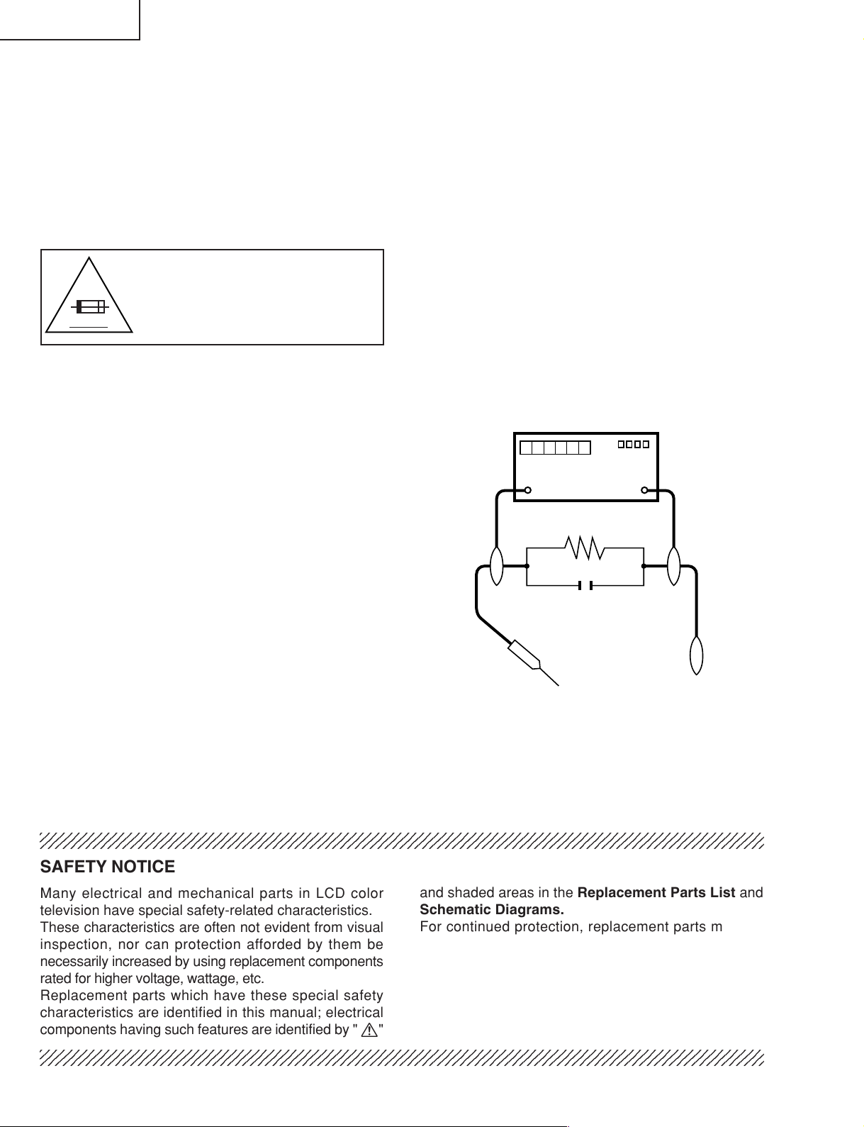
leakage current in the following manner.
» Plug the AC cord directly into a 110~240 volt AC outlet.
» Using two clip leads, connect a 1.5k ohm, 10 watt
resistor paralleled by a 0.15µF capacitor in series
with all exposed metal cabinet parts and a known
earth ground, such as electrical conduit or electrical
ground connected to an earth ground.
» Use an AC voltmeter having with 5000 ohm per volt,
or higher, sensitivity or measure the AC voltage drop
across the resistor.
» Connect the resistor connection to all exposed metal
parts having a return to the chassis (antenna, metal
cabinet, screw heads, knobs and control shafts,
escutcheon, etc.) and measure the AC voltage drop
across the resistor.
All checks must be repeated with the AC cord plug
connection reversed. (If necessary, a nonpolarized
adaptor plug must be used only for the purpose of
completing these checks.)
Any reading of 0.75 Vrms (this corresponds to 0.5
mA rms AC.) or more is excessive and indicates a
potential shock hazard which must be corrected
before returning the monitor to the owner.
DVM
AC SCALE
1.5k ohm
10W
0.15 µF
TEST PROBE
TO EXPOSED
METAL PARTS
CONNECT TO
KNOWN EARTH
GROUND
234567890123456789012345678901212345678901234567890123456789012123456789012345678901234567890121
SAFETY NOTICE
Many electrical and mechanical parts in LCD color
television have special safety-related characteristics.
These characteristics are often not evident from visual
inspection, nor can protection afforded by them be
necessarily increased by using replacement components
rated for higher voltage, wattage, etc.
Replacement parts which have these special safety
characteristics are identified in this manual; electrical
components having such features are identified by " å"
234567890123456789012345678901212345678901234567890123456789012123456789012345678901234567890121
and shaded areas in the Replacement Parts List and
Schematic Diagrams.
For continued protection, replacement parts must be
identical to those used in the original circuit.
The use of a substitute replacement parts which do not
have the same safety characteristics as the factory
recommended replacement parts shown in this service
manual, may create shock, fire or other hazards.
2
Page 3
TU-GA1U-S
2
2
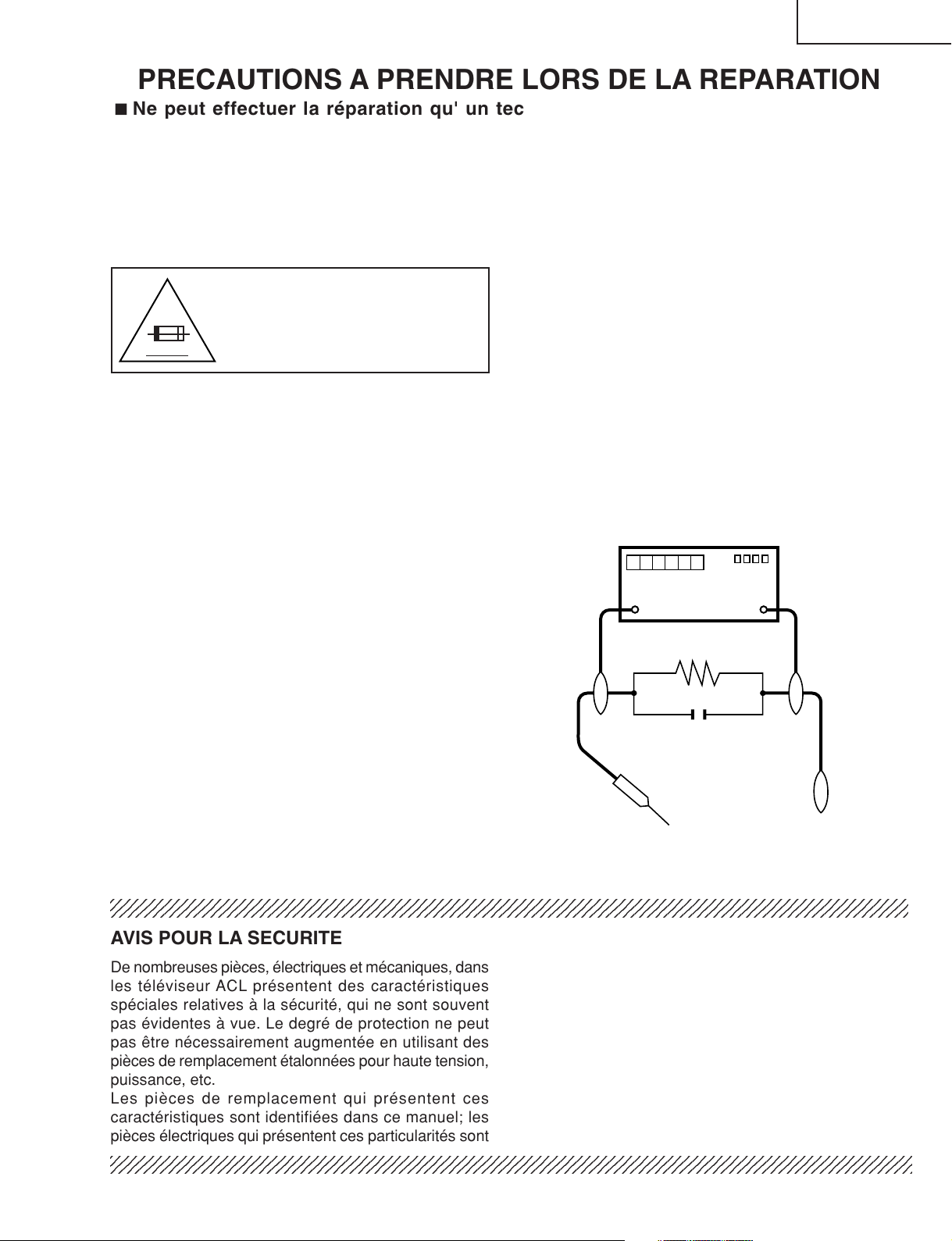
DVM
ECHELLE CA
1.5k ohm
10W
0.15 µF
SONDE D'ESSAI
AUX PIECES
METALLIQUES
EXPOSEES
BRANCHER A UNE
TERRE CONNUE
TU-GAD
PRECAUTIONS A PRENDRE LORS DE LA REPARATION
Ë
Ne peut effectuer la réparation qu' un technicien spécialisé qui s'est parfaitement
accoutumé à toute vérification de sécurité et aux conseils suivants.
AVERTISSEMENT
1. N'entreprendre aucune modification de tout circuit.
C'est dangereux.
2. Débrancher le récepteur avant toute réparation.
PRECAUTION: POUR LA
PROTECTION CONTINUE CONTRE
LES RISQUES D'INCENDIE,
A V
REMPLACER LE FUSIBLE
F701 (2A, 250V), F702 (1A, 250V)
VERIFICATIONS CONTRE L'INCEN-DIE ET
LE CHOC ELECTRIQUE
Avant de rendre le récepteur à l'utilisateur, effectuer
les vérifications suivantes.
1. Inspecter tous les faisceaux de câbles pour s'assurer
que les fils ne soient pas pincés ou qu'un outil ne soit
pas placé entre le châssis et les autres pièces
métalliques du récepteur.
2. Inspecter tous les dispositifs de protection comme les
boutons de commande non-métalliques, les isolants,
le dos du coffret, les couvercles ou blindages de réglage
et de compartiment, les réseaux de résistancecapacité, les isolateurs mécaniques, etc.
3. S'assurer qu'il n'y ait pas de danger d'électrocution en
vérifiant la fuite de courant, de la facon suivante:
• Brancher le cordon d'alimentation directem-ent à une
prise de courant de 110-240V. (Ne pas utiliser de
transformateur d'isolation pour cet essai).
• A l'aide de deux fils à pinces, brancher une résistance
de 1.5 kΩ 10 watts en parallèle avec un condensateur
de 0.15µF en série avec toutes les pièces métalliques
exposées du coffret et une terre connue comme une
conduite électrique ou une prise de terre branchée à
la terre.
• Utiliser un voltmètre CA d'une sensibilité d'au moins
5000Ω/V pour mesurer la chute de tension en travers
de la résistance.
• Toucher avec la sonde d'essai les pièces métalliques
exposées qui présentent une voie de retour au châssis
(antenne, coffret métallique, tête des vis, arbres de
commande et des boutons, écusson, etc.) et mesurer
la chute de tension CA en-travers de la résistance.
Toutes les vérifications doivent être refaites après avoir
inversé la fiche du cordon d'alimentation. (Si nécessaire,
une prise d'adpatation non polarisée peut être utilisée
dans le but de terminer ces vérifications.)
Tous les courants mesurés ne doivent pas dépasser
0.5 mA.
Dans le cas contraire, il y a une possibilité de choc
électrique qui doit être supprimée avant de rendre le
récepteur au client.
234567890123456789012345678901212345678901234567890123456789012123456789012345678901234567890121
AVIS POUR LA SECURITE
De nombreuses pièces, électriques et mécaniques, dans
les téléviseur ACL présentent des caractéristiques
spéciales relatives à la sécurité, qui ne sont souvent
pas évidentes à vue. Le degré de protection ne peut
pas être nécessairement augmentée en utilisant des
pièces de remplacement étalonnées pour haute tension,
puissance, etc.
Les pièces de remplacement qui présentent ces
caractéristiques sont identifiées dans ce manuel; les
pièces électriques qui présentent ces particularités sont
234567890123456789012345678901212345678901234567890123456789012123456789012345678901234567890121
identifiées par la marque " å " et hachurées dans la
liste des pièces de remplacement et les diagrammes
schématiques.
Pour assurer la protection, ces pièces doivent être
identiques à celles utilisées dans le circuit d'origine.
L'utilisation de pièces qui n'ont pas les mêmes
caractéristiques que les pièces recommandées par
l'usine, indiquées dans ce manuel, peut provoquer des
électrocutions, incendies, radiations X ou autres
accidents.
3
Page 4
TU-GA1U-S
TU-GAD
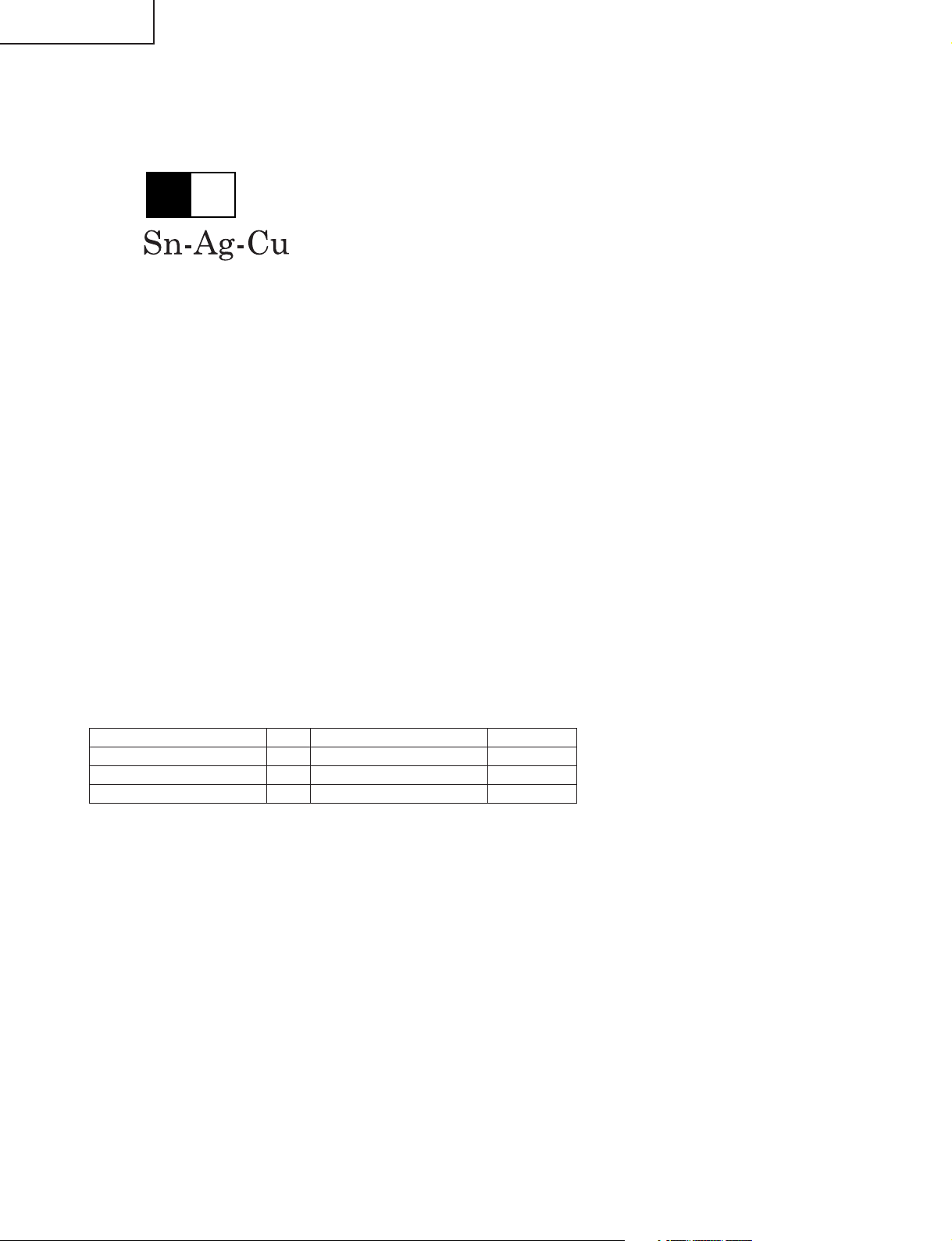
Precautions for using lead-free solder
1 Employing lead-free solder
"PWBs" of this model employs lead-free solder. The LF symbol indicates lead-free solder, and is attached on the
PWBs and service manuals. The alphabetical character following LF shows the type of lead-free solder.
Example:
L Fa
Indicates lead-free solder of tin, silver and copper.
2 Using lead-free wire solder
When fixing the PWB soldered with the lead-free solder, apply lead-free wire solder. Repairing with conventional
lead wire solder may cause damage or accident due to cracks.
As the melting point of lead-free solder (Sn-Ag-Cu) is higher than the lead wire solder by 40°C, we recommend
you to use a dedicated soldering bit, if you are not familiar with how to obtain lead-free wire solder or soldering bit,
contact our service station or service branch in your area.
3 Soldering
As the melting point of lead-free solder (Sn-Ag-Cu) is about 220°C which is higher than the conventional lead
solder by 40°C, and as it has poor solder wettability, you may be apt to keep the soldering bit in contact with the
PWB for extended period of time. However, Since the land may be peeled off or the maximum heat-resistance
temperature of parts may be exceeded, remove the bit from the PWB as soon as you confirm the steady soldering
condition.
Lead-free solder contains more tin, and the end of the soldering bit may be easily corroded. Make sure to turn on
and off the power of the bit as required.
If a different type of solder stays on the tip of the soldering bit, it is alloyed with lead-free solder. Clean the bit after
every use of it.
When the tip of the soldering bit is blackened during use, file it with steel wool or fine sandpaper.
Be careful when replacing parts with polarity indication on the PWB silk.
Lead-free wire solder for servicing
Part No, ★ Description Code
ZHNDAi123250E J φ0.3mm 250g(1roll) BL
ZHNDAi126500E J φ0.6mm 500g(1roll) BK
ZHNDAi12801KE J φ1.0mm 1kg(1roll) BM
4
Page 5
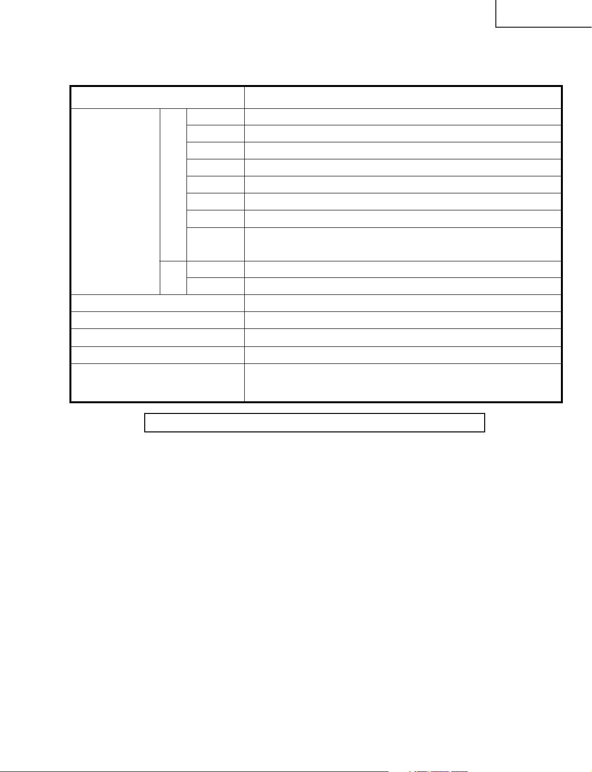
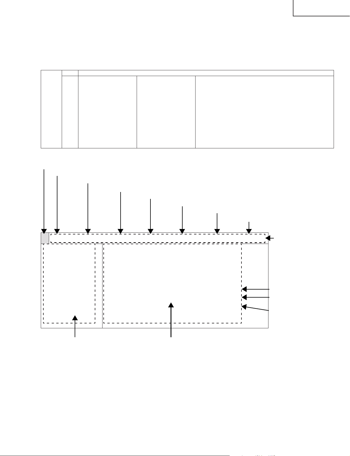
SPECIFICATIONS
Item
TU-GA1U-S /TU-GAD (AVC System)
Terminals
AV in, COMPONENT in
INPUT 2 AV in, COMPONENT in
INPUT 4
HDMI in
ANTENNA
75 Ω Unbalance, F Type for VHF/UHF/CATV in m 2, out m 1
INPUT 3 S-VIDEO in, AV in
OSD language English/French/Spanish
Power Requirement
AC 110-240 V, 50/60 Hz
48W (0.4W Standby with AC 120 V)
Weight
14.8 lbs./6.7 kg (w/o stand), 15.2 lbs./6.9 kg (with stand)
Accessories Operation manual ( 1), Remote
control unit ( ××1), System cable ( × 1),
AC cord ( × 2), "AAA" size battery
( ××2), AVC system stand unit ( × 1),
RF cable ( 1)
Rear INPUT 1
Front
Monitor Out S-VIDEO out, AV out
Headphones
Ø 3.5mm jack
CENTER
CHANNEL
INPUT
RCA pin
4 Ω 10W (L/R)SPEAKER-B
INPUT 5 Audio in, DVI-I in
Power Consumption
Specifications are subject to change without prior notice.
TU-GA1U-S
TU-GAD
5
Page 6
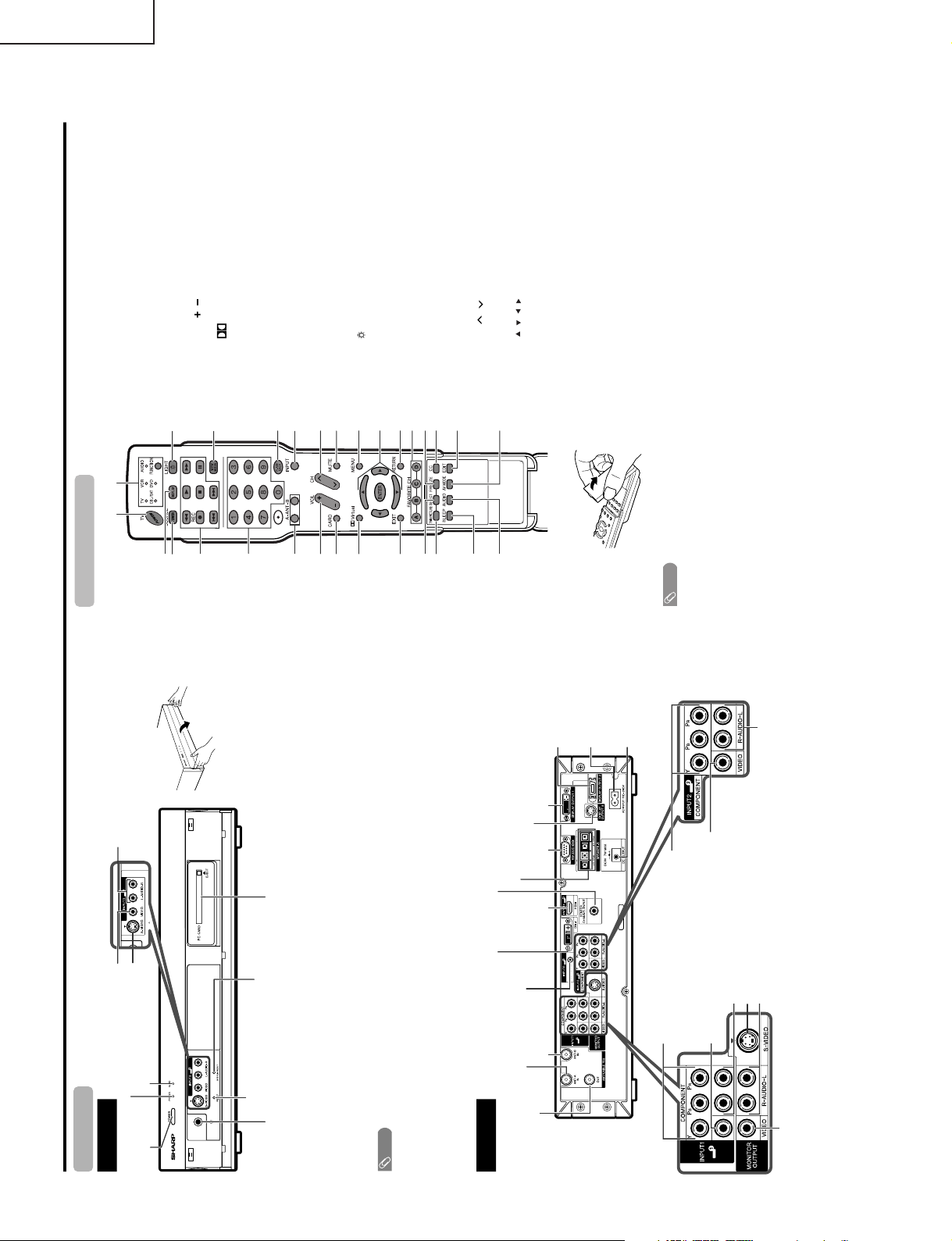
TU-GA1U-S
Part names
Front view
RESET*
POWER button
INPUT 3 terminal (S-VIDEO)
INPUT 3 terminal (VIDEO)
SYSTEM RESET**
INPUT 3 terminals (AUDIO L/R)
AVC System
Rear view
Antenna (A)
input terminal
Antenna (B)
input ter
minal
Antenna (A)
output terminal
How to open the door.
STANDBY/ON indicator
* Press RESET if the system cannot return to its original state after performing various operations.
• AV MODE resets to DYNAMIC (Fixed)
• TV channel returns to initial channel setting (Air:2ch, Cable:1 or 2ch)
• Twin picture resets to normal
• Audio setting initializes
• Dolby virtual resets to Off
• Image position initializes
** Press SYSTEM RESET if the system does not operate after starting up.
NOTE
• Pressing RESET will not work if the System is in standby mode (indicator lights red).
• Pressing RESET will not delete channel preset or secret number. See page 82 for clearing the secret number when you
know it. See page for initializing to the factory preset values when you forget your secret number.
Headphone
(When connecting headphones, the sound from the speakers is muted.)
DC OUTPUT
terminal
(Terminal for expanded
functionality in the near future.)
EXTERNAL SPEAKER terminals
PC CARD slot
CARD indicator
INPUT 1 COMPONENT
video terminals (Y, P
B
, P
R
)
INPUT 2 COMPONENT
video terminals (Y, P
B
, P
R
)
MONITOR OUTPUT terminal (S-VIDEO)
DISPLA
Y OUTPUT 1 terminal
DISPLAY
OUTPUT 2
terminal
AC INPUT
terminal
RS-232C
terminal
MONITOR OUTPUT terminals (AUDIO L/R)
INPUT 2 terminal (VIDEO)
INPUT 2 terminals (AUDIO L/R)
INPUT 1 terminal
(VIDEO)
INPUT 1 terminals (AUDIO L/R)
MONITOR OUTPUT terminal (VIDEO)
DISPLAY OUTPUT 3 terminal
Input 5 terminal
(AUDIO)
INPUT 5 terminal (DVI-I)
INPUT 4
terminal
(HDMI)
CENTER CHANNEL INPUT
Remote control unit
NOTE
• When using the remote control unit, point it at the Liquid
Crystal Television.
3
2
115
5
6
4
7
18
16
17
19
20
1
2
10 24
25
26
12
11
27
13
14 29
23
28
1 TV POWER: Switch the Liquid Crystal Television power
on or off.
2 DISPLAY: Display the channel information.
3 SOURCE POWER: Turns the power of the exter nal
equipment on and off.
4 External equipment operational buttons: Operate the
external equipment.
50 – 9: Set the channel.
6 ANT-A/B: Select between ANT-A and B to watch
broadcasts via the two tuners.
7VOL/ : Set the volume.
8 CARD: Switch to card mode.
9
Virtual: Select Virtual Dolby Surround settings.
10 EXIT: Turn off the menu screen.
11 SELECT: Select the active screen.
12 TWIN PICTURE: Set the twin picture mode.
Press again to return to normal screen.
13
SLEEP:
Set the sleep timer
.
14 AUDIO: Select the MTS/SAP.
15 FUNCTION: Switches the remote control for TV, VCR,
AUDIO, CBL/SAT and DVD operation. Indicator lights
up for the current mode.
16
: When pressed all buttons on the remote control unit
will light. The lighting will turn off if no operations are
performed within about 5 seconds. This button is used
for performing operations in dark places.
17 VIEW MODE: Select the screen size.
18 FLASHBACK: Return to the previous channel or input
external mode.
19 INPUT: Select a Liquid
Crystal Television input source.
(TV, INPUT 1, INPUT 2, INPUT 3, INPUT 4, INPUT 5,
Card)
20 CH / : Select the channel.
21 MUTE: Mute the sound.
22 MENU: Display the menu screen.
23 ///: Select a desired item on the screen.
24 RETURN: Return to the previous menu screen.
25 FAVORITE CH
A, B, C, D: Select four preset favorite channels in four
different categories.
While watching, you can toggle the selected channels
by pressing A, B, C and D.
26 FREEZE: Set the still image. Press again to return to
normal screen.
27 CC: Display captions during closed-caption source.
28
EDIT:
Register favorite channel.
29 AV MODE: Select an audio or video setting.
(AV mode: STANDARD, MOVIE, GAME,USER, DYNAMIC
(Fixed), DYNAMIC. PC mode:STANDARD, USER.)
TU-GAD
OPERATION MANUAL
6
Page 7
Using external equipment
AVC System
(rear view)
DVD player
Connecting a DVD player
You can use the INPUT 1, INPUT 2, INPUT 4 or INPUT 5 terminals when connecting to a DVD player and other
audiovisual equipment.
Audio cable (commercially available)
Component video cable
(commercially available)
When using component cable.
When using composite cable.
AV cable (commercially available)
DVD player
AVC System
(rear view)
ø 3.5mm stereo minijack cable
(commercially available)
When using DVI cable. (INPUT 5)
AVC System
(rear view)
DVI cable
(Commercially available)
DVD player
AVC System (rear view)
VCR
AV cable
(commercially available)
Connecting a VCR
You can use the INPUT 2 terminal when connecting a VCR and other audiovisual equipment.
AVC System (front view)
Game console/Camcorder
AV cable (commercially available)
S-video cable
(commercially available)
Connecting a game console or camcorder
A game console, camcorder and some other audiovisual equipment are conveniently connected using the
INPUT 3 terminals.
NOTE
• The S-video ter
minal has priority over the video terminals.
TU-GA1U-S
TU-GAD
7
Page 8
TU-GA1U-S
Using external equipment
AVC System (rear view)
Digital TV STB
Connecting a Digital TV STB
You can use the INPUT 1, INPUT 2, INPUT 4 or INPUT 5 terminals when connecting a Digital TV STB and other
audiovisual equipment.
Component video cable (commercially available)
Audio cable
(commercially available)
Digital TV STB
AV cable
(commercially available)
Digital
TV STB
ø 3.5mm stereo minijack cable
(commercially available)
When using component cable.
When using composite cable.
AVC System (rear view)
When using DVI cab
le. (INPUT 5)
AVC System (rear view)
DVI cable
(Commercially available)
Connecting HDMI equipment
You can use the INPUT 4 terminal when connecting an HDMI equipment.
HDMI equipment
HDMI cable
(Commercially available)
AVC System (rear view)
Displaying an image from HDMI equipment
To watch an HDMI equipment image, select
“INPUT4” from “INPUT SOURCE” menu
using INPUT on the remote control unit or
on the Display.
INPUT SOURCE
TV
INPUT1
INPUT2
INPUT3
INPUT4
INPUT5INPUT5
CARD
1
Press MENU and the MENU screen displays.
2
3
Press / to select “HDMI Setup”, and then
press ENTER.
4
Press / to select “Option”.
MENU
[
Option
...
HDMI Setup
]
Option
Digital Noise Reduction
Output Select
Center Channel Input
Caption Setup
Audio Only
Quick Shoot
[Fixed]
[Off]
HDMI Setup
[Auto]
[Low]
[Off]
5
Press / to select the desired item and
press ENTER.
Press / / / to select the desired setting
and press ENTER.
6
NOTE
• Refer to your external equipment operation manual for
the signal type.
Selectable items
Auto/RGB/YCbCr
4:4:4/YCbCr 4:2:2
Auto/ITU601/
ITU709
Standard/
Out of standard
Enable/Disable
HDMI Setup
items
Signal
Type
Color
Matrix
Dynamic
Range
Auto View
Description
Select the signal type from
an HDMI terminal. Unless
the image quality looks
obviously poor, select Auto.
Select the internal color
space conversion method
when an RGB signal is
input. Normally, select
Auto.
Select the signal amplitude
range. Normally, select
Standard.
Set whether or not to use
VIEW MODE based on
signal recognition,
including an HDMI signal.
TU-GAD
8
Page 9
Using external equipment
AVC System (rear view)
ø 3.5 mm stereo minijack cable
(commercially available)
PC with analog RGB terminal
Connecting a PC
Use the INPUT 5 terminal to connect a PC.
ø 3.5 mm stereo minijack cable
(commercially available)
DVI cable
(Commercially available)
RGB/DVI conversion cable
(Commercially available)
PC with DVI terminal
Rear view
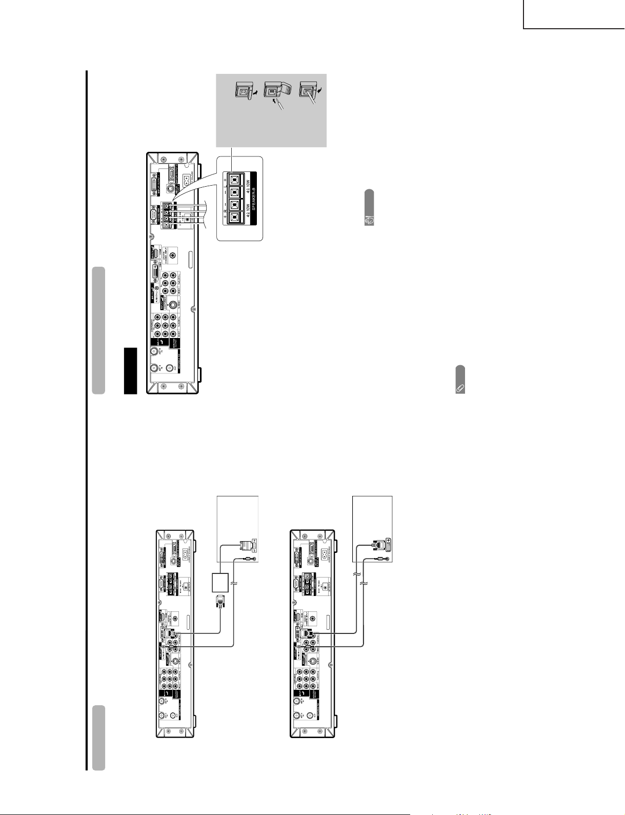
Connecting external speakers
When using external speakers
• Change the speaker setting to external speakers.
+
+
–
–
Make sure to connect the speaker terminal and
cable polarity ( , ) properly
• The speaker terminals have plus ( ) and minus ( )
polarity.
• Plus is red and minus is black.
• The cables are also divided into plus and minus.
• When connecting the left/right speakers, be sure to
connect the plus/minus terminals with the correct cables.
NOTE
• Unplug the AC cord from the AC outlet before installing
the speakers.
CAUTION
• Make sure external speakers have 4 ohm and 10 watt
specifications.
• Connect the plus/minus terminals with the correct cables.
Incorrect connection may cause a short.
How to connect the
speaker cable
Push down
the tab.
Insert the
end of the
cable.
Lift the tab
back up.
1
2
3
TU-GA1U-S
TU-GAD
9
Page 10
TU-GA1U-S
Appendix
PC compatibility chart
Apple and Macintosh are registered trademarks
of Apple Computer, Inc.
DDC is a registered trademark of Video Electronics
Standards Association.
Power Management is a registered trademark of
Sun Microsystems, Inc.
VGA and XGA are registered trademarks of
International Business Machines Co., Inc.
PC/MAC Resolution
Horizontal Frequency
Vertical Frequency
VESA Standard
PC
31.5 kHz
37.9 kHz
31.5 kHz
37.9 kHz
31.5 kHz
37.9 kHz
37.5 kHz
43.3 kHz
31.5 kHz
35.1 kHz
37.9 kHz
48.1 kHz
46.9 kHz
53.7 kHz
48.4 kHz
56.5 kHz
60.0 kHz
68.7 kHz
45.0 kHz
48.1 kHz
64.0 kHz
34.9 kHz
49.7 kHz
60.2 kHz
640 x 400
720 x 400
VGA
640 x 480
WVGA 848 x 480
SVGA
800 x 600
1024 x 768XGA
1280 x 720
WXGA
1280 x 768
SXGA
1280 x 1024
VGA
640 x 480
MAC13"
XGA
1024 x 768
MAC19"
SVGA
832 x 624
MAC16"
60 Hz
85 Hz
60 Hz
85 Hz
60 Hz
72 Hz
75 Hz
85 Hz
60 Hz
56 Hz
60 Hz
72 Hz
75 Hz
85 Hz
60 Hz
70 Hz
75 Hz
85 Hz
60 Hz
60 Hz
60 Hz
67 Hz
75 Hz
75 Hz
O
O
O
O
O
O
O
O
O
O
O
O
O
O
O
O
RS-232C port specifications
Return codeCommand 4-digits Parameter 4-digits
PC Control of the System
• When a program is set, the Display can be controlled from the PC using the RS-232C terminal.
The input signal (PC/AV) can be selected, the volume can be adjusted and various other adjustments and
settings can be made, enabling automatic programmed playing.
•
Attach an RS-232C cable cross-type (commercially available) to the supplied Din/D-Sub RS-232C for the
connections.
NOTE
• This operation system should be used by a person who is accustomed to using computers.
Communication conditions
Set the RS-232C communications settings on the PC to match the display
’
s communications conditions.
The Display’s communications settings are as follows:
Baud rate:
Parity bit:
Data length:
Stop bit:
Flow control:
9,600 bps
8 bits
None
1 bit
None
Command format
Communication procedure
Send the control commands from the PC via the RS-232C connector.
The display operates according to the received command and sends a response message to the PC.
Do not send multiple commands at the same time. Wait until the PC receives the OK response before sending
the next command.
Eight ASCII codes CR+
Command 4-digits:Command. The text of four characters.
Parameter 4-digits:Parameter 0 – 9, x, blank, ?
Parameter
Input the parameter values, aligning left, and fill with blank(s) for the remainder. (Be sure that 4 values are input for the
parameter.)
When the input parameter is not within an adjustable range,
“ERR” r
eturns. (Refer to “Response code format”.)
No problem to input any numerical value for
“x” on the table.
When “?” is input for some commands, the present setting value responds.
C1 C2 C3 C4 P1 P2 P3 P4
0055
100
30
0009
0
????
?
TU-GAD
10
Page 11
TU-GA1U-S
Command table
• About the command except being indicated here, it is outside the guarantee range of operation.
CONTROL ITEM COMMAND
PARAMETER
CONTROL CONTENTS
POWER SETTING It shifts to standby.
It input-switches by the toggle. (It is the same as an input change key)
It input-switches to TV. (A channel remains as it is. (Last memory))
It input-switches to INPUT1~INPUT5.
It shifts to CARD mode.
An input change is also included.
Although it can choose now, it is toggle operation in inside.
Although it can choose now, it is toggle operation in inside.
(Toggle)
Input terminal number (1
–5)
AUTO
VIDEO
COMPONENT
DIGITAL PC
ANALOG PC
DIGITAL AV
ANALOG AV
(Toggle)
STANDARD
MOVIE
USER
GAME
DYNAMIC (Fixed)
DYNAMIC
Volume (0–60)
AV mode. ( 10)
PC mode. (0–180)
AV mode. ( 20)
PC mode. (0–100)
Only PC mode. (0
–180)
Only PC mode. (0
–40)
(Toggle) [AV]
An input change is included if it is not TV display.
In Air, 2–69ch is effective.
In Cable, 1–125ch is effective.
If it is not TV display, it will input-switch to TV.
If it is not TV display, it will input-switch to TV.
Change toggle operation of tuner A/B.
Toggle operation of a closed caption.
(Toggle)
Side Bar [AV]
S.Stretch [AV]
Zoom [AV]
Stretch [AV]
Normal [PC]
Zoom [PC]
Stretch [PC]
Dot by Dot [PC]
On
Off
OFF
OFF TIMER – 30 MIN.
The channel number of TV
The channel number of TV 1
The channel number of TV 1
(Toggle)
(Toggle)
(1–125)
AUTO
POWR
ITGD
ITVD
IAVD
I CRD
INP1
INP5
INPUT SELECTION A TOGGLE
INPUT SELECTION B
AV MODE SELECTION
VOLUME
POSITION
VIEWMODE
Dolby Virtual
SLEEP TIMER
CHANNEL
ANT-A/B
CC
DIRECT
CH UP
CH DOWN
CHANNEL
H-POSITIONH-POSITION
V-POSITION
CLOCK
PHASE
INPUT 1
INPUT 5
AVMD
VOLM
HPOS
VPOS
CLCK
PHSE
ACDV
OFTM
DCCH
CHUP
CHDW
ANTS
CLCP
WIDE
0
x
0
*
x
0
5
6
7
8
1
2
0
*
*
*
*
*
0
0
*
x
x
x
x
1
1
2
0
1
2
3
4
5
6
7
8
*
*
1
2
3
4
5
6
*
_
_
_
_
_
_
_
_
_
_
_
_
_
_
_
_
_
_
*
*
*
*
*
*
*
_
_
_
_
_
_
_
_
_
_
_
_
_
_
_
_
_
_
_
*
_
_
_
_
_
_
_
_
_
_
_
_
_
_
_
_
_
_
*
*
*
*
*
*
_
_
_
_
_
_
_
_
_
_
_
_
_
_
_
_
_
_
_
_
_
_
_
_
_
_
(Toggle)
AUDIO SELECTION
ACHAx _ _ _
_
_
OFF TIMER – 60 MIN.
OFF TIMER – 90 MIN.
2
3
_
_
_
_
_
_
OFF TIMER – 120 MIN. 4___
_
_
(Toggle)
On
Off
MUTE
MUT E 0
1
2
_
_
_
_
_
_
_
_
_
_
_
_
_
_
_
_
_
_
_
_
_
_
_
_
_
_
_
_
_
_
_
_
_
_
_
_
_
AUTO
VIDEO
COMPONENT
AUTOINP2
INPUT 2
0
1
2
_
_
_
_
_
_
_
_
_
_
_
_
_
_
_
_
TV
INPUT1-5
CARD
Appendix
NOTE
• If an underbar (_) appears in the parameter column, enter a space.
• If an asterisk (*) appears, enter a value in the range indicated in brackets under CONTROL CONTENTS.
• As long as that from which the parameter ( × ) in the table is a numerical value, it may write anything.
Return code (0DH)
Response code format
Normal response
Problem response (communication error or incorrect command)
Return code (0DH)
OK
ERR
Basic adjustment settings
AV input mode menu items
List of AV menu items to help you with
operations
OPC
Brightness
Contrast
Black Level
Color
Tint
Sharpness
Advanced
C.M.S.
Color Temp.
Black
3D-Y/C
Monochrome
Film Mode
I/P Setting
Picture
No Signal Off
No Operation Off
EZ Setup
CH Setup
Speaker Setup
Input Label
Parental CTRL
Position
Picture Flip
Langua
ge
Treble
Bass
Balance
Dolb
y Virtual
Audio Only
Digital Noise Reduction
HDMI Setup
Input Select
Output Select
Quick Shoot
Center Channel Input
Caption Setup
Audio
Power Control
Setup
Option
PC input mode menu items
List of PC menu items to help you with
operations
OPC
Backlight
Contrast
Brightness
Red
Green
Blue
Advanced
C.M.S.
Picture
Power Management
Speaker Setup
Input Signal
Auto Sync.
Input Label
Fine Sync.
Picture Flip
Language
Audio
Power Control
Setup
Treble
Bass
Balance
Dolby Virtual
Option
Audio Only
Input Select
Output Select
Quic
k Shoot
Center Channel Input
TU-GAD
11
Page 12
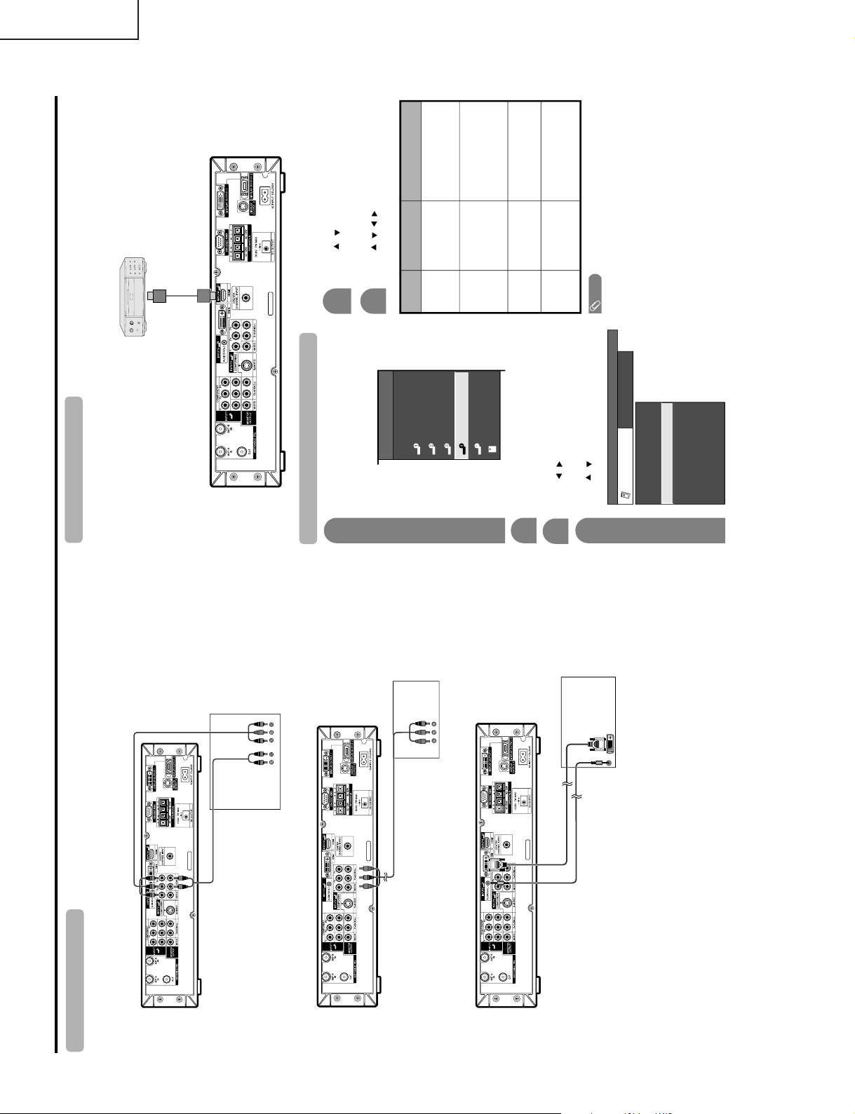
TU-GA1U-S
TU-GAD
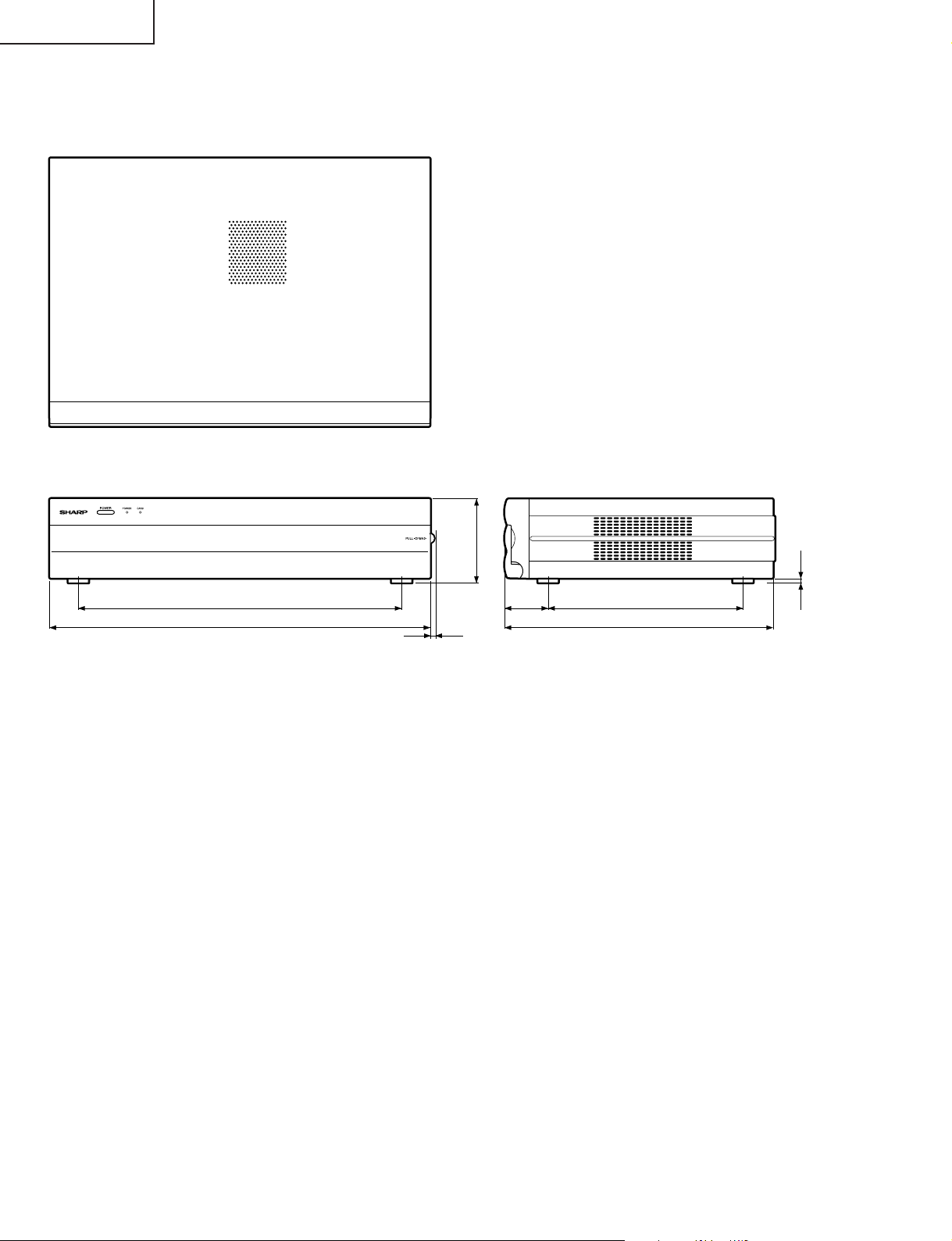
DIMENSIONS
Unit: inch/(mm)
1423/64(365)
1659/64(430)
5
/64(2)
47
(95)
64
/
3
821/32(220)159/64(49)
1159/64(303)
(5)
16
/
3
12
Page 13
TU-GA1U-S
TU-GAD
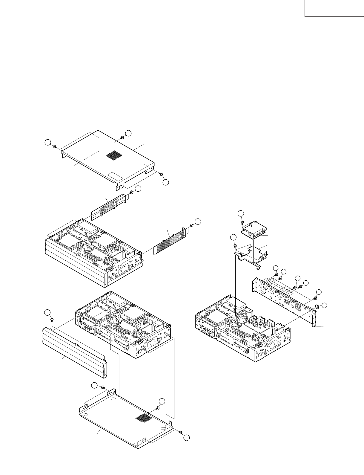
REMOVING OF MAJOR PARTS
1. Remove the two lock screws from each of the right and left side covers, and detach the side covers by sliding
them backward.
2. Remove the five lock screws from the top cabinet, and detach the cabinet by sliding it backward.
3. Remove the lock screws from the bottom cabinet, and detach the cabinet by sliding it backward.
4. Remove the tow lock screws from the front panel, and detach the panel.
5. Remove the lock screws, four tuner nuts and six hexagon shaft screws from the rear chassis, and detach the rear
chassis.
6. Remove the DVI PWB.
6-1. Remove the four lock screws from the DVI PWB angle.
6-2. Remove the four lock screws from the DVI PWB.
2
2
2
Top Cabinet
2
1
Side Cover (left)
6-2
Side Cover (right)
4
1
6-1
DVI PWB
DVI PWB Angle
5
5
5
5
5
5
Rear Chassis
Front Panel
3
Bottom Cabinet
3
3
13
Page 14
TU-GA1U-S
TU-GAD
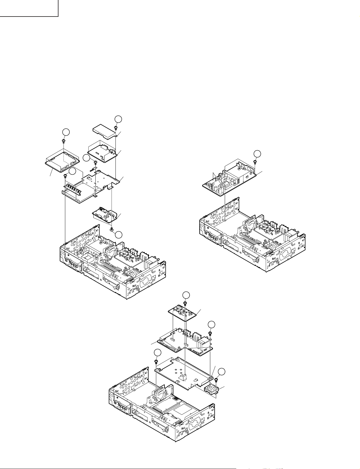
7. Remove the DC/DC converter PWB, TMDS PWB and AUDIO I/F PWB.
7-1. Remove the three lock screws from the TMDS PWB angle.
7-1. Remove the four lock screws from the DC/DC converter PWB.
7-3. Remove the four lock screws from the TMDS PWB.
7-4. Remove the two lock screws from the AUDIO I/F PWB.
8. Remove the five lock screws from the power PWB.
9. Remove the AV PWB, AV SUB PWB and 1-bit amplifier PWB.
9-1. Remove the four lock screws from the AV PWB angle.
9-2. Remove the one lock screw from the AV SUB PWB.
9-3. Remove the two lock screws from the 1-bit AMP PWB.
7-3
DC/DC Converter PWB
7-2
7-1
7-1
TMDS PWB Shield
TMDS PWB
TMDS PWB Angle
AUDIO I/F PWB
7-4
8
Power PWB
9-2
AV PWB
AV SUB PWB
9-1
9-1
AV PWB Angle
9-3
1-bit Amp PWB
14
Page 15
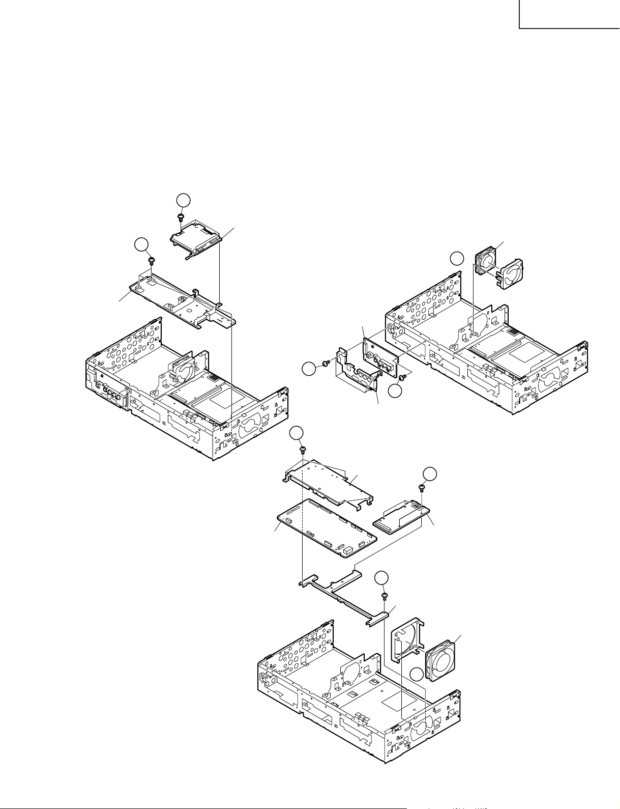
10. Remove the PC card PWB.
10-1. Remove the three lock screws from the PC card PWB angle.
10-2. Remove the four lock screws from the PC card PWB.
11. Remove the cooling fan (small) and front terminal PWB.
11-1. Detach the cooling fan (small).
11-2. Remove the four lock screws from the front shield.
11-3. Remove the one lock screw from the front terminal PWB.
12. Remove the cooling fan (large), main PWB and CPU PWB.
12-1. Detach the cooling fan (large).
12-2. Remove the four lock screws from the main PWB.
12-3. Remove the two lock screws from the CPU PWB.
12-4. Remove the lock screw from the main PWB angle.
10-2
TU-GA1U-S
TU-GAD
10-1
PC CARD PWB Angle
PC CARD PWB
12-2
11-2
Front PWB
Front Shield
MAIN PWB Shield
Cooling Fan (small)
11-1
11-3
12-3
MAIN PWB
CPU PWB
12-4
MAIN PWB Angle
Cooling Fan (large)
12-1
15
Page 16

TU-GA1U-S
TU-GAD
ADJUSTMENT PROCEDURE
This section describes the adjustment procedures which should be followed after replacement of faulty PWB (unit),
with special emphasis on the precautions to be taken after replacement of Main Unit (DUNTKC619) or CPU Unit
(DUNTKC427).
[Replacement of faulty CPU Unit]
1. Adjustment data are stored in the Main Unit. Therefore, no adjustment is needed after replacement of the CPU Unit.
[Replacement of faulty Main Unit]
1. A new Main Unit has no adjustment data. Therefore, all items need to be adjusted.
[Replacement of faulty IC2102 inside Main Unit]
1. A new IC2102 has no adjustment data. However, the data stored in the CPU Unit are automatically recognized and
loaded. Therefore, no adjustment is necessary.
Important * Be sure to follow the step below.
[Precaution after PWB replacement or adjustment]
1. After replacement of PWB or adjustment of each part, set "KEY WRITE" to "ON" which is shown in the
adjustment OSD menu (Page 2/15). Then press "Enter" and reboot the system.
16
Page 17

TU-GA1U-S
TU-GAD
[Precaution after adjustment] * Be sure to follow the step below.
1. After adjustment of each part, select "KEY WRITE" in the adjustment OSD menu (Page 2/15) and set it to "ON"
using the "VOL (+)/(–)" key. Then press "Enter" and reboot the system.
[Entering the process adjustment mode]
Caution: Use due care in handling the information described here lest your users should know how to
enter the process adjustment mode. If the settings are tampered in this mode, unrecoverable
system damage may result.
1) Connect the Display and the AVC system using the system cable. Plug the power cable of each unit into
a wall outlet.
Power up the system using the power switch of the remote controller or the main unit.
2) Enter the standby mode using the remote controller or the main unit switch. (Both the power LED of the
Display and that of the AVC system light up in red.)
3) Press "Power" switch of the Display and shut off the power.
4) While simultaneously pressing the "VOL (–)" key and "INPUT" key of the Display, press "Power" switch of
the Display and turn on the power.
(Keep pressing the "VOL (–)" and "INPUT" keys until the specific display appears on the screen.)
If you have failed (only the ordinary startup display appeared), try this step again.
5) Make sure that a K mark is displayed in the top left of the screen.
6) Simultaneously press the "VOL (–)" key and the "CH(Ù)" key of the Display.
Several blue text lines appearing on the screen indicate the successful entry into the process adjustment
mode.
[Exiting the process adjustment mode]
1) You can exit the process adjustment mode by pressing "Power" switch of the Display and shutting off the
power.
[Remote controller key operation]
Channel up/down keys: Moves selection line by line (up/down).
Volume up/down keys: Changes setting of the selected line (+1/-1).
Cursor up/down keys: Navigates the page (previous/next).
Cursor right/left keys: Changes setting of the selected line (+10/-10).
Input: Cycles the input.
(TUNER → BSD → INPUT1 → INPUT2 → INPUT 3 → INPUT4 → INPUT5)
Enter: Executes the functions.
* With the necessary input signals being fed, the input switches itself after the relevant adjustment gets
started. Supply the video and component signals to INPUT1.
[Others]
* Viewing factory settings (backup data)Select EEP RECOVER in the adjustment OSD menu (Page 12/12).
Using "VOL (+)/(–)" key, change the setting from "OFF" to "ON". Then press "ENTER" key.
17
Page 18
TU-GA1U-S
TU-GAD
[Adjustment procedure]
* Before entering the process adjustment mode, press "TV Reset" switch on the AVC system. Or enter the TV
menu video adjustment mode, change the AVC position to "Dynamic" and execute "Reset" in the bottom of the
menu.
1) N358 signal adjustment [N358ALLADJ]
Adjusting point Adjusting conditions Adjusting procedure
1 Input signal setting
1) Input signal setting
1) Using the input signal generator, feed the split field
color bar signal -- US10ch (193.25 MHz), RF
modulation -- to the tuner -A/-B.
• Color saturation 75%
Yellow
White 75%
Cyan
White
100%
Green
Red
Magenta
• RF modulation 87.5%
Black
• Bottom white window Vertical: 1/4V
2 RF input/Video input
MAIN/SUB screen
• Contrast
• CB / CR GAIN
2) Video 1 input terminal
connection signal
Red
White
Yellow
Cyan
Green
Magenta
Blue
Feed the signal adjusted as
above.
2) Using the input signal generator, feed the full field
color bar signal to the Video 1 input terminal.
• Color saturation 75%
• Input signal should be 1.00 Vp-p (Sync - 100%
white) with 75Ω termination of the signal
Black
generator video output.
1) Enter the process adjustment mode.
2) Bring the cursor on to [N358 ALL ADJ] on Page 3.
3) Press [ENTER] key of the remote controller. The
adjustment is done automatically.
Ë For each input, operate in the following order.
1) Video input: Bring the cursor on to [N358 MAIN
ADJ] and press [ENTER].
2) Video input: Bring the cursor on to [N358 SUB ADJ]
on Page 4 and press [ENTER].
3) RF input: Bring the cursor on to [TUNER DAC ADJ]
and press [ENTER].
18
Page 19
2) 15K component signal adjustment [COMP15KALLADJ]
Adjusting point Adjusting conditions Adjusting procedure
1 Input signal setting
Video 1 component input
terminal connection signal
Red
White
Yellow
Cyan
Green
Magenta
Blue
1) Using the input signal generator, feed the full field
color bar signal to the Video 1 input terminal.
• Color saturation 100%
• Input signal should be 1.00 Vp-p (Sync - 100%
white) with 75Ω termination of the signal
Black
generator video output.
TU-GA1U-S
TU-GAD
2 15K component signal
input
Feed the signal adjusted as
above.
• Contrast
• CB / CR GAIN
• Y / CB / CR OFFSET
3) HDTV component signal adjustment [HDTV ADJ]
Adjusting point Adjusting conditions Adjusting procedure
1 Input signal setting
Video 1 component input
terminal connection signal
Cyan
White
Yellow
Green
Magenta
Red
1) Enter the process adjustment mode.
2) Bring the cursor on to [COMP15K ALL ADJ] on
Page 5.
3) Press [ENTER] key of the remote controller. The
adjustment is done automatically.
1) Using the input signal generator, feed the full field
color bar signal to the Video 1 component input
terminal.
• Color saturation 100%
• Input signal should be 1.00 Vp-p (Sync - 100%
Blue
Black
white) with 75Ω termination of the signal
generator video output.
2 HDTV component
signal input
• CONTRAST
• CB GAIN
• CR GAIN
• Y OFFSET
• PB OFFSET
• PR OFFSET
Feed the signal adjusted as
above.
19
1) Enter the process adjustment mode.
2) Bring the cursor on to [HDTV ADJ] on Page 7.
3) Press [ENTER] key of the remote controller. The
adjustment is done automatically.
Page 20
TU-GA1U-S
TU-GAD
4) DVI signal adjustment [DVI ANALOG / DVI DIGITAL]
Adjusting point Adjusting conditions Adjusting procedure
1 Input signal setting
DVI input terminal
connection signal
(Digital/analog)
100%
white
1) Using the input signal generator, feed the window
pattern signal to the DVI input terminal (digital/
analog).
• White 100%, black 0%
• Input signal should be 0.7 Vp-p (DATA 255) with
75Ω termination of the signal generator video
output.
0%
2 DVI input signal
Feed the signal adjusted as
above.
1) Enter the process adjustment mode.
2) Bring the cursor on to [DVI ANALOG] on Page 8.
3) Press [ENTER] key of the remote controller. The
adjustment is done automatically.
4) Bring the cursor on to [DVI DIGITAL] on Page 9.
5) Press [ENTER] key of the remote controller. The
adjustment is done automatically.
5) Finishing the adjustment
• Exit the process adjustment mode. (Press "Power" switch of the Display and shut off the power.)
Reference: To adjust each item manually, refer to the remarks in the process adjustment mode list for the detail.
Bring the cursor on to the desired item, and make adjustment using the Volume key.
(Adjustments will be less precise.)
[Retrieval of factory settings]
Caution: Once the factory setting retrieval is performed, all user data including channel settings will be lost by initialization.
Take enough care when performing this function. (The adjustments made in the process adjustment mode
will remain intact.)
Adjusting point Adjusting conditions Adjusting procedure
1 Factory settings
1) Enter the process adjustment mode.
2) Bring the cursor on to [INDUSTRY INIT] on Page 2.
3) Using [VOL] key, set to [ON]. Press [ENTER] to
execute initialization.
When the initialization is over, the system exits the
process mode automatically and displays TV 1ch.
4) * Never shut off the power until the initialization is
complete.
20
Page 21
Process adjustment mode list
•
Page Line Item Description Remarks (adjustment detail, etc.)
1 [INFO]
1 MAIN Version
2 CARD Version Card unit version Card unit
3 Monitor Version Monitor version Taken from the monitor. (Panel size and type also displayed)
4 EQ DATA CHECKSUM
5 STANDBY CAUSE Standby cause Last status which caused standby
6 FAN STATUS ROTATE
2 [INIT]
1 INDUSTRY INIT Factory settings Factory settings (common to factory settings of remote controller)
KEY WRITE Setting after PWB replacement and adjustment
HOTELMODE Prohibited
Center Acutime Total AVC operating hours
RESET
BacklightAcutime
RESET
VIC XPOS X-axis setting
VIC YPOS Y-axis setting
VIC COLOR Y/G, CB/B and CR/R settings
VIC SIGNAL_TYPE Singal setting adjustment
VIC READ Tum ON and press [ENETR], to get the setting displayed
3 [N358MAIN]
1 N358 ALL ADJ N358MAIN+SUB+TUNER Auto N358 Main, Sub and Tuner DAC adjustments
N358 MAIN ADJ Auto MAIN ADJ Auto N358 Main video adjustment
TUNER DAC ADJ Auto TUNER DAC Auto Tuner DAC adjustment
N358 MAIN CONTRAST IC400 Contrast adjustment
N358 MAIN Cb GAIN IC400 Cb gain adjustment
N358 MAIN Cr GAIN IC400 Cr gain adjustment
N358 SUB CONTRAST IC500 Sub contrast adjustment
N358 SUB Cb GAIN IC500 Sub Cb gain adjustment
N358 SUB Cr GAIN IC500 Sub Cr gain adjustment
TUNER A DAC TUNER-A DAC Tuner-A DAC adjustment
TUNER B DAC TUNER-B DAC Tuner-B DAC adjustment
4 1 N358 SUB ADJ Auto SUB ADJ Auto N358 Sub video adjustment
N358 SUB CONTRAST
N358 SUB Cb GAIN
N358 SUB Cr GAIN
TUNER TEST
TUNER VCHIP TEST(10ch) VCHIP TEST(10ch)
TUNER VCHIP TEST(15ch) VCHIP TEST(15ch)
5 [COMP15KMAIN]
1 COMP15K ALL ADJ Auto ALL Auto COMP15K Main + Sub adjustments
COMP15KAD MAIN ADJ Prohibited
COMP15K MAIN ADJ Auto ALL Auto COMP15K Main video adjustment
COMP15K MAIN CONTRAST
COMP15K MAIN Cb GAIN IC3700 Comp Cb gain adjustment
COMP15K MAIN Cr GAIN IC3700 Comp Cr gain adjustment
COMP15K Y OFFSET IC3700 Comp Y offset adjustment
COMP15K Cb OFFSET IC3700 Comp Cb offset adjustment
COMP15K Cr OFFSET IC3700 Comp Cr offset adjustment
COMP15K SUB CONTRAST
COMP15K SUB Cb GAIN IC500 Comp sub Cb gain adjustment
COMP15K SUB Cr GAIN IC500 Comp sub Cr gain adjustment
6 [COMP15KSUB]
1 COMP15K SUB ADJ Auto ALL Auto COMP15K Sub video adjustment
COMP15K SUB CONTRAST
COMP15K SUB Cb GAIN
COMP15K SUB Cr GAIN
7 [HDTV]
1 HDTV ADJ Auto HDTV video adjustment
CONTRAST IC3700 Contrast adjustment
Cb GAIN IC3700 Cb gain adjustment
Cr GAIN IC3700 Cr gain adjustment
HDTV Y OFFSET IC3700 HD Comp Y offset adjustment
HDTV Cb OFFSET IC3700 HD Comp Cb offset adjustment
HDTV Cr OFFSET IC3700 HD Comp Cr offset adjustment
Main microprocessor version
EQ DATA checing
Total monitor operating hours
IC3700 Comp contrast adjustment
IC500 Comp sub contrast adjustment
Version display
microprocessor
Check the EQ DATA
software version
TU-GA1U-S
TU-GAD
21
Page 22
TU-GA1U-S
TU-GAD
8 [DVI ANALOG]
1 DVI ANALOG Auto DVI analog video adjustment (W/B adjustment)
9 [DVI DIGITAL]
1 DVI DIGITAL Auto DVI digital video adjustment
10 [M GAMMA]
1 MONITOR R GAMMA LO Monitor W/B adjustment
11 [M GAMMA R]
1 MONITOR R GAMMA 1
12 [M GAMMA G]
1 MONITOR G GAMMA 1
13 [M GAMMA B]
1 MONITOR B GAMMA 1
14 [PATTERN]
1 CVIC PATTERN Prohibited
15 [ETC]
R CUTOFF IC3700 R cutoff adjustment
G CUTOFF IC3700 G cutoff adjustment
B CUTOFF IC3700 B cutoff adjustment
R DRIVE IC3700 R drive adjustment
G DRIVE IC3700 G drive adjustment
B DRIVE IC3700 B drive adjustment
CONTRAST IC3700 Contrast adjustment
R CUTOFF IC3700 R cutoff adjustment
G CUTOFF IC3700 G cutoff adjustment
B CUTOFF IC3700 B cutoff adjustment
R DRIVE IC3700 R drive adjustment
G DRIVE IC3700 R drive adjustment
B DRIVE IC3700 R drive adjustment
MONITOR G GAMMA LO
MONITOR B GAMMA LO
MONITOR R GAMMA HI
MONITOR G GAMMA HI
MONITOR B GAMMA HI
GAMMA WRITE
GAMMA RESET
MONITOR R GAMMA 2
MONITOR R GAMMA 3
MONITOR R GAMMA 4
MONITOR R GAMMA 5
MONITOR GAMMA 6
GAMMA WRITE
GAMMA RESET
MONITOR G GAMMA 2
MONITOR G GAMMA 3
MONITOR G GAMMA 4
MONITOR G GAMMA 5
MONITOR B GAMMA 6
GAMMA WRITE
GAMMA RESET
MONITOR B GAMMA 2
MONITOR B GAMMA 3
MONITOR B GAMMA 4
MONITOR B GAMMA 5
MONITOR B GAMMA 6
GAMMA WRITE
GAMMA RESET
PU PATTERN Prohibited
EEP SAVE Prohibited
EEP RECOVER Recovery of process Retrieves the stored adjustment value
adjustment value
CARD REC INPUT Prohibited
22
Page 23
TU-GA1U-S
TU-GAD
Ë
Manual adjustment
» First select Adjustment Items A and B. The adjustment points will be displayed at the top left.
» Then select Adjustment Items C and D. Set VIC READ to [ON] and press ENTER, and the adjustment data will
be displayed at top right.
» Finally switch to the adjustment page. Using the VOL (+)/(—) keys, go to the data and change the setting.
2 [INIT]
1 INDUSTRY INIT Factory setting
A VIC XPOS X-axis setting
B VIC YPOS Y-axis setting
C VIC COLOR Y/G, CB/B and CR/R settings
D VIC SIGNAL_TYPE Adjustment signal setting
Adjustment point
(1) Current page
(2) Current title
KEY WRITE Settings made after replacement and adjustment of PWB
HOTELMODE Prohibited
Center Acutime AVC total operating hours
RESET
BacklightAcutime
RESET
VIC READ Turn ON and press ENTER to get the setting displayed.
Monitor total operating hours
(3) Current input
(4) Current color system
(5) AVC HDCP key status (separate only)
Factory setting (remote controller factory setting and common operation)
(6) AVC destination
(7) Adjustment value (yellow)
2/15 [INIT] INPUT1 N358 HDCP:ON JAPAN VIC[ 240]
INDUSTRY INIT
KEY WRITE
HOTELMODE
Canter Acutime
RESET
Backlight
RESET
VIC XPOS
VIC YPOS
VIC COLOR
VIC SIGNAL_TYPE
VIC READ
OFF
OFF
OFF
`H`M
OFF
`H`M
OFF
0
0
Y/G
N358MAIN
OFF
(8) Item name (9) Parameter display
Process menu header
Adjustment signal selected
Adjustment input signal
selected
Adjustment value GO
23
Page 24
TU-GA1U-S
TU-GAD
B/W
[IRE]
CVBS Y 0/100 CONTRAST 234
CB/CR 75% Cb/Cr GAIN 198 Adjust with CB. Same value to CR.
2 RF 0/100 CONTRAST 234
3 NT-Comp Y 0/100 CONTRAST 245
PB/PR 100% Cb/Cr GAIN 240 Adjust with CB. Same value to CR.
4 HD-Comp Y 0/100 CONTRAST 245
PB/PR 100% PB/PR GAIN 240
PB/PR/ offset 0 PB/PR offset 0 Lower the setting to achieve 0.
5 DVI-A R/G/B 100 WB adjustment 240
RGB offset 0 0 Lower the setting to achieve 0.
6 DVI-D R/G/B 100 WB adjustment 240
RGB offset 0 0 Lower the setting to achieve 0.
PC Card Unit Y No adjustment
PB/PR
ADJ
Adjustment
reference data
(Note that the setting below "0" is not displayed.)
(Note that the setting below "0" is not displayed.)
(Note that the setting below "0" is not displayed.)
Digital Unit Y No adjustment
PB/PR
24
Page 25
TROUBLE SHOOTING TABLE
No power supply (Front LED is not ON)
TU-GA1U-S
TU-GAD
Is power cable properly connected to the main unit?
YES
Is F701 normal?
YES
Is F702 normal?
YES
Is BU+5V line (pin (5) of P1701) normal?
YES
Reconnect the wire harness, FFC, etc. in the set, and repeat
the check.
No power-up (Front LED does not change from red to green)
Are MDR (gray) and DVI (white) connectors of the system
cable properly connected to the Dispay and the AVC System?
NO
NO
NO
NO
NO
Connect the power cable properly, and turn on the power.
Replace F701, and turn on the power. If the fuse is still
blown, replace VA701, D701, Q705 and Q706, and repeat
Replace F702, and turn on the power. If the fuse is still
blown, replace D701 and IC701, and repeat the check.
Is there any faulty part or short-circuit in BU+5V line?
YES
Check IC902 and its peripheral
Remove the faulty part or short-circuit, and repeat the check.
Reconnect properly and turn on the power.
NO
YES
Is the power switch of the monitor ON?
YES
Is specified voltage available at S-Vcc+15V (pins (11) and
(12) of P1752), UR+10V (pin (5) of P1752) and CPU+10V
(pins (7) and (8) of P1781)?
YES
Is specified voltage available at D+1.8VCV (pins (3) and (4)
of P1703), D+3.3V (pins (9) and (12) of P1701) and D+5V
(pin (1) of P1703)?
YES
Is D_POW line normal? Are the pins
(46), (47) and (48) of IC1701 at "HI",
and the pin (5) of IC952 at "LOW"?
Check D_POW line.
Does OVP line voltage
fluctuate immediately after
the power is supplied?
NO
Reconnect the wire harness, FFC,
etc. in the set, and repeat the check.
NO
NO
NO
NO
YES
Set the power switch to ON, and turn on the power.
Are PS_ON (pin (6) of P1701) and EU_D_POWER (pin (2) of
P1702) at "HI" (3V or higher)?
YES
Check PS_ON or EU_D_POWER
Is specified impedance available in S-Vcc+15V, UR+10V and
CPU+10V lines? (Measure the resistance between each +B
line and GND.)
YES
Check the circuits in the faulty line.
Are MOS-FET (Q1701, Q1702, Q1703, Q1704 and Q1705)
and IC952 normal?
YES
Replace IC1701.
Replace faulty FET or IC.
NO
NO
NO
25
Page 26
TU-GA1U-S
TU-GAD
TROUBLE SHOOTING TABLE (Continued)
No audio output (1)
No headphone audio output
Check between pins (26) and (27) (OUT
L/R) of IC2702 and HPAMP (IC2502), audio
mute (Q2501) and headphone terminal
(J2402), as well as their peripheral circuits.
NO
Check the headphone plug check circuit.
Check between headphone (pin (4) of
J2402) and pin (7) of IC1102.
No audio output during BS reception
No monitor audio output
Check if monitor audio output is set to
"variable" or if headphone is connected.
NO NO
Is there normal audio output in IC2501
(Multi Sound Processor)?
Check pins (37) and (38) (SC10 OUT L/R)
of IC2501.
NO
Check between pins (37) & (38) (SC10
OUT L/R) of IC2501 (Multi Sound
Processor) and pins (1) & (13) of monitor
switching IC1108.
Is there normal audio output for each?
NO
Check between pins (1) & (13) of IC1108
and pins (2) & (5) of monitor audio output
terminal (J1105).
No audio output (2)
No BS monitor audio output
Is there normal audio output from the
main unit? Check pins (9) and (7) (L/R
OUT) of the connector (P1105).
Check between pins (9) & (7) (L/R OUT)
of P1105 and pins (1) & (13) of monitor
switching IC1108. Is there normal audio
output for each?
NO
Check between pins (1) & (13) of IC1108
and pins (2) & (5) (Q1102, Q1103) of
monitor audio output terminal (J1105).
No audio output during UHF/VHF
reception
Is the volume icon set on speaker
when volume key is operated?
YES
Are there normal signal inputs at pin
(2) of IC3805 and pin (2) of IC3812
(AV SW)?
YES
Are there normal signal inputs at pin
(3) of IC3805 and pin (3) of IC3812
(AV SW) to pins (56) and (57) of
IC2501 (Multi Sound Processor)?
YES
Are there normal audio outputs at pins
(33) and (34) (SC2 OUT L/R) of
IC2501 (Multi Sound Processor) to
pins (32) and (33) of IC2702?
YES
Are there normal audio outputs at pins
(28) and (29) (AOUT L/R) of IC2702?
YES
Are there normal audio outputs at pins
(28) and (29) of IC2702 to pins (13) and
(15) of P3801 (1-bit amplifier input)?
YES
Is relay switching done normally from
AUDIO I/F PWB P6003 to RY6001
(speaker switching) and RY6000
(speaker A/B switching)?
NO
NO
NO
NO
NO
NO
NO
If monitor output is set to "variable" in the
main menu, change the setting to "fixed".
Check between pins (9) & (7) (L/R
OUT) of P1105 and pins (59) & (61)
of IC3800 (AV SW).
Are there normal inputs and outputs
of I2S/LRCK, BICK, SDTO and SDTI
signals between IC2702 and IC2700
(DSP)?
Check between pins (33) & (34)
(SC2 OUT L/R) of IC2501 (Multi
Sound Processor) and pins (32) &
(33) of IC2702.
Check IC2702 and its peripheral
circuits.
Check the circuits between pins (28) &
(29) of IC2702 and pins (13) & (15) of
P3801 (1-bit amplifier input.)
Check the 1-bit amplifier and its
peripheral circuits.
NO
Is the volume icon set on speaker
when volume key is operated?
Is there normal signal input at pin (67)
(SOUND IF1) of IC2501 (Multi Sound
Processor)?
NO
Is there normal SIF output from
YES
tuner? (Pin (14) of TU1101)
NO
Check TU1101 (U/V tuner) and its
peripheral circuits.
26
Page 27
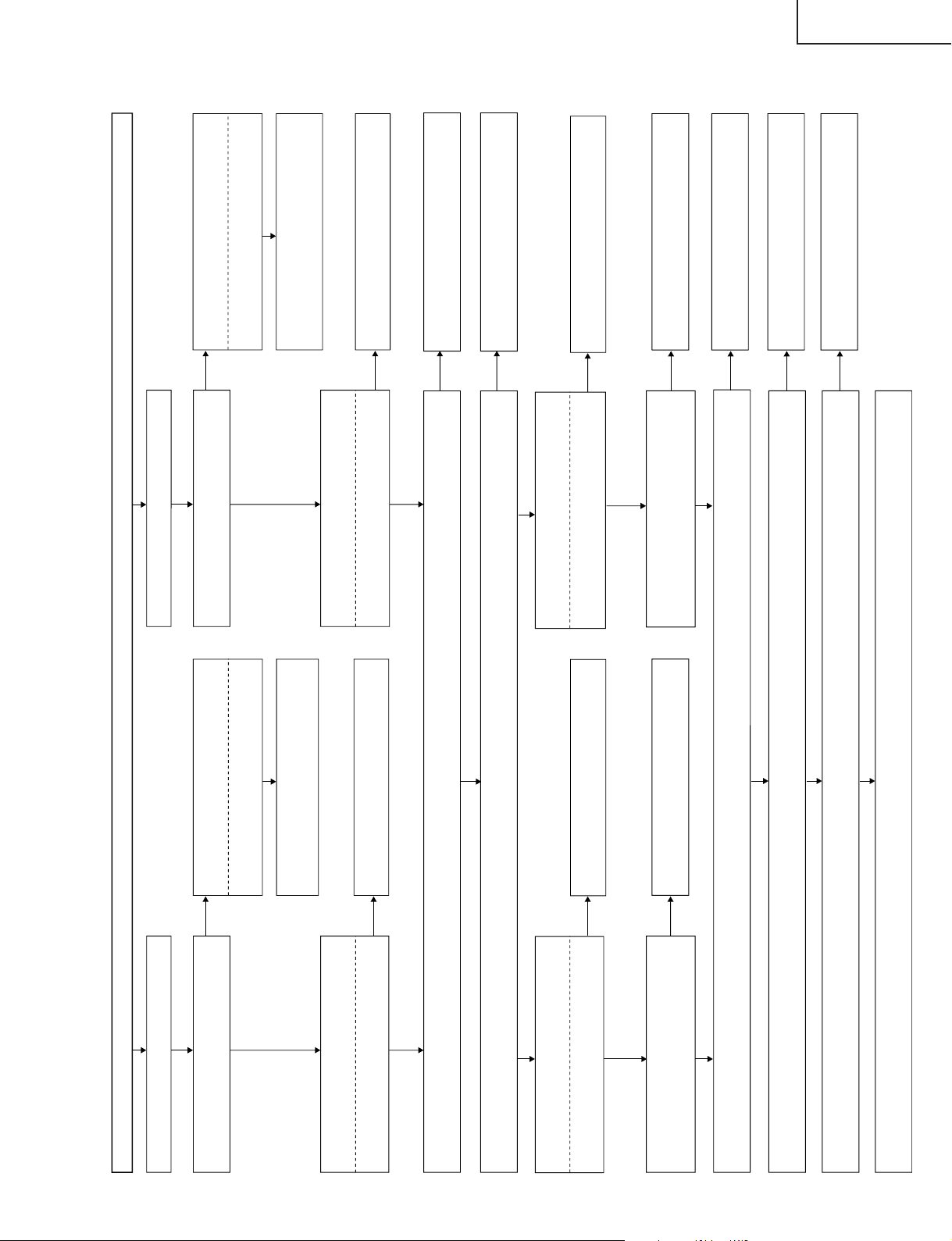
TROUBLE SHOOTING TABLE (Continued)
No video output (1)
External input in trouble <Video 1>
Is Video 1 selected in the input switching
menu screen?
Are there digital video signal outputs at pins
(43), (44), (46), (47), (48), (49), (54), (55)
and (58) of IC400?
Are there digital video signal inputs at pins (51) thru (78) and (7) thru (10) of IC3201? (Signal pins only)
Are there digital video signal outputs at pins (39) thru (49) of IC3201? (Signal pins only)
Are there digital video signal outputs at pins (3) thru (16) of SC3200? (Signal pins only)
<Composite video signal input> Is there main video signal output at pin (60) of IC3800, or sub video signal output at pin (56)?
<Composite video signal input>
Is there signal input at pin (65)?
Is there signal input at each input pin of
IC3800 (AV SWITCH)?
Select Video 1 and the input signal in the input
switching menu screen.
If signal name is in gray and not selectable
in the menu screen
Check between pin (4) of J1103 and pin
(65) of IC3800.
Is composite video signal detection
functioning normally? Check between
J1103 and pin (9) of IC1102.
Is there signal input at each input pin of
IC400 (MAIN VIDEO DEC)?
<Composite video signal input>
Is there signal input at pin (85)?
Check IC 400 (MAIN VIDEO DEC) and its
peripheral circuits.
Check between IC401 and IC400.
External input in trouble <Video 2>
YES
YES
YES
YES
YES
YES
YES
YES
YES
NO
NO
NO
Check between IC501 and IC500.
NO
NO
Are there digital video signal outputs at pins
(43), (44), (46), (47), (48), (49), (54), (55)
and (58) of IC500?
Check IC500 (SUB VIDEO DEC) and its
peripheral circuits.
NO
Replace the main PWB, or check between
IC400/IC500 and IC3201.
NO
Check IC3201 (LV DSTx) and its peripheral
circuits.
Check between IC3201 and SC3200.
NO
NO
Select Video 2 and the input signal in the
input switching menu screen.
If signal name is in gray and not selectable
in the menu screen
Check between pin (8) of J1105 and pin
(71) of IC3800.
Check IC3800 (AV SWITCH) and its
peripheral circuits.
Is composite video signal detection
functioning normally? Check between
J1105 and pin (11) of IC1102.
NO
NO
NO
<Composite video signal input> Is there main video signal input at pin (2) of IC401, or sub video signal input at pin (2) of IC
501?
Check between IC3800 and IC401/IC501.
NO
No problem up to the main PWB. Check TMDS PWB.
Is Video 2 selected in the input switching
menu screen?
<Composite video signal input>
Is there signal input at pin (71)?
Is there signal input at each input pin of
IC3800 (AV SWITCH)?
YES
<Composite video signal> input
<Main video signal>
Is there signal input at each input pin of
IC500 (SUB VIDEO DEC)?
<Composite video signal input>
Is there signal input at pin (85)?
<Sub video signal>
TU-GA1U-S
TU-GAD
27
Page 28
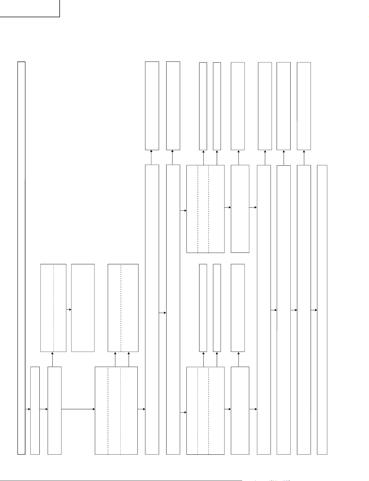
TU-GA1U-S
No video output (2)
External input in trouble <Video 3>
Is Video 3 selected in the input switching
menu screen?
Are there digital video signal outputs at pins
(43), (44), (46), (47), (48), (49), (54), (55)
and (58) of IC400?
Are there digital video signal inputs at pins (51) thru (78) and (7) thru (10) of IC3201? (Signal pins only)
Are there digital video signal outputs at pins (39) thru (49) of IC3201? (Signal pins only)
Are there digital video signal outputs at pins (3) thru (16) of SC3200? (Signal pins only)
No problem up to the main PWB. Check TMDS PWB.
<Composite video signal input> Is there main video signal input at pin (60) of IC3800, or sub video signal input at pin (56)?
<S-video signal input> Are there main Y-signal input at pin (60) and main C-signal input at pin (59) of IC3800, or sub Y-signal
input at pin (56) and sub C-signal input at pin (55)?
<Composite video signal input> Is there main video signal input at pin (2) of IC401, or sub video signal input at pin (2) of IC
501?
<S-video signal input> Are there main Y-signal input at pin (2) and main C-signal input at pin (6) of IC401, or sub Y-signal in
put at pin (2) and sub C-signal input at pin (6) of IC501?
<S-video signal input>
Are there Y-signal input at pin (5) and
C-signal input at pin (7)?
<Composite video signal input>
Is there signal input at pin (3)?
Is there signal input at each input pin of
IC3800 (AV SWITCH)?
Select Video 3 and the input signal in the
input switching menu screen.
If signal name is in gray and not selectable
in the menu screen
Check between pins (2) of J2404 and pins
(3) of IC3800.
Check between pins (3) & (4) of J2401 and
pins (5) & (7) of IC3800.
Is composite video/S-video signals detection
functioning normally? Check between J2404
and pin (12) of IC1102, and between J2401
and pin (6) of IC3800.
Is there signal input at each input pin of
IC400 (MAIN VIDEO DEC)?
<Composite video signal input>
Is there signal input at pin (85)?
<S-video signal input>
Are there Y-signal input at pin (85) and C-
signal input at pin (90)?
Check IC 400 (MAIN VIDEO DEC) and its
peripheral circuits.
Check between IC401 and IC400.
Check between IC401 and IC400.
YES
YES
NO
NO
NO
NO
NO
Check between IC501 and IC500.
Check between IC501 and IC500.
NO
NO
NO
YES
YES
YES
YES
YES
Check IC3800 (AV SWITCH) and its
peripheral circuits.
NO
Check between IC3800 and IC401/IC501.
NO
YES
YES
<Composite video signal / S-video signal> input
<Main video signal>
Are there digital video signal outputs at pins
(43), (44), (46), (47), (48), (49), (54), (55)
and (58) of IC500?
Is there signal input at each input pin of
IC500 (SUB VIDEO DEC)?
<Composite video signal input>
Is there signal input at pin (85)?
<S-video signal input>
Are there Y-signal input at pin (85) and C-
signal input at pin (90)?
Check IC500 (SUB VIDEO DEC) and its
peripheral circuits.
Replace the main PWB, or check between
IC400/IC500 and IC3201.
NO
NO
Check IC3201 (LV DSTx) and its peripheral
circuits.
NO
Check between IC3201 and SC3200.
NO
<Sub video signal>
TU-GAD
TROUBLE SHOOTING TABLE (Continued)
28
Page 29
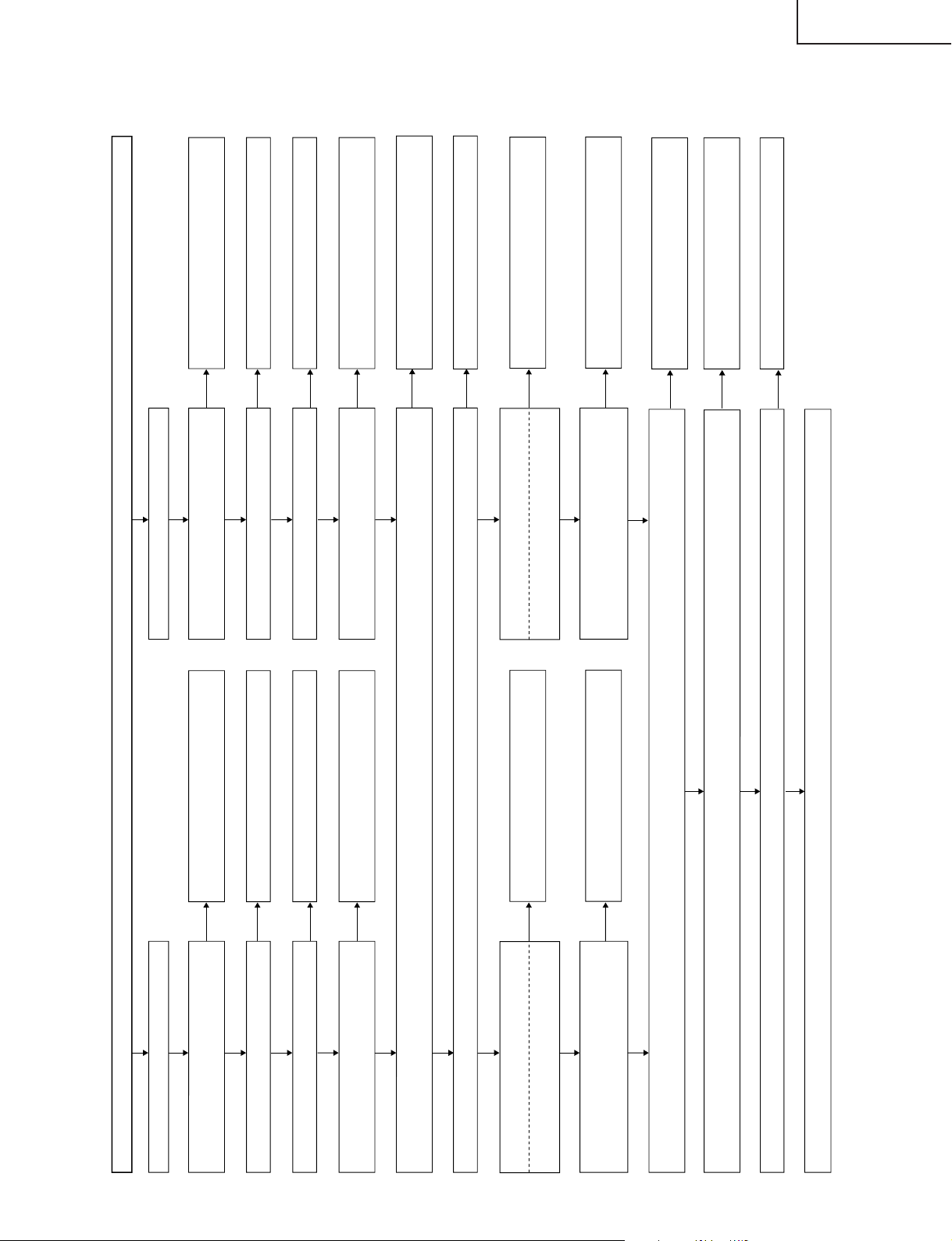
TU-GA1U-S
No video output (3)
Tuner-A (U/V) in trouble
Is there video signal output at pin (17) of
TU1101(video output)?
Is there signal input at pin (7) of IC1103?
Is there signal output at pin (5) of IC1103?
Is there signal input at pin (17) of IC3800
(AV SWITCH)?
Check the tuner and its peripheral circuits.
Check between the tuner and IC1103.
Check IC1103 and its peripheral circuits.
Check between IC1103 and IC3800.
Are there digital video signal outputs at pins
(43), (44), (46), (47), (48), (49), (54), (55)
and (58) of IC400?
Are there digital video signal inputs at pins (51) thru (78) and (7) thru (10) of IC3201? (Signal pins only)
Is there main video signal output at pin (60) of IC3800, or sub video signal output at pin (56)?
Is there main video signal input at pin (2) of IC401, or sub video signal input at pin (2) of IC501?
Are there digital video signal outputs at pins (39) thru (49) of IC3201? (Signal pins only)
Are there digital video signal outputs at pins (3) thru (16) of SC3200? (Signal pins only)
No problem up to the main PWB. Check TMDS PWB.
Is there signal input at each input pin of
IC400 (MAIN VIDEO DEC)?
<Component video Signal Input>
Is there signal input at pin (85)?
Check between IC401 and IC400.
Check IC400 (MAIN VIDEO DEC) and its
peripheral circuits.
NO
YES
YES
YES
YES
YES
YES
YES
YES
YES
YES
NO
NO
NO
Tuner-B (U/V) in trouble
Is there video signal output at (video output)
pin (17) of TU1102?
Is there signal input at pin (1) of IC1103?
Is there signal output at pin (3) of IC1103?
Is there signal input at pin (19) of IC3800
(AV SWITCH)?
Check the tuner and its peripheral circuits.
Check between the tuner and IC1103.
Check IC1103 and its peripheral circuits.
Check between IC1103 and IC3800.
NO
YES
YES
YES
YES
NO
NO
NO
NO
NO
Are there digital video signal outputs at pins
(43), (44), (46), (47), (48), (49), (54), (55)
and (58) of IC500?
Is there signal input at each input pin of
IC500 (SUB VIDEO DEC)?
<Component video Signal Input>
Is there signal input at pin (85)?
Check between IC501 and IC500.
Check IC500 (SUB VIDEO DEC) and its
peripheral circuits.
NO
NO
YES
YES
Check IC3800 (AV SWITCH) and its
peripheral circuits.
NO
Check between IC3800 and IC401/IC501.
NO
<Tuner U/V> input
<Main video signal>
Replace the main PWB, or check between
IC400/IC500 and IC3201.
NO
Check IC3201 (LV DSTx) and its peripheral
circuits.
NO
Check between IC3201 and SC3200.
NO
<Sub video signal>
TU-GAD
TROUBLE SHOOTING TABLE (Continued)
29
Page 30
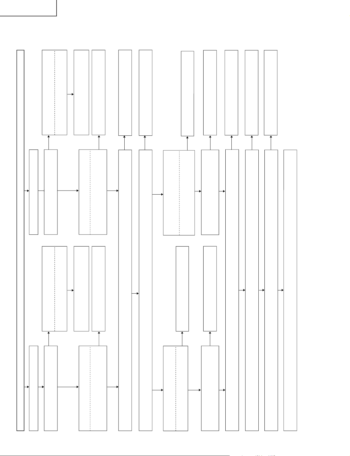
TU-GA1U-S
No video output (4)
External input in trouble <Video 1>
Is Video 1 selected in the input switching
menu screen?
Are there digital video signal outputs at
each output pin (AD_***) of IC3700 (ADC)?
Are there digital video signal inputs at pins (51) thru (78) and (7) thru (10) of IC3201? (Signal pins only)
Are there digital video signal outputs at pins (39) thru (49) of IC3201? (Signal pins only)
Are there digital video signal outputs at pins (3) thru (16) of SC3200? (Signal pins only)
Are there main video signal outputs at pins (46), (48) and (50) of IC3801, sub video signal outputs at pins (40), (42) and (44)
, and pass video signal
outputs at pins (34), (36) and (38)?
<Component video signal input>
Are there signal inputs at pins (53), (55)
and (57)?
Is there signal input at each input pin of
IC3801 (CHROM SWITCH)?
Select Video 1 and the input signal in the input
switching menu screen.
If signal name is in gray and not selectable
in the menu screen.
Check between pins (7), (14) and (20) of
J1103 and each input pin of IC3800.
Is Component signals detection functioning
normally? Check between J1103 and pin
(30) of SC3802.
Is there signal input at each input pin of
IC3700 (ADC)?
Are there signal inputs at pins (5), (13) and
(20)?
Check IC3700 (ADC) and its peripheral
circuits.
Check between IC3703 and IC3700.
External input in trouble <Video 2>
YES
NO
NO
Is Video 2 selected in the input switching
menu screen?
<Component signal input>
Are there signal inputs at pins (5), (7), (9)?
Is there signal input at each input pin of
IC3801 (CHROM SWITCH)?
Select Video 2 and the input signal in the input
switching menu screen.
If signal name is in gray and not selectable
in the menu screen
Check between pins (3), (6), (9), of J1105
and each input pin of IC3801.
Is Component signals detection functioning
normally? Check between J1105 and pin
(76) of IC3800.
YES
YES
YES
YES
YES
YES
YES
YES
NO
NO
Check between IC501 and IC500.
NO
NO
Are there digital video signal outputs at pins
(43), (44), (46), (47), (48), (49), (54), (55)
and (58) of IC500?
Check IC500 and its peripheral circuits.
NO
Replace the main PWB, or check between
IC3700/IC500 and IC3201.
NO
Check IC3201 (LV DSTx) and its peripheral
circuits.
Check between IC3201 and SC3200.
NO
NO
Check IC3801 (CHROM SWITCH) and its
peripheral circuits.
NO
<Main Video Signal> Are there pass signal inputs at pins (1), (5) and (25) of IC3703?
<Sub Video Signal (525I)> Are there sub signal inputs at pins (8), (10) and (13) of IC501?
Check between IC3801 and IC3703, and
between IC3801 and IC501.
NO
No problem up to the main PWB. Check TMDS PWB.
<Component video signal> input
<Main Video Signal>
Is there signal input at each input pin of
IC500 (SUB VIDEO DEC)?
<Sub video signal input>
Are there signal inputs at pins (85), (92)
and (94)?
<Sub Video Signal (525I)>
TU-GAD
TROUBLE SHOOTING TABLE (Continued)
30
Page 31

TROUBLE SHOOTING TABLE (Continued)
DVI Input (Digital PC mode)
TU-GA1U-S
TU-GAD
Are there Rx0, 1, 2 and C signal
inputs to IC1900?
YES
Check PC settings.
Check IC1915 and its
peripheral circuits.
Check IC1917 and its
peripheral circuits.
Are there Hsync, Vsync and RGB
DAC signal outputs from IC1900?
YES
Are there RGB, Hsync and Vsync
signal outputs from ME connector?
YES
NO
NO
NO
Are IC1915 data accessed by I2C
when connected to PC?
NO
YES
Are outputs at pins (12) and (14) of
IC1917 both (H, H)?
NO
YES
Do pins (12) and (14) become (L, L)
when analog AV mode is entered?
NO
YES
Check ME connector I2C signal line.
Check IC1900 and its
peripheral circuits.
Check IC1901, IC1903 and
their peripheral circuits.
Are there RGB, Hsync and Vsync
signal inputs to the main PWB
IC3700 and IC3701?
YES
Check IC3700, IC3701 and their
peripheral circuits.
NO
Check ME harness for
disconnection.
31
Page 32

TU-GA1U-S
TU-GAD
TROUBLE SHOOTING TABLE (Continued)
DVI Input (Analog PC mode)
Are there RGB signal inputs at pins
(25), (26) and (27), and Hsync/Vsync
signal inputs at pins (28) and (8) from
DVI connector?
YES
Check PC settings.
NO
Are IC1915 data accessed by I2C
when connected to PC?
NO
YES
Are outputs at pins (12) and (14) of
IC1917 both (H, L)?
NO
YES
Check IC1915 and its
peripheral circuits.
Check IC1917 and its
peripheral circuits.
Are there Vsync and Hsync signal
outputs at pins (4) and (6) of IC1904?
YES
Are there RGB, Hsync and Vsync
signal outputs from ME connector?
YES
Are there RGB, Hsync and Vsync
signal inputs to IC3700 and IC3701
of the main PWB?
YES
Check IC3700, IC3701 and their
peripheral circuits.
NO
NO
NO
Do pins (12) and (14) become (L, H)
when digital AV mode is entered?
NO
YES
Check ME connector I2C signal line.
Check IC1904 and its
peripheral circuits.
Check IC1901, IC1903 and
their peripheral circuits.
Check ME harness for
disconnection.
32
Page 33

TROUBLE SHOOTING TABLE (Continued)
DVI Input (Digital AV mode)
Are there Rx0, 1, 2 and C signal
inputs to IC1900?
YES
NO
Are IC1911 data accessed by I2C
when connected to PC?
NO
YES
TU-GA1U-S
TU-GAD
Check PC settings.
Check IC1911 and its
peripheral circuits.
Check IC1917 and its
peripheral circuits.
Are there Hsync, Vsync and RGB
DAC signal outputs from IC1900?
YES
Are there RGB, Hsync and Vsync
signal outputs from ME connector?
YES
Are there RGB, Hsync and Vsync
signal inputs to the main PWB
IC3700 and IC3701?
YES
NO
NO
NO
Are outputs at pins (12) and (14) of
IC1917 both (L, H)?
NO
YES
Do pins (12) and (14) become (H, L)
when analog PC mode is entered?
NO
YES
Check ME connector I2C signal line.
Check IC1900 and its
peripheral circuits.
Check IC1901, IC1903 and
their peripheral circuits.
Check ME harness for
disconnection.
Check IC3700, IC3701 and their
peripheral circuits.
33
Page 34

TU-GA1U-S
TU-GAD
TROUBLE SHOOTING TABLE (Continued)
DVI Input (Analog AV mode)
Are there RGB signal inputs at pins
(25), (26) and (27), and Hsync/Vsync
signal inputs at pins (8) and (28) from
DVI connector?
YES
Check PC settings.
NO
Are IC1911 data accessed by I2C
when connected to PC?
NO
YES
Are outputs at pins (12) and (14) of
IC1917 both (L, L)?
NO
YES
Check IC1915 and its
peripheral circuits.
Check IC1917 and its
peripheral circuits.
Are there Vsync and Hsync signal
outputs at pins (4) and (6) of IC1904?
YES
Are there RGB, Hsync and Vsync
signal outputs from ME connector?
YES
Are there RGB, Hsync and Vsync
signal inputs to IC3700 and IC3701
of the main PWB?
YES
Check IC3700, IC3701 and their
peripheral circuits.
NO
NO
NO
Do pins (12) and (14) become (H, H)
when digital PC mode is entered?
NO
YES
Check ME connector I2C signal line.
Check IC1904 and its
peripheral circuits.
Check IC1901, IC1903 and
their peripheral circuits.
Check ME harness for
disconnection.
34
Page 35

TROUBLE SHOOTING TABLE (Continued)
TMDS PWB Check
Are signals supplied to R3111-R3114
and R3116?
YES
NO
Check SC3100 and FFC for
disconnection.
TU-GA1U-S
TU-GAD
Are there Hsync, Vsync, blanking and
clock signal outputs at pins (3), (5),
(6) and (26) of IC3105?
YES
Is pin (13) (reset) of IC3101 in "H"?
YES
Are there signal outputs at pins (1), (2), (9),
(10), (17), (18), (23) and (24) of SC3102?
YES
Check system cables and the
display.
NO
NO
NO
Check IC3105 and its
peripheral circuits.
Check IC3101 and
harness.
Check IC3101 and its
peripheral circuits.
35
Page 36

TU-GA1U-S
TU-GAD
HOW TO UPGRADE THE INTERNAL PROGRAM
The model employs the following software.
» Main software (AVC System)
» Monitor microprocessor software (Display)
» Card microprocessor software
The main software and the monitor microprocessor software can be upgraded by using a general-purpose SD
memory card, while the card microprocessor software by using a PC card. The followings are the procedures for
upgrading, explained separately for each of the main software, the monitor microprocessor software and the card
microprocessor software.
Ë
Main software version upgrade
Get ready before you start
» SD memory card of 8MB or higher capacity
» PC running on Windows 98/98SE/ME/2000/XP operating system
» SD memory card reader/writer with USB connectivity, PC card adapter
» SD memory card formatting software
(Downloadable at http://panasonic.jp/support/audio/sd/download/sd_formatter.html)
Preparations
To upgrade the main software, it is necessary to get ready the SD card for version upgrade before you start.
Follow the steps below and create the SD card for version upgrade.
1 Insert the SD card into the SD card reader/writer. Start the SD card formatting software. Click [Format].
(When you have the drive options, select the drive where the SD card is inserted before you proceed.)
36
Page 37

2 When the formatting is over, the following window appears. Click [OK].
3 Click [Exit] to finish the formatting.
Note : When you are done, take out the SD card once to make sure it is finished, and then insert it again.
TU-GA1U-S
TU-GAD
4 Copy the binary image file KA1UAxxx.SDC (named tentatively) for version upgrade to the root directory
(folder) of the SD card drive.
Note : In the SD card drive, do not put other folders or unrelated files, or more than one binary image files
for version upgrade.
5 Now the SD card for version upgrade is ready.
37
Page 38

TU-GA1U-S
TU-GAD
How to upgrade the software
Software upgrading can be done regardless of whether a dedicated display is connected or not. You can view
the progress on the dedicated display if it is connected. When such display is not used, see the power LED on
the AVC System which blinks according to the status of upgrading. It should be noted that, unlike the digital
model, the progress of upgrading does not appear on the screen of the TV set connected to the video output
terminal of the AVC System.
1 Shut off the AC power to the AVC System (i.e. unplug the AC power cable).
2 Insert the SD card for version upgrade (prepared as above) into the service socket below the CENTER
CHANNEL INPUT terminal in the rear of the AVC System, keeping the cut corner of the SD card at the
right-hand side.
Note : If the SD card is inserted with wrong orientation, the card will go deep inside the set beyond retrieval.
Use due care to insert the SD card correctly.
3 While depressing the SYSTEM RESET button in the front of the AVC System, turn on the AC power (i.e.
plug in the AC power cable).
Note : After the AVC System is started, you may release the SYSTEM RESET button.
4 After the AVC System startup, the system upgrade screen as shown below appears in several to 10-odd
seconds.
<SYSTEM UPGRADE>
Program OK NG
EEPROM
OK NG
12 %
US
5 Even a single failure in the process will trigger the upgrade failure screen as shown below. The word “NG”
changes to red for the item failed.
Note : In the event of a failure, repeat the upgrading process. If the process repeatedly fails, the hardware
failure is likely.
<UPGRADE FAILURE>
Program OK NG
100 %
EEPROM
OK NG
US
Ver 1.07(U 2004/04/01 2)
38
Page 39

TU-GA1U-S
TU-GAD
6 Upon completion of the whole process, the upgrade success screen as shown below appears. You can
check the new software version on this screen. The version information appears after the upgrade is
complete.
<UPGRADE SUCCESS>
Program OK NG
100 %
EEPROM
Ver 1.07(U 2004/04/01 2)
OK NG
US
7 Shut off the AC power to the AVC System (unplug the AC power cable), and remove the SD card for
version upgrade.
8 Now the software version upgrade is complete.
Note : When you are done with the software version upgrade, start the set, go to the top page of the
process adjustment screen and check the main software version information.
Ë
Monitor microprocessor software version upgrade
Get ready before you begin
Get ready the same items as listed in the "Main software version upgrade". In addition, the display unit whose
software is to be upgraded and the AVC System unit should also be ready.
Preparations
Create the SD card for monitor microprocessor software version upgrade in the same manner as explained in
the "Main software version upgrade". Copy the binary image file for monitor microprocessor software version
upgrade to the SD card drive.
How to upgrade the software
The software upgrade is performed in the environment where the AVC System is connected to the display unit
whose software is to be upgraded. During the monitor microprocessor software version upgrade, the progress
of upgrading will appear neither on the display screen nor on the screen of the TV set connected to the monitor
output terminal of the AVC System. The upgrading status is seen by the blinking of the display side power LED
indicator.
1 Connect the display to the AVC System correctly. Turn on the AC power of each unit (plug in the AC power
cable).
2 Turn on the main power switch (not the receiver power switch) of the display beforehand.
3 Shut off the AC power to the AVC System (i.e. unplug the AC power cable).
4 Insert the SD card for version upgrade (prepared as above) into the service socket below the CENTER
CHANNEL INPUT terminal in the rear of the AVC System, keeping the cut corner of the SD card at the
right-hand side.
Note : If the SD card is inserted with wrong orientation, the card will go deep inside the set beyond retrieval.
Use due care to insert the SD card correctly.
39
Page 40

TU-GA1U-S
TU-GAD
5 While depressing the SYSTEM RESET button in the front of the AVC System, turn on the AC power (i.e.
plug in the AC power cable).
Note : After the AVC System is started, you may release the SYSTEM RESET button.
Caution!!
The moment this operation is done, the upgrading process of the monitor microprocessor software
starts. While the upgrade is ongoing, never turn off the power to the display or the AVC System.
Otherwise the upgrade will fail and the system may be damaged seriously beyond recovery
(inability of the display unit startup).
6 After the AVC System startup, the display side power LED starts blinking in green in several to 10-odd
seconds.
7 Wait until the display side power LED stops blinking, the AVC System restarts automatically, and the
normal startup screen appears on the display (it will take 2-3 minutes).
8 Shut off the AC power to the AVC System (unplug the AC power cable), and remove the SD card for
version upgrade.
9 Now the software version upgrade is complete.
Note : When you are done with the software version upgrade, start the set, go to the top page of the
process adjustment screen and check the monitor microprocessor software version information.
Ë
Card microprocessor software version upgrade
1 When the set is turned on, unplug the AC power cable from the outlet for forced shutdown.
2 Insert a new microprocessor software card into the PC card slot.
3 Plug the AC power cable into the outlet.
5 Press the Menu button and select the card mode.
5 The card microprocessor program is automatically loaded from the PC card.
6 When the loading is over, "Finished" message appears.
7 Unplug the AC power cable from the outlet for forced shutdown.
40
Page 41

654321
A
B
C
D
E
F
G
H
CHASSIS LAYOUT
FRONT
AVSUB
DVI TMDS
TU-GA1U-S
TU-GAD
41
Page 42

TU-GA1U-S
TU-GAD
CHASSIS LAYOUT
H
G
F
E
MAIN
PC CARD
D
AV
C
B
A
42
87109654321
Page 43

TU-GA1U-S
TU-GAD
CPU
AUDIO-I/F
43
1716 1918151413121110
Page 44

TU-GA1U-S
2
C
4
0
4
W
/
W
TU-GAD
OVERALL WIRING DIARAM-1/2
H
G
F
E
D
P3804
30P
CPU UNIT
DUNTKC427FE12
QCNW-C030WJPZ:Harness A
QCNW-C030WJPZ:Harness B
AF AD PS
P3805
4P
AV UNIT
DUNTKC663FE01
P5711
2P
P3802
10P
P3803
15P
SC3802
45P
QCNW-C598WJPZ
AH
P5705
8P
MA
QCNW-C011WJPZ:Harness A
MB
QCNW-C011WJPZ:Harness B
FC
QCNW-C014WJQZ
P8506
5P
DU DP
QCNW-C041WJQZ:Harness A
FFC
P8502
9P
MA
MB
FC
SC9302
80P
BtoB
SC2102
80P
P401
10P
P501
15P
SC7200
45P
FRONT UNIT
DUNTKC483DE0
AF
MAIN UNIT
DUNTKC619FE05
P1001
6P
P801
6P
P2402
30P
QCN
P15
1
SH
QCNW-C041WJQZ:Harness B
P5701
60P
P5702
60P
SA
PA
SF
SJ
B to B
B to B
QCNW-C033WJQZ
QCNW-C036WJQZ:Harness B
SC2500
60P
QCNW-C036WJQZ:Harness C
AV SUB UNIT
DUNTKC259FE05
QCNW-C035WJQZ
SC2501
60P
QCNW-C034WJQZ
QCNW-C026WJQZ
Relay
CNA102
8P
CNA101
15P
1-bit AMP
87109654321
P5703
12P
C
B
A
FAN
FAN
P5706
3P
P5707
3P
P3800
5P
P5708
7P
P3801
15P
QCNW-C036
SF SH
P6002
5P
SJ
P6001
7P
AUDIO I
DUNTK
SC
P6003
8P
Audio
MDR
P6
1
DVI
44
Page 45

TU-GA1U-S
TU-GAD
ONT UNIT
NTKC483DE02
P2402
30P
F
QCNW-C031WJQZ
05
P1902
AD
4P
DVI UNIT
DUNTKC267FE15
P1904
2P
AH
P1900
10P
MD ME
QCNW-C018WJPZ:Harness A
QCNW-C018WJPZ:Harness B
MD ME
P3700
10P
P1901
11P
P7200
11P
P1903
12P
MF
QCNW-C018WJPZ:Harness C
MF
P3701
10P
PC CARD UNIT
DUNTKC266FE02
P5003
12P
PC
PP
P7220
2P
P5102
50P
FP
QCNW-C023WJQZ
FFC
FP
SC7201
50P
P1501
14P
SH
QCNW-C036WJQZ:Harness A
JQZ
6002
5P
6001
7P
6003
8P
io
SH
P6000
14P
AUDIO I/F UNIT
DUNTKC484DE02
MDR
DVI
Cable
DU
P3101
5P
SC1500
12P
LP LV
LP LV
SC3101
12P
TMDS UNIT
DUNTKC261FE05
SC3200
FFC FFC
TMDS
33P
SC3100
SC3100
33P
33P
PA
P1752
12P
PB
QCNW-C024WJQZQCNW-C523WJQZ QCNW-C524WJQZ
DP
P1781
9P
P1790
8P
PI PJ
PI PJ
CN901
8P
P1802
6P
QCNW-C025WJQZ
PB
P1703
6P
DC-DC UNIT
P1791
CN902
RDENCA074WJN1
7P
7P
POWER UNIT
RDENCA064WJN1
P1803
20P
PE
PF PG
P1701
12P
P1702
7P
P1751
3P
PK
PK
CN904
3P
To-Display
1716 1918151413121110
45
Page 46

TU-GA1U-S
TU-GAD
OVERALL WIRING DIARAM-2/2
H
G
F
AUDIO IF 25 TC2+ 25 TXOUT- 50 GND
P6000
1 SENCE 1 SENCE 27 TCLK22 VD+5V 2 +5V 28 TCLK2+
3 SMPOW 3 SMPOW 29 GND
4 VD+5VBK 4 +5VBU 30 TD25 GND 5 GND 31 TD2+
E
D
C
B
A
6 RXDO_M 6 RXD 32 GND
7 TXDO_M 7 TXD 33 GND
8 GND 8 GND N0491FJ
9 CCKM 9 CCKM
10 FLASH_W 10 FLASH_W
11 SRST 11 SRST
12 PM_REQ 12 PM_REQ
13 CSEN2 13 CSEN2 P401
14 CSEN1 14 CSEN1 1 Y/VOUT1 1 Y/VOUT2 1 +5V(D1) 1 UR10V
AV SUB 5 COMP1_Y 5 COMP2_Y 5 F_GND 5 BU5V
SC2500
1 GND 1 GND 7 COMP1_Cb 7 COMP2_Cb N0543FJ 7 UR6V
2 GND 2 GND 8 GND 8 GND 8 D_POW
3 SIF 1 3 SIF 1 9 COMP1_Cr 9 COMP2_Cr P1703 9 +3.3V(D)
4 MAIN.R 4 MAIN.R 10 GND 10 GND 10 GND
5 GND 5 GND N0572FJ 11 COMP3_Y NA045WJ 11 GND
6 GND 6 GND 12 GND 12 +3.3V
7 SIF2 7 SIF2 13 COMP3_Cb P1752 13 ADJ1.8V
8 MAIN.L 8 MAIN.L P3802
9 GND 9 GND 1 Y/VOUT1 15 COMP3_Cr NA168WJ 15 ADJ3.3V
10 GND 10 GND 2 GND NA238WJ 16 NC
11 RM 11 RM 3 COUT1 P5703
12 HP_R 12 HP_R 4 GND 1 UR+35V 18 GND
13 GND 13 GND 5 COMP1_Y P3803
14 GND 14 GND 6 GND 1 Y/VOUT2 3 NC 20 AC_DET
15 LM 15 LM 7 COMP1_CB 2 GND 4 GND MA120WJ
16 HP_L 16 HP_L 8 GND 3 COUT2 5 UR+10V
17 GND 17 GND 9 COMP1_CR 4 GND 6 GND DC-DC
18 GND 18 GND 10 GND 5 COMP2_Y 7 UR+6V P1701 TO MAIN (P1803)
19 C1.PLUG 19 C1.PLUG N0572FJ 6 GND 8 GND 1 UR+10V
20 AOUT_R 20 AOUT_R 7 COMP2_CB 9 BU+5V 2 OVP
21 S.MUTE 21 S.MUTE 8 GND 10 GND 3 GND
22 GND 22 GND 9 COMP2_CR 11 +15V 4 GND
23 SCL3_2 23 SCL3_2 10 GND 12 +15V 5 BU+5V
24 AOUT_L 24 AOUT_L 11 COMP3_Y NA168WJ 6 PS_ON
25 SDA3_2 25 SDA3_2 12 GND 7 UR+6V
26 GND 26 GND 13 COMP3_CB 8 D_POW
27 GND 27 GND 14 GND 9 D+3.3V
28 NC 28 NC 15 COMP3_CR 10 GND
29 L.MUTE 29 L.MUTE NA238WJ 11 GND
30 GND 30 GND 12 D+3.3V
31 SRESET 31 SRESET NA051WJ
32 NC 32 NC
33 HP_MUTE 33 HP_MUTE DC-DC
34 GND 34 GND P1790 TO POWER (CN901) DC-DC
35 GND 35 GND 1 S-VCC+15V P1702 TO MAIN (P1803)
36 SPDIF 36 SPDIF 2 S-VCC+15V 1 AC_DET
37 SCL3_3 37 SCL3_3 3 AC_DET 2 EU_D_POW
38 GND 38 GND CPU 4 UR+10V 3 GND
39 GND 39 GND P8502 TO DC-DC (P1781) 5 UR+10V 4 GND
40 GND 40 GND 1 BU+6V 6 UR+10V 5 ADJ3.3V
41 SDA3_3 41 SDA3_3 2 BU+6V 7 PS_ON 6 UR+6V
42 +8V 42 +8V 3 GND 8 BU+5V 7 ADJ1.8V
43 GND 43 GND 4 GND NA047WJ NA046WJ
44 +8V 44 +8V 5 BU+5V POWER
45 GND 45 GND 6 GND CN901
46 +8V 46 +8V 7 VCC(10V)
47 +5V 47 +5V 8 VCC(10V)
48 GND 48 GND 9 GND
49 +5V 49 +5V N0546FJ DC-DC
50 GND 50 GND DC-DC P1791 TO POWER (CN902)
51 +5V 51 +5V P1781 TO CPU (P8502) 1 S-VCC GND
52 BU+5V 52 BU+5V 1 BU+6V 2 S-VCC GND
53 GND 53 GND 2 BU+6V 3 OVP
54 BU+5V 54 BU+5V 3 GND 4 UR-GND
55 GND 55 GND 4 GND 5 UR-GND
56 BU+5V 56 BU+5V 5 BU+5V 6 UR-GND
57 +3.3V(D) 57 +3.3V(D) 6 GND 7 BU-GND
58 +9V 58 +9V 7 VCC(10V) NA046WJ
59 +3.3V(D) 59 +3.3V(D) 8 VCC(10V) POWER
60 +9V 60 +9V 9 GND CN902
TMDS TX TMDS TX TMDS TX
P3101
TO CPU(P8506)
1 D3V3 1 CTL3 1 GND 18 TD1+
2 TXD 2 MON_DET 2 GND 19 TD13 RXD 3 RST_PL 3 TD2+ 20 GND PC CARD
4 GND 4 SDA_A 4 TD2- 21 TCLK1+ P5003
5 GND 5 SCL_A 5 GND 22 TCLK1- 1 10V 1 10V
N0567FJ 6 HOT PLUG 6 TCLK2 23 GND 2 GND 2 GND
DU
CPU 8 SCL_A5 8 GND 25 TC1- 4 GND 4 GND
P8506
TO TMDS TX(P3101)
1 D3V3 10 +3.3V 10 TC2- 27 TB1+ 6 GND 6 I2S_DA_OUT
2 TXD 11 BU+5V 11 GND 28 TB1- 7 I2S_CL 7 GND
3 RXD 12 V5V 12 TB2+ 29 GND 8 NC 8 I2S_DA_IN
4 GND N0532FJ 13 TB2- 30 TA1+ 9 I2SDA_OUT N0570FJ
5 GND 14 GND 31 TA1- 10 GND
N0567FJ 15 TA2+ 32 GND 11 I2SDA_IN P5102
SH
BtoB
MAIN12
P1501
AV3
P5701
TO MAIN (P1501)
N0064CE N0064CE 2 GND 2 GND 2 D_GND 2 OVP
TO AV (P5701)
MA202WJ WA202WJ NA165WJ
SC3101
MAIN12
SC1500
TO AUDIO IF (P6000)
TO AV SUB (SC2500)
TO MAIN (SC1500)
7 GND 7 TCLK2 24 TC1+ 3 3.3V 3 I2S_WS
9 SDA_A5 9 TC2+ 26 GND 5 I2S_WS 5 I2S_CL
LP
FFC
TO TMDS TX (SC3101)
1 V5V 1 GND 1 3.3V 1 3.3V 26 GND
2 BU+5V 2 GND 2 GND 2 3.3V 27 TXOUT1+
3 +3.3V 3 TA1- N0564FJ 3 3.3V 28 TXOUT4 SDA_C_1 4 TA1+ 4 GND 29 GND
5 SCL_C_1 5 GND 5 GND 30 TXOUT0+
6 GND 6 TB1- 6 GND 31 TXOUT07 HOTPLG5 7 TB1+ 7 DOUT 32 GND
8 SCL_C_2 8 GND 8 DIN 33 GND
9 SDA_C_2 9 TC1- 9 GND 34 GND
10 RST_PL 10 TC1+ 10 GND 35 RXIN011 MON_DET 11 GND 11 GND 36 RXIN0+
12 CTL3 12 TCLK1- 12 10V 37 GND
N0532FJ 13 TCLK1+ 13 10V 38 RXIN1-
MAIN1 MAIN3
3 COUT1 3 COUT2 3 +1.8V(D) 3 GND
4 GND 4 GND 4 +1.8V(D) 4 GND
6 GND 6 GND 6 D.GND 6 PS_ON
AV2
SC3100 TOMAIN (SC3200)
16 TA2- 33 GND 12 NC
17 GND N0491FJ N0574FJ N0464FJ
MAIN11
SC3200 TO TMDS TX(SC3100) P7220 TO PC CARD(P5003) SC7201
14 GND 14 10V 39 RXIN1+
15 TD1- 15 GND 40 GND
16 TD1+ 16 PCC_RST 41 RXIN217 GND 17 GND 42 RXIN2+
18 TA2- 18 TXOUT3+ 43 GND
19 TA2+ 19 TXOUT3- 44 RXCLKIN20 GND 20 GND 45 RXCLKIN+
21 TB2- 21 TXCLKOUT+ 46 GND
22 TB2+ 22 TXCLKOUT- 47 RXIN323 GND 23 GND 48 RXIN3+
24 TC2- 24 TXOUT2+ 49 GND
26 GND N0464FJ
TO AV (P3802) P501 TO AV (P3803) P1802 TO DC-DC (1703) P1803 TO DC-DC
MA
TO MAIN (P401)
TO AV (5705)
TO MAIN (P7220)
FFC
LV
14 GND 14 RU6V
MB
AV2
TO MAIN (P501)
DP
PP
MAIN14 MAIN14
To BS-D unit
SC2102
BB 80pin
BS-D 80pin
P9302 MA159WJ
AV3
P5705 TO PC CARD(P5003)
PC
PS
TO MAIN (SC7201)
To-PC-CARD
FP
FFC
TO_PC CARD(P5102)
PB
DC-DC(6P)
DC-DC(12P)
PA
AV3
TO DC-DC (P1752)
2 GND 19 EU_P_POW
PI
POWER
PJ
POWER
MAIN13MAIN13
87109654321
17 GND
PE
PF
PG
46
Page 47

TU-GA1U-S
TU-GAD
AV2
P3804
TO FRONT(P2402)
1 V4_PLUG 1 V4_PLUG
2 V4_Y 2 V4_Y
003) DV I 2 4 V4_C 4 V4_C
)
26 GND 1 GND 21 LED_CARD 21 LED_CARD
27 TXOUT1+ 2 HDMI_Pr 22 CLS_SW 22 CLS_SW
28 TXOUT- 3 GND DVI1 23 BU+5V 23 LED5V
29 GND 4 HDMI_Y P3700
30 TXOUT0+ 5 GND 1 GND 1 GND 25 CARD(G) 25 GND
31 TXOUT0- 6 HDMI_Pb 2 DV1_SR 2 DVI_SR 26 LED_G DENGEN 26
32 GND 7 GND 3 GND 3 GND 27 GND 27 LED_CARD_G
33 GND 8 HDMI_H 4 DV1_SG 4 DVI_SG 28 LED YOYAKU 28 LED YOY AKU
34 GND 9 HDMI_V 5 GND 5 GND 29 LED OSIRASE 29 LED OSIRASE
35 RXIN0- 10 GND 6 DV1_SB 6 DVI_SB 30 POW 30 POW
36 RXIN0+ N0572FJ 7 GND 7 GND NA170WJ NA169WJ
37 GND 8 DV1_H 8 DVI_H
38 RXIN1- 9 DV1_V 9 DVI_V
39 RXIN1+ 10 GND 10 GND
40 GND N0572FJ N1064TA
41 RXIN242 RXIN2+ DVI1
43 GND P7200
44 RXCLKIN- 1 GND 1 GND
45 RXCLKIN+ 2 +5V 2 +5V
46 GND 3 DVI_HPLG 3 DVI_HPLG
47 RXIN3- 4 DVI_SCDT 4 DVI_SCDT
48 RXIN3+ 5 BU+5V 5 BU+5V
49 GND 6 +3V(D) 6 +3V(D)
50 GND 7 GND 7 GND
N0464FJ 8 SCL_B_1 8 SCL_B_1
P1903
TO MAIIN (P3701)
1 GND AV3
2 HDMI_Pr P5711 TO DVI (P1904) P1904
3 GND 1 SPDIF 1 SPDIF 8 V4_V 8 V4_V
4 HDMI_Y 2 GND 2 GND 9 GND 9 GND
5 GND N0564FJ N0564FJ 10 V4_L 10 V4_L
6 HDMI_Pb 11 GND 11 GND
7 GND AV2 DVI1 12 V4_R 12 V4_R
8 HDMI_H P3805
9 HDMI_V 1 PC_L 14 GND 14 GND
10 GND 2 GND 15 HP_R 15 HP_R
11 NC 3 PC_R 16 GND 16 GND
12 NC 4 GND 17 HP_L 17 HP_L
N0574FJ N0566FJ N0464TA 18 5V(A) 18 5V(A)
MAIN4
MF
TO DVI (P1903)
P3701
MAIN14
TO DVI (P1902)
MAIN4
TO DVI (P1900)
TO DVI (P1901)
9 SDA_B_1 9 SDA_B_1
10 HDMI_HPOW 10 HDMI_HPOW
11 HDMI_INT 11 HDMI_INT
N0573FJ N0573FJ
DVI2 6 V4_SPLUG 6 V4_SPLUG
TO AV (P5711)
AH
P1902 TO AV (P3805) 13 HP_PLUG 13 HP_PLUG
1 DVI_L
2 GND
AD
3 DVI_R
4 GND
P1900
TO MAIIN (P3700)
MD
P1901
TO MAIIN ( P7200 )
ME
3 GND 3 GND
5 GND 5 GND
7 V4_S2PLUG 7 V4_S2PLUG
19 GND 19 GND
20 GND 20 GND
24 BS_RST 24 BS_RST
FRONT
P2402
TO AV (SC3800)
AF
LED_G DENGEN
13
3 TO DC-DC
1 UR10V SC7200
2 OVP 1 GND 1 AFT_1 1 GND 1 GND
3 GND 2 D_POW 2 AFT_2 2 GND 2 GND
4 GND 3 I2CEXT 3 AGC_1 3 OPT_CNOUT 3 OPT_CNOUT
5 BU5V 4 FAN_CONT 4 AGC_2 4 DELAY_RST 4 DELAY_RST
6 PS_ON 5 SCL5 5 GND 5 GND 5 GND P5708
7 UR6V 6 SDA5 6 TXD1 6 GND 6 GND 1 SCL5
8 D_POW 7 GND 7 RXD1 7 LED5V 7 LED5V 2 GND
9 +3.3V(D) 8 AVPWB 8 GND 8 I2S_CL 8 I 2S_CL 3 SDA5
10 GND 9 1BIT_PROTECT 9 SDA3 9 GND 9 GND 4 GND
11 GND 10 TEXT_EN 10 SCL3 10 GND 10 GND 5 SP_PLUG
12 +3.3V 11 CSEN2 11 SDA_A 11 NC 11 NC 6 GND
13 ADJ1.8V 12 GND 12 SCL_A 12 I2S_WS 12 I2S_WS 7 MON1_DOW
14 RU6V 13 SH_ON 13 GND 13 NC 13 NC NA046WJ
15 ADJ3.3V 14 SH_VCC 14 LED_R 14 GND 14 GND
16 NC 15 GND 15 MONI_DOWN 15 NC 15 NC AUDIO IF
17 GND 16 C1_PLUG 16 HPMUTE 16 I2S_DA_OUT 16 I2S_DA_OUT P6001
18 GND 17 SP_PLUG 17 LMUTE 17 GND 17 GND 1 SCL5
19 EU_P_POW 18 4586_INT 18 GND 18 GND 18 GND 2 GND
20 AC_DET 19 GND 19 FAST_SW1 19 BS_SPDIF 19 BS_SPDIF 3 SDA5
MA120WJ 20 SRESET 20 BS_RST 20 I2S_DA_IN 20 I2 S_DA_IN 4 GND
E
PF
C 22 GND 22 TV_COL1 22 GND 22 GND 6 GND
1 TO MAIN (P1803) 23 TV_COL25 23 TV_COL2 23 GND 23 GND 7 MONI_POW
1 UR+10V 24 TV_COL15 24 GND 24 I2S_DA _IN2 24 I2S_DA_IN2 NA061WJ
2 OVP 25 GND 25 SSYSTEM 25 NC 25 NC
3 GND 26 BS_RST 26 SRESET 26 GND 26 GND
4 GND 27 FAST_SW1 27 GND 27 NC 27 NC
5 BU+5V 28 GND 28 SDA_INT 28 CENT_SP_IN 28 CENT_SP_IN AUDIO IF 1bit amp
6 PS_ON 29 L.MUTE5 29 SP_PLUG 29 GND 29 GND P6003 TO 1BIT CNA102
7 UR+6V 30 HP_MUTE5 30 C1_PLUG 30 GND 30 GND 1 RCH(+) 1 Rch +
8 D_POW 31 MONI_DOWN 31 GND 31 GND 31 GND 2 RCH(+) 2 Rch +
9 D+3.3V 32 LED_R 32 SH_VCC 32 SDA_IN 32 SDA_IN 3 RCH(-) 3 Rch 10 GND 33 GND 33 SH_ON 33 GND 33 GND 4 RCH(-) 4 Rch 11 GND 34 SCL_A 34 GND 34 GND 34 GND 5 LCH(-) 5 Lch 12 D+3.3V 35 SDA_A 35 CSEN2 35 GND 35 GND 6 LCH(-) 6 Lch -
NA051WJ 36 SCL_B 36 TEXT_EN 36 MONI_DOWN 36 MONI_DOWN 7 LCH(+) 7 Lch +
PG
C 39 RXD1 39 GND 39 NC 39 NC
2 TO MAIN (P1803) 40 TXD1 40 SDA5 40 SP_PULG 40 SP_PULG AUDIO IF
1 AC_DET 41 GND 41 SCL5 41 NC 41 NC P3800
2 EU_D_POW 42 AGC_2 42 FAN_CONT 42 GND 42 GND 1 SP_SW 1 SP-SW
3 GND 43 AGC_1 43 I2CEXT 43 NC 43 NC 2 1B_RELAY 2
4 GND 44 AFT_2 44 D_POW 44 SDA5 4 4 SDA5 3 GND 3 GND
5 ADJ3.3V 45 AFT_1 45 GND 45 GND 45 GND 4 +5V 4 +5V C
6 UR+6V N0493FJ N0493FJ 46 SCL5 46 SCL5 5 GND 5 GND
7 ADJ1.8V 47 NC 47 NC N0567FJ N0564TA
NA046WJ 48 GND 48 GND
MAIN14
TO AV (SC3802)
FFC
21 SSYSTEM 21 GND 21 GND 21 GND 5 SP_PLUG
37 SDA_B 37 PROTECT 37 NC 37 NC 8 LCH(+) 8 Lch +
38 GND 38 AVPWB 38 GND 38 GND N0864TA N0863TA
DC-DC P5706
P1751 TO POWER (CN904) 1 FAN5V 50 GND 50 GND P3801 TO 1BIT CNA101
1 DC+9V OUT 2 FAN_LOCK 51 GND 51 GND 1 PGND 1 PGND
2 GND 3 GND 52 GND 52 GND 2 PGND 2 PGND
3 PLG_CK N0378GE 53 NC 53 NC 3 PVDD 3 PVDD
PK
POWER 55 NC 55 NC 5 DGND_AD 5
CN904 TO DC-DC (P1751) 5 6 GND 56 GND 6 D+5V 6 D+5V
1 DC+9V OUT 57 GND 57 GND 7 PROTECT 7 PROT ECT
2 GND 58 NC 58 NC 8 MUTE 8 MUTE
3 PLG_CK 59 GND 59 GND 9 RESET 9 RESET
AV2 AV3
SC3802 TO MAIN(SC7200) P5702
FC
AV3
TO FAN1 49 NC 49 NC 1bit amp
To-FAN
AV3
P5707 TO FAN2 60 GND 60 GND 10 AGND_AD 10 AGND_AD
1 GND WA202WJ MA202WJ 11 A+5V 11 A+5V
2 FAN_LOCK 12 RST/PDN 12 RST/PDN
3 FAN10V 13 LCH-IN 13 Lch_IN
N0378GE 14 AGND 14 AGND
To-FAN
TO AV SUB (SC2501)
54 GND 54 GND 4 PVDD 4 PVDD
BtoB
AV SUB
SC2501
TO AV (P5702)
AV3
TO AUDIO IF (P6001)
SJ
TO AV3 (P5708)
AV2
TO AUDIO IF (P6002)
AV2
15 RCH-IN 15 Rch_IN
NA238WJ N1563TA
SC
P6002
SF
SA
1B-RELAY
DGND_AD
TO AV(P3800)
1716 1918151413121110
47
Page 48

TU-GA1U-S
C
8
C
CN
T
W
l
W
TU-GAD
MAIN BLOCK DIAGRAM
AV
H
G
F
U/V-TUNER
U/V-TUNER
INPUT 1
(Component)
INPUT 2
(Component)
INPUT 3
(FRONT)
MONITOR
OUT
TU1101
TU1102
SIF_1
SIF_2
YCVBS
YPbPr(Comp)
CVBS
YPbPr(Comp)
YCVBS
MONITOR_LR
E
PC_ANALOG
(HDMI)
IC1911
24LC21
EEPROM
for AV
PC_DIGITAL
ANALOG_HV
PC_L/R
IC1915
24LC21
EEPROM
for PC
IC1913
24LC2B
EEPROM
for
HDMI
INPUT 5
(DVI-I)
INPUT 4
D
UNIT
IC1912
SII9993
HDMI Receiver
AV SUB
UNIT
CVBS
DVI
UNIT
TUNER
MONITOR
C
CENTER SP
INPUT
HEAD PHONE
MONO_IN
HDMI_SPDIF
IC2710
AK5381
ADC
IC2502
BH3544F
Head Phone
AMP
IC3800
MM1630AQ
AV SWITCH
Tuner_1
TV IN
Tuner_2
TV IN
V
V
V
Y/C
S/S2
MM1519XQ
COMPONENT
INPUT1
V1
INPUT2
D1
INPUT3
D2
IC1900
SII907
DVI HDCP
SIF_1
SIF_2
SC1_Out
MONITOR MAIN
I2S
RX1
TX
DAC
Video_1
Video_2
Video_3
IC3805(Lch)
IC3812(Rch)
BU4051FV
AUDIO SW
IC3801
SWITCH
HDMI_YCbCr
HDMI_HV
IC2501
MSP3440
SC4_IN
D/A
IC2702
AK4586VQ
A/D DIR DAC
HV
MSP
Monitor
Out
Pass
Out
SC2_Out
TV
Main
Out
Main
Out
Sub
Out
SC1_IN
TV
Sub
Out
RGB SELECTOR
I2S_IN
A/D
I2S
RX2
DAC
Main_Y/V
Main_C
Sub_Y/V
Sub_C
MONITOR_CVBS
Main_L/R
Ycomp/Main
CbCr/Main
Ycomp/Sub
CbCr/Sub
Ycomp/Pass
CbCr/Pass
IC1901
AD8185
HV Sel.T
7WH123
MAIN_LR
IC2706
A899WJN1
EEPROM
IC2700
NJU26150
SOUND DSP
I2S
TX
SOUND DIT
IC2504
NJM4565
IC2709
AK4353
IC2701
NJU26106
VIRTUAL
DOLBY
I2S
I2S
Sub_Y/V
Sub_C
CbCr/Sub
Ycomp
DVI_HV
MAIN
UNIT
IC401
SM5313
IC501
SM5313
IC3703
SM5301
IC3704
TA1318AF
SYNC Sepa.
Comp
IC3701
TVHC153T
SYNC Sel
IC2102
EEPROM
BR24L64F
LPF
LPF
LPF
IC801
IXA859
SD IN1
SD IN2
AD/DVI/HDMI
IN
Diginta
Video S
I
A
IC400
Y/V
TC90A92A
3D-YC&Chroma
C
CbCr
TC90A92A
Y/V2
3D-YC&Chroma
C
CbCr
RGB
AD9888
IN_1
IN_2
H_SYNC
IC1105
M62320
COMPONENT
Comp
_V
_H
(Main)
IC500
(Sub)
IC3700
A/D
Main_YC 8bit
Main_HV
Main_CLK
Sub_YC 8bit
SUB_HV
Sub_CLK
YCbCr/RGB
24/48bit
AD_CLK
AD_H
AD_V
B
CN To DIGITAL UNIT
UART
I2C
IC8301/03
A995WJ
SDRAM
256Mb*2
IC8101
A817WJ
Main CPU
A
CPU
UNIT
Cont
rol
IC8302
LHF64FA3
FLASH
SLOW
BUS
A948WJ
IC8201
CPLD
IC8401
TC6384AF
SD Cont
SD
CARD
UART
o
TMDS
FRONT
UNIT
87109654321
48
Page 49

TU-GA1U-S
TU-GAD
it
it
RGB
it
K
_V
SD IN1
SD IN2
AD/DVI/HDMI
IN
IC801
IXA859WJ
Digintal
Video SW
MAIN
OUT
SUB
OUT
CARD IN
CARD
OUT
YPbPr/RGB
24/48bit
HD1,2/VD/CLK
YPbPr/24bit
HD/VD/CLK
YPbPr 8bit
HD/VD/CLK
YPbPr 8bit
HD/VD/CLK
IC7204
DS90CF386
LVDS Rx
IC7205
DS90C385
LVDS Tx
MAIN
SUB
IC3300
IXA091WJ
CVIC
OUT
RGB 24bit
IC3201
LVD823
LVDS Tx
IC3400-03
IXA312WJ
SDRAM
512k*32*4BANK
83.57MHz
Xtal
25.175MHz
Xtal
IC3105
LVD84B
LVDS Rx
RGB
IC3101
24bit
SII170B
TMDS
UNIT
IC3104
UPD4721G
RS232C
Rx/Tx
TMDS Tx
PC CARD
UNIT
TMDS
RS-232C
CARD_UNIT
I2S
IC1001
A869WJN1
CPLD
AUDIO I/F
UNIT
I2C
UART
OUT
IN
Tr.D,C/R
circuit
RY6000-01
SPEAKER
RELAY SW
1-bit AMP.
UNIT
1bit AMP_UNIT
POWER
UNIT
POWER_UNIT
MAIN SP
OUT
EXT-SPEAKER
OUTPUT
MDR
49
CN To AV
CN To DIGITAL
CN To POWER
1716 1918151413121110
Page 50

TU-GA1U-S
R
E
1
U
0
M
SBDAT[15:0]
A
TU-GAD
CPU BLOCK DIAGRAM
H
P8801(N0569FJ)
: Digital Audio out
to AV
P9301
(N0567FJ)
: PC IF
to TMDS
P9001
(N0574FJ)
: B-CAS IF
to B-CAS
P8901
(NA102WJ)
: Analog Rec A/V out
to AV
P9751 (N0545FJ) : Power
LNB_PWR
G
(PQ1CZ41H)
5V(580mA)
BU5V(64mA)
IC9752
(TPS54350)
2.55V(720mA)
A5VT,
30V
Gen
(2mA)
A30V
SC5V
IC9755
(PQ1M335M)
3.3V(60mA)
A3V3
F
E
VCC(10V , 1.15A)
IC9702
D2V5
IC9756
(PQ015EZ1)
1.5V(344mA)
T1V5
*current : typical
IC9751
(PQ1CZ41H)
3.3V(480mA)
D3V3AV5V,
(TPS54350)
1.58V(1150mA)
(PQ0QDZ1U)
IC9701
D1V5
IC9754
9V(32mA)
AV9V
ICC_DRV_RES ,
N_GATEON
AUDMCLK
I2SDATA,SPDIF,I2SCLK,I2SLRCLK,
AMCLK
ASDO1,ASDO4,ABCKO,ALRCKO
ICC_CMD_VCC,
ICC_CLKDIV2,
ICC_DEFFSET
I2CSCL0,I2CSDA0
I2CSCL0,
I2CSDA0
I2CEXT
(BR24L64F)
: EP ROM
IC8453
64Kbit
UATXD1
LOUT_SUB,
ROUT_SUB
AMP
/MUTE
L/R
IC8801
(AK4363VF)
: Audio-DAC
V_SUB
SY_SUB,SC_SB
IC8902
(TK15430V)
: Filter 6MHz
N_AUDIORST
DC_SUB
VCR
S level
AUDMUTE
VCRS1SEL[1:0]
Level
REC_MUTE
Y,C
(TK15420)
STCCLKO,ASDO0,
ABCKO ,ALRCKO
AMCLK
Cont
IC8901
AMP
VCRYO
VCRCO
N_COLD
N_RES
SBDAT[
N_SB
D
T_SYNC_INT
INTCN_T,
INTTMCC_T
C
INTCN_1B,
INTTMCC_1B,
TS0_EN,
TU8001
(SA007WJ)
: BS Tuner
INTEWS_1B
N_UARTS0
MDM_TXD0
N_MDMRST
MDM_DTR
MDM_DCD
IC9601
(A700WJ)
B
: HS Modem
28.22
MHz
TS1_PKTSYNC,
20.467
MHz
TS1_CLK,
TS1_ERR,
TS1_EN,
TS1_DATA
IC8053
(A554WJ)
: OFDM
N_DEMORST
TS0_PKTSYNC,
TS0_DATA
I2CSCL0,I2CSDA0
TS0_CLK,
TS0_ERR,
IC9602
AGC_IF
TU8051
(TA008WJ)
: T Tuner
SDA_T,
SCL_T
(A701WJ)
: DAA
AGC_RF,
IF_OUT_T
J9601
A
(Z1050CE)
: Modem
Con
N_T_INT
N_BS1_INT
BS1_SYNC_INT
N_SBACK
SD_MCLK
SBADD[8:1],N_SBOE,N_SBWE
N_SD_RST,N_SDCS
SBDAT[15:0]
IC8701
(TC6384AF)
: SD Card Control
SC8701
(ZA050WJ)
: SD Card
Slot
SD_PWR
N_FLCS2,N_FLOE,FLADD22,N_FLRST
SBADD[21:1],N_SBWE
SBDAT[15:0]
IC8454
(LHF64FA3)
: Flash 64Mbit
SBADD[21:1],N_SBWE
FL_VPP0
N_FLCS[1:0],N_FLOE,FLADD22,N_FLRST
IC8451
(LHF12F
: Flash 128
87109654321
50
Page 51

out
EL[1:0]
Level
Cont
REC_MUTE
IC8901
(TK15420)
AMP
CLKO,ASDO0,
KO,A LRCKO
AMCLK
VCRYOUT,
VCRCOUT
N_COLDRST,
N_RESET
SBDAT[15:0]
N_SBACK
VIDINDATA[7:0],
VIDINCBCR[7:0],
VIDINCLK,
VIDINH,
VIDINV
Video
RST
DigitalVide
o
In/Out
Rec
Out
Audio
Out
Slow Bus
P9201 (MA160WJ)
:Digital Video in/out IF to MAIN
DOUTY[9:2],DOUTPB[9:2],
DOUTCLK,HDOUT,VDOUT
X8202
STC0PWM
27MHz
IC8201
(A569WJ)
IC8202
(A570WJ)
: CLK-Gen
: CLK-Gen
DCLKI54M,
STC0CLKI,
DCLKI74M
STC/ PLL
IC8101 (A896WJ)
: CPU & AV Decoder
CPLD_INT
TUNER_INT
IRQ[0~5]
N_INTA
N_MAIN_INT[1:0]
N_LINK_IRQ
N_SRESET
I2CSCL1,I2CSDA1
I2CSCL0,I2CSDA0,
PIO
I2C
UAR
T[0~3
]
DDR
IF
N_GATEON
N_SBCE7,
N_SBWE,N_SBOE
LED
*2
UARXD0,
N_UACTS0
UARXD1
UARXD2
UARXD3
SDMD[63:0],
SDDQS[7:0]
SDAD[12:0],SDCLK[1:0],
SDBCLK[1:0],SDCKE,
N_SDCS0,N_SDRAS,
N_SDCAS,N_SDWE,
SDDM[7:0],SDBA[1:0]
P9302 (MA159WJ)
:Main Bus IF to MAIN
SBDAT[15:0]
SBADD[25:1],SBCLK0
N_HOST_CE1
N_SRESET,
RS_ON
TXD,
RXD
SW
UATXD2
UATXD3
IC8301~8304
(A221WJ)
: DDR SDRAM
256Mbit * 4
LNBCONT
UATXD_A,
UARXD_A
TMPOUT
I2CEXT
thermistor
I2CSCL0_B,
I2CSDA0_B,
I2CSCL1_B,
I2CSDA1_B
SW
N_FPI2CEN
I2CSCL0,
I2CSDA0,
I2CSCL1,
I2CSDA1
TU-GA1U-S
TU-GAD
N_EXT_RST
SBDAT[15:0]
54
FA3)
4Mbit
SBADD[21:1],N_SBWE
FL_VPP0
N_FLCS[1:0],N_FLOE,FLADD22,N_FLRST
SBDAT[15:0]
IC8451
(LHF12F01)
: Flash 128Mbit
N_PCIRST
ICC_INT
N_SD_INT
PCI Bus
MDM_RXD0
UATXD0
VM_SDI_RXD0
IC9101
(A885WJ)
: CPLD
CLK33M,
USBCLK48M
SBDAT[7:0]
N_SBACK
TS0 TS1 TS2
CLK
CLK33MB
SBCLK1,N_SBWE,N_SBOE
SBADD[24:21,5:1], N_SBCE[7:4,1:0],
N_EXT_BOOT,
EXT_RDY,
CBOOTS,
PM_REQ
N_SRESET
Reset
IC
TS2CLK,TS2ERROR,
TS2VALID,
TS2SYNC,TS2DATA
N_SBACK
SBDAT[15:0]
N_SBCE3,N_SBOE,
N_LINK_STANDBY
N_SBWE,SBADD[15:1]
IC8501
(MN864610)
: IEEE1394 Link
N_PHY_RESET
LINK_POWER
IC8504
(1782GE)
: PHY
J8502,J8501 (Z1055CE)
: i-LINK Con
TSOU
T
TSOUTCLKO,
TSOUTVALID,
TSOUTSYNC,
TSOUTDATA[7:0]
N_LINK_RESET
24.576
MHz
PCIAD[31:0],PCICKO,
N_FRAME,N_GNT0,N_DEVSEL,
N_REQ0,N_CBE[3:0],N_TRDY,
N_STOP,N_PERR,N_PME,IDSE
PAR,N_IRDY,N_SERR
N_FONTCS,N_FLOE
SBADD[22:1],N_SBOE
SBDAT[15:0]
IC8601(A360WJ)
: Font ROM
64Mbit
25
MHz
(A751WJ)
: Ether Cont
(ZA013WJ)
: Ether Con
IC9802
J9801
L,
N_PCIRST
N_VM_CS,VM_CLK,VM_SDO_TXD0,N_VM_NMI
VM_SDI_RXD0,N_VM_BUSY
IC9003
(A911WJ )
:V-MOUSE
4MHz
J9001(A0054CE)
: V-mouse
1716 1918151413121110
51
Page 52

TU-GA1U-S
TU-GAD
POWER BLOCK DIAGRAM
H
AC POWER SUPPLY
CN701 F701 L701 L702 L705 F702 D704 T701 L901 IC901,902
AC(L)
AC(N)
1 LINE LINE LINE BRIDGE SWITCING CHOKE COIL BU+5V
2 FILTER FILTER FILTER RECTIFIER TRANS REGULATER
AVC MAIN POWER
RY701
IC701
AC-DC PC701
CONTROLLLER VOLTAGE
Q701,702 PC702 Q901
RELAY DRIVE RELAY DRIVE PS_ON
TRANSISTOR CONTROL
FEED BACK
D901
(BU+5V)
(PS_ON)
D708 L703 L704 T702
G
BRIDGE
RECTIFIER
F
CHOKE COIL
PFC CONVERTOR SWITCING
TRANS D709 TRANS
IC702 Q705 TEMPERATURE FUSE MOS-FET
PFC CONTROL MOS-FET
IC
PC705 Q905,906
AC DETECTOR AC DETECTOR
D913 TRANSISTOR
F703 Q706
IC703 PC703
AC-DC VOLTAGE
CONTROLLLER FEED BACK
PC704
O.V.P.
PROTECTOR
AVC SUB POWER
(UR+10V)
P1790 IC1706 ZD1708
E
D
S-VCC +15V
S-VCC +15V
AC_DET
UR+10V
UR+10V
UR+10V
PS_ON
BU+5V
P1791 1CH UP D1706
S-VCC GND 1 Q1702 L1704
S-VCC GND 2 OUT2 4PIN MOS-FET
O.V.P. 3 D1717 D1704
UR GND 4
UR GND 5 Q1701 L1703
UR GND 6 OUT1 2PIN MOS-FET CHOKE COIL
BU GND 7 D1702
PI UR+10V L1707 D1711 ZD1705
1
2
3 L1701 D1701 Q1705
4
5
6 Q1704 L1706
7 3PIN PVCC1(CH1,2) OUT4 9PIN MOS-FET
8 8PIN PVCC2(CH3,4,5) IC1701 D1708
PJ
CHOKE COIL
32PIN VCC OUT5(UP) 12PIN MOS-FET
5CH SWITHING REGULATER
CONTROLLER Q1703 L1705
4CH DOWN OUT3 7PIN MOS-FET CHOKE COIL
REGULATER
CHOKE COIL D1712
STB1 48PIN
ON/OFF
STB2,3 47PIN
LOGIC
STB4 46PIN
STB5 45PIN
(UR+35V)
CHOKE COIL
CHOKE COIL
C
IC951 L951
DC-DC CHOKE COIL
B
A
CONVERTER ZD951
Q951
ON/OFF
CONTROL
IC952 L952
DC-DC CHOKE COIL
CONVERTER ZD952
Q954
ON/OFF
CONTROL
D952
D956
D953
D957
87109654321
52
Page 53

TU-GA1U-S
)
TU-GAD
2
(BU+5V)
TER
(PS_ON)
L PI
T702 L902 4
SWITCING
TRANS 6
T MOS-FET
PC703
VOLTAGE DRIVER ZD904
FEED BACK 3
PC704
O.V.P. Q904 D911 7
PROTECTOR
0V)
5V)
L1706 Q1719 9
CHOKE COIL
D1708 ZD1704 D1710 11
COIL P1751
L1704 2
CHOKE COIL
D1717 D1704 ZD1702
COIL 1
COIL 5
ZD951 6
D953 7
D903
Q902 L904 Q907 L903 8
IC904 IC903 IC905 Q907 ZD905 PJ
SYNCRONOUS RECTIFY REGULATER
DIGITAL TRANSISTOR
O.V.P. DETECTOR
(BU+5V)
(S-VCC)
IC1704 6
FET SW 7
MOS-FET 10
D1709 12
ZD1703 PK
D1707 1
D1705 P1701
ZD1701 2
D1703 3
D912
CHOKE COIL
CHOKE COIL
(PLG_CK)
(DC+9V OUT)
(D+5V)
(D+3.3V)
(D+1.8V)
(D_POW)
(PS_ON)
(CPU10V)
(O.V.P.)
MOS-FET (HIGH-SIDE)
SYNCRO-BACK TYPE MOS-FET (LOW-SIDE) D915 1
REGILATER CONTROL
IC906 D916 4
COMPARATOR 5
SHUT-DOWN CONTROL
CHOKE COIL
(S-VCC +15V
(UR+10V)
(O.V.P.)
CN904
PK
DC+9V OUT
1
GND
2
PLG_CK
3
CN901
S-VCC +15V
1
S-VCC +15V
2
AC_DET
3
UR+10V
UR+10V
5
UR+10V
PS_ON
7
BU+5V
CN902
S-VCC GND
S-VCC GND
2
O.V.P.
UR GND
UR GND
UR GND
6
BU GND
P1752
PA TO AV
UR+35V
1
GND
2
NC
3
GND
4
UR+10V
5
GND
UR+6V
GND
8
BU+5V
S-GND
S-VCC
S-VCC
DC+9V OUT
GND
PLG_CK
3
PF TO MAIN
UR+10V
OVP
GND
GND
4
BU+5V
5
PS_ON
6
UR+6V
7
D_POW
8
D+3.3V
9
GND
10
GND
11
D+3.3V
12
P1703
PB TO MAIN
D+5V
1
GND
2
D+1.8VCV
3
D+1.8VCV
4
GND
5
GND
6
P1702
PG TO MAIN
AC_DET
1
NC
2
GND
3
GND
4
ADJ3.3V
UR+6V
ADJ1.8V
CN903
TO
AVC MAIN POWER
COIL MOS-FET
ZD952 P1781
D957 DP TO CPU
Q952
Q953 1
ON/OFF 2
CONTROL 3
(UR+6V)
(D_POW)
1716 1918151413121110
53
4
5
6
7
8
9
NC
NC
GND
GND
BU+5V
GND
CPU10V
CPU10V
GND
Page 54

TU-GA1U-S
TU-GAD
DESCRIPTION OF SCHEMATIC DIAGRAM
VOLTAGE MEASUREMENT CONDITION:
1. Voltages at test points are measured on exclusive
AC adapter or the stable supply voltage of AC 110240V. Signals are fed by a color bar signal generator
for servicing purpose and the above voltages are
measured with a 20k ohm/V tester.
INDICATION OF RESISTOR & CAPACITOR:
RESISTOR
1. The unit of resistance “Ω” is omitted.
(K=kΩ=1000 Ω, M=MΩ).
2. All resistors are ± 5%, unless otherwise noted.
(J= ± 5%, F= ± 1%, D= ± 0.5%)
3. All resistors are 1/16W, unless otherwise noted.
4. All resistors are Carbon type, unless otherwise
noted.
C : Solid
S : Oxide Film T : Special
N : Metal Coating
CAPACITOR
1. All capacitors are µF, unless otherwise noted.
(P=pF=µµF).
2. All capacitors are 50V, unless otherwise noted.
3. All capacitors are Ceramic type, unless otherwise
noted.
(ML): Mylar (TA): Tantalum
(PF): Polypro Film (ST): Styrol
W
: Cement
CAUTION:
This circuit diagram is original one, therefore there may be a
slight difference from yours.
IMPORTANT SAFETY NOTICE:
PARTS MARKED WITH “å” ( ) ARE
IMPORTANT FOR MAINTAINING THE SAFETY OF
THE SET. BE SURE TO REPLACE THESE PARTS
WITH SPECIFIED ONES FOR MAINTAINING THE
SAFETY AND PERFORMANCE OF THE SET.
AVIS DE SECURITE IMPORTANT:
LES PIECES MARQUEES “å” ( )SONT
IMPORTANTES POUR MAINTENIR LA SECURITE
DE L'APPAREIL.
NE REMPLACER CES PIEDES QUE PAR DES
PIECES DONT LE NUMERO EST SPECIFIE POUR
MAINTENIR LA SECURITE ET PROTEGER LE BON
FONCTIONNEMENT DE L'APPAREIL.
54
Page 55

654321
A
B
C
D
E
F
G
H
TU-GA1U-S
TU-GAD
SCHEMATIC DIAGRAM
Ë
FRONT Unit
55
Page 56

TU-GA1U-S
TU-GAD
Ë
AV SUB Unit-1/2
H
G
F
E
D
C
B
A
87109654321
56
Page 57

TU-GA1U-S
TU-GAD
57
1716 1918151413121110
Page 58

TU-GA1U-S
TU-GAD
Ë
AV SUB Unit-2/2
H
G
F
E
D
C
B
A
87109654321
58
Page 59

TU-GA1U-S
TU-GAD
59
1716 1918151413121110
Page 60

TU-GA1U-S
TU-GAD
Ë
TMDS Unit
H
G
F
E
D
C
B
A
87109654321
60
Page 61

TU-GA1U-S
TU-GAD
61
1716 1918151413121110
Page 62

TU-GA1U-S
TU-GAD
Ë
PC CARD Unit-1/4
H
G
F
E
D
C
B
A
87109654321
62
Page 63

TU-GA1U-S
TU-GAD
63
1716 1918151413121110
Page 64

TU-GA1U-S
TU-GAD
Ë
PC CARD Unit-2/4
H
G
F
E
D
C
B
A
87109654321
64
Page 65

TU-GA1U-S
TU-GAD
65
1716 1918151413121110
Page 66

TU-GA1U-S
TU-GAD
Ë
PC CARD Unit-3/4
H
G
F
E
D
C
B
A
87109654321
66
Page 67

TU-GA1U-S
TU-GAD
67
1716 1918151413121110
Page 68

TU-GA1U-S
TU-GAD
Ë
PC CARD Unit-4/4
H
G
F
E
D
C
B
A
87109654321
68
Page 69

TU-GA1U-S
TU-GAD
69
1716 1918151413121110
Page 70

TU-GA1U-S
TU-GAD
Ë
DVI Unit-1/2
H
G
F
E
D
C
B
A
87109654321
70
Page 71

TU-GA1U-S
TU-GAD
71
1716 1918151413121110
Page 72

TU-GA1U-S
TU-GAD
Ë
DVI Unit-2/2
H
G
F
E
D
C
B
A
87109654321
72
Page 73

TU-GA1U-S
TU-GAD
73
1716 1918151413121110
Page 74

TU-GA1U-S
TU-GAD
Ë
CPU Unit-1/5
H
G
F
E
D
C
B
A
87109654321
74
Page 75

TU-GA1U-S
TU-GAD
75
1716 1918151413121110
Page 76

TU-GA1U-S
TU-GAD
Ë
CPU Unit-2/5
H
G
F
E
D
C
B
A
87109654321
76
Page 77

TU-GA1U-S
TU-GAD
77
1716 1918151413121110
Page 78

TU-GA1U-S
TU-GAD
Ë
CPU Unit-3/5
H
G
F
E
D
C
B
A
87109654321
78
Page 79

TU-GA1U-S
TU-GAD
79
1716 1918151413121110
Page 80

TU-GA1U-S
TU-GAD
Ë
CPU Unit-4/5
H
G
F
E
D
C
B
A
87109654321
80
Page 81

TU-GA1U-S
TU-GAD
81
1716 1918151413121110
Page 82

TU-GA1U-S
TU-GAD
Ë
CPU Unit-5/5
H
G
F
E
D
C
B
A
87109654321
82
Page 83

TU-GA1U-S
TU-GAD
83
1716 1918151413121110
Page 84

TU-GA1U-S
TU-GAD
Ë
MAIN Unit-1/13
H
G
F
E
D
C
B
A
87109654321
84
Page 85

TU-GA1U-S
TU-GAD
85
1716 1918151413121110
Page 86

TU-GA1U-S
TU-GAD
Ë
MAIN Unit-2/13
H
G
F
E
D
C
B
A
87109654321
86
Page 87

TU-GA1U-S
TU-GAD
87
1716 1918151413121110
Page 88

TU-GA1U-S
TU-GAD
Ë
MAIN Unit-3/13
H
G
F
E
D
C
B
A
87109654321
88
Page 89

TU-GA1U-S
TU-GAD
89
1716 1918151413121110
Page 90

TU-GA1U-S
TU-GAD
Ë
MAIN Unit-4/13
H
G
F
E
D
C
B
A
87109654321
90
Page 91

TU-GA1U-S
TU-GAD
91
1716 1918151413121110
Page 92

TU-GA1U-S
TU-GAD
Ë
MAIN Unit-5/13
H
G
F
E
D
C
B
A
87109654321
92
Page 93

TU-GA1U-S
TU-GAD
93
1716 1918151413121110
Page 94

TU-GA1U-S
TU-GAD
Ë
MAIN Unit-6/13
H
G
F
E
D
C
B
A
87109654321
94
Page 95

TU-GA1U-S
TU-GAD
95
1716 1918151413121110
Page 96

TU-GA1U-S
TU-GAD
Ë
MAIN Unit-7/13
H
G
F
E
D
C
B
A
87109654321
96
Page 97

TU-GA1U-S
TU-GAD
97
1716 1918151413121110
Page 98

TU-GA1U-S
TU-GAD
Ë
MAIN Unit-8/13
H
G
F
E
D
C
B
A
87109654321
98
Page 99

TU-GA1U-S
TU-GAD
99
1716 1918151413121110
Page 100

TU-GA1U-S
TU-GAD
Ë
MAIN Unit-9/13
H
G
F
E
D
C
B
A
87109654321
100
 Loading...