

Page 1

CONFIDENTIAL
SERVICE MANUAL
No. S5409TQGX30/B
DIGITAL MOBILE PHONE
GX30
MODEL
GX30
(INTERNAL MODEL NAME:
TQ-GX30E/G/R/T/S/H/EP/PP/W/B/D/A/Z/Q/L/F/C/K/U)
E :
For U.K.
R :
For Ireland
S :
For Spain
EP:
For U.K. (Prepaid)
W :
For Sweden
D :
For Greece
Z :
For New Zealand
L :
For Malta
C :
For Switzerland
U :
For Belgium
• In the interests of user-safety the set should be restored to its
original condition and only parts identical to those specified
should be used.
Caution
•
Risk of explosion if battery is replaced by an incorrect type,
dispose of used batteries according to the instruction.
G :
For Germany
T :
For Italy
H :
For Netherlands
PP:
For Portugal (Prepaid)
B :
For Hungary
A :
For Australia
Q :
For Egypt
F :
For France
K :
For Austria
CONTENTS
SERVICING CONCERNS
CHAPTER 1. GENERAL DESCRIPTION
[1] Specifications................................................. 1-1
[2] Names of parts............................................... 1-2
[3] Operation manual .......................................... 1-3
CHAPTER 2. ADJUSTMENTS,
PERFORMANCE CHECK, AND
FIRMWARE UPGRADE
[1] SHARP Program Support Tool (SPST).......... 2-1
[2] Test points.................................................... 2-44
[3] Troubleshooting ........................................... 2-48
CHAPTER 3. DISASSEMBLY AND REASSEMBLY
[1] Servicing Concerns........................................ 3-1
[2] Disassembly and reassembly ........................ 3-4
Parts marked with " " are important for maintaining the safety of the set. Be sure to replace these parts with specified ones for
maintaining the safety and performance of the set.
SHARP CORPORATION
CHAPTER 4. DIAGRAMS
[1] Block diagram................................................ 4-1
CHAPTER 5. SCHEMATIC DIAGRAM AND
WIRING SIDE OF P.W.BOARD
[1] Notes on schematic diagram......................... 5-1
[2] Types of transistor and LED .......................... 5-1
[3] Waveforms of circuit ...................................... 5-2
[4] Schematic diagram/
Wiring side of P.W.Board ............................. 5-5
CHAPTER 6. OTHERS
[1] Function table of IC ....................................... 6-1
[2] Function table of Camera ............................6-27
[3] Function table of Display ............................. 6-28
Parts Guide
This document has been published to be used
for after sales service only.
The contents are subject to change without notice.
Page 2
GX30
PhoneGX30Service ManualService ManualMarketE
SERVICING CONCERNS
1. When requested, back-up user’s handset data using SPST (SHARP Program Support Tool). Otherwise, before servicing, warn the user that data
in the memory may be lost during repairs.
2. Upgrade the firmware to the latest version using SPST before returning the handset to the customer.
3. After repairs, inspect the handset according to the following flowchart.
Repairs are completed.
(Fixed parts have been checked for proper operation.)
Check IMEI NO./Operator code (Destination)/
Firmware version by Identity function of SPST.
Inspect each device using performance check
adjustment function of SPST.
Carry out RF performance check with SPST.
All completed.
4. When storing or transporting a PWB, put it into a conductive bag or wrap it in aluminum foil. (C-MOS IC may be damaged by electrostatic
charges.)
5. Do not leave fingerprints, etc. on ornamental parts including a cabinet, especially clear windows for main and sub displays. Wear fingerstalls to
avoid this.
Also, ensure not to leave fingerprints on the surface of main and external display panels.
6. To prevent oxidation which causes connection problems, do not touch any terminals on the electric board, microphone, vibrator, earpiece and
speaker.
When handling these parts, wear fingerstalls. Should you touch these parts, clean them with a soft dry cloth.
Always wear fingerstalls when handling a shield case on the electric board. Otherwise oxidation may occur causing handset performance deterioration.
7. The FPC is a precision device. Handle it carefully to prevent any damages.
8. Do not expose the moisture sensor to liquids.
If the sheet gets wet, red ink runs. In this case, replace the sheet with a new one.
Be careful about your perspiration.
9. Before you disassemble or reassemble handset, make sure to remove the Li-Ion battery.
10.Be sufficiently careful with static electricity of integrated circuits and other circuits. Wear static electricity prevention bands while servicing.
CONFIDENTIAL
i
Page 3

CONFIDENTIAL
PhoneGX30Service ManualService ManualMarketE
CHAPTER 1. GENERAL DESCRIPTION
FOR A COMPLETE DESCRIPTION OF THE OPERATION OF THIS UNIT, PLEASE
REFER TO THE OPERATION MANUAL.
[1] Specifications
GX30
General: Quad - band (GSM 850 MHz/GSM 900 MHz/
DCS 1800 MHz/PCS 1900MHz)
GPRS-enabled
WAP, MMS, SMS
Dimensions
(folded, excluding the aerial)
(H x W x D): 95 x 49 x 26 mm
Weight: 110 g
Battery operating
temperature: 0°C - 40°C
Main display: Display dimensions: 240 x 320 pixels
LCD display: CGS 262,144 colours with backlight
LCD back light: LED back light white colour LEDs
External display: Display dimensions: 64 x 96 pixels
Camera: CCD 1M pixels built-in camera
Powered by JBlend Copyright 1997-
LCD display: STN 65,536 colours LCD with back
light
Zoom: Wide and zoom mode
[Supported 20 (when image size is
160 x 120 pixels) x zoom]
Lens: F2.8, f = 3.7 mm
TM
2003 Aplix Corporation. All rights reserved.
JBlend and all JBlend-based trademarks
and logos are trademarks or registered
trademarks of Aplix Corporation in Japan
and other countries.
Powered by Mascot Capsule /Micro3D Edition
Mascot Capsule is a registered trademark of HI Corpora-
R
R
TM
tion
C
2002-2003 HI Corporation. All Rights Reserved.
Sound: 40-polyphonic ring melodies
Mobile light: 7 colours
External DC
supply voltage: 5.2 V
Battery: 3.7 V, 780 mAh, Li-Ion
Standby time: 100 ~ 250 hours
Tal k time: 160 ~ 240 min.
Others: Side key
Infrared port 1.2 L/P (maximum distance 20 cm)
Connector for AC charger and data cable
Standard hands free connector (ø2.5)
Battery running time depends on the battery and SIM card as well as
the network conditions and usage
Specifications for this model are subject to change without prior
notice.
T9 Text Input is licensed under one or more of the following:
U.S. Pat. Nos. 5,818,437, 5,953,541, 5,187,480, 5,945,928,
and 6,011,554; Australian Pat. No. 727539; Canadian Pat.
No. 1,331,057;United Kingdom Pat. No. 2238414B; Hong
Kong Standard Pat. No. HK0940329; Republic of
Singapore Pat. No. 51383; Euro. Pat. No. 0 842 463
(96927260.8) DE/DK, FI, FR, IT, NL,PT.ES,SE,GB;
Republic of Korea Pat. Nos. KR201211B1 and
KR226206B1; and additional patents are pending
worldwide.
SD logo is a trademark.
Licensed by Inter Digital Technology Corporation under
one or more of the following United States Patents and/or
their domestic or foreign counterparts and other patents
pending, including U.S. Patents: 4,675,863: 4,779,262:
4,785,450 & 4,811,420.
Licensed under U.S. Patent 4,558,302 and foreign counterparts.
Bluetooth is a trademark of the Bluetooth SIG, Inc.
The Bluetooth word mark and logos are owned by the
Bluetooth SIG, Inc. and any use of such marks by Sharp is
under license. Other trademarks and trade names are
those of their respective owners.
CP8 PATENT
1 – 1
Page 4
GX30
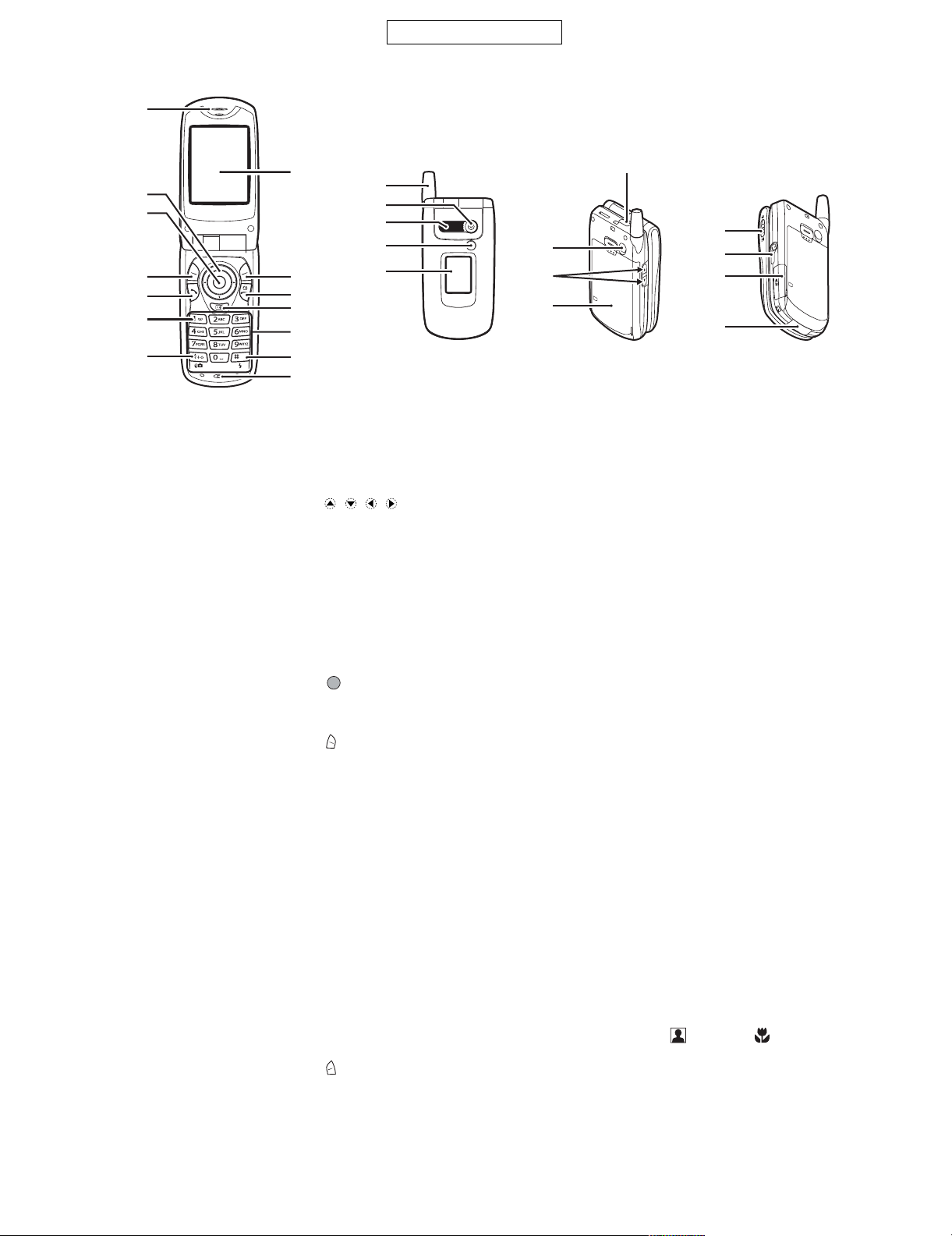
[2] Names of parts
1
CONFIDENTIAL
8
2
3
4
5
6
9
10
11
15
16
17
18
19
21
22
23
12
7
13
20
24
25
26
27
14
1. Earpiece
2. Navigation Keys (Arrow Keys):
Moves cursor to select
menu items, etc.
,,, inthis
manual indicate these keys.
Up/Down arrow keys: Displays Contacts List
entries in stand-by mode.
Left arrow key: Displays list of
Applications in stand-by
mode.
Right arrow key: Displays Pictures screen in
stand-by mode.
3. Centre Key: Displays Main menu in
stand-by mode and
executes functions.
in this manual indicates
this key.
4. Left Soft Key: Executes the functionat the
bottom left of the screen.
in this manual indicates
this key.
5. Send Key: Makes or accepts calls,
views the call in stand-by
mode.
6. Voice Mail Key: Press and hold this key to
connect to the Voice mail
centre automatically.
(Depends on the SIM card.)
7. * /Shift Key,
Viewfinder Switch Key:
Switches character case
among four modes: Abc,
ABC, 123 and abc.
Switches viewfinders
between main display and
external display in digital
camera/video camera
mode.
8. Main Display
9. Right Soft Key: Executesthe functionat the
bottom right of the screen.
in this manual indicates
this key.
Used to access “Vodafone
live!” by opening the
browser in stand-by mode.
10.End/Power Key: Ends a call, turns power on/
off.
11.Camera Key: Starts the digital camera in
stand-by mode.
12.Keypad
13.#/Flash light Key: Switches symbol screens.
Press and hold this key to
shift text input method
between multi-tap and T9
mode.
Turns the flash/auxiliary
light on or off in digital
camera/video camera
mode.
14.Microphone
15.Aerial
16.Camera
17.Speaker
18.Mobile Light:Usedasaflashoran
auxiliary light in digital
camera/video camera
mode, as a battery charge
indicator, or notification for
incoming calls, data/fax
calls or messages.
19.External Display
20.Infrared Port:Sendsandreceivesdatavia
infrared.
21.RF Connector
22.Side-Up/Side-Down Keys:
Moves cursor to select
menu items, adjusts
earpiece volume, etc.
In stand-by mode, press
and hold this key to turn the
mobile light on and off.
When the mobile light is
on,pressthiskeytochange
the light colour.
23.Battery Cover
24.Macro Switch: Switches between normal
(Close-up) ()andmacro()
position.
25.Handsfree Kit Connector
26.Memory Card Slot Cover
27.External Connector:
Used to connect either the
charger or USB data cable.
1 – 2
Page 5

[3] Operation manual
(Page numbers refer to the user guide)
[Optional Accessories]
Spare Lithium-ion battery (XN-1BT30)
High capacity Lithium-ion battery (XN-1BT31)
Cigarette lighter charger (XN-1CL30)
USB data cable (USB cable: XN-1DC30)
AC charger (XN-1QC30, XN-1QC31, XN-1QC32)
Personal handsfree kit (XN-1ER20)
The above accessories may not be available in all regions.
For details, please contact your dealer.
CONFIDENTIAL
GX30
[Quickstart Guide]
1 – 3
Page 6

GX30
CONFIDENTIAL
New Messages
Download Games
News Sport
12
1 – 4
Page 7
CONFIDENTIAL
GX30
6-3-3
1-3
7-5
1 – 5
Page 8

GX30
– MEMO –
CONFIDENTIAL
1 – 6
Page 9

CONFIDENTIAL
PhoneGX30Service ManualService ManualMarketE
CHAPTER 2. ADJUSTMENTS, PERFORMANCE CHECK, AND FIRMWARE
GX30
UPGRADE
SPST (SHARP Program Support Tool) allows you to adjust settings, conduct performance checks, and upgrade the firmware.
[1] SHARP Program Support Tool (SPST)
1. System requirements
• IBM PC compatible personal computer (standard COM1 115,200 bps serial port and USB required)
Supported OS: Windows 98/98SE/2000/XP (except for Windows 95/ME/NT)
(English, German, Italian, Spanish, French and Chinese versions)
• Data cable
<During RF adjustment>
• GSM tester: CMU200
• GPIB interface: National Instruments USB-GPIB cable (Model No.: NI GPIB-USB-B)
2. Introduction
2.1. Functions
SPST offers seven key functions:
1) Firmware download
2) User data transfer (processes all data at once but not individually.)
3) RF calibration check and test
4) Default setting
5) Identification
6) Performance check and adjustment
7) User password reset
2.2. Installation
1. Use Windows Explorer to execute the “setup.exe” file on the CD-ROM.
2. The SPST GX30 setup wizard appears. Follow the installation instructions.
3. After the installation is complete, shortcuts to SPST are created on the desktop and under the “Start” — “Programs” — “GX30” menu. Start SPST
from the shortcuts.
2 – 1
Page 10

GX30
CONFIDENTIAL
2.3. Starting up
Connect GX30 to an operable serial port of the PC with the supplied data cable. Make sure that the battery is fully charged.
Start SPST from the desktop.
1. The Input password dialog box appears. Enter the password, select a port where GX30 is connected from the list box, and click “OK”.
If you do not know SPC, click “Cancel” to exit.
Figure 1
2. To change the password, enter the current password in figure 1, and then click “Change Password”.
Figure 2
3. To check the usage status of tools, click “Show Repair Log” in figure 1.
4. Click “Downloader for Emergency”.
Figure 3
The above screen appears. Select a model to use and execute the Downloader. (Use this to initialize the flash, etc.)
2 – 2
Page 11

CONFIDENTIAL
5. When the password is correct, a connection is established and the following screen appears.
Refer to the attachment 1
for the destination and
operator name.
Figure 4
Buttons
GX30
Software version:
A02-006-0184-GX30
Default Set Refer to “4.1. Default setting”. (see page 2-5)
User Data Back-up Refer to “4.2. User data back-up”. (see page 2-6)
User Data Restore Refer to “4.3. User data restore”. (see page 2-7)
Downloader Refer to “4.4. Downloader”. (see page 2-8)
RF Calibration & Check Refer to “4.5. RF calibration & check”. (see page 2-19)
RF Test Refer to “4.6. RF test tool”. (see page 2-28)
User Password Reset Refer to “4.7. Password reset”. (see page 2-34)
Performance check adjustment Refer to “4.8. Performance check and adjustment”. (see page 2-35)
**** mode release Refer to “4.9. ****mode release”. (see page 2-42)
Exit End SPST.
Attachment 1 Destination and Operator name Chart
No. Operator name Country Model name
01 Vodafone UK Post-Paid UK A4TQGX30E
02 Airtel Post-Paid Spain A4TQGX30S
03 SFR Post-Paid France A4TQGX30F
04 Vodafone Omnitel Post-Paid Italy A4TQGX30T
05 D2 Post-Paid Germany A4TQGX30G
06 Vodafone NL Post-Paid Netherlands (Holland) A4TQGX30H
08 Vodafone Ireland Post-Paid Ireland A4TQGX30R
10 Vodafone Greece Post-Paid Greece A4TQGX30D
11 Vodafone Hungary Post-Paid Hungary A4TQGX30B
12 Vodafone Australia Post-Paid Australia A4TQGX30A
13 Vodafone New Zealand Post-Paid New Zealand A4TQGX30Z
14 Vodafone Sweden Post-Paid Sweden A4TQGX30W
15 Vodafone Egypt Post-Paid Egypt A4TQGX30Q
16 Vodafone Malta Post-Paid Malta A4TQGX30L
17 Swisscom Post-Paid Switzerland A4TQGX30C
18 mobilkom austria Post-Paid Austria A4TQGX30K
19 Belgacom mobile Post-Paid Belgium A4TQGX30U
48 Vodafone PT Pre-Paid Portugal A4TQGX30PP
50 Vodafone UK Pre-Paid UK A4TQGX30EP
2 – 3
Page 12

GX30
CONFIDENTIAL
3. Adjustments for GX30
1. Adjustments are required after replacing the following parts. ( )
Parts Temperature
adjustment
(Camera)
TH101
TH701
Main display unit
External display unit
Camera unit
When replacing other parts in the RF section, carry out RF calibration.
2. Click the buttons on the SPST screen for adjustments.
Temperature
adjustment
(Battery)
Main display
flicker
adjustment
External dis-
play contrast
adjustment
White defect
correction
RF calibration
Black defect
correction
3. The following screen appears.
To adjust the device, click this button
(Performance check adjustment).
Figure 5
Temperature adjustment (Camera section)
Temperature adjustment (Battery section)
Main display flicker adjustment
External display contrast adjustment
White defect correction
Black defect correction
Figure 6
2 – 4
Page 13

CONFIDENTIAL
4. Functions
4.1. Default setting
SPST can restore the factory settings.
This function
1. Deletes all user data in the file system;
2. Restores all WAP settings to default; and
3. Restores the values set by the user to default;
(MEP_LOCK settings and the destination and operator name do not change.)
<Operation>
1) Set the COM port on the SPST initial screen and click “Default Set”.
2) Click “Yes” to proceed. Click “No” to exit.
GX30
Figure 7
3) Click “Yes” to back-up the MEPLOCK data. Click “No” to restore default settings.
Figure 8
4) Communication starts.
Figure 9
5) The following appears when you select “Yes” in step 3 and MEPLOCK data exists. Click “Yes” to restore the data.
Figure 10
2 – 5
Page 14

GX30
6) After the handset is turned on, the initialization is complete.
CONFIDENTIAL
Figure 11
4.2. User data back-up
SPST saves all the data stored on the handset.
1. Set the COM port on the SPST initial screen and click “User Data Back-up”.
2. Specify the file name in the following dialog box and click “Save”.
3. The communicating dialog box appears while processing.
4. When completed, the following message appears. Click “OK”.
Figure 12
Figure 13
Figure 14
2 – 6
Page 15

CONFIDENTIAL
4.3. User data restore
SPST completely restores the backed up data.
1. Set the COM port on the SPST initial screen and click “User Data Restore”.
2. Specify the file name in the following dialog box and click “Save”.
GX30
3. The communicating dialog box appears while processing.
4. When the restore is complete, click “OK”.
Figure 15
Figure 16
Figure 17
2 – 7
Page 16

GX30
CONFIDENTIAL
4.4. Downloader
4.4.1 Introduction
Downloader allows you to upgrade the firmware.
1) Required devices
The following devices are required to rewrite MOT files using Communication Box.
Conversion connector (16-pin → 10-pin)
This conversion connector is required to connect GX30 with Communication Box since the cable connector of Communication Box has 16 pins.
Figure 18
2) Connecting handset to a PC
A) Using a cable for upgrading
1. Connect the cable to a PC.
2. Connect the cable to handset.
3. The photo below shows handset connected to a PC.
Figure 19
B) Using Communication Box
1. Connect a PC to Communication Box via a serial cable.
2. Connect the AC charger to Communication Box and then plug it into the outlet.
All SET POWER SW on Communication Box must be turned off.
3. Connect the conversion connector to Communication Box Cables.
Connect the conversion connector in the following order, label side up.
From upper right end: Cable No. 1, 3, 5, 7, and 9.
From lower right end: Cable No. 2, 4, 6, 8, and 10.
Figure 20
2 – 8
Page 17

CONFIDENTIAL
4. The photo below shows the conversion connector connected to Communication Box Cable 1.
Figure 21
5. Connect the other end of the conversion connector to handset.
GX30
Figure 22
6. The photo below shows handset, Communication Box and a PC (all connected).
Make sure handset and Communication Box Cable 1 are connected via the conversion connector.
Figure 23
[Note]
Handset must be turned off before making any connections.
Press and hold the Power key to turn off handset.
Do not turn off in other ways. Malfunction may occur and the MOT file rewrite operation may fail.
Make sure the handset battery is sufficiently charged.
If the battery is low, the MOT file rewrite operation may fail.
Charge the battery before the operation.
Disconnect the AC charger from a cable for upgrading.
When rewriting MOT files using the upgrading tool, do not connect the AC charger to the cable.
If you connect the cable connected to the AC charger to handset, charging starts and the MOT file rewrite operation is interrupted.
All SET POWER SW on Communication Box must be turned off.
If handset is connected with SET POWER SW turned on, charging starts and the MOT file rewrite operation is interrupted.
Make sure handset and Communication Box Cable 1 are connected via the conversion connector.
(When using Communication Box, the only handset connected to Cable 1 can be operated on the PC.)
2 – 9
Page 18

GX30
CONFIDENTIAL
4.4.2 Rewriting MOT files
This section describes how to rewrite MOT files using the upgrading tool.
1) Activating Software
1. Double click the shortcut icon on your desktop or click “The GX30 Upgrading Tool” on the Start menu.
Figure 24
2. The upgrading tool is activated.
Figure 25
[Note]
Disable the power saving mode before rewriting MOT files.
If the power saving mode is active, the rewrite operation may fail depending on the PC.
2 – 10
Page 19

CONFIDENTIAL
GX30
2) Selecting options and COM port
1. Uncheck the check box when using a cable for upgrading. Leave it checked when using Communication Box.
2. To initialize user area, check the File System Initialize check box. (User data will be deleted and the handset status will return to the default.)
3. Click here and in the pull-down list, select a communications port where the cable or Communication Box is connected.
1
3
2
Figure 26
When using Communication Box, set Wait Time.
Check the Communication Box check box to adjust Wait Time (default: 8 seconds). The time to delete the program data varies between handsets.
Handsets wait for the set Wait Time until the whole process is completed. If an error occurs, increase the value.
Figure 27
[Notes for the Wait Time setting]
When the set value is smaller than the default (8), the message on the left appears alerting you a possible error.
Click the “OK” button to proceed, and click the “Cancel” button to change the value.
Figure 28
2 – 11
Page 20

GX30
You can shorten time for the MOT file rewrite operation by selecting a smaller value for Wait Time.
Example: Time to rewrite two MOT files at a time.
At the default setting (8 seconds), rewrite time is approximately one hour.
If the value is set to 1, the rewrite time will be reduced to approximately 30 minutes.
If an error occurs at 1, increase the value.
The error screen will appear on handsets No. 2 to No.10.
If this screen appears, increase Wait Time and retry.
CONFIDENTIAL
Error screen
Flash Loader 5.02
CORRESPONDENCE_ERROR
Figure 29
When the File System Initialize check box is checked, a confirmation message appears.
Click the [OK] button.
Figure 30
[Note]
When you check File System Initialize check box and click the “OK” button, handset status returns to the default.
In this case, user data is initialized after the MOT file rewrite operation. Uncheck the check box to avoid this.
2 – 12
Page 21

CONFIDENTIAL
3) Selecting a MOT file
1. Click the “Select File” button.
The Open dialog box appears.
[Open dialog box]
2. Click the “ ” button to open a desired folder.
3. A Motorola file (.mot) in the folder appears. Click a file to write in.
4. Click the “Open” button to open the file.
GX30
Figure 31
2
3
4
Figure 32
[Note]
Make sure to select a MOT file.
If the File name field is blank, you cannot rewrite a MOT file.
Use MOT files in the hard disk.
If the selected MOT file is stored in other locations, an error message appears and you cannot complete the rewrite operation.
Figure 33
To use MOT files on CDs or on the network, copy or download them to the hard disk first.
2 – 13
Page 22

GX30
CONFIDENTIAL
4) Rewriting a MOT file
Click the “Start Loading Flash” button to start rewriting.
Figure 34
1. “Press Power Button” appears.
<When using a cable for upgrading>
Hold down the Power key.
<When using the Communication Box>
Turn on handsets from No.10 down to No.1 (turn on only the handsets you are using).
Figure 35
2. “Keep Pressing Power Button” appears.
<When using a cable for upgrading>
Hold down the Power key until the “Keep Pressing Power Button” disappears.
<When using the Communication Box>
Leave the handsets turned on.
Figure 36
2 – 14
Page 23

CONFIDENTIAL
3. The MOT file rewrite operation starts.
<When using a cable for upgrading>
When “Keep Pressing Power Button” disappears, release the Power key.
<When using the Communication Box>
Leave the handsets turned on.
Figure 37
4. When the rewrite operation starts, handset display screen shows the software version and process of communications with the PC.
Flash Loader 5.02
GX30
XXXXXXXCommand
Figure 38
Canceling the ongoing rewrite operation:
Click the “QUIT” button.
To rewrite MOT files later, remove and install the battery first.
[Notes for the use of a cable for upgrading]
1. Disconnect the AC charger from the cable. Otherwise charging starts and the MOT file rewrite operation is interrupted.
2. Make sure the handset battery is sufficiently charged.
If the battery is low, the rewrite operation may fail. Charge the battery before the operation.
3. If the ongoing rewrite operation is canceled, or interrupted by an error, remove and reinstall the battery and retry.
[Notes for the use of the Communication Box]
1. When “Press Power Button!” appears, turn on handsets from No.10 down to No.1. If the handset No.1 is first turned on, the rewrite on handsets
No. 2 to No. 10 operation will fail.
2. The time to delete the program data varies between handsets. If the process fails at the default Wait Time (8 seconds), increase the value.
Consequently, this will increase the time to complete the rewrite operation.
2 – 15
Page 24

GX30
CONFIDENTIAL
5) Checking the value of SUM
When the rewrite operation is completed, a confirmation message appears with SUM.
Figure 39
SUM also appears on handset.
<When using a cable for upgrading>
After 8 seconds, SUM disappears.
<When using Communication Box>
When SET POWER SW is turned off, SUM disappears.
Flash Loader 5.02
SUM Check End
SUM = 0xdb3d
Figure 40
Make sure SUM is the same between the PC and handset.
The same SUM means that the rewrite operation is completed properly. If the value is different, try again to ensure completion of the operation.
If the MOT file rewrite operation fails, an error message appears on handset.
* The screen shot on the left shows an error in erasing Flash data.
“ADR” and “STR” appear only when an error occurs in the FLASH-related operation.
Start over the MOT file rewrite operation.
<When other error messages appear>
Find the message in [4.4.3.2) Error messages for Loading loader (see page 2-18)], and follow the instructions.
Error screen
Flash Loader 5.02
FLASH_ERROR
ERROR_ERASE
ADR = 0x1000000
STR = 0xA0
Figure 41
2 – 16
Page 25

CONFIDENTIAL
6) After the operation
Disconnect the cable for upgrading from handset.
When using the Communication Box, turn off SET POWER SW and then disconnect the cable from handset.
7) Initializing only the file system
Follow the instructions below to initialize only the file system.
(User data will be deleted and the handset status will return to the default.)
* Perform this procedure when the handset does not turn on.
1. Check the File System Initialize check box.
2. Leave the Load File text box blank.
3. Click the “Start Loading Flash” button.
1
GX30
2
3
Figure 42
For further operations, refer to [4.4.2.4) Rewriting a MOT file (see page 2-14)] or [4.4.2.5) Checking the value of SUM (see page 2-16)].
2 – 17
Page 26

GX30
CONFIDENTIAL
4.4.3 Error message list
Below is the list of error messages for the upgrading tool (on the PC side) and Loading loader (on the handset side).
1) Error messages for the upgrading tool (on the PC side)
No. Message Descriptions/Instructions
1 Select a file for Downloading or check the box of Initializing. Load File is not set.
Select a MOT file.
2 Unable to open file. Failed to open the MOT file.
Start over the rewrite operation.
3 You need to set the Wait Time! WaitTime (S) is not set.
Set WaitTime (S) value.
4 The file you selected is unsuitable for Upgrading. The selected file cannot be rewritten for upgrading.
Select an appropriate MOT file.
5 Cannot Setup COM port. The selected COM port does not exist or is used for other opera-
tions.
Select a COM port connected to the PC cable.
6 RAM Loader not responding to Commands. No response from Loading loader.
7 RAM Loader responding Parameter Error. Information sent from the PC is illegal.
8 RAM Loader responding Flash Error (XXXX). Failed to initialize FLASH ROM in (XXXX).
9 Correspondence Error. Undefined response from Loading loader.
Start over the rewrite operation.
Reinstall the upgrading tool.
Start over the rewrite operation.
Start over the rewrite operation.
Start over the rewrite operation.
2) Error messages for Loading loader (on the handset side)
No. Message Descriptions/Instructions
1 FLASH_ERROR An error in Flash Rom.
2 ERROR_PARAM The upgrading tool is damaged.
3 ERROR_WPROTECT Flash Rom is protected.
4 ERROR_READ Failed to read Flash Rom data and the operation was aborted.
5 ERROR_WRITE Failed to write to Flash Rom and the operation was aborted.
6 ERROR_ERASE Failed to erase Flash Rom data and the operation was aborted.
7 ERROR_VERIFY The rewrite operation was aborted since there was a mismatch
8 ERROR_RWE_TMOUT Communication was terminated since there was no response from
9 CORRESPONDENCE_ERROR Communication was terminated since serial data communication
10 ADR = XXXXXXXX Indicates the address of Flash (the error source).
11 STR =XX Indicates the status of Flash (the error source).
* When No.1 occurs, handset screen shows error messages for No.2 to No.8 as well as the address (No.10) and status (No.11) of the error source
at the same time.
Start over the rewrite operation.
Uninstall and reinstall the upgrading tool, and start over the rewrite
operation.
Battery may be too low.
Use a sufficiently charged battery and start over the rewrite operation.
Start over the rewrite operation.
Start over the rewrite operation.
Start over the rewrite operation.
between data written to Flash Rom and that written to handset.
Start over the rewrite operation.
Flash Rom for a certain period of time.
Start over the rewrite operation.
failed.
Start over the rewrite operation.
2 – 18
Page 27

4.5. RF calibration & check
CONFIDENTIAL
GX30
Stabilized power supply
Test battery
Handset
Data cable
RF cable
GSM tester
GPIB cable
PC
Figure 43
4.5.1 Preparation
• Connect PC and GSM tester with a GPIB cable.
• Connect PC and handset with a Data cable. (Use a test battery or one close.)
• Connect a RF cable of GSM tester to handset.
2 – 19
Page 28

GX30
4.5.2 Default setting for the program.
• Activate the program and set defaults.
CONFIDENTIAL
1) Select the COM port.
2) Set the GPIB No.
3) Select the test instrument.
4) Set the GPIB address.
Figure 44
5) Set the "Cable Offset" values.
For cables with connector
QCNWK0138AFZZ/
QCNWK0136AFZZ, set the
values as follows:
GSM 900: 0.60
DCS 1800: 0.95
PCS 1900: 0.96
GSM 850: 0.60
6) Auto Dial Setting
When the Auto Dial check
box is checked, an entered
number is automatically
dialed for performance
check.
7) Number Setting
Enter a number for Auto Dial.
2 – 20
Page 29

CONFIDENTIAL
GX30
4.5.3 RF calibration
1. Apply 4 V using a stabilized power supply and turn on the handset.
2. Start “RF calibration & check” on SPST and click “Calibration”.
3. When initialization is complete, click “OK”.
Figure 45
4. Apply 4 V using a stabilized power supply and turn on the handset. After the handset enters Standby mode, lower the voltage to 3.7 V, click “OK”.
Figure 46
5. Make sure the handset is on and click “OK”.
(Adjustment starts.)
Figure 47
6. Click “OK”.
Figure 48
7. The initial screen returns.
<Note>
The following appears when the handset software (mot) is outdated. Upgrade to a new version.
Figure 49
2 – 21
Page 30

GX30
CONFIDENTIAL
4.5.4 RF performance check
1. Apply 4 V using a stabilized power supply and turn on the handset.
2. Start “RF calibration & check” on SPST and click “Check”.
3. When initialization is complete, click “OK”.
Figure 50
4. Apply 4 V using a stabilized power supply and turn on the handset. After the handset enters Standby mode, lower the voltage to 3.7 V, enter the
PIN code and click “OK”.
Figure 51
5. Make sure the handset is in the idle mode and click “OK”.
Figure 52
6. RF performance check is complete. Click “Save As...” and name the file to save the result. Click “OK” to exit.
Figure 53
2 – 22
Page 31

The following will be displayed in case of failure.
See the attachment 2 for troubleshooting.
CONFIDENTIAL
GX30
7. Click “OK”.
8. The initial screen returns.
Figure 54
Figure 55
2 – 23
Page 32

GX30
Attachment 2
Whole inspection list by RF performance check.
Band Send-
Recei
GSM Tx 1 Burst Power 37CH PCL5
900 2 Burst Power 975CH PCL5
No. Item to be inspected Chan-
ing/
ve
3 Burst Power 124CH PCL5
4 Burst Power 37CH PCL11
5 Burst Power 37CH PCL19
6 Frequency Error 37CH PCL5
7 Frequency Error 975CH PCL5
8 Frequency Error 124CH PCL5
9 Phase Error (RMS) 37CH PCL5
10 Phase Error (RMS) 975CH PCL5
11 Phase Error (RMS) 124CH PCL5
12 Phase Error (Peak) 37CH PCL5
13 Phase Error (Peak) 975CH PCL5
14 Phase Error (Peak) 124CH PCL5
15 Mod_spectrum –800 37CH PCL5
16 Mod_spectrum –600 37CH PCL5
17 Mod_spectrum –400 37CH PCL5
18 Mod_spectrum –250 37CH PCL5
19 Mod_spectrum –200 37CH PCL5
20 Mod_spectrum +200 37CH PCL5
21 Mod_spectrum +250 37CH PCL5
22 Mod_spectrum +400 37CH PCL5
23 Mod_spectrum +600 37CH PCL5
24 Mod_spectrum +800 37CH PCL5
25 Mod_spectrum –800 975CH PCL5
26 Mod_spectrum –600 975CH PCL5
27 Mod_spectrum –400 975CH PCL5
28 Mod_spectrum –250 975CH PCL5
29 Mod_spectrum –200 975CH PCL5
30 Mod_spectrum +200 975CH PCL5
31 Mod_spectrum +250 975CH PCL5
32 Mod_spectrum +400 975CH PCL5
33 Mod_spectrum +600 975CH PCL5
34 Mod_spectrum +800 975CH PCL5
35 Mod_spectrum –800 124CH PCL5
36 Mod_spectrum –600 124CH PCL5
37 Mod_spectrum –400 124CH PCL5
38 Mod_spectrum –250 124CH PCL5
39 Mod_spectrum –200 124CH PCL5
40 Mod_spectrum +200 124CH PCL5
41 Mod_spectrum +250 124CH PCL5
42 Mod_spectrum +400 124CH PCL5
43 Mod_spectrum +600 124CH PCL5
44 Mod_spectrum +800 124CH PCL5
45 Mod_spectrum –800 37CH PCL11
46 Mod_spectrum –600 37CH PCL11
47 Mod_spectrum –400 37CH PCL11
48 Mod_spectrum –250 37CH PCL11
49 Mod_spectrum –200 37CH PCL11
50 Mod_spectrum +200 37CH PCL11
51 Mod_spectrum +250 37CH PCL11
52 Mod_spectrum +400 37CH PCL11
53 Mod_spectrum +600 37CH PCL11
54 Mod_spectrum +800 37CH PCL11
55 Mod_spectrum –800 37CH PCL19
56 Mod_spectrum –600 37CH PCL19
57 Mod_spectrum –400 37CH PCL19
58 Mod_spectrum –250 37CH PCL19
59 Mod_spectrum –200 37CH PCL19
60 Mod_spectrum +200 37CH PCL19
CONFIDENTIAL
nel
PCL
Band Send-
Recei
Rx 110 Rx Sensitivity 37CH PCL5
DCS Tx 115 Burst Power 699CH PCL0
No. Item to be inspected Chan-
ing/
ve
61 Mod_spectrum +250 37CH PCL19
62 Mod_spectrum +400 37CH PCL19
63 Mod_spectrum +600 37CH PCL19
64 Mod_spectrum +800 37CH PCL19
65 Switch_Spectrum –1800 37CH PCL5
66 Switch_Spectrum –1200 37CH PCL5
67 Switch_Spectrum –600 37CH PCL5
68 Switch_Spectrum –400 37CH PCL5
69 Switch_Spectrum +400 37CH PCL5
70 Switch_Spectrum +600 37CH PCL5
71 Switch_Spectrum +1200 37CH PCL5
72 Switch_Spectrum +1800 37CH PCL5
73 Switch_Spectrum –1800 975CH PCL5
74 Switch_Spectrum –1200 975CH PCL5
75 Switch_Spectrum –600 975CH PCL5
76 Switch_Spectrum –400 975CH PCL5
77 Switch_Spectrum +400 975CH PCL5
78 Switch_Spectrum +600 975CH PCL5
79 Switch_Spectrum +1200 975CH PCL5
80 Switch_Spectrum +1800 975CH PCL5
81 Switch_Spectrum –1800 124CH PCL5
82 Switch_Spectrum –1200 124CH PCL5
83 Switch_Spectrum –600 124CH PCL5
84 Switch_Spectrum –400 124CH PCL5
85 Switch_Spectrum +400 124CH PCL5
86 Switch_Spectrum +600 124CH PCL5
87 Switch_Spectrum +1200 124CH PCL5
88 Switch_Spectrum +1800 124CH PCL5
89 Switch_Spectrum –1800 37CH PCL11
90 Switch_Spectrum –1200 37CH PCL11
91 Switch_Spectrum –600 37CH PCL11
92 Switch_Spectrum –400 37CH PCL11
93 Switch_Spectrum +400 37CH PCL11
94 Switch_Spectrum +600 37CH PCL11
95 Switch_Spectrum +1200 37CH PCL11
96 Switch_Spectrum +1800 37CH PCL11
97 Switch_Spectrum –1800 37CH PCL19
98 Switch_Spectrum –1200 37CH PCL19
99 Switch_Spectrum –600 37CH PCL19
100 Switch_Spectrum –400 37CH PCL19
101 Switch_Spectrum +400 37CH PCL19
102 Switch_Spectrum +600 37CH PCL19
103 Switch_Spectrum +1200 37CH PCL19
104 Switch_Spectrum +1800 37CH PCL19
105 Burst Timing 37CH PCL5
106 Burst Timing 975CH PCL5
107 Burst Timing 124CH PCL5
108 Burst Timing 37CH PCL11
109 Burst Timing 37CH PCL19
111 Rx Sensitivity 975CH PCL5
112 Rx Sensitivity 124CH PCL5
113 Usable Receiver Level 37CH PCL5
114 Rx Level Reports 37CH PCL5
116 Burst Power 512CH PCL0
117 Burst Power 885CH PCL0
118 Burst Power 699CH PCL5
119 Burst Power 699CH PCL15
120 Frequency Error 699CH PCL0
121 Frequency Error 512CH PCL0
122 Frequency Error 885CH PCL0
nel
PCL
2 – 24
Page 33

Band Send-
ing/
Recei
ve
CONFIDENTIAL
No. Item to be inspected Chan-
nel
123 Phase Error (RMS) 699CH PCL0
124 Phase Error (RMS) 512CH PCL0
125 Phase Error (RMS) 885CH PCL0
126 Phase Error (Peak) 699CH PCL0
127 Phase Error (Peak) 512CH PCL0
128 Phase Error (Peak) 885CH PCL0
129 Mod_spectrum –800 699CH PCL0
130 Mod_spectrum –600 699CH PCL0
131 Mod_spectrum –400 699CH PCL0
132 Mod_spectrum –250 699CH PCL0
133 Mod_spectrum –200 699CH PCL0
134 Mod_spectrum +200 699CH PCL0
135 Mod_spectrum +250 699CH PCL0
136 Mod_spectrum +400 699CH PCL0
137 Mod_spectrum +600 699CH PCL0
138 Mod_spectrum +800 699CH PCL0
139 Mod_spectrum –800 512CH PCL0
140 Mod_spectrum –600 512CH PCL0
141 Mod_spectrum –400 512CH PCL0
142 Mod_spectrum –250 512CH PCL0
143 Mod_spectrum –200 512CH PCL0
144 Mod_spectrum +200 512CH PCL0
145 Mod_spectrum +250 512CH PCL0
146 Mod_spectrum +400 512CH PCL0
147 Mod_spectrum +600 512CH PCL0
148 Mod_spectrum +800 512CH PCL0
149 Mod_spectrum –800 885CH PCL0
150 Mod_spectrum –600 885CH PCL0
151 Mod_spectrum –400 885CH PCL0
152 Mod_spectrum –250 885CH PCL0
153 Mod_spectrum –200 885CH PCL0
154 Mod_spectrum +200 885CH PCL0
155 Mod_spectrum +250 885CH PCL0
156 Mod_spectrum +400 885CH PCL0
157 Mod_spectrum +600 885CH PCL0
158 Mod_spectrum +800 885CH PCL0
159 Mod_spectrum –800 699CH PCL5
160 Mod_spectrum –600 699CH PCL5
161 Mod_spectrum –400 699CH PCL5
162 Mod_spectrum –250 699CH PCL5
163 Mod_spectrum –200 699CH PCL5
164 Mod_spectrum +200 699CH PCL5
165 Mod_spectrum +250 699CH PCL5
166 Mod_spectrum +400 699CH PCL5
167 Mod_spectrum +600 699CH PCL5
168 Mod_spectrum +800 699CH PCL5
169 Mod_spectrum –800 699CH PCL15
170 Mod_spectrum –600 699CH PCL15
171 Mod_spectrum –400 699CH PCL15
172 Mod_spectrum –250 699CH PCL15
173 Mod_spectrum –200 699CH PCL15
174 Mod_spectrum +200 699CH PCL15
175 Mod_spectrum +250 699CH PCL15
176 Mod_spectrum +400 699CH PCL15
177 Mod_spectrum +600 699CH PCL15
178 Mod_spectrum +800 699CH PCL15
179 Switch_Spectrum –1800 699CH PCL0
180 Switch_Spectrum –1200 699CH PCL0
181 Switch_Spectrum –600 699CH PCL0
182 Switch_Spectrum –400 699CH PCL0
183 Switch_Spectrum +400 699CH PCL0
184 Switch_Spectrum +600 699CH PCL0
PCL
GX30
Band Send-
Recei
Rx 224 Rx Sensitivity 699CH PCL0
PCS Tx 229 Burst Power 661CH PCL0
No. Item to be inspected Chan-
ing/
ve
185 Switch_Spectrum +1200 699CH PCL0
186 Switch_Spectrum +1800 699CH PCL0
187 Switch_Spectrum –1800 512CH PCL0
188 Switch_Spectrum –1200 512CH PCL0
189 Switch_Spectrum –600 512CH PCL0
190 Switch_Spectrum –400 512CH PCL0
191 Switch_Spectrum +400 512CH PCL0
192 Switch_Spectrum +600 512CH PCL0
193 Switch_Spectrum +1200 512CH PCL0
194 Switch_Spectrum +1800 512CH PCL0
195 Switch_Spectrum –1800 885CH PCL0
196 Switch_Spectrum –1200 885CH PCL0
197 Switch_Spectrum –600 885CH PCL0
198 Switch_Spectrum –400 885CH PCL0
199 Switch_Spectrum +400 885CH PCL0
200 Switch_Spectrum +600 885CH PCL0
201 Switch_Spectrum +1200 885CH PCL0
202 Switch_Spectrum +1800 885CH PCL0
203 Switch_Spectrum –1800 699CH PCL5
204 Switch_Spectrum –1200 699CH PCL5
205 Switch_Spectrum –600 699CH PCL5
206 Switch_Spectrum –400 699CH PCL5
207 Switch_Spectrum +400 699CH PCL5
208 Switch_Spectrum +600 699CH PCL5
209 Switch_Spectrum +1200 699CH PCL5
210 Switch_Spectrum +1800 699CH PCL5
211 Switch_Spectrum –1800 699CH PCL15
212 Switch_Spectrum –1200 699CH PCL15
213 Switch_Spectrum –600 699CH PCL15
214 Switch_Spectrum –400 699CH PCL15
215 Switch_Spectrum +400 699CH PCL15
216 Switch_Spectrum +600 699CH PCL15
217 Switch_Spectrum +1200 699CH PCL15
218 Switch_Spectrum +1800 699CH PCL15
219 Burst Timing 699CH PCL0
220 Burst Timing 512CH PCL0
221 Burst Timing 885CH PCL0
222 Burst Timing 699CH PCL5
223 Burst Timing 699CH PCL15
225 Rx Sensitivity 512CH PCL0
226 Rx Sensitivity 885CH PCL0
227 Usable Receiver Level 699CH PCL0
228 Rx Level Reports 699CH PCL0
230 Burst Power 512CH PCL0
231 Burst Power 810CH PCL0
232 Burst Power 661CH PCL5
233 Burst Power 661CH PCL15
234 Frequency Error 661CH PCL0
235 Frequency Error 512CH PCL0
236 Frequency Error 810CH PCL0
237 Phase Error (RMS) 661CH PCL0
238 Phase Error (RMS) 512CH PCL0
239 Phase Error (RMS) 810CH PCL0
240 Phase Error (Peak) 661CH PCL0
241 Phase Error (Peak) 512CH PCL0
242 Phase Error (Peak) 810CH PCL0
243 Mod_spectrum –800 661CH PCL0
244 Mod_spectrum –600 661CH PCL0
245 Mod_spectrum –400 661CH PCL0
246 Mod_spectrum –250 661CH PCL0
nel
PCL
2 – 25
Page 34

GX30
Band Send-
ing/
Recei
No. Item to be inspected Chan-
nel
ve
247 Mod_spectrum –200 661CH PCL0
248 Mod_spectrum +200 661CH PCL0
249 Mod_spectrum +250 661CH PCL0
250 Mod_spectrum +400 661CH PCL0
251 Mod_spectrum +600 661CH PCL0
252 Mod_spectrum +800 661CH PCL0
253 Mod_spectrum –800 512CH PCL0
254 Mod_spectrum –600 512CH PCL0
255 Mod_spectrum –400 512CH PCL0
256 Mod_spectrum –250 512CH PCL0
257 Mod_spectrum –200 512CH PCL0
258 Mod_spectrum +200 512CH PCL0
259 Mod_spectrum +250 512CH PCL0
260 Mod_spectrum +400 512CH PCL0
261 Mod_spectrum +600 512CH PCL0
262 Mod_spectrum +800 512CH PCL0
263 Mod_spectrum –800 810CH PCL0
264 Mod_spectrum –600 810CH PCL0
265 Mod_spectrum –400 810CH PCL0
266 Mod_spectrum –250 810CH PCL0
267 Mod_spectrum –200 810CH PCL0
268 Mod_spectrum +200 810CH PCL0
269 Mod_spectrum +250 810CH PCL0
270 Mod_spectrum +400 810CH PCL0
271 Mod_spectrum +600 810CH PCL0
272 Mod_spectrum +800 810CH PCL0
273 Mod_spectrum –800 661CH PCL5
274 Mod_spectrum –600 661CH PCL5
275 Mod_spectrum –400 661CH PCL5
276 Mod_spectrum –250 661CH PCL5
277 Mod_spectrum –200 661CH PCL5
278 Mod_spectrum +200 661CH PCL5
279 Mod_spectrum +250 661CH PCL5
280 Mod_spectrum +400 661CH PCL5
281 Mod_spectrum +600 661CH PCL5
282 Mod_spectrum +800 661CH PCL5
283 Mod_spectrum –800 661CH PCL15
284 Mod_spectrum –600 661CH PCL15
285 Mod_spectrum –400 661CH PCL15
286 Mod_spectrum –250 661CH PCL15
287 Mod_spectrum –200 661CH PCL15
288 Mod_spectrum +200 661CH PCL15
289 Mod_spectrum +250 661CH PCL15
290 Mod_spectrum +400 661CH PCL15
291 Mod_spectrum +600 661CH PCL15
292 Mod_spectrum +800 661CH PCL15
293 Switch_Spectrum –1800 661CH PCL0
294 Switch_Spectrum –1200 661CH PCL0
295 Switch_Spectrum –600 661CH PCL0
296 Switch_Spectrum –400 661CH PCL0
297 Switch_Spectrum +400 661CH PCL0
298 Switch_Spectrum +600 661CH PCL0
299 Switch_Spectrum +1200 661CH PCL0
300 Switch_Spectrum +1800 661CH PCL0
301 Switch_Spectrum –1800 512CH PCL0
302 Switch_Spectrum –1200 512CH PCL0
303 Switch_Spectrum –600 512CH PCL0
304 Switch_Spectrum –400 512CH PCL0
305 Switch_Spectrum +400 512CH PCL0
306 Switch_Spectrum +600 512CH PCL0
307 Switch_Spectrum +1200 512CH PCL0
308 Switch_Spectrum +1800 512CH PCL0
CONFIDENTIAL
PCL
Band Send-
GSM Tx 343 Burst Power 190CH PCL7
850 344 Burst Power 128CH PCL7
No. Item to be inspected Chan-
ing/
Recei
ve
309 Switch_Spectrum –1800 810CH PCL0
310 Switch_Spectrum –1200 810CH PCL0
311 Switch_Spectrum –600 810CH PCL0
312 Switch_Spectrum –400 810CH PCL0
313 Switch_Spectrum +400 810CH PCL0
314 Switch_Spectrum +600 810CH PCL0
315 Switch_Spectrum +1200 810CH PCL0
316 Switch_Spectrum +1800 810CH PCL0
317 Switch_Spectrum –1800 661CH PCL5
318 Switch_Spectrum –1200 661CH PCL5
319 Switch_Spectrum –600 661CH PCL5
320 Switch_Spectrum –400 661CH PCL5
321 Switch_Spectrum +400 661CH PCL5
322 Switch_Spectrum +600 661CH PCL5
323 Switch_Spectrum +1200 661CH PCL5
324 Switch_Spectrum +1800 661CH PCL5
325 Switch_Spectrum –1800 661CH PCL15
326 Switch_Spectrum –1200 661CH PCL15
327 Switch_Spectrum –600 661CH PCL15
328 Switch_Spectrum –400 661CH PCL15
329 Switch_Spectrum +400 661CH PCL15
330 Switch_Spectrum +600 661CH PCL15
331 Switch_Spectrum +1200 661CH PCL15
332 Switch_Spectrum +1800 661CH PCL15
333 Burst Timing 661CH PCL0
334 Burst Timing 512CH PCL0
335 Burst Timing 810CH PCL0
336 Burst Timing 661CH PCL5
337 Burst Timing 661CH PCL15
Rx 338 Rx Sensitivity 661CH PCL0
339 Rx Sensitivity 512CH PCL0
340 Rx Sensitivity 810CH PCL0
341 Usable Receiver Level 661CH PCL0
342 Rx Level Reports 661CH PCL0
345 Burst Power 251CH PCL7
346 Burst Power 190CH PCL11
347 Burst Power 190CH PCL19
348 Frequency Error 190CH PCL7
349 Frequency Error 128CH PCL7
350 Frequency Error 251CH PCL7
351 Phase Error (RMS) 190CH PCL7
352 Phase Error (RMS) 128CH PCL7
353 Phase Error (RMS) 251CH PCL7
354 Phase Error (Peak) 190CH PCL7
355 Phase Error (Peak) 128CH PCL7
356 Phase Error (Peak) 251CH PCL7
357 Mod_spectrum –800 190CH PCL7
358 Mod_spectrum –600 190CH PCL7
359 Mod_spectrum –400 190CH PCL7
360 Mod_spectrum –250 190CH PCL7
361 Mod_spectrum –200 190CH PCL7
362 Mod_spectrum +200 190CH PCL7
363 Mod_spectrum +250 190CH PCL7
364 Mod_spectrum +400 190CH PCL7
365 Mod_spectrum +600 190CH PCL7
366 Mod_spectrum +800 190CH PCL7
367 Mod_spectrum –800 128CH PCL7
368 Mod_spectrum –600 128CH PCL7
369 Mod_spectrum –400 128CH PCL7
370 Mod_spectrum –250 128CH PCL7
nel
PCL
2 – 26
Page 35

Band Send-
ing/
Recei
ve
CONFIDENTIAL
No. Item to be inspected Chan-
nel
371 Mod_spectrum –200 128CH PCL7
372 Mod_spectrum +200 128CH PCL7
373 Mod_spectrum +250 128CH PCL7
374 Mod_spectrum +400 128CH PCL7
375 Mod_spectrum +600 128CH PCL7
376 Mod_spectrum +800 128CH PCL7
377 Mod_spectrum –800 251CH PCL7
378 Mod_spectrum –600 251CH PCL7
379 Mod_spectrum –400 251CH PCL7
380 Mod_spectrum –250 251CH PCL7
381 Mod_spectrum –200 251CH PCL7
382 Mod_spectrum +200 251CH PCL7
383 Mod_spectrum +250 251CH PCL7
384 Mod_spectrum +400 251CH PCL7
385 Mod_spectrum +600 251CH PCL7
386 Mod_spectrum +800 251CH PCL7
387 Mod_spectrum –800 190CH PCL11
388 Mod_spectrum –600 190CH PCL11
389 Mod_spectrum –400 190CH PCL11
390 Mod_spectrum –250 190CH PCL11
391 Mod_spectrum –200 190CH PCL11
392 Mod_spectrum +200 190CH PCL11
393 Mod_spectrum +250 190CH PCL11
394 Mod_spectrum +400 190CH PCL11
395 Mod_spectrum +600 190CH PCL11
396 Mod_spectrum +800 190CH PCL11
397 Mod_spectrum –800 190CH PCL19
398 Mod_spectrum –600 190CH PCL19
399 Mod_spectrum –400 190CH PCL19
400 Mod_spectrum –250 190CH PCL19
401 Mod_spectrum –200 190CH PCL19
402 Mod_spectrum +200 190CH PCL19
403 Mod_spectrum +250 190CH PCL19
404 Mod_spectrum +400 190CH PCL19
405 Mod_spectrum +600 190CH PCL19
406 Mod_spectrum +800 190CH PCL19
407 Switch_Spectrum –1800 190CH PCL7
408 Switch_Spectrum –1200 190CH PCL7
409 Switch_Spectrum –600 190CH PCL7
410 Switch_Spectrum –400 190CH PCL7
411 Switch_Spectrum +400 190CH PCL7
412 Switch_Spectrum +600 190CH PCL7
413 Switch_Spectrum +1200 190CH PCL7
414 Switch_Spectrum +1800 190CH PCL7
415 Switch_Spectrum –1800 128CH PCL7
PCL
Band Send-
Recei
Rx 452 Rx Sensitivity 190CH PCL7
No. Item to be inspected Chan-
ing/
ve
416 Switch_Spectrum –1200 128CH PCL7
417 Switch_Spectrum –600 128CH PCL7
418 Switch_Spectrum –400 128CH PCL7
419 Switch_Spectrum +400 128CH PCL7
420 Switch_Spectrum +600 128CH PCL7
421 Switch_Spectrum +1200 128CH PCL7
422 Switch_Spectrum +1800 128CH PCL7
423 Switch_Spectrum –1800 251CH PCL7
424 Switch_Spectrum –1200 251CH PCL7
425 Switch_Spectrum –600 251CH PCL7
426 Switch_Spectrum –400 251CH PCL7
427 Switch_Spectrum +400 251CH PCL7
428 Switch_Spectrum +600 251CH PCL7
429 Switch_Spectrum +1200 251CH PCL7
430 Switch_Spectrum +1800 251CH PCL7
431 Switch_Spectrum –1800 190CH PCL11
432 Switch_Spectrum –1200 190CH PCL11
433 Switch_Spectrum –600 190CH PCL11
434 Switch_Spectrum –400 190CH PCL11
435 Switch_Spectrum +400 190CH PCL11
436 Switch_Spectrum +600 190CH PCL11
437 Switch_Spectrum +1200 190CH PCL11
438 Switch_Spectrum +1800 190CH PCL11
439 Switch_Spectrum –1800 190CH PCL19
440 Switch_Spectrum –1200 190CH PCL19
441 Switch_Spectrum –600 190CH PCL19
442 Switch_Spectrum –400 190CH PCL19
443 Switch_Spectrum +400 190CH PCL19
444 Switch_Spectrum +600 190CH PCL19
445 Switch_Spectrum +1200 190CH PCL19
446 Switch_Spectrum +1800 190CH PCL19
447 Burst Timing 190CH PCL7
448 Burst Timing 128CH PCL7
449 Burst Timing 251CH PCL7
450 Burst Timing 190CH PCL11
451 Burst Timing 190CH PCL19
453 Rx Sensitivity 128CH PCL7
454 Rx Sensitivity 251CH PCL7
455 Usable Receiver Level 190CH PCL7
456 Rx Level Reports 190CH PCL7
GX30
PCL
nel
Troubleshooting list
Test item Check parts for GSM900 Check parts for DCS Check parts for PCS Check parts for GSM850
Tx Burst Power IC802, FL803, FL905 IC802, FL803, FL905 IC802, FL803, FL905 IC802, FL803, FL905
Frequency Error TCX801 TCX801 TCX801 TCX801
Phase Error IC801 IC801 IC801 IC801
Mod_spectrum IC801, TCX801 IC801, TCX801 IC801, TCX801 IC801, TCX801
Switch_Spectrum IC801, IC802 IC801, IC802 IC801, IC802 IC801, IC802
Burst Timing IC802 IC802 IC802 IC802
Rx Rx Sensitivity IC801, FL803, FL902,
FL904, FL905
Usable Receiver Level IC801 IC801 IC801 IC801
Rx Level Reports IC801, FL803, FL902,
FL904, FL905
IC801, FL803, FL902,
FL905
IC801, FL803, FL902,
FL905
IC801, FL803, FL903,
FL905
IC801, FL803, FL903,
FL905
IC801, FL803, FL901,
FL904, FL905
IC801, FL803, FL901,
FL904, FL905
2 – 27
Page 36

GX30
CONFIDENTIAL
4.6. RF test tool
4.6.1 Requirements
For repairs, this test checks the condition of an electric board (especially the RF section).
• PC with COM port
• GX30 Data Cable
• PWB repair jig
• GSM Tester (CMU200)
4.6.2 Setup
1. Set PWB and make connections as shown in Figures 56 and 57.
Make sure connections are correct at the points shown in Figure 58.
Hook
PWB
Hook
Hook
Hook
Hook
Hook
Figure 56 PWB installation
2 – 28
Page 37

PC
CONFIDENTIAL
Black
Red
GX30
GSM Tester
(CMU 200)
Points
PWB repair jig
Data Cable
Figure 57 Connections
Figure 58 Contact points
2 – 29
Page 38

GX30
2. Apply 4 V using a stabilized power supply and turn on the handset.
CONFIDENTIAL
Push
Figure 59 Turning power on
3. Start RF test tool.
4. Select a COM port to which Data Cable is connected. (Figure 60)
5. Press the “Initialize & Read Data” button. (Figure 60)
6.Figure 61 appears (wait a few seconds).
7. Click “OK” to proceed.
Figure 60
Figure 61
2 – 30
Page 39

CONFIDENTIAL
4.6.3 Tests
1) BAND Select & Channel
Select a band and a channel to test. Settings are applied to all tests.
Band selection
[Procedure]
1. Select a band. (GSM850, GSM900, DCS or PCS)
2. Select or enter a channel using Channel bar or Input box.
2) TX test
Test burst transmission.
TX frequency of selected channels Current PCL (Read only)
GX30
Input box
Channel bar
Figure 62
PCL bar
Data patterns
Figure 63
[Procedure]
1. Select a band and channel. [see 4.6.3.1)]
2. Select PCL (Power Control Level) using PCL bar.
3. Select Data pattern.
4. Click TX ON to start burst transmission.
(You can check each part in this state.)
5. Click TX OFF to end burst transmission.
* Data pattern (TSC 5) includes Training Sequence GSM 5, and other part is pseudo random data.
TX ON/OFF button
This indicator appears during
burst transmission.
2 – 31
Page 40

GX30
GX30 TX power Table (25°C, voltage: 3.7[V])
GSM850 Band GSM900 Band DCS/PCS Band
PCL GSM850 Tolerance PCL GSM900 Tolerance PCL DCS/PCS Tolerance
[dBm] [dBm] [dBm]
7 29 +/–2 dB 5 33 +/–2 dB 0 30 +/–2 dB
8 27 +/–3 dB 6 31 +/–3 dB 1 28 +/–3 dB
9 25 +/–3 dB 7 29 +/–3 dB 2 26 +/–3 dB
10 23 +/–3 dB 8 27 +/–3 dB 3 24 +/–3 dB
11 21 +/–3 dB 9 25 +/–3 dB 4 22 +/–3 dB
12 19 +/–3 dB 10 23 +/–3 dB 5 20 +/–3 dB
13 17 +/–3 dB 11 21 +/–3 dB 6 18 +/–3 dB
14 15 +/–3 dB 12 19 +/–3 dB 7 16 +/–3 dB
15 13 +/–3 dB 13 17 +/–3 dB 8 14 +/–3 dB
16 11 +/–5 dB 14 15 +/–3 dB 9 12 +/–4 dB
17 9 +/–5 dB 15 13 +/–3 dB 10 10 +/–4 dB
18 7 +/–5 dB 16 11 +/–5 dB 11 8 +/–4 dB
19 5 +/–5 dB 17 9 +/–5 dB 12 6 +/–4 dB
CONFIDENTIAL
18 7 +/–5 dB 13 4 +/–4 dB
19 5 +/–5 dB 14 2 +/–5 dB
15 0 +/–5 dB
3) RX test
The handset receives burst signals in this test.
RX frequency of selected channels
Current RX Gain (Read only)
RX Gain Setting bar
RX ON/OFF button
This indicator appears while
Sniff ON/OFF
Figure 64
[Procedure]
1. Select a channel and band. [see 4.6.3.1)]
2. Select RX Gain using RX Gain Setting bar.
3. Choose Sniff ON or OFF.
4. Click “RX ON” to start receiving burst signals.
5. From GSM tester, send burst signals in the specified channel.
(You can check each part in this state.)
6. Click “RX OFF” to end receiving burst signals.
* In this test, the reception timing cannot be synchronized with burst signals from Signal Generator or GSM tester.
* The standard RX Gain Setting is:
(Input power at the aerial connector of the handset) + (RX Gain) = –16 dBm
Excessive Input power or RX Gain may cause damage to the handset.
receiving burst signals.
2 – 32
Page 41

CONFIDENTIAL
4) RSSI Measure
The handset notifies you of input power value at the aerial connector.
GX30
Estimated Power
Measured power box
Input box
(Integer only)
Measure button
Figure 65
[Procedure]
1. Connect the handset and GSM tester (or Signal Generator) with RF cable.
2. Select a band and channel. [see 4.6.3.1)]
3. Send signals (*) from GSM tester.
4. Enter the value of input power from GSM tester in integers (from –10 to –110) considering RF cable loss.
5. Press the [Measure] button.
6. The result appears in Measured Power box.
* The signal type from GSM tester must be either of two:
1. Continuous sine wave (without modulation) with the frequency as follows:
(Frequency of the measured channel) + 67.708kHz.
(Ex. channel: GSM 37ch → the result: 942.467708 MHz)
Power: –110 to –10 dBm
2. BCCH signal of the measured channel
Power: –110 to –10 dBm
Result
When the handset is properly calibrated, the error between “Estimated Power” and “Measured Power” is less than 3dB.
4.6.4 Termination
Turn off the handset to ensure proper operations.
4.6.5 Trouble imfomation
When switching DCS and PCS, change the channel number as well. Or the band does not change properly.
Example: If you change DCS 512 CH to PCS 512 CH, the band remains DCS.
2 – 33
Page 42

GX30
4.7. Password reset
SPST resets the password (handset code is set to “0000”).
<Operation>
1) Set the COM port on the SPST initial screen and click “User Password Reset”. Click “Yes” to reset. Click “No” to exit.
2) When completed, the following appears.
CONFIDENTIAL
Figure 66
Figure 67
2 – 34
Page 43

CONFIDENTIAL
GX30
4.8. Performance check and adjustment
With this function, SPST checks the performance of the handset and makes adjustments.
<Operation>
1) Set the COM port on the SPST initial screen and click “Performance check and adjustment”. The following dialog box appears while processing.
Figure 68
2) When completed, the following is displayed. Click “Back to main menu” to exit.
Figure 69
The functions of each button are described below.
4.8.1 Main back light check
The main display back light turns on and the message appears on the PC.
Figure 70
Check the back light and press “OK”.
• If a failure occurs, see “10. Back Light does not turn on.” in [3] Troubleshooting.
2 – 35
Page 44

GX30
CONFIDENTIAL
4.8.2 External back light check
The external display back light turns on and the message appears on the PC. Check the back light and press “OK”.
• If a failure occurs, see “10. Back Light does not turn on.” in [3] Troubleshooting.
4.8.3 Key back light check
The keypad back light turns on and the message appears on the PC. Check the back light and press “OK”.
4.8.4 LED check
The LED lights up in a specified color and the message appears on the PC. Check the LED and press “OK”.
• If a failure occurs, see “15. Flash light does not work.” in [3] Troubleshooting.
4.8.5 Battery voltage check
Click to display the current battery voltage.
• If a failure occurs, see “1. Power is not turned on.” in [3] Troubleshooting.
4.8.6 SD read/write test
Insert an SD card (otherwise a message prompts you to do so) and click the button to perform the SD card read/write test.
• If a failure occurs, see “17. SD (Memory) card is not recognized.” in [3] Troubleshooting.
4.8.7 Vibrator test
Click to vibrate the handset. Click “OK” to exit.
• If a failure occurs, see “5. Vibrator does not work.” in [3] Troubleshooting.
4.8.8 Melody test
A message describes test items. Click “Yes” to proceed and “No” to exit.
The order of the test items:
speaker → hands free → hands free (stereo) → speaker (analog melody)
Trouble found by SPST
(1) Speaker
(2) Hands free Sound is heard in audio test.
No sound is heard in audio test.
(3) Hands free (stereo) Sound is heard in audio test.
No sound is heard in audio test.
(4) Speaker (analog melody)
Troubleshooting (based on [3] Troubleshooting)
See "7. Speaker does not work."
Parts between IC105 pin 10 and IC103 pin 93 are defective, or IC103 is defective.
See "Hands free kit (monaural headset)" in the section "3. No voice is heard from the earpiece."
Parts between IC105 pin 10 and IC103 pin 93; IC105 pin 11 and IC103 pin 94 are defective.
Otherwise IC103 is defective.
See "Hands free kit (stereo headset) - Option" in the section "3. No voice is heard from
the earpiece."
See "9. Video/Voice Recorder playback is impossible."
Otherwise parts between IC105 pin 10 and IC103 pin 93 are defective, or IC103 is defective.
2 – 36
Page 45

CONFIDENTIAL
GX30
4.8.9 Audio test
The following appears.
Figure 71
Select a test item from Audio device. Check the output sound from the receiver by speaking to the microphone, etc. Click “Back to test menu” to return
to the previous screen.
(1)
Handset microphone
Handset receiver
(1) & (2): No voice is heard.
(3)
Hands free microphone
Hands free receiver
4.8.10 Camera check
The following appears.
Trouble found by SPST
(2)
Handset microphone
Hands free receiver
(4)
Hands free microphone
Handset receiver
(1) & (2): No voice is heard.
(1): Voice is heard.
(2): No voice is heard.
(1): No voice is heard.
(2): Voice is heard.
(3) & (4): No voice is heard.
(3): Voice is heard.
(4): No voice is heard.
(3): No voice is heard.
(4): Voice is heard.
Troubleshooting (based on [3] Troubleshooting)
See "Phone" in the section "2. Voice transmission/recording is impossible."
See "Hands free kit (monaural headset)" in the section "3. No voice is heard
from the earpiece" or "Hands free kit (stereo headset) - Option" in the section
"3. No voice is heard from the earpiece."
See "Phone" in the section "3. No voice is heard from the earpiece."
See "Hands free kit (headset)" in the section
"2. Voice transmission/recording is impossible."
Figure 72
Select a Camera mode from the pull-down menu. Click “Shutter” to check that the camera operates properly. Click “Back to performance check menu”
to return to the previous screen.
• If a failure occurs, see “14. Pictures cannot be taken.” in [3] Troubleshooting.
4.8.11 Memory check
Click “S-RAM” and “PSRAM” to see each test result.
For “Check Sum”, the calculation appears after the SPST communicating dialog box.
2 – 37
Page 46

GX30
g
)
CONFIDENTIAL
4.8.12 LCD test
Check that the specified color appears on the main display.
• If a failure occurs, see “12. The display does not appear on Main Display.” and “13. The display does not appear on External Display (in 65K color
mode).“ in [3] Troubleshooting.
4.8.13 Temperature adjustment
The following appears.
Setting temp. indicates the current temperature. The relative temperature is displayed in the text box below.
(Only the relative temperature is adjustable.)
If displayed Setting temp. value differs from the current temperature, click “ ” or “ ” to set a correction value in the range of –99 to +99 and click
“Save”.
Correction value = (Setting temp.) --- (current temp.) + (displayed correction value)
Figure 73
4.8.14 Main display flicker adjustment
The following is displayed.
Figure 74
Check a main display visually within a distance of 20 cm from a fluorescent light, and adjust the value to minimize flicker on the display with the “ ”
and “ ” buttons. Click “Save” and confirm that the main display does not flicker.
(Fine adjustment for DC voltage between display electrodes)
Enlarged view
(A black line appears
after each gradation line.)
8-level
radationpattern with alternate black andgradation lines(black and white
Figure 75
2 – 38
Page 47

CONFIDENTIAL
4.8.15 External display contrast adjustment
Click the “External display contrast adjustment” button. The following screen appears.
DEN:
075
GX30
8-level gradation pattern (black & white pattern)
Figure 76
Comparing with an adjusted handset, click “ ” or “ ” to adjust the value so that the same gradation pattern is displayed. Click “Save” and confirm
the pattern on the external display.
4.8.16 White defect correction
* White defect correction:
Defective pixels in a camera light sensor appear as bright points in the display even when light is blocked completely (display is all black). Perform
white defect correction to eliminate errors in these pixels.
1. Protect the handset camera from light completely with a black cover.
2. Click the “White defect correction” button. The following screen appears.
Figure 77
Click the “Yes” button and leave it for about 20 seconds. When completed, the following message appears.
Figure 78
2 – 39
Page 48

GX30
When an error occurs, the corresponding message appears. Solve the problem according to “Solution”.
• Error 1
Error message: “There are too many white cracks.”
Cause: The light is not sufficiently blocked.
Solution: Block the light completely and perform white defect correction again.
• Error 2
Error message: “There are many white cracks.”
Cause: The light is not sufficiently blocked.
Solution: Block the light completely and perform white defect correction again.
• Error 3
Error message: “There are too many white cracks cannot be rectified.”
Cause: There is a hardware error.
Solution: Replace the camera unit.
CONFIDENTIAL
4.8.17 Black defect correction
*Black defect correction:
Defective pixels in a camera light sensor appear as black points in the display even when a captured image is completely white (display is all white).
Perform black defect correction to eliminate errors in these pixels.
1) Requirements
• Desk top type of fluorescent lamp
• Black defect correction sheet
Figure 79
• Illuminance meter
2) Procedure
1. Cover the camera section with the black defect correction sheet as shown in Figure 80.
Attach the sheet to the handset firmly with
clear scotch tape.
Figure 80
2 – 40
Page 49

CONFIDENTIAL
2. Check the distance from the fluorescent lamp by using an illuminance meter.
In the proper position for black defect correction, illuminance is between 8,000 and 10,000 lux.
Figure 81
3. Hold the handset in the proper position.
GX30
4. Click the “Black defect correction” button.
The following message is displayed.
5. Click the “Yes” button. Communication starts.
Figure 82
Figure 83
Figure 84
2 – 41
Page 50

GX30
6. The result is displayed within a minute as follows.
When an error occurs, the corresponding message appears. Solve the problem according to “Solution”.
• Error 1
Error message: “There are too many black cracks.”
Cause: The light is too weak or strong.
Solution: At the proper distance from the light source (8,000 - 10,000 lux), perform black defect correction again.
• Error 2
Error message: “There are many black cracks.”
Cause: The light is too weak or strong.
Solution: At the proper distance from the light source (8,000 - 10,000 lux), perform black defect correction again.
• Error 3
Error message: “There are too many black cracks cannot be rectified.”
Cause: There is a hardware error.
Solution: Replace the camera unit.
CONFIDENTIAL
Figure 85
4.9. ****mode release
When the handset does not turn on and enter the normal mode, use this function to change ****mode to the normal mode.
<Operation>
1) Select the COM port on the SPST initial screen and click “****mode release”. The following dialog box appears.
Figure 86
2) If SPST cannot communicate with the handset, the following message is displayed. Make sure the handset is turned on and click “Retry”. To exit,
click “Cancel”.
Figure 87
3) When complete, the following message appears.
Figure 88
2 – 42
Page 51

CONFIDENTIAL
GX30
5. Other tests
SPST does not provide tests of Bluetooth/USB communication. Check them according to the following instructions.
5.1. Bluetooth
Connect GX30 to the network and check that a conversation (talking and listening) is possible using a Bluetooth headset.
Recommended Bluetooth headset:
JABRA BT200
PLANTRONICS M1000
PLANTRONICS M3000
5.2. USB
Connect GX30 and a PC with a USB cable. Check that GX30 is recognized as a device.
If the USB driver for GX30 (SHARP GSM GPRS USB Driver) is not installed on the PC, “Found New Hardware” window appears and “Found New
Hardware Wizard” starts (the handset is recognized).
2 – 43
Page 52

GX30
[2] Test points
CONFIDENTIAL
MAIN PWB-A(FRONT SIDE
TP710
TP734
TP721
TP735
TP723
TP722
TP715
TP732
TP716
TP733
TP724
TP707
)
TP711
TP714
TP706
TP720
TP712
TP717
TP737
TP731
TP713
TP705
TP736
TP709
TP729
TP730
TP701TP702
TP738
TP727
TP728
Figure 89 TEST POINT
TP No. Signal name TP No. Signal name
TP701 SP1 TP722 RECIVER_OUTP
TP702 SP2 TP723 Terminal for LCDC adhesion check 3
TP705 VCCD (2.5V) TP724 Terminal for LCDC adhesion check 4
TP706 Terminal for APPLICATION POWER adhesion check 1 TP727 LIGHT1
TP707 Terminal for APPLICATION POWER adhesion check 2 TP728 LEDCTL
TP709 VDD6 (3.1V) TP729 LEDR
TP710 Backlight (LED+) TP730 LEDG
TP711 Backlight (LED–) TP731 LEDB
TP712 CAMCLK TP732 Power supply for camera (+15V)
TP713 13MHzCLK TP733 Power supply for camera (–8V)
TP714 VLCD (1.8V) TP734 RECIVER_OUTN
TP715 Terminal for LCDC adhesion check 1 TP735 RECIVER_OUTP
TP716 Terminal for LCDC adhesion check 2 TP736 AVDD (3.1V)
TP717 VOUT (External Display) TP737 VPLUS2
TP720 VDD2 TP738 Connector connection check terminal
TP721 RECIVER_OUTN
2 – 44
Page 53

CONFIDENTIAL
GX30
MAIN PWB-A(REAR SIDE
TP708
TP718
)
TP719
TP704
TP703
Figure 90 TEST POINT
TP No. Signal name TP No. Signal name
TP703 SP1 TP704 SP2
2 – 45
Page 54

GX30
CONFIDENTIAL
KEY PWB-B(FRONT SIDE
TP127
TP183
TP126
TP135
TP113
TP182
TP514
TP184
TP170
)
TP502
TP181
TP503
TP144
TP160
TP161
TP121
TP162
TP163
TP802
TP801
Figure 91 TEST POINT
TP174
TP147
TP123
TP168
TP527 TP528
TP179
TP154
TP167
TP178
TP506
TP177
TP164
TP165
TP155
TP157
TP153
TP158
TP104
TP105
TP171
TP124
TP176
TP172
TP521
TP173
TP107
TP537
TP169
TP109
TP166
TP119
TP120
TP526
TP535
TP524
TP152
TP151
TP150
TP149
TP125
TP536
TP103
TP515
TP118
TP108
TP523
TP101
TP525
TP102
TP180
TP No. Signal name TP No. Signal name
TP103 USC [0] TP171 VCORE (1.8V)
TP104 USC [1] TP172 VAPP
TP105 USC [2] TP173 VINT (3V)
TP107 USC [4] TP174 LIGHT3 (KEYLED)
TP108 USC [5] TP176 VMIC
TP109 USC [6] TP177 AUXADC1, 2
TP113 VVIB TP178 TEMP
TP118 USC [3] TP179 AUXADC1, 2
TP119 MIC TP180 CHGIN_A (5.2V)
TP120 AUDIO_IN TP181 Flexible PWB insert check terminal 1
TP121 JACK_L TP182 Flexible PWB insert check terminal 2
TP123 RESET TP183 Flexible PWB insert check terminal 3
TP124 PWRON TP184 Flexible PWB insert check terminal 4
TP126 SP1 TP502 VBAT
TP127 SP2 TP503 VBAT
TP144 Terminal for STACK MEMORY adhesion check 1 TP506 BATT_SENSE
TP147 Terminal for STACK MEMORY adhesion check 2 TP514 BT_VCC (3.0V)
TP153 VPP Flash TP515 VBUS_IN
TP157 Analog Power Supply IC INT TP521 POWONKEY
TP158 VINT (3V) TP523 USB D+
TP160 HEDSET_DET TP524 USB D–
TP161 STEREO_SW TP525 RTS
TP162 REMOTE_SW TP526 CTS
TP163 JACK_R TP527 DGND
TP164 VABB TP528 DGND
TP165 VT (2.75V) TP535 Reserved
TP166 VUSB TP536 ManufactUre Specific
TP167 VRTC (1.8V) TP537 CHGIN
TP168 VBACK (3V) TP801 VTCXO (2.9V)
TP169 VSIM (2.85V) TP802 VRF (2.9V)
TP170 VMEM (2.8V)
2 – 46
Page 55

CONFIDENTIAL
GX30
KEY PWB-B(REAR SIDE
TP517
TP531TP532
)
TP529
TP533
TP530
TP519
TP112
TP518
TP516
TP111
TP508
TP501
TP505
TP520
TP534
TP504
TP522
TP142
TP146
TP141
Figure 92 TEST POINT
TP140
TP156
TP143
TP145
TP137
TP132
TP148
TP138
TP130
TP110
TP117
TP133
TP106
TP131
TP134
TP122
TP139
TP128
TP114
TP115
TP116
TP136
TP No. Signal name TP No. Signal name
TP111 VVIB TP505 DGND
TP112 DGND TP520 BATT
TP501 BATT TP522 POWONKEY
TP504 DGND TP534 BATT_SENSE
2 – 47
Page 56

GX30
CONFIDENTIAL
[3] Troubleshooting
1. Power is not turned on. See page 2-48
2. Voice transmission/recording is impossible. See page 2-50
3. No voice is heard from the earpiece. See page 2-52
4. Battery does not charge. See page 2-54
5. Vibrator does not work. See page 2-54
6. Clock Settings are reset. See page 2-55
7. Speaker does not work. See page 2-55
8. MP3 cannot be played. See page 2-56
9. Video/Voice Recorder playback is impossible. See page 2-57
10. Back Light does not turn on. See page 2-58
11. Out of range and incoming/outgoing calls are impossible. See page 2-59
12. The display does not appear on Main Display. See page 2-60
13. The display does not appear on External Display (in 65K color mode). See page 2-61
14. Pictures cannot be taken. See page 2-62
15. Flash light does not work. See page 2-63
16. SIM card is not recognized. See page 2-64
17. SD (Memory) card is not recognized. See page 2-65
18. IrDA (Infrared) communication is not possible. See page 2-66
19. Bluetooth communication is impossible. See page 2-67
20. USB connection is impossible. See page 2-68
1. Power is not turned on.
Connect a battery of 4.0 V or more.
Execute File System Initialization of Downloader in SPST
without loading a file.
Does File System Initialize start properly? Is the user area (file system) initialized by Flash Loader?
NO
YES
YES
5-level stack memory (IC101)
and IC106 are defective.
Does normal mode start?
NO
5-level stack memory (IC101)
data is corrupted.
Is it possible to rewrite the firmware?
YES
5-level stack memory (IC101)
and IC106 are defective.
NO
YES
NO
A
(To page 2-49)
2 – 48
Does normal mode start after restart?
NO YES
5-level stack memory (IC101)
and IC106 are defective.
Program code of 5-level stack
memory (IC101) is garbled.
Page 57

(From page 2-48)
A
CONFIDENTIAL
GX30
Is 3.6 V or more applied to BATT terminal (TP520)? Battery terminals are defective, connector terminal is dirty, or
YES
Is the voltage 1.2 V or lower on SENSE terminal (TP506)? The battery is defective or set improperly.
YES
Is there conduction through fuse (FS501)? Fuse (FS501) is blown.
YES
Is 5-level stack memory (IC101) installed properly? 5-level stack memory (IC106) is installed improperly.
YES
Is 2.8 V and 1.8 V applied to VMEM (TP170) and VCORE
(TP171) respectively?
YES
Is 3.0 V applied to VINT (TP173)? IC111 is defective.
YES
Is the waveform of signals from R169 connected to X101 (32
kHz) correct? Are R167, R169, R174A, C176, X101, and
IC106 good in appearance and mounted properly?
YES
Is the rectangular wave of 13 MHz properly sent to TP713? IC106, R179, and R110A are defective or mounted improperly.
NO
Is the triangular wave of 13 MHz sent from C833? IC801 is defective.
NO
Is 2.9 V supplied from VTCXO (TP801)? Power Supply (IC804) is defective.
YES
NO
NO
NO
NO
NO
NO
NO
YES
YES
NO
soldering is improper.
IC103 is defective.
X101 (32 kHz oscillator), R167, R169, C174, and C176 are
defective or mounted improperly.
Or oscillating circuit of IC106 is defective.
CN701 and CN102 are connected improperly.
IC801 and peripheral circuits are defective.
2 – 49
Page 58

GX30
CONFIDENTIAL
2. Voice transmission/recording is impossible.
Phone (Handset)
Replace the microphone.
Is the problem solved?
YES
The built-in microphone is defective or in a poor contact with
the PWB.
NO
Is 1.2 - 2.1 V applied to both ends of C101? Is 1.2 - 2.1 V applied to TP119?
YES
NO
L101, L102, and C101 are defective.
YES
NO
Is 2.4 - 2.5 V applied to TP176?
NO
R125 is defective.
Is 2.4 - 2.5 V applied to IC103 pin 76?
NO
R115 and C108 are defective.
IC103 is defective.
Is approx. 1.7 V applied to IC103 pin 80? Is approx. 1.7 V applied to IC103 pin 96?
YES
NO
NO YES
R263 and R130 are defec-
IC103 is defective.
tive.
Is 2.7 or more voltage applied to R192 (IC106 pin 89 side)? R192 is defective. (Headset mode is set.)
YES
Replace C126 or C133. Is the problem solved? C126 or C133 is defective.
NO
NO
YES
IC103 and IC106 are defective.
YES
YES
2 – 50
Page 59

CONFIDENTIAL
Hands free kit (Headset)
(The following procedure applies to both monaural and stereo headsets.)
Replace the hands free kit.
Is the signal sent?
NO
YES
GX30
Hands free kit is defective.
R104A, R112, and V101 are defective.
Is 0.7 - 1.8 V applied to JK101 pin 2? Is 0.7 - 1.8 V applied to TP120?
YES
NO
YES
NO
Is 2.4 - 2.5 V applied to TP176?
NO
YES
R122 is defective.
Is 2.4 - 2.5 V applied to IC103 pin 76?
NO
YES
R115 and C108 are defective.
IC103 is defective.
Is approx. 1.7 V applied to IC103 pin 79? Is approx. 1.7 V applied to IC103 pin 95?
YES
NO
NO YES
R262 and R129 are defec-
IC103 is defective.
tive.
Is the voltage 0 V on R192 (IC106 pin 89 side)? Jack JK101 is defective, or the jack plug is in a poor contact
NO
with hands free kit (Handset mode is set.)
YES
Replace C127 or C134. Is the problem solved? C127 or C134 is defective.
NO
Replace JK101. Is the problem solved? JK101 is defective, or the jack plug pin 2 is in a poor contact
NO
YES
YES
with hands free kit.
IC103 and IC106 are defective.
2 – 51
Page 60

GX30
CONFIDENTIAL
3. No voice is heard from the earpiece.
Phone (Handset)
Is the signal sent to the contact terminal of the earpiece? The built-in earpiece is defective, or in a poor contact with
NO
Is the signal sent to CN103 pins 17 and 18? The camera relay FPC, CN103, or CN701 is defective. Or the
NO
Is the signal sent to vsGNDs at both ends of C132? L107, L108, C115, and C120 are defective.
NO
Is 2.7 or more voltage applied to R192 (IC106 pin 89 side)? R192 is defective. (Headset mode is set.)
YES
Is approx. 1.2 V applied to IC103 pins 59 and 63? IC103 is defective.
YES
IC103 or IC106 is defective.
YES
YES
YES
NO
NO
TP734 or TP735.
camera is in a poor contact with CN103 and CN701.
Hands free kit (monaural headset)
Replace the hands free kit. Is the signal sent? Hands free kit is defective.
NO
Is the signal sent to JK101 pin 3? Jack JK101 is defective, or the jack plug is in a poor contact
NO
Is the signal sent to TP121? L103 is defective.
NO
Is the signal sent to the positive pole of C107? C107, C103, and V106 are defective.
NO
Is the signal sent to IC103 pin 60? R124 is defective.
NO
Is the voltage 0 V on R192 (IC106 pin 89 side)? Jack JK101 is defective, or the jack plug is in a poor contact
YES
Is approx. 1.2 V applied to IC103 pin 60? IC103 is defective.
YES
YES
YES
YES
YES
YES
NO
NO
with hands free kit.
with hands free kit. (Handset mode is set.)
IC103 or IC106 is defective.
2 – 52
Page 61

Hands free kit (stereo headset) - Option
CONFIDENTIAL
The headset cannot be used. (It works as a monaural headset.)
GX30
Is the stereo headset the one specified by Sharp? Is the plug a 6 pole type with a ring?
YES YES
Is R-ch only the channel that does not send signals?
NO
Replace the hands free kit. Is the signal sent? Hands free kit is defective.
NO
Is the signal sent to JK101 pin 3? Jack JK101 is defective, or the jack plug is in a poor contact
NO
Is the signal sent to TP121? L103 is defective.
NO
Is the signal sent to the positive pole of C107? C107, C103, and V106 are defective.
NO
Is the signal sent to IC103 pin 60? R124 is defective.
NO
Is the voltage 0 V on R192 (IC106 pin 89 side)? Jack JK101 is defective, or the jack plug is in a poor contact
YES
Is approx. 1.2 V applied to IC103 pin 60? IC103 is defective.
YES
NO
YES
YES
YES
YES
YES
YES
NO
NO
B
with hands free kit.
with hands free kit. (Handset mode is set.)
NO
IC103 or IC106 is defective.
B
Is the signal sent to JK101 pin 1? Jack JK101 is defective, or the jack plug is in a poor contact
NO
Is the signal sent to TP163? L105 is defective.
NO
Is the signal sent to the positive pole of C110? C110, C105, and V109 are defective.
NO
Is the signal sent to IC103 pin 64? R126 is defective.
NO
Is the voltage 0.1 V or lower on R191 (IC106 pin 100 side)? Jack JK101 is defective, or the jack plug is in a poor contact
YES
Is approx. 1.2 V applied to IC103 pin 64? IC103 is defective.
YES
IC103 or IC106 is defective.
YES
YES
YES
YES
NO
NO
with hands free kit.
with hands free kit. (Monaural mode is set.)
2 – 53
Page 62

GX30
4. Battery does not charge.
CONFIDENTIAL
Set a battery of 3.8 - 3.9 V and connect the charger. CN701 and CN103 are connected improperly, and IC103 is
defective.
YES
Is the mobile light turned on red? Does the waveform periodically change between “H” and “L”
YES YES
Set a battery of 4.0 - 4.2 V. Click the “Performance check
NO
at R701?
LED702 of the mobile light is defective.
NO
adjustment” button on SPST.
* For settings and connections for SPST, refer to the “ADJUSTMENTS,
PERFORMANCE CHECK, AND FIRMWARE UPGRADE” (see page 2-1).
Click the “Temperature adjustment” button. Is the value of
“temp” normal? (Measurement tolerance: ± 5 deg.)
YES
Click the “Battery voltage check” button. Is the voltage 4.0 -
4.2 V?
YES
NO
NO
TH701, TH101, and IC103 are defective. CN701 and CN103
are connected improperly.
IC103 is defective.
Set a battery of 3.3 - 4.2 V and start in normal mode.
Connect the charger to the external connector. Is the voltage
applied to TP537 higher than that of battery?
YES
When the charger is inserted to the external connector, is
IC115 pin 1 at “L”?
YES
Connect the charger to the external connector. After approx.
15 seconds, do the voltages on TP180 and TP520 increase by
NO
NO
NO
R535, R536, Q108, IC115, and IC103 are defective.
IC115 is defective.
R535, R536, Q108, IC115, IC103, D103, and D105 are defective.
more than 0.05 V?
YES
The battery is defective, or the battery cycle is shortened.
5. Vibrator does not work.
Are vibrator terminals in contact with the land?
Are terminals and the land clean?
NO
Hereafter check with Vibrator working.
YES
Is rectangular wave of 3 V sent to between Vibrator terminals
in sync with the vibration pattern?
NO
Is VBAT voltage applied to IC109 pin 5? IC109 is soldered improperly.
YES
Is signal synchronized with the vibration pattern sent to IC109
pin 1?
NO
Is signal synchronized with the vibration pattern sent from
IC105 pin 19?
NO
Is approx. 3 V applied to IC105 pin 7? R158, C167 and C168 good in appearance and mounted
YES YES
YES
NO
YES
YES
NO
IC105 is defective, or the control signal line to IC106 is defective.
Vibrator is deformed and defective. (When vibrator terminals
and the land are dirty, clean or replace them.)
Vibrator is defective.
IC109 is defective.
IC105 is soldered improperly.
R158, C167 and C168 are defective.
NO
properly?
2 – 54
Page 63

6. Clock Settings are reset.
Is 2.5 V or more applied to TP168 with a battery in the handset?
YES
CONFIDENTIAL
The holder is installed improperly.
NO
Is back-up battery holder properly installed to SD/SIM FPC?
• The remaining power of back-up battery is insufficient.
• Back-up battery is defective.
• Back-up battery holder is defective.
• SD/SIM FPC is broken, or CN104 is defective.
• R254 is defective.
GX30
NO
YES
Is 1.5 V or more applied to TP167 without a battery in the
handset?
YES
NO
IC103 is defective.
X101, R169, R174A, and C176 are defective.
7. Speaker does not work.
* When ring tones sound, but keypad tones do not, “Keypad Tones” is set to Off.
* When Ringer Volume is set to “Silent”:
· Voice Recorder playback sound is not produced.
· Playback sound of Video and MP3 can be heard by increasing the volume during playback.
Are speaker terminals in contact with the land? Speaker is defective.
YES
Is the impedance between speaker terminals approx. 8 ohms? Speaker is defective.
YES
Is the signal sent to TP701, TP702, or speaker contact pad? Speaker is defective.
NO
Is the signal sent to CN103 pins 3 and 4? The camera relay FPC, CN103, or CN701 is defective. Or the
NO
Is VBAT voltage applied to IC105 pin 15? R139 is defective.
YES
Is approx. 3 V applied to IC105 pins 7 and 32? R158 is defective.
YES
Is the signal sent to IC105 pin 12? R145 and R146 are defective, or IC105 is defective.
NO
IC105 or the control line to IC106 is defective.
NO
NO
YES
YES
NO
NO
YES
camera is in a poor contact with CN103 and CN701.
2 – 55
Page 64

GX30
8. MP3 cannot be played.
Speaker
CONFIDENTIAL
Not defective.
Is Ringer Volume set to “Silent”? Cancel “Silent”. Is sound produced?
NO NO
YES
YES
Go to the section “Video/Voice Recorder playback is impossible.” (see page 2-57)
Is output of the video and voice recorder normal? Are keypad tones and ring tones normal?
YES
NO
YES
NO
Go to the section “Speaker does not work.” (see page 2-55)
Insert an SD card with MP3 files recorded on a normal unit.
Do they play?
NO
Is the SD card recognized? Go to the section “SD (Memory) card is not recognized.” (see
YES
NO
Not defective.
Or SD card is defective.
page 2-65)
YES
Is the signal sent to IC103 pin 60? Parts between IC103 pin 60 and IC105 pins 14 & 13 are
NO
YES
defective or soldered improperly.
IC103 is defective.
Hands free kit (headset)
(The following procedure applies to both monaural and stereo headsets.)
Is sound normally produced from Speaker? Go to the section regarding Speaker.
YES
Replace the hands free kit. Is sound produced? Hands free kit is defective.
NO
NO
YES
Go to “Hands free kit (monaural headset)” in the section “No
voice is heard from the earpiece.” (see page 2-52)
2 – 56
Page 65

CONFIDENTIAL
9. Video/Voice Recorder playback is impossible.
GX30
Speaker
Are keypad tones and ring tones normal? Go to the section “Speaker does not work.” (see page 2-55)
YES
In Playback window, does playback start normally and the
capacity bar change?
YES
Is Ringer Volume set to “Silent”? Cancel “Silent”. Is sound produced?
NO NO
Is the signal sent to IC103 pin 60? Parts between IC103 pin 60 and IC105 pins 14 & 13 are
NO
NO
NO
YES
YES
IC101 or IC106 is defective.
Not defective.
YES
defective or soldered improperly.
IC103 is defective.
Hands free kit (headset)
* If R-ch is the only channel of stereo headset that does not send signals, see “Hands free kit (stereo headset) - Option” in the section
“No voice is heard from the earpiece.” (see page 2-53)
Replace the hands free kit.
Is the signal sent?
NO
In Playback window, does playback start normally and the
capacity bar change?
YES
NO
Hands free kit is defective.
IC101 or IC106 is defective.
YES
Is Ringer Volume set to “Silent”? Cancel “Silent”. Is sound produced?
NO NO
YES
Not defective.
YES
Go to “Hands free kit (monaural headset)” in the section “No voice is heard from the earpiece.” (see page 2-52)
2 – 57
Page 66

GX30
CONFIDENTIAL
10. Back Light does not turn on.
FS701 is mounted improperly, or the fuse is brown.
NO
Is VBAT voltage applied to C701? Is fuse (FS701) in good appearance, mounted properly, and is
YES
Which back light does not turn on, Main or External?
Main Display only or both.
NO
External dis-
play only.
there conduction?
YES
C701, C703, and L701 are defective.
C
Is back light setting for External Display set to On? Go to the setting as follows and set it to On:
NO
Settings → Phone settings
Main display → Back light
YES
NO
Does it turn on?
YES
Not defective.
Is CN705 in good appearance and mounted properly? CN705 is defective.
YES
Is the contact point of back light FPC clean?
Is back light FPC properly inserted to CN705?
YES
NO
NO
Back light FPC or CN705 is defective.
NO
Clean back light FPC and insert it again. Does it turn on?
YES
Not defective.
Is 13 - 24 V applied between TP710 and TP711? Back light FPC is defective.
NO
Are C790, C791, C702, C707, C713, R718, and D702 in good
appearance and mounted properly?
YES
YES
NO
C790, C791, C702, C707, C713, R718, and D702 are defective.
IC707, and R707 are defective.
C
Is back light setting for Sub Display set to On? Go to the setting as follows and set it to On:
YES
Is 7 V applied between LED703 anode (A) terminal and
LED704 cathode (K) terminal?
YES
LED703 and LED704 are defective.
NO
NO
NO
Settings → Phone settings
External display → Back light
Does it turn on?
YES
Not defective.
IC707 is defective or mounted improperly.
2 – 58
Page 67

CONFIDENTIAL
11. Out of range and incoming/outgoing calls are impossible.
[Checkpoints in RF Test Tool]
Is transmission possible using RF Test Tool?
YES
[Sender]
Is voltage (applox. 2.9 V) supplied to pin 6 of IC804? IC804 is defective.
Is IQ signal supplied to pins 23, 24, 25, and 26 of IC801? IC103, IC106, or PWB is defective.
NO
NO
YES
NO
YES
GX30
Is frequency signal sent?
GSM850/GSM900 bands ......... IC801 pin 17
NO
IC801 is defective.
DCS1800/PCS1900 bands ...... IC801 pin 19
YES
Is frequency signal supplied?
GSM850/GSM900 bands ........ FL803 pin 15
NO
IC802 is defective.
DCS1800/PCS1900 bands ..... FL803 pin 13
YES
Is frequency signal supplied to pin 1 of FL905? FL803 is defective.
YES
Is frequency signal supplied to pin 1 of J801? FL905 is defective.
YES
NO
NO
J801 is defective.
[Receiver]
–70 dBm input.
Is frequency signal supplied?
GSM850/GSM900 bands ............. IC801 pins 9, 10
YES
IC801 is defective.
DCS1800 band ............................ IC801 pins 6, 7
PCS1900 band ............................ IC801 pins 3, 4
NO
Is frequency signal supplied?
GSM850 band ..............................FL904 pins 9, 10
YES
FL904 is defective.
GSM900 band...............................FL904 pins 6, 7
DCS1800/PCS1900 bands ......... Go to the next step.
NO
Is frequency signal supplied?
GSM850 band ................................ FL901 pin 1
GSM900 band ................................ FL902 pin 9
YES
FL901, FL902, or FL903 is defective.
DCS1800 band ............................... FL902 pin 6
PCS1900 band ............................... FL903 pin 1
NO
Is frequency signal supplied to pin 9 of FL803? FL803 is defective.
NO
YES
FL905 or J801 is defective.
2 – 59
Page 68

GX30
CONFIDENTIAL
12. The display does not appear on Main Display.
Is Main Display unit fully inserted to CN704? Improperly inserted to the connector.
YES
Clean the contact point of CN704 and insert the unit again.
Does the display appear?
NO
Replace Main Display.
Does the display appear?
NO
Is 3.6 or more voltage applied to VBAT terminal (FS701) and
VBAT_L terminal (FS702)?
YES
Is 2.8 ± 0.1 V applied to TP170? Go to the section “Power is not turned on.” (see page 2-48)
YES
Is 3.0 ± 0.1 V or more applied to TP173? Go to the section “Power is not turned on.” (see page 2-48)
YES
Is 1.8 ± 0.1 V or more applied to TP714? Is 3.0 ± 0.1 V applied to IC703 pin 1?
NO
YES
YES
NO
NO
NO
NO
The contact point of the connector is dirty.
Main Display unit is defective.
Go to the section “Power is not turned on.” (see page 2-48)
Regulator IC703 or R716 is defective.
NO
Are R743 and C728 good in appearance and mounted properly?
YES
YES
Are CN701 and CN103 good in appearance and mounted
YES
properly?
NO
CN703 and CN103 are defective or mounted improperly. And
FPC is defective.
Is 13 MHz applied to clock TP713? Go to the section “Power is not turned on.” (see page 2-48)
YES
Is 3.0 ± 0.1 V supplied from LCD_RST (L749)?
Are L749, C736, C751, CN701, and CN703 good in appear-
NO
NO
L749, C736, C751, CN701, and CN703 are defective or
mounted improperly.
ance and mounted properly?
YES
Is 3.0 V ± 0.1 V applied to CN704 pins 34, 37, and 38?
Are R737, R738, C774, and C775 good in appearance and
NO
CN704, R737, R738, C774, and C775 are defective or
mounted improperly.
mounted properly?
YES
Is 3.0 ± 0.1 V applied to the LCD reset (CN704 pin 33 and
C766)?
NO
Display controller IC (IC704) and C761 are defective or
mounted improperly.
Is C766 good in appearance and mounted properly?
YES
Is the signal of approx. 62 Hz present on C760?
Are C758, C759, C760, and C761 good in appearance and
NO
Display controller IC (IC704), C758, C759, C760, and C761
are defective or mounted improperly.
mounted properly?
YES
Is the following voltage applied to the terminal?
TP720: approx. 10 V
NO
Main Display unit, CN704, C771, C772, C773, C776, C777,
C779, C780, C781, C782, and C783 are defective.
Are C771, C772, C773, C776, C777, C779, C780, C781,
C782, and C783 good in appearance and mounted properly?
YES
Main Display unit is defective, or connector CN704 is mounted
improperly.
2 – 60
Page 69

CONFIDENTIAL
13. The display does not appear on External Display (in 65K color mode).
GX30
Does the display appear on Main Display? Go to the section “Power is not turned on.” (see page 2-48)
YES
Is External Display On/Off setting set to On? Go to the setting as follows and set it to On:
NO
NO
Settings → Phone settings
External display → Display On/Off
YES
Is External Display unit fully inserted to CN703? Improperly inserted to the connector.
YES
Clean the contact point of the connector CN703 and insert the
unit again. Does the display appear?
NO
Is 3 ± 0.1 V applied to CN703 pin 9?
Is R723 good in appearance and mounted properly?
YES
Are CN701 and CN103 good in appearance and mounted
properly?
YES
Is 3.0 ± 0.1 V supplied from LCD_RST (CN703 pin 27 and
C751)?
YES
Is R222 good in appearance and mounted properly? R222 is defective or mounted improperly.
YES
Are C755, C756, and C758 good in appearance and mounted
properly?
Is electric potential normal at both ends of C755, C756, and
C757? Are rectangular waves sent?
NO
YES
NO
NO
NO
NO
NO
The contact point of the connector is dirty.
R723 is defective or mounted improperly.
CN703 and CN103 are defective or mounted improperly. And
FPC is defective.
IC707, C736, C751, and L749 are defective or mounted
improperly.
C755, C756, C757, and CN703 are defective, or External Dis-
play unit is defective.
C755: rectangular wave of approx. 3 V
C756: rectangular wave of approx. 6 V
C757: rectangular wave of approx. 9 V
YES
Is approx. 11.8 V applied to CN703 pin 7 (TP717)?
Are the following voltages applied to V0 - V4?
V0 (C744): approx. 8.56 V
V1 (C745): approx. 7.33 V
NO
C744, C745, C747, C748, C750, CN703, and IC704 are
defective. The control signal line to IC704 or External Display
unit is defective.
V2 (C747): approx. 6.11 V
V3 (C748): approx. 2.42 V
V4 (C750): approx. 1.20 V
YES
* After a period of time the back light turns off, the voltage on TP717 decreases
to approx. 9 V.
External Display unit is defective.
2 – 61
Page 70

GX30
14. Pictures cannot be taken.
CONFIDENTIAL
Replace camera relay FPC. Does camera work? Camera relay FPC is defective.
NO
Is 2.5 V applied to TP705? Regulator IC701 or R705 is defective.
YES
Is 2.5 V applied to pin 23 of camera unit? CN701 is defective.
YES
Is 3.0 V applied to TP173? Regulator IC111 or R239 is defective.
YES
Is 3.0 V applied to pins 33 & 34 of camera unit? R101 and CN102 are defective.
YES
Is 3.0 V applied to TP736? Regulator IC708 or R758 is defective.
YES
Is 3.0 V applied to pin 32 of camera unit? CN701 is defective.
YES
Is 3.1 V applied to TP709? Is 3.0 V applied to IC702 pin 1?
YES
YES
NO
NO
NO
NO
NO
NO
NO
Camera relay FPC is broken.
Camera relay FPC is broken.
Camera relay FPC is broken.
IC704 is defective.
NO
YES
Regulator IC702 is defective.
Is 3.1 V applied to pin 35 of camera unit? CN701 is defective.
YES
Is 15 V applied to TP732? Does the LED of the flash work properly?
YES
NO
NO
Camera relay FPC is broken.
IC707 or peripheral circuits are defective.
YES
NO
IC707 or peripheral circuits are defective. Also IC704 or the
control line is defective.
CN701 is defective.
Camera relay FPC is broken.
YES
Is 15 V applied to pin 42 of camera unit? Are C741 and C724 good in appearance and mounted prop-
YES
NO
erly?
NO
C741 and C724 are defective.
IC707 or peripheral circuits are defective.
YES
Is -8 V applied to TP733? Does the LED of the flash work properly?
YES
NO
NO
IC707 or peripheral circuits are defective. Also IC704 or the
control line is defective.
D
(To page 2-63)
2 – 62
Page 71

CONFIDENTIAL
GX30
(From page 2-62)
D
Is -8 V applied to pin 36 of camera unit? Are C740 and C726 good in appearance and mounted prop-
YES
NO
CN701 is defective.
Camera relay FPC is broken.
YES
erly?
NO
C740 and C726 are defective.
Is signal properly sent from CAMCK (TP712)? IC704 is defective.
YES
NO
IC106, parts of the control signal line, CN102, and CN702 are
defective.
15. Flash light does not work.
Click the “Performance check adjustment” button on SPST to
perform LED check. See in which color of RGB the flash does
not work.
Which color? Replace with a battery of 3.8 - 3.9 V, and connect the charger
Blue, green, or all three colors
Is VBAT voltage applied to C714? Q702, L702, D703, and R704 are mounted improperly, or the
NO
Is fuse (FS701) in good appearance, mounted properly, and is
there conduction?
YES
Is 3 V applied to TP728? IC113 and peripheral parts are defective or mounted improp-
YES
Does the camera work properly? IC707 is defective.
* For operations and settings for SPST, refer to “ADJUSTMENTS,
PERFORMANCE CHECK, AND FIRMWARE UPGRADE” (see page 2-1).
The control line between IC707 and IC704 is defective. Or
IC707 and IC704 are defective.
Red only
YES
to the external connector. Does the flash light?
NO
CN103 pin 29 and IC707 pin 10 are connected improperly, or
IC707 is defective.
YES
NO
NO
YES
parts are defective.
FS701 is mounted improperly, or the fuse is blown.
erly.
NO
The control line between IC707 and IC704 is defective. Or
IC707 and IC704 are defective.
2 – 63
Page 72

GX30
16. SIM card is not recognized.
CONFIDENTIAL
Replace the SIM card. Is it recognized? SIM card is defective or not the one specified.
NO
YES
Hereafter, check the signal waveform of each SIM when the power is turned on
without a SIM card inserted.
(SIM signal waveform appears for approx. 70 ms after the power is turned on.)
Is 2.85 V supplied from pins 1, 2, and 6 of the SIM card?
And is periodic pulse wave (3.25 MHz) sent from pin 3 of the
YES
The contact point of the SIM card connector is deformed or
dirty.
SIM card?
NO
Is 2.85 V supplied from CN104 pin 28? Are C210 and C159 good in appearance and mounted prop-
YES
NO
Replace C210 or C159.
NO
erly?
YES
IC103 is defective.
Replace R195 or C216.
NO
Is 2.85 V supplied from CN104 pin 30? Are R195 and C216 good in appearance and mounted prop-
YES
NO
erly?
YES
IC106 is defective.
Replace R164 or C217.
NO
Is periodic pulse wave sent from CN104 pin 31? Are R164 and C217 good in appearance and mounted prop-
YES
NO
erly?
YES
IC106 is defective.
Replace R163, R249, or C218.
NO
Is 2.85 V supplied from CN104 pin 27? Are R163, R249, and C218 good in appearance and mounted
YES YES
NO
properly?
CN104 or SD/SIM FPC is defective. IC106 is defective.
2 – 64
Page 73

17. SD (Memory) card is not recognized.
CONFIDENTIAL
GX30
Is the SD card checked for operation? Use an SD card that has been checked.
YES
Is the SD card recognized on PC, etc.?
YES
Is the card insertion detected? Is SD/SIM FPC properly inserted to CN104?
YES YES
Is 2.75 V or more applied to VAPP? IC103 or Q103 is defective.
YES
Can the SD card be formatted? SD card socket and CN104 are in poor contact. SD_CLK,
YES
After formatting, can the SD card be used? IC106 is defective or has come off.
YES
File system on the SD card is damaged.
NO
NO
NO
NO
NO
NO
Reinsert SD/SIM FPC, and
try again.
Does the signal of SD_DET become “L” when the card is
inserted?
YES NO
IC106 is defective. SD card socket and CN104
are in poor contact. Hardwiring on PWB is broken.
SD_CMD, and SD_DAT [3:0] on PWB are broken or short-cir-
cuited. IC106 is defective or has come off.
2 – 65
Page 74

GX30
CONFIDENTIAL
18. IrDA (Infrared) communication is not possible.
Set the distance and angle within the specification for the IrDA
Check in IrDA inspection mode.
communication.
Is 2.8 V supplied from Q104 pin 2? IC106 is defective.
YES
Is 2.8 V applied to UN101 pin 6? Q104 is defective or UN101 pin 6 is soldered improperly.
YES
Does the send signal (UN101 pin 5) send pulse waves periodically?
YES
NO
NO
NO
R183 is defective.
NO
Is R183 good in appearance and mounted properly?
YES
IC106 is defective.
R185 and C197 are defective.
NO
Is 3.0 V supplied from VCC (UN101 pin 1)? Are R185 and C197 good in appearance and mounted prop-
YES
NO
erly?
YES
IC106 is defective.
Is SD signal (UN101 pin 3) 0.2 V or lower? IC106 is defective.
YES
Does the RxD signal (UN101 pin 4) send pulse waves periodically?
YES
Is UN101 good in appearance and mounted properly? IrDA port (UN101) is defective or mounted improperly.
YES
Is communication possible after replacing IrDA port (UN101)? IC106 is defective.
YES
NO
NO
NO
NO
IrDA port (UN101) is defective.
IrDA port (UN101) is defective.
2 – 66
Page 75

CONFIDENTIAL
19. Bluetooth communication is impossible.
A connection cannot be established via Bluetooth.
YES
Is 3 V supplied from IC505 pin 5? IC505 is defective.
YES
Is R514 (RESET signal side) always at “H”? IC106 is defective.
YES
Is waveform periodically sent from R516 (UARTTX signal
side)?
YES
Is waveform periodically sent from R547 (UARTRX signal
side)?
YES
IC506 is defective.
Handset can be connected to Bluetooth headset, but sound is
not heard.
YES
Is waveform of PCMCLK signal (approx. 256 kHz clock) sent
from R188?
YES
Is waveform of 8 kHz periodically sent from R550 (PCMSYNC
signal side)?
YES
Is waveform of PCMIN signal periodically sent from TP508? IC506 is defective.
YES
Is waveform periodically sent from R515 (PCMOUT signal
side)?
YES
IC506 is defective.
NO
NO
NO
NO
NO
NO
NO
NO
IC506 is defective.
IC106 is defective.
IC106 is defective.
IC106 is defective.
IC106 is defective.
GX30
2 – 67
Page 76

GX30
20. USB connection is impossible.
CONFIDENTIAL
Connect a properly working handset to the Data/USB cable
that is not recognized. Is it recognized?
YES
Is a communication with the handset established via SPST for
GX30?
YES
Connect to a Data with the USB cable.
Is TP536 at “H”? The signal line from CN502 pin 8 to IC106 pin 90 is short-cir-
YES
Is 5 V or more applied to TP515? CN502 is connected improperly.
YES
Is Q503 pin 3 at “L”? Q503 is defective.
YES
Is 3 V or more applied to TP166? IC103 or IC106 is defective.
YES
IC106 and IC502 are defective.
NO
NO
NO
NO
NO
NO
Reinstall the driver and replace the USB cable to connect the
handset.
IC106, IC502, and IC504 are defective.
cuited with GND. Or R566 is has come off.
2 – 68
Page 77

CONFIDENTIAL
PhoneGX30Service ManualService ManualMarketE
CHAPTER 3. DISASSEMBLY AND REASSEMBLY
GX30
[1] Servicing Concerns
1. For disassembling
1. Please do not remove the board of base band section by pulling
external interface connector, otherwise you will make damage to
the board.
2. Shield case is attached on shield case holder without clearance.
When you remove it, please take care not to remove together with
shield case holder. If you remove shield case holder together, you
can not attach it again because it is attached by solder and in such
a case, you should have taken electric pattern on the board as well.
2. For reassembling
1. Please make sure that all cosmetic parts have no scratch and
clean.
2. Please make sure that you can open and close handset smoothly
and hear tick sound of hinges.
3. Please make sure that main screen display panel is placed in
proper position without inclination.
4. Please make sure that all three battery terminals protrude evenly.
5. Please make sure that the pawl of aerial is upside.
• FASTENING TORQUE (Referential Value)
• Back Cabinet (Key)/
Front Cabinet (Key)
• Back Cabinet (Display)/
Front Cabinet (Display)
The value is for reference when an electric screwdriver (HIOS
CL4000) is used.
• SOLDERING SPECIFICATION
Soldering iron must be set to 350° C for 5 seconds.
• NOTES FOR REPLACING THE EARPIECE
1. When replacing the earpiece, make sure the earpiece sheets (B)
are removed. Also, attach the earpiece sheet (A) to the specified
position.
2. When replacing the front cabinet (display) with the earpiece
sheets (B), replace the earpiece at the same time.
3. The earpiece sheets (B) is not supplied.
Earpiece
Standard
position
17.6 ± 2 N • cm
(1.8 ± 0.2 Kgf • cm)
Standard position
Sheet,
Earpiece (A)
• MOUNT THE PWB
Key PWB-B
(Rear Side)
1
2
NG
OK OK NG
The PWB is set
into the holes 1 and 2 .
The PWB is
out of the holes 1 and 2 .
• STANDARD POSITION OF ATTACHMENT
When replacing the following labels (marked with ), be sure to
put new ones on the specified positions.
Standard
position
Standard
position
Standard
position
Application range
Magnet
[Magnet/Cushion, Driver]
Shield Case, BB
3
OK
The PWB is set
into the hole 3 .
NG
The PWB is
out of the hole 3 .
Front Cabinet,
Display
Cushion,
Driver
Sheet,
Earpiece (B)
Front Cabinet, Display
3 – 1
Camera Unit
[Cushion, Camera Unit]
Standard position
Cushion, Camera Unit
Application
range
Page 78

GX30
Key PWB-B
(Rear Side)
Sheet,
Aerial
SIM Connector endShield Case end
Sheet,
Hinge Cover
Standard
position
A
Section A-A
A
Cushion,
Battery
Section A-A
Standard
position
Standard
position
Standard
position
CONFIDENTIAL
Camera Relay FPC
PWB-F
Cushion, Connector
[Cushion, Connector]
Standard
position
Sensor, Moisture
Standard position
Standard
position
[Sheet, Aerial]
Standard
position
Front Cabinet,
Key
Key PWB-B
(Rear Side)
Sheet,
Side keys
RF Shield Case end
BB Shield Case end
[Sensor, Moisture/Sheet, Side keys]
External Display
[Sheet, Hinge Cover]
[Cushion, Battery]
Standard
position
[External Display]
Standard
position
3 – 2
Page 79

Shield Case,
Spacer,
Infrared Port
Tape,
Infrared Port
Standard
position
A
Section A-A
Section B-B
A
Standard
position
Standard
position
B
B
Standard
position
BB
Standard
position
Insulator, BB
Standard position
[Insulator, BB]
CONFIDENTIAL
GX30
Camera FPC
PWB-F
[Protect Sheet, Camera]
Application
range
Protect Sheet,
Camera
Standard
position
Standard
position
[Spacer, Infrared Port/Tape Infrared Port]
Be careful to avoid contact of AN501 (Bluetooth aerial)
with the Camera Ground FPC.
Bluetooth aerial
Camera
Ground FPC
PWB-D
Standard
position
[Camera Ground FPC PWB-D]
Key PWB-B
(Rear Side)
3 – 3
Page 80

GX30
CONFIDENTIAL
[2] Disassembly and reassembly
• To reassemble, follow the reverse procedure.
STEP REMOVAL PROCEDURE FIGURE
1 Back Cabinet
(Key) Ass’y
2 SD Card Cover
Belt
3 Aerial 1.Aerial Cover..........
1.Battery Cover........
2.Li-Ion Battery.........
3.Screw Cover..........
4.Screw....................
5.Hook.....................
6.Hook.....................
1.Stoper...................
2.Hook.....................
2.Hook.....................
(A1)x1
(A2)x1
(A3)x2
(A4)x4
(A5)x4
(A6)x1
(B1)x1
(B2)x4
(C1)x1
(C2)x1
1
2
3
4
Back Cabinet (Key)
Assembly
(B1) x 1
SD Card Cover Unit
Open the SD card cover and turn it as indicated by the arrow to release the stopper.
Then pull out the cover downward.
Remove the SD cover belt as instructed below.
SD Card Cover
(A4) x 2
1.7x5mm
PULL
External Connector Cover
(A5) x 2
SLIDE
2
(A1) x 1
(A2) x 1
(A3) x 2
(A4) x 2
PUSH
Back Cabinet (Key)
Assembly
Figure 1
Back Cabinet (Key) Assembly
(A6) x 1
1.7x5mm
(C1) x 1
1
SD Card Cover Belt
(B2) x 4
2
3
4
Figure 3
1
Aerial
PUSH
2
PULL
1
3
SWING
Jig
(Use something flat and hard,
for example guitar picks.)
1
Remove the external connector cover.
Insert a jig into the slot and slightly lift up the back cabinet (key) assembly.
2
Insert jigs into the space.
Slide jigs on the both sides to release 4 hooks (A5).
3
Move the cabinet assembly gently from side to side
to release the other hook (A6).
UP
Front Cabinet (Key)
2
SLIDE
(A5) x 2
Figure 2
(C2) x 1
Back Cabinet
(Key) Assembly
Figure 4
3 – 4
Page 81

CONFIDENTIAL
GX30
STEP REMOVAL PROCEDURE FIGURE
4 Key PWB-B 1.Jack Cover
5 SD/SIM FPC
PWB-G
6 BB Shield
Plate
2.Side Key
3.Hook.....................
4.Solder...................
5.Flat Cable.............
1.Hook.....................
2.Hook.....................
1.Hook..................... (F1)x1 7
(D1)x7
(D2)x1
(D3)x3
(E1)x1
(E2)x2
5
6
(D1) x 5
(D3) x 1
Key PWB-B
(D1) x 2
Jack Cover
(Hands Free)
Back Cabinet (Display) Assembly
To unhook the key PWB-B,
insert a small flat head screwdriver
and lever it up as illustrated.
SD/SIM FPC PWB-G/
BB Shield Case
(D2) x 1
(D3) x 2
Side Keys
Key PWB-B
Hook
Minus
Driver
Figure 5
SD/SIM FPC PWB-G
BB Shield Case
(E1) x 1
BB Shield Case
Through the hole of BB shield case,
push up the center of BB shield plate and release the hook (F1).
Slide the BB shield plate to remove it.
Through the hole of BB shield case,
push up the center of SD/SIM FPC PWB-G
and release the hook (E1).
Figure 6
BB Shield Plate
Slide
(F1) x 1
(E2) x 2
3 – 5
Figure 7
Page 82

GX30
CONFIDENTIAL
STEP REMOVAL PROCEDURE FIGURE
7 Back Cabinet
(Display)
8 Main PWB-A
Unit
Open the handset
1.Screw Cover..........
2.Screw....................
(G1)x3
(G2)x4
Close the handset
3.Hook.....................
4.Hook.....................
(G3)x4
(G4)x1
Open the handset
1.Hook..................... (H1)x2
8
9
10
OPEN
(G1) x 2
Back Cabinet (Display)
(G2) x 2
(G1) x 1
1.7x5mm
Figure 8
Front Cabinet
(Display)
(G2) x 2
1.7x5mm
(G3) x 2
SLIDE
2
1
UP
Jig
(G4) x 1
3
1
Insert a jig into the gap and slightly lift up the back cabinet (display) assembly.
2
Insert jigs into the space.
Slide them in the direction of the arrow to release 4 hooks (G3).
3
Being careful with the claw, release the hook (G4).
Back Cabinet (Display)
CLOSE
(G3) x 2
2
SLIDE
Figure 9
Main PWB-A Unit
(H1) x 2
Front Cabinet
(Display)
3 – 6
OPEN
To unhook the main PWB-A,
insert a small flat head screwdriver
and lever it up as illustrated.
Main PWB-A
Hook
Minus
Driver
Figure 10
Page 83

CONFIDENTIAL
Hinge
Tweezers
GX30
STEP REMOVAL PROCEDURE FIGURE
9 Main PWB-A 1.Socket...................
10 Front Cabinet
(Key)/
Front Cabinet
(Display)
2.Solder...................
3.Hook.....................
4.Flat Cable.............
1.Side Frame...........
2.Hinge....................
(I1)x1
(I2)x3
(I3)x7
(I4)x3
(J1)x1
(J2)x2
11
12
(I2) x 2
(I2) x 1
Main Display
(I3) x 3
(I1) x 1
Minus
Driver
External Display/
External Display Holder
Assembly
(I4) x 3
Main PWB-A
(I3) x 4
Main Display/
Main Display Holder
Assembly
PULL
PULL
Front Cabinet (Key)
(J1) x 1
(J2) x 2
PUSH
Be careful dirt and dust do not get inside
when replacing the display.
Figure 11
Front Cabinet (Display)
Pinch hooks of the hinge with tweezers, etc.
and push out the hinge.
PUSH
PULL
Figure 12
3 – 7
Page 84

GX30
9
U
O
R
N
N
I
M
D
C
O
e
m
0
p
PhoneGX30Service ManualService ManualMarketE
CHAPTER 4. DIAGRAMS
[1] Block diagram
[Main]
CONFIDENTIAL
RF I/F
JK101
HANDS FREE
CONNECTOR
IC508
817A30NB
REG
3.0V
REFCHG
REFOUT
VCORE
For BATTERY
TH101
THERMISTOR
TH701
THERMISTOR
For CAMERA
EP100
RECEIVER
VVCXO
MIC100
MICROPHONE
GPIO_8(Stereo / MONO DEC)
LIGHT1
LIGHT2
LIGHT3
GPIO_36
D
D
GPIO_48(Hook SW detect)
IP, INQP,
QN
AOUT1P/1N
GPIO_7(Headset SW detect)
AFCDAC, PA
TEMP2
TEMP1
AUXADC2
REFEN, REF
A
AOUT3R
AOUT3L
AIN1P/AIN1N
AIN2P/AIN2N
USB_VBUS
VUSB
VBAT
AIN3L
AIN3R
VMIC
VBAT
Filter
Filter
ADC
ADC
RAMP DAC
Filter
AFC DAC
x3
Light Controller
Voltage Reference
BUFFER
Analog SW
VMIC
LDO
VABB
LDO
VUSB
LDO
VBACK
LDO
VRTC
LDO
SIM
LDO
VAPP
LDO
IC103
AD6535
ANALOG BASEBAND
BASEBAND SECTION
DAC
DAC
AUX ADC
PGA
PGA
PGA
GMSK
MOD
Filter
Filter
Ramp RAM
AUXRILY SECTION
Tone Generator
Filter
DAC
DAC
Filter
ADC
Filter
AUDIO SECTION
POWER MANAGEMENT SECTION
REGULATOR
CONTOROL
VCXO
LDO
CLKON, GPO_1 (TXON),
GPO_9 (BS3), GPO_11(BS4)
GPO_16 (BS1) GPO_17(BS2)
RESET GENERATOR
VMEM
VEXT
LDO
Baseband
Serial
Port
Control
Serial
Port
INTERRUPT LOGIC
Audio
Serial
Port
POWER ON
BATTERY
CHARGER
VCORE
LDO
LDO
GPO_18 (SYNTHEN)
GPO_20 (SYNTHDATA)
GPO_21 (SYNTHCLK)
BSIFS BSDI
BSOFS BSDO
GPO_1 (TXON),
GPO_0 (RXON),
GPO_5 (ASM)
GPO_29(RESETABB)
CSFS CSDI
CSDO
MCLKEN
CLKOUT
(13MHz)
GPIO_37
(Interrupt)
ASFS ASDI
ASDO
VINT
IC108
R3112Q261A
VOLTAGE
DETECTOR
2.6V
RESET
VCHG
IC116
RQ5RW45B
REG
PWRON
4.5V
(DBBON),
CLKON
(VCXOEN)
VHGOSC, GATED
CHGDACREF, ISE
REFCHG, VBATSE
nRESET
(LDOEN)
CLK
(13
IC106
AD652
DIG
MC
B
R
S
nu
USB D-
/Genie_Rx
/RTC_monitor)
USC[6](GPIO_31
6
USC[2](TxD)
USC[5](CTS/Genie_Tx)
3
USC[0](Genie_Tx)
7
USB D+
USC[1](RxD)
USC[4](RTS/Genie_Rx)
IC502
BU7870KN
USB CONTROLLER
9
2
GPO_4
VINT
MODESEL1
CN502
VUSB
Q504
MODESEL2
GPIO_39
(USB_PU_Control)
Manufacture(GPIO_09)
USB_VBUS
8
4
D505
GPO_19(MODESEL3)
EXTERNAL CONNECTOR
Figure 1 MAIN BLOCK DIAGRAM (1/2)
4 – 1
KEYOUT
KEYON
GPIO_10(DETECT)
POWER-UP
KEY
KEYPAD:5 x 5
from AC/DC CHARGER
KEYPADROW[4:0]
LIGHT2
5.2V/600mA
GPIO_11
FLIP-KEY
LIGHT3
KEYPADCOL[4:0]
KEY PAD
BACK LIGHT
5
1
10
IC507
TC7SET00FU
LOGIC
VSIM
3.0V / (1.8V)
IC503
VIN
TK7384
EN
REG
for USB
SIM
CARD
SIM
SIM
GPI
Page 85

CONFIDENTIAL
GX30
HEN)
HDATA)
HCLK)
CLKIN
(13MHz)
IC106
AD6529B
DIGITAL BASEBAND
)
MCUSubsystem
SBUS
BOOT
ROM
Serial
number
ET
DISPLAY
KEYPAD
5B
,
)
N)
C, GATEDRIVE,
CREF, ISENSE(ADC)
, VBATSENSE(ADC)
SIM
SIM
CARD
.0V / (1.8V)
USB 1.1
Fast IrDA
Back light
SPI(MMC)
SIMDATAIO
SIMCLK
GPIO_23(RESET)
IC503
TK73840B
REG
for USB power
MP4_P0((LCDC port)
BSPORT
ASPORT
HSL/
Trace
MCU
ARM7TDMI
58.5MHz
MMI
GPIO
RTC
BMC
SIM
USC
UART
I2C
BOOTCTRL[1]
BOOTCTRL[0]
Cipher
Coprocessor
Viterbi
Coprocessor
Cache
(16k byte)
External Circuit
For Charging
VMEM2.8V
OSCIN
OSCOUT
CLK
&
BS GEN
HOUSE-KEEPING
System DMA
WDT
General Timers
IRQ-CTRL & RAU
Peripheral Subsystem
Peripheral PLL
GPO_8
Q104
UN101
INFRARED PORT
X101
32kHz
CRYSTAL
SPORT-0
SPORT-1
ADSP-218x
78MHz
Cpher
Enginei
DSP Subsystem
PLL
IDMA
DSP
DMA and BUS
ARBITRATION
PBUS
GSM-SYSTEM
MicroSM
Slow Clocking
GPIO_0 (TxD)
GPIO_1(RxD)
BATTYPE
When JTAG=H,
automaticaly
GPO_18 TCK
GPO_19 TMS
GPIO_20 TDI
GPIO_21 TDO
JTAGEN
JTAG I/F
Cache RAM
(4k word)
PM (16k word)
DM (16k word)
EBUS
RBUS
Internal
SRAM
(2Mbit x 2)
CSPORT
Synth i/f
VCORE, VINT_ABB
VMEM, VEXT
VRTC, VSIM
VUSB, VMC
VBAT
IC505
GPO_7 (Power_on/off)
GPIO_3(RTS), GPIO_4(CTS),
GPIO_33(RXD), GPIO_34(TXD)
GPIO_14(PCM_CLK), GPIO_15(PCM_DATAIN)
GPIO_16(PCM_SYNC), GPIO_17(PCM_DATAOUT)
GPIO_47 (RESET)
ADD[2:1], ADD[19:17],
DATA[15:0], nDISPLAYCS2,
nWR, nRD,
GPIO_13(CINT)
XC620930
IC701
R116025B
REG
2.5V
Controlled by VCORE
nRD, GPO_10(BUFOFF) nWR,
nDISPLAYCS1,nWAIT,GPIO_22(RSP)
DATA[15:0],GPIO_6(LCDINT)
GPIO_40(13M CLKOUT)
GPIO_12
IC703
R116018B
REG
1.8V
Controlled by VCORE
VINT 3.0V
REG
3.0V
Controlled by VCORE
IC111
R1160N30B
GPO_3(LED OFF)
GPIO_38(INT),
nWR,nRD
ADD[1],DATA[15:0]
GPIO_24(RESET),
nAUXCS2
HP_OUTL
HP_OUTR
A
D
ADDRESS & DATA BUS/GPIO (INT)
SD_CLK
SD_CMD
SD_DAT[3:0]
GPIO_5 (SD_DETECT)
VAPP
GPIO_35(SD_WP)
SD
IC101
LRS1B27
5-LEVEL STACK MEMORY
SRAM
4Mbit(x 16)
nGPCS2
VBACK
Li-ION
BATTERY
780mAh
REG
3.0V
B
C
EQ
BAT100
BACK-UP
BATTERY
RESET
IP PART
VDD2
RESET
MANAGEMENT
CAMP
CAMN
IC105
YMU762C
SOUND
P-SRAM 1
64Mbit(x 16)
nRAMCS1
IC506
UGNZ2
BLUETOOTH
MODULE
RESET
CAMERA RELAY FPC
CA1001
CAMERA UNIT
DSP PART
EXCKI
TK11131C
VDD
IC702
GTDIO_B(RESET)
REG
3.0V
CCD
SENSOR
V-DRIVER
VDD6
REG
3.1V
LCD1000
MAIN DISPLAY
AVDD
IC704
LR38863
DISPLAY CONTROLLER
RESET
IC707
BD6015
POWER
VDDCORE VDDPLL
DISPLAY
DRIVER
SE_D0, SE_LD2
SE,CK, PWM_LCD
VPLUS2
LEDCTL
LCD001
EXTERNAL
DISPLAY
DISPLAY
BACK LIGHT
EXTERNAL DISPLAY
BACK LIGHT
BLUE
LED
GREEN
LED
RED
LED
VBAT
IC113
LED
TC7SZ08A
AND GATE
SPOUT1/2
IC109
NJM2871F03
COMMON : nRD, nWR, ADD[23:1], DATA[15:0]
Flash memory : nROMCS1, GPO_22(VPP), ADD[0](WP),
Super AND Flash : nGPCS1, nADV(ALE), nAUXCS1(CLE),
SRAM, P-SRAM : nRAMCS1,nRAMCS2, nGPCS2, UBS, LBS,
P-SRAM 2
64Mbit(x 16)
nRAMCS2
VINT
3.0V
REG
3.0V
nRESET
GPO_2(WP for Super AND)
GPO_23(Sleep Control for PSRAM2)
Flash
128Mbit(x 16)
nROMCS1
IC708
TK11130C
15V
-8V
MODE
MP4RESET_B
LIGHT1
SP100
SPEAKER
MO100
VIBRATOR
Super AND Flash
128Mbit(x 16)
nGPCS1
B
C
Figure 2 MAIN BLOCK DIAGRAM (2/2)
4 – 2
Page 86

GX30
CONFIDENTIAL
[RF]
BS1 (D)
BS2 (D)
BS3 (D)
BS4 (D)
PA (A)
VBAT
TCXOEN (D)
IC804
R5322N002B
IP (A)
IN (A)
QP (A)
QN (A)
TCXOOUT (D)
1,3
2
Power
Supply
5
Rx LINE
Tx LINE
CONTROL LINE
(D): Digilal, (A): Analog
6
VRF
4
VTCXO
23
24
25
26
31
TP802
TP801
36,41,42
1,13,14,22,27,37,40,43,48
I&Q
MOD
DPD
1/2
1/2
90deg
shift (1/2)
AFCDAC (A)
SYNTHEN
SYNTHDATA
SYNTHCLK
(D)
(D)
(D)
TCX801
1
26MHz
VCTCXO
2
LOOP
FILTER
2,5,8,11,15,16,18
4
29
32
30
35
3
1/2
28
IF Synthesizer
1/2
ARFCN IFVCO
GSM850 128 to 251 640 MHz
GSM900 975 to 1023,0 to 9 656 MHz
10 to 124 640 MHz
DCS1800 512 to 670 640 MHz
671 to 885 656 MHz
PCS1900 512 to 810 640 MHz
PGA Part
PGA
1/2
IC801
Serial data
interface
HD155155NP
RF
RF
90deg
Shift(1/2)
90deg
Shift(1/2)
Figure 3 RF BLOCK DIAGRAM (1/2)
4 – 3
Page 87

LOOP
FILTER
12
Tx VCO
GSM850 824.2 to 848.8 MHz
GSM900 880.2 to 914.8 MHz
DCS1800 1710.2 to 1784.8 MHz
PCS1900 1850.2 to 1909.8 MHz
19
CONFIDENTIAL
BS2
VBAT
3,6,13
18
BS3
17
1,2
BS2
2
4
5
IC805
NL17SZ32XV5T2
LOGIC
IC802
16
PF08141B
PA MODULE
12
1800 / 1900
BS1
BS2
BS3
BS4
GX30
D
RF Synthesizer
deg
ft(1/2)
deg
ft(1/2)
LNA
LNA
LNA
17
4,5,8,9,10,11,14,
15,19,20,21,22,23
RFVCO
Tx GSM850 3616.8 to 3715.2 MHz
Rx GSM850 3476.8 to 3575.2 MHz
38,39
FL904
1
10
5
9
7
6
4
3
1
GSM900 3848.8 to 3979.2 MHz
DCS1800 3580.4 to 3729.6 MHz
PCS1900 3860.4 to 3979.6 MHz
GSM900 3700.8 to 3839.2 MHz
DCS1800 3610.4 to 3759.6 MHz
PCS1900 3860.4 to 3979.6 MHz
LOOP
FILTER
910
MATCHING
DEVICE
7
62
3
4
3
4
PA
FL901
SAW FILTER
4
3
3,8
1
5,7,8,10
2,5
APC
3,7,8,16
1
2,5
7
GSM850 Rx
GSM900 Rx
9
FL902
SAW FILTER
6
DCS Rx
PCS Rx
1
FL903
SAW FILTER
850 / 900
15 13
45
12
11
6,10,12,14
RF CONNECTOR
9
1
FL803
RF SWITCH
GSM850 Band;
Tx: 824.2 to 848.8 MHz
Rx: 869.2 to 893.8 MHz
GSM900 Band;
Tx: 880.2 to 914.8 MHz
Rx: 925.2 to 959.8 MHz
DCS1800 Band;
Tx: 1710.2 to 1784.8 MHz
Rx: 1805.2 to 1879.8 MHz
PCS1900 Band;
Tx: 1850.2 to 1909.8 MHz
Rx: 1930.2 to 1989.8 MHz
3,4
AERIAL
2
J801
Figure 4 RF BLOCK DIAGRAM (2/2)
4 – 4
Page 88

GX30
PhoneGX30Service ManualService ManualMarketE
CHAPTER 5. SCHEMATIC DIAGRAM AND WIRING SIDE OF P.W.BOARD
CONFIDENTIAL
[1] Notes on schematic diagram
•Resistor:
To differentiate the units of resistors, the symbols K and M are
used. The symbol K means 1000 ohm and the symbol M means
1000 kohm. The resistor without any symbol is an ohm resistor.
• Capacitor:
To indicate the unit of capacitor, the symbol is used.
The symbol P means pico-farad and the unit of the capacitor without such a symbol is microfarad. As to electrolytic capacitor, the
expression “capacitance/withstand voltage” is used.
(CH), (RH), (UJ): Temperature compensation
(ML): Mylar type
(S): Styrol type
(PP): Polypropylene type
[2] Types of transistor and LED
B
(3)
(G)
E
(1)
(S)
2SK3019
RT1N144 U
TOP
VIEW
C
(2)
(D)
1
D
D
G
3
CPH6311
6
TOP
VIEW
4
1
S1
D
G1
D
S2
S
G2
4
TOP
VIEW
ECH8603
• The indicated voltage in each section is the one measured by Digital Multimeter between such a section and the chassis with no signal given.
• Conditions: SIM card inserted, power on, in stand-by mode
(opened)
• Schematic diagram and Wiring Side of P.W. Board for this model
are subject to change for improvement without prior notice.
• Parts marked with “ ” are important for maintaining the safety of
the set. Be sure to replace these parts with specified ones for maintaining the safety and performance of the set.
8
D1
D1
D2
D2
5
1
(D)
2
(D)
3
(G)
TOP
VIEW
MCH6413
6
(D)
5
(D)
4
(S)
PD
PD
4
TOP
VIEW
3
EC4301 C
1
PG
PS
2
EC4401 C
TOP VIEW
1SS388
1SS405
MA2SD31
MA2SD32
RB160M30
RB521S30
RB551V30
TOP VIEW
YPY1105C
TOP VIEW
HN2S01FU
TOP VIEW
NECW008A
TOP VIEW
GM56271A
TOP VIEW
GP2W0116
TOP VIEW
RSB6.8S
5 – 1
Page 89

[3] Waveforms of circuit
CONFIDENTIAL
GX30
IP
1
C811
(IC801 23Pin)
IN
2
C811
(IC801 24Pin)
QP
3
C812
(IC801 25Pin)
QN
4
C812
(IC801 26Pin)
IP
1
C811
(IC801 23Pin)
RF Test Tool
Tx test
Data pattern...TSC 5
RF Test Tool
Rx Test
channel_62, Gain 64 dB, SniffOFF
8
9
10
11
8
BS1
C870
(FL803 10Pin)
BS2
C871
(FL803 6Pin)
BS3
C872
(FL803 12Pin)
BS4
C874
(FL803 14Pin)
BS1
C870
(FL803 10Pin)
RF Test Tool
Tx test
GSM850, GSM900 Band
RF Test Tool
Tx test
DCS1800, PCS1900 Band
IN
2
C811
(IC801 24Pin)
QP
3
C812
(IC801 25Pin)
QN
4
C812
(IC801 26Pin)
SYNTHEN
5
R835
(IC801 29Pin)
SYNTHCLK
6
R836
(IC801 30Pin)
SYNTHDATA
7
R837
(IC801 32Pin)
RF Test Tool
Rx Test
GSM900 Band (channel 62)
9
10
11
8
9
10
BS2
C871
(FL803 6Pin)
BS3
C872
(FL803 12Pin)
BS4
C874
(FL803 14Pin)
BS1
C870
(FL803 10Pin)
BS2
C871
(FL803 6Pin)
BS3
C872
(FL803 12Pin)
RF Test Tool
Rx test
GSM850 Band
5 – 2
BS4
11
C874
(FL803 14Pin)
Page 90

GX30
CONFIDENTIAL
BS1
8
C870
(FL803 10Pin)
BS2
9
C871
(FL803 6Pin)
BS3
10
C872
(FL803 12Pin)
BS4
11
C874
(FL803 14Pin)
BS1
8
C870
(FL803 10Pin)
RF Test Tool
Rx test
GSM900, DCS1800 Band
RF Test Tool
Rx test
PCS1900 Band
13M-IN (CLKIN)
12
(Stand-by)
13M-OUT (CLKOUT)
13
(Stand-by)
C833
(IC106 142Pin)
R166
(IC106 84Pin)
BS2
9
C871
(FL803 6Pin)
BS3
10
C872
(FL803 12Pin)
BS4
11
C874
(FL803 14Pin)
OSCIN (32 kHz)
14
(Stand-by)
DCLK
15
(Stand-by)
R174A
(IC106 49Pin)
R750 or C758
5 – 3
Page 91

CONFIDENTIAL
GX30
16
17
VSYNC
(Stand-by)
SUBFLM
(Stand-by)
C760
L711 1Pin
18
TCXOEN
(Stand-by)
IC804 1Pin
5 – 4
Page 92

GX30
G
CONFIDENTIAL
[4] Schematic diagram/Wiring side of P.W.Board
MAIN PWB-A
A
CAMERA GROUND FPC PWB-D
TO KEY PWB-B (1/3)
MAIN PWB-A
RECEPTION SIGNAL
TRANSMISSION SIGNAL
B
TP703
TP704
SP100
SPEAKER
CN701
64
GND
63
C
D
E
F
5-30 (12-B G)
FROM CAMERA RELAY FPC PWB-F
G
H
GND
GND
GND
GND
GND
GND
GND
AGND
RECEIVER-
RECEIVER+
AGND
LCDCS
VBAT
VBAT
VBAT
VINT
VINT
LCDINT
LCDRESET
LCDWAIT
AVDD(3.1V)
VDD6(3.1V)
VDD4(-8V)
VDD3(+15V)
GND
LCDCLK
GND
CAMCK
GND
GND
VCCD
BUFOFF
LCDRSP
BTRESET
62
61
60
59
58
SP+
57
SP-
56
55
54
53
52
51
50
49
48
47
46
45
44
43
42
D8
41
D9
40
39
38
37
36
35
34
33
32
31
30
D3
29
D2
28
27
D1
D0
26
WE
25
RD
24
23
D4
22
D5
21
D6
20
19
D7
18
17
D12
16
15
D13
14
13
D14
SPEAKER SIGNAL
TP738
RECEVER_P
RECEVER_N
VBAT_BL
3.0V
VINT
R704A
0
13M_CLK
VCCD
TP701
TP702
NOTES ON SCHEMATIC DIAGRAM can be found on page 5-1.
123
Figure 1 SCHEMATIC DIAGRAM (1/22)
5-19 (6-A)
a
/LCD_CS
LCD_INT
/LCD_RESET
/LCD_WAIT
BUFOFF
LCD_RSP
Battery
VBAT
1
Vdd
2
C705
R758
0
C795
1
LCDCLK
1
G
TP736
R761
0
6
(4-C)
CAM_CTL
C792
0.1
5
4
Vin
Vout
IC708
TK11130C
REGULATOR
GND
Cont
(6-B)
CAM_CTL
G
C743
C746
C741
1
1
C740
1
C742
1
DATA[8]
DATA[9]
DATA[3]
DATA[2]
DATA[1]
DATA[0]
/WE
/RD
DATA[4]
DATA[5]
DATA[6]
DATA[7]
DATA[12]
DATA[13]
DATA[14]
Np(Vref)
3
2
1
C794
0.01
Battery
VBAT_L
1
CAMCK
45
3
C706
GND
CE
0.001
5 – 5
Page 93

7
IC701
R116025B
2.5V REGULATOR
1
VddCEVout
2
GND
3
ECO
C706
0.001
5-11 (5-F)
G
CAM_3V_CTL
ECO
GX30
5
4
CONFIDENTIAL
IC703
R116018B
3.0V
VINT
R743
0
C722
1
R756
0
TP709
5
4
R712
0
C709
R720
R705
0
2.2
1
TP705
C718
0.1
5
4
Vin
Vout
IC702
TK11131C
GND
Cont
Np(Vref)
REGULATOR
3
2
1
C721
0.01
1.8V REGULATOR
1
C728
1
2
3
VddCEVout
GND
BUFOFF
BUFOFF
TP
( ) : Not Mount
789
10 11
Figure 2 SCHEMATIC DIAGRAM (2/22)
5 – 6
12
Page 94

GX30
22
MA2SD31
1
A
B
C
D
MAIN PWB-A
D13
BTRESET
D14
USB_C_CNT
D15
LED
D11
LIGHT1
D10
REFOUT
VCORE
TEMP
VBAT
VBAT
VBAT
15
14
13
12
11
10
9
8
7
6
5
4
3
2
1
CN701
USB_C_CNT
LED
LIGHT1
CONFIDENTIAL
R760
470K
R703
10K
TH701
10K
THERMISTOR
DATA[13]
DATA[14]
DATA[15]
DATA[11]
DATA[10]
L701
4.7µH
FS701
0.63A
C701
FS702
1.25A
C703
D703
RB551V30
C704
4.7
LED702
GM56271A
G
4
5
6
1
B
MOBILE
LIGHT
3
R
2
1
L702
4.7µH
4.7
E
F
G
H
NOTES ON SCHEMATIC DIAGRAM can be found on page 5-1.
123
Figure 3 SCHEMATIC DIAGRAM (3/22)
D702
R701
TP727
3.3K
TP728
D701
MA2SD32
MA2SD31
C713
R718
3.3
2.2
C702
0.47
45
C707
D704
C708
6
5 – 7
Page 95

CONFIDENTIAL
GX30
TP732
702
6271A
BILE
HT
3.0V
VINT
R707
0
C714
4.7
C719
Q702
MCH6413
6
TP737
C710
2.2
5
4
R704
0.1
3
R
2
1
C707
1
D704
MA2SD31
D705
MA2SD31
C708
2.2
1
2
3
TP729
TP730
TP731
12
15
16
21
10
11
42
45
26
41
34
36
37
2
4
TRSW
SENSP
SENSN
VPLUS2
LEDR
LEDG
LEDB
SW
VPLUS11
VPLUS12
BLED
FLED
SBD
VNEG
1
TP706
0.1
44
VBAT1
VBAT2
POWER MANAGEMENT
A
B
C
D
E
F
G
H
T1T2T3T4IREF
8
46
TP707
13 14
VIO
CPIN
CAPP1
IC707
BD6015
12345678
42186735
121091511
2120 2322
2524 2726
2928 3130
3332 3836 3735
34
424039 4644 4541 43
39
30
R708
120K
TP708
NC
CAPN1
22
CAPP2
1716 1918
TEST
C724
NC
CAPN2
13 14
R744
0
2.2
1718 1920
27
CAP3
CAMP
GND1
GND2
GND3
39
23
35
38
CAMN
RSTB
DATA
STRB
ERROUT
LSO11
LSO12
WVOUT
VREF
LEDCTL
GNDP
43
R745
CLK
FRP
TP733
0
C711
C726
2.2
40
28
24
25
29
NC
33
BACK LIGHT FPC
TP734
TP735
PWB-C
NC
5
NC
6
7
31
32
C725
0.1
EP100
EARPIECE
CN705
1
2
3
4
TP721
47P(CH)
C712
47P(CH)
TP710
C791
TP711
C790
0.01
0.01
( ) : Not Mount
789
10 11
Figure 4 SCHEMATIC DIAGRAM (4/22)
5 – 8
TP722
12
Page 96

GX30
SUBDB4
7
0
CKS
A
MAIN PWB-A
R716
0
TP714
1.8V
VLCD
CONFIDENTIAL
LCD001
EXTERNAL DISPLAY
V1
V2D4V3
R727
C7451C747
100K
1
C748
V4
C750
1
C744
V0
1
C729
1
R713
B
1
R723
0
VINT
RS
D0
RD
GND
R728
0
R729
1
0
WR
R730
D1
0
CSB
RESB
D5
D2
D3
FLM
GND
LP
D6
D7
CK
1
1112131415161718192021222324252627282930313233
C
C751
100P(CH)
SUBCS
SUBRS
SUBWR
BUFOFF
/RD
L746
FERRITE
/LCD_CS
BEADS
/WE
R748
BUFOFF
LCD_INT
/LCD_WAIT
0
C787
100P(CH)
D
/LCD_RESET
VLCD
/LCD_RESET
LCD_RSP
SUBD0
SUBD1
R732
SUBD2
470K
SUBD3
SUBCS
SUBD4
SUBWR
SUBD5
SUBRS
SUBD6
SUBFLM
SUBD7
SUBLP
SUBLP
L711
FERRITE
SUBCKS
SUBFLM
BEADS
SUBCK
SUBD1
SUBCK
SUBD7
SUBCKS
L710
FERRITE
SUBD3
17
R747
0
E
DATA[15]
DATA[14]
DATA[13]
DATA[9]
DATA[12]
DATA[11]
DATA[10]
DATA[5]
DATA[4]
DATA[3]
DATA[2]
DATA[1]
DATA[8]
DATA[7]
DATA[6]
DATA[0]
46 47
22
34
L749
FERRITE
BEADS
C736
0.01
C737
C739
56
54
NC
42
85
2
0.1
15
74
84
90
139
143
0.1
23
26
43
76
82
R705A
TP713
0
F
TP712
FL701
NA004
2
3
1
4
C732
0.1
G
3.0V
VINT
R717
0
C734
0.1
RESET_B
XIN
XOUT
CAMCK
VDDPLL
VDDCORE
VDDCORE
VDDCORE
VDDCORE
VDDCORE
VDDCORE
VDDCORE
VDDIO
VDDIO
VDDIO
VDDIO
VDDIO
CS_B
WR_B
H
VDDIO
NOTES ON SCHEMATIC DIAGRAM can be found on page 5-1.
123
Figure 5 SCHEMATIC DIAGRAM (5/22)
RD_B
WAIT_B
24
131
LCDINT
DB15
BUFOFF_B
60
69707172
DB0
DB1
DB2
DB3
DB4
DB14
81
118119120121
DB11
DB10
DB12
DB13
9394959697106107108
DB5
DB6
DB7
DB8
DB9
IC704
LR38863
DISPLAY CONTROLLER
123456789101112
345
1
2
A
15 16 17
13
14
B
27
25
26
C
38
D
50
E
63
62
F
74
G
87
86
H
28 29
67
18 19
30 31
41374039
53495251
656164
77737675
898588
45
RSP
89101112
20 21 22
32 33
4342
5554
6766
7978
9190
171921
SUBCS_B
6968
9392
35
136
SUBRS
SUBWR_B
34
464544
585756
70
828180
94
122 123
SUBLPIN
23
35
47
59
71
83
95
6
110
SUBDB7
SUBFLMIN
24
36
48
60
72
84
96
78
SUBDB5
SUBCKS
66 6
SUBDB3
5 – 9
Page 97

FLM
CONFIDENTIAL
CAPA2-
CKS
SUBCKS
VDD
VREG
C753
C752
VOUT
CAPA1+
CAPA1-
C755
1
TP717
0.1
C754
1
0.1
GND
CK
3
SUBCK
CAPA2+
C756
CAPA3+
CAPA3-
123456789101112
CN703
C757
1
1
GX30
L710
SUBD7
SUBD1
23
66 67
78 80
SUBDB3
SUBDB5
SUBCKS
L709
FERRITE
SUBD4
SUBDB1
SUBD5
55 57 58
SUBCK
SUBDB6
SUBD2
SUBDB0
BEADS
SUBD0
SUBDB2
87
G0
86
G1
77
G2
65
G3
64
G4
63
G5
89
R4
99
R2
101
R0
100
R1
98
R3
88
R5
28
B5
29
B4
30
B3
38
B2
39
B1
40
B0
L734
FERRITE
BEADS
L735
FERRITE
BEADS
L736
FERRITE
BEADS
L733
FERRITE
BEADS
L714
60(100MHz)
L715
60(100MHz)
FERRITE
BEADS
SUBD6
SUBD3
27
SUBDB4
789
Figure 6 SCHEMATIC DIAGRAM (6/22)
IC706
TC7SZ08A
LOGIC
5
Vcc
4
C770
4.7
C769
1
B0
B1
B2
B3
B4
B5
G0
G1
G2
G3
G4
G5
R0
R1
R2
R3
R4
The number17is waveform number shown in page 5-4.( ) : Not Mount
10 11
R740
56K
GND
1
2
3
C784
4.7
CN704
1
2
3
4
5
6
7
8
9
10
11
12
13
14
15
16
17
18
19
20
21
22
23
24
60
T-C O M
T-C O M
TFT-COM
COMC
COMC
COMDC
VCOMH
B0
B1
B2
B3
B4
B5
G0
G1
G2
G3
G4
G5
R0
R1
R2
R3
R4
12
5 – 10
Page 98

GX30
BSPIXEL3
8
C
A
B
C
MAIN PWB-A
1
(CH)
2
(CH)
CONFIDENTIAL
84
77737675
898588
137136135
HSD6
102 103
114
126
HSD7
7978
9190
115
127
139138
PWM0/PORT3
20
91
74
82
VDDIO
97
VDDIO
115
VDDIO
132
VDDIO
135
VDDIO
45
SCANEN
4
PLLDIV0
5
PLLDIV1
14
PLLDIV2
3
PLLGND
16
GND
18
GND
31
GND
44
GND
48
GND
75
GND
83
GND
111
GND
127
GND
142
GND
DUMMY4
DUMMY3
DUMMY2
DUMMY1
SE_LD3/PORT6
1
12
134
144
133
130
STKCHK
SE_LD2/PORT5
73
G
87
86
H
99
97
98
J
111
109
K
121
L
133
M
TESTI
HSCK
HSEN
HSWRD
HSD0
11
10
32 33
HSD1
9
6
7
112 113
110
123
124 125
122
134
HSD2
HSD3
HSD4
HSD5
37
596168
49
8
828180
83
9392
94
95
104 105 108
106100 101
107
116
117
118
119
129
128
130
131
142141140
143
BSBLK_B
BSHS_B
BSVS_B
PWM1/PORT8
PWMLCD/PORT4
13
105
92
NC
79
96
120
132
144
BSCLK
104
BSPIXEL7
BSPIXEL6
116
128
BSPIXEL5
BSPIXEL4
126
13
TP724
TP716
TP723
D
LED703
10
E
791
0.01
TP711
NECW008A
LED704
NECW008A
TP715
G
CAM_3V_CTL
5-6 (7-C)
F
C790
0.01
G
H
NOTES ON SCHEMATIC DIAGRAM can be found on page 5-1.
123
Figure 7 SCHEMATIC DIAGRAM (7/22)
5 – 11
45
6
Page 99

CONFIDENTIAL
GX30
BSPIXEL6
6
128
BSPIXEL5
BSPIXEL4
BSPIXEL3
BSPIXEL2
137138
125126
BSPIXEL0
BSPIXEL1
113
36
MP4 RESET_B
GTDIO_B
25
MP4_P0
102
SE_DI/PORT7
SE_DO/PORT0
SE_CK/PORT1
SE_LD1/PORT2
EXCS_B0
EXCS_B1
EXCS_B2
EXCS_B3
MP4_PLLCK
109
NC
DCLK
HSYNC
VSYNC
DCS_B
R2
R3
R4
R5
HSYNC
VSYNC
R737
0
R738
0
D709
RB521S30
C771
1
C773
1
C774
2.2
C772
1
C776
1
C777
1
C779
4.7
C780
4.7
C775
4.7
C781
4.7
C782
2.2
C783
4.7
R741
0
TP720
D710
1SS405
22
R2
23
R3
24
R4
25
R5
26
DCLK
27
HSY
28
VSY
29
NC
SO
30
SI
31
SCLK
32
CS
33
RESET
34
VCC
35
GND
36
GND
37
VDC
38
VDC
39
COM2
40
VCL AM
41
VSS2
42
VSS1
NC
43
NC
44
VDD2
45
C5-
46
C5+
47
C4-
48
C4+
NC
49
C3-
50
C3+
51
C2-
C2+
52
53
C1-
54
C1+
55
VDC2
56
VDC2
57
VR
58
VS
59
VS
61
LCD1000
MAIN DISPLAY
10P(CH)
C760
10P(CH)
C761
10P(CH)
L714
60(100MHz)
L715
60(100MHz)
TP718
TP719
C766
0.01
3.0V
VINT
39
B1
40
B0
R750
15 16
50
52
51
140
117
129
141
103
41
62
53
114
124
DA1
112
DA0
0
C758
10P(CH)
R714
470K
NC
NC
NC
NC
C759
The numbers15,16are waveform numbers shown in pages 5-3 ,5-4.( ) : Not Mount
789
Figure 8 SCHEMATIC DIAGRAM (8/22)
5 – 12
10 11
12
Page 100

GX30
A
B
MAIN PWB-A (FRONT SIDE)
TP732
TP733
TP707
CONFIDENTIAL
TP722
TP735
TP715
TP716
TP723
TP724
TP721
TP734
EP100
EARPIECE
TP710
TP706
TP714
TP711
C
TP720
D
TP712
E
TP717
TP730
TP737
TP729
TP705
TP709
TP713
F
TP736
TP727TP728
TP738
TP701TP702
TP731
40 45
C740
C743
CN701
C746
FS701
50 55 60
C742
R760
151015202530
5-31 (6-A)
FROM
CAMERA RELAY FPC
PWB-F
FS702
R704A
G
31 35
C741
H
123
45
6
Figure 9 WIRING SIDE P.W.BOARD (1/5)
5 – 13
 Loading...