

Page 1
SERVICE MANUAL
CODE: 00ZSFS18SM//E
MODEL SF-S18
CONTENTS
[ 1 ] SPECIFICATIONS . . . . . . . . . . . . . . . . . . . . . . . . . . . . . . . . . . . . . . . . . . . .1
[ 2 ] UNPACKING AND INSTALLATION . . . . . . . . . . . . . . . . . . . . . . . . . . . . . .1
[ 3 ] PARTS IDENTIFICATION . . . . . . . . . . . . . . . . . . . . . . . . . . . . . . . . . . . . . .5
[ 4 ] OPERATIONAL DESCRIPTIONS . . . . . . . . . . . . . . . . . . . . . . . . . . . . . . . .8
[ 5 ] DISASSEMBLY AND ASSEMBLY . . . . . . . . . . . . . . . . . . . . . . . . . . . . . .13
[ 6 ] ADJUSTMENTS . . . . . . . . . . . . . . . . . . . . . . . . . . . . . . . . . . . . . . . . . . . .19
[ 7 ] MAINTENANCE . . . . . . . . . . . . . . . . . . . . . . . . . . . . . . . . . . . . . . . . . . . .20
[ 8 ] TROUBLESHOOTING . . . . . . . . . . . . . . . . . . . . . . . . . . . . . . . . . . . . . . .21
[ 9 ] ACTUAL WIRING DIAGRAMS . . . . . . . . . . . . . . . . . . . . . . . . . . . . . . . . .23
[10] CIRCUIT DESCRIPTIONS . . . . . . . . . . . . . . . . . . . . . . . . . . . . . . . . . . . .24
PARTS GUIDE
Parts marked with "!" is important for maintaining the safety of the set. Be sure to replace these parts with specified
ones for maintaining the safety and performance of the set.
This document has been published to be used
SHARP CORPORATION
for after sales service only.
The contents are subject to change without notice.
Page 2

CONTENTS
[ 1 ] SPECIFICAT IO N S . . . . . . . . . . . . . . . . . . . . . . . . . . . . . . . . . . . . . . . . . . . . . . . . . . . . . . . . . . . . . . . .1
[ 2 ] UNPACKING AND INSTALLATION . . . . . . . . . . . . . . . . . . . . . . . . . . . . . . . . . . . . . . . . . . . . . . . . . . 1
1. Unpacking . . . . . . . . . . . . . . . . . . . . . . . . . . . . . . . . . . . . . . . . . . . . . . . . . . . . . . . . . . . . . . . . . . . . 1
2. Installation . . . . . . . . . . . . . . . . . . . . . . . . . . . . . . . . . . . . . . . . . . . . . . . . . . . . . . . . . . . . . . . . . . . 2
[ 3 ] PARTS IDENTIFICATION . . . . . . . . . . . . . . . . . . . . . . . . . . . . . . . . . . . . . . . . . . . . . . . . . . . . . . . . . . 6
1. External fittings . . . . . . . . . . . . . . . . . . . . . . . . . . . . . . . . . . . . . . . . . . . . . . . . . . . . . . . . . . . . . . . . 6
2. Mechanism section . . . . . . . . . . . . . . . . . . . . . . . . . . . . . . . . . . . . . . . . . . . . . . . . . . . . . . . . . . . . . 6
3. Sensors and switches . . . . . . . . . . . . . . . . . . . . . . . . . . . . . . . . . . . . . . . . . . . . . . . . . . . . . . . . . . 7
4. Motors and PWB . . . . . . . . . . . . . . . . . . . . . . . . . . . . . . . . . . . . . . . . . . . . . . . . . . . . . . . . . . . . . . 8
[ 4 ] O PERATIONAL DESCRIPTIONS . . . . . . . . . . . . . . . . . . . . . . . . . . . . . . . . . . . . . . . . . . . . . . . . . . . . 9
1. Paper transport mechanism . . . . . . . . . . . . . . . . . . . . . . . . . . . . . . . . . . . . . . . . . . . . . . . . . . . . . . 9
2. Bin up-down shift mechanism . . . . . . . . . . . . . . . . . . . . . . . . . . . . . . . . . . . . . . . . . . . . . . . . . . . . 9
3. Operation process . . . . . . . . . . . . . . . . . . . . . . . . . . . . . . . . . . . . . . . . . . . . . . . . . . . . . . . . . . . . 10
[ 5 ] DISASSEMBLY AND ASSEMBLY . . . . . . . . . . . . . . . . . . . . . . . . . . . . . . . . . . . . . . . . . . . . . . . . . . 14
1. External fitting removal . . . . . . . . . . . . . . . . . . . . . . . . . . . . . . . . . . . . . . . . . . . . . . . . . . . . . . . . 14
2. Paper exit roller removal . . . . . . . . . . . . . . . . . . . . . . . . . . . . . . . . . . . . . . . . . . . . . . . . . . . . . . . . 15
3. Spiral cam and tray removal . . . . . . . . . . . . . . . . . . . . . . . . . . . . . . . . . . . . . . . . . . . . . . . . . . . . 15
4. Discharge brush removal . . . . . . . . . . . . . . . . . . . . . . . . . . . . . . . . . . . . . . . . . . . . . . . . . . . . . . . 17
5. Interface cable removal . . . . . . . . . . . . . . . . . . . . . . . . . . . . . . . . . . . . . . . . . . . . . . . . . . . . . . . . 17
6. Control PWB removal . . . . . . . . . . . . . . . . . . . . . . . . . . . . . . . . . . . . . . . . . . . . . . . . . . . . . . . . . 17
7. Motor bracket removal (Transport motor & bin shift motor) . . . . . . . . . . . . . . . . . . . . . . . . . . . . . 17
8. Bin shift motor clock sensor and transport motor clock sensor removal . . . . . . . . . . . . . . . . . . . 18
9. Bin home sensor and upper/lower limit sensor removal . . . . . . . . . . . . . . . . . . . . . . . . . . . . . . . . 18
10. One rotation sensor removal . . . . . . . . . . . . . . . . . . . . . . . . . . . . . . . . . . . . . . . . . . . . . . . . . . . . 19
11. Take-up position sensor and entry port sensor removal . . . . . . . . . . . . . . . . . . . . . . . . . . . . . . . 19
12. Paper empty sensor upper removal . . . . . . . . . . . . . . . . . . . . . . . . . . . . . . . . . . . . . . . . . . . . . .19
13. Paper empty sensor lower removal . . . . . . . . . . . . . . . . . . . . . . . . . . . . . . . . . . . . . . . . . . . . . . . 19
[ 6 ] ADJUSTMENTS . . . . . . . . . . . . . . . . . . . . . . . . . . . . . . . . . . . . . . . . . . . . . . . . . . . . . . . . . . . . . . . .20
1. Single unit test mode . . . . . . . . . . . . . . . . . . . . . . . . . . . . . . . . . . . . . . . . . . . . . . . . . . . . . . . . . . 20
2. Starting the single unit test mode . . . . . . . . . . . . . . . . . . . . . . . . . . . . . . . . . . . . . . . . . . . . . . . . . 20
3. Kinds of single unit test modes . . . . . . . . . . . . . . . . . . . . . . . . . . . . . . . . . . . . . . . . . . . . . . . . . . . 20
4. Description on each mode . . . . . . . . . . . . . . . . . . . . . . . . . . . . . . . . . . . . . . . . . . . . . . . . . . . . . . 20
5. Setting of buzzer sound in the take-up mode . . . . . . . . . . . . . . . . . . . . . . . . . . . . . . . . . . . . . . . . 20
[ 7 ] MAINTENANCE . . . . . . . . . . . . . . . . . . . . . . . . . . . . . . . . . . . . . . . . . . . . . . . . . . . . . . . . . . . . . . . . . 21
[ 8 ] T ROUBLESHOOTING . . . . . . . . . . . . . . . . . . . . . . . . . . . . . . . . . . . . . . . . . . . . . . . . . . . . . . . . . . . . 21
[ 9 ] ACTUAL WIRING DIAGRAMS . . . . . . . . . . . . . . . . . . . . . . . . . . . . . . . . . . . . . . . . . . . . . . . . . . . . . 23
[10] CIRCUIT DESCRIPTIONS . . . . . . . . . . . . . . . . . . . . . . . . . . . . . . . . . . . . . . . . . . . . . . . . . . . . . . . . . 24
1. Summary . . . . . . . . . . . . . . . . . . . . . . . . . . . . . . . . . . . . . . . . . . . . . . . . . . . . . . . . . . . . . . . . . . . 24
2. Block diagram . . . . . . . . . . . . . . . . . . . . . . . . . . . . . . . . . . . . . . . . . . . . . . . . . . . . . . . . . . . . . . . . 24
3. Operation . . . . . . . . . . . . . . . . . . . . . . . . . . . . . . . . . . . . . . . . . . . . . . . . . . . . . . . . . . . . . . . . . . . 25
Page 3
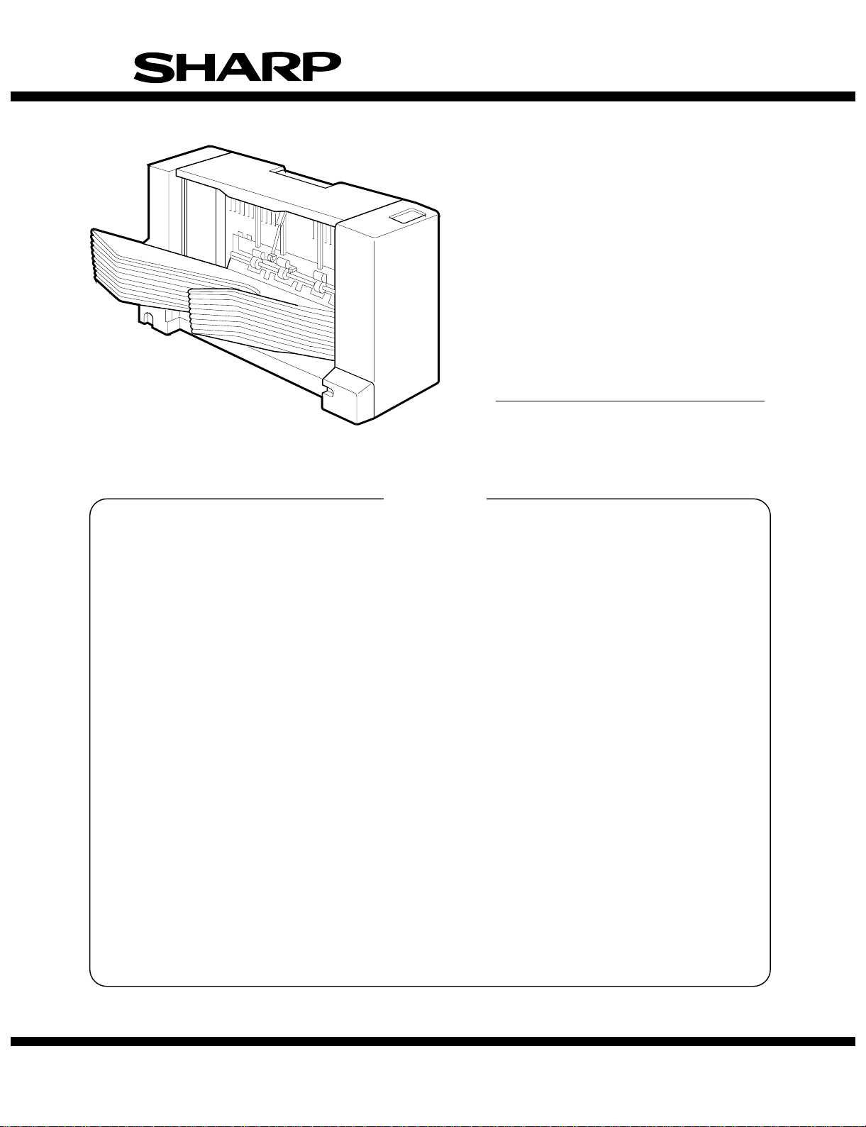
[1] SPECIFICA TIONS
(1) Type: Installation to a copier (hanging type)
(2) Distribution method: Bin shift by lead screws
(3) No. of bins: 10 bins (The top bin is used also for
non-sort.)
(4) Capacity of sheets: 30 sheets for each bin, (100 sheets for
the top bin)
When sorting A4 / 8-1/2 × 11″ 30 sheets
B4 / 8-1/2 × 14″ 20 sheets
A3 / 11 × 17″ 15 sheets
When grouping A4 / 8-1/2 × 11″ 20 sheets
B4 / 8-1/2 × 14″ 15 sheets
A3 / 11 × 17″ 15 sheets
(5) Paper size
Non-sort A3 ∼ A6 (Postcard) R / 11″ × 17″ ∼ 8-1/2″× 5-1/2″
Sort/group A3 ∼ A5 / 11″ × 17″ ∼ 8-1/2″× 11″
(6) Process capacity: 10 ∼ 30 sheets/min
(7) Paper transport: Center reference
(8) Paper collecting: Face up
(9) Paper weight
Non-sort 52 ∼ 128 g/m2 (14 ∼ 34 lbs)
Sort/group 56 ∼ 80 g/m2 (15 ∼ 21 lbs)
(10) Power source: Supplied from the copier body.
(11) External dimensions: 335 (W) × 493 (D) × 298 (H) mm
(12) Weight: About 7 kg
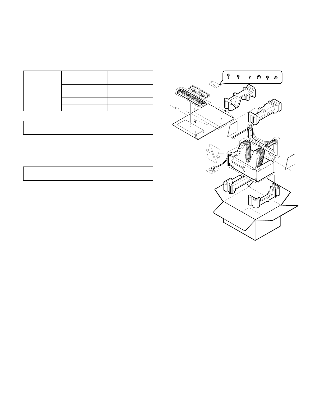
[2] UNP ACKING AND INSTALLATION
1. Unpacking
When unpacking, refer to the figure below.
– 1 –
Page 4
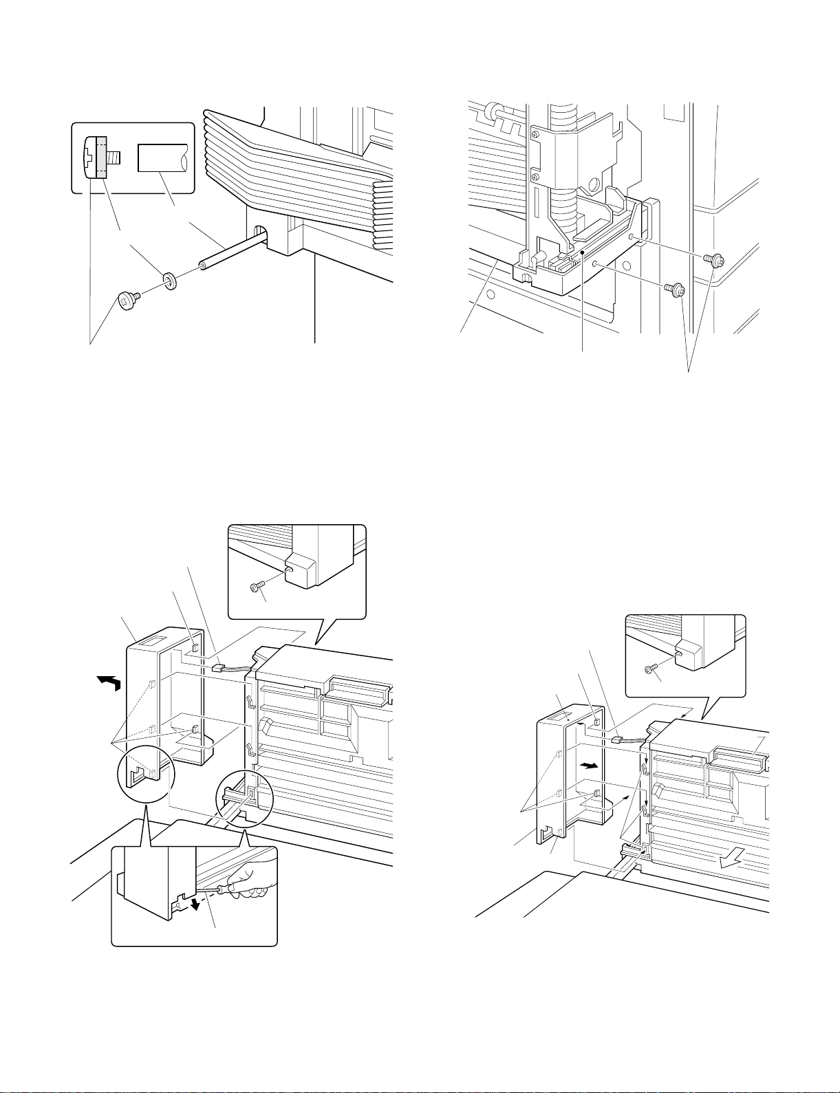
2. Installat ion
(5) SF-S18
Included parts
Support guide
(1 pc.)
Sorter seat cover securing screws
Sorter seat securing screws
(4 pcs.)
Spacers
(4 pcs.)
(3 pcs.)
Stopper screw
Lockplate screws (M4 x 8)
(2 pcs.)
Sorter securing screws (M4 x 8)
(2 pcs.)
Felt washer
(1 pc.)
(1 pc.)
Unplug the copier and follow the procedure below.
1. Mount the lock plate.
Remove the screws (2) from the upper side of the copier’s left cabinet
panel.
Mount the lock plate to the upper side of the copier’s left cabinet
panel and secure it with the M4 x 8 lockplate screws (2).
Upper left cabinet panel screws
Lock plate
(1 pc.)
Sorter seat
(1 pc.)
Sorter seat cover
(1 pc.)
Lock plate
Lock plate screws
2. Mount the support guide.
Hang the two hooks of the support guide on the exit area of the
copier to mount the support guide.
Hooks
– 2 –
Support guide
Page 5
3. Remove the cut-outs.
Remove the four cut-outs from the left cabinet panel of the copier.
Cut-outs
4. Insert the spacers.
Insert the four spacers into the holes which have been made by
removing the cut-outs in step 3.
6. Mount the sorter seat cover.
Mount the sorter seat cover to the sorter seat and secure it using
three sorter seat cover securing screws.
Sorter seat cover securing screws
Sorter seat cover
7. Mount the sorter.
Insert the shaft on the back of the sorter seat between the rollers at
the back of the sorter.
Back side
Spacers
Spacers
5. Mount the sorter seat.
Temporarily secure the sorter seat securing screws to the two upper
spacers which have been mounted in step 4.
Insert these two sorter seat securing screws into the two upper holes
of the sorter seat as shown in the figure.
Secure the lower part of the sorter seat by inserting the two sorter
seat securing screws into the lower two holes of the sorter seat and
tighten the temporarily secured upper screws to secure the sorter
seat.
Sorter seat securing screws
Rollers
Sorter
Sorter seat shaft
Next, insert the slide rail on the front of the sorter seat into the slide
rail mount on the front of the sorter and push the sorter in place.
Front side
Slide rail mount
Sorter
Sorter seat securing screws
Sorter seat
Sorter seat slide rail
NOTE:
Be sure to slide the sorter away from the copier and check that the
sorter is not removed from the slide rail of the sorter seat.
– 3 –
Page 6
8. Mount the stopper.
Mount the felt washer to the stopper screw and secure the screw to
the sorter seat shaft.
Shaft
Felt washer
Stopper screw
9. Remove the sorter’s front cabinet panel.
Remove the front cabinet panel screw.
Next, using a screwdriver, pry open the lower part of the front cabinet
panel to pull the lowest tab from the slot in which it is anchored.
Pull the front cabinet panel slightly up and out to remove it.
Disconnect the connector which is plugged into the front cabinet
panel.
Connector
Tab
Front cabinet panel
Front cabinet panel screw
10. Attach the sorter to the sorter seat.
Install the M4 x 8 sorter securing screws (2 pcs.) in the screw holes
on the sorter to attach the sorter to the sorter seat.
Sorter
Slide rail
Sorter securing screws
(M4 x 8)
11. Mount the sorter’s front cabinet panel.
Plug the connector from the sorter into the circuit board inside the
sorter’s front cabinet panel.
Fit the tabs on the left side of the front cabinet panel behind the ribs
on the sorter, and slide the tabs on the right-hand side of the front
cabinet panel behind the ribs in the sorter.
Check to be sure the tabs are securely positioned behind the ribs and
inserted properly into the slot.
Secure the front cabinet panel using the screw which was removed in
step 9.
Tab
Straight-edge screwdriver
Tab
Front cabinet panel
Circuit board
Tab
Connector
Tab
Front cabinet panel screw
Lock lever
Ribs
– 4 –
Page 7
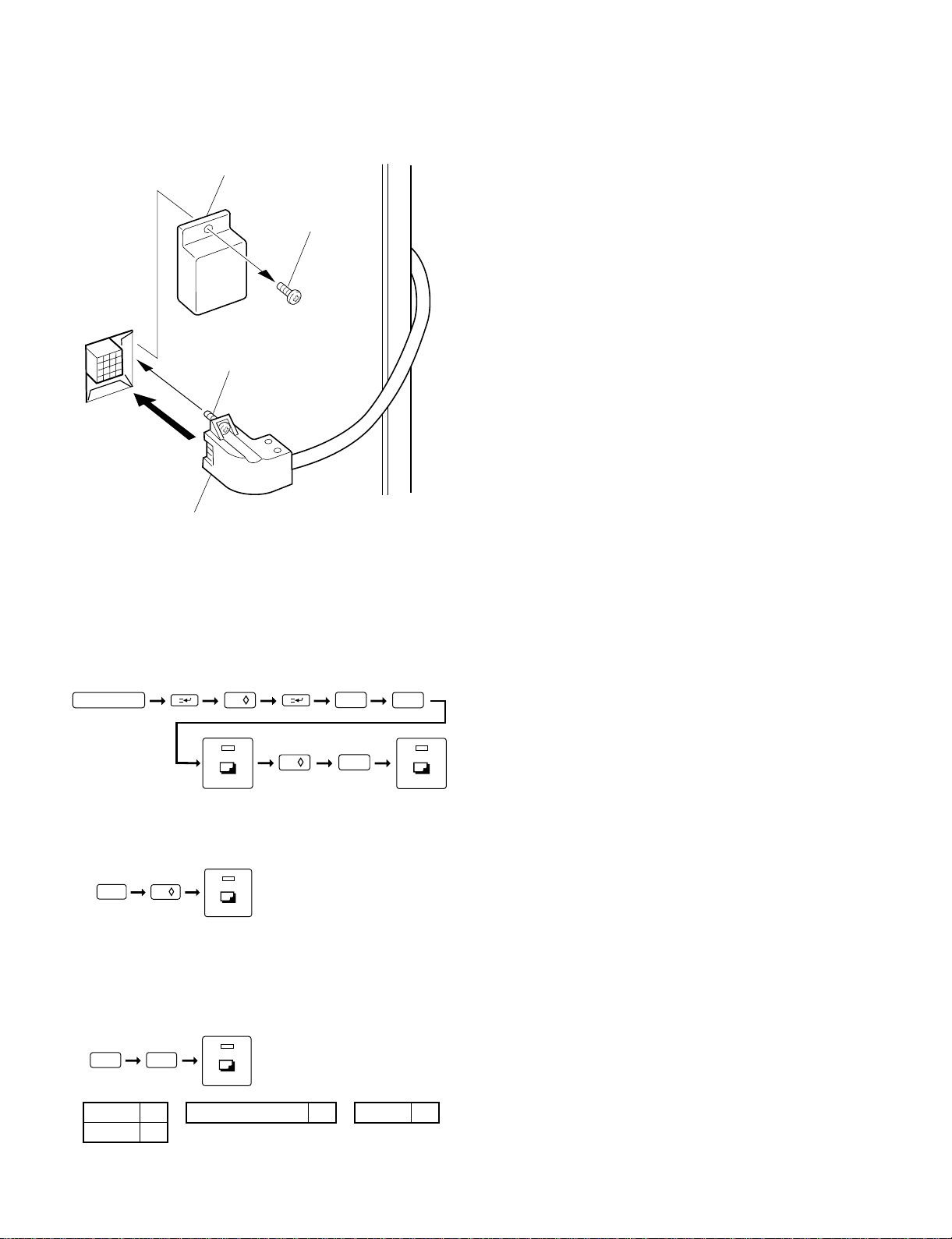
12. Connect the sorter connector.
Remove the sorter connector cover securing screw which is mounted
to the rear cabinet panel of the copier and remove the sorter connector cover.
Connect the sorter connector to the connector on the copier and
secure it using the sorter connector securing screw.
Sorter connector cover
Securing screw
Securing screw
Sorter connector
Plug the copier into a grounded outlet and turn the
power switch on.
Then, follow the procedure below.
13. Set the mode.
• Operate the copier keys to set the mode.
C
0/
0/
The above key operation will display the currently set mode.
2
6
1
• When only the SF-S18 is to be set, immediately after the above
key operation, operate the keys as follows:
1
0/
• If the mode is to be set in combination with other options, use the
table shown below to add up the total of the setting values for all
the peripheral devices to be set, and set that total value.
For example, if the SF-S18 and RADF are to be set, the total setting
value is 1 + 10 = 11.
Operate the keys as follows:
1
RADF 1 Stand/paper drawer 4 SF-S18 10
ADF 1
1
– 5 –
Page 8
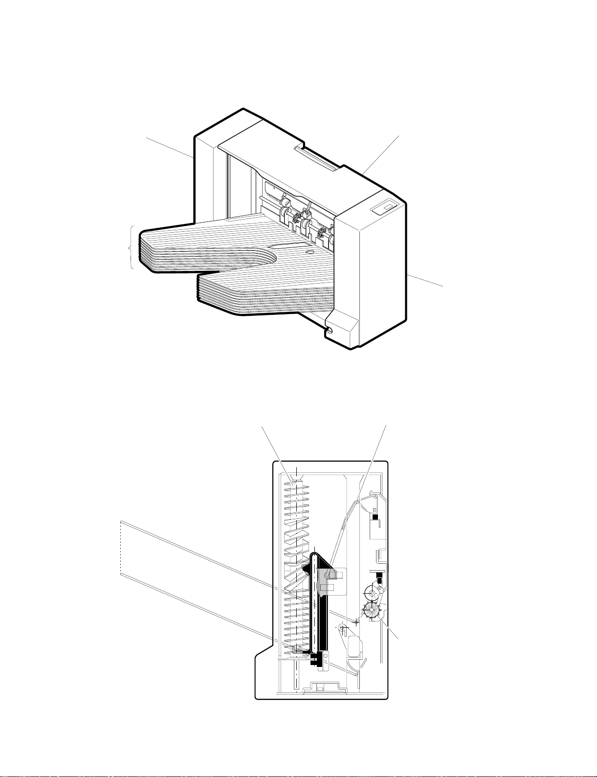
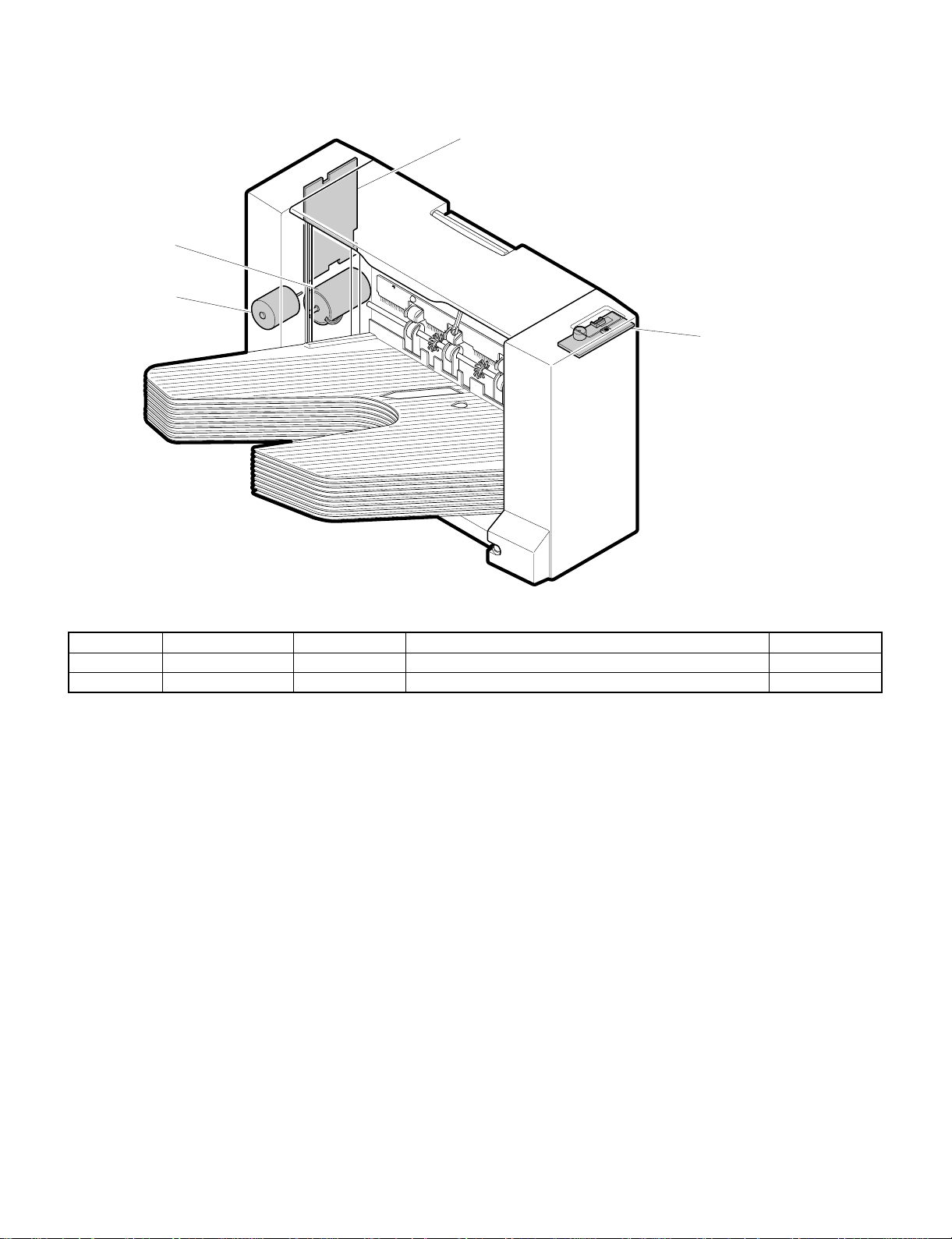
[3] PARTS IDENTIFICATION
1. External fittings
Rear cover
Trays
2. Mechanism section
Top cover
Fro nt co ve r
Spiral cam
Take-up SEN lever
Paper exit roller
– 6 –
Page 9
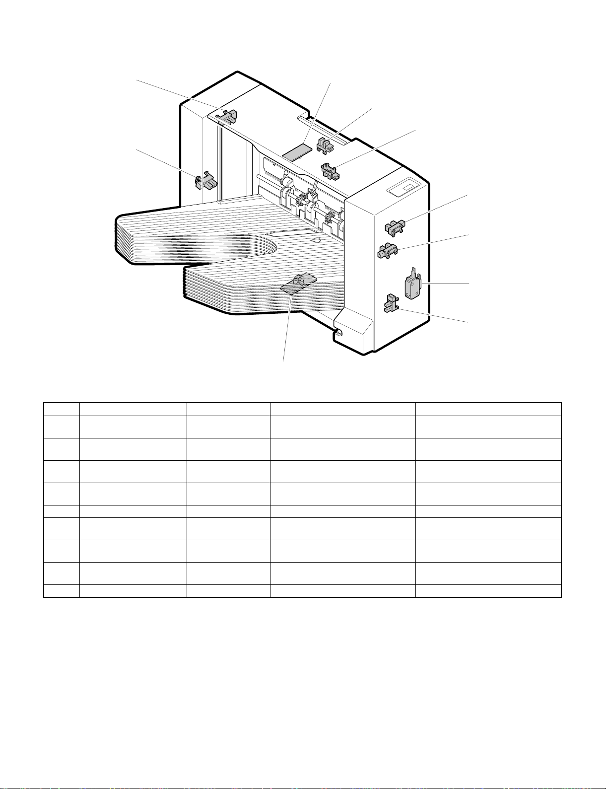
3. Sensors and switches
SEN7
SEN6
SEN5 (Light emitting)
SEN4
SEN1
SEN2
SEN8
SW1
SEN3
SEN5 (Light receiving)
Code Name Type Operation, function Contact, output
SEN1 Entry port sensor Photo interrupter Turns HIGH when the paper lead edge
reaches the transport roller.
SEN2 Bin home sensor Photo interrupter Used to sense the tray home position. HIGH when the home position is
SEN3 One rotation sensor Photo interrupter Used to sense the tray stop position. HIGH when the stop position is
SEN4 Take-up position sensor Photo interrupter Used to sense the paper take-up
position.
SEN5 Paper empty sensor Transmission sensor Used to sense the paper on the tray. LOW when the paper is sensed.
SEN6 Bin shift motor clock sensor Photo interrupter Used to sense rotation of the bin shift
motor.
SEN7 Transport motor clock
sensor
SEN8 Upper/lower limit sensor Photo interrupter Used to sense the tray limit position. HIGH when the limit position is
SW1 Sorter set switch Micro switch Used to sense the sorter installation LOW when the sorter is installed.
Photo interrupter Used to sense rotation of the transport
motor.
HIGH when paper is sensed.
sensed.
sensed.
LOW when the take-up position is
sensed.
Pulse output
Pulse output
sensed.
– 7 –
Page 10
4. Motors and PWB
M2
M1
Control PWB
Display PW B
Code Name Type Operation, function Contact, output
M1 Transport motor DC motor Used to shift the transport roller.
M2 Bin shift motor DC motor Used to drive the spiral cam for moving the tray up and down.
– 8 –
Page 11
[4] OPERATIONAL DESCRIPTIONS
1. Paper transport mechanism
The transport motor power is transmitted to the paper exit roller and
the paper feed roller.
Paper feed
direction
Paper exit roller
Paper feed roller
Transport motor
2. Bin up-down shift mechanism
The bin shift motor power is transmitted to the spiral cam 1 (R side)
by the timing belt and the gear, and to the spiral cam 2 (F side) at
the same time by the drive shaft.
The bin is shifted up or down by forword or reverse rotation of the
motor. The bin is stopped at the stop position by the one rotation
sensor attached to the spiral cam 2.
Down
Up
Spiral cam
2
Bin shaft
motor
Up
Down
Down
Up
Spiral cam
One rotation sensor
1
Paper exit
direction
Drive shaft
– 9 –
Page 12

3. Operatio n pr ocess
(Normal copy mode (Non-sort/sort/group))
START
STEP01
STEP02
First
paper exit bin
position
Curre nt bin position
≠
First
paper exit bin
position
> Current bin position
STEP03
STEP04
STEP05
STEP06
STEP07
First
paper exit bin
position
= Current bin position
STEP08
STEP09
STEP10
Copier START k ey ON
The operation mode (mo de, firs t paper
exit bin position) is received.
Transport motor ON
= Current bin position
→
to
1
< Current bin position
→
To STEP 11
Bin motor lowering rotation
One rotation sensor OFF
One rotation sensor ON
One rotation sensor OFF
One rotation sensor ON
> Current bin position
To STEP 04
→
Bin stop position correction pulse set
Bin stop position correction pulse up
Bin motor stop
<Operation mode reception, transport motor ON,
paper exit roller rotation>
Bin
Follower roller
Paper exit roller
One rotation sensor
to 1
STEP11
STEP12
STEP13
STEP14
STEP15
First
paper exit bin
position
= Current bin position
To STEP 08
Bin motor lifting rotation
One rotation sensor OFF
One rotation sensor ON
One rotation sensor OFF
One rotation sensor ON
< Current bin position
→
To STEP 12
– 10 –
Page 13

1
Group mode
No
Sort mode
No (Non-sort mode)
STEP 1 6
STEP 17
STEP 1 8
Next paper
No
To STEP 42
STEP 1 9
STEP 2 0
STEP 2 1
To 2
2
YES
→
To STEP 31
YES
→
To STEP 19
Copier paper exit comman d rec ept i on
Sorter entry p o rt sensor O N
Sorter entr y port sens or O F F
YES
→
To STEP 16
Copier paper exit comman d rec ept i on
Sorter entry p o rt sensor O N
Sorter entry port sensor OFF
<Copy paper entry sensor passing, sensor ON>
Bin
Entry port
sensor ON
Copy paper
Paper exit roller
Next paper
YES
Folding
command
NO
Sorting
directi o n
Reverse sorting
STEP 2 2
STEP 23
STEP 2 4
STEP 25
STEP 2 6
STEP 27
STEP 2 8
STEP 2 9
To STEP 19
STEP 3 0
NO
→
To ST EP 4 2
YES
To ST EP 1 9
→
Normal sorting
→
To ST EP 3 0
Bin motor lifting rotation
One rotation sensor OFF
One rotation sensor ON
One rotation sensor OFF
One rotation sensor ON
Bin stop position correction pulse set
Bin stop posi tion c or recti on pu lse up
Bin motor stop
Bin motor lower i ng r otat ion
<Copy paper entry port sensor passing, sensor OFF>
Bin
Copy
paper
Entry port
sensor OFF
Paper exit
roller
To STEP 23
STEP 3 1
STEP 3 2
STEP 3 3
Next paper
YES
To 3
Copier paper exit comman d rec ept i on
Sorter entry p o rt sensor O N
Sorter entr y port sens or O F F
NO
→
To ST EP 4 2
– 11 –
Page 14

3
Bin shift
command
NO
→
YES
STEP 34
STEP 35
STEP 36
STEP 37
STEP 38
STEP 39
STEP 40
STEP 41
Bin lowering rotation
One rotation sensor OFF
One rotation sensor ON
One rotation sensor OFF
One rotation sensor ON
Bin stop position correction pulse set
Bin stop posi t i on corre cti on pul se up
Bin motor stop
To STEP 31
STEP 42
Transport motor stop
END
(Take-up mode)
START
STEP 01
Paper
present on
Take-up mode start command reception
Paper empt y
tray
→
Paper present
To STEP 31
STEP 21
<Paper exit completion - transport motor stop -
paper exit roller stop>
Copy paper
<Take-up mode reception - take-up home position>
Current
bin position
< Take-up home position
STEP 02
STEP 03
STEP 04
Current
bin position
1
Take-up
sensor
Bin lifting rotation
One rotation sensor OFF
One rotation sensor ON
= Take -up home po si tion
OFF
STEP 05
STEP 06
STEP 07
STEP 08
One rotation sensor OFF
One rotation sensor ON
One rotation sensor OFF
One rotation sensor ON
To 1
STEP 09
STEP 10
STEP 11
STEP 12
Bin stop position correction pulse set
Bin stop posi t i on corre cti on pul se up
Bin motor stop
Tray pape r tak e- up
> Take-up ho me p osition
→
STEP 14
> Take-up ho me p osition
→
STEP 03
> Take-up ho me p osition
→
STEP 9
To 2
– 12 –
Page 15

2
Take-up
sensor
ON
→
OFF
Tray paper
present
Paper empty
→
Paper present
STEP 13
Bin motor lifting rotation
To STEP 05
STEP 14
STEP 15
STEP 16
Current
bin posi tion
Bin motor l owe ri ng rotation
One rotation sensor OFF
One rotation sensor ON
Take-up home po s it i on
→
= Take -up home po si tion
STEP 17
STEP 18
STEP 19
STEP 20
Bin stop position correction pulse set
Bin stop posi t i on corre cti on pul se up
Bin motor stop
Tray pape r tak e- up
To 2
To STEP 12
To STEP 21
To STEP 15
<Take-up mode completion - bin home position>
STEP 21
STEP 22
STEP 23
STEP 24
STEP 25
STEP 26
END
Bin motor l owe ri ng rotation
Bin home sens or ON
One rotation sensor ON
Bin stop position correction pulse set
Bin stop posi t i on corre cti on pul se up
Bin motor stop
– 13 –
Page 16

[5] DISASSEMBLY AND ASSEMBLY
No. Item
1 External fitting removal 13
2 Paper exit roller removal 14
3 Spiral cam and tray removal 14
4 Discharge brush removal 16
5 Interface cable removal 16
6 Control PWB removal 17
Motor bracket unit removal
7
(Transport motor and bin shift motor)
Bin shift motor clock sensor and transport motor
8
clock sensor removal
Bin home sensor and upper/lower limit sensor
9
removal
10 One rotation sensor removal 18
Take-out position sensor and entry port sensor
11
removal
12 Paper empty sensor upper removal 19
13 Paper empty sensor lower removal 19
Ref.
page
17
18
18
18
1. External fitting removal
(1) Remove screw A and connector B, and remove front cover C.
(In the sequence of 1, 2, 3 and 4.)
(2) Remove screw D, and remove rear cover E. (In the sequence
of 1, 2, 3, and 4.)
(3) Remove connector F, and remove top cover G.
(4) Remove screw H and remove harness cover I in the se-
quence of 1, 2, 3.
G
D
E
F
B
4
A
4
C
2
1
2
3
Screwdriver
3
– 14 –
Page 17

Rear side
(2) Remove take-up SEN lever A.
1
2
3
Front
side
H
2. Paper ex it roller removal
(1) Remove the harness cover. (Refer to procedure 1 - (4).)
(2) Remove connection cover A.
(3) Remove paper exit roller B.
I
A
(3) Remove lever B from tray collar 2 C.
B
C
A
B
Radio nipp ers
3. Spiral cam and tray remo val
(1) Remove the front cover, the rear cover, and the top cover.
(Refer to procedure 1.)
(4) Remove timing belt D and worm support frame E, and remove
worm gear F.
(5) Manually turn the spiral cam to lower the tray to the bottom.
(Lower than the the home position.)
Loosen the screw.
Tensioner
Timing belt
– 15 –
Page 18

(6) Remove cam bush G, and remove spiral cam H and I.
(7) Remove the tray.
E
Rear side
I
D
F
G
(Assembly)
(8) Assemble spiral cams H and I. Be sure to fit the phases of
both cams.
To fit the phases, use the hole at the center of each spiral
°
cam. Set so that the same shape (round or square) faces
towards you. Look into the front hole through the rear hole,
and set spiral ass’y F.
Front side
G
Front side Rear side
* Be sure to check that the shapes of the holes at the centers
of spiral cams H and I are the same.
• Check that you can see thorough the front hole and the
rear hole.
(9) Turn spiral cam H or I to lower the tray, and insert trays one
by one.
* Be careful not to skip any bin position.
H
– 16 –
Page 19

(10) When the tray reaches the home position, attach the lever which
was removed in procedure (3) to the tray collar.
(11) For the assembly hereinafter, reverse the disassembly proce-
dures. ((5) (4) (3) (2) (1))
4. Discharge bru sh re moval
(1) Remove the timing belt, turn the spiral cam manually to put the
tray at the bottom. (Refer to procedure 4.)
(2) Remove screw A, and remove discharge brush B.
6. Control PWB removal
(1) Remove the rear cover. (Refer to procedure 1.)
(2) Remove the interface cable. (Refer to procedure 6.)
(3) Remove screw A and all connectors from control PWB B, and
remove control PWB B.
B
A
A
A
B
5. Interface cable removal
(1) Remove the rear cover. (Refer to procedure 1.)
(2) Remove connectors A and B, screw C, and grounding screw
D, and remove the interface cable E.
B
A
* When removing connectors of the PWB, be sure to turn off the
power in advance.
7. Motor bracket removal (Transport
motor & bin shift motor)
(1) Remove the rear cover. (Refer to procedure 1.)
(2) Remove the interface cable. (Refer to procedure 6.)
(3) Remove screw A and connectors, and remove harness bracket
B.
(4) Remove timing belt C and screw D, and remove motor bracket
unit E.
D
C
E
– 17 –
Page 20

8. Bin shift motor clock sensor and
transpor t moto r clock sen sor rem o val
(1) Remove the rear cover. (Refer to procedure 1.)
(2) Remove screw A (commonly tighten with the grounding ter-
minal) and connector B, and remove bin shift motor clock sen-
sor C.
(3) Remove screw D and connector E, and remove transport
motor clock sensor F.
E
D
C
* When removing the timing belt, loosen the screw shown
below and loosen the tensioner.
A
A
B
Loosen the screw.
Tensioner
Timing belt
F
D
A
E
C
B
9. Bin home sensor and upper/lower limit
sensor removal
(1) Remove the font cover. (Refer to procedure 1.)
(2) Remove screw A, and remove harness bracket B.
(3) Remove screw C and remove HP-LIM sensor bracket D.
(4) Remove bin home sensor E (white connector) and upper/lower
limit sensor F (black connector).
A
– 18 –
B
A
E
F
C
C
* Be careful not to mistake the bin home sensor for the
upper/lower limit sensor. The connectors are different from
each other to prevent mistaken connection.
D
Page 21

10. One rotation sensor removal
12. Paper empty sensor upper removal
(1) Remove the front cover. (Refer to procedure 1.)
(2) Remove screw A and connector B, and remove one rotation
sensor C.
B
C
A
11. Take-up position sensor and entry
port sensor removal
(1) Remove the harness cover. (Refer to procedure 1.)
(2) Remove screw A, and remove take-up position sensor B.
(3) Remove connection cover C.
(4) Remove entry port sensor D.
(1) Remove the top cover. (Procedure 1.)
(2) Removes crew A, and remove cover B.
C
B
A
A
(3) Remove paper empty sensor upper C (transmission sensor).
13. Paper empty sensor lower removal
(1) Put the sorter on the side.
(2) Remove screw A, and remove cover B.
(3) Remove paper empty sensor lower C (transmission sensor).
D
C
* Be careful not to mistake the take-up position sensor and the
entry port sensor. The connectors are different from each
other to prevent mistaken connection.
Rear side
B
Connctor
Front side
A
C
B
A
– 19 –
Page 22

[6] ADJUSTMENTS
1. Single unit test mode
To enter the single unit test mode, keep the push switch on the
control WPB pressed and supply the power. After entering the single
unit test mode, select the kind of single unit tests with the DIP switch.
Selection of the kind of single unit tests is made by turning on/off the
sorter joint switch.
Setting of buzzer sound in the take-up mode
Use the DIP switch on the control PWB to set the buzzer sound.
Push switch DIP switch
ON
DIP
DIP
DIP
DIP
SW2
SW1
DIP SW4 Operation
ON Buzzer sound ON
OFF Buzzer sound OFF
* DIP SW1 ∼ 3 and the pu sh switch ar e used in the in dividual un it
test mode. For details, refer to [6] ADJUSTMENTS.
2. Starting the single unit test mode
After entering the single unit test mode, push the push switch on the
control PWB to start the test.
To finish the pa per feed m ode, push the switch.
3. Kinds of single unit test modes
Mode DIPSW3 DIPSW2
(1) Non-sort paper feed mode OFF OFF OFF
(2) Sort paper feed mode OFF OFF ON
(3) Group paper feed mode OFF ON OFF
(4) Load operation mode OFF ON ON
(5) Sensor check mode ON OFF OFF
(6) No paper aging mode ON OFF ON
No paper aging mode
(7)
(without speed control)
ON ON OFF
SW3
SW4
DIPSW1
(3) Group paper feed mode
Press the push switch on the control PWB to start. (The transport
motor is turned on.)
After the transport motor is activated, press the push switch on the
display PWB to set the number of groups. (Pressing the push switch
shifts the number from 5, 10, 15, and 20 in this sequence.)
Press the push switch on the control PWB again to finish the operation.
(4) Load operation mode
Used to check each load output. Press the push switch on the control
PWB to start and select each output step in the following sequence.
Turning on/off the joint switch finishes the operation.
1 Transport motor ON
2 Transport motor OFF
3 Bin motor forward rotation (shift bin up)
4 Bin motor OFF
5 Bin motor reverse rotation (shift bin down)
6 Bin motor OFF
7 Buzzer ON
(5) Sensor check mode
Each sensor operation can be checked with the buzzer sounds.
Press the push switch on the display PWB to check each sensor in
the following sequence. The buzzer is turned OFF when the sensor
senses.
1 Bin home sensor
2 Entry port sensor
3 Take-out position sensor
4 Paper empty sensor
5 One rotation sensor
6 Upper/Lower limit sensor
(6) No paper aging mode
The sort mode operations from No. 1 bin to No. 10 bin are performed
in a certain tim ing.
Press the push switch on the control PWB to start and finish the
operation.
(7) No paper aging mode (without speed control)
The operation of the no paper aging mode is performed without
speed control of the motors (at full speeds).
4. Description on each mode
(1) Non-sort paper feed mode
Press the push switch on the control WPB to start. (The transport
motor ON.)
When paper is loaded, it is dischar ged onto the first bin.
Press the push switch again to finish the operation.
(2) Sort paper feed mode
Press the push switch on the control PWB to start. (The transport
motor is turned ON.)
After the transport motor is activated, press the push switch on the
display PWB to set the number of bins for sorting. (The number of
bins can be checked with the buzzer sounds.)
Press the push switch on the control PWB again to finish the operation.
5. Setting of buzzer sound in the take-u p
mode
Set the DIP switch 4 as follows:
DIP SW4 Operation
ON Buzzer sound ON
OFF Buzzer sound OFF
– 20 –
Page 23

[7] MAINTENANCE
[Note] ★ Lubricate, | Clean, ∆ Adjust, ▲ Replace,
✕ = Check. (Clean, replace, adjust as necessary.)
Part name 50K 100K 150K 200K Same cycle afterward
Feed roller H (Paper exit roller) ||||
Sensors ||||
Worm gear (for shifting bin) Grease Grease
Worm gear (for transport) Grease Grease
Timing belt ||||
Transport motor
Bin motor
Replace at 500K.
[8] TROUBLESHOOTING
[A] The sorter does not operate. (Except
for pape r jam)
A
Is the interface
cable pro perl y
connected?
YES
Is DC5V
applied between
CN2,3 p in &
4 pin?
YES
Is DC24V
applied between
CN2,1 p in &
2 pin?
YES
Does the
transport motor
rotate normally?
NO
NO
NO
NO
Connect the inte r face
cabl e properly
Is DC24V
applied between
CN2,1 p in &
2 pin?
NO
Replace t he
interfac e cable
[C] Transport motor check
YES
Check the
copier power
source
[B] Transport motor error
B
Is the load
of the motor shaft
mormal?
YES
Is the motor
winding shorted?
NO
Is DC24V
applied Between
CN7,1 pin &
2 pin?
YES
Is the
harness prope rly
connect ed?
YES
Adjust the mechanism loads and the driv e
NO
system, and remove foreign materials
YES
NO
NO
Replace the mot or
Check or replace
the control PWB
harness prope rly
Connect the
YES
Does the
bin shift m oor
rotate mormally?
YES
Check or r eplace
the contr ol P WB
NO
[C] Bin shift motor check
– 21 –
Is the motor
clock sensor
output normal?
YES
Check or replace the
control PWB
NO
Check the motor clock s ensor
output or replace it
Page 24

[C] Bin shift motor error [D] Communication error
C
Is the load of
the motor shaft
normal?
YES
Is the motor
winding shorted?
NO
Is DC24V
applied between
CN8,1 pin and
2 pin?
YES
Is the harness
connected
properly?
YES
Is the motor
clock sensor
outpu t n orm al?
Adjust the mechanism loads and the driv e
NO
syatem, and remove foreign materials
YES
NO
NO
NO
Replace the mot or
Check or replace
the control PWB
Connect the
harness prope rly
Check the motor clock s ensor
output, or replace it
D
Is the
interfac e cable
normal?
YES
Check or r eplace
tne contr ol P WB
Is it OK?
YES
Check or r eplace
the contr ol P WB
NO
NO
Replace t he
interfac e cable
Check or replace the
main body PPC PWB
YES
Is the bin at the
upper or lower
limit posit ion?
YES
Are the
home senso r ou tpu t
and the limit sensor
output nor ma l?
YES
Check or replace
the control PWB
Manually move the bin from
NO
the limi t position
NO
Check or replace the home
sensor and the limit sensor
– 22 –
Page 25

[9] ACTUAL WIRING DIAGRAMS
Take-up position sens or
(SEN4)
Entry port
sensor
(SEN1)
AIM main harness
ass'y
Transpor t moto r
(SEN7)
Transp o r t mo tor
clock sensor
(SEN5)
Bin shift m ot or (M 2)
Control PWB
(PBA-CONTROL)
AIM-INT
harness
Bin shift
motor clock
sensor
(SEN6)
AIM-CN008 ass'y
Display PWB
(PBA-OPPANEL)
Upper/lower
limi t sens or
(SEN8)
One rota tion sensor
(SEN3)
Bin home sensor
(SEN2)
Sorter set SW
(SW1)
Paper empty
sensor PWB
(PBA-PT43)
AIM-CN005 ass'y
Paper empty
sensor PWB (LED)
(PBA-LR43)
AIM-CN005 ass'y
– 23 –
Page 26

[10] CIRCUIT DESCRIPTIONS
1. Summary
This control circuit is used to pick up the paper discharged from the main body and distribute to one of trays 1 ∼ 10. It is c omposed of sensors ,
switches, the circuit which processes inputs from the PPC, the circuit which drives the motors, the CPU, and its peripheral circuits.
2. Block diagra m
Control PWB
Copier bo dy
interface section
Entry port sensor
Bin home sensor
One rotation s e nsor
Take out position
sensor
Paper empty LED
Paper empty sensor
Bin shift moto r clock
sensor
Transport motor clock
sens or
Upper/Lower limit
sensor
SEN1
SEN2
SEN3
SEN4
SEN5CLK
SEN5
SEN6
SEN7
SEN8
Serial interface
section
Entrance sensor
input section
Bin home sensor
input section
One rotation s e nsor
input section
Take out position sensor
input section
Paper empty LED CLK
output sec t i on
Paper empty sensor
input section
Bin shift motor clock senso r
CLK input section
Transport motor clock sensor
CLK input sec t ion
Upper/Lower limit sensor
input section
SEN1
SEN2
SEN3
SEN4
SEN5CLK
SEN5
SEN6
SEN7
SEN8
System reset
section
CPU
LATCH
Display section LOGIC
Transpor t motor (M1)
control se ct ion
Bin shift motor (M2)
control section
ROM
256K
Display
PWB
M1
Transpor t motor (M1)
M2
Bin shift motor (M2)
Sorter set switch
Main body power
source
SW1
DC24V
DC5V
System cl oc k
secti on
Sorter set swit ch
input section
Power input section
SW1
– 24 –
Page 27

3. Operation
A. Communication circuit
This circuit is used to communicate with the copier body.
+5V
+5V
R8
R6
470
JINT
4
3
1
2
5
6
7
8
CN1,4 TXD
CN1,3 RXD
CN1,1 DTR
CN1,2 DSR
CN1,5 RESET
CN1,6 SGND
CN1,7
CN1,8 N.C
The input and the output of each signal are as follows:
[a] DTR CN1-1 pin
The input from the main body. When LOW (0V) at IC11-4 pin, it means the main body has the control to transmit.
[b] DSR CN1-2 pin
The output in the sorter side. When HIGH (+5V) at IC11-3 pin, IC11-4 pin turns from LOW (0V) to HIGH (+5V) then to LOW again. During that
period, the sorter has the control to transmit.
[c] TXD CN1-4 pin
The input from the main body. When IC11-79 pin turns from HIGH (+5V) to LOW, data reception is started.
[d] RXD CN1-3 pin
The output in the sorter side. When IC11-80 pin turns from HIGH (+5V) to LOW, data transmission is started.
[e] RESET CN1-5 pin
The reset signal from the main body. When CN1-5 pin is HIGH (+5V), the CPU (IC11) is reset.
R7
4.7K
R64
100
R63
100
R62
100
SGND SGND
C20
100PF
C16
100PF
Test pat30
C2
0.10µF
Test pat23
Test pat29
IC2.2
34
HD74HC14FP
IC2.3
HD74LS06FP
6
5
HD74HC14FP
HD74HC14FP
4
IC2.1
12
IC6.1
12
IC6.2
3
HD74LS06FP
Test pat31
Test pat24
VCC-+5V
GND-SGND
11 10
HD74LS06FP
IC6.5
R59
4.7K
IC6.3
6
HD74LS06FP
Test pat25
+5V
R74
10K
5
Test pat26
Test pat27
Test pat28
Test pat35
IC11
79
80
4
3
Main body reset
B. Reset circuit
This circuit is the reset circuit.
D1
RES
VS
SGND
2
7
DSA010
*RES
VREF
C22
470PF
CK
CT
C23
0.10µF
+5V
5
VCC
4
GND
IC5
MB3773 FP
This circuit is used to generate the CPU reset signal, and is composed of IC5 and its peripheral circuits.
+5V
KA
R72
10K
3
8
C17
1µF
Test pat33
1
6
19
HD74LS06FP
+
IC6.4
+5V
R75
10K
8
Test pat64
2
IC7.1Y
3
HD74HC02FP
VCC-+5V
GND-SGND
Main body reset
6
IC11
1
7
– 25 –
Page 28

IC5 has integrated reset functions including the power on reset, the +5V abnormal fall reset, and the watch dog timer function.
When the power line reaches about 0.8V by turning on, IC5 starts operation and IC5 8 pin becomes LOW to reset the CPU. The reset state is
maintained until a certain time is passed after power line’s reaching about 4.3V. The reset maintaining time id determined by the capacity of C17. It
is about 100msec for this circuit. After passing the reset time, IC5 8 pin turns to HIGH to cancel reset, and the CPU resumes operation.
When the power line voltage falls to about 4.2V, IC5 8 pin turns to LOW to issue the reset signal, and the reset state is maintained as far as the
power voltage is lower than about 4.3V. After about 100msec from when the power voltage reaches about 4.3V, reset is cancelled.
IC5 3 pin is the watch dog timer clock sinal input pin, and the output signal from the CPU 6 pin is used as the clock. When the CPU normally
operates, the clock is regular pulse signal of 50% duty and 5msec frequency. When the CPU is hung up or in an abnormal state, the clock is not
supplied. IC5 normally monitors this clock. When the clock supply is stopped, after a ceratin time, IC5 drives 8 pin to LOW to supply the reset signal.
The monitoring time of clock is determined by the capacity of C17, and is about 100msec for this circuit.
Hard reset is also applied from the PPC through the communication cable. In this case, CN1-5 pin is driven to HIGH or opened to reset.
C. Sensor input circuit
[a] Tray paper empty sensor (SEN5) circuit
Test pat14
Paper empty sensor
LED(SEN5)
Paper empty sensor
PHTr(SEN5)
Light
receiving
circuit
Light
emitting
circuit
CN4,2
CN4,1
SEN5_CLK
CN5,1
CN5,2
CN5,3
+5V
+5V
SEN5
SGND
2
1
+5V
1
2
3
SGND
+5V
2.0K
+5V
R58
200K
C6
0.10µF
2SC2712
Test pat22
C
E
SGND
+5VR50
R51
100K
BQ2
R67
4.7K
R31
10K
Test pat21
Test pat15
+5V
Test pat63
R52
3.6K
R53
12K
SGND
R56
4.7K
3
+
2
-
µPC393G2
VCC-+5V
GND-SGND
Test pat16
R54
56K
1
IC9.1
IC12.5
10
HD74HC14FP
Test pat17
+5V
R40
4.7K
Test pat20
11
+5V
+5V
IC3.1
4
*PR
3
CLK
2
D
1
*CLR
HD74HC74FP
VDD-+5V
GND-SGND
R71
10K
5
IC11
5
Q
6
*Q
62
Test pat18
This circuit is used to sense the presence of paper on the tray. CN4 is connected to the light emitting PWB, and CN5 is connected to the light
receiving PWB.
1. Light emitting circuit
The signal outputted from the CPU (IC11-5 pin) at a certain frequency is inputted to IC12-11 pin, and the reversed output is inputted to the base of
Q2. Consequently Q2 turns on to light the LED.
2. Light receiving circuit
(1) Light receiving PWB circuit
1
VCC
C
PT1
ST-1KL3A(CD)
E
Q2
2SC2712GRBL
C
B
E
R3
1.0K
R1
10K
C1
0.01µF
16K
2
C4
0.47µF
3
GND
C
Q1
B
2SC2712
E
R2
0.010µF
R4
4.7K
R7
100K
R6
390
B
C
Q3
2SC2712GRBL
E
C3
10µF
C2
R5
16K
VOUT
GND
CN1,1
CN1,2
CN1,3
The photoelectric current flowing through PT1 becomes the base current of Q1 and operates Q1 and is converted into the output voltage by R4. Part
of current flowing through Q1 is integrated by R2 and C1 and is passed to the base of Q2 to set the operating point of Q1 with Q2, PT1, and R3.
(The collector potential of Q2 is set to about 1.2V)
When disturbance lights (DC light, fluorescent light, etc.) enters the light receiving element, the DC current in PT1 and Q1 tries to increase according
to the disturbance lights. However, this current is passed through R2 to the base of Q2, conducting Q2. Therefore, the photoelectric current
generated by disturbance lights becomes the collector current of Q2, and does not flow to the base of Q1 which has a higher impedance. In this
manner, an increase in the Q2 collector current is suppressed, and the operation is controlled. (When disturbance light increases, the Q2 emitter
voltage increases by R3, therefore the limit of voltage for normal operations is about 2.5V or less. If there is no disturbance light, it is set to about
0V.)
When the signal light becomes too intense, the same control is performed.
R2 and C1 forms the low pass filter which allows the fluorescent light completely to pass and does not allow modulated light to pass.
– 26 –
Page 29

3. Control PWB light receiving circuit
+5V
R71
CN5,1
CN5,2
CN5,3
+5V
SEN5
SGND
1
2
3
SGND
+5V
2.0K
+5V
C6
0.10µF
Test pat22
10K
Test pat17
+5V
R40
4.7K
1
Test pat20
+5V
4
3
2
1
HD74HC74FP
VDD-+5V
GND-SGND
IC3.1
*PR
CLK
D
*CLR
5
Q
6
*Q
+5VR50
R51
100K
R67
4.7K
R52
3.6K
Test pat21
+5V
SGND
Test pat63
R53
12K
R54
56K
3
+
2
-
IC9.1
µPC393G2
VCC-+5V
GND-SGND
5
IC11
62
Test pat18
The signal outputted from the light receiving PWB is DC-cut by C6 and modulated by the comparator (IC9). (It is digitally converted by the
comparator, and the threshold value of the comparator is about 3.8V.)
The digital signal outputted from the comparator is latched by the flip-flop (IC3).
When D (2 pin) is HIGH at the rising edge of CLK (3 pin) of the flip-flop (IC3), it is judged as "no paper" and the output Q (5 pin) becomes HIGH.
When D (2 pin) is LOW (0V), it is judges as "paper present" and the output Q (5 pin) becomes LOW.
[b] Bin home sensor (SEN2) circuit
Entry port sensor (SEM1) circuit
One rotation sensor (SEN3) circuit
Take-out position sensor (SEN4) circuit
Upper/lower limit sensor (SEN8) circuit
1) The bin home sensor (SEN2) circuit is used to sense that the tray is at the paper exit position of the first bin.
The sensor is of the photo transmission type (photo interrupter), and includes the LED and the photo transistor. The output level is normally LOW
(0V) because of light transmission.
When the tray reaches the paper exit position of the first bin,the LED light is interrupted and the output of the photo transistor becomes HIGH
(+5V).
Then the HIGH output is inputted to CN10-10 pin, and the converted LOW output (0V) is inputted to IC11-59 pin.
2) The Entry port sensor (SEM1) circuit is used to sense that the paper discharged from the PPC enters the sorter entrance .
After sensing, it operates in the same manner as the home sensor. The signal is inputted to IC11-60 pin.
3) The one rotation sensor (SEN3) circ uit is used to sense that the tray is at a position suitable for paper exit or take-up.
The sensor is of the photo transmission type (photo interrupter), and includes the LED and the photo transistor. The output level is normally LOW
(0V) because of light transmission.
When the lead cam reaches the stop position, the LED light is interrupted and the photo transistor output becomes HIGH (+5V).
Therefore the HIGH level output is inputted to CN10-13 pin, and its signal is inputted to IC11-72 pin.
4) The take-out position sensor (SEN4) circuit is used to sense that the paper on the tray is at the take-up position in take-up mode.
The sensor is of the photo transmission type (photo interrupter), and includes the LED and the photo transistor. The output level is normally LOW
(0V) because of light interruption.
When the paper reaches the take-up position, the LED lights in interrupted, and the photo transistor output becomes HIGh (+5V).
Therefore the HIGH level output is inputted to CN10-3 pin, and the converted LOW signal is inputted to IC11-61 pin.
It is about 1.2V by monitoring through connection between CN10-1 pin and IC11-63 pin, but becomes HIGH (+5V) when open.
– 27 –
Page 30

5) Upper/lower limit sensor (SEN8) circuit is used to sense that the bin reaches the upper or lower limit by an overrun or an abnormal operation.
The sensor is of the photo transmission type (photo interrupter), and includes the LED and the photo transistor. The output level is normally LOW
(0V) because of light interruption.
When the bin reaches the upper or lower limit, the LED transmits light and the photo transistor output becomes HIGH (+5V).
Therefore the HIGH level output is inputted to CN9-2 pin and the converted LOW output (by IC12 is inputted to IC11-56 pin.
3
VCC
Bin home sensor
(SEN2)
S2
GP1S74P
Entry port sensor
(SEN1)
S1
GP1S74P
Take-out position
sensor (SEN4)
S4
GP1S74P
One rotation
sensor (SEN3)
S3
GP1S74P
Upper/lower limit
sensor (SEN8)
S8
LG203D-3
VOUT
GND
VCC
VOUT
GND
VCC
VOUT
GND
VCC
VOUT
GND
VCC
VOUT
GND
1
2
3
1
2
3
1
2
3
1
2
1
2
3
CN10,7
CN10,8
CN10,10
CN10,9
CN10,4
CN10,6
CN10,5
CN10,1
CN10,3
CN10,2
CN10,11
CN10,13
CN10,12
CN3,1
CN3,2
CN3,3
N.C
SEN2AN
SEN2
SGND
SEN1AN
SEN1
SGND
SEN4AN
SEN4
SGND
SEN3AN
SEN3
SGND
+5V
SEN8
SGND
+5V
430 x 4
7
R34
8
R68
10
9
4
6
5
1
3
2
11
13
12
1
2
3
SGND
+5V
30K x 4
10K
Test pat1
R16
R61
R69
R43
SEN4AN
R28
R42
R41
R29
10K
Test pat2
R39
10K
Test pat3
R38
10K
Test pat4
R37
10K
Test pat7
R15
10K
C3 C7 C12 C1 C5
SGND
0.010µF
x 5
IC12.1
HD74HC14FP
IC12.2
HD74HC14FP
IC12.3
HD74HC14FP
R19
10K
IC12.4
8
HD74HC14FP
VCC-+5V
GND-SGND
*SEN2
2
*SEN1
4
*SEN4
1
3
56
9
SEN3
Test pat8
Test pat9
Test pat10
Test pat11
Test pat58
59
60
61
72
56
IC11
[c] Transport motor clock sensor (SEN7), bin shift motor clock sensor (SEN6) input circuit
+5V
10K
Transport motor
clock sensor
(SEN7)
S6
LG203D-3
Bin shift motor
clock sensor
(SEN6)
S7
LG203D-3
VCC
VOUT
GND
VCC
VOUT
GND
1
2
3
1
2
3
CN3,7
CN3,8
CN3,9
CN3,4
CN3,5
CN3,6
+5V
SEN7
SGND
+5V
SEN6
SGND
7
8
9
4
5
6
SGND
x 2
R57
R65
R36
10K
R35
10K
C9
SGND
C8
Test pat5
Test pat6
1000PF
x 2
R18
10K
R17
10K
SEN7
SEN6
Test pat12
Test pat13
73
IC11
74
75
The bin shift motor clock sensor and the transport motor clock sensor are composed of the photo interrupter with built-in amplifier and the slit disc
attached to the motor shaft to obtain pulse signals according to motor rotation. The motor rotation speed is detected by the frequency of the pulse
signals, and by counting the number of pulses, the rotation amount of the motor is detected. The circuit composition of the input section in the two
sensors are the same, and it forms a noise filter composed of R35 (R36) and C9 (C8).
[d] Sorter set switch (SW1) input circuit
+5V
R30
10K
IC11
58
Sorter s et SW
(SW1)
CN9,2 +24V
CN9,1 SW1
2
1
+24V
+24V I/L
ZD1
K
RD12EB1
12V
Test pat59
A
4.7K
B
Test pat60
R5
C
E
SGND
Q1
FA1L3N
This circuit is used to sense the sorter set state, and is connected with the microswitch. When the sorter is installed to the main body, the contact is
closed. The microswitch is connected in series to +24V, and directly switches the power to each drive section. That is, each drive section is not
operated if the switch is open.
When the sorter set switch is on, +24V is applied to the cathode of ZD1, and a current flows through the base of Q1, turning on Q1 to input to IC11
59 pin.
– 28 –
Page 31

C. Motor control circuit
[a] Transport motor drive circuit
This circuit is used to drive the motor which takes paper discharged from the main body into the sorter. The drive signal (ON at LOW) outputted from
the CPU is passed through the invertor (IC12.6) and the HIGH output is inputted to the MOSFET (Q5) gate, turning on Q5. As a result, a current
flows through +24I/L → the motor → Q5 → PGROUND to rotate the motor counterclockwise.
+24V I/L
D2
+5V
IC11
Test pat54 Tes t pat53
47
R32
10K
IC12.6
13
HD74HC14FP
[b] Bin shift motor (M2) drive circuit
VCC-+5V
GND-SGND
Limit sensor signal
Bin home sensor signal
IC11
19
18
48
5
6
HD74H C02F P
IC7.2Y
4
Test pat37
12
13
HD74HC32FP
M2 CW/*CCW
M2 *ON/OFF
M2 PWM
9
10
HD74H C32F P
IC4.4Y
IC4.3Y
Test pat39
11
8
11
HD74HC14FP
VCC-+5V
GND-SGND
Test pat49
Test pat41
Test pat38
IC2.5
12
+5V
10
R14
R23
Test pat67
10K
R22
x 3
8
9
HD74HC02FP
VCC-+5V
GND-SGND
11
12
HD74HC02FP
IC7.3Y
IC7.4Y
R10
1.5K
Test pat48
10
HD74H C 08F P
VCC-+5V
GND-SGND
Test pat40
13
Test pat42
9
IC10.3 Y
10
12
IC10.4 Y
13
HD74H C08F P
D
G
S
PGND
1
IC10.1 Y
2
HD74HC08FP
4
IC10.2 Y
5
HD74HC08FP
VCC-+5V
GND-SGND
Test pat47
8
11
Q5
2SK1283
IC2.4
9
HD74HC14FP
Test
3
pat44
Test pat45
6
Test pat43
HRP22
A
Test pat46
B
B
K
8
HD74HC14FP
Test pat52
C
C
IC2.6
13
Q4
FC146
E
12
R1
1.5K
R55
1.0K
SGND
R4
1.5K
1
2
M1
G
C13
1000PF
Test pat50
S
D
D
G
S
Test pat51
CN7,1+24V
CN7,2
R60
1.0K
+24V I/L
Q7
2SJ263
Q6
2SJ263
Q9
2SK1895
Q8
2SK1895
PGND
M1
Transpor t motor
R3
S
G
1.5K
D
D
S
C14
1000PF
R2
1.5K
2
M2_A CN8,2
1
CN8,1
M2_B
G
M2
Bin shi f t mot or
This circuit is used to control rotation, stop and rotating direction of the bin shift motor, and is composed of the logic IC and the pow er M O SFE T (Q 6
∼ Q9).
The rotation, stop and rotating direction of the motor are controlled by the combination of output logics of CPU 18 pin and 19 pin. The CPU 48 pin is
the PWM output pin for speed control.
First, in the normal rotation of the motor, the CPU 18 pin is LOW, 19 pin is HIGH, 48 pin is HIGH, IC10 p pin and 12 pin are HIGH. Then IC10 6 pin
becomes HIGH, IC2 8 pin becomes HIGH, conducting Q7 and Q8. On the other hand, since IC10 3 pin is LOW and IC2 12 pin is LOW, Q6 and Q8
is shut off. Therefore, a current flows through +24VI/L → Q7 → CN8.1 → Motor → CN8.2 → Q8 → PGROUND to rotate the motor clockwise (when
viewed from the output shaft).
Under this state, when the CPU 48 pin (PWM signal) is drive to LOW, IC10 6 pin becomes LOW to turn off Q7, interrupting power supply from +24V.
However, a regenerative current generated by the motor coil inductance flows through PGROUND → Q8 flywheel diode → CN8.2 → motor →
CN8.1 → Q9 → PGROUND. In this case, the motor rotates in reduced speeds. The motor speed is controlled by controlling the pulse of the power
applied to the motor by adjusting the H/L duty of the PWM signal.
Next, in the reverse rotation, the CPU 18 pin is driven to LOW, 19 pin LOW, and IC10 9 pin and 12 pin HIGH, IC10 3 pin becomes HIGH and IC12
12 pin becomes LOW to turn on Q6 and Q9 and turn off Q7 and Q8. As a result, a current flows through +24V → Q6 → CN8.2 → motor → CN8.1 →
Q9 → PGROUND in the reverse direction of the normal rotation, rotating the motor counterclockwise. The speed control is performed in the same
manner as the normal rotation.
To stop the motor, the CPU 18 pin is driven to HIGH, IC10 3 pin and 6 pin become LOW, IC2 8 pin and 12 pin become HIGH, Q6 and Q7 are turned
off, Q8 and Q9 are turned on, and the both terminals of the motor are shorted to apply the brake. In the brake mode, a strong braking torque is
generated to stop the motor.
When the bin reaches the limit position, the limit sensor signal and the bin home sensor signal are combined to control the stop signal of the motor.
At the upper limit, only the limit sensor senses the signal, and the limit sensor signal becomes LOW and the home sensor signal becomes HIGH.
Therefore IC4 8 pin becomes LOW, IC4 11 pin becomes HIGH, and Q7 is turned off to stop the motor.
At the lower limit, both of the limit sensor and the bin home sensor sense signals, the limit sensor signal is LOW, and the home sensor signal is
LOW. Therefore IC4 11 pin is LOW and IC4 8 pin is HIGH, and Q6 is turned off to stop the motor.
– 29 –
Page 32

D. Other circuits
[a] Display panel OPPANEL) drive circuit
This circuit is used for operation of the operator.
IC11
+5V
SW1.4
KSD04
49
57
Test pat55
R73
10K
45
C21
1µF
B
R20
10
+5V
E
C
+5V
Q3
FN1L3N
R21
10K
Test pat56
R76
2
75
3
1
4
SGND
N.C
BUZ
CN6,2
CN6,3
CN6,1PSW2
CN6,4SGND
Alarm buzzer
(BZ1)
Take-out switch
(PSW2)
1) Take-out switch input circuit
This switch sensor circuit is used to enter the take out mode. When the switch is on, the LOW signal is inputted to the CPU 57 pin. R20 and C10
form a noise filter.
2) Take-out buzzer output circuit
This circuit is used to control the alarm buzzer in the take-out mode. When the CPU 49 pin is driven to LOW, the collector of Q3 becomes HIGH
to sound the buzzer. If the 4th setting notch of SW1 on the control PWB is set to OFF, the buzzer will not sound.
[b] DIP switch circu it
This circuit is used to set the operation mode for single operation of the sorter.
+5V
10K
x 4
R27
R24
R25
R26
IC11
51
52
53
54
SGND
KSD04
8
7
6
3
4
SKHHPK
SW1.1
1
SW1.2
2
3
SW1.3
1
PSW1
2
FG-SGND
When SW1 1 ∼ 1.4 are set to O N, IC11 51, 52, 53, 54 pins ar e driven to LOW.
E. Power circuit
This circuit is used to supply DC power from the main body.
(+24V)
TP1
TP2
+24V
(PGND)
(+5V)
(SGND)
TP4
K
A
D3
P10-4002
C18
100µF
PGND
+5V
C15
0.10µF
TP3
SGND
+
C19
47µF
CN2,3 +5V
CN2,4 SGND
CN2,1 +24V
CN2,2 PGND
3
K
ZD2
RD6^2FB
6.2V
A
4
1
C4
0.010µF
2
+
C15 and C18 are capacitors for removing +5V noises and smoothing, and C4 and C19 are capacitors for removing +27V noises and smoothing.
ZD2 and ZD3 are provided for protect the IC’s on the PWB from an overvoltage when connecting or disconnecting the connector (CN2) for power
supply.
– 30 –
Page 33

AB C
CIRCUIT DIAGRAM
D
E
F
G
H
I
6
+5V
N.C
SEN2AN
SEN2
SGND
SEN1AN
SEN1
SGND
SEN4AN
SEN4
SGND
SEN3AN
SEN3
SGND
+5V
SEN7
SGND
+5V
SEN6
SGND
+5V
SEN8
SGND
SEN5_CLK
+5V
+5V
SEN5
SGND
+5V
20
IC1
10
SGND
7
8
10
9
4
6
5
1
3
2
11
13
12
7
8
9
4
5
6
1
2
3
2
1
1
2
3
4
3
1
2
5
6
7
8
2
1
3
4
1
2
SGND
+5V
SGND
+24V I/L
+5V
R6
470
+24V
K
A
C24
0.10µF
+5V
R34
200K
R50
2.0K
R8
ZD1
KA
RD12EB1
12V
ZD2
RD6^2FB
6.2V
C4
0.010µF
R68
R61
R69
R58
+5V
C6
0.10µF
R7
4.7K
SGND
+
CN10,7
CN10,8
CN10,10
CN10,9
CN10,4
CN10,6
CN10,5
CN10,1
CN10,3
CN10,2
CN10,11
5
CN10,13
CN10,12
CN3,7
CN3,8
CN3,9
CN3,4
CN3,5
CN3,6
CN3,1
CN3,2
CN3,3
CN4,2
4
3
2
CN4,1
CN5,1
CN5,2
CN5,3
CN1,4 TXD
CN1,3 RXD
CN1,1 DTR
CN1,2 DSR
CN1,5 RESET
CN1,6 SGND
CN1,7 JINT
CN1,8 N.C
CN9,2 +24V
CN9,1 SW1
CN2,3 +5V
CN2,4 SGND
CN2,1 +24V
CN2,2 PGND
1
430 x 4
SEN4AN
Q2
2SC2712
R64
R63
R62
R5
4.7K
C18
100µF
PGND
Test pat14
Test pat22
100
100
100
Test pat60
+
C19
47µF
+5V
14
IC2
7
SGND
C
E
SGND
SGND
SGND
+5V
10K
x 3
R16
R57
R65
R35
10K
R15
10K
B
R31
10K
+5V
R51
100K
R67
4.7K
Test pat23
C20
100PF
Test pat29
C16
100PF
Test pat60
C2
0.10µF
B
C15
0.10µF
TP3
C25
0.10µF
(+24V)
TP1 (+5V)
+24V
+5V
R43
R42
R41
Test pat15
R52
3.6K
Test pat21
34
56
IC2.1
12
Test pat59
C
Q1
FA1L3N
E
SGND
TP2
(SGND)
TP4
(PGND)
30K x 4
R29
R36
10K
+5V
SGND
IC2.3
K
A
+5V
IC3
SGND
Test pat1
R28
10K
Test pat2
R39
10K
Test pat3
R38
10K
Test pat4
R37
10K
Test pat5
Test pat6
Test pat7
C9 C8 C3 C7 C12 C1 C5
1000PF
x 2
SGND
Test pat16
1
Test pat24
12
34
10 11
HD74HC14FP
+5V
R40
4.7K
VCC-+5V
GND-SGND
C23
0.10µF
Test pat31
IC12.5
Test pat17
Test pat20
+5V
R56
4.7K
Test pat63
R53
12K
IC2.2
HD74HC14FP
HD74HC14FP
HD74HC14FP
+5V
R30
10K
D3
P10-4002
+5V
SGND
14
7
R54
56K
3
+
IC9.1
2
-
µPC393G2
VCC-+5V
GND-SGND
IC6.1
HD74LS06FP
IC6.2
HD74LS06FP
SW1
C21
1µF
C26
0.10µF
SEN4AN
+5V
4
3
2
1
VDD-+5V
GND-SGND
*SET
R59
4.7K
Test pat25
IC6.3
65
+5V
5
VCC
4
GND
+5V
14
IC4
7
SGND
IC12.1
12
HD74HC14FP
IC12.2
34
HD74HC14FP
IC12.3
56
HD74HC14FP
R19
10K
R18
SEN7
10K
R17
SEN6
10K
VCC-+5V
IC12.4
GND-SGND
98
HD74HC14FP
0.010µF
x 5
R70
1.0K
+5V
R71
10K
IC3.1
Test pat18
5
*PR
Q
CLK
6
D
*Q
*CLR
HD74HC74FP
R46
1.0K
DI
Test pat27
Test pat28
Test pat32
RES
IC5
MB3773FP
VS
SGND
C27
0.10µF
Test pat26
2
CK
*RES
CT
VREF
7
C22
470PF
HD74LS06FP
*SEN2
*SEN1
*SEN4
SEN3
Test pat13
LIMIT
Test pat62
*SEN5_CLK
+5V
R13
10K
R9
1.0K
DTR
DSR
D1
DSA010
KA
3
8
1
6
11 10
Test pat10
Test pat11
Test pat12
Test pat61
SCK
D0
+5V
R72
10K
W_DOGCLK
Test pat33
C17
1µF
IC6.5
HD74LS06FP
SGND
Test pat9
Test pat19
+5V
14
IC6
7
Test pat8
SEN5
SGND
RXD
TXD
R48
1.0K
19 8
HD74LS06FP
+
+5V
R74
10K
+5V
Test pat66
R47
1.0K
+5V
IC6.4
Test pat35
C28
0.10µF
*SEN2
SGND
LIMIT
*PSW2
SW1
VDD-+5V
VSS-SGND
61
P75/ANI5
62
P76/ANI6
63
P77/ANI7
64
AVdd
65
AVref1
66
AVss
67
ANO0
68
ANO1
69
AVref2
70
AVref3
71
P20/NMI
72
P21/INTP0
73
P22/INTP1
74
P23/INTP2/CI
75
P24/INTP3
76
P25/INTP4/ASCK
77
P26/INTP5
78
P27/SI
79
P30/RXD
80
P31/TXD
R75
10K
Test pat64
KSD04
8
7
6
3
4
SKHHPK
6059585756
P74/ANI4
P32/SCK
P33/SO/SB0
P34/TO0
1234567
Test pat65
*SEN5_CLK
W_DOGCLK
2
IC7.1Y
3
HD74HC02FP
VCC-+5V
GND-SGND
LIMIT
*SEN2
+5V
14
IC7
7
SGND
1
SW1.1
2
SW1.2
3
SW1.3
1
PSW1
FG-SGND
2
Test pat50
P73/ANI3
P35/TO1
P36/TO2
Test pat36
+5V
10K
x 4
R27
R24
R25
R26
*BUZ
Test pat57
54535251504948474644434241
P17
P16
P15
P14
P13
P72/ANI2
P71/ANI1
P37/TO3
1
C29
0.10µF
P70/ANI0
IC11
µPD78233GC-3B9
RESET
X2X1PO0
9
2
SGND
5
IC7.2Y
6
HD74HC02FP
P12
PO1
PO2
10
Test pat34
PO3
121314151617181920
13
OSC1
CST9^83MTW
R33
10K
C11
1000PF
12
13
10
4
Test pat37
+5V
14
IC8
28
SGND
R12
1.0K
+5V
P11/P WM1
P10/P WM0
PO4
+5V
SGND
*CWSTOP
VCC-+5V
GND-SGND
HD74HC32FP
9
HD74HC32FP
MODE
PO5
PO6
M2 *ON/OFF
*M2_PWM
IC4.4Y
IC4.3Y
C30
0.10µF
ASTB
PO7
*CCWSTOP
SW1.4
KSD04
CS
*BUZ
*M2_PWM
*M1
P40/AD0
P41/AD1
P67/REF RQ
M2 CW/*CCW
11
8
45
*PSW2
P42/AD2
P43/AD3
P44/AD4
P45/AD5
P46/AD6
P47/AD7
P50/A8
P51/A9
P52/A10
P53/A11
P54/A12
P55/A13
P56/A14
P57/A15
P60/A16
P61/A17
P62/A18
P63/A19
P64/RD
P65/WR
P66/WAIT
Test pat39
Test pat49
Test pat41
Test pat38
IC2.5
11 10
HD74HC14FP
*CCWSTOP
VCC-+5V
GND-SGND
*CWSTOP
+5V
+5V
IC9
SGND
40
39
38
37
36
35
34
33
32
31
30
29
28
27
26
25
24
23
22
21
R14
+5V
R73
10K
Test pat55
AD(8)
AD(9)
AD(10)
AD(11)
AD(12)
AD(13)
AD(14)
AD(15)
R23
Test pat67
8
4
+5V
E
Test pat48
10
HD74HC08FP
VCC-+5V
GND-SGND
Test pat40
13
Test pat42
1
IC4.1Y
2
HD74HC32FP
VCC-+5V
GND-SGND
C
R20
10K
RA1 10K
+5V
9
10
12
13
Q3
FN1L3N
11
SGND
R32
10K
IC10.3Y
IC10.4Y
HD74HC08FP
VCC-+5V
GND-SGND
3
+5V
IC10
SGND
1
3
4
7
8
13
14
17
18
13 12
1
2
4
5
28
14
B
C10
1000PF
RA2 10K
SGND
+5V
AD(0)
AD(1)
AD(2)
AD(3)
AD(4)
AD(5)
AD(6)
AD(7)
Test pat54 Test pat53
*M1
R22
10K
x 3
8
IC7.3Y
9
HD74HC02FP
VCC-+5V
GND-SGND
11
IC7.4Y
12
HD74HC02FP
SGND
C31
0.10µF
Test pat56
*0C
G
IC1
1D
2D
3D
4D
5D
6D
7D
8D
HD74HC373FP
VCC-+5V
GND-SGND
AD(0;7)
A(8;15)
IC12.6
HD74HC14FP
Test pat47
8
IC10.1Y
HD74HC08FP
IC10.2Y
HD74HC08FP
11
HD74LS06FP
SGND
R76
75
+5V
R21
10K
RA2 10K
+5V
2
1Q
5
2Q
6
3Q
9
4Q
12
5Q
15
6Q
16
7Q
19
8Q
AD(8)
AD(9)
AD(10)
R10
1.5K
Test pat52
C
C
IC2.6
13 12
HD74HC14FP
5
+
IC9.2
6
-
µPC393G2
+5V
IC11
SGND
Q4
FC146
E
8,55
11,45
R1
1.5K
R55
1.0K
SGND
7
IC2.4
98
Test pat46
HD74HC14FP
Test
3
pat44
B
Test pat45
B
6
Test pat43
IC6.6
1213
SGND SGND SGND
C32
0.10µF
RA1 10K
AD(11)
R4
1.5K
DI
SCK
DO
CS
AD(12)
AD(13)
G
Test pat50
10
11
12
13
HD74HC74FP
C33
AD(14)
PGND
D
S
G
C13
1000PF
*PR
CLK
D
*CLR
+5V
SGND
AD(15)
Q5
2SK1283
G
Test pat51
IC3.2
Q
*Q
C34
0.10µF x 2
20
22
10
25
24
21
23
26
27
S
D
D
9
9
8
7
6
5
4
3
2
8
D2
HRP22
Q6
2SJ263
Q8
2SK1895
R60
1.0K
R66
R49
R45
IC8
*CE
*OE
A0
A1
A2
A3
A4
A5
A6
A7
A8
A9
A10
A11
A12
A13
A14
LE27C256F-12Y1
+24V I/L
KA
+24V I/L
Q7
2SJ263
Q9
2SK1895
PGND
4
IC4.2Y
5
HD74HC32FP
R44
R2
1.5K
1.0M
x 4
SGND
O0
O1
O2
O3
O4
O5
O6
O7
SGND
VCC-+5V
VPP-+5V
GND-SGND
11
12
13
15
16
17
18
19
S
D
D
SS
C14
1000PF
+5V
14
IC12
7
2
CN6,2
N.C
3
CN6,3
BUZ
1
CN6,1PSW2
4
5
4
2
6
3
1
7
1
2
2
M2_A CN8,2
1
M2_B
CN6,4SGND
CN11,5+5V
CN11,4DI
CN11,2SCK
CN11,6D0
CN11,3CS
CN11,1*SET
CN11,7SGND
CN7,1+24V
CN7,2M1
CN8,1
+5V
SGND
*SET
SGND
AD(0)
AD(1)
AD(2)
AD(3)
AD(4)
AD(5)
AD(6)
AD(7)
R3
1.5K
G
G
6
C35
0.10µF
6
5
4
3
2
1
AB C
– 31 – – 32 –
D
E
F
G
H
I
Page 34

AB C D
ACTUAL WIRING DIAGRAM
E
FGH
I
6
FGND
PBA-CONTROL PWB
Main body interface
Yellow/Green
Pink
Purple
Brown
Sky
Yellow
White
Black
Red
Blue
Orange
Gray
CN1.1
CN1.2
CN1.3
CN1.4
CN1.5
CN1.6
CN1.7
CN2.3
CN2.4
CN2.1
CN2.2
CN1
DTR
DSR
RXD
TXD
RESET
SGND
JINT
N.CCN1.8
+5V
SGND
+24V
PGND
CN10
SEN3AN CN10.13
SGND CN10.12
SEN3 CN10.11
SEN2AN CN10.10
SGND CN10.9
SEN2 CN10.8
N.C CN10.7
SEN1AN CN10.6
SGND C N10.5
SEN1 CN10.4
SEN4AN CN10.3
SGND C N10.2
SEN4 CN10.1
Pink
White
White
Yellow
White
White
Red
White
White
Blue
White
White
DTR
DSR
RXD
TXD
RESET
+5V
SGND
+24V
PGND
10PGND
3
4
2
1
5
11SGND
12JINT
7
8
6
9
5
4
CN2
CN13.1 SEN3
CN13.2 SGND
CN13.3 AN
CN17.1 SEN2
CN17.2 SGND
CN17.3 AN
CN12.1 SEN1
CN12.2 SGND
CN12.3 AN
CN14.1 SEN4
CN14.2 SGND
CN14.3 AN
One rotation sen sor
SEN3
BIN home sensor
SEN2
Entry port sensor
SEN1
Take-out position sensor
SEN4
6
5
4
CN7
+24V
M1
Transport motor
M1
Red
Blue
CN7.1
CN7.2
3
CN8
M2 A
M2 B
CN9
+24V
SW1
CN6
PSW2
BUZ
SGND
N.C
BIN shift motor
Sorter set SW
M2
SW1
CN19.1
CN19.2
CN19.3
COM
NO
CN19
CN19.1
CN19.2
CN19.3
CN11.1
CN11.2
Red
Blue
Yellow
Orange
CN8.1
CN8.2
CN9.1
CN9.2
2
PBA-OPPANEL PWB
CN1
PSW2
BUZ
SGND
N.C
CN1.1
CN1.3
CN1.4
CN1.2
Blue
White
White
White
CN6.1
CN6.3
CN6.4
CN6.2
CN3
+5V CN3.1
SEN8 CN3.2
SGND CN3.3
+5V CN3.4
SEN6 CN3.5
SGND CN3.6
+5V CN3.7
SEN7 CN3.8
SGND CN3.9
CN4
+5V CN4.1
SEN5LD CN4.2
White
White
Blue
White
White
Red
White
White
Yellow
White
White
CN18.1 +5V
CN18.2 SEN8
CN18.3 SGND
CN15.1 +5V
CN15.2 SEN6
CN15.3 SGND
CN16.1 +5V
CN16.2 LIM
CN16.3 SGND
CN20.1 +5V
CN20.2 SEN5LD
Upper limit, lower limit
SEN8
3
BIN s hift motor clock sensor
SEN6
Transport motor clock sensor
SEN7
2
PBA-LR43
SEN5
Paper empty sensor
CN5
+5V CN5.1
1
SEN5 CN5.2
SGND CN5.3
Blue
White
White
CN21.1 +5V
CN21.2 SEN5
CN21.3 SGND
PBA-PT43
1
AB C D
– 33 – – 34 –
E
FGH
I
Page 35

CONTROL PWB
CN1
N.C
JINT
8765432
CN9
SW12
1 +24V
CN2
SGND
4
PGND
2
1
+24V
3
+5V
CN8
M2B
M2A
CN7
+24VM12
2
1
1
CN5 CN 6 CN3 CN10
+5V
SEN5
SGND
321
DSR
RXD
TXD
RESET
BUZ
SGND
432
DTR
1
N.C
PSW2
1
+5V
+5V
SEN7
SGND
987654321
SEN8
SEN6
SGND
SGND
+5V
SGND
SEN3AN
131211
N.C
SEN3
SEN2
SGND
SEN2AN
SEN1AN
987654321
10
SEN1
SEN4
SGND
SGND
SEN4AN
CN11
7
SGND
6
DO
+5V
5
4
DI
3
CS
2
SCK
1
SET
CN4
21SEN5LD
+5V
SGND
– 35 –
 Loading...