

Page 1
SERVICE MANUAL
CODE: 00ZSF2050TM/E
No.2
MODEL SF-2050
MODEL SF-C52
CONTENTS
[ 1 ] PRODUCT OUTLINE . . . . . . . . . . . . . . . . . . . . . . . . . . . . . . . . . . . . . . . 1-1
[ 2 ] PRODUCT SPECIFICATIONS . . . . . . . . . . . . . . . . . . . . . . . . . . . . . . . . 2-1
[ 3 ] OPTION SPECIFICATIONS . . . . . . . . . . . . . . . . . . . . . . . . . . . . . . . . . . 3-1
[ 4 ] PAPER . . . . . . . . . . . . . . . . . . . . . . . . . . . . . . . . . . . . . . . . . . . . . . . . . . 4-1
[ 5 ] COMPONENT IDENTIFICATION . . . . . . . . . . . . . . . . . . . . . . . . . . . . . . 5-1
[ 6 ] PROCESS SECTION . . . . . . . . . . . . . . . . . . . . . . . . . . . . . . . . . . . . . . . 6-1
[ 7 ] DEVELOPING SECTION . . . . . . . . . . . . . . . . . . . . . . . . . . . . . . . . . . . . 7-1
[ 8 ] PAPER FEED SECTION . . . . . . . . . . . . . . . . . . . . . . . . . . . . . . . . . . . . 8-1
[ 9 ] TRANSPORT/FUSING SECTION . . . . . . . . . . . . . . . . . . . . . . . . . . . . . 9-1
[10] HIGH VOLTAGE SECTION . . . . . . . . . . . . . . . . . . . . . . . . . . . . . . . . . . 9-1
[11] OPTICAL SECTION . . . . . . . . . . . . . . . . . . . . . . . . . . . . . . . . . . . . . . . 11-1
[12] ADU UNIT . . . . . . . . . . . . . . . . . . . . . . . . . . . . . . . . . . . . . . . . . . . . . . . 12-1
[13] ELECTRICAL SECTION . . . . . . . . . . . . . . . . . . . . . . . . . . . . . . . . . . . 13-1
Parts marked with "!" is important for maintaining the safety of the set. Be sure to replace these parts with specified
ones for maintaining the safety and performance of the set.
SHARP CORPORATION
This document has been published to be used for
after sales service only.
The contents are subject to change without notice.
Page 2

CONTENTS
[ 1 ] PRODUCT OUTLINE . . . . . . . . . . . . . . . . . . . . . . . . . . . . . . . . . . . . . . . . . . . . . . . . . . . . . . . . . . . . . . . . . . . . . . . . 1-1
1. General description . . . . . . . . . . . . . . . . . . . . . . . . . . . . . . . . . . . . . . . . . . . . . . . . . . . . . . . . . . . . . . . . . . . . . . . . . . . . . 1-1
2. Target users . . . . . . . . . . . . . . . . . . . . . . . . . . . . . . . . . . . . . . . . . . . . . . . . . . . . . . . . . . . . . . . . . . . . . . . . . . . . . . . . . . 1-1
3. Features . . . . . . . . . . . . . . . . . . . . . . . . . . . . . . . . . . . . . . . . . . . . . . . . . . . . . . . . . . . . . . . . . . . . . . . . . . . . . . . . . . . . . 1-1
(1) Compact body . . . . . . . . . . . . . . . . . . . . . . . . . . . . . . . . . . . . . . . . . . . . . . . . . . . . . . . . . . . . . . . . . . . . . . . . . . . . 1-1
(2) Clean copy production wi th out cont am i nating environments . . . . . . . . . . . . . . . . . . . . . . . . . . . . . . . . . . . . . . . . . 1-1
(3) High copy performance . . . . . . . . . . . . . . . . . . . . . . . . . . . . . . . . . . . . . . . . . . . . . . . . . . . . . . . . . . . . . . . . . . . . . 1-1
(4) Adoption of modular st ru ct ur e . . . . . . . . . . . . . . . . . . . . . . . . . . . . . . . . . . . . . . . . . . . . . . . . . . . . . . . . . . . . . . . . 1-1
(5) Service, maintenance, and installation enhancement . . . . . . . . . . . . . . . . . . . . . . . . . . . . . . . . . . . . . . . . . . . . . . 1-1
4. System outline (options) . . . . . . . . . . . . . . . . . . . . . . . . . . . . . . . . . . . . . . . . . . . . . . . . . . . . . . . . . . . . . . . . . . . . . . . . . 1-1
[ 2 ] PRODUCT SPECIFICATIONS . . . . . . . . . . . . . . . . . . . . . . . . . . . . . . . . . . . . . . . . . . . . . . . . . . . . . . . . . . . . . . . 2 -1
1. Basic specification . . . . . . . . . . . . . . . . . . . . . . . . . . . . . . . . . . . . . . . . . . . . . . . . . . . . . . . . . . . . . . . . . . . . . . . . . . . . . 2-1
(1) Type . . . . . . . . . . . . . . . . . . . . . . . . . . . . . . . . . . . . . . . . . . . . . . . . . . . . . . . . . . . . . . . . . . . . . . . . . . . . . . . . . . . . 2-1
(2) Copy method . . . . . . . . . . . . . . . . . . . . . . . . . . . . . . . . . . . . . . . . . . . . . . . . . . . . . . . . . . . . . . . . . . . . . . . . . . . . . 2-1
(3) Kinds of originals . . . . . . . . . . . . . . . . . . . . . . . . . . . . . . . . . . . . . . . . . . . . . . . . . . . . . . . . . . . . . . . . . . . . . . . . . . 2-1
(4) Copy speed . . . . . . . . . . . . . . . . . . . . . . . . . . . . . . . . . . . . . . . . . . . . . . . . . . . . . . . . . . . . . . . . . . . . . . . . . . . . . . 2-1
(6) Warmup time . . . . . . . . . . . . . . . . . . . . . . . . . . . . . . . . . . . . . . . . . . . . . . . . . . . . . . . . . . . . . . . . . . . . . . . . . . . . . 2-1
(7) Multicopy . . . . . . . . . . . . . . . . . . . . . . . . . . . . . . . . . . . . . . . . . . . . . . . . . . . . . . . . . . . . . . . . . . . . . . . . . . . . . . . . 2-1
(8) Magnification ratio . . . . . . . . . . . . . . . . . . . . . . . . . . . . . . . . . . . . . . . . . . . . . . . . . . . . . . . . . . . . . . . . . . . . . . . . . 2-2
(9) Exposure . . . . . . . . . . . . . . . . . . . . . . . . . . . . . . . . . . . . . . . . . . . . . . . . . . . . . . . . . . . . . . . . . . . . . . . . . . . . . . . . 2-2
(10) Paper feed . . . . . . . . . . . . . . . . . . . . . . . . . . . . . . . . . . . . . . . . . . . . . . . . . . . . . . . . . . . . . . . . . . . . . . . . . . . . . . . 2-2
(11) Developing method . . . . . . . . . . . . . . . . . . . . . . . . . . . . . . . . . . . . . . . . . . . . . . . . . . . . . . . . . . . . . . . . . . . . . . . . 2-4
(12) Charge method . . . . . . . . . . . . . . . . . . . . . . . . . . . . . . . . . . . . . . . . . . . . . . . . . . . . . . . . . . . . . . . . . . . . . . . . . . . . 2-4
(13) Transfer method . . . . . . . . . . . . . . . . . . . . . . . . . . . . . . . . . . . . . . . . . . . . . . . . . . . . . . . . . . . . . . . . . . . . . . . . . . . 2-4
(14) Separation method . . . . . . . . . . . . . . . . . . . . . . . . . . . . . . . . . . . . . . . . . . . . . . . . . . . . . . . . . . . . . . . . . . . . . . . . . 2-4
(15) Fusing method . . . . . . . . . . . . . . . . . . . . . . . . . . . . . . . . . . . . . . . . . . . . . . . . . . . . . . . . . . . . . . . . . . . . . . . . . . . . 2-4
(16) Cleaning method . . . . . . . . . . . . . . . . . . . . . . . . . . . . . . . . . . . . . . . . . . . . . . . . . . . . . . . . . . . . . . . . . . . . . . . . . . 2-4
(17) Light source . . . . . . . . . . . . . . . . . . . . . . . . . . . . . . . . . . . . . . . . . . . . . . . . . . . . . . . . . . . . . . . . . . . . . . . . . . . . . . 2-4
(18) Blanking areas . . . . . . . . . . . . . . . . . . . . . . . . . . . . . . . . . . . . . . . . . . . . . . . . . . . . . . . . . . . . . . . . . . . . . . . . . . . . 2-4
(19) Automatic duplex . . . . . . . . . . . . . . . . . . . . . . . . . . . . . . . . . . . . . . . . . . . . . . . . . . . . . . . . . . . . . . . . . . . . . . . . . . 2-4
(20) Paper eject and finishing . . . . . . . . . . . . . . . . . . . . . . . . . . . . . . . . . . . . . . . . . . . . . . . . . . . . . . . . . . . . . . . . . . . . 2-4
(21) Additional features . . . . . . . . . . . . . . . . . . . . . . . . . . . . . . . . . . . . . . . . . . . . . . . . . . . . . . . . . . . . . . . . . . . . . . . . . 2-5
(22) Power supply . . . . . . . . . . . . . . . . . . . . . . . . . . . . . . . . . . . . . . . . . . . . . . . . . . . . . . . . . . . . . . . . . . . . . . . . . . . . . 2-5
(23) Power consumption . . . . . . . . . . . . . . . . . . . . . . . . . . . . . . . . . . . . . . . . . . . . . . . . . . . . . . . . . . . . . . . . . . . . . . . . 2-5
(24) Appearance . . . . . . . . . . . . . . . . . . . . . . . . . . . . . . . . . . . . . . . . . . . . . . . . . . . . . . . . . . . . . . . . . . . . . . . . . . . . . . 2-5
(25) Accessories . . . . . . . . . . . . . . . . . . . . . . . . . . . . . . . . . . . . . . . . . . . . . . . . . . . . . . . . . . . . . . . . . . . . . . . . . . . . . . 2-5
[ 3 ] COMPONENT IDENTIFICATION . . . . . . . . . . . . . . . . . . . . . . . . . . . . . . . . . . . . . . . . . . . . . . . . . . . . . . . . . . . . 3-1
1. External view . . . . . . . . . . . . . . . . . . . . . . . . . . . . . . . . . . . . . . . . . . . . . . . . . . . . . . . . . . . . . . . . . . . . . . . . . . . . . . . . . 3-1
2. Operation panel . . . . . . . . . . . . . . . . . . . . . . . . . . . . . . . . . . . . . . . . . . . . . . . . . . . . . . . . . . . . . . . . . . . . . . . . . . . . . . . 3-3
3. Internal view . . . . . . . . . . . . . . . . . . . . . . . . . . . . . . . . . . . . . . . . . . . . . . . . . . . . . . . . . . . . . . . . . . . . . . . . . . . . . . . . . . 3-4
4. Clutches, solenoids . . . . . . . . . . . . . . . . . . . . . . . . . . . . . . . . . . . . . . . . . . . . . . . . . . . . . . . . . . . . . . . . . . . . . . . . . . . . 3-5
5. SF-2035 sensors . . . . . . . . . . . . . . . . . . . . . . . . . . . . . . . . . . . . . . . . . . . . . . . . . . . . . . . . . . . . . . . . . . . . . . . . . . . . . . 3-6
6. Motors . . . . . . . . . . . . . . . . . . . . . . . . . . . . . . . . . . . . . . . . . . . . . . . . . . . . . . . . . . . . . . . . . . . . . . . . . . . . . . . . . . . . . . 3-7
7. Board list . . . . . . . . . . . . . . . . . . . . . . . . . . . . . . . . . . . . . . . . . . . . . . . . . . . . . . . . . . . . . . . . . . . . . . . . . . . . . . . . . . . . 3-8
8. Duplex copy tray . . . . . . . . . . . . . . . . . . . . . . . . . . . . . . . . . . . . . . . . . . . . . . . . . . . . . . . . . . . . . . . . . . . . . . . . . . . . . . 3-9
9. Desk unit (SF-D20) . . . . . . . . . . . . . . . . . . . . . . . . . . . . . . . . . . . . . . . . . . . . . . . . . . . . . . . . . . . . . . . . . . . . . . . . . . . 3-10
10. Desk unit (SF-D21) . . . . . . . . . . . . . . . . . . . . . . . . . . . . . . . . . . . . . . . . . . . . . . . . . . . . . . . . . . . . . . . . . . . . . . . . . . . 3-11
Page 3

[ 4 ] PROCESS (Photocondor drum and cleaning unit) . . . . . . . . . . . . . . . . . . . . . . . . . . . . . . . . . . . . . . . 4-1
1. Basic theory . . . . . . . . . . . . . . . . . . . . . . . . . . . . . . . . . . . . . . . . . . . . . . . . . . . . . . . . . . . . . . . . . . . . . . . . . . . . . . . . . . 4-1
(1) Image forming process . . . . . . . . . . . . . . . . . . . . . . . . . . . . . . . . . . . . . . . . . . . . . . . . . . . . . . . . . . . . . . . . . . . . . . 4-1
(2) Photoconductor . . . . . . . . . . . . . . . . . . . . . . . . . . . . . . . . . . . . . . . . . . . . . . . . . . . . . . . . . . . . . . . . . . . . . . . . . . . 4-1
(3) Types of photoconductors . . . . . . . . . . . . . . . . . . . . . . . . . . . . . . . . . . . . . . . . . . . . . . . . . . . . . . . . . . . . . . . . . . . 4-1
(4) Characteristics of photoconductor . . . . . . . . . . . . . . . . . . . . . . . . . . . . . . . . . . . . . . . . . . . . . . . . . . . . . . . . . . . . . 4-2
2. SF-2035 basic process and structure . . . . . . . . . . . . . . . . . . . . . . . . . . . . . . . . . . . . . . . . . . . . . . . . . . . . . . . . . . . . . . . 4-3
(1) Details of image forming process . . . . . . . . . . . . . . . . . . . . . . . . . . . . . . . . . . . . . . . . . . . . . . . . . . . . . . . . . . . . . . 4-3
(2) Relationship between the OPC drum and light . . . . . . . . . . . . . . . . . . . . . . . . . . . . . . . . . . . . . . . . . . . . . . . . . . . 4-4
(3) Transition of photoconductor surface potential . . . . . . . . . . . . . . . . . . . . . . . . . . . . . . . . . . . . . . . . . . . . . . . . . . . 4-5
(4) Photoconductor drum sensitivity correction . . . . . . . . . . . . . . . . . . . . . . . . . . . . . . . . . . . . . . . . . . . . . . . . . . . . . . 4-5
(5) Process control function . . . . . . . . . . . . . . . . . . . . . . . . . . . . . . . . . . . . . . . . . . . . . . . . . . . . . . . . . . . . . . . . . . . . . 4-6
3. Basic structure . . . . . . . . . . . . . . . . . . . . . . . . . . . . . . . . . . . . . . . . . . . . . . . . . . . . . . . . . . . . . . . . . . . . . . . . . . . . . . . . 4-7
[ 5 ] DEVELOPING UNIT . . . . . . . . . . . . . . . . . . . . . . . . . . . . . . . . . . . . . . . . . . . . . . . . . . . . . . . . . . . . . . . . . . . . . . . . . 5-1
1. Basic theory . . . . . . . . . . . . . . . . . . . . . . . . . . . . . . . . . . . . . . . . . . . . . . . . . . . . . . . . . . . . . . . . . . . . . . . . . . . . . . . . . . 5-1
(1) Two-component developer . . . . . . . . . . . . . . . . . . . . . . . . . . . . . . . . . . . . . . . . . . . . . . . . . . . . . . . . . . . . . . . . . . . 5-1
(2) Two-component magnetic brush development . . . . . . . . . . . . . . . . . . . . . . . . . . . . . . . . . . . . . . . . . . . . . . . . . . . 5-1
(3) Developing bias voltage . . . . . . . . . . . . . . . . . . . . . . . . . . . . . . . . . . . . . . . . . . . . . . . . . . . . . . . . . . . . . . . . . . . . . 5-1
2. Structure . . . . . . . . . . . . . . . . . . . . . . . . . . . . . . . . . . . . . . . . . . . . . . . . . . . . . . . . . . . . . . . . . . . . . . . . . . . . . . . . . . . . . 5-1
3. Operation . . . . . . . . . . . . . . . . . . . . . . . . . . . . . . . . . . . . . . . . . . . . . . . . . . . . . . . . . . . . . . . . . . . . . . . . . . . . . . . . . . . . 5-1
[ 6 ] PAPER FEED UNIT . . . . . . . . . . . . . . . . . . . . . . . . . . . . . . . . . . . . . . . . . . . . . . . . . . . . . . . . . . . . . . . . . . . . . . . . . . 6-1
1. Outline . . . . . . . . . . . . . . . . . . . . . . . . . . . . . . . . . . . . . . . . . . . . . . . . . . . . . . . . . . . . . . . . . . . . . . . . . . . . . . . . . . . . . . . 6-1
2. Basic configuration . . . . . . . . . . . . . . . . . . . . . . . . . . . . . . . . . . . . . . . . . . . . . . . . . . . . . . . . . . . . . . . . . . . . . . . . . . . . . 6-1
3. Basic operation . . . . . . . . . . . . . . . . . . . . . . . . . . . . . . . . . . . . . . . . . . . . . . . . . . . . . . . . . . . . . . . . . . . . . . . . . . . . . . . . 6-2
(1) Manual paper feed operation . . . . . . . . . . . . . . . . . . . . . . . . . . . . . . . . . . . . . . . . . . . . . . . . . . . . . . . . . . . . . . . . . 6-2
(2) Cassette paper feed operation . . . . . . . . . . . . . . . . . . . . . . . . . . . . . . . . . . . . . . . . . . . . . . . . . . . . . . . . . . . . . . . . 6-3
[ 7 ] TRANSPORT/FUSING SECTION . . . . . . . . . . . . . . . . . . . . . . . . . . . . . . . . . . . . . . . . . . . . . . . . . . . . . . . . . . . 7-1
1. General . . . . . . . . . . . . . . . . . . . . . . . . . . . . . . . . . . . . . . . . . . . . . . . . . . . . . . . . . . . . . . . . . . . . . . . . . . . . . . . . . . . . . . 7-1
2. Basic composition and functions . . . . . . . . . . . . . . . . . . . . . . . . . . . . . . . . . . . . . . . . . . . . . . . . . . . . . . . . . . . . . . . . . . 7-1
(1) Transport section . . . . . . . . . . . . . . . . . . . . . . . . . . . . . . . . . . . . . . . . . . . . . . . . . . . . . . . . . . . . . . . . . . . . . . . . . . 7-1
(2) Fusing section . . . . . . . . . . . . . . . . . . . . . . . . . . . . . . . . . . . . . . . . . . . . . . . . . . . . . . . . . . . . . . . . . . . . . . . . . . . . 7-1
[ 8 ] HIGH VOLTAGE SECTION . . . . . . . . . . . . . . . . . . . . . . . . . . . . . . . . . . . . . . . . . . . . . . . . . . . . . . . . . . . . . . . . . . 8-1
1. General . . . . . . . . . . . . . . . . . . . . . . . . . . . . . . . . . . . . . . . . . . . . . . . . . . . . . . . . . . . . . . . . . . . . . . . . . . . . . . . . . . . . . . 8-1
2. Basic composition . . . . . . . . . . . . . . . . . . . . . . . . . . . . . . . . . . . . . . . . . . . . . . . . . . . . . . . . . . . . . . . . . . . . . . . . . . . . . . 8-1
(1) Main (charging) corona – H i gh voltage transform er (MHVG ) . . . . . . . . . . . . . . . . . . . . . . . . . . . . . . . . . . . . . . . . 8-1
(2) Transfer corona – High vo ltage transformer (THVG) . . . . . . . . . . . . . . . . . . . . . . . . . . . . . . . . . . . . . . . . . . . . . . . 8-1
(3) Separation corona – High vol ta ge t ra nsf or m er (SHVG) . . . . . . . . . . . . . . . . . . . . . . . . . . . . . . . . . . . . . . . . . . . . . 8-1
[ 9 ] OPTICAL SECTION . . . . . . . . . . . . . . . . . . . . . . . . . . . . . . . . . . . . . . . . . . . . . . . . . . . . . . . . . . . . . . . . . . . . . . . . . . 9-1
1. General . . . . . . . . . . . . . . . . . . . . . . . . . . . . . . . . . . . . . . . . . . . . . . . . . . . . . . . . . . . . . . . . . . . . . . . . . . . . . . . . . . . . . . 9-1
2. Basic composition . . . . . . . . . . . . . . . . . . . . . . . . . . . . . . . . . . . . . . . . . . . . . . . . . . . . . . . . . . . . . . . . . . . . . . . . . . . . . . 9-1
(1) Original table . . . . . . . . . . . . . . . . . . . . . . . . . . . . . . . . . . . . . . . . . . . . . . . . . . . . . . . . . . . . . . . . . . . . . . . . . . . . . 9-1
(2) Copy lamp . . . . . . . . . . . . . . . . . . . . . . . . . . . . . . . . . . . . . . . . . . . . . . . . . . . . . . . . . . . . . . . . . . . . . . . . . . . . . . . 9-1
(3) Mirror1 . . . . . . . . . . . . . . . . . . . . . . . . . . . . . . . . . . . . . . . . . . . . . . . . . . . . . . . . . . . . . . . . . . . . . . . . . . . . . . . . . . 9-1
(4) Lens (Fixed focus lens) . . . . . . . . . . . . . . . . . . . . . . . . . . . . . . . . . . . . . . . . . . . . . . . . . . . . . . . . . . . . . . . . . . . . . 9-1
(5) Lens home position sensor (LHPS) . . . . . . . . . . . . . . . . . . . . . . . . . . . . . . . . . . . . . . . . . . . . . . . . . . . . . . . . . . . . 9-1
(6) No. 4, No. 5 mirror base hom e posit i on sensor (MBHPS) . . . . . . . . . . . . . . . . . . . . . . . . . . . . . . . . . . . . . . . . . . . 9-2
(7) Lens base . . . . . . . . . . . . . . . . . . . . . . . . . . . . . . . . . . . . . . . . . . . . . . . . . . . . . . . . . . . . . . . . . . . . . . . . . . . . . . . . 9-2
(8) Lens slide shaft . . . . . . . . . . . . . . . . . . . . . . . . . . . . . . . . . . . . . . . . . . . . . . . . . . . . . . . . . . . . . . . . . . . . . . . . . . . . 9-2
(9) Lens drive wire . . . . . . . . . . . . . . . . . . . . . . . . . . . . . . . . . . . . . . . . . . . . . . . . . . . . . . . . . . . . . . . . . . . . . . . . . . . . 9-2
Page 4

(10) Mirror base C . . . . . . . . . . . . . . . . . . . . . . . . . . . . . . . . . . . . . . . . . . . . . . . . . . . . . . . . . . . . . . . . . . . . . . . . . . . . . 9-2
(11) Mirror base C (No. 4, No. 5 mirrors) drive wire . . . . . . . . . . . . . . . . . . . . . . . . . . . . . . . . . . . . . . . . . . . . . . . . . . . 9-2
(12) Mirror motor . . . . . . . . . . . . . . . . . . . . . . . . . . . . . . . . . . . . . . . . . . . . . . . . . . . . . . . . . . . . . . . . . . . . . . . . . . . . . . 9-2
(13) Mirror home position sensor (MHPS) . . . . . . . . . . . . . . . . . . . . . . . . . . . . . . . . . . . . . . . . . . . . . . . . . . . . . . . . . . . 9-2
(14) Mirror base B . . . . . . . . . . . . . . . . . . . . . . . . . . . . . . . . . . . . . . . . . . . . . . . . . . . . . . . . . . . . . . . . . . . . . . . . . . . . . 9-2
(15) Copy lamp unit . . . . . . . . . . . . . . . . . . . . . . . . . . . . . . . . . . . . . . . . . . . . . . . . . . . . . . . . . . . . . . . . . . . . . . . . . . . . 9-2
(16) Thermal fuse . . . . . . . . . . . . . . . . . . . . . . . . . . . . . . . . . . . . . . . . . . . . . . . . . . . . . . . . . . . . . . . . . . . . . . . . . . . . . . 9-2
(17) Reflector . . . . . . . . . . . . . . . . . . . . . . . . . . . . . . . . . . . . . . . . . . . . . . . . . . . . . . . . . . . . . . . . . . . . . . . . . . . . . . . . . 9-2
(18) Exposure adjusting plate . . . . . . . . . . . . . . . . . . . . . . . . . . . . . . . . . . . . . . . . . . . . . . . . . . . . . . . . . . . . . . . . . . . . 9-2
(19) Mirror base drive wire . . . . . . . . . . . . . . . . . . . . . . . . . . . . . . . . . . . . . . . . . . . . . . . . . . . . . . . . . . . . . . . . . . . . . . . 9-2
(20) Mirror base (No. 4, No. 5) drive motor . . . . . . . . . . . . . . . . . . . . . . . . . . . . . . . . . . . . . . . . . . . . . . . . . . . . . . . . . . 9-2
(21) Lens drive motor . . . . . . . . . . . . . . . . . . . . . . . . . . . . . . . . . . . . . . . . . . . . . . . . . . . . . . . . . . . . . . . . . . . . . . . . . . . 9-2
(22) AE sensor . . . . . . . . . . . . . . . . . . . . . . . . . . . . . . . . . . . . . . . . . . . . . . . . . . . . . . . . . . . . . . . . . . . . . . . . . . . . . . . . 9-2
(23) Blank lamp operation . . . . . . . . . . . . . . . . . . . . . . . . . . . . . . . . . . . . . . . . . . . . . . . . . . . . . . . . . . . . . . . . . . . . . . . 9-2
(24) Original size detection . . . . . . . . . . . . . . . . . . . . . . . . . . . . . . . . . . . . . . . . . . . . . . . . . . . . . . . . . . . . . . . . . . . . . . 9-2
3. Basic operation . . . . . . . . . . . . . . . . . . . . . . . . . . . . . . . . . . . . . . . . . . . . . . . . . . . . . . . . . . . . . . . . . . . . . . . . . . . . . . . . 9-3
4. Optical system dirt correction . . . . . . . . . . . . . . . . . . . . . . . . . . . . . . . . . . . . . . . . . . . . . . . . . . . . . . . . . . . . . . . . . . . . . 9-4
(1) Setting the reference value for optical system correcti on. . . . . . . . . . . . . . . . . . . . . . . . . . . . . . . . . . . . . . . . . . . . 9-4
(2) Dirt correction . . . . . . . . . . . . . . . . . . . . . . . . . . . . . . . . . . . . . . . . . . . . . . . . . . . . . . . . . . . . . . . . . . . . . . . . . . . . . 9-4
[10] ELECTRICAL SECTION . . . . . . . . . . . . . . . . . . . . . . . . . . . . . . . . . . . . . . . . . . . . . . . . . . . . . . . . . . . . . . . . . . . . 10-1
1. System Block Diagram . . . . . . . . . . . . . . . . . . . . . . . . . . . . . . . . . . . . . . . . . . . . . . . . . . . . . . . . . . . . . . . . . . . . . . . . . 10-1
2. Main circuit . . . . . . . . . . . . . . . . . . . . . . . . . . . . . . . . . . . . . . . . . . . . . . . . . . . . . . . . . . . . . . . . . . . . . . . . . . . . . . . . . . 10-3
(1) Block diagram . . . . . . . . . . . . . . . . . . . . . . . . . . . . . . . . . . . . . . . . . . . . . . . . . . . . . . . . . . . . . . . . . . . . . . . . . . . . 10-3
(2) CPU (IC113) H8/570 . . . . . . . . . . . . . . . . . . . . . . . . . . . . . . . . . . . . . . . . . . . . . . . . . . . . . . . . . . . . . . . . . . . . . . 10-4
(3) I/O (IC114) TE7750 . . . . . . . . . . . . . . . . . . . . . . . . . . . . . . . . . . . . . . . . . . . . . . . . . . . . . . . . . . . . . . . . . . . . . . . 10-8
(4) RAM (IC115) X28C64 . . . . . . . . . . . . . . . . . . . . . . . . . . . . . . . . . . . . . . . . . . . . . . . . . . . . . . . . . . . . . . . . . . . . 10-12
(5) Decoder (IC139, IC138) . . . . . . . . . . . . . . . . . . . . . . . . . . . . . . . . . . . . . . . . . . . . . . . . . . . . . . . . . . . . . . . . . . . 10-14
(6) Start/stop control circuit . . . . . . . . . . . . . . . . . . . . . . . . . . . . . . . . . . . . . . . . . . . . . . . . . . . . . . . . . . . . . . . . . . . 10-15
(7) Heater lamp control circuit . . . . . . . . . . . . . . . . . . . . . . . . . . . . . . . . . . . . . . . . . . . . . . . . . . . . . . . . . . . . . . . . . 10-17
(8) Driver circuit (Solenoid , magnetic clutch) . . . . . . . . . . . . . . . . . . . . . . . . . . . . . . . . . . . . . . . . . . . . . . . . . . . . . . 10-18
(9) Stepping motor drive circuit . . . . . . . . . . . . . . . . . . . . . . . . . . . . . . . . . . . . . . . . . . . . . . . . . . . . . . . . . . . . . . . . 10-18
(10) AE (Auto Exposure) sensor circuit . . . . . . . . . . . . . . . . . . . . . . . . . . . . . . . . . . . . . . . . . . . . . . . . . . . . . . . . . . . 10-19
(11) Toner supply motor drive circuit . . . . . . . . . . . . . . . . . . . . . . . . . . . . . . . . . . . . . . . . . . . . . . . . . . . . . . . . . . . . . 10-19
3. Operation circuit . . . . . . . . . . . . . . . . . . . . . . . . . . . . . . . . . . . . . . . . . . . . . . . . . . . . . . . . . . . . . . . . . . . . . . . . . . . . . 10-19
<Key circuit> . . . . . . . . . . . . . . . . . . . . . . . . . . . . . . . . . . . . . . . . . . . . . . . . . . . . . . . . . . . . . . . . . . . . . . . . . . . . . . . . 10-19
(1) Block diagram . . . . . . . . . . . . . . . . . . . . . . . . . . . . . . . . . . . . . . . . . . . . . . . . . . . . . . . . . . . . . . . . . . . . . . . . . . . 10-19
(2) Key detection . . . . . . . . . . . . . . . . . . . . . . . . . . . . . . . . . . . . . . . . . . . . . . . . . . . . . . . . . . . . . . . . . . . . . . . . . . . 10-20
(3) System configuration . . . . . . . . . . . . . . . . . . . . . . . . . . . . . . . . . . . . . . . . . . . . . . . . . . . . . . . . . . . . . . . . . . . . . 10-20
<Display circuit> . . . . . . . . . . . . . . . . . . . . . . . . . . . . . . . . . . . . . . . . . . . . . . . . . . . . . . . . . . . . . . . . . . . . . . . . . . . . . 10-21
(1) Block diagram . . . . . . . . . . . . . . . . . . . . . . . . . . . . . . . . . . . . . . . . . . . . . . . . . . . . . . . . . . . . . . . . . . . . . . . . . . . 10-21
(2) Operation . . . . . . . . . . . . . . . . . . . . . . . . . . . . . . . . . . . . . . . . . . . . . . . . . . . . . . . . . . . . . . . . . . . . . . . . . . . . . . 10-21
4. LCD display circuit . . . . . . . . . . . . . . . . . . . . . . . . . . . . . . . . . . . . . . . . . . . . . . . . . . . . . . . . . . . . . . . . . . . . . . . . . . . 10-22
(1) Block diagram . . . . . . . . . . . . . . . . . . . . . . . . . . . . . . . . . . . . . . . . . . . . . . . . . . . . . . . . . . . . . . . . . . . . . . . . . . . 10-22
(2) CPU (IC222) µPD78213G-AB8 . . . . . . . . . . . . . . . . . . . . . . . . . . . . . . . . . . . . . . . . . . . . . . . . . . . . . . . . . . . . . 10-22
(3) ROM . . . . . . . . . . . . . . . . . . . . . . . . . . . . . . . . . . . . . . . . . . . . . . . . . . . . . . . . . . . . . . . . . . . . . . . . . . . . . . . . . . 10-24
(4) Operation . . . . . . . . . . . . . . . . . . . . . . . . . . . . . . . . . . . . . . . . . . . . . . . . . . . . . . . . . . . . . . . . . . . . . . . . . . . . . . 10-24
(5) LCD controller (IC213) . . . . . . . . . . . . . . . . . . . . . . . . . . . . . . . . . . . . . . . . . . . . . . . . . . . . . . . . . . . . . . . . . . . . 10-26
5. DC power circuit . . . . . . . . . . . . . . . . . . . . . . . . . . . . . . . . . . . . . . . . . . . . . . . . . . . . . . . . . . . . . . . . . . . . . . . . . . . . . 10-27
(1) Noise filter circuit . . . . . . . . . . . . . . . . . . . . . . . . . . . . . . . . . . . . . . . . . . . . . . . . . . . . . . . . . . . . . . . . . . . . . . . . 10-27
(2) Rush current limiting circuit . . . . . . . . . . . . . . . . . . . . . . . . . . . . . . . . . . . . . . . . . . . . . . . . . . . . . . . . . . . . . . . . 10-27
(3) Rectifying/smoothing circuit . . . . . . . . . . . . . . . . . . . . . . . . . . . . . . . . . . . . . . . . . . . . . . . . . . . . . . . . . . . . . . . . 10-28
(4) Invertor circuit (Forward-c onvertor system) . . . . . . . . . . . . . . . . . . . . . . . . . . . . . . . . . . . . . . . . . . . . . . . . . . . . 10-28
(5) Rectifying/smoothing ci r cui t in the secondary side . . . . . . . . . . . . . . . . . . . . . . . . . . . . . . . . . . . . . . . . . . . . . . 10-28
Page 5

(6) Control circuit . . . . . . . . . . . . . . . . . . . . . . . . . . . . . . . . . . . . . . . . . . . . . . . . . . . . . . . . . . . . . . . . . . . . . . . . . . . 10-29
(7) Overcurrent protection circui t . . . . . . . . . . . . . . . . . . . . . . . . . . . . . . . . . . . . . . . . . . . . . . . . . . . . . . . . . . . . . . . 10-29
(8) Series regulator circuit (–20V syste m ) . . . . . . . . . . . . . . . . . . . . . . . . . . . . . . . . . . . . . . . . . . . . . . . . . . . . . . . . 10-29
(9) Chopper regulator ci r cui t (10 V, 5V sy stem) . . . . . . . . . . . . . . . . . . . . . . . . . . . . . . . . . . . . . . . . . . . . . . . . . . . . 10-29
(10) FW system output . . . . . . . . . . . . . . . . . . . . . . . . . . . . . . . . . . . . . . . . . . . . . . . . . . . . . . . . . . . . . . . . . . . . . . . . 10-29
(11) Over voltage protection circuit . . . . . . . . . . . . . . . . . . . . . . . . . . . . . . . . . . . . . . . . . . . . . . . . . . . . . . . . . . . . . . 10-30
6. Desk circuit . . . . . . . . . . . . . . . . . . . . . . . . . . . . . . . . . . . . . . . . . . . . . . . . . . . . . . . . . . . . . . . . . . . . . . . . . . . . . . . . . 10-36
[11] Function of PPC communication system (Option) . . . . . . . . . . . . . . . . . . . . . . . . . . . . . . . . . . . . . . 11-1
1. General description . . . . . . . . . . . . . . . . . . . . . . . . . . . . . . . . . . . . . . . . . . . . . . . . . . . . . . . . . . . . . . . . . . . . . . . . . . . . 11-1
2. System A . . . . . . . . . . . . . . . . . . . . . . . . . . . . . . . . . . . . . . . . . . . . . . . . . . . . . . . . . . . . . . . . . . . . . . . . . . . . . . . . . . . . 11-1
(1) Functions of System A . . . . . . . . . . . . . . . . . . . . . . . . . . . . . . . . . . . . . . . . . . . . . . . . . . . . . . . . . . . . . . . . . . . . . 11-1
3. System B . . . . . . . . . . . . . . . . . . . . . . . . . . . . . . . . . . . . . . . . . . . . . . . . . . . . . . . . . . . . . . . . . . . . . . . . . . . . . . . . . . . . 11-2
(1) Functions and applicati ons of System B . . . . . . . . . . . . . . . . . . . . . . . . . . . . . . . . . . . . . . . . . . . . . . . . . . . . . . . 11-2
4. Communication interface PWB . . . . . . . . . . . . . . . . . . . . . . . . . . . . . . . . . . . . . . . . . . . . . . . . . . . . . . . . . . . . . . . . . . . 11-9
Page 6
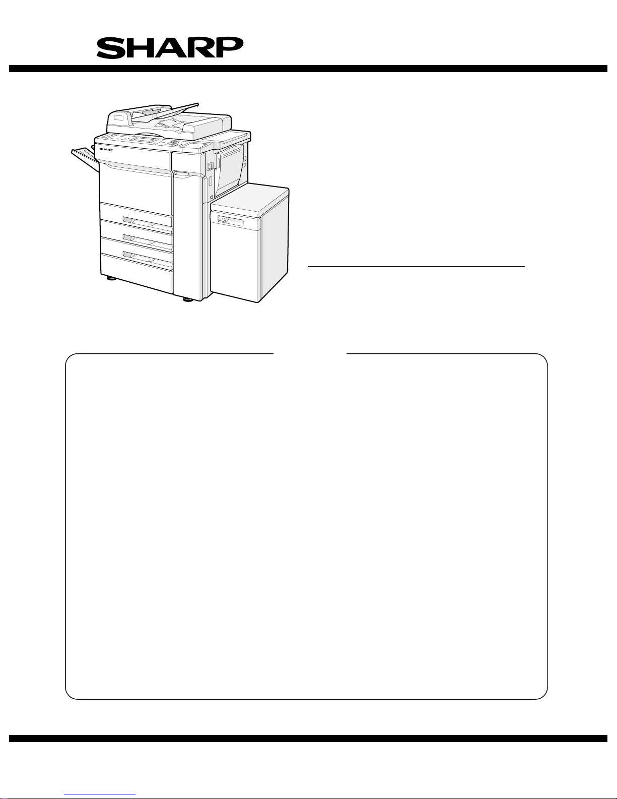
[1] GENERAL DESCRIPTION
1. The SF-2050 is a high speed copier which allows copying of 50
sheets per minute, and first copy at the at the highest speed in the
class with remarkable copying efficiency.
2. Target users
Average copy volume: 20,000 ∼ 25,00 0 sh ee t s
Scope: 10,000 ∼ 60,000 sheet s
3. Characteristics of the product
(1) Improvements in the basic functions
• First copy: 2.7 sec
• Automatic duplex function (standard)
• Large capacity tray (3 trays + LCC), max. 4,550 sheets
(5,500 sheets in Japan)
Improved efficiency in duplex copy (Single → duplex efficiency 75%)
• RADF and the staple sorter are optionally available to pro-
vide higher copy productivity.
(2) High copy volume
• Console design
• AICS (Active Image Control System) provided.
• Non-stop/non-slow-down copy (Japan)
• Toner supply during copying
• Paper supply to a non-active tray during copying
(3) Measures against environmental problems
• Low noise (Conforming to Blue Angel standards.)
• Low ozone 0.02mg/m or less
• Low power consumption, 15% down from the conventional
model (SF-9400)
(4) Improved manipulation
• Front access structure
• LCD display
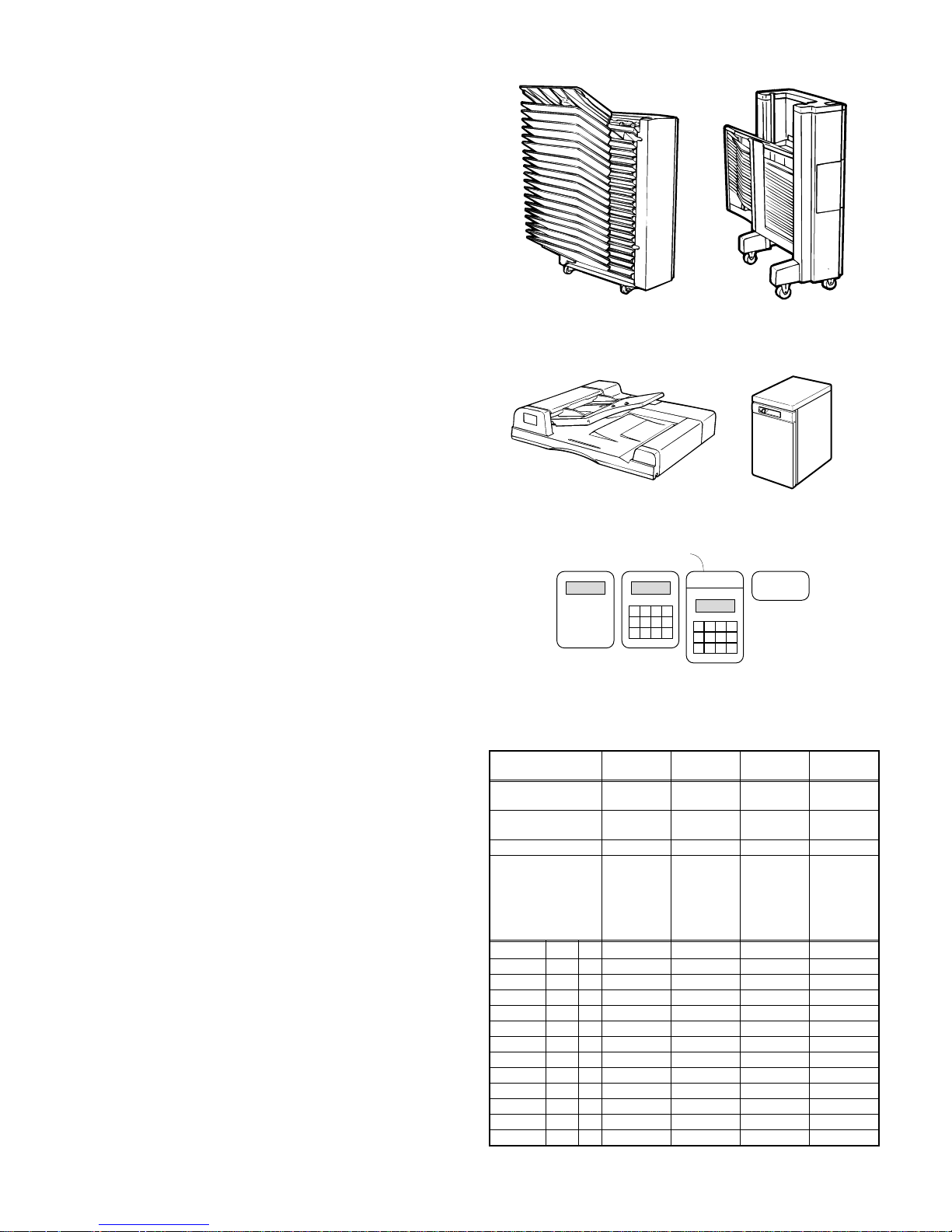
(5) Options
• RADF: SF-A55 (New)
• 20-bin sorter: SF-S16 (Used in the SD-2060)
• 20-bin staple sorter: SF-S53 (Used in the SD-2060/SF-
2035)
• Large capacity tray
(LCC):
• Card type counter: SF-EA11 (Used in the SD-2060/SF-
• Password type
counter:
• Personal counter: SF-71A/B
SF-C52 (New)
2035)
SF-EA12 (Used in the SD-2060/SF-
2035)
20-b in sort er
(SF-S16)
Duplex reversing automatic
document feeder
(SF-A55)
Card type department control counter (SF-EA11)
Password type department control counter (SF-EA12)
Commander (SF-EA13)
Personal counter (SF-71A/B)
SD-2050
Japan
No. of paper feed tray
steps
Platen original size
detection
RADF Option Standard Option Standard
LCC Option (3,300)
Destination
Japan
SEC AU
SECL AL
SEEG GG
SEEG BG
SUK BK
SCA BA
SCNZ BE
SRS BE
SRH BE
STCL BE
Agent AE
Agent BE
4 trays (550) 3 trays (500) 3 trays (500) 3 trays (500)
SF-2050
Standard
(Shipped
separately
from the
20-bin staple sorter
(SF-S53)
Large capacity tray
(SF-C52)
US
✕✕✕
(3,000)
body)
SF-2050
EX1
Option (3,000) Option (3,000)
SF-2050
EX2
1 – 1
Page 7
[2] PRODUCT SPECIFICATIONS
1. Basic specifications
(1) Type: Console
(2) Copying system: Dry, electrostatic transfer system
(3) Original Kinds: Sheet, book, cubic
Max. original size A3, 11 × 17
Original reference position Center left
Detection Japan, YES; outside Japan, NO
Detection size A3, B4, A4, A4R, B5, B5R
Option
Original load capacity 50 sheets
Original size A3 ∼ A5, 11 × 17 ∼ 5.5 × 8.5
Original replacement
speed
Original weight
(Excluding special
paper)
Mixed original feed Possible
(4) Copying speed
A3 28 28 27
B4 32 30 31
A4 (Portrait) 50 43 36
A4 (Landscape) 39 37 36
B5 (Portrait) 50 48 36
B5 (Landscape) 39 37 36
11 × 17 28 28 27
8.5 × 14 32 30 31
8.5 × 11 (Portrait) 50 43 36
8.5 × 11 (Landscape) 39 37 36
(Note) The speeds at enlargement/reduction are at the mag-
nification ratio of the lowest speed.
(5) First copy time about 2.7sec (paper feed port: tray 1)
First copy time at each paper feed port (sec)
Paper feed
port
Tray 1 2.7
Tray 2 2.9 Manual feed 2.9
Tray 3 3.1 LCC 2.8
(6) Warm-up time
Japan About 4 min
Outside Japan About 3 min
Pre-heat
Jam recovery
time
(7) Multi copy: max. 999 sheets
RADF (Standard except for
Japan/SEEG/SUK)
50 sheets/min (A4, 8.5 × 11)
Signal
mode
Duplex
mode
Normal
First copy
time
(Japan) 35 ∼ 128 g/cm
(Outside Japan) 50 ∼
128 g/cm
2
(Japan) 50 ∼ 110 g/cm
(Outside Japan) 50 ∼
110 g/cm
2
Reduction
(50%)
Paper feed
port
Tray 4
(Japan only)
YES (Selected by the key operator
program (P31).)
4 sec or less (Jam outside the fusing
section)
Enlargement
First copy
(200%)
time
3.3
(8) Copy magnification ratio
Fixed
magnification
ratio
AB series: 4R+4E: 200, 141, 122, 115,
100, 86, 81, 70, 50 %
Inch series:4R+4E: 200, 141, 129, 121,
100, 95, 77, 64, 50 %
Zoom range 50 ∼ 200% (151 steps in 1% increm ent)
(9) Exposure
(9)-1 Exposure system: Slit exposure by moving the optical
system (Fixed original table)
(9)-2 Exposure mode: Auto/Manual/Photo
(9)-3 Manual steps: 9 steps (Manual/Photo)
(10) Paper feed
(10)-1 Paper feed system: (Japan) 4 trays + multi manual feed
(Outside Japan) 3 trays + multi
manual feed
(For SEC/SECL, LCC is a standard
provision.)
(10)-2 Paper feed
capacity:
2
(10)-3 Details of the paper feed section
(Japan) 550 × 4 + 50
(Outside Japan) 500 × 3 + 50
AB series
2
Paper feed
Tray 2
Tray 1
Tray 3
Tray 4
(Japan only)
port
Paper feed
capacity
500 sheets
(500 sheet
in Japan)
500 sheets
(550
sheets in
Japan)
Paper size
A4, A4R,
B5, B5R,
B4, A3,
(*A5)
A4, A4R,
B5, B5R,
B4, A3
Paper
weight
52 ∼
80g/m
14-21 lbs
52 ∼ 80
2
, 14 ∼
g/m
21 lbs
2
,
Size
selection
Guide
change is
made by a
serviceman.
Guide
change is
made by a
serviceman.
Side/front
Front/
drawer
integrated
Frontdrawer
integrated
Inch series
Paper feed
Tray 2 500 sheets
Tray 1
Tray 3
port
Paper feed
capacity
500 sheets
Paper size
8.5 × 11
8.5 × 11R
8.5 × 14
11 × 17
(*8.5 × 5.5)
8.5 × 11
8.5 × 11R
8.5 × 14
11 × 17
Paper
weight
52-80g/m
14-21 lbs
52-80g/m
14-21 lbs
Guide
2
change is
made by a
serviceman.
Guide
2
change is
made by a
serviceman.
Size
selection
Side/front
Front/
drawer
integrated
Front/
drawer
integrated
* For A5 (8.5" × 5.5"), the rear edge guide is required.
8.8" × 13" is feedable.
Manual feed section
Paper size
AB series: A3 ∼ A6R
Inch series: 11 × 17 ∼ 5.5 × 8.5
Multi paper feed: 56 ∼ 80 g/m2,
15 ∼ 21 lbs
Single paper feed:52 ∼ 128 g/m2,
Paper weight
15 ∼ 21 lbs
(When exceeding
104 g/m2,
A4 or smaller.)
Paper kinds
Standard paper, specified paper, special
paper, OHP film, Postcard, etc,
(Japan) A3, A4, A4R, B4, B5, B5R
(Outside Japan AB series)
Detection size
(Outside Japan inch series)
A3, B4, A4, A4R, A5
11 × 17, 8.5 × 12, 8.5 × 11,
8.5 × 11R, 8.5 × 5.5
2 – 1
Page 8
(11) Developing system: Dry, two-component magnetic brush
development
(12) Charging system: (–) DC saw teeth electrode system
(13) Transfer system: (–) DC corotron system
(14) Separation system: (–) AC corotron system
(15) Fusing system: Heat roller system
(16) Cleaning system: Counter blade system
(17) Light source: Halogen lamp
(18) Void width
Void area Lead edge: 3mm or less
BAck surface void area Rear edge: about 3mm
Image loss Normal: 4mm or less
(19) Automatic duplex
Standard
Japan: A3, A4, A4R, B4, B5, B5R
Outside Japan AB series:
Size
Outside Japan inch series:
A3, A4, A4R, B4, B5
11 × 17, 8,5 × 14, 8.5 ×
11, 8.5 × 11R
Capacity 50 sheets (all sizes)
Paper weight 56 ∼ 80 g/m
2
(20) Paper exit/finishing
Paper exit tray capacity 250 sheets
Finishing
Option
20-bin sorter, 20-bin staple sorter
(21) Additional functions
Name Function Content
Automatic paper
selection (APS)
Japan: Yes
Outside Japan: Only with RADF
Japan: Yes
Automatic
magnification
selection (AMS)
Outside Japan: Only with RADF
During used of RADF,
AMS by scanning in
impossible. (PAT
prevention)
Shift copy YES
Shift width 9mm, 1/4 inch
(adjustable)
Dual page copy YES Enlargement is impossible.
Edge erase YES
Edge erase/center
erase/edge and center erase
Center erase YES
Cover copy YES
Covers/back covers/front and
rear covers
Inserts copy YES
OHP inserts copy YES
Job memory YES 9 kinds
Auditor YES 50 departments
Key operator
program
Communication
features
YES
YES
Bi-directional (The I/F PWB is
a service parts.)
Process control YES
For SUK, toner save mode is
Toner save mode YES
not available. For Japan,
serviceman mode selection.
Auto tray
switching
Installed tray
priority selection
Pre-heating YES
YES
YES (PAT. prevention)
Switching by key operator
program
(22) Power source Voltage: 100V, 110V, 120V, 127V,
200V, 220V, 220 ∼ 230V,
240V
Frequency: 50/60 Hz common
(23) Power consumption Max. power consumption:
Japan, 1500W (with options);
Outside Japan, 1920W (with options)
(24) External view W × D × H (mm)
750 × 660 × 950 (Glass top)
750 × 660 × 995 (OC cover top)
750 × 660 × 1137 (RADF top)
Occupying area W × D (mm)
1407 × 660 (with the paper exit tray,
when the manual feed is open.)
Weight:
131 kg (Body only)
145 kg (with RADF)
(25) Accessories
Packed with the main body (supply parts only)
OPC drum (installed to the body) × 1
Developer (1.0kg) × 1
Toner cartridge (0.93kg) × 1
Upper/lower heat roller (installed to the body) each × 1
Upper/lower fusing separation pawl (installed
to the body)
Upper/lower cleaning roller (lower cleaning
roller: installed to the body)
each × 1
each × 1
Cleaner blade (installed to the body) × 1
Waste toner bottle (installed to the body) × 1
2 – 2
Page 9

2. Supply parts
1 SEC
No. Name Content Life Product name Packing
1 Drum OPC drum × 1 200K SF-250DR 10
2 Developer (Black) Developer (1.0kg) × 10 100K × 10 SD-360MD 1
3 Toner (Black) Toner cartridge (0.93kg) × 10 28K × 10 SD-360MT 1
4 Upper heat roller kit Upper heat roller × 1
Fusing separation pawl (Upper) × 4
Fusing gear × 1
5 Lower heat roller kit Lower heat roller × 1
Fusing separation pawl (Lower) × 4
6 Cleaner blade Cleaner blade × 10 100K × 10 SD-360CB 1
7 Upper cleaning roller Upper cleaning roller × 10 100K × 10 SF-250UR 1
8 Lower cleaning roller Lower cleaning roller × 10 100K × 10 SF-250LR 1
9 Waster toner bottle Waste toner bottle × 1 100K SF-250TB 5
10 200K maintenance kit SF-250CP × 5
(Drum separation pawl × 2)
(Charging plate unit × 1)
(CL side seal F/R × 1)
(DV side seal F/R × 1)
(Toner reception seal × 1)
11 Staple cartridge Staple cartridge × 5 5000 × 5 SD-LS20 10
The screen grid (200K), the charger wire (200K), the ozone filter (400K), and the toner reception seal (200K) are service parts.
The waste toner bottle (100K), and charging plate unit (200K), and the DV seal (400K) are also available as service parts.
* The developer is in common with the SD-2060/3062. This model uses one bag (100K).
2 SECL
No. Name Content Life Product name Packing
1 Drum OPC drum × 1 200K SF-250DR 10
2 Developer (Black) Developer (1.0kg) × 10 100K × 10 SD-360MD 1
3 Toner (Black) Toner cartridge (0.93kg) × 10 28K × 10 SD-360MT 1
4 Upper heat roller kit Upper heat roller × 1
Fusing separation pawl (Upper) × 4
Fusing gear × 1
5 Lower heat roller kit Lower heat roller × 1
Fusing separation pawl (Lower) × 4
6 100K PM kit Cleaner blade × 1
Waste toner bottle × 1
Upper cleaning roller × 1
Lower cleaning roller × 1
7 200K PM kit Drum separation pawl × 2
Charging plate unit × 1
Screen grid × 1
CL side seal F/R × 1
DV side seal F/R × 1
Toner reception seal × 1
8 Staple cartridge Staple cartridge × 5 5000 × 5 SD-LS20 10
* The developer is in common with the SD-2060/3062. This model uses one bag (100K).
400K SF-250UH 5
200K SF-250LH 5
200K SF-250CK 1
400K SF-250UH 5
200K SF-250LH 5
100K SF-250KA 1
200K SF-250KB 5
2 – 3
Page 10

3 SEEG/SUK
No. Name Content Life Product name Packing
1 Drum OPC drum × 1 200K SF-250DM 10
2 Developer (Black) Developer (1.0kg) × 10 100K × 10 SD-360LD 1
3 Toner (Black) Toner cartridge (0.93kg) × 10 28K × 10 SD-360LT 1
4 Upper heat roller kit Upper heat roller × 1
5 Lower heat roller kit Lower heat roller × 1
6 100K PM kit Cleaner blade × 1
7 200K PM kit Drum separation pawl × 2
8 Staple cartridge Staple cartridge × 5 5000 × 5 SD-LS20 10
* The developer is in common with the SD-2060/3062. This model uses one bag (100K).
Fusing separation pawl (Upper) × 4
Fusing gear × 1
Fusing separation pawl (Lower) × 4
Waste toner bottle × 1
Upper cleaning roller × 1
Lower cleaning roller × 1
Charging plate unit × 1
Screen grid × 1
CL side seal F/R × 1
DV side seal F/R × 1
Toner reception seal × 1
400K SF-250UH 5
200K SF-250LH 5
100K SF-250KA 1
200K SF-250KB 5
4 Asia, Middle/South America
No. Name Content Life Product name Packing
1 Drum OPC drum × 1 200K SF-250DR 10
2 Developer (Black) Developer (1.0kg) × 10 100K × 10 SD-360CD 1
3 Toner (Black) Toner cartridge (0.93kg) × 10 28K × 10 SD-360CT 1
4 Upper heat roller kit Upper heat roller × 1
Fusing separation pawl (Upper) × 4
Fusing gear × 1
5 Lower heat roller kit Lower heat roller × 1
Fusing separation pawl (Lower) × 4
6 100K PM kit Cleaner blade × 1
Waste toner bottle × 1
Upper cleaning roller × 1
Lower cleaning roller × 1
7 200K PM kit Drum separation pawl × 2
Charging plate unit × 1
Screen grid × 1
CL side seal F/R × 1
DV side seal F/R × 1
Toner reception seal × 1
8 Staple cartridge Staple cartridge × 5 5000 × 5 SD-LS20 10
* The developer is in common with the SD-2060/3062. This model uses one bag (100K).
400K SF-250UH 5
200K SF-250LH 5
100K SF-250KA 1
200K SF-250KB 5
2 – 4
Page 11
5 SCA, SCNZ, Middle East, Africa
No. Name Content Life Product name Packing
1 Drum OPC drum × 1 200K SF-250DM 10
2 Developer (Black) Developer (1.0kg) × 10 100K × 10 SD-360LD 1
3 Toner (Black) Toner cartridge (0.93kg) × 10 28K × 10 SD-360LT 1
4 Upper heat roller kit Upper heat roller × 1
5 Lower heat roller kit Lower heat roller × 1
6 100K PM kit Cleaner blade × 1
7 200K PM kit Drum separation pawl × 2
8 Staple cartridge Staple cartridge × 5 5000 × 5 SD-LS20 10
* The developer is in common with the SD-2060/3062. This model uses one bag (100K).
Fusing separation pawl (Upper) × 4
Fusing gear × 1
Fusing separation pawl (Lower) × 4
Waste toner bottle × 1
Upper cleaning roller × 1
Lower cleaning roller × 1
Charging plate unit × 1
Screen grid × 1
CL side seal F/R × 1
DV side seal F/R × 1
Toner reception seal × 1
400K SF-250UH 5
200K SF-250LH 5
100K SF-250KA 1
200K SF-250KB 5
3. Environmental conditions
The following environmental conditions should be preserved for assuring copy quality and proper machine operations.
1 Standard conditions
Temperature, 20 ∼ 25 C; humidity, 65 ±5% RH
2 Operational conditions
Humidity (RH)
3 Transit conditions
Humidity (RH)
4 Supply store conditions
Humidity (RH)
2 – 5
Page 12
[3] OPTION SPECIFICATIONS
1. SF-A55
Name Duplex reversing automatic document feeder
Document feed system Continuous, automatic feed
Document exit system Face up exit
Document transport system One-belt, (center reference)
Document set direction Face up
Document size A3 ∼ B5
Document weight Thin paper mode, 35 ∼ 50g/m2;
Document set quantity Max. 50 sheets (35 ∼ 80g/m2)
Functions Document reversing (Duplex documents), SDF/ADF mode
Power source Supplied from the copier body.
Dimensions 595mm (W) × 525mm (D) × 130mm (H) (without tray)
Weight About 150 kg
2. SF-S16
Name 20-bin sorter
No. of bins 20 bins
Storing system Copy face up
Storing capacity of each bin Max. 50 sheets (Top bin, 100 sheet) Collatable paper
Power source Supplied from the copier body.
Dimensions 550mm (W) × 519mm (D) × 924m (H)
Weight About 26.5kg
standard mode, 51 ∼ 128g/ m
(Max. 30 for A3 and 11" × 17")
selection, mixed paper feed, random paper feed
size/weight
2
3. SF-S53
4. SF-C52
Name Staple sorter
No. of bins 21 bins
Storing system Face up
Storing capacity of each bin Max. 50 sheets (Top bin, 250 sheet) Collatable paper
size/weight
No. of sheets staplable 50 sheets (80g/m2 paper)
Power source Supplied from the copier body.
Dimensions 475mm (W) × 597mm (D) × 995mm (H)
Weight About 42.1kg
Name Large capacity cassette (LCC)
Paper feed capacity 3,000 sheets
Paper feed size A4/B5
Paper weight 52 ∼ 80g/m
Power source Supplied from the copier body.
Dimensions 294mm (W) × 536mm (D) × 523mm (H)
Weight 26kg
2
3 – 1
Page 13

[4] PAPER
1. Standard paper for tray feed
Name Size Type
A3 SF-3AS2 250 sheets
B4 SF-4BS2 500 sheets
Standard type
General type
paper (thick)
Thick paper
Recycled
paper
Color paper
A4 SF-4AS2 500 sheets
SF-5BS2 (Horizontal)
B5
SF-5Bs3 (Vertical)
A5* SF-5AS2 250 sheets
B6* SF-6BS2 250 sheets
A3 SF-3AM2 250 sheets
B4 SF-4BM3 500 sheets
SF-4AM2 (Horizontal)
A4
SF-4AM3 (Vertical)
SF-5BM2 (Horizontal)
B5
SF-5BM3 (Vertical)
A3 SF-3AH
B4 SF-4BH
A4 SF-4AH
B5 SF-5BH
A3 SF-3AR1
B4 SF-4BR1
A4 SF-4AR1
B5 SF-5BR1
SF-4B1R (Pink)
B4
SF-4B1B (Blue)
SF-4B1G (Green)
SF-4A1R (Pink)
SF-4A1Y (Cream)
A4
SF-4A1B (Blue)
SF-4A1G (Green)
SF-5B1R (Pink)
SF-5B1Y (Cream)
B5
SF-5B1B (Blue)
SF-5B1G (Green)
Quanty in one
bag
500 sheets
each
500 sheets
each
500 sheets
each
250 sheets
each
500 sheets
each
500 sheets
each
500 sheets
each
500 sheets
each
● <Note> ● - - - - - - - - - - - - - - - - - - - - - - - - - - - - - - - - - - - - - - -
• Be sure to use the above paper on the tray. For the paper with
mark "*," use in the manual feed mode.
- - - - - - - - - - - - - - - - - - - - - - - - - - - - - - - - - - - - - - - - - - - - - - - - - ●
2. Special paper (Manual feed only)
Name Size Type
Postcards A4 SF-4A5C 100 sheets
Second original
paper
Label paper A4 SF-4A3F 100 sheets
OHP film A4 SF-4A6F 100 sheets
B4 SF-4B2A
A4 SF-4A2A
No. of sheets in one
bag
500 sheets each
4 – 1
Page 14
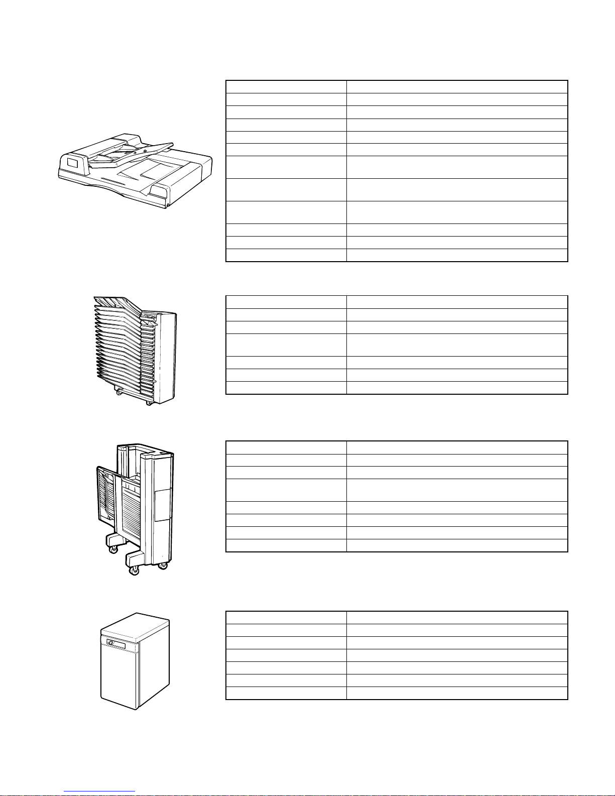
[5] PRODUCT VIEW
1. External view
1011 7
12
1 8
2. Internal view
6 2
9
6
15
3
4
5
7
3
13
Operation panel
1
Manual feed guide
3
Manual feed tray
5
Original cover
7
Original table
9
Contrast adjusting knob
G
Tray
I
Power switch
K
142
Front cover
2
Manual feed additional tray
4
Toner cover
6
Original stocker
8
Clip tray
F
Copy tray
H
Paper feed pressure
J
release button
Roller rotation knob
1
Transport section
3
open/close lever
Waste toner box
5
OPC drum
7
Transport section
2
adjustment knob
Duplex tray
4
Fusing section
6
54 1
5 – 1
Page 15
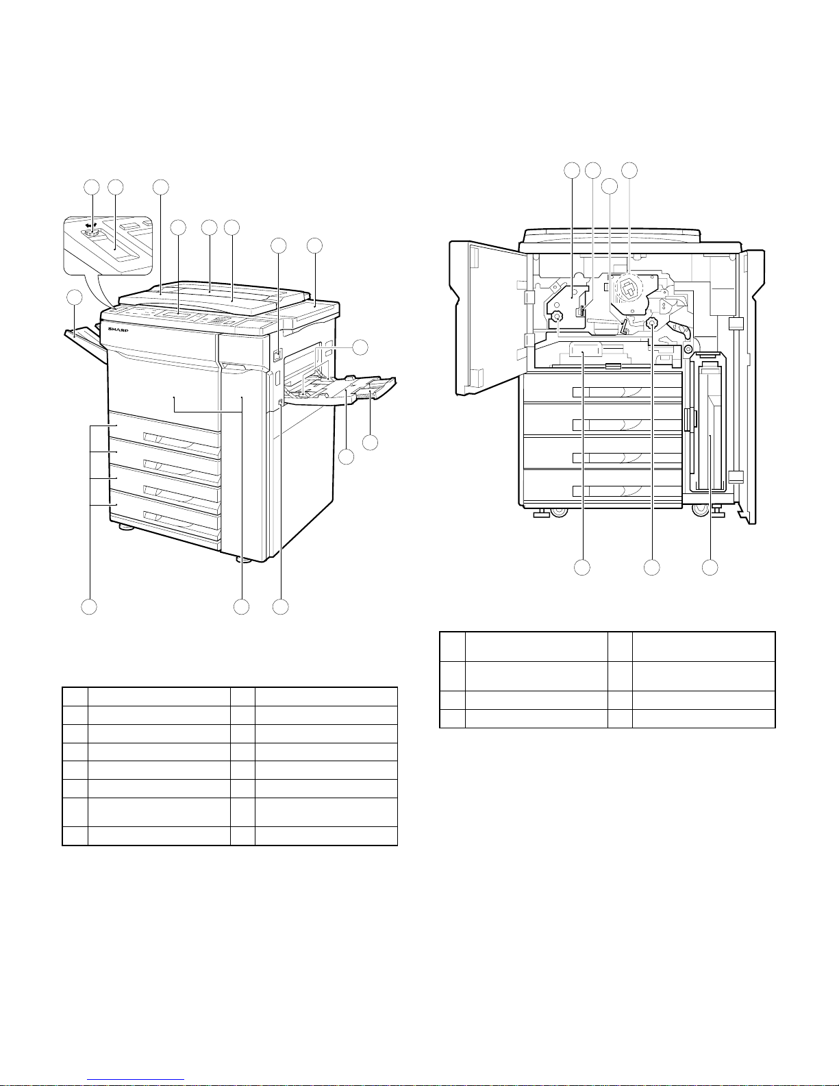
3. Operation panel
1
2
3
4
5
6 7
13 141516
TRAN SPARENCY
INSERTS
SHFT
INSERT S
SORTER ORIGINAL TO COPY
SORT
ATAPLE
SORT
GROUP
MARGIN
COVERS/
89
Contrast adjustment knob
1
Edge erase key/display lamp
5
Duplex key/display lamp
9
Message forward scroll key
I
Tray selection key
M
Clear (C) key
Q
ERASE
1 12
(ORIGINALS)
EVEN NUMBER
ODD NUMBER
2
11
2
PRE-COUNT
ORIGINALS
DUAL PAGE
COPY
2
AUTO IMAGE
REDUCTION
ENLARGEMENT
100%
ZOOM
EXPOSURE
ARTO
MANUAL
DARK
LIGHT
PHOTO
11 17
12
OHP insert paper insertion
2
key/display lamp
Dual paper copy key/display
6
lamp
Zoom key
F
Operation guide key/display
J
lamp
Interruption key/display lamp
N
Start key/Start lamp
R
2410
SCROLL DISPLAY
INFORMATION
TRAY SELECT
PROGRAM
P
CLEAR ALL
CA
INTERRUPT
1
4
7
AUDIT CLEAR
18 19 20 21 22 23
Cover/insert paper insertion
3
key/display lamp
Automatic magnification ratio
7
selection key/display lamp
Copy density key
G
Program key
K
Numeric key
O
Copy quantity display
S
32
START
65
98
0/
C
Shift key/display lamp
4
Sort key/display lamp
8
Reduction
H
All clear key
L
Zero/department count end
P
key
Message screen
T
5 – 2
Page 16
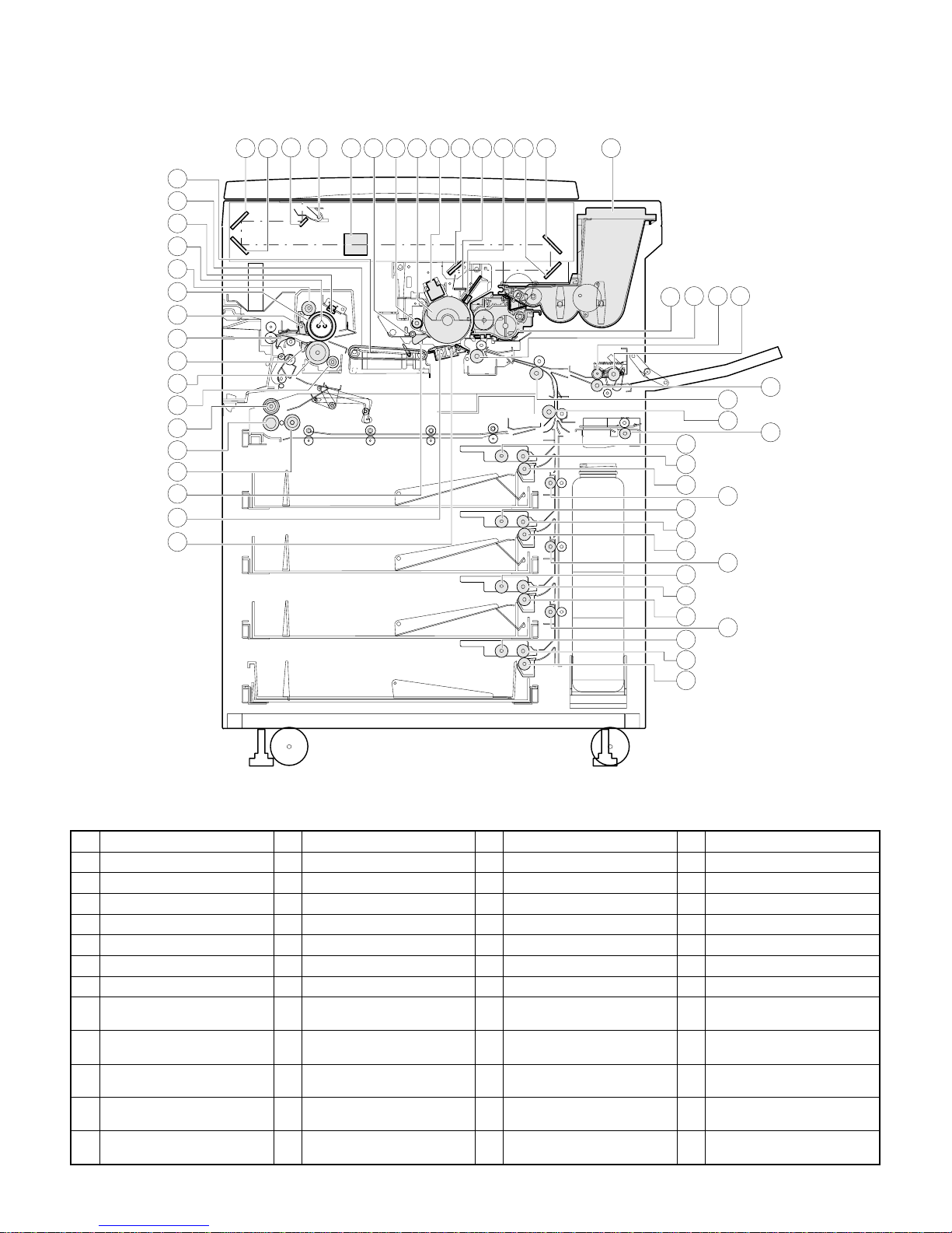
4. Internal structure (Japan model)
19
20
27
23
26
21
25
28
24
22
48
49
50
51
46
16
14
3
2
1
468710911
15
18
175
47
12
34
35
36
37
38
39
40
41
42
43
44
45
32
30
13
32
32
32
32
29
31
33
No. 2 mirror
1
Lens unit
5
No. 4 mirror
9
Transport roller (upper)
I
Drum separation pawl
M
Upper heat roller
Q
Upper separation pawl
U
manual take-up roller
Y
Large cassette tray unit paper
]
feed roller
No. 2 tray take-up roller
a
No. 3 tray paper feed roller
e
No. 4 tray paper feed reverse
i
roller
Duplex section paper feed
m
roller
No. 3 mirror
2
Main charger unit
6
No. 5 mirror
F
Transfer charger
J
Cleaner unit
N
Lower heat roller
R
Upper cleaning roller
V
Manual paper feed roller
Z
No. 1 tray take-up roller
^
No. 2 tray paper feed roller
b
No. 3 tray paper feed reverse
f
roller
Process control sensor
j
Duplex section paper feed
n
reverse roller
No. 1 mirror
3
Blank lamp
7
Developing unit toner box
G
Photoconductor drum
K
Suction unit
O
Heater lamp
S
Fusing thermistor
W
Manual separation roller
[
No. 1 tray paper feed roller
_
No. 2 tray paper feed reverse
c
roller
No. 4 tray take-up roller
g
Drum marking sensor
k
Duplex section take-up roller
o
5 – 3
Copy lamp
4
No. 6 mirror
8
Developing unit
H
Separation charger
L
Suction belt
P
Lower separation pawl
T
Paper exit separation gate
X
Resist roller
\
No. 1 tray paper feed reverse
‘
roller
No. 3 tray take-up roller
d
No. 4 tray paper feed roller
h
Lower cleaning roller
l
Page 17
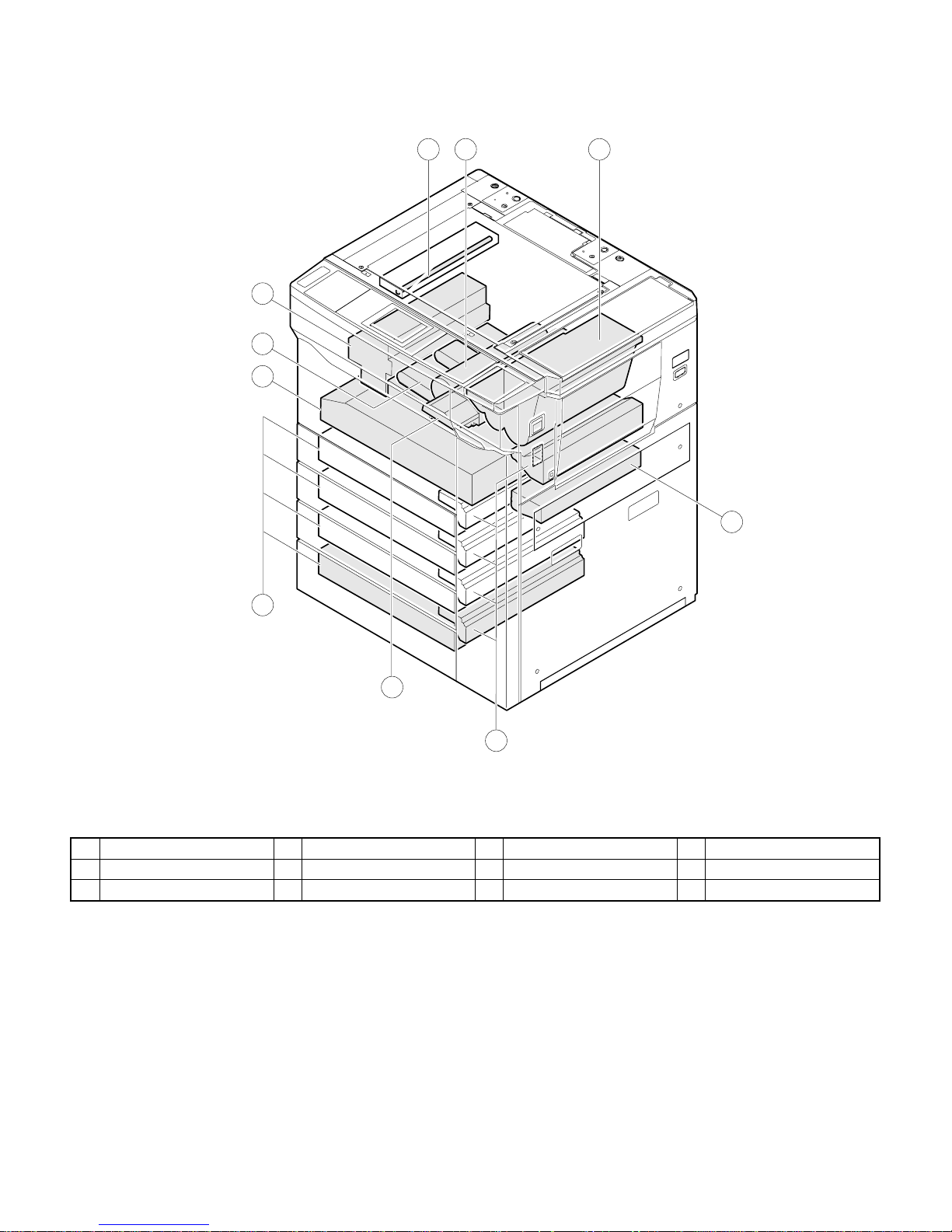
5. Unit
4
1
3
2
6
8
7
Process unit
1
Developing unit
5
500-sheet tray unit
9
9
5
10
Suction frame unit
2
Toner hopper unit
6
Paper feed unit
F
Fusing unit
3
Transport unit
7
Optical unit
4
Center tray unit (ADU)
8
5 – 4
Page 18
6. Clutches and solenoids
1619 21 913 1517 20
11
12
10
Signal name Part name Function and operation Remark
CPFC1 No. 1 cassette paper feed clutch No. 1 tray paper feed roller rotation
1
CPFS1 No. 1 cassette paper feed solenoid No. 1 tray take-up roller rotation
2
CPFC2 No. 2 cassette paper feed clutch No. 2 tray paper feed roller rotation
3
CPFS2 No. 2 cassette paper feed solenoid No. 2 tray take-up roller rotation
4
CPFC3 No. 3 cassette paper feed clutch No. 3 tray paper feed roller rotation
5
CPFS3 No. 3 cassette paper feed solenoid No. 3 tray take-up roller rotation
6
CPFC4 No. 4 cassette paper feed clutch No. 4 tray paper feed roller rotation Japan only
7
CPFS4 No. 4 cassette paper feed solenoid No. 4 tray take-up roller rotation Japan only
8
MPFS Manual feed solenoid Manual feed take-up roller pressing
9
DPFWS DP paper feed weight plate solenoid Duplex paper holding plate driving
F
DPFC Duplex paper feed clutch Duplex paper feed roller rotation
G
DTRC Duplex paper transport clutch Duplex paper transport roller rotation
H
PSPS Separation solenoid Paper separation solenoid driving
I
TRC3 Paper entry roller clutch
J
RRC Resist roller clutch Resist roller driving
K
CURLRC Curl correction clutch Curl correction section driving
L
HRS Heat roller solenoid Heat roller pressing
M
TRC1 Transport clutch 1 Transport roller rotation
N
DGS Duplex gate solenoid Duplex gate ON/OFF
O
TRC2H Transport clutch 2 (High speed) Transport roller rotation
P
TRC2L Transport clutch 2 (Low speed) Transport roller rotation
Q
Paper entry roller driving from large capacity tray
(LCC)
14
1
2
18
3
4
5
6
7
8
5 – 5
Page 19

7. Switches and sensors
14
25
26
16
19
22
18
20
40
43 37 36
46
34
12 1315 2829 27
35
24
45
42
17
21
44
11
9 10
41
23
30
1
2
31
3
4
32
5
6
33
7
8
38
39
Signal name Part name Switch/sensor Function/operation Remark
LUD1 No. 1 cassette upper limit sensor Sensor No. 1 tray upper limit sensing
1
PED1 No. cassette paper sensor Sensor No. 1 tray paper presence sensing
2
LUD2 No. 2 cassette upper limit sensor Sensor No. 2 tray upper limit sensing
3
PED2 No. 2 cassette paper sensor Sensor No. 2 tray paper presence sensing
4
LUD3 No. 3 cassette upper limit sensor Sensor No. 3 tray paper upper limit sensing
5
PED3 No. 3 cassette paper sensor Sensor No. 3 tray paper presence sensing
6
LUD4 No. 4 cassette upper limit sensor Sensor No. 4 tray upper limit sensing Japan only
7
PED4 No. 4 cassette paper sensor Sensor No. 4 tray paper presence sensing Japan only
8
PLS1 Manual feed paper length sensor 1 Sensor Manual feed tray paper length sensing
9
PLS2 Manual feed paper length sensor 2 Sensor Manual feed tray paper length sensing Inch series
F
MPED Manual feed paper sensor Sensor Manual feed tray paper presence sensing
G
OCSW OC cover open/close sensor Sensor OC cover open/close sensing Japan only
H
MBHP Mirror base home position sensor Sensor No. 4, 5 mirror home position sensing
I
MHP Mirror home position sensor Sensor
J
Mirror base (No. 2, 3 mirror) home position
sensing
5 – 6
Page 20

Signal name Part name Switch/sensor Function/operation Remark
LHP Lens home position sensor Sensor Lens home position sensing
K
DPFD ADU paper feed sensor Sensor Duplex section paper feed sensing
L
DTBHPS ADU rear plate home position Sensor
M
DTWHPS ADU alignment plate home position Sensor
N
DPPD1 ADU transport sensor 1 Sensor Duplex section transport sensing
O
DPPD2 ADU transport sensor 2 Sensor Duplex section transport sensing
P
DPPD3 ADU transport sensor 3 Sensor Duplex section transport sensing
Q
DTPD ADU paper sensor Sensor Duplex section paper presence sensing
R
DFDL2 Paper feed sensor 5 Sensor LCC paper feed sensing
S
PPD3 Transport sensor 3 Sensor Paper transport sensing
T
DPID1 ADU paper entry sensor 1 Sensor Duplex section paper entry sensing
U
DPID2 ADU paper entry sensor 2 Sensor Duplex section paper entry sensing
V
TES Toner empty sensor Sensor Toner hopper toner empty sensing
W
TNCTR in Toner cartridge sensor Switch Refill toner cartridge installation sensing
X
TCS Toner density sensor Sensor Developing unit toner density sensing
Y
PFD1 Paper feed sensor 1 Sensor No. 1 tray paper feed sensing
Z
PFD2 Paper feed sensor 2 Sensor No. 2 tray paper feed sensing
[
PFD3 Paper feed sensor 3 Sensor No. 3 tray paper feed sensing
\
PFD4 Paper feed sensor 4 Sensor No. 4 tray paper feed sensing Japan only
]
DSWF1 Front cover switch 1 Switch Front cover open/close sensing 100V system
^
DSWF2 Front cover switch 2 Switch Front cover open/close sensing 100V system
_
TS Thermostat — —
‘
THS Fusing temperature sensor Thermister Fusing section temperature sensing
a
TBBOX Waste toner bottle sensor Sensor Waste toner bottle presence sensing
b
TNF Waste toner full sensor Sensor Waste toner full sensing
c
DSWE Paper exit section open switch Switch Paper exit section open/close sensing 100V system
d
PPD1 Transport sensor 1 Sensor Paper transport sensing
e
PPD2 Transport sensor 2 Sensor Paper transport sensing
f
POD Paper exit sensor Sensor Paper transport sensing
g
DHSW Dehumidifier heater switch Switch Dehumidifier heater ON/OFF Japan only
h
MSW Power switch Switch Power switch ON/OFF Japan only
i
PSD Separation sensor Sensor Paper separation sensing,
j
Duplex section rear plate home position
sensing
Duplex section alignment plate home
position sensing
5 – 7
Page 21

8. Motors
6
4
57
8 1112
1
9
10
3
2
13
14
15
Mirror motor
1
No. 4, 5 mirror base motor
5
Cooling fan motor
9
Suction fan motor
I
Tray lift-up motor 3
M
Main motor
2
Lens motor
6
Ventilation fan motor 1
F
DV fan motor
J
Tray lift-up motor 4
N
Drum motor
3
Duplex motor 1 (for shifting
7
the rear plate)
Ventilation fan motor 2
G
Tray lift-up motor 1
K
16
17
18
Toner motor
4
Duplex motor 2 (for shifting
8
the alignment plate)
Ventilation fan motor 3
H
Tray lift-up motor 2
L
5 – 8
Page 22

9. PWB unit list
13
17
20
6
105 7 9 8
15
16
14
11
12
2
1
19
18
DC power PWB
1
Operation control PWB
5
LCD invertor PWB
9
Sensor volume PWB
I
Light quantity correction PWB
M
High voltage PWB
2
Operation PWB 1
6
LCD unit
F
Original sensor light emitting
J
PWB (Japan only)
Lift-up motor PWB
N
AC circuit PWB
3
Operation PWB 2
7
DL PWB
G
Original sensor light receiving
K
PWB (Japan only)
Cassette paper size sensor
O
PWB
3
4
Main control PWB
4
Operation PWB 3
8
BL PWB
H
AE sensor PWB
L
Manual feed paper size
P
sensor PWB
5 – 9
Page 23

10. Large capacity cassette unit (LCC)
8
9
6
4
10
1
3 711
5
2
Signal name Part name Switch/sensor Function/operation Remark
TLMD Tray upper limit sensor Sensor Tray upper limit sensing
1
TLD Tray lower limit sensor Sensor Tray lower limit sensing
2
TUD Tray paper upper section sensor Sensor
3
TPTD Tray shift quantity sensing PT sensor Sensor Remaining paper quantity sensing
4
TCD
5
— Tray lift motor — Tray up down
6
LPFS Paper feed solenoid — Paper feed roller pressing
7
LPFC Paper feed clutch — Paper feed roller rotation
8
LPFC2 Paper feed reverse clutch — Double feed preventing clutch
9
— Fuse PWB unit — —
F
— Upper lock SW Switch
G
Door open
Tray SW PWB
— Door (tray) open/close sensing
Tray paper upper section and paper
presence sensing
Upper limit lock sensing (Cutting the motor
power for safety.)
5 – 10
Page 24

[6] PROCESS SECTION
(Photocondor drum and cleaning
unit)
Dark area Dark area
HV
CTL
Light
1. Basic theory
With the indirect static copier, a plain paper is used for the copy
paper. As a latent static image is formed on the surface of the
photoconductor, the image is then developed into visible (toned)
image using the toner. Then the toner is transferred onto the copy
paper.
The plain paper copier (PPC) has six basic processing steps of
corona charge, exposure, development, transfer, discharge, and
cleaning. The cleaning step prepares the photoconductor surface for
repeated use.
(1) Image forming process
Charging
1
Exposure
Transfer
2
3
Development
Discharge
Cleani ng
1 Corona charges the photoconductor.
2 The photoconductor is exposed to light to form a static latent
image.
3 Toner is attracted to the static latent image.
4 The toner on the drum is transferred onto the copy paper.
5 Toner remaining on the photoconductor (residual toner) is
removed.
6 The charge remaining on the photoconductor surface (residual
charge) is removed.
6
Photoconductor
5
4
(2) Photoconductor
While some materials conduct electricity, others do not. Materials,
therefore, can be put into three categories of conductor, semiconductor, and insulator.
These categories are conceptual, distinct classification is difficult.
Generally, the following is applied.
Material whose specific resistance is over 103Ωcm is called a insulator and under 10–3Ωcm is called a conductor.
Those which exist between the two normally called semiconductor.
Conductor in the category always has the electrical conductivity, while
semiconductor does not. But, it may become conductor under certain
conditions.
The photoconductor used by the copier is an insulator when not
exposed to light, but its electrical resistance abates when exposed to
light. When exposed to light, the photoconductor surface becomes
conductive. Material having the property to become conductive in
light (photo conductive phenomenon) is a photoconductor or
photosemiconductor.
CGL
Base
Theory of photoconduction
(3) Types of photoconductors
The principal materials of a photoconductor are zinc oxide (ZnO),
amorphous selenium (amorphous Se), selenium alloy, cadmium sulfide (CdS), amorphous silicon (amorphous Si), and organic photoconductor (OPC).
Amorphous selenium(amorphousSe)
Selenium alloy
Inorganic photoconductor
Organic photoconductor
Described next are structures of the photoconductors we have used
up to now.
Zinc oxide (ZnO) master
Cadmium sulfide (CdS) drum
Organic photoconductor (OPC) master and dr um
Selenium (Se) drum
Zinc oxide(ZnO)
Cadmium sulfide(CdS)
Amorphous silicon( am or phous Si)
Organi c pho toc onduc t or (O PC)
Photoconductive l ayer (zinc oxide layer)
Intermediate layer
Paper
Back coatin g pa per
PET layer
Micro space layer
Photoconductive layer (C dS layer)
Aluminum layer
Charge traffic layer
Charge generation layer
Alum i n um layer
Photoconducti ve layer
Alum i n um la y e r
(selenium layer)
Base paper
Optical
conductive
layer
(OPC layer)
6 – 1
Page 25

Zn0 OPC CdS Se
Photoconductor
sensitivity
Photoconductor
strength
Photoconductor
life
4321
4321
Several hundred
cycles
Several ten
thousand cycles
Several ten
thousand cycles
Several hundred
thousand cycles
Photoconductor characteristics
1 > 2 > 3 > 4
Characteristics of organic photoconductors
• Permits a variety of structures (drum, sheet, belt)
• Higher insulation in dark area (charge acceptability and retentivity)
• Permits a variety of molecular structure (allows a variety of
molecular design)
• Light weight
• Stable against humidity and temperature
• Safe for environment (non-pollution, unrestrained disposal)
• Not strong in anti-wear property
• Not strong against light and ozone.
(4) Characteristics of photoconductor
Mentioned next is the general characteristics important to use for the
photoconductive material.
1. Photo-sensitivity 2. Spectrum characteristics
3. Acceptor potential 4. Charge retentivity
5. Residual potential 6. Fatigue
[Photo-sensitivity]
This is dependent on the attenuation speed of the potential when the
photoconductor is exposed to light.
[Spectrum characteristics]
Wave length of the light differs by the kind of the photoconductor.
[Acceptor potential]
The resistance in the dark area of the photoconductor decreased as
the electric field increases among layers.
As the electric field is formed to a higher value as the photoconductor
is charged, the resistance in the related layer decreases and the rate
of charge retained in the photoconductor is restricted. The potential of
the photoconductor in this instance is called acceptor potential which
is an important factor to determine the potential contrast. To avoid
giving electrical distortion in the photoconductor, charge is normally
made to a level slightly lower than the acceptor potential.
[Charge retentivity]
The time that the static latent image is held by the photoconductor
depends on the speed at which the potential decreases in the dark
area. For this, measure the time that the photoconductor potential
abates to half of the starting value in the dark area. This charge
retentivity may cause a problem when the time from the exposure to
the development is long. But, it may not be a problem with the
machine where a series of operations from charge, exposure, and
development are automated and time between processes is shorter.
[Residual potential]
When the charged photoconductor is exposed to light, the potential
abruptly diminishes at first, then begins decaying relatively slowly.
The potential of the photoconductor where slow decay starts is called
residual potential. A less residual potential produces a large potential
contrast, low residual charge is preferable.
The value of the residual potential affects largely the development of
gradual tone.
[Fatigue]
If charge and exposure are repeated, the phenomenon called
photoconductor fatigue occurs. In other words, it appears as an increase of the decay speed of the photoconductor potential or a
decrease in the charge retentivity.
Now, we have learned about the characteristics required for charging
of the photoconductor. If charge is repeated from the corona unit in
the actual operation, the corona wire is likely to be contaminated with
dust, stain, and scattered toner, causing uneven corona charge. To
avoid this, the corona wire needs to be cleaned well.
1.0
0.8
0.6
0.4
0.2
Spectrum sensitivity (relative value)
400
Se:Te
OPC
500 600 700 800
Wavelength
Spectrum sensitivity
Amorphous sil ic on
Relationship between color and wave length
Light having wave length of 380nm through 780nm can be recognized by human eyes, which is called visible light. Wave length
shorter than that is called ultraviolet light and the longer than that is
called infrared light. Figure below shows the relationship between the
wave length of light and color.
Blue green
Blue
Violet
350 400 450 500 550 600 650 700 750 800
Yellow
Green
Orange
Red Inf ra re dUltraviolet
6 – 2
Page 26

2. SF-2050 basic process and
structure
• The Scorotron method is used to evenly charge the photoconduc-
tor surface to the given potential in the charge process. The
corona wire regularly used is now replaced with a new corona
charge mechanism that employs the 0.1mm thick stainless steel
saw teeth plate, in order to suppress ozone which is generated
when the oxide molecule in air is ionized.
• Considering the service efficiency, the process separation
mechanism is adopted.
(1) Details of image forming process
STEP 1. Charging
The main corona discharges negative corona to give negative charges to the OPC drum surface evenly.
The surface potential of the OPC drum is controlled by the screen
grid voltage to maintain at the potential equal to the grid voltage.
• When the drum surface voltage is lower than the screen grid volt-
age, electric charges from the main corona pass through the
screen grid to reach the drum surface and charge it until the drum
surface voltage becomes equal to the grid voltage.
• When the drum surface voltage reaches almost the same level as
the grid voltage, electric charges from the main corona flow
through the electrode of the screen grid to the high voltage unit
grid voltage output circuit, thus maintaining the drum surface voltage at the same level as the grid voltage.
Exposure
Exposure
(Copy lamp)
OPC layer
Pigment layer
Aluminum
(Drum)
Dark area
Light area
Dark area
Light area
STEP 3. Development (Bias –200V)
The electrostatic latent image on the drum surface is formed into a
visible image by the toner. This copier employs the two-component
magnetic brush development system, where a bias voltage of –200V
is applied to the carrier (MG roller) and the toner is charged positively
by friction with the rotating carrier.
Carrier
Toner
Screen grid
Main corona
output section
Grid voltage
output section
High voltage
unit
STEP 2. Exposure (Copy lamp, mirror, lens)
The optical image of an original is projected through the mirrors and
lenses onto the OPC drum surfac e b y the copy lam p . Th e r e sis t a nc e
of the OPC layer reduces in the bright area (light area on the original)
to discharge negative charge, forming an electrostatic latent image on
the drum surface.
In reduction copy, the non-image area of the image is discharged by
the BL (blank lamp) after exposure.
S
N
N
N
S
-200V
STEP 4. Transfer
The visible image on the drum surface is transferred on to the copy
paper. A negative charge of the transfer corona is applied to the rear
surface of the copy paper to transfer the toner on the drum surface to
the copy paper.
Toner
Paper guide
Copy paper
High voltage uni t
6 – 3
Page 27

STEP 5. Separation
Though the copy paper and the drum are both negatively charged
after transfer, the negative potential on the drum is higher than that
on the copy paper, generating an attraction force between the drum
and the copy paper. To remove the attraction force, AC corona is
applied to the copy paper by the separation corona to raise the
potential on the copy paper to the same level as the drum surface
potential. Resultantly the attraction force is eliminated and the copy
paper is separated from the drum. If the paper is not separated from
the drum, the separation pawl works to separate it mechanically.
Separation
pawl
Copy paper
Separation corona
output section
High voltage unit
STEP 6. Cleaning
Residual toner on the drum is collected by the cleaning blade.
Photo mode
The photo mode is provided to make clear half-tone copy of the photo
originals.
In the photo mode, the grid voltage and the copy lamp voltage are
lower than in the standard copy mode (the copy density of the black
background is lowered) to provide half tone graduations of the copy.
(Dark)
Normal copy mode
Copy density
(Light)
Gradation is increased to
provide larger expression
width of half tone.
Original density
Photo mode
(The copy density of
black background is
decreased.)
(Dark)
(2) Relationship between the OPC drum and light
The light exposed is absorbed by the charge carrier generation layer
(CGL) to generate the charge carrier and moves towards the charge
carrier transport layer (CTL). The carrier reached CTL then to neutralize the surface charge.
Cleaner blade
Residual
toner
STEP 7. Discharge
The electric resistance of the OPC layer is reduced by radiation from
the discharge lamp over the drum to remove residual charges.
Discharge lamp
Grid
CTL
CGL
6 – 4
Page 28

(3) Transition of photoconductor surface potential
Deve lop
Charge Exposure
BL
-730V
Dark area
-215V
Devel opi ng bia s v olt age
Light area
(4) Photoconductor drum sensitivity correction
In the SF-2050, fall in sensitivity due to long use of the photoconductor drum is corrected by the copy lamp light intensity to prevent
against considerable change in copy quality.
The photoconductor drum sensitivity fall correction is performed as
follows:
Transfer Separate
Residual po tentia l
Clean
DL
Cleaner
OPC drum
Develop
Change the tickness of the carrier transport layer (CTL).
By the developper.
By the cleaner blade.
(NEW) (USED)
CTL
CGL
CLV
Sim46
0
7.4h
(1)
14.8h
(2)
22.2h
(3)
(Drum sensitivity correction counter)
29.6h
(4)
CTL
CGL
37.0h
(5)
74.1h(200K)
(10)
6 – 5
Page 29

(5) Process Control function
[Summary]
The Process Control function records the density of the standard
toner image formed on the photoconductor, and maintains that standard density, thereby ensuring consistent copy quality. This is accomplished by regularly checking the image density on the photoconductor surface and compensating for any deviation from the standard
density by varying the MC grid bias voltage output. The exposure is
also corrected according to the change in the high voltage output to
stabilize the half-tone areas of the copy image.
F
2 The Process Control Sensor reads the three toner patches and
the bare drum, and uses this ratio to determine the Standard level.
(The Standard level is the reference value that must be achieved
during Process Control to ensure proper copy quality. This Standard level is preset at the factory and is a result of the value stored
in Simulation 44-4).
50V
50V
Surface
Toner
image
Surface Surface
1
Toner
image
2
Toner
image
3
Surface
R
Process density
Main control PWB
CPU dens ity judge m ent
Light quantity correction
calculation
I/O MC grid
output selection
sensor PWB
Density detection
level setting
(VR2/4)
High voltage PWB
MC grid bias
output (density
correction)
in each mode
(Light quantity
correction)
Process Control
1 Three toner patches are developed on the photoconductor surface
at three different MC grid bias voltage levels. These three patches
are developed using the Photo mode high voltage output calculated the last time Process Control was performed.
The voltage values of the three patches are:
1. Photomode voltage (This is the center value and is referred to
as Vg (P))
2. Photomode voltage +50v (Vg (P) +50v)
3. Photomode voltage -50v (Vg (P) -50v)
Bias
Drum 1/2 rotation 2/2 rotation 3/2 rotation
1
2
BV
3
1
2
PV
3
PV=Tomer patch detection output level
BV=Photoconduc t or drum ba se detectio n output level
PV
x 1024=value in Sim44-4
BV
Time
(t)
Note: The value stored in Simulation 44-4 should be Japan: 130,
EX: 100.
In the SF-2050, the absolute value of the Process Control Sensor
is not used for control calculation, but the ratio of the sensor
output from the bare drum and the sensor output from the toner
patch is used.
This will allow for correct density compensation when the reflectivity of the drum is affected by dirt or drum deterioration.
3 At this time the Standard level is referenced, and three possible
conditions will exist.
a If the Standard level falls between the three patch values:
The proper MC grid bias voltage is determined in Fig. A.
Fig A
PV
BV
Standard
lever
Vg(p)+50
Vg(p)
Vg(p)+50
Vg(p)
Vg(p)-50
MC GRID BIAS VOLTAGE
6 – 6
Vg(p)-50
Proper MC grid bias voltage
deter m in ed by process contr ol
MC GRID VOLTAGE
Page 30

b If the range of the three developed toner patches is lower than
the Standard level:
Two more toner patches are developed with the voltage
values of Vg(P)+100v and Vg(P)+150v, as shown in Fig. B.
The purpose of developing two more patches is to bring the
toner patch range up to the Standard level. If the toner patch
range is still not at the Standard level, two more toner patches
are developed with the voltage values of Vg(P)+200 and
Vg(P)+250. If still another step is required, the toner patches
are developed with the voltage values of Vg(P)+300 and
Vg(P)+350. If the Standard level is achieved during any of
these steps, the proper MC grid bias is determined, and the
toner patch process is discontinued. If the Standard level is
still not achieved after these four sets of toner patches (1 set
of 3 patches and 3 sets of 2 patches), then an F2-35 condition
will occur.
Fig B
PV
BV
Standard
lever
Step3
Step2
Step1
First 3
patches
Vg(p)-50
Vg(p)+100
Vg(p)+50
Vg(p)
Vg(p)+250
Vg(p)+200
Vg(p)+150
Proper MC grid bias voltage
determined by process control
Step1 - 3patches developed
Step2 - 2patches developed
Step3 - 2patches developed
Step4 - (Not needed in this case)
IF needed-2patches
developed
4 When the MC grid bias voltage is corrected by the Process Con-
trol Sensor, the corresponding light quantity is also calculated to
control the copy lamp output.
Process Control timing
In the SF-2050, Process Control is performed at the following
intervals:
1 When the power switch is turned on.
2 When the accumulated copy time reaches 30 minutes.
If the timer reaches 30 minutes during copying, Process Control is performed during copying.
If the timer reaches 30 minutes after copying, Process control
is performed during the next copy preliminary rotation.
3 When the Stand-by time reaches 1 hour. Process control is
performed during the next copy preliminary rotation.
4 When Simulation 46 is performed.
Drum marking
In the SF-2050, a toner patch image is formed in the same position
on the photoconductor drum surface to improve the accuracy of the
process control.
A marking is provided on the drum and the marking is sensed before
forming a toner patch image. If the marking is not sensed, the density
is extremely lowered to display "F2" trouble.
R
c If the range of the three developed toner patches is higher
MC GRID VOLTAGE
than the Standard level:
Two more toner patches are developed with the voltage
values of Vg(P)+100v and Vg(P)+150v, as shown in Fig. C.
The purpose of developing two more patches is to bring the
toner patch range down to the Standard level. If the toner
patch range is still not at the Standard level, two more toner
patches are developed with the voltage values of Vg(P)+200
and Vg(P)+250. If still another step is required, two more
toner patches are developed with the voltage values of
Vg(P)+300 and Vg(P)+350. If the Standard level is achieved
during any of these steps, the proper MC grid bias is determined, and the toner patch process is discontinued. If the
Standard level is still not achieved after these four sets of
toner patches (1 set of 3 patches and 3 sets of 2 patches),
then an F2-35 condition will occur.
Fig C
PV
BV
Standar d
lever
Step1
Step2
Step3
Vg(p)-250
First 3
patches
Vg(p)-100
Vg(p)-150
Vg(p)-200
Proper MC grid bias voltage
deter m in ed by process contr ol
MC GRID VOLTAGE
Vg(p)
Vg(p)-50
Vg(p)+50
Step1 - 3patches developed
Step2 - 2patches developed
Step3 - 2patches developed
Step4 - (Not needed in this case)
IF needed-2patches
developed
F
3. Basic structur e
Photoconductor drum: The 80mm ground plate of the OPC drum
is on the rear frame side of the drum unit
so that it contacts the drum locator pin.
Blank lamp: The non-image area is exposed by the
light from the blank lamp to erase the
positive potential outside the drum CTL.
Use of the latchet simplifies the lamp position adjustment.
Discharge lamp: 9 bulbs cast light over the drum surface to
erase the positive potential in CTL. Ventilation hole provided in the drum frame
releases heat from bulbs.
Cleaning mechanism: The cleaning blade removes the toner
remaining on the drum surface. The blade
always rests on the drum surface.
Main corona: The saw teeth corona charge method is
used. Use of the screen grid maintains the
even charge potential over the photoconductor surface.
Enforced separation
mechanism:
Waste toner transport
mechanism:
Using two pieces of separation pawl, the
copy paper stuck over the drum surface is
forced to separate from the drum surface.
To enhance the toner transport efficiency,
the transport pipe is used and toner backup is avoided by designing the waste
toner transport path downward.
6 – 7
Page 31

[7] DEVELOPING SECTION
1. Basic theory
(1) Two-component developer
The developer consists of toner and carrier, which is usually called
developer.
The carrier is a media that applies toner to the static latent image on
the photoconductor.
As the carrier is stirred with the toner, the friction occurred thereby
charges it to positive or negative.
Because the developer fatigues and affects its characteristics that
deteriorates the copy quality, therefore it required to be replaced with
a fresh one at a given period.
2. Structure
2
(2) Two-component magnetic brush development
A rotary, non-magnetic sleeve is provided over the magnet roller and
is rotated.
Carriers from the magnetic brush on the sleeve surface by magnetic
force to make toner be attracted onto the latent electrostatic image on
the photoconductor.
(3) Developing bias voltage
When the photoconductor is exposed to light, the surface potential
(voltage) of the photoconductor is not removed completely and
remains as a residual potential. Therefore, the toner stuck on the
photoconductor by the residual potential stains a white area of the
copy background.
To prevent this, a voltage of the same charge on the photoconductor
surface which is higher than the charged potential is added to the
magnetic roller to avoid the toner from remaining on the photoconductor surface.
+
+
+
+
+
+
MG roller
Toner
Carrier
Developing bias voltage
Residual potential < DV BIAS
DV BIAS
-200V
4
1 3 5
No. Name
Magnetic brush is formed to
1 Developer mangetic roller
2 Developer doctor plate
3 Developer stirring roller
4 Developer transport roller
5 Toner density sensor
the carrier by the magnetic
force.
A plate employed to limit the
height of the magnetic
brush.
Carrier within the developing
unit is stirred to distribute
the toner evenly.
The toner fed from the toner
hopper is supplied to the
stirring unit.
Used to detect the density of
the toner contained in the
developer.
3. Operation
When the power is turned on, the machine goes into the warmup
mode and the main motor starts to run in 1.5 minutes.
The developer unit is driven by the main motor via the main drive unit.
Ratio of the carrier and the toner within the developing unit is
monitored by the toner density sensor as a change in the magnetic
transmission rate and the voltage is sent to the analog input line of
the CPU of the main board.
In the CPU, the input voltage level is monitored and the main motor
and the toner motor is controlled until the optimum density is obtained. Then the toner is supplied, transported, and stirred.
7 – 1
Page 32

[8] PAPER F EED SECTION
2. Basic configu ration
1. Outline
The front load method and the foldable multicopy table are provided
to save space. The machine is equipped with four 550-sheet cassettes and a manual feed multicopy table that may feed up to 50 sheets.
Use of the large capacity cassette (LCC) (option) allows to expand
the system.
Standard setting
Duplex unit
B5
A4
B4
A3
SD-2050
Large capacity
cassette
(3,300 sheets)
SF-C52
24
27
30
33
18 11 12
26
25
28
29
31
32
34 20 19 2110
36
9
2322
35
13
14
1
2
15
3
4
5
6
7
8
34
16
17
No. Signal name Part name Function Remark
1 LUD1 No. 1 cassette upper limit sensor No. 1 cassette upper limit sensing
2 PED1 No. 1 cassette paper sensor No. 1 cassette paper presence sensing
3 LUD2 No. 2 cassette upper limit sensor No. 2 cassette upper limit sensing
4 PED2 No. 2 cassette paper sensor No. 2 cassette paper presence sensing
5 LUD3 No. 3 cassette upper limit sensor No. 3 cassette upper limit sensing
6 PED3 No. 3 cassette paper sensing No. 3 cassette paper presence sensing
7 LUD4 No. 4 cassette upper limit sensor No. 4 cassette upper limit sensing Japan only
8 PED4 No. 4 cassette paper sensor No. 4 cassette paper presence sensing Japan only
9 PPD2 Transport sensor 2 Paper transport sensing
10 MPED Manual paper sensor Manual feed cassette paper presence sensing Japan only
11 PLS1 Manual feed paper length sensor 1 Manual feed cassette paper length sensing
12 PLS2 Manual feed paper length sensor 2 Manual feed cassette paper length sensing Inch series
13 PPD1 Paper transport sensor 1 Paper transport sensing
14 PFD1 Paper feed sensor 1 Paper feed sensing from No. 1 cassette
15 PFD2 Paper feed sensor 2 Paper feed sensing from No. 2 cassette
16 PFD3 Paper feed sensor 3 Paper feed sensing from No. 3 cassette
17 PFD4 Paper feed sensor 4 Paper feed sensing from No. 4 cassette Japan only
18 — Resist roller Used to synchronize the paper and the image by the control of
the resist roller clutch (RRC).
19 — Manual paper feed roller Feeds paper from the manual paper feed section.
20 — Manual paper feed separation roller Prevents against multi paper feed in manual paper feed.
21 — Manual paper feed take-up roller Takes up paper from the manual paper feed section.
22 — No. 1 cassette take-up roller Takes up paper in No. 1 cassette
23 — No. 1 cassette paper feed roller Feeds paper from No. 1 cassette.
24 — No. 1 cassette paper feed reverse roller Prevents against multi paper feed from No. 1 cassette.
25 — No. 2 cassette take-up roller Takes up paper from No. 2 cassette.
26 — No. 2 cassette paper feed roller Feeds paper from No. 2 cassette.
27 — No. 2 cassette paper feed reverse roller Prevents against multi paper feed from No. 2 cassette.
28 — No. 3 cassette take up roller Takes up paper from No. 3 cassette.
29 — No. 3 cassette paper feed roller Feeds paper from no. 3 cassette.
30 — No. 3 cassette paper feed reverse roller Prevents against multi paper feed from No. 3 cassette
31 — No. 4 cassette take-up roller Takes up paper from No. 4 cassette
32 — No. 4 cassette paper feed roller Feeds paper from No. 4 cassette.
33 — No. 4 cassette paper feed reverse roller Prevents against multi paper feed from No. 4 cassette.
34 — Transport roller Transports paper from the manual feed cassette, each cassette,
and the large capacity cassette.
35 PFDL2 Paper feed sensor 5 Paper feed sensing from LCC
36 PPD3 Transport sensor 3 Paper transport sensing.
8 – 1
Page 33

3. Basic operation
(1) Manual paper feed operation
1 When the manual feed is at rest, the manual paper feed solenoid
(MPFS) is off and the manual feed stopper is closed with the
takeup roller in the up position. Latches and clutches are in the
position shown in the figure below.
Manual feed stopper
Manual feed
takeup roller
Manual paper feed roller
3 When the pawl C of the manual feed spring clutch A is caught by
the manual feed latch, the manual feed stopper goes down by the
eccentric cam inside the spring clutch and the manual feed takeup
roller goes up by the eccentric cam outside the spring clutch. At
this moment, the transport roller is rotating.
Manual feed takeup roller
Manual feed stopper
Transfer paper
Transfer paper
Manual feed
Manual feed
spring clutch A
Manual feed latch A
C
AB
friction plate
Manual feed
spring clutch B
Manual feed
latch B
Manual feed
solenoid
2 When the PRINT switch is pressed, the manual paper feed
solenoid (MPFS) turns active, the manual feed latch B disengages
from the manual spring clutch B, and the manual feed roller and
the manual feed takeup roller start rotating. Then the manual feed
stopper is opened by the eccentric cam inside the spring clutch A,
and the manual feed takeup roller comes in close contact with the
copy paper to start paper feed.
Manual feed stopper
Manual paper feed roller
Manual feed
takeup roller
Manual paper
feed roller
Manual feed
Manual feed
spring clutch B
A
B
spring clutch A
Manual feed
latch B
Manual feed latch A
ON
Manual feed
solenoid
4 The manual feed solenoid turns off after about 0.2 sec from when
the lead edge of the transfer paper is detected. At this time, pawl
B of manual feed spring clutch sleeve A is caught by manual feed
latch A.
Manual feed takeup roller
Transfer paper
Manual feed spring clutch A
Manual feed stopper
A
C
Manual feed spring clutch B
Manual feed latch B
Transport roller
Manual paper
feed roller
B
A
C
B
ON
OFF
Manual feed latch A
Manual feed solenoid
5 In synchronization with rotation of the transport roller, the manual
feed solenoid turns on for 0.08 seconds and the manual paper
feed roller rotates. A misfeed caused by a lack of seizure of the
transport roller is prevented. Here, the manual takeup roller is up.
Manual feed takeup roller
Transfer paper
Manual feed spring clutch A
Manual feed latch A
ON
A
B
Manual feed stopper
Manual paper feed roller
Manual feed spring clutch B
Manual feed latch B
Manual feed solenoid
Transport roller
8 – 2
Page 34

6 The manual feed solenoid turns off, the pawl A of the manual feed
spring clutch A is caught by the manual feed latch, the manual
feed operation terminates. The copy paper is then sent to the
transfer unit by way of the resist roller.
Manual feed spring clutch A
Manual feed spring clutch B
B
A
• 4-stage tray paper feed unit
Take-up roller
Tray paper feed
solenoid
Paper f eed ro l l er
Manual feed latch B
Manual feed latch A
COPY START
RPL
MPFS
TRC2H
TRC2L
(PPD2)
CL
MIRROR
200 150
OFF
1200
Sim.51-4
150
Manual feed solenoid
130
(2) Tray paper feed operation
For the four tray and the large capacity tray, paper is fed in the same
manner.
The operations of the No.1 cassette are described below.
1 Liftup action
When the power is turned on to the copier, the main circuit initiates to check every sensor.
The liftup motor is turn on or off according to the state of the paper
presence sensor (PED1) and the liftup sensor (LUDL), and it becomes ready to feed paper.
Paper feed
roller clutch
• Large capacity tray (LCC) paper feed unit
Paper feed
roller clutch
Tak e -up roller
Tray paper feed
solenoid
Reverse rol ler
clutch
Paper f eed ro l l er
* The reverse roller clutch is provided to return the paper to the
tray in case of a jam in the LCC unit.
2 Paper feed operation
When the PRINT switch is pressed, the tray paper feed solenoid
(CPFS1) and the tray paper feed clutch (CPFC1) turn on. As the
solenoid turns on, the paper takeup roller is forced down to make
contact with paper.
As the clutch turns on, the paper feed roller and the takeup roller
start to rotate to pick up paper.
The paper that was picked up passes over the paper feed sensor
(PFD1) and sent to the paper transport roller area.
The paper transport roller is driven with two kinds of clutches.
Paper transports from the paper feed block to the resist roller is
performed with the high speed clutch.
The paper obstructed by the resist roller synchronizes with the
optical unit and transported to the process unit. For the paper is
transported at the same speed as the process unit rotation, the
drive changes from the high speed clutch to the low speed clutch.
8 – 3
RPL
MM
CPFS1
CPFC1
TRC2H
TRC2L
(PFD1)
(PPD1)
(PPD2)
COPY START
1200
170
Sim.51-4
130
No.1 tray paper feed timing chart
Page 35

[9] TRANSPORT/FUSING SECTION
[10] HIGH VOLTAGE SECTION
1. General
The SD-2050 allows transport of paper of max. A3 (11" x 17") and
min. A5 (8 1/2" x 5 1/2").
After images are transferred on the paper, the paper is separated
from the drum and transported to the fuser section by rotations of the
resist roller and the transport belt.
The paper separation sensor (PSD) is provided at the transport section. This sensor (PSD) is used to sense paper separation and for
drive timing of the duplex gate solenoid (DGS) after fusing.
2. Basic composition and functions
(1) Transport section
1 Transport belts (2pcs)
The transport belts are provided with notches to hold the rear and
of the paper.
Paper
Feeding direction
Transport belt
2 Separation sensor (PSD)
This is a transmission type sensor, and is attached to the main
body chassis.
3 Suction fan motor and ozone filter
Ozone generated in the process high voltage section is absorbed
and decomposed by the filter.
(2) Fusing section
1 Upper heat roller
The upper heat roller is teflon-coated. (Reversed crown shape)
2 Lower heat roller
A silicone rubber roller is used. (Crown shape)
3 Upper cleaning roller
The upper cleaning roller is impregnated with silicone oil to
remove dirt on it and to provide better separation effect, lengthening the heat roller lifetime.
4 Separation pawl
The upper heat roller is equipped with four pawls which are teflon
coated to reduce friction.
The lower heat roller is equipped with four pawls.
5 Upper/lower separation function
The upper and lower heat roller sections are separated by rotating
operations with the fulcrum screw as the center, providing better
serviceability.
6 Drive system division
The fusing unit is normally rotated by the main drive unit.
The spring clutch is provided in the main drive gear to allow
manual rotation of the fusing unit in case of a paper jam.
1. General
There are three kinds of coronas; the main corona, the transfer
corona, and the separation corona. The main corona employs the
scorotron system, where the drum surface is evenly charged with
negative charges controlled by the screen grid between the corona
and the drum. The transfer corona is used to transfer toner images on
the drum to the copy paper. A high, negative voltage is applied to the
rear side of the paper. The separation corona applies AC corona to
the copy paper to eliminate potential difference with the drum to allow
separation of the paper.
2. Basic composition
(1) Main (charging) corona – High voltage
transformer (MHVG)
(Electrode sheet front-rear balance difference: max. 10µA)
Grid voltage Developing bias voltage
Standard mode –730V
Photo mode –450V –200V
TSM mode –625V
(2) Transfer corona – High voltage transformer
(THVG)
–62µA (Electrode sheet front-rear balance difference: max. 5µA)
(3) Separation corona – High voltage transformer
(SHVG)
AC5.8KV ±0.15KV
9 – 1
Page 36

[11] OPTICAL SECTION
1. General
The SF-2050 is composed of the fixed focus lens and six mirrors. The
lens and the mirrors are moved by the stepping motor to positions
according to the magnification ratio of reduction, normal, or enlargement copy. magnification ratio is changed from 0.5 to 2.0 in 151 steps
by 1%. The six mirrors realizes a compact design. The slit exposure
system with the moving light source is employed. Copy image density
can be controlled by changing light quantity of the copy lamp.
2. Basic composition
15
The automatic exposure sensor is provided to sense density of the
original and the copy lamp light quantity is controlled by the main
circuit to provide even copy image.
1
234 711 121418 1920
8 135 6 910 17 19
1621
Copy lamp
1
No. 2 mirror
4
No. 4 mirror
7
Mirror base C unit
F
Lens drive motor
I
Mirror base C home position sensor
L
Automatic exposure sensor
O
Reflector
2
No. 3 mirror
5
No. 5 mirror
8
Copy lamp unit
G
No. 4, No. 5 mirror base drive motor
J
Lens home position sensor
M
OC switch
P
(1) Original table
The original table is fixed, and an original is set to the left center.
No. 1 mirror
3
Lens
6
No. 6 mirror
9
Mirror base C unit
H
Mirror motor
K
Mirror base A and B home position
N
sensors
Light quantity correction plate
Q
(2) Copy lamp
100V system 85V 250W
200V system 170V 275W
(3) Mirror
Six mirrors are used.
No. 1 mirror is attached to the copy lamp unit, No. 2 and No. 3
mirrors to mirror base B, No. 4 and No. 5 mirrors to mirror base C.
Mirror bases A and B are scanned when copying. Mirror base C is
used to change the distance between an original and the photoconductor in reduction or enlargement copy.
(4) Lens (Fixed focus lens)
• Construction: 1 group 4 lenses
• Brightness: F6.3
• Focal distance: 196mm
(5) Lens home position sensor (LHP)
This sensor is used to sense lens position. The output signal of
this sensor serves as the basic signal to control the copy magnification ratio.
11 – 1
Page 37

(6) No. 4, No. 5 mirror base home position sensor
(MBHP)
This sensor is used to sense mirror base C (No. 4, No. 5 mirrors).
The output of this sensor serves as the basic signal to control the
copy magnification ratio.
(7) Lens base
The lenses are mounted to this base, which is moved in the paper
feed direction for the reduction of a copy and in the paper exit direction for enlargement copy.
(17) Reflector
Light from the copy lamp is reflected by the reflector onto an original.
(18) Exposure adjusting plate
There are three exposure adjusting plates attached to mirror base A
to adjust exposure balance between the front and the rear sides.
(19) Mirror base drive wire
The mirror motor power is transmitted to mirror base A and mirror
base B to scan the mirror base by means of this wire.
(8) Lens slide shaft
This shaft is used to control optical axis of the lenses in reduction or
enlargement copy. The lenses follow on the slide base shaft.
(9) Lens drive wire
The lens drive wire is used to move the lens base.
(10) Mirror base C
No. 4 and No. 5 mirrors are attached to mirror base C. Mirror base C
is moved by the mirror base drive motor to adjust the distance between an original and the photoconductor in reduction or enlargement
copy.
(11) Mirror base C (No. 4, No. 5 mirrors) drive wire
This wire is used to move mirror base C (No. 4, No. 5 mirrors).
(12) Mirror motor
The mirror motor is a DC servo motor used to move mirror base A
and mirror base B. Its rotation is adjusted according to each magnification ratio.
(13) Mirror home position sensor (MHP)
This is a transmission type sensor used to sense the home position of
mirror base A.
(20) Mirror base C (No. 4, No. 5) drive motor
This is a stepping motor used to drive mirror base C.
(21) Lens drive motor
This is a stepping motor used to change lens positions.
(22) AE sensor
The AE sensor senses the original density by the magnitude of light
reflected from the original. The center area of about 100mm wide in
the mirror base scan direction is the light measuring area.
The elements are photo diodes.
(23) Blank lamp operation
When a reduction image is copied on a large size paper in reduction
copy, the outside area becomes black background.
In another copy mode also, electric charges are remained on the
outer area of the original image and toner is attracted to the area. To
discharge this, light is radiated on the drum by the blank lamp to
prevent against adhesion of toner in the outer area of the image.
The lead edge void is formed by the drum discharge system with the
blank lamp light. The void width can be adjusted by the diagnostic
function.
(14) Mirror base B
No. 2 and No. 3 mirrors are attached to mirror base B, which is
scanned by the mirror motor.
(15) Copy lamp unit
This is composed of No. 1 mirror, the thermal fuse, the copy lamp,
the exposure adjusting plate, AE sensor, and the reflector, and is
scanned by the mirror motor.
(16) Thermal fuse
The thermal fuse is provided at the reflector to prevent against abnormal temperature rise in the optical system. In case of an abnormal
temperature rise, it turns off the power source of the copy lamp.
100V system 110 °C
200V system 110 °C
11 – 2
Page 38

3. Basic operation
(Relation between an original, the lenses, and images in each magnification ratio)
Normal copy: The distance between the original surface set on the
table glass and the lens is adjusted to the distance
between the lens and the exposure surface of the
photoconductor to make a normal copy.
Mirror base scan speed
Lens and mirror positions
Copy paper
feed direction
are changed to adjust the
magnification ratio.
Mirror scan speed is changed to adjust the magnification ratio.
Mirror scan
speed
<Drum rot at i ng speed>
Enlargement: The lens approaches nearer the original compared
from the normal copy and the distance between the
original surface and the lens is shortened.
No. 4 and No. 5 mirrors go far from the lens and the
distance between the lens and the exposure surface
of the photoconductor becomes greater.
The distance between the original and the exposure
surface of the photoconductor becomes greater than
in the normal copy.
Reduction: The lens approaches nearer the photoconductor com-
pared from the normal copy, and the distance between the original surface and the lens becomes
greater.
The distance between the lens and the exposure surface of the photoconductor becomes shorter.
No. 4, 5 mirror and the mirror base go far from the
lens.
The distance between the original and the exposure
surface of the photoconductor becomes greater than
in a normal copy.
Enlargement
Lens and mirror
positions are
change d to adjust
the magnification
ratio.
Mirror sc an
speed
Lens and mirror
positions are
change d to adjust
the magnification
ratio.
Mirror sc an
speed
Original
Lens and mirror
positions are
change d to adjust
the magnification
ratio.
Lens and mirror
positions are
change d to adjust
the magnification
ratio.
Reduction
(Copy lamp control for each copy density mode)
Manual density copy mode
°
(MAX. 85V)
80
70
CLV
(Copy lamp
application
voltage)
Perform simulation 46 to determine the copy lamp application voltages (Vcl) in EX1 and EX5.
When the copy lamp application voltages in EX1.0 and EX5.0 are
determined, the voltage difference between them is divided into nine.
The application voltage of the copy lamp at each exposure level is
determined by changing ON time duty of the copy lamp ON control
signal.
Photo density copy mode
°
The control method is the same as in the manual density copy mode.
The image density is controlled by decreasing the grid bias voltage of
the charging corona. To reproduce half tone image, however, ON
time duty of the copy lamp ON signal is made shorter than in the
manual density copy mode. (The application voltage is reduced.)
(V)
60
50
EX1
234
EX5
(MIN. 45V)
11 – 3
Page 39

4. Optical system dirt correction
In the SD-2050, exposure density is corrected by changing the copy
lamp light quantity depending on dirt in the optical system (the copy
lamp unit, No. 1 mirror, No. 2 mirror, No. 3 mirror).
The optical system dirt correction is performed as follows to prevent
against remarkable changes in the copy quality.
CLV
Sim46
Reference plate (Glass holder)
CPU
Reference value
> Measured value
Correction data output
Table glass
Copy lamp light quantity "UP"
Automatic exposure
sensor
100 200 300 400 79.8K 80K
CLV + (0.33 x 2)
(1) Setting the reference value for optical system
correction.
Reference plate (Glass holder)
CP U reference valu e
setting
Table glass
Automatic exposure
sensor
initialization, measure light quantity of the copy lamp.
Obtain the average value from the four measurement values and
use the average value as the reference value for correction.
(2) Dirt correction
Reference plate (Glass holder)
CPU
Reference value
> Measured value
Correction data output
Table glass
Copy lamp light quantity "UP"
Automatic exposure
sensor
1 Clean the optical system at every maintenance.
2 Perform Simulation 46.
(The previous data are cleared.)
3 After completion of Simulation 46, when performing the first mirror
50ms
300ms
CL
Light quantity measurement
1 Measure light quantity when performing mirror initialization.
If, however, the number in the digit of 100 is an odd number, only
set the flags in the register inside the CPU and do not perform
correction.
If the number in the digit of 100 is an even number and the flag in
the register inside the CPU is set, perform light correction.
2 Store the correction data into memory.
3 Reset the register inside the CPU.
11 – 4
Page 40

[12] ADU UNIT
1. Basic operation
The ADU unit is stored under the transport base plate inside the
copier. In duplex copy, the paper discharged from the curl correction
unit is moved on the tray and aligned by the rear edge guide and the
alignment plate, then pressed by the take-up roller.
The paper at the bottom is transported by the reverse roller to the
transport section. The transport section transports the paper which
has been sent by the transport roller to the copier transport upper unit
to make duplex copy.
Curl correction unit
Reverse rol ler
Paper feed roller
Tak e -up roller
Paper press ing plate
Rear edga plate
Paper transport section
2. Details of operations
1 The alignment plate and the rear edge plate senses their home
positions and moves to the paper size positions. (ADU motor 1, 2
ON)
2 Paper discharge, reverse unit operation (ADU gate solenoid ON)
3 Curl correction unit operation (Curl correction clutch ON)
4 ADU paper entry detection (ADU paper entry sensor 1, 2 ON)
5 ADU paper presence detection (ADU paper sensor ON)
Transp ort uppe r uni t
6 ADU paper pressing plate operation (ADU paper pressing plate
solenoid ON)
7 ADU take-up roller operation (ADU transport clutch ON)
8 ADU paper feed roller operation (ADU paper feed clutch ON)
9 ADU paper feed detection (ADU paper feed sensor ON)
F ADU transport roller operation (ADU transport clutch ON)
G ADU paper transport detection (ADU transport sensor 1, 2, 3 ON)
2
4
9
8
12 – 1
6
10
11 1010
1
15 11
3
10117
1
Page 41

6
5
4
3
2
1
I
FGH
I
(msec.)
150
FGH
E
CD
Sim.51-4
1200
170
B
COPY START
130
100
Sim.51-2 150
300
E
CD
Sim.51-1
B
CW
CCW
RPL
CPFS 1
CPFC1
TRC2H
A
(1) P a per transpor t from No. 1 tray to AD U
3. TIMING CHART
6
5
TRC2L
(PFD1)
(PPD1)
(PPD2)
(PPD3)
CL
MIRROR
PFC IN
RRC
PSPS
(PSD)
DGS
DWM
(DPID1)
(DPID2)
(DTPD)
CURLRC
A
4
3
12 – 2
2
1
Page 42

6
5
4
3
2
1
I
FGH
I
(msec.)
150
FGH
E
CD
1200
B
Sim.52-4
50 Sim.52-4
130
E
150
300
Sim.51-2
Sim.51-1
CD
100
B
100
COPY START
A
RPL
DPFWS
(2) Paper feed from ADU
6
DPFC50DTRC
5
A
(DTPD)
(DPFD)
(DPPD1)
(DPPD2)
(DPPD3)
TRC2H
TRC2L
(PPD1)
(PPD2)
(PPD3)
CL
MIRROR
PFC IN
RRC
PSPS
(PSD)
(POD)
4
3
12 – 3
2
1
Page 43

[13] ELECTRICAL SECTION
1. System block dia gr am
+24V
TRC3
+24V
DL
+24V
DM +38V
MM +38V
DVFM +24V
LPFS2
DRIVER IC105
TM +24V
VFM1 +24V
VFM2 +24V
VFM3 +24V
+10V
+24V
PR +24V
RRC +24V
LED
LCD
LCC UNIT
DRIVER IC117
KEY
LCD
control
TLM
TLMP
Q203
DRIVER IC109
CURLRC +24V
RADF
SOTOR
DPFC +24V
DTRC +24V
MSWRES +24V
DRIVER IC121
I/O1 / I/O2
IC107/IC122
HRS +24V
DHR +24V
Coin
vender
MPFS +24V
DGS +24V
PSPS +24V
DRIVER IC106
DPFWS +24V
Mirror
LM MBM
+24V +24V
+5V
+10V
BL UNIT
AC
COPY LAMP
DRIVER IC120
DRIVER IC118
Mirror control
IC208
CPU
IC116
DRIVER IC104
CASS
Lift up unit
CASS
Lift up unit
CASS
Lift up unit
CASS
Lift up unit
+24V
+5v
+24V
+5v
+24V
+5v
+24V
+5v
CASS1
CASS2
CASS3
DRIVER IC119
AC PW B
DRIVER IC119
DRIVER IC121
H.V
SFM+24V
CASS4
DRIVER IC110
+5V
CFM+24V
DRIVER IC114
10V
-20V
DC
DRIVER IC101
FW
24V
38V
GND
POWER
SUPPLY
UNIT
DBM+24V
DWM+24V
CPFS1+24V
CPFS2+24V
CPFS3+24V
CPFS4+24V
CPFC1
CPFC2
CPFC3
+24V
+24V
+24V
CPFC4
+24V
HL1ACHL2
GRID
AC
SHV
BIAS
THVG
MHVG
TRC1
CFM2+24V
TRC2L
TRC2H
PSBACK+24V
+24V
+24V
+24V
13 – 1
Page 44

2. Operations at power ON
Power ON
Main CPU initial setting
I/O initial setting
Memory initial setting
Operation control CPU reset
Mirror CPU reset
(RADF CPU reset)
Finisher CPU reset
Interlock door check
Pass sensor che ck (M isfe ed ch eck)
Paper feed tray unit
chec k
(Note 1) When toner density level is above the specified level after 0.5 sec rotation
of the drum motor (D M ), the dr um motor wi l l stop in ab ou t 20 s ec.
(Note 2) Racing is started after 2 min 31 sec.
(And mi n. 8 0 s e cor un ti l the temperature control le ve l is reached or H4 trou ble
i s de tec ted .)
Heater lamp ON
(The fusing heat increases.)
Mirr or ba se in itial settin g D uplex copy tr ay i nitial s etting
Lens initi a l setting
(Note 2)
Main motor rotation
Longest: 8 min
Shorte st: 80 sec
Ready lamp ON
3. Main circuit
The SD-2050 main circuit is composed of the following control circuits:
• Paper feed/transport control circuit
• Process control circuit
• Fusing control circuit
• Toner supply control circuit
• Duplex copy control circuit
• RADF control circuit
• Sorter control circuit
• Paper feed tray control circuit
• CL light quantity control circuit
• PPC communication control (RIC) circuit
• Auditor control circuit
(Note 1)
Drum motor rotation
Longest: 2 min
Shortest: 20 sec
13 – 2
Page 45

(1) CPU (IC116) Signal list
Pin No. Signal name Port In/Out H/L Description
1
2
3
4
5
6
7
8
9
F
G
H
I
J
K
L
M
N
O
P
Q
R
S
T
U
V
W
X
Y
Z
[
\
]
^
_
‘
a
b
c
d
e
f
g
h
i
j
k
l
m
n
o
p
q
r
s
t
THVG P90/PW3/IOF10
SHVG P91/PW4/IOF11
BIAS P92/PW5/IOF12
PPD3 P93/IOF13
DWMA P94/IOF14
DWMB P95/IOF15
DWMA P96/IOF16
DWMB P97/IOF17
+5V (C) Vcc
FWS P100/IOF20
RRCin P101/IOF21
BLTin P102/IOF22
-PFCin P103/IOF23
DBMA P104/IOF24
DBMB P105/IOF25
DBMA P106/IOF26
DBMB P107/IOF27
TxD_OP P80/IOF00
RxD_OP P81/IOF01
TxD_MIR P82/IOF02
RxD_MIR P83/IOF03
TxD_SOT P84/IOF04
RxD_SOT P85/IOF05
TxD_RIC P86/IOF06
RxD_RIC P87/IOF07
GND2 Vss
SA P120/D8
SB P121/D9
SC P122/D10
CLinh P123/D11
BLCLOCK P124/D12
BLDATA P125/D13
BLLATCH P126/D14
BLBEO P127/D15
GND2 Vss
D0 D0
D1 D1
D2 D2
D3 D3
D4 D4
D5 D5
D6 D6
D7 D7
+5V (C) Vcc
A0 A0
A1 A1
A2 A2
A3 A3
A4 A4
A5 A5
A6 A6
A7 A7
GND2 Vss
A8 A8
A9 A9
A10 A10
OUT "H"
OUT "H"
OUT "H"
OUT H
OUT —
OUT —
OUT —
OUT —
IN —
IN "H" ↑
IN "H"
IN "L" ↓
IN "H"
OUT —
OUT —
OUT —
OUT —
OUT "L" START
IN "L" START
OUT "L" START
IN "L" START
OUT "L" START
IN "L" START
OUT "L" START
IN "L" START
IN —
OUT H/L
OUT H/L
OUT H/L
OUT "H"
OUT H/L
OUT H/L
OUT H/L
OUT "H"
IN —
IN/OUT H/L
IN/OUT H/L
IN/OUT H/L
IN/OUT H/L
IN/OUT H/L
IN/OUT H/L
IN/OUT H/L
IN/OUT H/L
IN —
OUT H/L
OUT H/L
OUT H/L
OUT H/L
OUT H/L
OUT H/L
OUT H/L
OUT H/L
IN —
OUT H/L
OUT H/L
OUT H/L
Transfer charger output
Separation charger output
Developer bias output
PPD3 ON detection
Duplex alignment plate stepping motor phase A
Duplex alignment plate stepping motor phase B
Duplex alignment plate stepping motor phase A
Duplex alignment plate stepping motor phase B
CPU power (+5V)
FW zero-cross signal input
Resist roller clutch timing trigger
BL timing trigger
PFCin signal monitor
Duplex rear plate stepping motor phase A
Duplex rear plate stepping motor phase B
Duplex rear plate stepping motor phase A
Duplex rear plate stepping motor phase B
Serial out (for operation panel)
Serial in (for operation panel)
Serial out (for mirror control)
Serial in (for mirror control)
Serial out (for sorter)
Serial in (for sorter)
Serial out (for RIC)
Serial in (for RIC)
CPU power (0V), signal GND
Strobe output A
Strobe output B
Strobe output C
Copy lamp ON inhibit
BL clock output
BL data output
BL latch output
BL enable (ON/OFF) control
CPU power (0V), signal GND
Data bus 0
Date bus 1
Data bus 2
Data bus 3
Date bus 4
Data bus 5
Data bus 6
Data bus 7
CPU power (+5V)
Address bus A0
Address bus A1
Address bus A2
Address bus A3
Address bus A4
Address bus A5
Address bus A6
Address bus A7
CPU power (0V), signal GND
Address bus A8
Address bus A9
Address bus A10
13 – 3
Page 46

Pin No. Signal name Port In/Out H/L Description
u
v
w
é
â
ä
à
å
ç
ê
ë
è
ï
î
ì
Ä
Å
É
æ
Æ
ô
ö
ò
û
ù
ÿ
Ö
Ü
¢
£
¥
¤
ƒ
á
í
ó
ú
ñ
Ñ
ª
º
¿
“
”
101
102
103
104
105
106
107
108
109
110
111
112
A11 A11
A12 A12
A13 A13
A14 A14
A15 A15
A16 P50/A16
A17 P51/A17
A18 P52/A18
A19 P53/A19
DTWHPS P13/WAIT
DTBHPS P12/BREQ
WDTout P11/BACK
WDTin P10
RESET RES
POFA NMI
GND2 Vss
X101 EXTAL
(9.83MHz) XTAL
+5V (C) Vcc
AS AS
RD RD
WR WR/HWR
PPD2 P17/LWR
GND2 MD0
+5V (Pull up) MD1
+5V (Pull up) MD2
+5V (Pull up) STBY
Vref AVcc
THS P70/AN0
PWS P71/AN1
TNCS P72/AN2
PLS P73/AN3
PCS P74/AN4
DMS P75/AN5
AEDS P76/AN6
AES P77/AN7
GND2 AVss
GND2 AVss
DCH P57/ADTRG
E P56/E
CV_COUNT P54/IRQ0
CLCLOCK P60/PW0
GRID P61/PW1
MHVG P62/PW2
TxD_ADF P63/TXD
RxD_ADF P64/RXD
TBFM P65/SCK
GND2 Vss
I0 P110
I1 P111
I2 P112
I3 P113
I4 P114
I5 P115
I6 P116
I7 P117
OUT H/L
OUT H/L
OUT H/L
OUT H/L
OUT H/L
OUT H/L
OUT H/L
OUT H/L
OUT H/L
OUT H/L
OUT H/L
OUT "H" ↑
IN "H" Trouble
IN L
IN L
IN —
IN —
IN
IN —
OUT L
OUT L
OUT L
OUT H
IN L
IN H
IN H
IN L
IN —
IN —
IN —
IN —
IN —
IN —
IN —
IN —
IN —
IN —
IN —
OUT H
OUT Pulse
OUT H
OUT "L" PWM
OUT "H" PWM
OUT H
OUT "L" START
IN "L" START
OUT H/L
IN —
IN H/L
IN H/L
IN H/L
IN H/L
IN H/L
IN H/L
IN H/L
IN H/L
Address bus A11
Address bus A12
Address bus A13
Address bus A14
Address bus A15
Address bus A16
Address bus A17
Address bus A18
Address bus A19
Duplex alignment plate home position detection
Duplex rear edge plate home position detection
Watch dog timer out
Watch dog timer monitor
Reset input
Power OFF sequence trigger interruption
CPU power (0V), signal GND
CPU basic clock, crystal oscillator
CPU power (+5V)
Address strobe
Read
Write
PPD2 ON detection
Operation mode control
Mode 6: 8-bit expansion maximum mode
Hardware standby input (+5V pulled up)
Analog power (+4.75V)
Thermistor input (Fusing)
Manual feed width detection input
Toner density input
Manual feed paper length detection
Process control sensor input
Drum marking sensor input
Optical system dirt detection
AE sensor input
Analog power (0V), signal GND
Analog power (0V), signal GND
Power OFF sequence trigger (RESET trigger)
Enable clock output (NC)
Copy finish count signal
Copy lamp clock
Grid out
Main charger output
Serial out (ADF)
Serial in (ADF)
TBFM output (NC)
CPU power (0V), signal GND
Matrix input I0
Matrix input I1
Matrix input I2
Matrix input I3
Matrix input I4
Matrix input I5
Matrix input I6
Matrix input I7
13 – 4
Page 47

(2) CPU input signal matrix
S7 S6 S5 S4 S3 S2 S1 S0
10
11
12
13
14
15
16
17
PPD1
"L"
DPPD1
"L"
DVCHiN
"L"
TNCTR
"L"
TLLD
"H"
TPLD
"L"
TVFMT
"L"
EXIN2
—
PFDL2
"L"
DPFD
"L"
DPTD
"L"
PSD
"L"
TPED
"L"
PFDL1
"L"
POD
"L"
(NO USE) CV_COPY
MPED
"L"
DTPD
"H"
DPPD3
"L"
DMT
"H"
TULD
"L"
TDNSW
"L"
DPID2
"L"
DSWF
"H"
DPUNDin
"H"
DPPD2
"L"
DSWE
"H"
TPTD
H/L
LDSW
"L"
DPID1
"L"
TBFMT
—
CSS41
"L"
CSS42
"L"
CSS43
"L"
CSS44
"L"
PED4
"L"
LUD4
"L"
PFD4
"L"
EXIN1
—
CSS31
"L"
CSS32
"L"
CSS33
"L"
CSS34
"L"
PED3
"L"
LUD3
"L"
PFD3
"L"
TBBOX
"L"
(3) I/0.1 (IC122) signal list
Pin No. Signal name Port In/Out H/L Specification
1
2
3, Y
4
5
6
7
8
9
F
G
H, ^, v
I
J
K
L
M
N
O
P
Q
R
S
T
U
V
W
X
Z
[
\
]
_
‘
a
b
c
d
e
f
g
h
i
PF6 AEGAIN1
PF7 AEGAIN2
Vcc 5V (C)
PE0 RES_OP
PE1 RES_MIR
PE2 RES_ADF
PE3 RES_SOT
PE4 RTS_RIC
PE5 AEDSGAIN0
PE6 AEDSGAIN1
PE7 AEDSGAIN2
VSS GND2
PB0 CPFC1
PB1 CPFC2
PB2 CPFC3
PB3 CPFC4
PB4 CPFS1
PB5 CPFS2
PB6 CPFS3
PB7 CPFS4
PA7 CV_SIZE3
PA6 CV_SIZE2
PA5 CV_SIZE1
PA4 CV_SIZE0
PA3 CV_STAPLE
PA2 CV_DUPLEX
PA1 CV_CA
PA0 CV_START
RD RD
WR WR
CS I/O1CS
RESET RESET
A2 A2
A1 A1
A0 A0
D0 D0
D1 D1
D2 D2
D3 D3
D4 D4
D5 D5
D6 D6
D7 D7
OUT H/L
OUT H/L
IN —
OUT "H"
OUT "H"
OUT "H"
OUT "H"
OUT —
OUT H/L
OUT H/L
OUT H/L
IN —
OUT "H"
OUT "H"
OUT "H"
OUT "H"
OUT "H"
OUT "H"
OUT "H"
OUT "H"
OUT H/L
OUT H/L
OUT H/L
OUT H/L
OUT "H"
OUT "H"
OUT "H"
OUT "H"
IN "L"
IN "L"
IN "L"
IN "H"
IN H/L
IN H/L
IN H/L
IN/OUT H/L
IN/OUT H/L
IN/OUT H/L
IN/OUT H/L
IN/OUT H/L
IN/OUT H/L
IN/OUT H/L
IN/OUT H/L
AE sensor gain 1
AE sensor gain 2
Power source (+5V)
Sleeve reset (for the operation panel)
Sleeve reset (for mirror control)
Sleeve reset (for RADF)
Sleeve reset (For sorter)
Request to send (For RIC)
AEDS sensor gain 0
AEDS sensor gain 1
AEDS sensor gain 2
Power (0V), signal GND
No. 1 cassette paper feed clutch
No. 2 cassette paper feed clutch
No. 3 cassette paper feed clutch
No. 4 cassette paper feed clutch
No. 1 cassette paper feed solenoid
No. 2 cassette paper feed solenoid
No. 3 cassette paper feed solenoid
No. 4 cassette paper feed solenoid
Copy paper size signal
Copy paper size signal
Copy paper size signal
Copy paper size signal
STAPLER signal
DUPLEX signal
Clear all signal
Copy start signal
Read signal
Write signal
Chip select input
Reset input
Address bus A2
Address bus A1
Address bus A0
Data bus D0
Data bus D1
Data bus D2
Data bus D3
Date bus D4
Data bus D5
Data bus D6
Data bus D7
CSS21
"L"
CSS22
"L"
CSS23
"L"
CSS24
"L"
PED2
"L"
LUD2
"L"
PFD2
"L"
DSR_RIC
"L"
CSS11
"L"
CSS12
"L"
CSS13
"L"
CSS14
"L"
PED1
"L"
LUD1
"L"
PFD1
"L"
CTS_RIC
"L"
13 – 5
Page 48

Pin No. Signal name Port In/Out H/L Specification
j
k
l
m
n
o
p
q
r
s
t
u
v
w
é
â
ä
à
PC7 TRC1
PC6 TRC2H
PC5 RRCout
PC4 DL
PC0 LUM1
PC1 LUM2
PC2 LUM3
PC3 LUM4
PG0 EXIN3
PG1 MMT
PG2 DSR_MIR
PG3 DSR_RADF
PF0 DTR_OP
PF1 DTR_MIR
PF2 DTR_ADF
PF3 DTR_SOT
PF4 DTR_RIC
PF5 AEGAIN0
OUT "H"
OUT "H"
OUT "H"
OUT "H"
OUT "H"
OUT "H"
OUT "H"
OUT "H"
IN —
IN "H"
IN "H"
IN "H"
OUT "L"
OUT "L"
OUT "L"
OUT "L"
OUT —
OUT H/L
Transport roller clutch 1
Transport roller clutch 2
Resist roller control clutch
Discharge lamp
No. 1 cassette lift-up motor trigger
No. 2 cassette lift-up motor trigger
No. 3 cassette lift-up motor trigger
No. 4 cassette lift-up motor trigger
Extra 3 input
Main motor trouble detection
Slave communication request (for mirror control)
Slave communication request (for RADF)
Slave communication allow (for the operation panel)
Slave communication allow (for mirror control)
Slave communication allow (for RADF)
Slave communication allow (for sorter)
Data terminal ready
AE sensor gain 0
(4) I/0.1 input/output signal matrix
Port 76543210
Out
PA
PB
PC
PE
PF
PG (NO USE) (NO USE) (NO USE) (NO USE)
CV_SIZE3
H/L
Out
CPFS4
"H"
Out
TRC1
"H"
Out
AEDSGAIN2
H/L
Out
AEGAIN2
H/L
Out
CV_SIZE2
H/L
Out
CPFS3
"H"
Out
TRC2H
"H"
Out
AEDSGAIN1
H/L
Out
AEGAIN1
H/L
Out
CV_SIZE1
H/L
Out
CPFS2
"H"
Out
RRCout
"H"
Out
AEDSGAIN0
H/L
Out
AEGAIN0
H/L
Out
CV_SIZE0
H/L
Out
CPFS1
"H"
Out
DL
"H"
Out
RTS_RIC
Out
DTR_RIC
"L"
Out
CV_STAPLE
"H"
Out
CPFC4
"H"
Out
LUM4
"H"
Out
RES_SOT
"H"
Out
DTR SOT
"L"
In
DSR_ADF
"H"
Out
CV_DUPLEX
"H"
Out
CPFC3
"H"
Out
LUM3
"H"
Out
RES_ADF
"H"
Out
DTR ADF
"L"
In
DSR_MIR
"H"
Out
CV_CA
"H"
Out
CPFC2
"H"
Out
LUM2
"H"
Out
RES_MIR
"H"
Out
DTR_MIR
"L"
In
MMT
"H"
Out
CA_START
"H"
Out
CPFC1
"H"
Out
LUM1
"H"
Out
RES_OP
"H"
Out
DTR_OP
"L"
EXIN3
(5) I/1.02 (IC107) signal list
Pin No. Signal name Port In/Out H/L Specification
1
2
3, Y
4
5
6
7
8
9
F
G
H, ^, v
I
J
K
L
M
N
O
P
PF6 TLMP
PF7 EXOUT1
Vcc 5V (C)
PE0 PCGAIN0
PE1 PCGAIN1
PE2 PCGAIN2
PE3 PMGAIN0
PE4 PMGAIN1
PE5 PMGAIN2
PE6 TLMOTU
PE7 TLMOTD
VSS GND2
PB0 HL1
PB1 HL2
PB2 CFM1
PB3 TRC3
PB4 CFM2
PB5 LPFS2
PB6 LPFS
PB7 LPFC
OUT "L"
OUT "H"
IN —
OUT H/L
OUT H/L
OUT H/L
OUT H/L
OUT H/L
OUT H/L
OUT "L"
OUT "L"
IN —
OUT "H"
OUT "H"
OUT "H"
OUT "H"
OUT "H"
OUT "H"
OUT "H"
OUT "H"
13 – 6
LCC tray lamp
Extra output
Power source (+5V)
Process sensor gain 0
Process sensor gain 1
Process sensor gain 2
Drum marking sensor gain 0
Drum marking sensor gain 1
Drum marking sensor gain 2
LCC tray motor DOWN
LCC tray motor UP
Power (0V), signal GND
Heater lamp 1 (main heater)
Heater lamp 2 (main heater)
Optical system cooling fan motor 1
Transport clutch 3
Cooling fan motor 2
LCC paper reverse roller clutch
LCC paper feed solenoid 1
LCC paper feed clutch
Page 49

Pin No. Signal name Port In/Out H/L Specification
Q
R
S
T
U
V
W
X
Z
[
\
]
_
‘
a
b
c
d
e
f
g
h
i
j
k
l
m
n
o
p
q
r
s
t
u
w
é
â
ä
à
å
PA7 HRS
PA6 PR
PA5 DHR
PA4 TM0
PA3 TM1
PA2 SFM
PA1 VFM
PA0 MSWRES
RD RD
WR WR
CS I/01CS
RESET RESET
A2 A2
A1 A1
A0 A0
D0 D0
D1 D1
D2 D2
D3 D3
D4 D4
D5 D5
D6 D6
D7 D7
PC7 DTRC
PC6 DGS
PC5 DPFC
PC4 DPFWS
PC0 CURLRC
PC1 PSBRK
PC2 PSPS
PC3 MPFS
PG0 TNF
PG1 TES
PG2 DSR_OP
PG3 DSR_SOT
PF0 EXOUT2
PF1 MM
PF2 DM
PF3 VFM1
PF4 VFM2a
PF5 VFM2b
OUT "H"
OUT "H"
OUT "H"
OUT "H"
OUT "H"
OUT "H"
OUT "H"
OUT "H"
IN "L"
IN "L"
IN "L"
IN "H"
IN H/L
IN H/L
IN H/L
IN/OUT H/L
IN/OUT H/L
IN/OUT H/L
IN/OUT H/L
IN/OUT H/L
IN/OUT H/L
IN/OUT H/L
IN/OUT H/L
OUT "H"
OUT "H"
OUT "H"
OUT "H"
OUT "H"
OUT "H"
OUT "H"
OUT "H"
IN "H"
IN "L"
IN "L"
IN "L"
OUT "H"
OUT "L"
OUT "L"
OUT "H"
OUT "L"
OUT "L"
Heat roller solenoid
Power relay
Dry heater relay
Toner motor 1
Toner motor 1
Suction motor
Fan motor
Main switch reset signal
Read input
Write input
Chip select input
Reset input
Address bus A2
Address bus A1
Address bus A0
Data bus D0
Data bus D1
Data bus D2
Data bus D3
Date bus D4
Data bus D5
Data bus D6
Data bus D7
Duplex transport clutch
Duplex gate solenoid (after fusing)
Duplex transport clutch
DP weight plate solenoid
Curl correction clutch
Brake clutch
Separation solenoid
Manual paper feed solenoid
Waste toner full detection
Toner empty detection
Slave communication allow (for the operation panel)
Slave communication allow (for the sorter)
Extra output 2
Main motor trigger
Drum motor trigger
Process cooling fan motor (+10V drive)
Process cooling fan motor (+24V drive)
Process cooling fan motor (+24V drive)
(6) I/0.2 input/output signal matrix
Port 76543210
Out
PA
PB
PC
PE
PF
PG (NO USE) (NO USE) (NO USE) (NO USE)
HRS
"H"
Out
LPFC
"H"
Out
DTRC
"H"
Out
TLMOTD
"L"
Out
EXOUT1
"L"
Out
PR
"H"
Out
LPFS
"H"
Out
DGS
"H"
Out
TLMOU
"L"
Out
TLMP
"L"
Out
DHR
"H"
Out
LPFS2
"H"
Out
DPFC
"H"
Out
DMGGAIN2
H/L
Out
VFM2b
"L"
Out
TM0
"H"
Out
DUPC
"H"
Out
DPFWS
"H"
Out
DMGGAIN1
H/L
Out
VFM2a
"L"
13 – 7
Out
TM1
"H"
Out
TRC3
"H"
Out
MPFS
"H"
Out
DMGGAIN0
H/L
Out
VFM1
"H"
In
DSR_SOT
"L"
Out
SFM
"H"
Out
CFM1
"H"
Out
PSPS
"H"
Out
PCGAIN2
H/L
Out
DM
"L"
In
DSR_OP
"L"
Out
VFM
"H"
Out
HL2
"H"
Out
PSBAK
"H"
Out
PCGAIN1
H/L
Out
MM
"L"
In
TES
"L"
Out
MSWRES
"H"
Out
HL1
"H"
Out
CURLRC
"H"
Out
PCGAIN0
H/L
Out
EXOUT2
"H"
In
TNF
"H"
Page 50

(7) Memory (IC115, IC220)
The SD-2050 employs the EEPROM and the SRAM as its memory.
However, the SD-2050 has backup memory of IC115 AT28C64B
(EEPROM) only.
The EEPROM is a memory which keeps the data even when the
power is turned off. The EEPROM has the following two features:
1 The number of writing is limited (about 100K). (For the SRAM,
there is no limitation.)
2 It takes some time to write. (About 10 msec for 64 byte write. The
SRAM takes only 1 usec.)
Therefore, an access is made to the EEPROM as required.
• When turning on the power:
The contents of the counter and the simulation are written from the
EEPROM to the SRAM.
• During the power on:
Only the simulation data are written into the EEPROM.
• When turning off the power:
Only the counter data are written from the SRAM to the EEPROM.
(8) Power circuit in the main circuit
In the SD-2050/SF-2050 main PWB, the 24V power voltage is supplied from the DC power circuit, and IC103 (78M10H) and IC111
(78M05H) generate the power used in the main circuit. This prevents
against abnormal operations of the main circuit due to the power line
noises.
+24V
FW
IC103
IC111
+10V(B)
+5V(C)
RAM
CPU
ROM
I/O
EE-PROM
(9) Auto exposure sensor (AES) and optical
system dirt sensor (AEDS) circuit
The auto exposure sensor (AE) and the optical system dirt sensor
(AEDS) circuit are composed of the sensor input circuit and the sensor gain level select circuit.
When simulation No./ 47 is performed, the auto exposure sensor (AE)
reads the white paper level to determine the gain level. When simulation no. 46 is performed, the optical system dirt sensor (AEDS)
radiates the reference plate on the back surface of the glass holder
with a constant light intensity (CL voltage: 70V) to determine the gain
level.
+
-
IC116
Analog input
AES
(AEDS)
IC122
AEGIN2
AEGIN1
AEGIN0
I/O
AES
(AEDS)
(10) Process control sensor (PCS, DNS) circuit
The process control sensor circuit is composed of the sensor input
circuit and the sensor gain level select circuit.
The process control sensor (PCS) and the drum mark sensor (DMS)
are divided into the light emitting section and the light receiving section. The gain level in the light emitting section is controlled to obtain
a constant input voltage in the light receiving section. The input circuit
is provided with a variable resistor to adjust variations in the sensor
sensitivity with simulation No. 44-2, 3.
+10V
IC116
Analog
input
PCS
(DMS)
IC107
I/O
PCS
(DMS)
+
-
(11) Fan motor control circuit
The fan motor control is classified into two categories as follows:
1 ON during copying only
Optical system fan motor (CFM1, CFM2, VFM)
2 ON regardless of copying or standby
Fuser blower fan motor (VFM1)
To suppress noises in the standby state, selection of +24V/+10V is
performed.
VFM2a VFM1 VFM2b VFM1 VFM2, 3
Power OFF,
1 1 0 OFF OFF
1 1 1 OFF +10V ON NC
1 0 0 +10V ON OFF NC
1 0 1 +10V ON +10V ON Ready standby
0 1 0 +24V ON +24V ON Copying
0 1 1 +24V ON +24V ON NC
0 0 0 +24V ON +24V ON NC
0 0 1 +24V ON +24V ON NC
+24V
+10V
OFF
+24V
+10V
OFF
ON
1 2
ON
ON
ON
ON
3
4 5 6
POWER
VFM1
VFM2
VFM3
1 Delay from POWER ON (about 100 msec)
2 Driven with +24V (for about 1.0 sec) → 3 Warmup, ready wait
4 During copying
5 Door open, JAM → 6 Door close (Same process of 1→ 2 →
3.)
door open,
trouble, JAM
("1": "H", "0": "L")
OFF
OFF
13 – 8
Page 51

(12) Blank lamp control circuit
The blank lamp radiates light to the non-image area on the photoconductor to discharge the void area in the copy lead edge and the
non-image area in reduction copy.
BL PWB
Controller
BL
IC 116
CPU
BL CLK
BL DATA
BL LATCH
BL BEO
IC 208
4. Operation circuit
General
• The operation circuit is composed of the key matrix circuit and the
display circuit.
<Key circuit>
(1) Block diagram
To control BL (blank lamp), the following control lines are provided.
1 BLCLOCK: Serial transfer clock output
2 BLDATA: Serial transfer data
Data is change d at clock rising.
Data is saved at cl ock falling.
3 BLLATCH: Data latch output
Data is changed at latch output r ising.
Data is saved at latch output falling.
4 BLBEO: Data output enable
Driver (data) is ON at "H."
Driver (data) is OFF at "L."
BLCLOCK
BLDATA
BLLATCH
BLBEO
ON
OFF
LATCH
ON
(Note) The output level definitions are at the CPU port.
(Relationship between reduction copy and the blank lamp)
Reduction ratio BL state (F: ON, ✕:OFF)
×100% ~ ×96% F✕← 50→ ✕F
× 95% ~ ×92% FF✕ ← 48→ ✕FF
× 91% ~ ×88% FFF✕ ← 46→ ✕FFF
× 87% ~ ×84% F ← 4 →F✕ ← 44 → ✕F← 4 → F
× 83% ~ ×80% F ← 5 →F✕ ← 42 → ✕F← 5 → F
× 79% ~ ×76% F ← 6 →F✕ ← 40 → ✕F← 6 → F
× 75% ~ ×72% F ← 7 →F✕ ← 38 → ✕F← 7 → F
× 71% ~ ×68% F ← 8 →F✕ ← 36 → ✕F← 8 → F
× 67% ~ ×64% F ← 9 →F✕ ← 34 → ✕F← 9 → F
× 63% ~ ×59% F ← 10 →F✕ ← 32→✕F← 10 → F
× 58% ~ ×56% F ← 11 →F✕ ← 30→✕F← 11 → F
× 55% ~ ×52% F ← 12 →F✕ ← 28 → ✕F← 12 → F
× 51% ~ ×50% F ← 13 →F✕ ← 26 → ✕F← 13 → F
To CPU
Operation
conter ol
OUT
(Output)
IC
LR3717M
S0~S7,K0~K6
Key
matrix
section
(2) Key detection
Key detection is performed by the key detection IC (LR3717M) with
matrix of S0 ~ S7 and K0 ~ K6. Information is set to the CPU by serial
data transmission. (& x 8 matrix available)
5V
CPU
LM339NS
Operation control
Seria l dat a
Output
The transmission system is PPM (Pulse Position Modulation) system
using 15 bit data pulse signals.
The PPM transmission makes distinction of pulse width as logic "1" or
logic "0."
T
T/2
As shown above, when the pulse interval is T, the pulse is judged as
logic "1," and when the pulse interval is T/2, it is judged as logic "0."
Pulse signals of 15 bits are serially sent.
PPM signal is judged from pulse interval "t" as shown below:
When t < 0.4 m : Abnormal
When 0.4 ms < t < 1.6 ms : "0"
When 1.6 ms < t < 3.2 ms : "1"
When 3.2 ms < t : Abnormal
S7 S0
IC
LR3717M
K0
K6
Matrix section
Logic"1"
Logic"0"
13 – 9
Page 52

When any abnormal signal enters the circuit, all the bits are cleared.
Then the operation starts from the first bit again.
When data of more than 16 bits (17 pulse or more) are inputted, it is
judged as an abnormal signal and all the bits are cleared. Then the
operation begins from the first bit again.
The 15 bit data assignment is as shown below:
System address (Refer to *1.) C1, C2, C3, C4, C5
A
These data are set with the switches and assigned depending
on the system. 56 channels and 2 bit expansion are available
for sending commands for one system.
*1: System address
This bit is set to prevent against malfunction in wireless communication with other devices (VTR, TV, etc.). For this time,
C
1
C2C3C4C5C6C7C8C
System address
Data
C
10
9
C11C12C13C14K
Expansion
Judgement
Check
communication is made through wires and there is no need to
set this bit. Set to "0."
Data C6, C7, C8, C9, C10, C11
B
These data are assigned with the key input. Commands corresponding to C6 ~ C11 are as shown below:
C6 C7 C8 C9 C10 C11 CH C6 C7 C8 C9 C10 C11 CH C6 C7 C8 C9 C10 C11 CH C6 C7 C8 C9 C10 C11 CH
1000001000010161111103101110146
0100002100010170000013211110147
1100003010010181000013300001148
0010004110010190100013410001149
1010005001010201100013501001150
0110006101010210010013611001151
1110007011010221010013700101152
0001008111010230110013810101153
1001009000110241110013901101154
01010010100110250001014011101155
11010011010110261001014100011156
001100121101102701010142
101100130011102811010143
011100141011102900110144
111100150111103010110145
Data expansion C12, C13
C
These are set with the switches and used to expand commands.
Data judgment K (Refer to *2.)
D
The last bit is for judgement of data transmission system.
Date is transmitted as follows by using this bit.
*2: Data judgment
The data are not reversed in this case.
(a) Norm al signal
0 0000 0 011100 001
(b) Reverse signal
0 0000 0 011101011
When the data judgment bit is "0," normal signals are transmitted. When it is "1," the reverse signals of C0 ~ C14 and K are
transmitted.
64ms 64ms
Normal signal Reverse signal Normal signal
As shown above, normal signals and reverse signals are
repeated in series in a certain cycle. In the receiver side, judgment between normal and reverse signals is performed with the
data judgement bit to form data properly.
Check bit C14
E
C14 is fixed to GND in the LSI and no pin is provided in the
package.
(3) System configuration
S0S1S2S3S4S5S6S7
2 1 30 35 34 33 32 31
12
34
56
78
9
10 11 12 13 15 16
17 18 19 20 21 22 23 24
25 26 27 28 29 30 31 32
33 34 35 36 37 38 39 40
41 42 43 44 45 46 47 48
49 50 51 52 53 54 55 56
14
Key matrix
K0
K1
K2
K3
K4
K5
K6
6
7
8
9
11
12
13
22
CIIU OSCI
20 21 24
OSCO OUT
When command [3] is sent, for example, press the key at the intersection between K0 and S2. The 15 bit data at that time is as follows:
[3] 0 0 0 0 0 1 1 0 0 0 0 0 0 0 0
System addres s bit Data bit
C1
14
C2
15
C3
16
C4
17
C5
18
C12
25
C13
26
YDD
System
address
set circuit
Data
expansion
set circuit
13 – 10
Page 53

<Display circuit>
This circuit is controlled with the data signal and the control signal
from the main control circuit.
(1) Block diagram
+5V
SEG0
Operation
control
circuit
32 bit driver block diagram
DATA
CLK
LATCH
DATA
BE0
LATCH
CLK
32 bit Shift Register
32 bit Latch
A
OE
LE
CK
SQ32
+5V
VCC
Q30
Q31
Q32
Q1
Q29
Q21
Q20
(2) Operational description
1
Clock
Data s ignal
Latch signal
SEG1
SEG2
RPL
32
5V
5V
BE0
GND
Driver ON/OFF Contro l
Driver
Q1
Q32
VD
GND
Strobe signal
Output LED
1
2
3
4
31
32
Data signals (32 bit) sent from the operation control PWB are shifted
at the rising timing of the clock and retained at the resign timing of the
latch signal.
The retained data are outputted when OE signal becomes HIGH (5V),
lighting the LED.
13 – 11
5V
LED light
up at LOW
level (0V)
Page 54

5. LCD display circuit
(1) Block diagram
TC
Counter
AUD
REARY
Card
COPY
CA
counter
PNC
RXD-OP
DSR-OP
TXD-OP
DTR-OP
RES-OP
LATCH
CLK
BEO
DATA
KEY IN
CCFT
+5VLCD
-24VLCD
S
CP1
CP2
D0
D1
D2
D3
+10V
GND2
+5V
+24V
GND1
Driver
IC422
Driver
IC410
IC402
Buffer
IC420
IC409
Q401
+24VOP
Main
PWB
OP
PWB
Inverter
LCD
unit
Q504
IC427
Driver
IC409
Driver
IC422
Driver
IC409
CPU
IC403
5VREM
+10V
Q503
Q402
IC430
-20VREM
RD
A0 ~ A19
D0 ~ D7
-20V
DC PS PWB
+5V
DATA
ROM
IC411
PROGRAM
ROM
IC410
IC405
-20V
GND2 +24VOP +10V
CS
CS
controller
MCLK
DCLK
A17
CS
ASTB
LC-RES
LCD
IC429
Timing
section
IC508
IC504
IC503
IC510
IC507
IC509
D0 ~ D7
A0 ~ A15
MD0 ~ MD15
IC503
MCLK
Latch
IC408
IC428
MCLK
Buffer
IC418
IC404
Buffer
IC419
IC426
A0 ~ A12
G-ROM
CG
-ROM
IC414
IC501
A-RAM
V-RAM
IC506
IC505
IC502
Latch
IC417
IC413
IC407
Buffer
IC416
IC412
IC406
WR
CS
(2) CPU (IC411) µPD78213G-AB8
1 General
The CPU sends and receives date to/from the main circuit and the
operation circuit through the serial data communication line, and controls the display system.
Copier
ma i n ci r c ui t
Display
data output
Key input
data input
Operation
control PWB
CPU
LCD cont ro ller
Counter
Card counter
Data I/O
Operation PWB
LED display data input
Key inputdata output
LCD display
Original
detection
2 Pin arrangement
P67/REFRQ/AN761P07
64 P65/WR
63 P66/WAIT/AN6
P64/RD
VSS
P51/A9
X2
X1
62
1
2P63/A19
3P62/A18
4P61/A17
5P60/A16
6RESET
7
8
9
10P57/A15
11P56/A14
12P55/A13
13P54/A12
14P53/A11
15P52/A10
16
17
18P47/AD7
19P46/AD6
P50/A8
60 P06
59 P05
58 P04
57 P03
µPD78213GC-AB8
20P45/AD5
21P44/AD4
22P43/AD3
23P42/AD2
24VSS
P70/AN0
56 P02
55 P01
54 P00
53 P37/TO3
52 P36/TO2
51 P35/TO1
50 P34/TO0
49
48
47
46
45
44
43
42
41
40 EA
39 P33/SO/SB0
38
37
36
35
34
25P41/AD1
26P40/AD0
27ASTB
33
28P20/NMI
29P21/INTP0
30P22/INTP1
31P23/INTP2/CI
32
P24/INTP3
P71/AN1
P72/AN2
P73/AN3
P74/AN4
P75/AN5
AVREF
AVSS
VDD
P32/SCK
P31/TXD
P30/RXD
P27/SI
P26/INTP5
P25/INTP4
/ASCK
13 – 12
Page 55

3 CPU (IC411) pin signals
Pin
No.
1
2
3
4
5
6
7
8
9
F
G
H
I
J
K
L
M
N
O
P
Q
R
S
T
U
V
W
X
Y
Z
[
\
]
Signal
name
RD OUT
A19 IN
A18 IN
A17 IN
A16 IN
RESET IN
X2 —
X1 —
VSS —
A15 IN
A14 IN
A13 IN
A12 IN
A11 IN
A10 IN
A9 IN
A8 IN
AD7 IN
AD6 IN
AD5 IN
AD4 IN
AD3 IN
AD2 IN
VSS —
AD1 IN
AD0 IN
ASTB OUT
P20 —
P21 IN
KEYIN IN
PNC-a IN
P24 —
P25 —
IN/OUT Description
Data read signal
NC
NC
Address signal
Address signal
Reset signal input from the main
PWB
CPU clock
CPU clock
GND2
Address signal
Address signal
Address signal
Address signal
Address signal
Address signal
Address signal
Address signal
Address data signal
Address data signal
Address data signal
Address data signal
Address data signal
Address data signal
GND2
Address data signal
Address data signal
Address latch signal
NC
0Cin
Key input data
Personal counter input
NC
NC
Pin
No.
Signal
name
^
_
‘
a
b
c
P26 —
DTR_OP IN
TXD-OP IN
RXD-OP OUT
CLK OUT
DATA OUT
d
e
f
g
h
i
j
k
l
m
n
o
p
q
r
s
t
u
v
w
é
â
ä
à
å
VDD —
AVSS —
AVREF IN
AUD IN
READY IN
PD IN
P72 —
P71 —
P70 —
BE0 OUT
LATCH OUT
P36 OUT
P37 IN
TC OUT
COPY OUT
CA OUT
DSR-OP OUT
CCFT OUT
–20VREM OUT
5VREM OUT
LC-RES OUT
P67 IN
WAIT IN
WR OUT
IN/OUT Description
EA —
NC
DTR_OP main communication
Main communication
Main communication
LED clock
LED data
GND2
5V
For analog port (GND2)
For analog port (5V)
Card counter presence sense
signal
Copy enable signal from card
counter
Original detection input
NC
NC
NC
LED ON/OFF
LED latch
NC
NC
Counter, card counter count up
signal
Copy state signal to card counter
Clear all signal to card counter
Main communication
Invertor ON/OFF
LCD –20V ON/OFF
LCD 5V ON/OFF
LCD controller reset signal
NC
LCD controller state signal
Data write signal
13 – 13
Page 56

(3) ROM
1 General
A. Program ROM (IC410) (27C512)
B. Data ROM (IC411) (27C512)
C. G ROM (IC414) For storing graphic data. (27C020)
D. C.G ROM (IC501) For storing character data. (Mask ROM)
2 Pin arrangment (IC410/IC411)
4 Pin arrangement (IC414)
1
32
27C0 20
1
2
3
4
5
6
7
27C512
8
9
10
11
12
13
14
28
27
26
25
24
23
22
21
20
19
18
17
16
15
3 ROM pin signals (IC410/411)
PIN No. IN/OUT Signal name Description
1 IN A15 Address signal
2 IN A12 Address signal
3
(
IN
10
11
(
OUT
13
14 — GND GND (0V)
15
(
OUT
19
20 IN CE
21
22
23
24
25
IN
IN
IN
IN
26 IN A13 Address signal
27 IN A14 Address signal
28 — 5V Power source
A7
(
A0
D0
(
D2
D3
(
D7
A10
OD
A11
A9
A8
Address signal
Data signal
Data signal
ROM chip enable signal.
When LOW, ROM data
output enabled.
Address signal
Data output enable signal.
When LOW, ROM data
arte sent to CPU.
Address signal
Address signal
Address signal
16
17
5 ROM pin signals (IC414)
Pin No. IN/OUT Signal name Functions and operations
1 IN Vpp 5VS(+5V)
12
13
14
15
2
3
4
5
IN
(
OUT
A16
A15
A12
A7
(
A0
D0
D1
D2
Address signal
Data signal
16 — GND GND (0V)
17
21
(
OUT
D3
D7
Data signal
(
Chip select signal. When
22 IN PROMCS
LOW (0V), ROM1 (IC530) is
selected.
23 IN A10 Address signal
When LOW (0V), ROM1
24 IN RD
(IC530) data is read by the
CPU (IC514).
25
26
27
28
29
IN
A11
A9
A8
A13
A14
Address signal
30 IN A17 Address signal
Program enable input. When
31 IN PGM
LOW (0V), program write
enable.
32 IN Vcc 5VS(+5V)
(4) Operation
1 The CPU receives image data from the main body. (Key data and
LED data are also transmitted.)
2 The received image data (corresponding to DATA-ROM address)
are used to read character data (corresponding to CG-ROM address) and graphic data (corresponding to G-ROM address) in the
DATA-ROM.
CG-ROM --- Standard Kanji character storing ROM
G-ROM ----- Graphic data storing ROM
3 The upper address and the lower address of CG-ROM and G-
ROM corresponding to characters and graphic data respectively
are written into two V-RAMs (image areas).
4 The LCD controller outputs the specified address of character and
graphic data to be displayed. The CG-ROM outputs the data corresponding to the specified address through the data bus to the
display unit.
5 The image data are transferred to the LCD unit.
13 – 14
Page 57

6. DC power operational descriptions
(1) General
When the specified AC input in applied to it, the power unit supplies 5
lines of DC outputs of +38V (VA), +24V (VB), +10V (VC), +5V (VD),
and –20V (VE), and pulse signal FW in synchronization with the AC
input.
It provides separately excited forward convertor outputs. The composition except for the partial smoothing section is the same as the
100V series and 200V series.
The block diagram of this power unit is shown below:
Connector
CN701 F701
10 5-1
FW signal
output
2
8-1
Master output
detection error
amplification
AC filter
Master output
detection error
amplification
12
3
Rectify
-ing
A
100V series
8-2 7
Control section
Over current
protection
999
Rectifying/
smoothing
(VD) (VE) (VC) (VB) (VA)
3
Partial
smoothing
Transformer T702
7
Rectifying/
smoothing
Main switching
circuit
(+5V, -20V, +10V)
Rectifying/
smoothing
The figure at left top corner of each block
shows the Item No. in the descriptions.
B
200V series
5-2
SW,IC
Z701
12
Over current
protection
Rectify in g /
smoothing
F704
F705
F707
F708
F709
4
Main switching
circuit
Transformer T701
4
L707
66
Rectify in g /
smoothing
F702
+5V line -20V li n e +10V line +24V line +38V line
Connector
CN702
(2) AC input section (Filter, etc.)
After the fuse F701, the input filters are provided in two stages of LC
filters. It reduces common mode noises and normal noises which
enter or invade from he AC line. The LC filter in the first stage is
composed of the across-the-line capacitor C701, the common mode
choke coil L703, and the line bypass capacitors C702 and C703.
The LC filter in the second stage is composed of the common mode
choke coil L704 and the across-the-line capacitor C704.
Fuse F701 is a protective element against an abnormal current in the
circuit.
(3) Rectifying/smoothing circuit
This circuit converts the AC input into a DC output (unstable state). It
is arranged in the sequence of rectifying and then partial smoothing.
Rectifying is performed by the diode bridge RC701, similar to the
100V series and 200V series. The partial smoothing section differs as
follows:
In the case of the 100V series, partial smoothing is performed by the
smoothing capacitors C707 ∼ C710, the diode bridge RC702, and the
thyristor CR701 to extend the conduction angle of the input current
(than the general capacitor input system), improving the power-factor.
The partial smoothing section is provided with the rush current
prevention function. When the AC power is turned on, the current limit
resistors R702 and R703 limits a rush current, and the smoothing
capacitor is charged. When the voltage reaches a certain level, the
separately excited convertor operates. The thyristor turns on through
the transformer T701 (between windings 5 and 6) and the gate output
to pass the limit resistor, preventing against heating in the limit resistor in the steady state.
13 – 15
Page 58

In the case of the 200V series, the smoothing capacitors C707 ∼
C709 are charged by the electric field effect transistors Q714 and
Q715 in synchronization with the IC Z701 control signal by the reactor
L706 to extend the conduction angle of the input current (then the
general capacitor input system), improving the harmonic waves.
A rush current is also prevented by always limiting charging of the
smoothing capacitor.
The DC output (unstable state) obtained in the above procedures has
continuous waveforms as shown in Fig. 2, and its pulsing is rather
greater than in the general capacitor input system.
(4) Main switching circuit
The unstable Dc output is turned on/off by the electric field effect
transistors Q702 and Q703 using the transformer T701 as a load to
transmit energy through the transformer T701 to the secondary side
while he electric field transistors are on.
The on/off control is performed by the rectangular waveform which is
PWM-controlled at a certain frequency (about 110KHz) by the control
IC Z701. The capacitors C718 and C719 and resistors R714 and
R715 form the snubber of the electric field effect transistors Q702 and
Q703. In the composition of the diode D706, the capacitor C721 and
the transistor Q707, "R: resistance" section in the reset circuit of the
transformer T701 called as diode CR is substituted with the power
zenor function obtained by the transistor Q707 and the avalanche
diode D707 (D707, D708 in the 200V series).
(5) Control circuit
This circuit generates controlled PWM waveforms to stabilize the
secondary output of the transformer T701. This function is performed
by the control IC Z701. After detection and amplification of the master
output (+24V in this power unit), therefore, the output is passed to the
primary side and the PWM rectangular waveforms are generated by
the control IC Z701.
The IC (Z701) has the overcurrent protecting function described later
and the shut down function against an overvoltage signal.
(5)-1. Master output voltage detection, error amplifying
circuit and transmitting circuit to the primary side
The master output voltage (+24V) is detected by the transistor Q709
to amplify the error.
The error-amplified output is passed to the primary side by the photo
coupler PC703.
Resistors R757 and R758 provide the reference voltage for error
amplification, resistors R763, R762, and R746 and variable resistor
RV702 perform detection of error amplification, and resistors R761,
RX705, and RX 706 and capacitors CX703 and CX704 function as
the phase correction of error amplification.
(5)-2. Generation of PWM rectangular waveform by the
control IC
The control IC (Z701) generates PWM rectangular waveforms based
on the error amplification output transmitted to the primary side by the
photo coupler PC703.
The frequency of PWB rectangular waveforms (the operating frequency of this power unit) is fixed to about 110KHz regardless of
variations in loads.
The power supply method to the control IC (Z701) differs in the
starting state and in the steady state of this power unit. In the starting
state, the operation is started by the voltage of the smoothing
capacitor C723 charged by diodes D701, D702, D741, and D742,
and resistors R706 and R707, and diode D717. In the steady state,
the output of transformer T701 (between windings 7 ∼ A) is passed
through the rectifying diode D714 and smoothed by the smoothing
capacitor C722 and stabilized by transistor Q706 and zenor diode
D715. Then the smoothing capacitor C723 is charged to supply
power to the control IC (Z701).
(6) Secondary rectifying/smoothing output circuit
The output obtained from the transformer T701 is outputted through
the smoothing choke coil L707 and the smoothing capacitor. The
+38V output is composed of rectifying diode RC706 and the smoothing ca pacit ors C73 9 ∼ C741. The ou tput s of 10V , +5V, an d –20 V ar e
obtained from the D/D convertor of +24V described later.
Regulation after the secondary rectifying and smoothing is as
described below.
(6)-1. +24V
The +24V is stabilized as the master circuit as described above. To
perform ripple compression,the LC filter is composed of the reactor
L709 and the capacitor C742.
(6)-2. +38V
In the +38V, the LC filter is composed of the reactor L708 and the
capacitor C734 for ripple compression.
(7) Main switching circuit (+10V, +5V, –20V)
As stated before, to obtain outputs of +10V, +5V, and –20V, he
transformer T702 is turned on/off by the electric field effect transistor
Q701, and energy is transmitted to the secondary side through the
transformer T702 during OFF period of the electric field effect transistor. (The RCC system)
ON/OFF operation is performed at about 20KHz ∼ 200KHz depending
on variations in load caused by self oscillation.
The capacitor C745 and the resistor R765 form the snubber of the
electric field effect transistor Q710. The reset circuit of the transformer T702, generally called diode CR, is composed of the diode
D740 and capacitor C744 and resistors R751 and R776.
(8) Control circuit
This circuit generates controlled rectangular waveforms to stabilize
the secondary output from the transformer T702. This function is
performed by transistors Q711 and Q712. The transistor Q712 has
the overcurrent protection function described later.
(8)-1. Master output voltage detection, error amplification
circuit and transmitting circuit
The master output voltage is detected and the error is amplified by
the error amplifying IC (Z702). The error-amplified output is transmitted to the transistor Q711.
Resistors R782, R781, R780, and RX712 are used for detection of
error amplification. Resistors R783, RX711, and RX710, and
capacitors CX709 and CX708 are used for phose correction of error
amplification.
(8)-2. Generation of rectangular waveform by self
oscillation
Oscillation is started by the starting resistors R748, R772, and
RX707. Oscillation is stabilized through the transformer T702 (between windings 8 ∼ 9) output, the resistors R773 and R768, and the
capacitor CX705. The electric field effect transistor Q710 is driven
(turned off) by the transistor Q712 based on the error amplification
output transmitted by the transistor Q711. (The self oscillating type)
(9) Secondary rectifying/smoothing output circuit
The output of the transformer T702 is passed through the rectifying
diode and the smoothing capacitor.
The +10V is composed of the rectifying diode C707, the smoothing
capacitor C746. The +5V is composed of the rectifying diode RC708
and the smoothing capacitors C748 and C749. The –20V output is
composed of the rectifying diode D737 and the smoothing capacitor
C751.
(9)-1. +5V
As stated before, the +5V is stabilized as the master circuit. For ripple
compression, the LC filter is composed of the reactor L712 and the
capacitor C750.
13 – 16
Page 59

(9)-2. +10V
For the +10V also, the LC filter is composed of the reactor L711 and
the capacitor C747 for ripple compression.
(9)-3. –20V
The –20V is stabilized by the regulator IC yZ702 and the capacitor
C752 as pre-regulate.
(10) FW signal
The FW signal generates rectangular waveforms in synchronization
with the AC input.
After full-wave rectifying with the AC input diodes D701, D702, D741,
and D742, the edge section of the AC full-wave rectifying waveform is
transmitted to the secondary side by the photo coupler PC701
through the resistors R706 and R707 and the zenor diode D703. In
the secondary side, the signal of the photo coupler PC701 is
amplified by the transistor Q708, rectified into the rectangular
waveform, and outputted.
After full-wave rectification with the AC input diodes D701, D702,
D741, and D742, the circuit is in common with the starting circuit of
the control IC Z701 up to the resistors R706 and R707.
(11) Overvoltage
If the output voltage increases abnormally for some reasons (a
trouble in the photo coupler PC703 in the control system or in he
transistor Q711), it is transmitted to 8 pin of the control IC Z701 in the
primary side by the photo coupler PC702 to be shut off through zenor
diodes D722 and D723 for the +38V, through the zenor diode D720
and the diode D721 for the +24V, through the zenor diode D726 and
the diode D725 for the +10V, and through the zenor diode D728 and
the diode D727 for the +5V.
To resume in this case, supply the AC power again.
(12)-4. +5V
The +5V is protected by the D/D convertor protecting function
described in item 8.
In this case, the electric field effect transistor Q710 is turned off by
the transistor Q712 through the detecting resistor R766, resistor
RX708, and capacitor CX706 to narrow the pulse width and reduce
the frequency. The protection is performed with this signal level (supposing that only the +10V line is subject to the overcurrent.)
This protection is automatically resumed.
(12)-5. –20V
For the –20V protection, in addition to the D/D convertor protection
function described in item 8, protection is provided by the three-terminal regulator IC Z703. In either case, the operation is automatically
resumed. The regulator IC has the priority in operation.
(12) Short protecting function
(12)-1. +38V
The +38V is protected with the fuse F702 in it. However, in the case
of an instantaneous short, the fuse may not be blown off.
In that case, the control IC Z701 protects the circuit. A signal is
applie d through de tectio n resist ors R722 ∼ R725, resistor R726, variable resistor RV701, capacitor CX701 and resistor RX701 to the
control IC Z701 3 pin. Protection is made with this signal level (supposing that only the +38V line is subject to an overcurrent by the
rated output.)
If the protection is operated for a certain duration, the control IC Z701
stops oscillation. To resume, supply the AC power again.
(12)-2. +24V
The +24V includes fuses F704, F705, F708, and F709, which protect
the circuit.
However, in the case of an instantaneous short, the fuse may not
blow off.
In that case, the control IC Z701 protects the circuit. A signal is
applie d through de tectio n resist ors R722 ∼ R725, resistor R726, variable resistor RV701, capacitor CX701 and resistor RX701 to the
control IC Z701 3 pin. Protection is made with this signal level (supposing that only the +38V line is subject to an overcurrent by the
rated output.)
If the protection is operated for a certain duration, the control IC Z701
stops oscillation. To resume, supply the AC power again.
(12)-3. +10V
The +10V is protected by the D/D convertor protecting function
described in item 8.
In this case, the electric field effect transistor Q710 is turned off by
the transistor Q712 through the detecting resistor R766, resistor
RX708, and capacitor CX706 to narrow the pulse width and reduce
the frequency. The protection is performed with this signal level (supposing that only the +10V line is subject to the overcurrent.)
This protection is automatically resumed.
13 – 17
Page 60

CAUTION FOR BATTERY REPLACEMENT
(Danish) ADVARSEL !
Lithiumbatteri – Eksplosionsfare ved fejlagtig håndtering.
Udskiftning må kun ske med batteri
af samme fabrikat og type.
Levér det brugte batteri tilbage til leverandoren.
(English) Caution !
Danger of explosion if battery is incorrectly replaced.
Replace only with the same or equivalent type
recommended by the equipment manufacturer.
Discard used batteries according to manufacturer’s instructions.
(Finnish) V AROITUS
Paristo voi räjähtää, jos se on virheellisesti asennettu.
Vaihda paristo ainoastaan laitevalmistajan suosittelemaan
tyyppiin. Hävitä käytetty paristo valmistajan ohjeiden
mukaisesti.
(French) ATTENTION
Il y a danger d’explosion s’ il y a remplacement incorrect
de la batterie. Remplacer uniquement avec une batterie du
même type ou d’un type recommandé par le constructeur.
Mettre au rébut les batteries usagées conformément aux
instructions du fabricant.
(Swedish) VARNING
Explosionsfare vid felaktigt batteribyte.
Använd samma batterityp eller en ekvivalent
typ som rekommenderas av apparattillverkaren.
Kassera använt batteri enligt fabrikantens
instruktion.
 Loading...