

Page 1
SERVICE MANUAL
CODE: 00ZSFA56SM//E
MODEL SF-A56
MODEL SF-A17
CONTENTS
[ 1 ] PRODUCT OVERVIEW . . . . . . . . . . . . . . . . . . . . . . . . . . . . . . . . . . . . . . . . 1
[ 2 ] SPECIFICATIONS . . . . . . . . . . . . . . . . . . . . . . . . . . . . . . . . . . . . . . . . . . . . . 1
[ 3 ] UNPACKING AND INSTALLATION . . . . . . . . . . . . . . . . . . . . . . . . . . . . . . . 1
[ 4 ] STRUCTURE . . . . . . . . . . . . . . . . . . . . . . . . . . . . . . . . . . . . . . . . . . . . . . . . . 5
[ 5 ] OPERATIONAL DESCRIPTIONS (MECHANISM SECTION) . . . . . . . . . . . 7
[ 6 ] DISASSEMBLY, ASSEMBLY AND ADJUSTMENT . . . . . . . . . . . . . . . . . 15
[ 7 ] CONNECTOR LAYOUT . . . . . . . . . . . . . . . . . . . . . . . . . . . . . . . . . . . . . . . 20
[ 8 ] REPLACEMENT PARTS AND MAINTENANCE . . . . . . . . . . . . . . . . . . . . 21
[ 9 ] ELECTRICAL SECTION . . . . . . . . . . . . . . . . . . . . . . . . . . . . . . . . . . . . . . . 22
[10] CIRCUIT DIAGRAM . . . . . . . . . . . . . . . . . . . . . . . . . . . . . . . . . . . . . . . . . . 32
■ PARTS GUIDE
Parts marked with "! " is important for maintaining the safety of the set. Be sure to replace these parts with specified
ones for maintaining the safety and performance of the set.
This document has been published to be used
SHARP CORPORATION
for after sales service only.
The contents are subject to change without notice.
Page 2
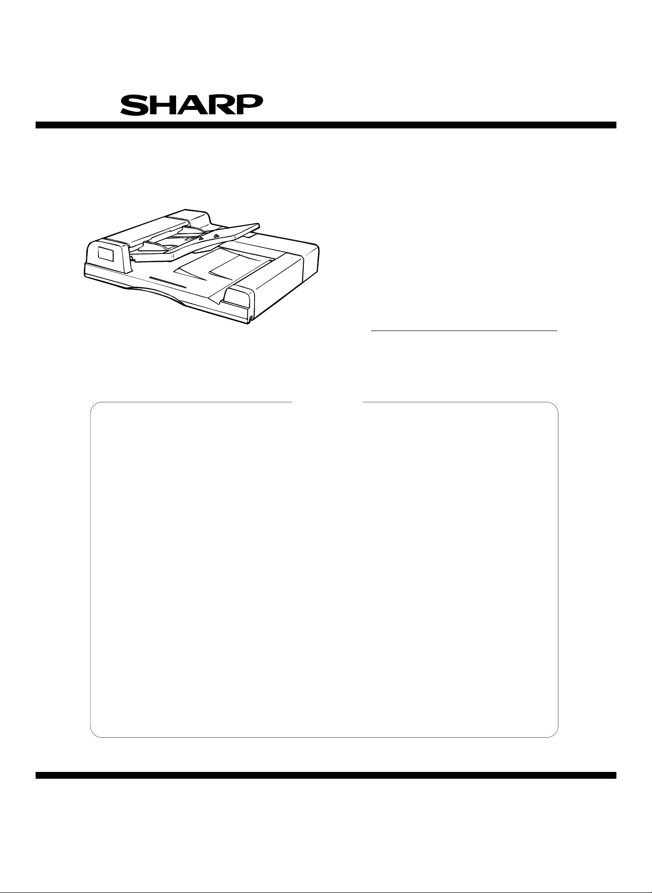
[1] PRODUCT OVERVIEW
The SF-A56/A17 is a reversing automatic document feeder (RADF)/
automatic document feeder (ADF) for the copier SF-2025/2030. The
SF-A56 is capable of automatically copying both sides of document
by inverting the document sheets up-side down, while feeding them.
Even document sheets of different lengths and the same width may
be set in the document tray, an internal sensor in the ADF senses the
document size when the document is fed. The copier automatically
selects the proper copy paper corresponding to the document size
along with the appropriate magnification ratio.
If the appropriate copy paper, respective to the document size and
the magnification ratio, is not available, the copier stops copying and
indicates the required paper size on the display.
[2] SPECIFICATIONS
• Document setting direction: Face-up
• Document setting position: Center alignment
• Document transfer system: Belt drive
• Document feed sequence: Bottom take-up feeding
(Face-up discharge)
• Document size: A3 ∼ A5 (Portrait), 11" × 17" ∼
8-1/2" × 5-1/2"
• Document changing time: 0.68sec or less
(Excluding the first copy)
• Document weight: Thin paper mode; 35 ∼ 50g/m
Standard mode; 51 ∼ 128g/m
• Max. No. of documents to be set:
50 sheets (A4, letter)
35 ∼ 80g/m2 (9 ∼ 21lb), 5mm thick
or less
80 ∼ 128g/m2 (21 ∼ 33lb),
5mm thick or less
• Document stopper: Mechanical stopper
• Dimensions: SF-A56;
592 (W) × 521 (D) × 110 (H)mm
23-5/16" (W) × 20-33/64" (D) ×
4-11/32" (H)
SF-A17;
571 (W) × 521 (D) × 110 (H)mm
22-31/64" (W) × 20-33/64" (D) ×
4-11/32" (H)
• Weight: SF-A56; 11kg (24.3lbs)
SF-A17; 10kg (22.1lbs)
[Features]
• Document detection on tray (Irregular-sized documents are copied
without size recognition.)
• Recognized paper sizes: Japan;
A3, B4, A4, A4R, B5, B5R,
Inch series;
11" × 17", 8-1/2" × 14", 8-1/2" ×
11", 8-1/2" × 11"R, 8-1/2" × 5-1/2"
Non-Japanese A/B series:
A3, B4, A4, A4R, A5
• Mixed document: Possible
• Document inversion: Automatic
[Display]
• Document feed indicator: Lights when documents are set on
feed tray and indicates that RADF is
ready.
2
2
• Remove original indicator: When originals are placed manually,
the LED lights at the same time as
exposure of the last document sheet
is finished. The LED goes out when
the document feed cover is opened.
[3] UNPACKING AND
INSTALLATION
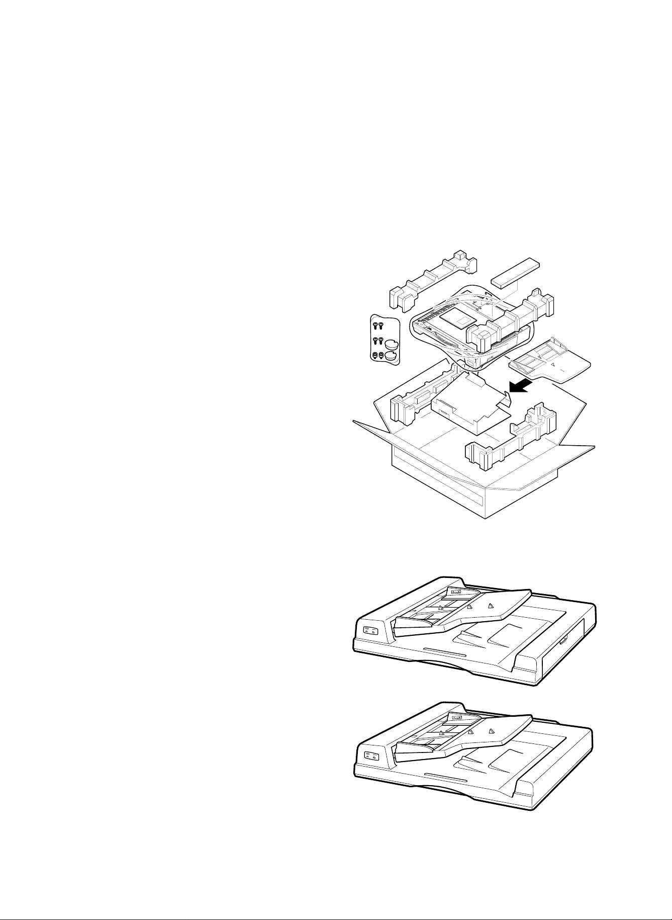
1. UNP ACKING
2. INSTALLATION
SF-A56
SF-A17
– 1 –
Page 3
Included parts
2. Mount the ADF onto the copier.
Remove the two cut-outs from the rear part of the upper cover of the
copier.
Cut-outs
Rear part of
upper cover
ADF tray
ADF mounting screws
(2 pcs.)
Right cover
(1 pc.)
ADF securing screws
(2 pcs.)
Tray securing screws
(2 pcs.)
Left cover
(1 pc.)
Unplug the copier and follow the procedure below.
1. Remove the document cover.
Open the document cover and lift it at a slight backward angle to
remove it.
Insert the left and right covers (included parts) into the holes from
which the document cover has been removed.
Document cover
Right cover
Install the two ADF mounting screws.
ADF mounting screws
Fit the ADF mounting screws into the holes in the hinges of the ADF
and secure the ADF with the two ADF securing screws.
ADF securing screws
Left cover
ADF mounting screw
ADF securing screw
– 2 –
Page 4
3. Adjust the angle of ADF.
Loosen the two securing screws for the angle adjusting panel attached to the hinge angle and then fasten the loosened screws while
raising the angle adjusting panel completely.
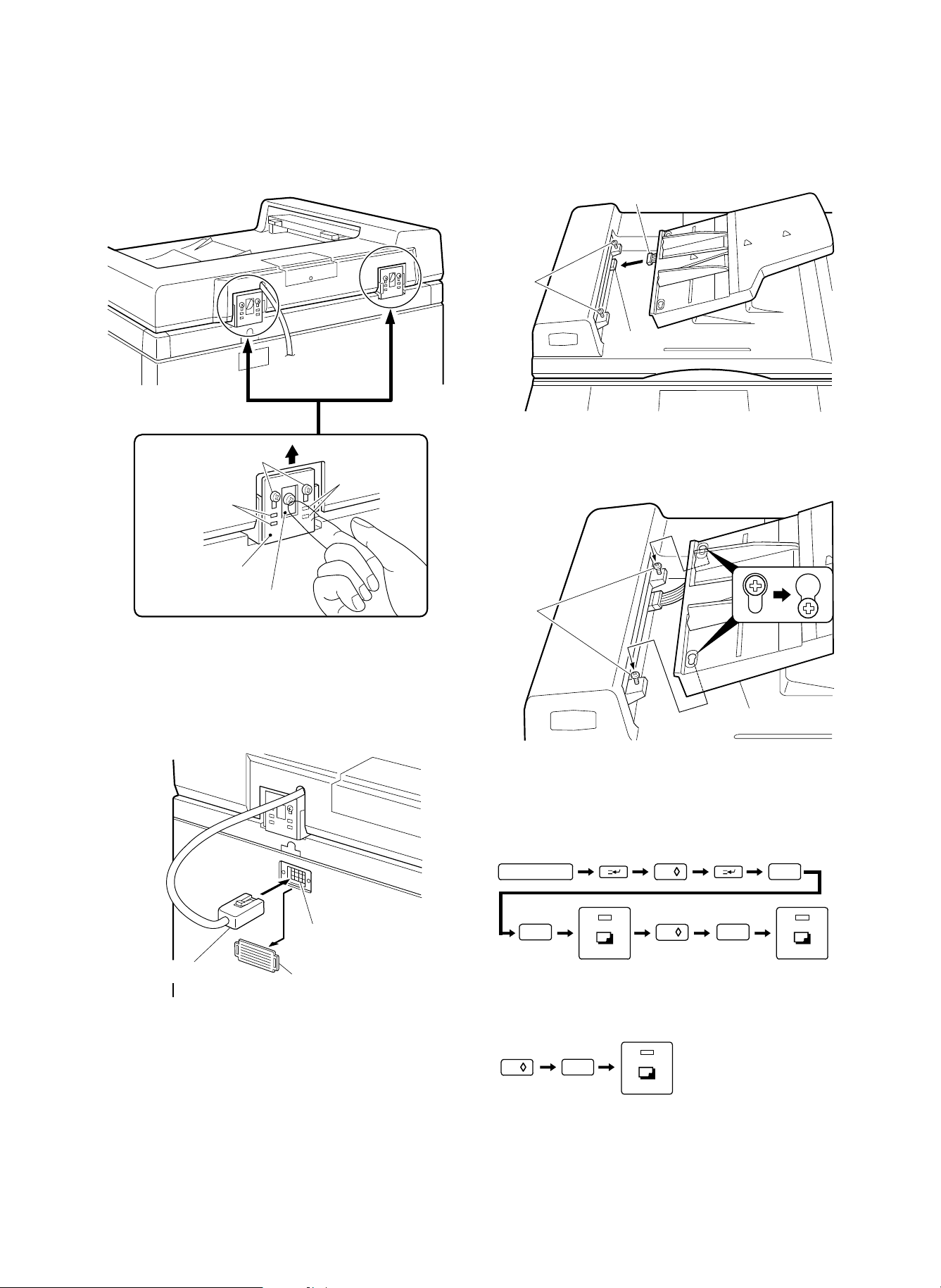
5. Connect the ADF tray connector.
Thread the M4 x 8 tray securing screws (includedparts) partway into
their holes, then connect thetray connector.
Tray connector
Tray
securing
screws
Connector on the ADF
Angle adjusting panel
securing screws
Long hole
Long hole
Hinge
Angle adjusting panel
NOTE:
Be sure to check that the protrusion of the angleadjusting panel
is securely inserted into the long hole of the hinge.
4. Connect the ADF connector.
Remove the connector cover from the copier’s rear cover.
Next, connect the ADF connector to the connector on the copier.
6. Attach the ADF tray.
Loosen the two ADF tray securing screws, install the tray as shown in
the figure, and fasten the tray securing screws.
Tray
securing
screws
Tray
Plug the copier into a grounded outlet and turn the
power switch on. Then, follow the procedure below.
7. Set the mode.
• Operate the copier keys to set the mode.
ADF connector
Connector on the copier
Connector cover
C
5 0
The above key operation will display the currently set mode.
//
//
• When only the SF-A56 is to be set, immediately after the above
key operation, operate the keys as follows:
//
– 3 –
0
1
Page 5
• If the mode is to be set in combination with other options, use the
table shown below to add up the total of the setting values for all
the peripheral devices to be set, and set that total value.
For example, if the SF-A56 and sorter are to be set, the total
setting value is 1 + 10 = 11. Operate the keys as follows:
The leading edge position can be adjusted within a range of 8 mm
(8 steps) on the stopper side and 7 mm (7 steps) on the glass side
in 1 mm increments. Adjustment can be done separately for the
one-sided, two-sided, and thin paper modes.
8
/
0
2
4
3
5
69
00
0/
01 02
03
041
0
0
SF-A17 1 Stand/paper drawer 4 Sorter 10
SF-A56 1 Staple sorter 10
8. Adjust the center of the copy.
Set an original in the ADF tray and make a copy.
When the copy is off center as shown in Fig. 1 or Fig. 2, loosen the
two tray securing screws and adjust the tray by moving it in direction
A orB as shown in the figure.
Mark
Tray securing screw
BA
8
mm
Stopper
6
mm
Glass
View from the operator side
Setup example
(1) If the leading edge of the original was not fed all the way to the
stoppe r, enter value which will mov e the original towa rd the
stopper side.
7, 6, 5, 4...
Original
Stopper
Glass
(2) If the copy image at the leading edge was distorted, enter value
which will move the original toward the glass side.
9, 10, 11...
Original
★ When off center as shown in fig. 1
Move the tray in direction A and secure it with the two mounting
screws. Make a copy to check whether it is centered properly.
Fig. 1
Center of copy paper
Center of original image (first copy)
★ When off center as shown in fig. 2
Move the tray in direction B and secure it with the two mounting
screws. Make a copy to check whether it is centered properly.
Fig. 2
Center of copy paper
Center of original image (first copy)
Stopper
Glass
(3) If the original overrode the stopper, enter value which will move
the original toward the glass side.
9, 10, 11, 12 ...
Original
Stopper
Glass
• After selecting test command 53 , enter a selected set value
between 0 and 15 using the copier keys.
C
0/
0/
(a) One-sided mode
(b) Two-sided mode
(c) One-sided thin paper mode
*For SF-A17, only (a) and (c) are possible.
4
(a)
0
(b)
1
(c)
2
2
9. Adjust the position of the leading edge of originals
• The position of the leading edge of originals fed from the ADF can
be determined using test command 53 .
• Although the leading edge has been factory set to stop at location
(8), it may need to be adjusted depending on the type of originals.
Set to between 0 and 15 as dictated by the copier's performance.
The factory setting is "8".
– 4 –
Page 6
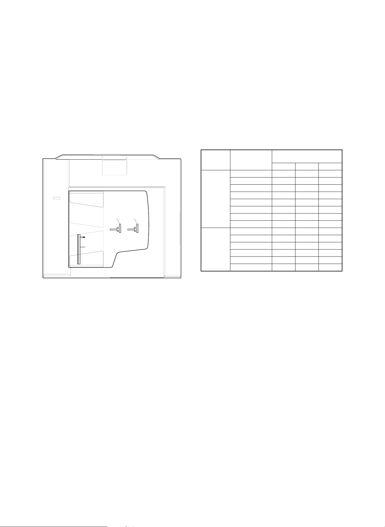
[4] STRUCTURE
A. External fitting
Original guide
Original feed cover
Display lamp
B. Mechanism
Original stopper
Separation
roller
A21 weight plate
Semi-circular roller
Original support
Original transport
cover
Original exit section
cover
Paper exit roller
Flapper
C. PWB distribution
Control PWB
Original reverse
sensor PWB
Original timing
sensor PWB
Separation
roller
Weight plate
Semi-circular roller
Reverse sensor
PWB (SF-A56 only)
LED PWB
Paper feed roller
Paper exit
unit
Resist
roller
Transport belt
drive roller
Paper feed roller
Original transport belt
transport belt
follower roller
SF-A56
Reverse
roller
Resist
roller
Transport belt
Paper exit roller
Original transport belt
Transport belt follower roller
SF-A17
D. Motors, solenoids, and clutches
■ Motors
Code Name Type Functions and operations Contact/output
DFM Paper feed motor DC motor Drives the pickup roller, the separation roller,
DTM Transport motor Stepping motor Drives the transport belt roller.
DRM Reverse motor Stepping motor Drives the reverse roller and the paper exit roller.
DFSOL Paper feed solenoid DC solenoid Presses the paper feed section weight plate onto
DRSOL Reverse solenoid DC solenoid Drives the reverse flapper to select the paper
DTM
and the resist roller.
the original and opens/closes the shutter.
exit path or the reverse feed path.
DRM (SF-A56 only)
When this is ON, the weight
plate and the shutter fall.
When this is ON, the reverse
path is selected.
DFM (SF-A56 only)
DRSOL (SF-A56 only)
DFSOL (SF-A56 only)
– 5 –
Page 7
E. Sensor s, swit ch es, det ect or s
DFMRS
FGOD
DWS
AUOD
DSS
DFD
DLS1
DED
DTD
TGOD (SF-A56 only)
RDD (SF-A56)
DES (SF-A17)
DWVR
Code Name Type Functions and operations Contact/output
DFD Original feed sensor Reflection sensor Turns HIGH when the original lead edge
is fed just in front of the resist roller.
DTD Original timing sensor Reflection sensor Turns HIGH when the original lead edge
is transported from the paper feed section
HIGH when the original is
sensed.
HIGH when the original is
sensed.
to the vicinity of the transport belt.
RDD Reverse sensor Reflection sensor Turns HIGH when the original lead edge
is transported to the reverse/paper exit
HIGH when the original is
sensed.
path.
DED Original end sensor Photo interrupter Final paper detection on the tray LOW when the original is
sensed.
DWVR Original width volume Slide volume Original width detection on the tray
DLS1 Original length sensor 1 Photo interrupter Original length detection on the tray HIGH when the original is
sensed.
DLS2 Original length sensor 2 Photo interrupter Original length detection on the tray (Inch
series only)
HIGH when the original is
sensed.
DSS Original set sensor Photo interrupter Original detection on the tray HIGH when the original is
sensed.
DFMRS Paper feed motor rotation sensor Photo interrupter Paper feed motor rotation detection Pulse output
DWS Original width sensor Photo interrupter Original width detection LOW when the original is
sensed.
AUOD ADF open/close sensor Microswitch ADF unit open/close detection LOW when closed.
FGOD Paper feed guide switch Microswitch Paper feed cover open/close detection LOW when closed.
TGOD Reverse guide switch Microswitch Reverse cover open/close detection LOW when closed.
DES Paper exit sensor Photo interrupter Turns HIGH when the original lead edge
is transported to the paper exit path
HIGH when the original is
sensed.
– 6 –
Page 8
[5] OPERATIONAL DESCRIPTIONS
(MECHANISM SECTION)
A. Operation flowchart
The figures below show the transport path of an original from the
original setting, through paper feed, copying, to paper exit. For details
of operations, refer to the operation process.
Original stopper
Separation
roller
Resist
roller
Separation
roller
Resist
roller
1) SF-A17 ADF mode (single copy mode) copying
Step 01: The transport section is closed. (AUOD OFF)
Step 02: An original is set on the original tray. (DSD
Step 03: Original feed display ON
Step 04: Print SW ON
(Preliminary
paper feed):
Step 05: Paper feed motor (DFM) forward rotation
Step 06: Transport motor (DTM) forward rotation
A21 weight plate
Semi-circular roller
Transport belt
drive roller
Paper feed roller
Weight plate
Semi-circular roller
Transport belt
Paper exit roller
START
↓
↓
↓
↓
↓
↓
↓
Paper exit roller
Flapper
Original transport belt
transport belt
SF-A56
Original transport belt
SF-A17
output HIGH)
For the first original, dummy paper exit is
performed.
(Paper feed roller, semi-circular roller
rotation)
Since the stopper is up, paper feed is not
performed.
(Transport belt, paper exit roller rotation)
* A: If there have been some originals on
the tray, they are discharged.
follower roller
Paper feed roller
Transport belt follower roller
Reverse
roller
Paper exit
unit
↓
Step 07: Paper feed motor (DFM) OFF
↓
Step 08: Paper feed solenoid (DFSOL) ON
↓
Step 09: Paper feed motor (DFM) forward rotation
↓
* A Step 10: The paper exit sensor (DES) senses the lead
↓
* A Step 11: Transport motor (DTM) rpm down
↓
Step 12: The original feed sensor (DFD) senses the
↓
Step 13: The original is stopped by the resist roller and
↓
Step 14: Paper feed motor (DFM) reverse rotation
↓
Step 15: The original width sensor (DWS) senses the
↓
Step 16: The original timing sensor (DTD) senses the
↓
Step 17: Paper feed motor (DFM) OFF
↓
* A Step 18: Paper exit sensor (DES) senses the paper
↓
* A Step 19: Original discharge
↓
Step 20: Transport motor (DTM) OFF
↓
(Paper feed)
↓
Step 21: Transport motor (DTM) forward rotation
↓
Step 22: Paper feed motor (DFM) reverse rotation
↓
Step 23: Original width sensor (DWS) output HIGH
↓
Step 24: Original timing sensor (DTD) senses the
(The weight plate and the stopper move down
to press the original onto the semi-circular
roller.)
The original feed is started.
edge of the discharged original.
(DES output HIGH)
lead edge of the original. (DFD output HIGH)
the paper feed motor (DFM) is turned OFF.
(Resist roller rotation)
The original lead edge is taken up by the
resist roller.
original width. (Output LOW)
original lead edge. (DTD output HIGH)
(The original is stopped with its lead edge
taken up by the resist roller.)
exit rear edge. (DES output LOW)
(The transport belt and the paper exit roller
are stopped.)
(The transport belt and the paper exit roller
rotate.)
(Resist roller rotation)
The original is sent to the transport section.
original rear edge. (DFD output LOW)
– 7 –
Page 9

↓
Step 25: Paper feed motor (DFM) OFF
↓
Step 26: Transport motor (DTM) OFF
↓
* B Step 27: Paper feed solenoid (DFSOL) OFF
↓
Step 28: Copier mirror base scanning is started.
↓
* E
DSS
↓
(Preliminary
paper feed)
↓
Step 29: Paper feed motor (DFM) forward rotation
↓
Step 30: The original feed sensor (DFD) senses the
↓
Step 31: The original is stopped by the resist roller.
↓
Step 32: Paper feed motor (DFM) reverse rotation
↓
Step 33: The original width sensor (DWS) senses the
↓
Step 34: The original timing sensor (DTD) senses the
↓
Step 35: Paper feed motor (DFM) OFF
↓
Step 36: Copier mirror base scanning is stopped.
↓
(Paper exit)
↓
Step 37: Transport motor (DTM) forward rotation
↓
* D Step 38: The previous original discharge
↓
Step 39: Paper feed motor (DFM) reverse rotation
(Resist roller stops.)
(Transport belt, paper exit roller stop)
Original stop
(The weight plate and the stopper move up.)
* B: If there is no original on the tray, move
up the stopper and the weight plate.
LOW (No original on the tray) → After
completion of mirror base scanning, go to
step 48.
HIGH (There are some originals on the tray.)
↓
(Paper feed roller, semi-circular roller rotation)
The original feed is started.
original lead edge. (DFD output HIGH)
Paper feed motor (DFD) OFF
(Resist roller rotation)
The original lead edge is taken up by the
resist roller.
original.
(Output HIGH)
original lead edge. (DTD output HIGH)
(The original is stopped with its lead edge
taken up by the resist roller.)
(Transport belt, paper exit roller rotation)
The original discharge is started.
(Resist roller rotation)
The original is sent to the transport section.
↓
Step 40: Paper exit sensor (DES) senses the original
↓
Step 41: Original width sensor (DWS) output HIGH
↓
Step 42: Original timing sensor (DTD) senses the
↓
Step 43: Paper feed motor (DFM) OFF
↓
Step 44: Paper exit sensor (DES) senses the
↓
* D Step 45: Transport motor (DTM) OFF
↓
Step 46: Paper feed solenoid (DFSOL) OFF
↓
Step 47: Copier mirror base scanning is started.
* E ↓
DSS
↓
Step 48: Transport motor (DTM) forward rotation
↓
* D Step 49: Previous original discharge
↓
Step 50: Paper exit sensor (DES) senses the
↓
Step 51: Transport motor (DTM) rpm down
↓
Step 52: Paper exit sensor (DES) senses the
↓
Step 53: Original discharge
↓
Step 54: Transport motor (DTM) OFF
↓
END
Note: * A: This operation is performed when there is an original on
the original table in advance. If there is no original on
the original table, this operation is not performed.
* B: This operation is performed when there is no original on
the original table.
* C: When the is an original on the original tray, the original
set sensor (DSD) output becomes LOW.
* D: When the previous original remains in the paper exit
section, it is discharged.
rear edge. (DES output HIGH)
original rear edge. (DTD output LOW)
(Resist roller stop)
discharged original rear edge. (DES output
LOW)
(Transport belt, paper exit roller stop)
Original stop
(The weight plate and the stopper move up.)
* B: When there is no original on the tray,
move up the stopper and the weight
plate.)
HIGH (There are some originals on the tray.)
→ Go to step 29 (Preliminary paper feed).
LOW (No original on the tray)
(Transport belt, paper exit roller rotation)
discharged original lead edge. (DES output
HIGH)
discharged original rear edge. (DES output
LOW)
(Transport belt, paper exit roller stop)
– 8 –
Page 10

2) SF-A56 RAD mode (duplex copy mode) copying
START
↓
Step 01: The transport section is closed. (AUOD ON)
↓
Step 02: An original is set on the original tray. (DSS
↓
Step 03: Original feed display ON
↓
Step 04: Print SW ON
↓
(Preliminary
paper feed):
↓
* A Step 05: Paper feed motor (DFM) forward rotation
↓
Step 06: Reverse motor (DRM) forward rotation
↓
Step 07: Transport motor (DTM) rotation
↓
* A Step 08: Paper feed motor (DFM) OFF
↓
Step 09: Paper feed motor (DFM) forward rotation
↓
* B Step 10: Reverse sensor (RDD) senses the lead edge
↓
Step 11: Original feed sensor (DFD) senses the lead
↓
Step 12: Paper feed motor (DFM) OFF
↓
Step 13: Paper feed motor (DFM) reverse rotation
↓
Step 14: Original width sensor (DWS) senses the
↓
Step 15: Original timing sensor (DTD) senses the lead
output HIGH)
* A: For the first original, dummy paper exit
is performed.
(Paper feed roller, semi-circular roller
rotation)
Since the stopper is up, paper feed is not
performed.
(Reverse roller, paper exit roller rotation)
(Transport belt rotation)
* B: If there has been an original on the
tray, is discharged.
Paper feed solenoid (DFSOL) ON
(The weight plate and the stopper move down
to press the original onto the semi-circular
roller.)
(Paper feed roller, semi-circular roller
rotation)
The original feed is started.
of the discharged original.
(RDD output HIGH)
edge of the discharged original. (DFD output
HIGH)
The original is stopped by the resist roller.
(Resist roller rotation)
The lead edge of the original is taken up by
the resist roller.)
original width. (Output LOW)
edge of the original. (DTD output HIGH)
↓
Step 16: Paper feed motor (DFM) OFF
↓
* B Step 17: Reverse sensor (RDD) senses the rear edge
↓
Step 18: Transport motor (DTM) OFF
↓
* B Step 19: Original discharge
↓
Step 20: Reverse motor (DRM) OFF
↓
(Preliminary
paper feed):
↓
Step 21: Transport motor (DTM) forward rotation
↓
Step 22: Paper feed motor (DFM) reverse rotation
↓
Step 23: Original feed sensor (DFD)
↓
* C Step 24: Paper feed solenoid (DFSOL) OFF
↓
Step 25: Original width sensor (DWS) output HIGH
↓
Step 26: Original timing sensor (DTD) senses the rear
↓
Step 27: Reverse sensor (RDD) senses the lead edge
↓
Step 28: The lead edge of the original is moved
↓
Step 29: Transport motor (DTM) OFF
↓
Step 30: Reverse motor (RDM) OFF
(The original is stopped with its lead edge
taken up by the resist roller.)
of the discharged original. (RDD output LOW)
Reverse motor (DRM) rpm down
(Transport stop)
(Reverse roller, paper exit roller stop)
(Paper feed reverse)
Transport motor, reverse motor (DRM)
forward rotation (Reverse roller, paper exit
roller rotation)
(Resist roller rotation)
The original is sent to the transport section.
Senses the rear edge of the discharged
original. (DFD output LOW)
(The weight plate and the stopper move up.)
* C: If there is no original on the original
tray, move up the stopper and the
weight plate.
edge of the original.
(DTD output LOW)
Paper feed motor (DFM) OFF (Resist roller
stop)
Reverse solenoid (DRSOL) ON (The flapper
move up.)
of the original. (RDD output HIGH)
counterclockwise by the flapper.
(Transport belt stop)
(Reverse roller, paper exit roller stop)
– 9 –
Page 11

↓
Step 31: Transport motor (DTM) OFF
↓
Step 32: Reverse motor (DRM) forward rotation
↓
Step 33: Paper exit sensor (RDD) senses the rear
↓
Step 34: Reverse motor (DRM) OFF
↓
Step 35: Transport motor (DTM) OFF
↓
Step 36: Reverse solenoid (DRSOL) OFF
↓
Step 37: Copier mirror base scanning is started.
* D ↓
DSS output
↓
(Preliminary
paper feed)
↓
Step 38: Paper feed motor (DFM) forward rotation
↓
Step 39: Original feed sensor (DFD) senses the lead
↓
Step 40: Paper feed motor (DFM) OFF
↓
Step 41: Paper feed motor (DFM) forward rotation
↓
Step 42: Original width sensor (DWS) senses the
↓
Step 43: Original timing sensor (DTD) senses the lead
↓
Step 44: Paper feed motor (DFM) OFF
↓
Step 45: Copier mirror base scanning stop
↓
(Transport belt rotation)
(Reverse roller, paper exit roller rotation)
The original is transported to the paper feed
section.
edge of the reverse original.
(RDD output LOW)
(Reverse roller, paper exit roller stop)
(Transport belt stop)
Original stop
(The flapper moves down.)
LOW (There is no original on the tray.) →
After completion of mirror base scanning, go
to step 64. (Reverse rotation)
HIGH (There is an original on the tray)
↓
(Paper feed roller, semi-circular roller
rotation)
The original feed is started.
edge of the original.
(DFD output HIGH)
The original is stopped by the resist roller.
(Resist roller rotation)
The lead edge of the original is taken up by
the resist roller.
original width. (Output LOW)
edge of the original. (DTD output HIGH)
(The original is stopped with its lead edge
taken up by the resist roller.)
↓
(Reverse
rotation)
↓
Step 46: Reverse solenoid (DRSOL) ON
↓
Step 47: Transport motor (DTM) forward rotation
↓
Step 48: Reverse sensor (RDD) senses the lead edge
↓
Step 49: The lead edge of the original is moved
↓
Step 50: Transport motor (DTM) OFF
↓
Step 51: Reverse motor (DRM) OFF
↓
Step 52: Transport motor (DRM) reverse rotation
↓
Step 53: Reverse motor (DRM) reverse rotation
↓
Step 54: Reverse sensor (RDD) senses the rear edge
↓
Step 55: Reverse motor (DRM) OFF
↓
Step 56: Transport motor (DTM) OFF
↓
Step 57: Reverse solenoid (DRSOL) OFF
↓
Step 58: Copier mirror base scanning start
↓
Step 59: Copier mirror base scanning stop
* E ↓
First-out
original
↓
(Paper exit
paper feed
reverse)
(The flapper moves up.)
(Transport motor rotation)
Reverse motor (DRM) forward rotation
(Rreverse roller, paper exit roller rotation)
of the original.
(RDD output HIGH)
counterclockwise by the flapper.
(Transport belt stop)
(Reverse roller, paper exit roller stop)
(Transport belt rotation)
(Reverse roller, paper exit roller rotation)
The original is transported to the paper feed
section.
of the reversed original.
(RDD output LOW)
(Reverse roller, paper exit roller stop)
(Transport belt stop)
Original stop
(The flapper moves down)
NONE → After completion of mirror base
scanning, go to step 82.
YES
↓
– 10 –
Page 12

↓
Step 60: Transport motor (DTM) forward rotation
↓
Step 61: Paper feed motor (DFM) reverse rotation
↓
Step 62: Original feed sensor (DFD) senses the rear
↓
* C Step 63: Paper feed solenoid (DFSOL) OFF
↓
Step 64: Original width sensor (DWS) output LOW
↓
Step 65: Original timing sensor (DTD) senses the rear
↓
Step 66: Reverse sensor (RDD) senses the lead edge
↓
Step 67: Transport motor (DTM) rpm down
↓
Step 68: Original discharge
↓
Step 69: Reverse solenoid (DRSOL) ON
↓
Step 70: Transport motor (DTM) forward rotation
↓
Step 71: Reverse sensor (RDD) senses the lead edge
↓
Step 72: The lead edge of the original is moved
↓
Step 73: Transport motor (DTM) OFF
↓
Step 74: Reverse motor (DRM) OFF
↓
Step 75: Transport motor (DTM) reverse rotation
↓
Step 76: Reverse motor (DRM) forward rotation
(Transport belt rotation)
Reverse motor (DRM) forward rotation
Reverse roller, paper exit roller rotation)
The original is discharged.
(Resist roller rotation)
The original is sent to the transport section.
edge of the original.
(DFD output LOW)
(The weight plate and the stopper moves up.)
* C: When there is no original on the tray,
move up the stopper and the weight
plate.
edge of the original. (DTD output LOW)
of the discharged original.
(RDD output HIGH)
(The flapper moves up.)
(Transport belt rotation)
Reverse motor (DRM) forward rotation
(Reverse roller, paper exit roller rotation)
of the original.
(RDD) output HIGH)
counterclockwise by the flapper.
(Transport belt stop)
(Reverse roller, paper exit roller stop)
(Transport belt rotation)
(Reverse roller, paper exit roller stop)
The original is sent to the paper feed section.
↓
Step 77: Reverse sensor (RDD) senses the rear edge
↓
Step 78: Reverse motor (RDD) senses the rear edge
↓
Step 79: Transport motor (DTM) off
↓
Step 80: Reverse solenoid (DRSOL) OFF
↓
Step 81: Copier mirror base scanning start
* D
Note: * A: For the first original, the preliminary paper feed opera-
↓
DSS output
↓
(Paper exit)
↓
Step 82: Transport motor (DTM) forward rotation
↓
Step 83: Reverse sensor (RDD) senses the lead edge
↓
Step 84: Reverse sensor (RDD) senses the rear edge
↓
Step 85: Original discharge
↓
Step 86: Reverse motor (DRM) OFF
↓
END
tion is performed.
* B: When there is an original on the original tray in ad-
vance, it is discharged.
* C: When there is no original on the original tray, move up
the weight plate and the stopper.
* D: When there is no original on the original tray, the origi-
nal set sensor (DSS) output becomes LOW.
* E: It depends on whether there is any preliminary fed origi-
nal in step 38 ∼ step 44.
of the reverse original. (RDD output LOW)
of the reversed original. (RDD output LOW)
(Transport belt stop)
Original stop
(The flapper moves down.)
LOW (No original on the tray) → After
completion of mirror base scanning, go to
step 46 (reverse).
HIGH (There is an original on the tray.) → Go to
step 38 (Preliminary paper feed).
↓
(Transport belt rotation)
Reverse motor (DRM) forward rotation
(Reverse roller, paper exit roller rotation)
The original is discharged.
of the discharged original.
(RDD output HIGH)
of the discharged original.
(RDD output LOW)
Transport motor (DTM) OFF
(Transport belt stop)
Reverse motor (DRM) rpm down
(Reverse roller, paper exit roller stop)
– 11 –
Page 13
B. Original size detection
The original size is detected in three ways of different purposes.
1) Original size detection by the original set tray
The original size detection by the original set tray is used in automatic
paper size and automatic magnification selection mode, in order to
recognize the original size when the original is set on the original tray,
allowing the automatic selection of paper size and magnification ratio
of copy.
When originals composed of sheets of different sizes are set, this
detection method recognizes the largest sheet as the original size,
which is determined by the width measured by the original width
volume (DWVR) and the length measured by the original length sensors (DLS1, DLS2).
The original size is determined in the timing of original sensing by the
original set sensor (DSS).
DLS1 DLS2
DWVR
AB series
Inch series
Document size,
setting orientation
A4 3 ● —
B5 4 ● —
A5 5 ● —
A5R 7 ● —
B5R 6 | —
A4R 5 | —
B4 4 | —
A3 3 | —
11" × 8.5" 0 ●●
8.5" × 5.5" 1 ●●
8.5" × 5.5"R 2 ●●
11" × 8.5R" 1 | ●
14" × 8.5" 1 ||
11" × 17" 0 ||
F: ON or L output (sensed)
●: OFF or H output
DWVR DLS1 DLS2
– 12 –
Page 14

2) Original size detection by the original width sensor
(DWS) in the paper feed section
The original size detection by the original width sensor (DWS) in the
paper feed section is used in automatic paper size and automatic
magnification ration selection mode to determine whether the original
is A4 or A5 (11" x 8.5" or 8.5" x 5.5").
When originals composed of stacked sheets of different sizes are set
in the original tray, the original size cannot be detected by the sensors in the original tray. Therefore, this function is provided to sense
the original size behind the resist roller after the paper feed section
has fed the original, as far as originals of A4 or A5 size (11" x 8.5" or
8.5" x 5.5") (portrait) is concerned. Consequently, if A4- and A5-size
(11" x 8.5" or 8.5" x 5.5") originals (portrait) are stacked and set in the
original tray, the original size detection by the paper feed section
original width sensor (DWS) has the priority over the original size
detection by the original set tray.
When A4- and A5-size (11" x 8.5" and 8.5" x 5.5") originals (portrait)
are stacked and set in the original tray, the original length sensors
(DSL1, DSL2) are not actuated. Therefore, the original width is
sensed by the paper feed section original width sensor (DWS) to
judge A4 or A5 (11" x 8.5" or 8.5" x 5.5").
Paper feed section original width sensor (DWS)
A4
B5
Paper feed section original width sensor (DWS)
11"x8.5"
8.5"x5.5"
Paper feed section original width sensor (DWS)
Paper feed section original width sensor (DWS) status
Original size
A4 |
B5 ●
F: Output LOW (Detection)
●: Output HIGH
Paper feed section original width sensor (DWS)
Paper feed section original width sensor (DWS) status
Original size
11" × 8.5" |
8.5" × 5.5" ●
– 13 –
F: Output LOW (Detection)
●: Output HIGH
Page 15

3) Original size detection by the paper feed motor
rotation sensor (DFMRS)
This function compensates for the inaccuracy of the original size
recognition in the original tray when originals of different sizes are
stacked in the original tray. That is, results of this function has priority
over the original size detection in the original tray. The pulses of the
slit disc rotation of the feed motor (DFM) are counted in the period
before the rear edge of original is sensed (DFD output LOW) by the
original feed sensor after the feed motor (DFM) has started reverse
rotation, that is, after the resist roller has started rotating and feeding
of original from the fed section to the transport section has been
started, to determine the original length.
To improve detection accuracy, the original width is sensed also by
the paper feed section original width sensor (DWS).
Resist roller rotation start (The original is fed from the paper feed
section.)
Original feed sensor (DFS)
A
[6] DISASSEMBLY, ASSEMBLY AND
ADJUSTMENT
* Descriptions in this chapter excludes simple disassembly and as-
sembly operations. Refer to the parts guide for the disassembly ad
assembly of parts which are not explained here.
* Refer to the description in [7] ACTUAL WIRING DIAGRAM for the
processing of the wiring during assembly.
1. Transport section opening
1 Loosen two screws which are fixing the hinge stopper to allow the
hinge stopper to move.
2 Slide the hinge stopper downward by using the step screw, fit the
dove with the hole and tighten the two fixing screws which were
loosen before.
3 Open the transport section.
Resist roller
Original feed sensor (DFD)
B
Resist roller
The paper feed motor rotation sensor (DFMRS) counts the number of
rotations of the paper feed motor (DFM) between A and B to judge
the original length.
Original feed sensor (DFS)
detects the original rear edge.
Screw (Loosen.)
Hinge stopper (Move down.)
– 14 –
Page 16

2. Belt unit dis asse mb ly
3. Paper feed unit disassembly
1 Open the transport section.
2 Remove two screws as shown in the figure below, and remove the
belt unit as shown with arrow A and arrow B in this sequence.
A
Screw
(Loosen.)
Belt unit
1 Open the transport section.
2 Remove the tray. (Refer to the installing procedure.)
3 Remove four screw which are fixing the lower cover, and remove
the blower cover.
4 Remove the five fixing screws of the paper feed unit, open the
paper feed cover, and remove the fixing screw.
Paper feed
cover
Paper feed unit
fixing screw
(Loosen.)
Paper feed unit
fixing screws
Paper feed unit
Lower cover
5 Remove the paper feed motor drive belt, and remove the four
harness connectors. Then remove the paper feed unit.
B
Harness
connector
(Remove.)
Paper feed
unit
Paper feed motor
drive belt (Remove.)
Paper feed
motor
– 15 –
Page 17

4. Paper exit un it dis asse mb ly
1 Open the transport section and remove the lower cover.
2 Remove the five fixing screw of the paper exit unit.
3 Remove the paper exit unit harness connector from the control
PWB, and pull out the harness from the edge saddle shown in the
figure below. Then remove the paper exit unit.
3 Remove two screws from the separation unit, and remove the
separation roller holder unit.
Screw
(Remove.)
Edge saddle
Screw
SF-A56 SF-A17
Screw
Separation roller
holder unit
Reverse
unit
4 Remove two springs from the separation roller holder, and remove
the bearing and the slide bearing. Remove the separation roller
and the spring clutch.
Spring
(Remove.)
5. Separation roller disassembly
1 Open the paper feed cover.
2 Remove two fixing screws of the separation unit, and remove the
separation unit.
Screw (Remove.)
Separation unit
Slide shaft
bearing
Separation roller
Spring clutch
Shaft bearing
– 16 –
Page 18

6. Semi-circular roller, paper feed roller
disassembly
1 Open the paper feed cover.
2 Loosen two fixing screws of the tray guide top, and remove two
fixing screws of the side.
3 Remove the harness from the tray guide upper, and remove the
tray guide.
(Be careful not to scratch the harness.)
7. Open/close switch attachment
When closing the transport section from the open state, adjust the
DF open SW plate so that the clearance between the glass surface
and the DF spacers L and R (front side) is 10 ∼ 40mm. Then tighten
the fixing screw.
Side fixing screw
(Remove.)
Tray guide
Side fixing
screw
(Remove.)
Harness
(Remove.)
Top fixing screw
(Remove.)
4 Remove the snaps from the both ends of the pickup shaft and the
separation shaft. (2 kinds of snaps)
5 Remove the pickup shaft bearing and the separation shaft bearing
on the front frame side.
6 Slide the pickup shaft toward the rear frame, and pull out the front
frame side from the chassis.
7 Remove the shaft stopper and the parallel pin from the pickup
shaft and remove the semi-circular shaft.
8 Slide the separation shaft toward the rear frame, and pull out the
front frame side from the chassis.
9 Remove the shaft stopper from the separation shaft, and remove
the paper feed roller.
10~40mm
Microswitch
Fixing
screw
DF open SW plate
8. Original transport belt replacement
1 Remove the belt unit.
2 Remove the two screws shown in the figure below to allow the
belt tension plate to be moved. Remove the transport belt with the
left and the right in parallel.
Original
transport
belt
Shaft stop
Pickup shaft
Snap
Rear frame
side
Semi-circular roller
Parallel pin
Separation shaft
Snap
Bearing
Paper feed
roller
Front frame
side
Shaft stop
Screw
(Remove.)
Belt tension plate
– 17 –
Page 19

[Note for assembly]
1 When installing the original transport belt, put the right and left in
parallel, and allow the same clearance between the spacer and
the belt in the front side and in the rear side.
Spacer
Belt unit
Spacer
Spacer
Spacer
[7] CONNECTOR LAYOUT
1. Control PWB peripheral
IF harness
Control PWB
RU harness
2 Check that the original transport belt is not on the belt guide.
Belt guide
Transport belt
Transport belt
Belt guide
Drive R harness
Drive I/F harness
Control PWB
Control PWB
TR1 harness
SNR harness
SENSOR I/F
harness
Transport motor (DTM)
LED harness
SENSOR I/F
harness
Drive I/F harness
– 18 –
Page 20

2. Paper feed motor peripheral
4. Reverse un it sect io n (Fro nt side)
Paper feed motor (DFM)
Paper feed motor
rotation sensor
Original set
sensor (DSS)
TR2 harness
Drive F harness
SENSOR 2 harness
SENSOR harness
Paper feed
guide switch
(FGOD)
RU harness
Reverse solenoid (DRSOL)
5. Reverse un it sect io n (Rear side )
Reverse guide switch
(TGD)
Reverse motor (DRM)
Paper feed motor
(DFM)
Paper feed motor rotation
sensor (DRMRS)
3. Paper feed section (Front side)
Control PWB
RU harness
SENSOR 2
harness
Drive R harness
6. Tray inside
Original length sensor 2 (DLS2)
Inch series
Original length sensor 1 (DLS1)
Tray harness
Original end
sensor (DED)
Paper feed solenoid (DFSOL)
SOL harness
Original width volume
sensor (DWVR)
– 19 –
Page 21

[8] REPLACEMENT PARTS AND
MAINTENANCE
1. Replacement parts
2. Mode setting in the test mode when supplying the power
Switch ON OFF
Push switch RADF individual unit
operation test mode
DIP switch 1 For AB series For inch series
DIP switch 2 Thin paper mode Normal paper mode
PPC main body
connection mode
Part name Replacement timing
Separation roller 100K copies
Transport belt 100K copies
2. Maintenance parts (Cleaning at every
10K copies)
Clean the parts shown in the table below at maintenance as specified
in the table.
Part name Cleaning method
Original set sensor (DSS) Air blow
Original feed sensor (DFD) Air blow
Original timing sensor (DTD) Air blow
Original width sensor (DWS) Air blow
Paper exit sensor (DES) Air blow
Reverse sensor (RDD) Air blow
Paper feed roller Wipe with alcohol.
Semi-circular roller Wipe with alcohol.
Resist roller Wipe with alcohol.
Paper exit roller Wipe with alcohol.
Reverse roller Wipe with alcohol.
3. Kinds of test modes and DIP switch setting
No. Test mode DIP switch
1 Single paper pass mode All OFF
2 Duplex paper pass mode 1 is ON, all the others
OFF
3 Single aging mode 1 and 3 ON; 2, 4, and 5
4 Duplex aging mode 4 ON, all the others OFF
5 Single paper pass mode
(Thin paper mode)
6 Duplex paper pass mode
(Thin paper mode)
7 Load check mode 1, 5 ON; 2, 3, 4 OFF
8 EEPROM initializing mode
+ all sensors adjustment
mode
10 Resist sensor adjustment
mode
11 Timing sensor adjustment
mode
12 Paper reverse sensor
adjustment mode
* "5" and "6" are for thin paper mode (only in Japan).
OFF
3, 4 ON; 2, 5 OFF
1, 3, 4 ON; 2, 5 OFF
3, 5 ON; 1, 2, 4 OFF
4, 5 ON; 1, 2, 3 OFF
1, 4, 5 ON; 2, 3 OFF
3, 4, 5 ON; 1, 2 OFF
3. DIP switch
The DIP switch on the control PWB shown below allows the individual
operation check of the RADF (ADF).
(1) Control PWB outline
DRIVER FOR MOTOR
DIP SW
CPU
(2) DIP switch outline
OFF
ON
SW No.1 2 3 4 5
1. Entering the test mode:
While pressing the push switch on the control PWB, supply the
power, and the machine will enter the test mode.
DRIVER FOR MOTOR
Push SW
EEPROM
G/A
4. Detail s of the test modes
Set the DIP switch on the control PWB, and open/close the DF to set
the test mode.
Setting of the original size series (AB/Inch) and of normal/thin paper
mode should be performed only when supplying the power.
(1) Single paper pass mode (paper present)
When originals are set on the paper feed tray, the original feed LED
lights up. When the push switch is pressed, all the originals on the
tray are fed.
(2) Duplex paper pass mode (paper present)
When originals are set on the paper feed tray, the original feed LED
lights up. When the push switch is pressed, all the originals on the
tray are fed.
(3) Single aging mode (without paper)
When the push switch is pressed, aging is started. The operation
timing is determined by size detection of each original size.
(4) Duplex aging mode (without paper)
When the push switch is pressed, aging is started. The operation
timing is determined by size detection of each original size.
(5) Thin paper single paper pass mode
When originals are set on the paper feed tray, the original feed LED
lights up. When the push switch is pressed, all the originals on the
tray are fed.
– 20 –
Page 22

(6) Thin paper duplex paper pass mode
When originals are set on the paper feed tray, the original feed LED
lights up. When the push switch is pressed, all the originals on the
tray are fed.
(7) Load check mode
Every time when the push switch pressed, the following operation is
performed in sequence repeatedly.
1. Read LED/Original remain LED ON, paper feed motor reverse
rotation (500mm/sec)
2. Operation stop
3. Ready LED/Original remain LED ON, paper feed motor forward
rotation (250mm/sec)
4. Operation stop
5. Ready LED/Original remain LED ON, electromagnetic clutch
ON, transport motor forward rotation (800mm/sec)
6. Operation stop
7. Ready LED/Original remain LED ON, electromagnetic clutch
ON, transport motor forward rotation (250mm/sec)
8. Operation stop
9. Ready LED/Original remain LED ON, electromagnetic clutch
ON, transport motor forward rotation (800mm/sec)
10. Operation stop
11. Ready LED/Original remain LED ON, electromagnetic clutch
ON, transport motor forward rotation (250mm/sec)
12. Operation stop
13. Ready LED/Original remain LED ON, electromagnetic clutch
ON, paper feed motor synchronization forward rotation
(800mm/sec)
14. Operation stop
15. Ready LED/Original remain LED ON, shutter solenoid ON
16. Operation stop
17. Ready LED/Original remain LED ON, weight solenoid ON
18. Operation stop
19. Ready LED/Original remain LED ON, electromagnetic clutch ON
20. Operation stop
21. Ready LED/Original remain LED ON, electromagnetic brake ON
22. Operation stop
23. Ready LED/Original remain LED ON, flapper solenoid ON
24. Operation stop
25. Ready LED/Original remain LED ON, shutter solenoid ON,
weight solenoid ON, paper feed motor reverse rotation
(500mm/sec)
26. Operation stop
Return to 1.
(9) Resist sensor adjustment mode
(10) Timing sensor adjustment mode
(11) Paper reversing sensor adjustment mode
When the push switch pressed, the adjustment of each sensor is
started. At that time, the LED blinks in the cycle of 100msec. After
completion of the adjustment, the LED turns ON. If there is an error in
the adjustment, the LED blinks in the cycle of 100msec.
JAM, error kinds LED display
Sensor adjustment
upper limit error
Sensor adjustment
lower limit error
Original remain LED blinks in the cycle
of 100msec. Ready LED goes off.
Original remain LED goes off. Ready
LED blinks in the cycle of 100msec.
5. Kinds of errors (RADF single mode
only)
The table below lists the kinds of JAM errors and LED display examples.
To cancel the JAM/motor lock errors, cancel the JAM and open/close
the ADF, or supply the power again.
JAM error kinds LED display
Not reached/remaining JAM in the
paper feed section
Not reached/remaining JAM in the
paper feed section
Paper feed motor lock error Original remain LED blinks
Paper exit motor lock error Ready LED blinks in the
Resist/timing sensor adjustment
error (when supplying the power)
Paper reversing sensor adjustment
error (when supplying the power)
Original remain LED blinks
in the cycle of 100msec.
Ready LED blinks in the
cycle of 100msec.
in the cycle of 200msec.
cycle of 200msec.
Original remain LED blinks
in the cycle of 100msec.
Ready LED blinks in the
cycle of 100msec.
(8) EEPROM initializing + all sensors adjustment
mode
When the push switch is pressed, the EEPROM is initialized. At that
time, the LED blinks in the cycle of 100msec. After completion of
initializing of the EEPROM, the LED turns ON. If there is an error in
initializing of the EEPROM, the LED goes off. After initializing the
EEPROM, adjust the resist sensor, the timing sensor, and the paper
reversing sensor.
JAM, error kinds LED display
EEPROM initializing error Ready LED/Original remain
LED OFF
– 21 –
Page 23

[9] ELECTRICAL SECTION
1. Genera l
This circuit controls feeding, stopping, and reversing of the original. It is composed of sensors, switches, the circuit which processes signals from the
copier PPC, the circuit which drives motors, solenoids, and clutches, the CPU, the G/A and its peripheral circuits.
2. Block diagram
DFD
DTD
DFMRS
DWVR
DWS
DLS1
DLS2
DED
TXD
RXD
DTR
DSR
RES
SGND
Communication
I/O circuit
Original feed
sensor input
circuit
Timing sensor
input circuit
DIP switch
push switch
Paper feed motor
rotation sensor
input circuit
Original width
volume input
circuit
Original width
sensor input
circuit
Original length
sensor input
circuit
Original end
sensor input
circuit
CPU
(IC11)
Display LED
lighting circuit
Transport
motor drive
circuit
Paper exit
reverse motor
drive circuit
EEPROM
(IC3)
DATA BUS
ADRESS DATA BUS
Reset circuit
Address
latch
(IC2)
A
B
Oscillation
circuit
5.0MHz
ADRESS BUS
ROM
(IC2)
G/A
(IC7)
ADF FEED lamp
REMOTE DOCUMENT lamp
Paper feed
motor drive
circuit
Current
control circuit
Paper feed
solenoid drive
circuit
Reverse
solenoid drive
circuit
A
DFSOL
DRSOL
DFM
A56
DTM
A17
A56
A56
DES
RDD
DSS
AUOD
FGOD
TGOD
Paper exit
sensor input
circuit
Reverse
sensor input
circuit
Original set
sensor input
circuit
Cover
open/close
switch input
circuit
Oscillation
circuit
9.83MHz
SF-A56 only
SF-A17 only
– 22 –
DC+24V
+5V
SGND
PGND
B
Power input
circuit
Rush current
prevention
circuit
A56
DRM
DC+24V
+5V
Page 24

3. Operations
A. Sensor input circuit
[a] Original timing sensor (DTD)
The original timing sensor is a reflection type sensor, and the LED and the photo transistor are integrated into one. Infrared light emitted from the
LED is reflected by the mirror on the opposite side, and the reflected light enters the photo transistor to increase the photo current in the photo
transistor, detecting "No original."
On the other hand, if there is an original between the LED and the mirror, there is no reflection from the mirror. Therefore the photo current does not
increase and the original is detected.
This circuit is also provided with the automatic adjustment function.
The LED cathode is connected to the voltage-current conversion circuit composed of the operation amp (IC13), Q3, and R94. The current value is
controlled with the D-A output (analog voltage output) from the CPU. That is, the operation is made so that the CPU D-A output value (IC11-67 pin)
is equal to IC13 2 pin input voltage (the voltage drop of LED current by R94).
When, therefore, the D-A output value is changed, the current value is also changed.
On the other hand, the photo current of the photo transistor is converted into a voltage value by load resistor R95, and is inputted to IC9 4 pin and
the CPU 57 pin through the noise filter composed of R10 and C19.
R78, R80, R45, and IC9 form a voltage comparator, which compares the input voltage from the sensor with the threshold voltage (about 2V)
generated by dividing +24V with R78 and R80.
When the sensor input voltage exceeds the threshold voltage, the output of IC9 2pin turns LOW, being inputted to the CPU 72 pin as "No original"
signal.
The CPU 57 pin is an A-D input pin, which converts an analog voltage into a digital value inside the CPU. Since the sensitivity of a sensor generally
varies, it is automatically adjusted with the sensitivity at "No original" as the reference voltage. That is, the sensor voltage at "No original" is A-D
inputted to change the D-A output voltage, varying the LED current (LED light intensity) and controlling by the CPU so that the sensor voltage is the
specified constant level.
The D-A output value at that time is unique to every machine, and is stored in the EEPROM (IC3).
Original timing
sensor DTD
PH110M
TLN119B
173979-3
+5V
DTD
DTDLED
CN20-3
CN20-2
CN20-1
CN3-1
CN3-3
CN3-2
+5v
DTDLED
DTD
+5V
AGND
R95
2.0K
R10
10K
2SC2712
C19
0.10µ F
Q3
AN+24V
AGND
R78
22K
R80
2.0K
100K
5
4
R86
10K
R45
IC9-1
µ PC339G2
IC13-1
1
µ PC358G2
2
TP7
3
2
R94
100
C5
1000PF
1000PF
+5V
R53
4.7K
TP8
TP11
67
72
57
CPU
(IC11)
ANO0
P21/INTP0
P71/ANI1
Original timing sensor input circuit
– 23 –
Page 25

[b] Original feed sensor (DFD)
The original feed sensor is a reflection type sensor, and the LED and the photo transistor form a pair. Infrared light emitted from the LED is reflected
by the mirror on the opposite side, and the reflected light enters the photo transistor to increase the photo current in the photo transistor, detecting
"No original."
On the other hand, if there is an original between the LED and the mirror, there is no reflection from the mirror. Therefore the photo current does not
increase and the original is detected.
This circuit is also provided with the automatic adjustment function.
The LED cathode is connected to the voltage-current conversion circuit composed of the operation amp (IC13), Q3, and R94. The current value is
controlled with the D-A output (analog voltage output) from the CPU. That is, the operation is made so that the CPU D-A output value (IC11-68 pin)
is equal to IC13 5 pin input voltage (the voltage drop of LED current by R93).
When, therefore, the D-A output value is changed, the current value is also changed.
On the other hand, the photo current of the photo transistor is converted into a voltage value by emitter resistor R66, and is inputted to IC9 6 pin and
the CPU 56 pin through the noise filter composed of R101and C14.
R79, R81, R46, and IC9 form a voltage comparator, which compares the input voltage from the sensor with the threshold voltage (about 2V)
generated by dividing +24V with R79 and R81.
When the sensor input voltage exceeds the threshold voltage, the output of IC9 1pin turns LOW, being inputted to the CPU 73 pin as "No original"
signal.
The CPU 56 pin is an A-D input pin, which converts an analog voltage into a digital value inside the CPU. Since the sensitivity of a sensor generally
varies, it is automatically adjusted with the sensitivity at "No original" as the reference voltage. That is, the sensor voltage at "No original" is A-D
inputted to change the D-A output voltage, varying the LED current (LED light intensity) and controlling by the CPU so that the sensor voltage is the
specified constant level.
The D-A output value at that time is unique to every machine, and is stored in the EEPROM (IC3).
Original feed
sensor DFD
PH110M
TLN119B
173979-3
+5V
DFD
DFDLED
CN21-1
CN21-2
CN21-3
+5V
+5v
CN3-4
DFDLED
CN3-6
CN3-5
DFD
AGND
R66
4.7K
R11
10K
2SC2712
AN+24V
C14
0.10µ F
Q4
AGND
Original feed sensor input circuit
R79
22K
R81
2.0K
R87
10K
7
6
R46
100K
IC9-2
µ PC339G2
IC13-2
1
µ PC358G2
1
CPU
TP12
(IC11)
5
6
R93
100
C6
1000PF
+5V
R54
4.7K
TP12
TP10
68
73
56
ANO1
P22/INTP1
P70/ANI0
– 24 –
Page 26

[c] Reverse sensor (RDD) --- SF-A56 only
The reverse sensor is a reflection type sensor, and the LED and the photo transistor are integrated into one. Infrared light emitted from the LED is
reflected by the mirror on the opposite side, and the reflected light enters the photo transistor to increase the photo current in the photo transistor,
detecting "No original."
On the other hand, if there is an original between the LED and the mirror, there is no reflection from the mirror. Therefore the photo current does not
increase and the original is detected.
This circuit is also provided with the automatic adjustment function.
The LED cathode is connected to the circuit composed of R107, R108, and Q17. A high level or a low level input is passed to the base of Q17 to
vary the LED light quantity.
The base of Q17 is connected to the CPU 49 pin. When the CPU outputs a low level signal, Q17 is turned off and all forward current in the LED
flows through R108.
On the contrary, when the CPU outputs a high level signal, Q17 is turned on and the forward current in the LED flows through R108 and R107 in
parallel. That is, the forward current in the LED is doubled, increasing the light quantity.
On the other hand, the output voltage of the photo transistor is inputted through the noise filter composed of R32 and C20 to IC9 10 pin.
IC9 and R48 form a voltage comparator, which compares the sensor output voltage inputted to 10 pin and the threshold voltage inputted to 11 pin.
When the sensor output voltage is lower than the threshold voltage, the output at IC9 13 pin turns HIGH and the "original present" signal is inputted
to the CPU (IC11) 75 pin.
Since the sensitivity of a sensor generally varies, it is automatically adjusted with the sensitivity at "No original" as the reference voltage. That is, the
sensor voltage at "No original" is reduced into 1/3 by R74 and R63 and inputted to the CPU 58 pin.
At that time, the base of Q17 is at LOW level and the light quantity of the LED is kept low. The CPU 58 pin is an A-D input pin, which allows
conversion of an analog voltage into a digital voltage in the CPU. When the sensor output voltage inputted to the CPU is in the range of 1V ∼ 4.5V,
the gate array outputs from 18 pin the PWM signal of the duty corresponding to the voltage inputted to the CPU 58 pin.
The PWM signal is inputted to the integral circuit composed of R31 and C46 and converted into an analog voltage to be inputted to IC14 3 pin.
The converted analog output is the same as the sensor output voltage inputted to the CPU.
C22, R7, R6, and IC14 form a non-reverse amplifier, which amplifies the analog voltage inputted to IC14 3 pin to be double and outputs from 1 pin.
The output voltage is inputted to IC9 11pin as the threshold voltage, and compared with the sensor output voltage. That is, the threshold value is set
to 2/3 of the HIGH level of each sensor output. When the sensor output voltage inputted to the CPU 58 pin is lower than 1V, the gate array 18 pin
outputs a HIGH level signal to increase light quantity of the LED. If the output voltage is increased to the range of 1V ∼ 4.5V by this, the threshold
value setting similar to the above is performed.
If the sensor output voltage remains lower than 1V even though the light quantity of the LED is increased, it is judged as a sensor error.
If the sensor output voltage inputted to the CPU 58 pin is greater than 4.5V, the threshold value cannot be set and it is judged as a sensor error.
The set threshold voltage and the logic of CPU 49 pin when setting are unique to each machine and stored in the EEPROM (IC3).
Reverse
sensor
RDD
PH110M
TLN119B
173979-3
AN+24V
RDD
RDDLED
CN36-3
CN36-2
CN36-1
CN8-1
CN8-2
CN8-3
+5V
+5v
RDD
RDDLED
AGND
AGND
R6
10K
R108
2.2K
AGND
R7
10K
2
3
R107
2.2K
C22
0.010µ F
IC14-1
µ PC358G2
Reverse sensor input circuit
TP50
Q17
FA1L3M
1
AGND
R72
4.7K
C46
0.10µ F
TP47
R31
4.7K
R32
10K
R74
3.0K
AGND
AGND
C20
0.10µ F
R63
1.5K
R70
10K
10
11
AGND
IC9-4
13
µ PC339G2
R48
100K
C15
0.10µ F
+5V
+5V
D4
SB02-03Q
R64
10K
R23
4.7K
TP14
TP16
58
49
75
18
CPU
(IC11)
P72/ANI2
P12
P24/INTP3
G-A
(IC7)
PWM5
– 25 –
Page 27

[c’] Paper exit sensor (DES) --- SF-A17 only
The DES uses a photo interrupter which is integrated with the light emitting diode and the photo transistor.
When there is an original, the lever-type actuator interrupts the optical path. The signal is passed the noise filter composed of R25, C15 and
Schmidt trigger invertor (IC4) to the CPU (IC11 77 pin).
+5V
Paper exit
sensor DES
TLP1240(C5)
VCC
VOUT
GND
1-173981-5
CN8-3
CN8-4
CN8-5
+5V
RES
GND
R102
180
R117
15K
R25
10K
C15
0.010µ F
IC4-3
65
TC74HC14AF
CPU
(IC11)
77
P26
Paper exit sensor input circuit
[d] Paper feed motor rotation sensor (DFMRS)
This sensor senses rotation of the paper feed motor, and is composed of the photo interrupter built in the amplifier and the slit disc attached to the
motor shaft. The pulse signals corresponding to the motor speed are obtained. the motor rotation speed is sensed from the frequency of the pulse
signals, and the motor rotation amount is sensed by counting the pulse numbers.
The input section of signals is a noise filter composed of R55, C24, and Schmidt trigger invertor, which processes signals.
Paper feed motor
rotation sensor
DFMRS
TLP1225(C5)
Constant-voltage
power source
VCC
VOUT
GND
CN2-6
CN2-5
CN2-4
173981-9
+5v
DFMRS
GND
+5V
+5V
R56
4.7K
R55
4.7K
C24
3300PF
IC4-5
1011
TC74HC14AF
TP13
CPU
(IC11)
74
P23/INTP2/CI
Paper feed motor rotation sensor input circuit
[e] Tray original size sensor, volume circuit
This circuit senses the original size on the tray, and its sensor section is built in the tray.
The original width is sensed by the slide volume (DWVR), and the original length is sensed by the two photo interrupters (DLS1, DLS2). (Only DSL1
for AB series)
The DWVR varies the resistance of the variable resistor with the lever attached to the original guide, and the variation is sensed as the voltage
value.
The signal is analog-inputted to the CPU A-D input pin (IC11 59 pin). On the other hand, DSL1 and DSL2 use the photo interrupter which is
integrated with the light emitting diode and the photo transistor. When there is an original, the lever-type actuator interrupts the optical path. The
signal is inputted through the noise filter to the CPU.
DSL1: IC11 62 pin
DSL2: IC11 63 pin
The original end sensor (DED) which senses the third original also uses a photo interrupter, and the signal is inputted through the noise filter to the
CPU (IC11 78 pin).
Original width
volume DWVR
Original length
sensor 1 DLS1
Original length
sensor 2 DLS2
Original end
sensor DED
GP1A25LC
GP1A25LC
Constant-voltage
power source
GP1A22HR
Constant-voltage
power source
VCC
VOUT
GND
VCC
VOUT
GND
VCC
VOUT
GND
1-173981-2
CN1-1
CN1-2
CN1-3
1-173981-2
CN1-4
CN1-6
CN1-5
1-173981-2
CN1-7
CN1-9
CN1-8
1-173981-2
CN1-10
CN1-12
CN1-11
+5V
DWR
GND
+5V
DLS1
GND
+5V
DLS2
GND
+5V
DED
GND
+5V
+5V
+5V
+5V
+5V
R71
4.7K
R65
4.7K
R76
1.0M
R21
10K
R22
10K
R43
10K
C13
0.010µ F
C17
0.010µ F
C18
0.010µ F
C23
0.010µ F
TP13
R60
4.7K
R35
10K
R36
10K
R38
10K
59
62
63
78
CPU
(IC11)
P73/ANI3
P76/ANI6
P77/ANI7
P27/SI
Tray original size sensor circuit
– 26 –
Page 28

[f] Original set sensor (DSS)
The DSS uses a photo interrupter which is integrated with a light emitting diode and a photo transistor. The signal is passed through the noise filter
composed of R23, C16, and Schmidt trigger invertor (IC4) to the gate array (IC7 53 pin), then passed through the data bus to the CPU.
+5V
Original set
sensor (DSS)
TLP1240(C5)
VCC
VOUT
GND
CN2-1
CN2-3
CN2-2
173981-9
+5V
DSS
GND
R101
180
R115
15K
R23
10K
C16
0.010µ F
IC4-4
9
TC74HC14AF
8
G/A
(IC7)
53
P0
Original set sensor input circuit
[g] Original width sensor (DWS)
The DWS uses a photo interrupter which is integrated with a light emitting diode and a photo transistor. When there is an original, the lever-type
actuator interrupts the optical path.
The circuit composed of Q12, R100, R29, and R47 is the connector disconnection sense circuit. When the connectors are not disconnected, the
base voltage (5V) of Q12 is divided by R100 and the LED of the photo interrupter to be about 1.2V, conducting the transistor.
At that time, the photo transistor is turned off under "paper empty" state, and the collector current of Q12 flows into R47.
Therefore, the signal DWS turns HIGH by the value (about 4.5V) obtained by dividing +5V with R49 and R47. When in "Paper present," the photo
interrupter turns ON and the collector current of Q12 flows into the photo interrupter. As a result, signal DWS turns LOW.
On the other hand, when a connector is disconnected, the base voltage of Q12 becomes +5V, turning off the transistor. Therefore, signal DWS turns
LOW and it is judged as "Paper present."
Signals are inputted through the noise filter composed of R33 and C21 to the gate array (IC7 54 pin).
+5V
Q12
FN1L3M
R29
15K
R47
150K
R33
10K
TP24
C21
0.010µ F
R34
10K
G/A
(IC7)
54
P1
Original width
sensor DWS
TLP1240(C5)
VCC
VOUT
GND
CN3-7
CN3-9
CN3-8
173981-9
+5V
DMS
GND
R100
180
Original width sensor input circuit
[h] Open/close switch (AUOD, FGOD, TGOD) input circuit (TGOD --- SF-A56 only)
This circuit senses open/close of the ADF unit, the paper feed guide, and the reverse guide, and is connected with three microswitches. Any switch
is closed when its open/close section is closed.
The FGOD directly opens/closes the power to the paper feed motor and the paper feed solenoid. If the FGOD is not closed, the power is not
supplied to the paper feed motor and the paper feed solenoid.
The AUOD and the TGOD are connected in series to +24V, and directly close the power to the drive sections except for the paper feed motor and
the paper feed solenoid. That is, the power is supplied to the drive sections except for the paper feed motor and the paper feed solenoid only when
the two switches (AUOD, TGOD) are closed.
When the paper feed guide open/close switch is turned on, +24V is applied to the cathode of ZD7, supplying the base current to Q8, conducting Q8,
supplying an open/close signal (a close signal in this case) to IC7 57 pin.
Operations in the other open/close switch circuits are the same as above, and each open/close signal is inputted to IC7.
R44 and C40 form a snubber circuit which absorbs an induced voltage generated when the open/close switch is opened during rotation of the DC
motor.
ADF open/close
switch AUOD
Reverse guide
open/close switch
TGOD
Paper feed guide
open/close switch
FGOD
CN30-2
CN30-1
CN31-1
CN31-2
CN29-2
CN29-1
DC+24V
AUOD
AUOD
TGOD
DC+24V
FGOD
DC+24V
DC+24V
CN5-8
AUOD
CN5-7
AUOD
CN7-1
TGOD
CN7-2
CN5-6
CN5-5
DC+24V
FGOD
FD+24V
Open/close switch input circuit
PGND
18V
R44
4.7
C40
47µ F
ZD6
FA1L3N
ZD5
18V
ZD7
18V
+5V
R13
R40
10K
R12
10K
10K
Q7
Q11
FA1L3N
Q8
FA1L3N
G/A
(IC7)
56
P3
55
P2
57
P4
– 27 –
Page 29

B. Solenoid drive circuit
[a] Paper feed solenoid (DFSOL), reverse solenoid (DRSOL) drive circuit (DRSOL --- SF-A56 only)
This circuit drives the weight plate which presses the bundle of originals on the tray, the paper feed solenoid which drives the paper feed section
shutter, and the reverse solenoid which drives the reverse guide to lead an original to the reverse path when reversing. The basic composition is the
same. The drive signal (ON at HIGH) from the gate array is inputted to the gate of FET (Q14, Q15).
The ON duty of the drive signal can be varied from 0 to 100% (255 steps). The frequency, however, is 20kHz.
G/A
(IC7)
PWM2
D8
SS14
TP28
15
R88
1.0K
Q14
2SK1726
+24V
173981-7
+24V
DRSOL
CN8-4
CN8-5
DRSOL
Reverse
solenoid
PWM1
PGND
SS14
TP36
14
R82
1.0K
PGND
Q15
2SK1282-Z
FD+24V
D7
DF1B-9P-2^5DSA
+24V
CN5-4
DFSOL
CN5-3
DFSOL
Paper feed
solenoid
Solenoid drive circuit
C. Other circuit
[a] EEPROM (IC3) circuit
This circuit serves as a memory to save the sensitivity data of the reflection type sensors, the adjustment values such as the original set position on
the original table, and the counter values such as the number of originals passed. Data communication with the CPU (IC11) is performed with the
3-wire serial interface.
The saved data are maintained even when the power is turned off.
IC3 1 pin is the chip select pin, which is driven to HIGH when data communication is performed.
2 pin is the serial lock pin, and the serial data are transmitted in synchronization with the clock inputted to this pin.
3 pin is the input pin of serial data from the CPU. 4 pin is the output pin of serial data from IC3.
D1, R50, and C1 form a circuit which keeps the power of IC3 at a constant level even when a sudden power drop occurs during data writing.
+5V
D1
R50
10
100µ F
E2ROM+5V
C1
6
7
R49
100K
IC3
ORG
NU
93LC46TSN
DO
*CS
CLK
R4
4
R3
1
R2
2
3
R1
DI
22K
22K
22K
22K
+5V
60
51
52
50
CPU
(IC11)
P74/ANI4
P14
P15
P13
D3
R24
10K
R8
R42
10K
R41
10K
10K
EEPROM circuit
– 28 –
Page 30

[b] Reset circuit
This circuit generates reset signals for the CPU and the external G/A, and is composed of IC6 and its peripheral circuits.
IC6 is provided with the reset function activated when the power is turned on and when the power falls below +5V.
The reset state is maintained until a certain time passes from when the power voltage reaches about 4.3V after supplying the power. The reset
maintaining time depends on the capacity of C9.
This circuit is also provided with the watch-dog timer function.
The watch-dog timer is built in the G/A (IC7) and is operated when RES2 turns HIGH. It monitors hung-up or other abnormalities of the CPU. RES2
is reset for the watch-dog timer in the G/A, and is separated from the CPU and RES1 of the G/A by D2. Therefore, the CPU reset and the G/A RES1
do not turn HIGH prior to RES2.
For monitoring, data (initial values) are written from the CPU to the G/A once for every 5ms. (Resetting to the initial values every 5ms.) The data are
counted down inside the G/A. Since the values are reset to the initial values every 5ms, the count normally does not fall to zero. If, however, a
hung-up of the CPU occurs, the data are not reset to the initial values, and the counter becomes zero. At that time, resetting is performed from the
G/A to the CPU and the G/A (RES1), and retry is performed until the CPU is resumed.
R30
10K
+5V
65
M51953BFP
R58
4.7K
R9
10K
+5V
Q5
2SC2712
D2
SB02-030
IC5.3
65
HD74LS06FP
TP18
+5V
R9
10K
TP23
C44
0.1µ F
C42
0.1µ F
37
38
39
7
CPU
(IC11)
*RESET
G/A
(IC7)
RES1
WDT
RES2
To main body via
interface cable
DF3-6P-2DSA
RESET
CN9-6
+5V
R61
4.7K
R52
4.7K
1000PF
D6
DSA010
C43
0.1µ F
+5V
7
IC6
C9
0.33µ F
VCC
OUT
C
GND
4
C4
Reset circuit
[c] Paper feed motor (DFM) drive circuit
This circuit controls the paper feed motor rotation and stop and the rotating direction. It is composed of the G/A (IC7) and the exclusive hybrid IC
(IC10), etc.
The motor rotation, stop, and rotating direction are controlled by the combination of binary logics inputted to the G/A through the data bus from the
CPU.
This p rovides contr ol signals to the G /A 65 ∼ 68 pins.
The G/A 65 pin and 66 pin are for the PWM output for speed control. (Normal rotation, 65 pin; reverse rotation, 66 pin)
These signals are inputted to IC10.
IC 10 is a hybrid IC including 4 power MOSFET’s, and drives the motor by taking the G/A output 65 ∼ 68 pins.
The mot or oper ates as follow s by the combination of 25 ∼ 28 pins.
— 65666768
Before start 0 0 0 0
CCW 0 PWM 1 0
CW PWM 0 0 1
Brake 0 0 1 1
In the brake mode, the both terminals of the motor are shorted, generating a great braking torque to stop the motor.
G/A
(IC7)
MIH1
MIL1
MIH2
MIL2
CHGCLK
67
65
68
66
72
C72
0.1µ F
+5V
IC10
4
PG1
OUT1-1
OUT1-2
OUT2-1
OUT2-2
VZ
VCC1-1
VCC1-2
PG2
5
STK681-050
10
11
6
7
2
9
8
72µ H
L2
SK-BMS-5H
72µ H
L1
SK-BMS-5H
FD+24V
C34
1µ F
PGND
C68
0.1µ F
DF1B-9P-2^5DSA
DFW1
CN5-1
DFW2
CN5-2
DFM
Paper feed
motor
4
INA
2
INB
6
INC
3
IND
1
CLK
13
VCC2
16
SG
To power control circuit
Paper feed motor drive circuit
– 29 –
Page 31

[d] Transport motor (DTM) drive circuit
This circuit controls the transport motor rotation/stop, the rotating direction, and the motor current. It is composed of the CPU (IC11), the constant
current chopper system driver IC (IC8), and the G/A (IC7).
The motor rotating speed and the rotating direction are controlled with the stepping motor drive excitement pattern signals from the CPU (12 ∼ 15
pins).
The PWM (20KHz) signal from the G/A (17 pin) is divided and integrated by R113, bR116, and C39 to be converted into a constant voltage, which is
inputted to IC8 (9 pin, 11 pin) to set the motor current value.
By varying the PWM signal duty, a desired motor current value can be obtained.
[e] Reverse motor (DRM) drive circuit --- SF-A56 only
This circuit controls the reverse motor rotation/stop, the rotating direction, and the motor current, and is composed of the CPU (IC11), the
constant-current chopper system driver IC (IC12), and the G/A (IC7).
The motor rotating speed and the rotating direction are controlled with the stepping motor drive excitement pattern signals from the CPU (16 ∼ 19
pins).
The PWM (20KHz) signal from the G/A (16 pin) is divided and integrated by R112, bR114, and C37 to be converted into a constant voltage, which is
inputted to IC12 (9 pin, 11 pin) to set the motor current value.
By varying the PWM signal duty, a desired motor current value can be obtained.
+5V
+5V
A10
A20
B10
B20
A10
A20
B10
B20
C11
10µ F
2
3
6
7
12
NC
C10
10µ F
2
3
6
7
12
NC
+24V
+24V
C51
100µ F
C53
100µ F
A
*A
B
*B
+24V
+24V
A
*A
B
*B
+24V
+24V
CN7-8
CN7-7
CN7-6
CN7-5
CN7-4
CN7-3
CN4-4
CN4-3
CN4-2
CN4-1
CN4-5
CN4-6
Reverse
motor
DTM
Paper feed
motor
DRM
CPU
(IC11)
P04
P05
O06
P07
P00
P01
P02
P03
G/A
(IC7)
PWM3
PWM4
TP45
16
17
18
19
R112
68K
R11
9.1K
C37
0.1µ F
C33
100PF
TP43TP42
TP44
12
13
14
15
TP22TP33
R113
68K
16
17
R116
20K
C39
0.1µ F
C32
100PF
IC12
13
A1
15
A2
14
B1
16
B2
9
VREF
11
VREF
8
TD1
10
TD2
5
SG
4
PG
STK6712BMK4
PGND PGND
IC8
13
A1
15
A2
14
B1
16
B2
9
VREF
11
VREF
8
TD1
10
TD2
5
SG
4
PG
STK6713BMK4
PGND PGND
Transport motor/reverse motor drive circuit
– 30 –
Page 32

[f] Paper feed motor (DFM) current limiting circuit
This circuit limits the motor start current to a constant level, and is composed of the resistor for detection of the current value and the voltage
comparator.
The negative voltage side of the paper feed motor is connected to the;pickup resistor composed of R97, R98, and R99, which converts the current
flowing in the driver circuit into a voltage value.
The converted voltage value is compared with the reference voltage by IC9 comparator.
The reference voltage is obtained by dividing the zenor voltage generated from R84 and ZD2 with R39 and R67. It is about 0.3V. When the
converted voltage value exceeds the reference voltage (about 2.8A in the current value), IC9 14 pin turns LOW and the signal is inputted to the G/A
62 pin, interrupting +24V supply to the motor. As a result, the current value is limited.
When the converted value falls below the reference value, +24V is supplied again to resume conduction to the motor.
Since the operating current of this circuit is considerably great,
it operates only when starting the motor and does not operate in the normal state.
G/A
(IC7)
MICUR
IC15-3
TP28
R37
10K
C7
1000PF
R70
10K
8
9
+5V
ZD2
12V
R109
4.7K
FD+24V
PGND
14
µ PC339G2
R84
2.2K
R39
24K
R67
510
TP27
62
From paper feed motor
drive circuit
R97
R98
R99
0.39
0.39
0.39
PGND
Paper feed motor current control circuit
[g] Rush current limiting circuit
This circuit limits a rush current which flows into the current generation capacitors (C53, C54) in the transport motor (DTM)/reverse motor (DRM)
drive circuit, and is composed of the limiting resistor and the FET which allows to flow a constant current.
After closing the ADF open/close switch (AUOD) and the reverse guide open/close switch (TGOD) and until the cathode voltage of ZD3 reaches
16V, the base current is not supplied to Q10, which is kept OFF, driving IC4 3 pin HIGH.
At that time, the base current of Q9 is not supplied to turn off Q9, turning off Q3, flowing a current through R92.
On the other hand, when the cathode voltage of ZD3 exceeds 16V, the base current of Q10 flows to conduct the transistor, turning on Q13. As a
result, the current which was flowing through R92 flows through Q13 to cancel current limiting.
R25 is the discharging resistor which discharges electric charge in C53 and C54 when the ADF open/close switch (AUOD) or the reverse guide
open/close switch (TGOD) is opened.
DC+24V
Power supply
from main body
R105
20K
R83
1.0K
C56
0.22µ F
ZD3
16V
Q10
FA1L3N
+5V
R68
4.7K
Rush current prevention circuit
– 31 –
2SJ265
IC4-6
13
TC74HC14AF
12
R92
4.7
Q13
R106
2.0K
Q9
FA1L3N
+24V
PGND
R25
4.7K
Page 33

6
5
4
3
Paper feed solenoid
CN5-3
CN5-4
DFSOL
+24V
2
C38
0.1µ F
E2ROM+5V
C25
0.10µ F
AN+24V
C30
0.10µ F
1
AGND
+5V
M1PWM
TP27
INB
IND
INA
INC
CLK
14
13
10K
R28
+5V
10K
R27
0123456
7
17
16
O0O1O2O3O4O5O6
252421
19
8Q
8D
18
9
10K
10KR810K
R41
R42
TP11
3
DI
*CS
CLK
ORG
NU
6
7
100µ F
18
O7
A10
A11
A12
23226
1011121314
+5V+5V
RA2-1
RA1-1
TP10
10K
R24
DFD
93LC46TSN
A13
A14
LE27C256F
27
012
10K
x 8
10K
x 8
TP30
DTD
DSR
1112131415
IC2
*CE
*OEA0A1A2A3A4A5A6A7A8A9
9876543
202210
12
2569121516
1Q2Q3Q4Q5Q6Q7Q
IC1
*OCG1D2D3D4D5D6D7D
TC74HC373AF
111347
8
131417
012345678
10K
CRG10G103J
Display LED
AD (15 ~ 0)
R26
+5V
CN2-7
CN2-8
CN2-9
MDL1
MDL1
GND
CDE FG HI
Q2
FN1L3N1
+5V +5V
Q1
FN1L3N1
B
TP38
R60
DWVR
+5V
D3
47K
C13
0.010µ F
22KR322KR222KR122K
R4
412
DO
IC3
R49
100K
A
E2ROM+5V
CONTROL PWB CIRCUIT DIAGRAM 1 (SF-A17)
D1
+5V
C1
R50
10
60595857565554535150494847464544434241
M1PWM
61
M1CUR
62
NC
63
NC
64
M1L1
65
M1L2
66
M1H1
67
M1H2
68
RD
70
WR
71
72
A0
74
A1
75
A2
76
A3
77
A14
78
A15
79
ROMCS
80
NCNCD0D1D2D3D4D5D6D7XIN
123456789
OSC2
41
42
43
ASTB
44
MODE
46
+5V
47
48
P12
49
P13
50
P14
51
P15
52
P16
53
P17
54
56
57
58
59
60
P75/ANI5
P76/ANI6
61626364656667686970717273747576777879
DTR
DSL1
FD+24V
D7
FGOD
AUOD
DHS
DSS
P7P6P5P4P3P2P1
CHGCLK
3
40393837363534333231302928272625242322
P42/AD2
P41/AD1
P40/AD0
1234567
0
R91
820
CSTS ~ OMGW
GL3PR8
LED1
+5V
67891011121314
4
5
P43/AD3
P44/AD4
P45/AD5
P46/AD6
P47/AD7
P10/PWM0
P11/PWM1
P0
S2B
S2A
S2Q
TCLK
TESTI1
TESTI0
BORROW
IC7
LSI-LC93043A-V54
XOUT
PWM1
PWM2
PWM3
1011121415161718192021
DFMPWM
R90
1.0M
R121
1.5K
15
P50/A8
P51/A9
P52/A10
P53/A11
P54/A12
P55/A13
P56/A14
NC
NC
S1B
S1Q
PWM4
PWM5
PWM6
PWM7
PWM8
FANPWM
P57/A15
P60/A16
P61/A17
P62/A18
P63/A19
IC11
ANO1
AVREF2
AVREF3
TP8
P20/NMI
P21/INTP0
DTDSEN
µ PD78233GC-3B9
P22/INTP1
DFDSEN
DFMRS
P23/INTP2/CI
P24/INTP3
P25/INTP4/ASCK
P26/INTP5
P27/SI
P30/RXD
DES
DLS3
TXD
P70/ANI0
P71/ANI1
P72/ANI2
P73/ANI3
P74/ANI4
P77/ANI7
AVDD
AVREF1
AVSS
ANO0
+5V
TP7
DSL2
TP9
DTDLED
DFDLED
SS14
S1A
RES2
WDT
RES1
M2CLKB
M2CLKA
M2CLK0
M2DIR
M2CUR
M2PWM
M2H2
M2H1
M2L2
M2L1
NC
NC
80
RXD
+5V
C59
1.0µ F
HD1A3M
CST9 ~
83MTW
109876
12345
SW1-1
SW1-2
SW1-3
PGND
C62
C48 C41
C47
C36
C51
C35
C52
C61
C60
C45
C58
C10
+5V
3
PSW1
1
SW1-5
1.0µ F
1.0µ F 1.0µ F
0.1µ F
0.1µ F
1.0µ F
0.1µ F
1.0µ F
1.0µ F
1.0µ F
1.0µ F
1.0µ F
10µ F
236
A10
A1A2B1B2VREF
IC8
131514
TP44
4
SKHHPK
2
Transport motor
+24V
7
A20
B10
B20
VREF
16911810
TP22TP33
R113
DFMPWM
13
IC9-4
µ PC339G2
10
11
8
HD74LS06FP
IC5-4
9
68K
CN4-5*BCN4-1BCN4-2*ACN4-3ACN4-4
+24V
IC5-6
CN4-6
+24V
TD1
TD2SGPG
C39
0.1µ F
AGND
12
13
R116
5
HD74LS06FP
C53
4
20K
EFGHI
100µ F
PGND
12
NC
STK6713BMK4
PGND
C32
100PF
CD
B
10
HD74LS06FP
IC5-5
11
A
Q15
2SK1282-Z
PGND
C24
0.1µ F
40
39
38
37
36
35
34
33
32
30
28
27
26
25
24
23
TP36
21
P64/RD
P65/WR
P66/*WAIT
P31/TXD
TP23
R9
10K
+5V
IC5.3
65
HD74LS06FP
D2
R82
1.0K
RESET
CN7-1
CN7-2
+24V
A
+24V
ZD4
24V
D4
S1G
P67/*REFRQ
20
PO7
19
PO6
18
PO5
17
PO4
16
PO3
15
PO2
14
PO1
13
PO0
12
X1
10
X2
9
*RESET
7
P37/TO3
6
P36/TO2
5
P35/TO1
4
P34/TO0
3
P33/SO/SB0
2
P32/*SCK
1
SB02-030
R5
10K
+5V
6
M51953BFP
OUT
4
7
+5V
VCC
GND
C
IC6
5
C9
0.33µ F
C4
1000PF
CN7-6
CN7-4
CN7-5
+24V
B
*B
+24V
ZD5
24V
CN7-3
*A
D5
S1G
Q17
RESET
S1G
D11
Q14
D8
S1G
Q6
HD1A3M
Q17
HD1A3M
HD1A3M
PGND
TP45
OSC1
[10] CIRCUIT DIAGRAM
6
5
4
3
2
1
– 32 –
Page 34

6
Paper feed
motor
CN5-2
DFW1 CN5-1
DFW2
72µ H
72µ H
L1
SK-BMS-5H
L2
SK-BMS-5H
101167298
OUT1-1
OUT1-2
OUT2-1
OUT2-2VZVCC1-1
IC10
INA
INB
INC
IND
42631
DMA
DMB
DMC
DMD
CLK
5
R97
TP26
C68
0.1µ F
FD+24V
C34
CLK
VCC2
13
+5V
PGND
1µ F
STK681-050
PG2
5
VCC1-2
PG1
4
SG
16
C72
0.1µ F
0.39
PGND
R98
0.39
R99
0.39
10K
R70
C7
1000PF
TP28
8
9
R84
2.2K
R39
FD+24V
IC15-3
µ PC339G2
14
R109
4.7K
+5V
MRCUR
4
R105
20K
R110
14.7K
+5V
R37
10K
24K
R67
510
ZD2
12V
Q7
PGND
+24V
FA1L3N
TP39
Q13
ZD3
16V
R6
4.7
3
TP40
+5V
R12
AUOD
TP40
+5V
R11
10K
IC12-6
TC74HC14AF
13
12
C56
0.22µ F
Q8
R7
4.7K
PGND
2.0K
R106
2SJ265
R85
1.0K
C8
1000PF
Q10
FA1L3N
PGND
DC+24V
NC
CN5-9
2
FGOD
10K
Q9
FA1L3N
1
Fan motor
CN8-1
FA1L3N
ZD6
18V
ZD7
18V
C11
R92
4.7
FD+24V
DC+24V
AUOD
DC+24V
FCOD
CN5-8
CN5-7
CN5-6
CN5-5
CN8-2
FAN
+24V
DC+24V
D10
S1G
Q16
RN1427
PGND
47µ F
PGND
R83
1.0K
TP34
C29
0.10µ F
FANPWM
AN+24V
R118
DC+24V
AGND
C57
4.7µ F
10
DLS1
DWMR
R35
10K
CDE FG HI
+5V
B
C17
10K
R21
R71
4.7K
+5V
+5V
ADF open/close
switch
Paper feed guide
open/close switch
EFGHI
TXD
3300PF
RES
65
IC4-1
TC74HC14AF
IC4-3
C15
0.010µ F
10K
R25
R77
R117
15K
+5V
R102
R61
4.7K
+5V
180
R59
4.7K
R57
4.7K
DTDSEN
IC13-2
5
Q4
C6
1
R87
2SC2712
AN+24V
DFDSEN
TP12
R54
4.7K
+5V
1000PF
100
R93
6
µ PC358G2
10K
1
IC9-2
R46
100K
7
R79
22K
DTDSEN
DFDSEN
R53
4.7K
+5V
C5
1000PF
100
R94
3
DLS2
R36
10K
C18
0.010µ F
0.010µ F
R22
10K
R76
R65
4.7K
+5V
DSS
DLS3
8
R38
10K
TC74HC14AF
IC4-4
9
C23
0.010µ F
C16
R43
10K
R23
10K
R115
15K
+5V
1.0M
180
R101
DWS
R34
TP24
R33
0.010µ F
15K
R29
Q12
FN1L3M
+5V
180
R100
2
IC13-1
1
10K
R86
C21
0.010µ F
Q3
2SC2712
10K
R47
150K
AN+24V
+5V
DTD
µ PC358G2
10K
2
µ PC339G2
IC9-1
R45
100K
5
4
R80
2.0K
R78
22K
AGND
C19
0.10µ F
10K
R10
R95
2.0K
AGND
+5V
DFMRS
TP13
10
DFD
IC4-5
11
TC74HC14AF
µ PC339G2
6
R11
C24
R55
4.7K
R81
2.0K
AGND
C14
0.10µ F
10K
R56
4.7K
+5V
R66
4.7K
AGND
+5V
DTR
RXD
21
TC74HC14AF
C2
1000PF
4.7K
12
IC5-1
DSR
RESET
C44
43
TC74HC14AF
IC4-2
C3
1000PF
34
HD74LS06FP
IC5-2
R51
4.7K
C50
0.1µ F
+5V
C55
47µ F
ZD1
6.2V
15V
TP2
TP1
0.1µ F
TP18
Q5
+5V
2SC2712
R58
4.7K
HD74LS06FP
10K
R30
D6
DSA010
C43
0.1µ F
R52
4.7K
CD
D9
S1G
+5V
C12
0.010µ F
DC+24V
C31
47µ F
AGND
TP3
TP4
B
PGND
TXD
RXDCN9-3
BTR
BSR
RESET
GND
+5V
DFMRS
+5V
DED
GND
+5V
DSS
+5VCN1-7
DLS2
+5V
+5V
DWR
GND
GP1A25LC
CN1-4
CN1-1
CN1-2
CN1-3
A
CONTROL PWB CIRCUIT DIAGRAM 2 (SF-A17)
Tray original
width VR
Original length
GNDCN1-8
DLS1CN1-6
GNDCN1-5
GP1A25LC
GP1A25LC
CN1-10
CN1-12
CN1-9
sensor 1
Third sheet
Original length
sensor 2
6
GND
+5V
TLP1240
CN1-11
sensor
TLP1240
CN2-1
CN2-3
CN2-2
CN3-7
Original set
sensor
5
+5v
GND
CN3-8NCCN3-10
DTDLED
CN3-1
CN3-3
sensor
DMS
CN3-9
Original width
DTD
CN3-2
Original timing
sensor
4
+5v
DFDLED
CN3-4
CN3-6
Original feed
DFD
CN3-5
sensor
3
GND
+5v
TLP1225
CN2-6
CN2-5
CN2-4
Paper feed motor
rotation sensor
+5V
RES
GND
TLP1240
CN8-3
CN9-2
CN9-4
CN8-4
CN8-5
Paper exit
sensor
CN9-5
Communication
signal line
2
GND
DC+24V
PGND
CN9-6
CN9-1
CN6-3
CN6-4
CN6-1
CN6-2
Power supply
A
1
– 33 –
Page 35

CONTROL PWB (SF-A17)
LED PWB SENSOR PWB
– 34 –
Page 36

6
DFM
(118) RD
(119) BE
CN36-1
CN36-2
DFM2
DFM1
CN35-1
CN35-2
RD (112)
BE (113)
5
DFSOL
MM4565A05
Paper feed motor
TDS-10SL-102
Paper feed solenoid
(120) RD
(121) RD
CN38-1
CN38-2
DFSOL
FD+24V
CN42-1
CN42-2
LB (123)
LB (122)
ASM-SOL
(122) LB
(123) LB
CN41-1
CN41-2
DFSOL
FD+24V
CN37-1
CN37-2
LB (114)
OE (115)
(104) RD
(105) BE
(106) OE
(107) LB
(108) OE
(109) BN
CN34-1
CN34-2
CN34-3
CN34-4
CN34-5
CN34-6
DFM1
DFM2
DFSOL
FD+24V
FGOD
DC+24V
CN33-1
CN33-2
CN33-3
CN33-4
CN33-5
CN33-6
RD (104)
BE (105)
OE (106)
LB (107)
OE (108)
BN (109)
4
AUOD
SS-5T
FGOD
Paper feed
guide switch
FGOD
DC+24V
CN39-1
CN39-2
OE (116)
BN (117)
ASM-drive
SS-5T
ADF open/close
switch
AUOD
DC+24V
CN40-1
CN40-2
BE (110)
BK (111)
3
DES
TLP1240(CS)
+5V
GND
DES
Paper exit sensor
CN32-3
CN32-2
CN32-1
(96)
(97)
(98)
BK
(94)
ASM-grounding pin 15
BK
BK
(94) (95)
ASM-RU
2
NC
DC+24V
TXD
FGND
RXD
+5V
DSR
RESET
GND
PGND
DTR
CN31-1NCCN31-2
CN31-3
CN31-4
CN31-5
CN31-6
CN31-7
CN31-8
CN31-9
CN31-10
CN31-11
CN31-12
OE (84)
VT (88)
GY/YW (93)
BN (89)
RD (86)
PK (91)
LB (92)
GY (87)
BE (85)
YE (90)
BK
(95)
ASM-IF
(93)
1
ASM-drive I/F
(104) RD
(105) BE
(106) OE
(107) LB
(108) OE
(109) BN
(110) BE
(111) BN
CN5-1
CN5-2
CN5-3
CN5-4
CN5-5
CN5-6
CN5-7
CN5-8NCCN5-9
DFM1
DFM2
DFSOL
FD+24V
FGOD
DC+24V
AUOD
DC+24V
+5V
DWVR
GND
+5V
GND
DLS1
+5V
GND
DLS2
+5V
CN1-1
CN1-2
CN1-3
CN1-4
CN1-5
CN1-6
CN1-7
CN1-8
CN1-9
CN1-10
LB (1)
LB (2)
LB (3)
LB (4)
LB (5)
LB (6)
LB (7)
LB (8)
LB (9)
LB (10)
LB (11)
(1) LB
(2) LB
(3) LB
(4) LB
(5) LB
(6) LB
(7) LB
(8) LB
(9) LB
(10) LB
(11) LB
CN10-12
CN10-11
CN10-10
CN10-9
CN10-8
CN10-7
CN10-6
CN10-5
CN10-4
CN10-3
+5V
DWVR
GNDCN11-3
+5V
GND
DLS1CN11-6
+5V
GND
DLS2CN11-9
+5V
CN11-1
CN11-2
CN11-4
CN11-5
CN11-7
CN11-8
CN11-10
LB (13)
LB (14)
LB (15)
LB (16)
LB (17)
LB (18)
LB (19)
LB (20)
LB (21)
LB (22)
LB (23)
(13) LB
(14) LB
(15) LB
(16) LB
(17) LB
(18) LB
(19) LB
(20) LB
(21) LB
(22) LB
CDE FG HI
CN12-12
CN12-11
CN12-10
CN12-9
+5VCN13-1
DWVR
GND
+5V
CN13-2
CN13-3
CN13-4
LB (25)
LB (26)
LB (27)
LB (28)
(25) LB
(26) LB
B
A
WIRING SYSTEMATIC DIAGRAM (SF-A17)
6
(27) LB
CN14-3
CN14-2
CN14-1
+5VCN15-1
DWVR
GND
CN15-2
CN15-3
LB (37)
LB (38
LB (39)
(28) LB
(29) LB
ASM-VR
(37) LB
(38) LB
DWVR
(30) LB
CN16-1
CN16-2
(39) LB
CN16-3
+5V
GND
DLS1
DLS1
GP1A25LC
Original length sensor 1
Original width sensor
5
(23) LB
CN12-8
CN12-7
CN12-6
CN12-5
CN12-4
CN12-3
GND
DLS1
+5V
GND
DLS2
+5V
CN13-5
CN13-6
CN13-7
CN13-8
CN13-9
CN13-10
LB (29)
LB (30)
LB (31)
LB (32)
LB (33)
LB (34)
LB (35)
ASM-TRAY ASM-TR2 ASM-TR1
(31) LB
(32) LB
(33) LB
CN17-1
CN17-2
CN17-3
+5V
GND
DLS2
DLS2
GP1A25LC
Original length sensor 2
(96) LB
(97) LB
(98) LB
CN8-1
CN8-2
CN8-3
CN8-4
CN8-5
DC+24V
FAN
+5V
GND
DES
(PWB-C)
PBA-CONTROL
GND
DED
CN1-11
CN1-12
LB (12)
(12) LB
CN10-2
CN10-1
GND
DEDCN11-12
CN11-11
LB (24)
(24) LB
CN12-2
CN12-1
GND
DED
CN13-11
CN13-12
LB (36)
(34) LB
(35) LB
(35) LB
CN18-1
CN18-2
CN18-3
+5V
GND
DED
DED
GP1A22HR
+5V
GND
DSS
GND
DFMRS
+5V
MDL1
MDL2
GND
CN2-1
CN2-2
CN2-3
CN2-4
CN2-5
CN2-6
CN2-7
CN2-8
CN2-9
LB (40)
LB (41)
LB (42)
LB (43)
LB (44)
LB (45)
LB (46)
LB (47)
LB (48)
ASM-SNR
(40) LB
(41) LB
(42) LB
(43) LB
(44) LB
(46) LB
(47) LB
(48) LB
CN19-3
CN19-2
CN19-1
MDL1
MDL2
GND
CN20-1
CN20-2
CN20-3
LB (49)
LB (50)
LB (51)
ASM-LED
(49) LB
(50) WE
(51) YW
CN21-3
CN21-2
CN21-1
MDL1
MDL2
GND
(PWB-D)
PBA-LED
Original end sensor
Display LED
(45) LB
CN22-6
CN22-5
CN22-4
CN22-3
CN22-2
CN22-1
+5VCN23-1
GND
DSS
+5V
DFMRS
+5V
CN23-2
CN23-3
CN23-4
CN23-5
CN23-6
LB (52)
LB (53)
LB (54)
LB (55)
LB (56)
LB (57)
ASM-sensor 1
(52) LB
(53) LB
(54) LB
(55) LB
(56) LB
(57) LB
CN24-3
CN24-2
CN24-1
CN25-3
CN25-2
CN25-1
+5V
GND
DSS
GND
DFMRS
+5V
DSS
DFMRS
TLP1240(C5)
TLP1225(C5)
Paper feed motor rotation sensor
Original set sensor
4
+5V
DTD
DTDLED
+5V
CN13-1
CN13-2
CN13-3
CN13-4
LB (60)
LB (61)
LB (62)
LB (63)
(60) LB
(61) LB
(62) LB
(63) LB
CN26-9
CN26-8
CN26-7
CN26-6
+5VCN27-1
DTD
DTDLED
+5V
CN27-2
CN27-3
CN27-4
LB (69)
LB (70)
LB (71)
BK
(58)
BK BK
ASM-grounding pin
(58) (59)
LB (72)
BK
(59)
(69) LB
(70) LB
(71) LB
(72) LB
CN28-1
CN28-3
CN28-2
+5V
DTD
DTDLED
DTD
PBA-SENSOR
-2214
Original timing sensor
3
(88) VT
(89) BN
(90) YW
(91) PK
(92) LB
(84) OE
(85) BE
(86) RD
(87) GY
CN9-1
CN9-2
CN9-3
CN9-4
CN9-5
CN9-6
CN6-1
CN6-2
CN6-3
CN6-4
GND
TXD
RXD
DTR
DSR
RESET
DC+24V
PGND
+5V
GND
*B
+24V
CN14-1BCN14-2*ACN14-3ACN14-4
(78)
(79)
+24V
CN14-5
CN14-6
(80)
(81)
(82)
(83)
DFD
DFDLED
+5V
GND
DWS
NC
CN13-5
CN13-6
CN13-7
CN13-8
CN13-9
CN13-10
LB (64)
LB (65)
LB (66)
LB (67)
LB (68)
EFGHI
ASM-sensor I/F
(64) LB
(65) LB
(66) LB
(67) LB
(68) LB
CN26-5
CN26-4
CN26-3
CN26-2
CN26-1
DFD
DFDLED
+5V
GND
DWS
CN27-5
CN27-6
CN27-7
CN27-8
CN27-9
LB (73)
LB (74)
LB (75)
LB (76)
LB (77)
ASM-sensor 2
DTM
103H7124-1141
Current (belt) motor
(73) LB
(74) LB
(75) LB
(76) LB
(77) LB
CN29-3
CN29-2
CN29-1
CN30-3
CN30-2
CN30-1
+5V
DFD
DFDLED
+5V
GND
DWS
DFD
DWS
PBA-SENSOR
-2214
TLP1241N(CS)
Original feed sensor
Original width sensor
2
1
CD
B
A
– 35 –
Page 37

6
CN5-1
CN5-2
DFM1
DFM2
Paper feed motor
FD+24V
72µ HL272µ H
L1
101167298
OUT1-1
OUT1-2
IC10
INA
INB
42631
Display LED
SK-BMS-5H
SK-BMS-5H
OUT2-1
OUT2-2VZVCC1-1
INC
IND
CLK
+5V
14
13
IC2
202210
12
IC1
*OCG1D2D3D4D5D6D7D
TC74HC373AF
111347
AD (15 ~ 0)
R26
10K
+5V
CN2-7
CN2-8
CN2-9
MDL1
MDL1
SGND
C34
1µ F
VCC1-2
VCC2
SG
13
16
C49
*CE
*OEA0A1A2A3A4A5A6A7A8A9
9876543
2569121516
1Q2Q3Q4Q5Q6Q7Q
012345678
CRG10G103J
CDE FG HI
Q2
FN1L3N1
+5V +5V
Q1
FN1L3N1
B
SB02-030
+5V
D3
22KR322KR222KR122K
R4
412
IC3
R49
100K
A
E2ROM+5V
CONTROL PWB CIRCUIT DIAGRAM 1 (SF-A56)
D1
+5V
C1
R50
10
C28
0.1µ F
STK681-050
PG2
5
PG1
4
0.1µ F
0123456
1112131415
O0O1O2O3O4O5O6
8
131417
10K
10KR810K
R41
R42
SK
DO
*CS
ORG
6
100µ F
19
8Q
8D
18
3
7
5
PGND
16
252421
9
1011121314
TP11
DI
TEST
R99
0.39
R98
0.39
R97
0.39
10K
R20
C7
1000PF
TP40
8
9
IC9-3
FD+24V
14
µ PC339G2
R62
4.7K
+5V
+5V
TP27
61
62
NC
63
NC
64
M1L1
65
M1L2
66
M1H1
67
M1H2
68
RD
70
WR
71
72
A0
74
A1
75
A2
76
A3
77
A14
78
A15
79
80
10K
R28
+5V
10K
R27
7
17
18
O7
A10
A11
A13
A14
A12
LE27C256F
23226
27
012
+5V+5V
RA2-1
10K
x 8
RA1-1
10K
x 8
TP30
TP10
TP16
10K
R24
RDD
RDDLED
DFD
DTD
DSR
LE93C46M1
123456789
OSC2
41
42
43
ASTB
44
MODE
46
+5V
47
48
P12
49
P13
50
P14
51
P15
52
P16
53
P17
54
56
57
58
59
60
P75/ANI5
61626364656667686970717273747576777879
DTR
DSL1
DWVR
4
PGND
R37
10K
R84
2.2K
R39
24K
R67
750
PGND
ZD2
12V
FGOD
AUOD
DHS
DSS
TGOD
60595857565554535150494847464544434241
P7P6P5P4P3P2P1
M1PWM
M1CUR
CHGCLK
ROMCS
NCNCD0D1D2D3D4D5D6D7XIN
+5V
3
40393837363534333231302928272625242322
P43/AD3
P42/AD2
P41/AD1
P40/AD0
P10/PWM0
P11/PWM1
P70/ANI0
P71/ANI1
P72/ANI2
P73/ANI3
P74/ANI4
P76/ANI6
P77/ANI7
DSL2
IC7
1234567
0
R91
820
CSTS ~ OMGW
GL3PR8
LED1
67891011121314
4
5
P50/A8
P44/AD4
P45/AD5
P46/AD6
P47/AD7
AVDD
AVREF1
AVSS
ANO0
ANO1
+5V
DTDDA
DFDDA
P0
S2B
S2A
S2Q
S1Q
TCLK
TESTI1
TESTI0
BORROW
LSI-LC93043A-V54
XOUT
PWM1
PWM2
PWM3
PWM4
1011121415161718192021
R90
1.0M
R89
1.5K
P51/A9
P52/A10
PWM5
DFMPWM
RDDPWM
DRMPWM
15
P53/A11
P54/A12
P55/A13
P56/A14
P57/A15
IC11
µ PD78233GC-3B9
AVREF2
AVREF3
P20/NMI
P21/INTP0
P22/INTP1
P23/INTP2/CI
P24/INTP3
RDDOUT
DFDOUT
DFMRS
DTDOUT
NC
NC
S1B
PWM6
PWM7
FANPWM
P60/A16
P61/A17
P62/A18
P25/INTP4/ASCK
P26/INTP5
P27/SI
DLS3
3
Reverse solenoid
Paper feed solenoid
8
CN8-5
CN5-4
CN5-3
CN5-4
DRSOL
+24V
DFSOL
+24V
+24V
FD+24V
Q15
2SK1282-Z
D7
D8
SS14
SS14
Q14
2SK1282-Z
PGND
C42
0.1µ F
S1A
40
RES2
39
WDT
38
RES1
37
M2CLKB
36
M2CLKA
35
M2CLK0
34
M2DIR
33
M2CUR
32
M2PWM
30
M2H2
28
M2H1
27
M2L2
26
R88
R82
M2L1
NC
NC
PWM8
1.0K
25
24
23
TP28
TP36
2
PGND
TP23
R9
10K
+5V
IC5.3
65
HD74LS06FP
D2
1.0K
RESET
SB02-030
R5
10K
+5V
6
M51953BFP
OUT
4
7
+5V
VCC
GND
C
IC6
5
C9
0.33µ F
C4
1000PF
Reverse motor
CN7-3
CN7-4*BCN7-5BCN7-6*ACN7-7ACN7-8
+24V
+24V
C54
100µ F
RXD
10µ F
C11
236
+5V
IC12
131514
TP45
21
P64/RD
P65/WR
P63/A19
P66/*WAIT
P67/*REFRQ
20
PO7
19
PO6
18
PO5
17
PO4
16
PO3
15
PO2
14
PO1
13
PO0
12
X1
10
X2
9
*RESET
7
P37/TO3
6
P36/TO2
5
P35/TO1
4
P34/TO0
3
P33/SO/SB0
2
P32/*SCK
1
P30/RXD
P31/TXD
80
TXD
+24V
7
A10
A20
B10
B20
A1A2B1B2VREF
VREF
16911810
TP43TP42
R112
DRMPWM
OSC1
RESET
TD1
68K
TD2SGPG
C37
0.1µ F
12
NC
5
4
C33
100PF
9.1K
R114
CST9 ~
109876
12345
SW1-1
SW1-2
PGND
C10
+5V
STK6713BMK4
PGND
83MTW
PSW1
SW1-3
SW1-5
SW1-4
10µ F
236
A10
A1A2B1B2VREF
IC8
131514
TP44
3
4
SKHHPK
1
2
Transport motor
+24V
7
A20
B10
B20
VREF
16911810
TP22TP33
R113
DFMPWM
1
68K
CN4-5*BCN4-1BCN4-2*ACN4-3ACN4-4
+24V
TD1
C39
CN4-6
+24V
C53
TD2SGPG
5
0.1µ F
20K
R116
100µ F
12
NC
4
C32
100PF
EFGHI
PGND
STK6713BMK4
PGND
CD
B
A
6
5
4
3
2
1
– 36 –
Page 38

6
5
4
3
2
1
FGOD
C40
TXD
DTR
RXD
21
TC74HC14AF
IC4-1
C2
1000PF
R77
4.7K
12
IC5-1
R61
4.7K
+5V
R59
4.7K
R57
4.7K
TXD
RXDCN9-3
BTR
BSR
CN9-2
CN9-4
CN9-5
Communication
signal line
IC4-2
HD74LS06FP
+5V
RESET
CN9-6
43
R51
+5V
SGND
CN9-1
DSR
RESET
C44
0.1µ F
TC74HC14AF
TP18
Q5
+5V
C3
1000PF
34
IC5-2
4.7K
C50
0.1µ F
C55
47µ F
ZD1
6.2V
GND
+5V
SGND
CN6-3
CN6-4
2SC2712
R58
4.7K
HD74LS06FP
AGND
DC+24V
10K
R30
D6
DSA010
C43
0.1µ F
R68
14.7K
4.7K
0.010µ F
47µ F
PGND
CN6-2
+5V
PGND
R52
D9
S1G
+5V
C12
DC+24V
C31
PGND
DC+24V
CN6-1
Power supply
47µ F
R44
4.7K
FD+24V
R25
+5V
R105
Q10
ZD3
PGND
4.7K
PGND
+5V
IC4-6
20K
FA1L3N
16V
R92
TC74HC14AF
13
12
C56
0.22µ F
+24V
Q13
4.7
Q9
2.0K
R106
2SJ265
R83
1.0K
C8
1000PF
TGOD
AUOD
CN7-2
CN7-1
Reverse guide
open/close switch
+5V
R10
10K
Q8
AUOD
FA1L3N
+5V
R13
10K
Q7
TGOD
R40
10K
FA1L3N
Q11
PGND
ZD5
FA1L3N
FA1L3N
Fan motor
ZD7
18V
CN8-6
ZD6
18V
18V
FD+24V
DC+24V
NC
DC+24V
AUOD
DC+24V
FGOD
CN5-9
CN5-8
CN5-7
CN5-6
CN5-5
ADF open/close
switch
Paper feed guide
open/close switch
CN8-7
FAN
DC+24V
DC+24V
D10
S1G
Q16
RN1427
PGND
R85
1.0K
TP48
FANPWM
E2ROM+5V
AN+24V
+5V
C38
0.1µ F
AGND
C26
0.10µ F
C25
0.10µ F
C30
0.10µ F
C62
1.0µ F
C41
1.0µ F
C48 C61
1.0µ F 1.0µ F
C47
0.1µ F
C36
0.1µ F
C51
1.0µ F
C35
0.1µ F
C52
1.0µ F
C60
1.0µ F
C59
1.0µ F
C45
1.0µ F
C58
1.0µ F
EFGHI
7
IC14-2
6
5
DLS1
DWMR
TP38
R35
R60
CDE FG HI
4.7K
C13
0.010µ F
R21
R71
4.7K
+5V
B
+5V
+5V
DLS1CN1-6
+5V
DWR
SGND
GP1A25LC
CN1-4
CN1-1
CN1-2
CN1-3
A
CONTROL PWB CIRCUIT DIAGRAM 2 (SF-A56)
Tray original
width VR
Original length
6
4.7K
SGND
CN2-4
C24
TC74HC14AF
3300PF
RDD
R64
D4
SB02-03Q
+5V
R70
R74
TP50
+5V
AN+24v
CN8-1
RDD
CN8-2
Reverse sensor
RDDLED
10K
C15
0.10µ F
AGND
10K
R63
1.5K
AGND
3.0K
R32
10K
Q17
R107
R108
RDDLED
CN8-3
FA1L3M
2.2K
2.2K
AGND
AN+24V
DC+24V
AGND
C29
0.10µ F
C57
4.7µ F
10
R118
2
RDDOUT
TP14
R73
4.7K
+5V
13
R48
µ PC339G2
100K
IC9-4
10
11
C20
0.10µ F
AGND
TP47
R72
4.7K
1
C22
0.010µ F
µ PC358G2
IC14-1
R7
10K
2
3
R6
10K
C46
0.10µ F
AGND
R31
4.7K
RDDPWM
CD
B
AGND
AGND
A
1
DTFDA
DTDDA
6
8
12
HD74LS06FP
IC4-3
µ PC58G2
AGND
DLS2
R36
10K
10K
C18
C17
0.010µ F
10K
R22
10K
R65
4.7K
+5V
+5V
+5VCN1-7
DLS2
SGNDCN1-8
SGNDCN1-5
GP1A25LC
CN1-9
sensor 1
Original length
sensor 2
HD74LS06FP
IC5-4
5
9
DLS3
R38
10K
C23
0.010µ F
0.010µ F
R43
10K
R115
+5V
R76
1.0M
180
R101
+5V
DED
SGND
TLP1240
GP1A25LC
CN1-10
CN1-12
CN1-11
Third sheet
sensor
10
HD74LS06FP
IC5-6
IC5-5
13
11
DSS
8
TC74HC14AF
IC4-4
9
C16
0.010µ F
R23
10K
Q12
FN1L3M
15K
+5V
180
R100
+5V
DSS
SGND
TLP1240
CN2-1
CN2-3
CN2-2
Original set
sensor
TP7
HD74LS06FP
DWS
10K
R34
TP24
C21
0.010µ F
R33
10K
R47
150K
15K
R29
+5V
DMS
CN3-9
Original width
SGND
CN3-8NCCN3-10
sensor
+5v
CN3-1
+5V
CN3-7
5
DTDOUT
TP8
R53
4.7K
+5V
C5
1000PF
100
R94
3
2
IC13-1
1
µ PC358G2
R86
10K
Q3
2
2SC2712
IC9-1
R45
100K
5
4
R78
22K
AN+24V
R10
DTDLED
CN3-3
Original timing
sensor
DTD
CN3-2
TP9
DTD
µ PC339G2
R80
2.0K
AGND
C19
0.10µ F
10K
R95
2.0K
AGND
+5V
+5v
CN3-4
4
DFDOUT
TP12
R54
4.7K
+5V
C6
1000PF
100
R93
5
6
IC13-2
1
µ PC358G2
R87
10K
Q4
1
2SC2712
IC9-2
R46
100K
7
R79
22K
AN+24V
DFDLED
CN3-6
Original feed
sensor
3
DFMRS
TP13
10
DFD
IC4-5
11
µ PC339G2
6
R55
R81
2.0K
AGND
C14
0.10µ F
R11
10K
R56
4.7K
+5V
R66
4.7K
AGND
+5V
+5v
DFMRS
DFD
TLP1225
CN2-6
CN2-5
CN3-5
Paper feed motor
rotation sensor
– 37 –
Page 39

CONTROL PWB (SF-A56)
LED PWB SENSOR PWB
– 38 –
Page 40

6
DFM
MM4565A05
Paper feed motor
(96) RD
(97) BE
CN26-1
CN26-2
DFM2
DFM1
CN25-1
CN25-2
RD (90)
BE (91)
(90) RD
(91) BE
CN24-1
DFM1
CN23-1
RD (82)
BE (83)
5
AUOD
SS-5T
DFSOL
RD
RD
(135) RD
(136) RD
CN41-1
CN41-2
FD+24V
DFSOL
CN40-1
CN40-2
LB (98)
OE (99)
ASM-SOL
(98) LB
(99) OE
CN28-1
CN28-2
DFSOL
FD+24V
CN27-1
CN27-2
LB (92)
OE (93)
(92) LB
(93) OE
CN24-2
CN24-3
CN24-4
DFM2
DFSOL
FD+24V
CN23-2
CN23-3
CN23-4
LB (84)
OE (85)
FGOD
TDS-10SL-102
Paper feed solenoid
FGOD
DC+24V
CN29-1
CN29-2
OE (94)
BN (95)
ASM-drive
(94) BN
(95) OE
CN24-5
CN24-6
FGOD
DC+24V
CN23-5
CN23-6
BN (86)
OE (87)
SS-5T
Paper feed
guide switch
AUOD
DC+24V
CN30-1
CN30-2
BE (88)
BK (89)
ASM-drive I/F
4
TGOD
ADF open/close
switch
AUOD
TGOD
CN31-1
CN31-2
BK (100)
OE (101)
DRM
Reverse guide switch
(110) BE
(111) GN
(108) WE
(109) BK
(112) YW
(113) RD
CN33-1
CN33-2
CN33-3
CN33-4
CN33-3*BCN33-4
+24V
+24V
A
*A
B
CN32-2
CN32-4
CN32-5
CN32-6
CN32-3
CN32-1
BE (104)
GN (105)
BK (103)
WE (102)
RD (107)
YW (106)
ASM-Drive R
3
RDD
Reverse motor
AN+24V
RDD
CN34-3
CN34-2
LB (115)
LB (116)
LB (117)
DRSOL
TDS-10SL-102
Reverse sensor
RDDLED
CN34-1
ASM-RU
Reverse solenoid
RD
RD
(123) RD
(124) RD
CN38-1
CN38-2
DRSOL
+24V
CN37-2
CN37-1
LB (118)
LB (119)
2
NC
DC+24V
TXD
FGND
RXDCN39-6
+5V
DSR
RESET
SGND
PGND
DTR
CN39-1NCCN39-2
CN39-3
CN39-4
CN39-5
CN39-7
CN39-8
CN39-9
CN39-10
CN39-11
CN39-12
I/F cable
OE (130)
VT (125)
GN/YW(134)
BN (126)
RD (132)
PK (128)
LB (129)
GY (133)
BE (121)
YE (122)
ASM-IF
GN/YW
FGND
(134)
1
(82) RD
(83) BE
(84) LB
(85) OE
(86) BN
(87) OE
(88) BK
(89) BE
CN5-1
CN5-2
CN5-3
CN5-4
CN5-5
CN5-6
CN5-7
CN5-8NCCN5-9
DFM1
DFM2
DFSOL
FD+24V
FGOD
DC+24V
AUOD
DC+24V
+5V
DWVR
SGND
+5V
SGND
DLS1CN1-6
+5V
SGND
DLS2
+5V
CN1-1
CN1-2
CN1-3
CN1-4
CN1-5
CN1-7
CN1-8
CN1-9
CN1-10
LB (1)
LB (2)
LB (3)
LB (4)
LB (5)
LB (6)
LB (7)
LB (8)
LB (9)
LB (10)
(1) LB
(2) LB
(3) LB
(4) LB
(5) LB
(6) LB
(7) LB
(8) LB
(9) LB
(10) LB
CN42-12
CN42-11
CN42-10
CN42-9
CN42-8
CN42-7
CN42-6
CN42-5
CN42-4
CN42-3
+5V
DWVR
SGND
+5VCN43-4
SGND
DLS1
+5V
SGND
DLS2
+5VCN43-10
CN43-1
CN43-2
CN43-3
CN43-5
CN43-6
CN43-7
CN43-8
CN43-9
LB (13)
LB (14)
LB (15)
LB (16)
LB (17)
LB (18)
LB (19)
LB (20)
LB (21)
LB (22)
(13) LB
(14) LB
(15) LB
(16) LB
(17) LB
(18) LB
(19) LB
(20) LB
(21) LB
CDE FG HI
CN44-12
CN44-11
CN44-10
+5V
DWVR
SGND
CN45-1
CN45-2
CN45-3
LB (25)
LB (26)
LB (27)
(25) LB
(26) LB
B
A
WIRING SYSTEMATIC DIAGRAM (SF-A56)
(27) LB
CN46-3
CN46-2
CN46-1
+5V
DWVR
SGND
CN47-1
CN47-2
CN47-3
LB (37)
LB (38
LB (39)
(28) LB
(29) LB
ASM-VR
(37) LB
(38) LB
DWVR
(30) LB
CN48-1
CN48-2
CN48-3
(39) LB
+5V
SGND
DLS1
DLS1
GP1A25LC
Original length sensor 1
Original width sensor
6
(22) LB
CN44-9
CN44-8
CN44-7
CN44-6
CN44-5
CN44-4
CN44-3
+5V
SGND
DLS1
+5V
SGND
DLS2
+5V
CN45-4
CN45-5
CN45-6
CN45-7
CN45-8
CN45-9
CN45-10
LB (28)
LB (29)
LB (30)
LB (31)
LB (32)
LB (33)
LB (34)
ASM-TRAY ASM-TR2 ASM-TR1
(31) LB
(32) LB
(33) LB
CN49-1
CN49-2
CN49-3
+5V
SGND
DLS2
DLS2
GP1A25LC
Original length sensor 2
5
PBA-CONTROL
SGND
DED
CN1-11
CN1-12
LB (11)
LB (12)
(11) LB
(12) LB
CN42-2
CN42-1
SGND
DED
CN43-11
CN43-12
LB (23)
LB (24)
(23) LB
(24) LB
CN44-2
CN44-1
SGND
DED
CN45-11
CN45-12
LB (35)
LB (36)
(34) LB
(35) LB
(35) LB
CN10-1
CN10-2
CN10-3
+5V
SGND
DED
DED
GP1A22HR
Original end sensor
(105) GN
(106) YW
(107) RD
(102) WE
(103) BK
(104) BE
(100) BK
(101) OE
CN7-1*ACN7-2
CN7-4*BCN7-5
CN7-3
CN7-6
CN7-7
CN7-8
B
+24V
AUOD
A
TGOD
+24V
(117) LB
(118) LB
(119) LB
(115) LB
(116) LB
CN8-1
CN8-2
CN8-4
CN8-5
CN8-3
CN8-6
CN8-7
DC+24V
FAN
+24V
DRSOL
AN+24V
RDD
RDDLED
(125) VT
(126) BN
(127) YW
(128) PK
(129) LB
(130) OE
(131) BE
(132) RD
(133) GY
CN9-1
CN9-2
CN9-3
CN9-4
CN9-5
CN9-6
CN6-1
CN6-2
CN6-3
CN6-4
SGND
TXD
RXD
DTR
DSR
RESET
DC+24V
PGND
+5V
SGND
EFGHI
(PWB-C)
+5V
SGND
DSS
SGND
DFMRS
+5V
MDL1
MDL2
SGND
CN2-1
CN2-2
CN2-3
CN2-4
CN2-5
CN2-6
CN2-7
CN2-8
CN2-9
LB (40)
LB (41)
LB (42)
LB (43)
LB (44)
LB (45)
LB (46)
LB (47)
LB (48)
ASM-SNR
+5V
DTD
DTDLED
+5V
DFD
DFDLED
+5V
SGND
DWS
NC
CN13-1
CN13-2
CN13-3
CN13-4
CN13-5
CN13-6
CN13-7
CN13-8
CN13-9
CN13-10
LB (58)
LB (59)
LB (60)
LB (61)
LB (62)
LB (63)
LB (64)
LB (65)
LB (66)
*B
CN4-1BCN4-2*ACN4-3ACN4-4
OE (76)
BE (77)
+24V
+24V
CN4-5
CN4-6
YW (78)
RD (79)
WE (80)
BK (81)
ASM-sensor I/F
BK
(46) LB
(47) LB
(40) LB
(41) LB
(42) LB
(43) LB
(44) LB
(45) LB
CN11-6
CN11-5
CN11-4
CN11-3
CN11-2
CN11-1
+5V
SGND
DSS
SGND
DFMRS
+5V
CN12-1
CN12-2
CN12-3
CN12-4
CN12-5
CN12-6
LB (49)
LB (50)
LB (51)
LB (52)
LB (53)
LB (54)
ASM-sensor 1
(49) LB
(50) LB
(51) LB
(52) LB
(53) LB
(54) LB
CN13-3
CN13-2
CN13-1
CN14-3
CN14-2
CN14-1
+5V
SGND
DSS
SGND
DFMRS
+5V
DSS
DFMRS
TLP1240(C5)
Original set sensor
(48) LB
CN15-3
CN15-2
MDL1CN16-1
MDL2
CN16-2
LB (55)
LB (56)
LB (57)
ASM-LED
(55) LB
(56) WE
(57) YW
CN17-3
CN17-2
MDL1
MDL2
LED
TLP1225(C5)
Paper feed motor rotation sensor
4
(58)
CN15-1
SGND
CN16-3
ASM-grounding pin
(58) (59)
CN17-1
SGND
(PWB-D)
Display LED
3
(58) LB
(59) LB
(60) LB
(61) LB
(62) LB
(63) LB
(64) LB
(65) LB
(67) LB
CN18-9
CN18-8
CN18-7
CN18-6
CN18-5
CN18-4
CN18-3
CN18-2
BK
(59)
+5V
DTD
CN19-1
BK BK
CN19-2
LB (67)
LB (68)
DTDLED
CN19-3
LB (69)
CN18-1
+5V
DFD
DFDLED
+5V
SGND
DWS
CN19-4
CN19-5
CN19-6
CN19-7
CN19-8
CN19-9
LB (70)
LB (71)
LB (72)
LB (73)
LB (74)
LB (75)
ASM-sensor 2
DTM
103H7124-1141
Current (belt) motor
(67) LB
(68) LB
(69) LB
(70) LB
(71) LB
(72) LB
(73) LB
(74) LB
(75) LB
CN20-1
CN20-3
CN20-2
CN21-3
CN21-2
CN21-1
CN22-3
CN22-2
CN22-1
+5V
DTD
DTDLED
+5V
DFD
DFDLED
+5V
SGND
DWS
DFD
DTD
PBA-SENSOR
-2214
Original timing sensor
DWS
PBA-SENSOR
-2214
TLP1241N(CS)
Original feed sensor
Original width sensor
2
1
CD
B
A
– 39 –
Page 41

COPYRIGHT C 1996 BY SHARP CORPORATION
All rights reserved.
Printed in Japan.
No part of this publication may be reproduced,
stored in a retrieval system, or transmitted,
in any form or by any means,
electronic, mechanical, photocopying, recording, or otherwise,
without prior written permission of the publisher.
SHARP CORPORATION
Printing & Reprographic Systems Group
Quality & Reliability Control Center
Yamatokoriyama, Nara 639-11, Japan
1996 January Printed in Japan S
 Loading...