


SHARP
SERVICE MANUAL/SERVICE-ANLEITUNG/MANUEL DE SERVICE
S95G6RG-F851G

PHOTO: RG-F851G(BK)
G
RG-F851G(BK) RG-F852E(BK)
In the interests of user-safety the set should be restored to its original condition and only parts identical to those specified be used
- Im Interesse der Benutzer-Sicherheit sollte dieses Gerät wieder auf seinen ursprünglichen Zustand eingestellt und nur die vorge-
- Dans l'intérêt de la sécurité de l'utilisateur, l'appareil devra être reconstitué dans sa condition première et seules des pièces
- reconstitué dans sa condition première et seules identiques à celles spécifiées doivent être utilisées
-INDEX TO CONTENTS-
| E | age |
|---|---|
| SPECIFICATIONS | 2, 3 |
| NAMES OF PARTS | 2, 3 |
| DISASSEMBLY | 4, 5 |
| BLOCK DIAGRAM, | . 6 |
| CIRCUIT DESCRIPTION 7- | -12 |
| PACKING METHOD (RG-F852E ONLY) | 13 |
| MECHANICAL ADJUSTMENT | , 15 |
| TEST TAPES FOR MEASUREMENT 14, | , 15 |
| CIRCUIT ADJUSTMENT16- | -20 |
| SCHEMATIC DIAGRAM 21- | -24 |
| Page | |
|---|---|
| WIRING SIDE OF P.W. BOARD | 2–26 |
| EXPLODED VIEW | 27, 28 |
| NOTES ON SCHEMATIC DIAGRAM | . 29 |
| EQUIVALENT CIRCUIT (BLOCK DIAGRAM) | |
| OF IC | . 30 |
| TYPES OF TRANSISTOR AND LED | . 31 |
| REPLACEMENT PARTS LIST | 32-37 |
INHALTSVERZEICHNIS
| Seite | Seite | |
|---|---|---|
| TECHNISCHE DATEN | . 2, 3 | VERDRAHTUNGSSEITE DER LEITERPLATTE 22-26 |
| BEZEICHNUNG DER TEILE | . 2, 3 | EXPLOSIONSDARSTELLUNG |
| ZERLEGEN | . 4, 5 | ANMERKUNGEN ZUM SCHEMATISCHEN |
| BLOCKSCHALTPLAN. | 6 | SCHALTPLAN |
| KREISBESCHREIBUNGEN | 7–12 | ERSATZSCHALTKREIS (BLOCKSCHALTPLAN) |
| MECHANISCHE EINSTELLUNG 1 | 4, 15 | DES INTEGRIERTEN SCHALTKREISES |
| TESTBÄNDER FÜR MESSUNG 1 | 4,15 | TRANSISTOREN-UND LEUCHTDIODENTYPEN 31 |
| SCHALTUNGSEINSTELLUNG | 6—20 | ERSATZTEILLISTE |
| SCHEMATISCHER SCHALTPLAN 2 | 124 |
TABLE DES MATIÈRES
| P | age Page |
|---|---|
| CARACTÉRISTIQUES | 2,3 CÔTÉ CÂBLAGE DE LA PLAQUETTE DE |
| NOMENCLATURE | 2, 3 MONTAGE IMPRIMÉ |
| DÉMONTAGE | 5 VUE EN ÉCLATE 27, 28 |
| DIAGRAMME SYNOPTIQUE | 6 REMARQUES CONCERNANT LE DIAGRAMME |
| DESCRIPTION DU CIRCUIT 7- | 12 SCHÉMATIQUE 29 |
| RÉGLAGE DE MÉCANISME 14, | 15 CIRCUITS EQUIVALENTS (DIAGRAMME |
| BANDES D'ESSAI POUR MESURAGE 14, | 15 SYNOPTIQUE) DE CI |
| REGLAGE DU CIRCUIT16- | 20 TYPES DE TRANSISTOR ET LED |
| DIAGRAMME SCHEMATIQUE | 24 LISTE DES PIÈCES DE RECHANGE |
SHARP CORPORATION
RG-F851G RG-F852E
E
FOR A COMPLETE DESCRIPTION OF THE OPERATION OF THIS UNIT, PLEASE REFER TO THE OPERATION MANUAL.
SPECIFICATIONS
| Tuning range: |
LW; 153 kHz to 281 kHz (Auto 9 kHz
span, Manual 1 kHz span) |
Semic
(RG-F |
|---|---|---|
| MW; 522 kHz to 1620 kHz (9 kHz span) | ||
| FM stereo and FM; 87.5 MHz to 108 | ||
| MHz (0.05 MHz span) | ||
| Power source: | 12 V (for negative earth car only) | |
| Output power: | MAX; 8W+8W | Dimer |
| (RG-F851G) | RMS; 5W+5W (DIN 45324) | |
| Output power: | MAX; 8W+8W | |
| (RG-F852E) | RMS; 5W+5W (10% T.H.D.) | Weigh |
| Output impedance: | 4 ohms (each) | |
| Semiconductors: | 6 ICs (Integrated Circuits) | |
| (RG-F851G) | 2 FETs | Spec |
| 36 Transistors | prio | |
| 12 LEDs | L | |
| 30 Diodes | ||
| 1 LSI (Large-scale Integrated Circuit) | ||
|
12 LEDs
30 Diodes 1 LSI (Large-scale Integrated Circuit) |
|
emiconductors:
RG-F852E) |
6 ICs (Integrated Circuits)
2 FETs 36 Transistors 12 LEDs 31 Diodes |
|---|---|
| imensions: |
1 LSI (Large-scale Integrated Circuit)
Width; 180mm (7-1/16") Height; 52mm (2-1/16") |
| eight: | 1.2 kg (2.7 lbs.) |
Specifications for this model are subject to change without prior notice.
NAMES OF PARTS
- 1. Cassette Eject Button
- 2. Cassette Compartment
- 3. Tape Travel Direction Indicators
- 4. Fast Winding/Program Buttons
- 5. Radio Frequency Indicator
- 6. Station Program Memory Indicator
- 7. Preset Station Number Indicator
- 8. Power ON-OFF/Volume Control/ASPM Switch
- 9. Balance Control
- 10. Tone Control
- 11. FM Mono-Stereo Selector
- 12. DX-Local Selector
- 13. FM Stereo Indicator
- 14. Frequency Seeking Switch
- 15. Band Selector
- 16. Frequency Scanning Switch
- 17. Frequency Count-up/Count-down Button
- 18. Preset Buttons
- 19. Radio Preset Memory Button
Figure 2

D
EINE VOLLSTÄNDIGE BESCHREIBUNG DER BEDIE-NUNG DIESES GERÄTES IST IN DER BEDIENUNGS-ANLEITUNG ENTHALTEN.
TECHNISCHE DATEN
| Abstimmbereich: | LW; 153 kHz bis 281 kHz (9 kHz |
|---|---|
| Raster: Automatische Abtastung | |
| 1 kHz Räster: Mänüelle Abtas- | |
| tung) | |
| MW; 522 kHz bis 1620 kHz (9 kHz | |
| UKW Stereo und UKW; 87,5 MHz bis | |
| 108 MHz (0,05 MHz Raster) | |
| Spannungsversorgung: | 12 V (nur Minuspol an Masse) |
| Ausgangsleistung: | MAX; 8W+8W |
| SINUS; 5 W + 5 W (DIN 45 324) | |
| Ausgangsimpedanz: | (je) 4 Ohm |
| Halbleiter: | 6 ICs (Integrierter Schaltkreis) |
| 2 FETs | |
| 36 Transistoren | |
| 12 LEDs | |
| 30 Dioden | |
| 1 LSI (Hochintegrierter Schaltkreis) | |
| Abmessungen: | Breite: 180 mm |
| Höbe: 52 mm | |
| Tiefe: 125 mm | |
| Couriebt | |
| Gewicht. | r, z ky |
POUR LA DESCRIPTION COMPLÈTE DU FONC-TIONNEMENT DE CET APPAREIL, SE REPORTER AU MODE D'EMPLOI.
E
CARACTÉRISTIQUES
| Plage d'acccord: | GO; 153 kHz à 281 kHz (Auto: |
| portée de 9 kHz, Manuei: | |
| Portée de 1 kHz) | |
| PO; 522 kHz à 1620 kHz (Portée de | |
| 9 kHz) | |
| FM stéréo et FM; 87,5 MHz à 108 | |
| MHz (Portée de 0,05 MHz) | |
| Alimentation: | 12V (pour voiture avec négatif) |
| Puissance de sortie: | Maximum; 8 W + 8 W |
| Efficace; 5 W + 5 W (DIN 45 324) | |
| Impédance de sortie: | 4 ohms (chacun) |
| Semi-conducteurs: | 6 IC (Circuit intégré) |
| 2 FET | |
| 36 transistors | |
| 12 LED | |
| 30 Diodes | |
| 1 LSI (Circuit intégré à grande échelle) | |
| Dimensions: | Largeur; 180 mm |
| Hauteur; 52 mm | |
| Profondeur; 135 mm | |
| Poids: | 1,2 kg |
Les caractéristiques de ce modèle sont sujettes à modification sans préavis.
BEZEICHNUNG DER TEILE
Die technischen Daten für dieses Modell können ohne vor
herige Ankündigung Änderungen unterworfen sein
- 1. Cassettenauswurftaste
- 2. Cassettenfach
- 3. Bandlaufrichtungsanzeigen
- 4. Schnellumspulungs-/Programmtasten
- 5. Radiofrequenzanzeige
- 6. Festsenderspeicheranzeige
- 7. Festsendernummeranzeige
- 8. Ein/Aus-Schalter/Lautstärkesteller/ASPM-Schalter
- 9. Balancesteller
- 10. Klangsteller
- 11. UKW-Mono-Stereo-Wahlschalter
- 12. DX-Local-Wahlschalter
- 13. UKW-Stereoanzeige
- 14. Sendersuchtaste
- 15. Wellenbereichswahlschalter
- 16. Sendersuchlauftaste
- 17. Taste für Frequenzerhöhung/-verringerung
- 18. Festsendertasten
- 19. Festsenderspeichertaste
NOMENCLATURE
- 1. Touche d'éjection de cassette
- 2. Logement de cassette
- 3. Indicateurs de direction de défilement de bande
- 4. Touches de bobinage rapide/programme
- 5. Indicateur de fréquence radio
- 6. Indicateur de mémoire de programme pour station
- 7. Indicateur de numéro de station préréglée
- 8. Commutateur d'alimentation/volume/ASPM
- 9. Commande de balance
- 10. Commande de tonalité
- 11. Sélecteur de FM mono/stéréo
- 12. Sélecteur DX-Local
- 13. Indicateur de FM stéréo
- 14. Commutateur de recherche de fréquence
- 15. Sélecteur de gamme d'onde
- 16. Commutateur de balayage de fréquence
- 17. Touche de comptage croissant/décroissant de fréquence
- 18. Touches de préréglage
- 19. Touche de mémoire de préréglage radio
DISASSEMBLY
RG-F851G
Caution on Disassembly
Follow the below-mentioned notes when disassembling the unit and reassembling it, to keep its safety and excellent performance:
- 1. Take cassette tape out of the unit.
- Take off nylon bands or wire holders where they need be removed when disassembling the unit. After servicing the unit, be sure to rearrange the leads where they were before disassembling.
- 3. Take sufficient care on static electricity of integrated circuits and other circuits when servicing.
| STEP | REMOVAL | PROCEDURE | FIGURE |
|---|---|---|---|
| 1 | Front Panel |
1. Кпов (А)х3
2. Screw (В)х2 |
|
| 2 | Top Cabinet | 1. Screw (C)x2 | 4-1 |
| 3 | Bottom Cabinet | 1. Bottom Cabinet | |
| 4 | Mechanism Block |
1. Knob (D)x3
2. Socket (E)x2 3. Screw (F)x2 |
4-2 |
| 5 |
FM PWB
(*1) |
1. Unsolder the
plug (G)×3 |
|
| 6 |
AM PWB
(*1) |
1. Unsolder the
plug (H)x2 |
4-3 |
| 7 |
Control PWB
(*1) |
1. Socket (1)x3 |
*1. Each P.W.B. should be removed until the parts to be exchanged can be removed when servicing. If the parts to be exchanged are in the exchangeable condition, the rest of P.W.Bs. need not be removed.
Figure 4-3
RG-F851G RG-F852E
ZERLEGEN
Vorsichtsmassregein für das Zerlegen
Beim Zerlegen und Zusammenbauen des Gerätes die folgenden Anweisungen befolgen, um dessen Betriebssicherheit und ausgezeichnete Leistung aufrechtzuerhalten.
- 1. Die Cassette aus dem Gerät entfernen.
- Nylonbänder oder Leitungshalter entfernen, falls dies beim Zerlegen des Gerätes erforderlich ist. Nach Warten des Gerätes darauf achten, die Leitungen wieder so zu verlegen, wie sie vor den Zerlegen angeordnet waren.
- 3. Beim Ausführen von Wartungsarbeiten auf statische Elektrizität der integrierten Schaltkreise und anderen Schaltungen achten.
| ENTFERNEN | VERFAHREN |
ABBIL-
DUNG |
|---|---|---|
| Frontplatte |
1. Knopf (A)x3
2. Schraube (B)x2 |
|
| Obere Gehäusehälfte | 1. Schraube (C)x2 | 4-1 |
| Untere Gehäusehälfte | 1. Untere Gehäusehälfte | |
| Laufwerkblock |
1. Knopf (D)x3
2. Buchse (E)x2 3. Schraube (F)x2 |
4-2 |
|
UKW-Leiterplatte
(*1) |
1. Den Stecker
ablöten (G)x3 |
|
|
AM-Leiterplatte
(*1) |
1. Den Stecker
ablöten (H)×2 |
4-3 |
|
Steuer
Leiterplatte (*1) |
1. Buchse (1)×3 | |
|
ENTFERNEN
Frontplatte Obere Gehäusehälfte Untere Gehäusehälfte Laufwerkblock UKW-Leiterplatte (*1) AM-Leiterplatte (*1) Steuer Leiterplatte (*1) |
ENTFERNENVERFAHRENFrontplatte1. Knopf (A)x3
2. Schraube (B)x2Obere Gehäusehälfte1. Schraube (C)x2Untere Gehäusehälfte1. Untere GehäusehälfteLaufwerkblock1. Untere GehäusehälfteLaufwerkblock1. Knopf (D)x3 2. Buchse (E)x2 3. Schraube (F)x2UKW-Leiterplatte (*1)1. Den Stecker ablöten (G)x3AM-Leiterplatte (*1)1. Den Stecker ablöten (H)x2Steuer Leiterplatte (*1)1. Buchse (I)x3 |
*1. Die einzelnen Leiterplatten sollten entfernt werden, bis die zu auswechselnden Teile bei der Wartung entfernt werden können. Wenn die zu auswechselnden Teile in auswechselbarem Zustand sind, ist es nicht erforderlich, die restlichen Leiterplatten zu entfernen.
DÉMONTAGE
Précautions pour le démontage
(F)
Lors du démontage de l'appareil et de son remontage, suivre les précautions ci-dessous, pour maintenir la sécurité et d'excellentes performances.
- 1. Déposer la bande cassette de l'appareil.
- Déposer les bandes de nylon ou les serre-câbles si nécessaire lors du démontage de l'appareil. Après la réparation de l'appareil, s'assurer de redisposer les fils tel qu'ils étaient avant le démontage.
- 3. Faire attention à l'électricité statique des circuits intégrés et des autres circuits lors de la réparation.
| ÉTAPE | DÉPOSE | PROCĖDÉ | FIGURE |
|---|---|---|---|
| 1 | Panneau frontal |
1. Bouton (A)x3
2. Vis (B)x2 |
|
| 2 | Coffret supérieur | 1. Vis (C)×2 | 4-1 |
| З | Coffret inférieur | 1. Coffret inférieur | |
| 4 | Bloc du mécanisme |
1. Bouton (D)x3
2. Douille (E)x2 3. Vis (F)x2 |
4-2 |
| 5 |
PMI FM
(*1) |
1. Dessouder la
fiche (G)x3 |
|
| 6 |
PMI AM
(*1) |
1. Dessouder la
fiche (H)x2 |
4-3 |
| 7 |
PMI de commancé
(* 1) |
1. Douilie (1)x3 |
*1. Chaque P.M.I. doit être déposée jusqu'à l'échange de pièce de P.M.I. Si l'échange de pièce est possible, on n'a pas besoin de déposer les autres P.M.I.
Figure 6 BLOCK DIAGRAM
CIRCUIT DESCRIPTION

ASPM (Automatic Station Program Memory) System
The ASPM is a useful device which permits memorization of 5 station frequencies by automatic searching of the frequency band from the lower limit upward.
In its searching, a station with strong signal is given priority over the one with weak signal and 5 stations with stronger signals are eventually selected out of all the other stations which may exist in a certain band.
Operation
(E)
Input and output signals of the microcomputer used for ASPM operation
| Name |
Input/
output |
Description |
|---|---|---|
| ASPM signal | Input | This signal is caused when the OFF/VOL knob is pushed. |
| "SD" signal | Input |
This signal is caused when a station
is detected by ASPM operation. The signal is active when it is at Low level. |
| "A" signal | Input |
This signal is used to judge whether
the detected station has a strong signal or a weak signal. When the station is with strong signal, the signal is entered in the memory. The signal is active when it is at Low level. |
| AGC killer | Output |
During ASPM operation, this signal is
signal emitted to cut off AGC of the tuner, so that "SD" signal and "A" signal are made effective. The signal is active when it is at High level. |
| MUTE signal | Output |
When PLL is unlocked, this signal is
emitted to have the noise muted. The signal is active when it is at Low level. |
- When the OFF/VOL knob is pushed, AGC killer signal and MUTE signal are emitted from the microcomputer and scanning automatically begins from the lowest frequency. At the time, the previous contents in the memory are reset and the stations stored there are considered the ones with weak signals by the entry of "A" signal. And the preset station number remains "O" until the first station is entered in the memory.
- 2. When a station is detected by "SD" signal as the frequency searching proceeds, its frequency is entered together with "A" signal in the meory; in this way, 5 stations are selected one after another and stored in the memories M1 to M5. The preset station number "0" will begin flashing and the flashing number change "0" "1" "2" "3" "4" "5" as the searching proceeds: each flashing lasts 0.5 second. When the station frequency has been entered together with "A" signal into the memory, the number display continues for about 250 msec to allow checking of the frequency of the entered station.
- 3. After the five memories M1 to M5 have been filled with the station frequencies and "A" signals, if another station with stronger signal is detected by "SD" signal, this station is selected instead of one of the five stations stored in the memories M1 to M5 and it is anew stored together with "A" signal in the memory M5. See Fig. 7 and Table 10.
- 4. When the five stations have been stored in the five memories on the course of the searching, if no further station with storonger signal is detected by "SD" signal, the microcomputer stops to emit AGC killer signal and MUTE signal so that the station finally entered in the memory M5 is now ready for reception; then the ASPM operation is finished.
- 5. If there is an insufficient number of stations with a broadcasting level strength which meets the fixed level, the ASPM operation may stop before number "5" is reached. If it happens, the frequencies which were previously entered at those numbers which could not be programmed will remain there: at the time, the microcomputer stops to emit AGC killer signal and MUTE signal to finish the ASPM operation and the finally stored station is made ready for reception. If any one of the stations is not entered in the memory, the lowest frequency is displayed on the indicator and tuned on, and the ASPM operation is finished as the microcomputer then discontinues to emit AGC killer signal and MUTE signal.
- 6. To stop the ASPM operation before it is complete, press the OFF/VOL knob once again. Then the emission of AGC killer signal and MUTE signal is stopped and the ASPM operation is finished. At the time, no display is made on the preset station number and the stations previously stored in the memory can remain alive.
Automatic search operation (Example)

Figure 7
KREISBESCHREIBUNGEN
ASPM-System (automatische Senderspeicherung)
Die ASPM ist eine äußerst nützliche Einrichtung, welche die Speicherung von 5 Sendefrequenzen ermöglicht. Der automatische Sendersuchlauf bewegt sich von der unteren Frequenzbandgrenze nach oben.
Bei diesem Sender-Suchverfahren werden den starken Signalen gegenüber den schwachen Priorität eingeräumt. So werden schließlich 5 Sender mit starken Sendesignalen unter allen Sendestationen gewählt, die in einem bestimmten Wellenbereich auftreten.
Betrieb
Eingangs- und Ausgangssignale des Mikrocomputers, die dem ASPM-Betrieb dienen.
| Bezeichnung |
Eingang/
Ausgang |
Beschreibung |
|---|---|---|
| ASPM-Signal | Eingang |
Dieses Signal wird erzeugt, wenn der
OFF/ON-Knopf gedrückt wird. |
|
''SD'
|
Eingang |
Dieses Signal wird erzeugt, wenn
beim ASPM-Betrieb in Sender gefunden wird. Das Signal spricht bei niedrigem Pagelan. |
| "A'-Signal | Eingang |
Dieses Signal wird erzeugt, um zu
prüfen, ob es sich bei dem gefundenen Sender um ein starkes oder schwaches Signal handelt. Wenn sich das Sendesignal als stark erweist, wird es gespeichert. Dieses Signal spricht bei niedrigem Pegel an. |
|
AVR-
Killersignal (automatische Verstärkerreg- elung) |
Ausgang |
Während des ASPM-Betriebs wird
dieses Signal abgegeben, um die AVR des Tuners zu unterbrechen und somit das "D"-Signal sowie das "A"- Signal zu aktivieren. Das Signal spricht bei hohem Pegel an. |
|
MUTE-Signal
(Stummschalt- ungssiganal) |
Ausgang |
Wenn die Regelschleife freigegeben
ist, wird dieses Signal ausgelöst, um Rauschen zu unterdrücken. Das Signal spricht bei niedrigen Pegel an. |
- Wenn der OFF/VOL-Knopf gedrückt wird, werden das AVR-Killersignal und das MUTE-Signal vom Mikrocomputer ausgelöst, worauf der automatische Sendersuchlauf an der tiefsten Frequenz beginnt. Zur selben Zeit werden die vorhergehenden Speicherinhalte gelöscht. Diese Sender werden bei der Auslösung des "A"-Signals als schwache Signale behandelt. Die zuvor programmierte Sendestations-Nr. verbleibt "O", bis schließlich der erste Sender in den Speicher eingegeben wird.
- Wenn beim automatischen Sendersuchlauf ein Sender durch das "SD"-Signal gefunden wird, wird diese Sendefrequenz zusammen mit dem "A"-Signal in den Speicher eingegeben. Auf diese Weise werden 5 Sendestationen nacheinander aufgesucht und in den Speichern Mi bis MS gespeichert. Die vorgegebene Sendestations-Nr. "O" beginnt zu blinken und die blinkende Nr. "O" wechselt mit fortschreitendem Sendersuchlauf zu "1" - "2" - "3" - "4" - "5". Jede einzelne Blinkperiode dauert 0,5 Sekunden.
Wenn eine Senderfrequenz mit dem "A"-Signal zusammen in den Speicher eingegeben wurde, hält die Nummernanzeige für ca. 250 ms an, um die Frequenz des aufgefundenen Senders zu prüfen.
- Nachdem die fünf Festspeicher M1 bis M5 mit den Sendefrequenzen und "A"-Signalen belegt sind, spielt sich folgender Vorgang ab: Wenn ein anderer Sender mit einem stärkeren Sendesignal durch das "SD"-Signal geortet wird, so wird dieser Sender anstatt einer der zuvor gespeicherten (M1 bis M5) zusammen mit dem "A"-Signal im M5-Speicher fixiert. See Abb. 8 und Tabelle 11.
- 4. Nachdem die fünf Sender während des Sendersuchlaufs in den fünf Festspeichern fixiert wurden und kein weiterer Sender durch das "SD"Signal geortet wurde, stoppt der Mikrocomputer, um das AVR-Signal sowie das MUTE-Signal auszulösen. Die Sendestation wird schließlich in den M5-Speicher eingegeben und ist nun empfangsbereit. Der ASPM-Betrieb ist somit abgeschlossen.
- 5. Wenn die Anzahl der Sendestationen mit ausreichender Sendeleistung ungenügend ist, kann der ASPM-Betrieb vor dem Erreichen der Nr. "5" anhalten. Falls dieser Fall eintritt, weisen die zuvor programmierten Festspeicher, welche diesmal nicht neu belegt werden konnten, die alten Sendefrequenzen auf. Zu dieser Zeit stoppt der Mikrocomputer, um das AVR-Killersignal und das MUTE-Signal auszulösen. Damit wird der ASPM-Betrieb abgeschlossen und der gespeicherte Sender ist empfangsbereit.
Falls keine der Sendestationen gespeichert wird, wird die niedrigste Frequenz angezeigt und abgestimmt. Der ASPM-Betrieb wird beendet, da der Mikrocomputer die Auslösung des AVR-Killersignals und des MUTE-Signals einstellt.
6. Um den ASPM-Betrieb vor dem kompletten Sendersuchlauf anzuhalten, einfach den OFF/VOL-Knopf erneut drücken. Dadurch wird die Auslösung von AVR-Killersignalen und MUTE-Signalen unterbrochen und der ASPM-Betrieb ist damit abgeschlossen. Zu diesem Zeitpunkt stoppt auch die Anzeige der Festspeichernummern. Die zuvor gespeicherten Sendestationen bleiben somit erhalten.
Automatischer Sendersuchlauf (Beispiel)
Abbildung 8

Système ASPM (Mémorisation automatique de stations) L'ASPM est un dispositif utile qui permet de mettre 5 stations en mémoire par la recherche automatique depuis le bas de la gamme de fréquence
Pendant cette recharche, l'appareil sélectionne 5 premières stations en fonction de l'intensité des signaux.
• Fonctionnement
Ē
Signaux d'entrée et de sortie du micro-ordinateur utilisés pour la fonction ASPM
| Nom |
Entrée/
sortie |
Description |
|---|---|---|
| Signal ASPM | Entrée |
Ce signal se génère quand on appuie
sur le bouton OFF/VOL. |
| Signal "SD" | Entrée |
Ce signal se génère quand une
station a été localisée par l'opération ASPM. Ce signal est actif quand il est à niveau bas. |
| Signal "A" | Entrée |
Ce signal a pour fonction de juger i
la station captée a un signal puissant ou pas. Dans l'affirmative, le signal est mis en mémoire. Ce signal est actif quand il est à niveau bas. |
|
Signal de
suppression AGC |
Sortie |
Pendant le fonctionnement ASPM, ce
signal est émis pour supprimer la fonction AGC du tuner et les signaux "SD" et "A" deviennent ainsi effectifs. Le signal est actif quand il est à niveau haut. |
| Signal MUTE | Sortie |
PLL débloqué, ce signal est émis pour
supprimer les parasites. Le signal est actif quand il est à niveau bas. |
- Quand on appuie sur le bouton OFF/VOL, les signaux de suppression AGC et MUTE sont émis du micro-ordinateur et le balayage commence automatiquement depuis la fréquence la plus basse. À ce moment, les contenus en mémoire sont remis et les stations précédemment mémorisées sont considérées comme celles de faible puissance par l'entrée du signal "A". Le numéro de station préréglée reste "0" jusqu'à ce que la première station soit entrée en mémoire.
- Quand une station est détectée par le signal "SD" au cours du balayage, sa fréquence est mise en mémoire avec le signal "A". 5 stations sont ainsi sélectionnées et sont mises en mémoire (M1 à M5). Le numéro de station préréglée "O" clignotera et le numéro passe "O" - "1" - "2" - "3" - "4" - "5" au fur et à mesure du balayage: le clignotement dure 0,5 seconde. Quand la fréquence est mise en mémoire avec le signal "A", l'affichage des numéros dure environ 250 ms, vérifiant la fréquence de la station mémorisée.
- 3. Après la mémorisation des 5 stations (M1 à M5) avec les signaux "A", si une autre station puissante est détectée par le signal "SD", cette station est sélectionnée à la place d'une des cinq stations mémorisées (M1 à M5) et est mise en mémoire M5 avec le signal "A". Voir Fig. 9 et tableau 12.
- 4. Quand cinq stations ont été mises en mémoire pendant le balayage, si aucune autre station puissante n'est détectée par le signal "SD", le micro-ordinateur cesse d'émettre des signaux de suppression AGC et MUTE, de telle sorte que la dernière station mémorisée (MS) est prête pour la reception; le fonctionnement ASPM s'achève ainsi.
- 5. Même s'il n'y a pas cinq stations suffisamment puissantes, l'opération ASPM s'arrête à la fin du balayage. Dans ce cas, les stations précédemment mémorisées sur les numéros où une nouvelle station n'est pas mémorisée, restent toujours en mémoire: à ce moment, le micro-ordinateur cesse d'émettre les signaux de suppression AGC et MUTE pour achever le fonctionnement ASPM, et la dernière station mémorisée est prête à la réception.
Si aucune station n'est pas mise en mémoire, la fréquence la plus basse est indiquée sur le témoin et l'appareil s'accorde sur elle. Le fonctionnement ASPM s'achève lorsque le microordinateur cesse d'émettre les signaux de suppression AGC et MUTE.
6. Pour interrompre le fonctionnement ASPM, réappuyer sur le bouton OFF/VOL. L'émission des signaux de suppression AGC et MUTE s'arrête et le fonctionnement ASPM s'achève. A ce moment, aucun affichage n'est fait sur le numéro de station préréglée et les stations précédemment mémorisées restent toujours en mémoire.
Fonctionnement de la recherche automatique (Exemple)
Intensité de champ Signal "A" Signal "SD" t fl fl f2 f3 f4 f5 f6 f7 f8 f9 fi0 fll fl2 f13 f14 f5 f16 fH f
Figure 9
RG-F851G RG-F852E
E
Scanning and memorization of band frequencies
*1 to *5: Broadcasing stations remaining in the memories before ASPM operation is started.
|
Scanning
frequency |
М1 | M2 | мз | М4 | M5 | Indication |
|---|---|---|---|---|---|---|
| f L (Start) | +1 | *2 | •3 | •4 | *5 | "O" flashes f |
| → f1 | f1 | *2 | *3 | *4 | *5 |
"1" f1 (the flashing stops
for a moment.) |
| → f2 | ŧ | f2 | •3 | •4 | *5 |
"2" f2 (the flashing stops
for a moment.) |
|
|
ŧ | ł | fЗ | *4 | *5 |
"3" f3 (the flashing stops
for a moment.) |
|
|
ł | ┥ | ł | ŧ | ł | "3" fashes f |
| ₩f5 | ł | ŧ | ł | f5 | ŧ | "4" f5 (the flashing stops for a moment.) |
|
.
|
ŧ | ł | ţ | ŧ | f6 |
"5" f6 (the flashing stops
for a moment.) |
| → f7 | f2 | f3 | f5 | f6 | f7 |
"5" f7 (the flashing stops
for a moment.) |
|
Scanning
frequency |
М1 | M2 | мз | M4 | M5 | Indication | |
|---|---|---|---|---|---|---|---|
| -+f8 | ł | ŧ | ł | ł | ł | "5" flashes f | |
| → f9 | ł | f5 | f6 | f7 | f9 ° | "5" f9 (the flashing stops for a moment., | |
| ↔ f10 | ŧ | ŧ | ł | ŧ | ļ | "5" flashes f | |
| → f11 | ł | †6 | f7 | f9 | f11 | "5" f11 (the flashing stops for a moment.) | |
| →f12 | ł | ł | ŧ | ţ | ŧ | "5" flashes f | |
| →f13 | ţ | ŧ | ŧ | ł | ŧ |
(End)
"5" Indication and reception of the frequency f11. |
|
____ Table 10
Input/Output Pins of Microcomputer
|
Pin
No. |
Name | Description |
|---|---|---|
|
1
2 4 34 2 52 |
LCD1
2 LCD23 |
Segment signal output pins of LCD |
|
5
6 |
COM2
COM1 |
Common output pins of LCD |
|
7
33 |
ממע | Power supply |
| 8 | FM | FM local oscillation output is applied to this pin. |
| 9 | AM | MW and/or LW local oscillation output is applied to this pin. |
| 10 | GND | Ground |
|
11
12 |
EO1
EO2 |
Charge pump output pins of the phase detector (in PLL) |
| 13 | CE | Device selection signal input pin. |
|
15
16 |
XI
XO |
Connection pins for crystal oscillation |
| 17 |
AGC
killer |
During the automatic tuning or ASPM
operation, this signal is emitted from the microcomputer to cut off AGC of the tuner so as to assure the frequency detection by "SD" signal and "A" signal. The signal is active when it is at High level. This AGC killer signal becomes active just after the MUTE signal has been emitted. As the auto tuning or ASPM operation is finished, the AGC killer is first stopped and then the MUTE signal. |
|
Pin
No. |
Name | Descriptio | n | |||||
|---|---|---|---|---|---|---|---|---|
| 18 | MUTE |
V
ei tř |
When the PLL is unlocked, this signal is
emitted from the microcomputer to get the shock noise muted. The signal is active when it is at Low level. |
|||||
|
19
~ 24 |
Ks
≀ Kn |
ĸ | Key return signal input pins of key matrix. | |||||
|
25
~ 30 |
KS₅
2 KS₀ |
K | Key return signal output pins of key matrix. | |||||
|
31
32 |
FM BAND
AM BAND |
Band selection signal output pins
The signals "FM BAND" and "AM BAND" become High or Low level as shown below according to the band to be selected. |
||||||
| - | Band | "FM BAND" | "AM BAND" | |||||
| FM | н | L | ||||||
| MW L L | ||||||||
| LW L H | ||||||||
| SDK(VF) | H | н | ||||||
D
Abtasten und Speicherung von Bandfrequenzen
*1 bis *5: Im Speicher enthaltene Sendestationen vor dem Start der ASPM-Funktion
|
Abtast-
frequenz |
M1 | M2 | мз | M4 | м5 | Anzeige |
|---|---|---|---|---|---|---|
| f L (Start) | +1 | •2 | ٠з | •4 | *5 | "O" blinkt f |
| → f1 | f1 | *2 | •3 | *4 | *5 |
"1" f1 (Das Blinken hält
füreinen Augenblick an.) |
| →f2 | ŧ | f2 | *3 | *4 | •5 |
"2" f2 (Das Blinken hält für
einen Augenblick an.) |
|
|
ŧ | ł | f3 | *4 | *5 |
"3" f3 (Das Blinken hält für
einen Augenblick an.) |
|
|
ŧ | ł | ŧ | ŧ | ŧ | "3" blinkt f |
| ↔ f5 | ŧ | ŧ | ŧ | f5 | ł |
"4" f5 (Das Blinken hält für
einen Augenblick an.) |
| →f6 | ł | ł | ł | ł | f6 |
"5" f6 (Das Blinken hält für
einen Augenblick an.) |
| → f7 | f2 | f3 | f5 | f6 | f7 |
"5" f7 (Das Blinken hält für
einen Augenblick an.) |
|
Abtast-
frequenz |
M1 | M2 | МЗ | М4 | М5 | Anzeige | |
|---|---|---|---|---|---|---|---|
| →f8 | ţ | ł | ł | ł | ł | "5" blinkt f | |
| →f9 | ŧ | f5 | f6 |
|
|
) "5" f9 (Das Blinken hält für
einen Augenblick an.) |
|
| →f10 | ╡ | | ↓ | | + | | ł | ł | "5" blinkt f | |
| -++f11 | ŧ | f6 | f7 | f9 | f11 |
"5" f11 (Das Blinken hält
für einen Augenblick an.) |
|
| f12 | ł | ŧ | ŧ | ŧ | ł | "5" blinkt f | |
| → f13 | ŧ | ŧ | ł | ŧ | ŧ |
(Ende)
"5" Anzeige und Empfang der Frequenz f11 |
|
Table 11
Eingangs-/Ausgangsbuchsen des Mikrocomputers
|
Stift-
Nr. |
Bezeichnung | Beschreibung |
|---|---|---|
|
1
2 4 34 2 52 |
LCD1
LCD23 |
Segmentsignal-Ausgangsstifte der
Flüssigkristallanzeige |
| 5 | COM2 | Gemeinsame Ausgangsstifte für |
| 6 | COM1 | |
|
7
33 |
م מV | Spannungsversorgung |
| 8 | FM | Ein örtlicher UKW-Oszillationsausgang ist diesem Stift zugeordnet. |
| 9 | АМ |
Ein örtlicher MW- und/oder LW-
Oszillationsausgang ist diesem Stift zugeordnet. |
| 10 | GND | Masse |
|
11
12 |
EO1
EO2 |
Ausgangsstifte der Ladepumpe des
Phasendetektors (in der Regelschleife) |
| 13 | CE | Signaleingangsstift für Gerätewahl |
|
15
16 |
XI
XO |
Anschlußstifte für Quartzoszillation |
| 17 | AVR-Killer |
Während der automatischen
Senderabstimmung (oder des automatischen Sendersuchlaufs) wird dieses Signal vom Mikrocomputer ausgelöst, um die AVR des Tuners zu unterbinden und um die Frequenzauffindung durch das "SD" Signal sowie das "A" Signal zu erreichen. Das Signal spricht bei hohem Pegel an. Das AVR-Signal spricht gleich nach der |
|
Stift-
Nr. |
Bezeichnung | Beschreibung | ||||||
|---|---|---|---|---|---|---|---|---|
| 17 |
Auslösung des MUTE-Signals an. Wenn
der automatische Sendersuchlauf (oder ASPMBetrieb) beendet ist, werden zuerst das AVR-Killersignal und danach das MUTESignal unterbrochen. |
|||||||
| 18 | MUTE |
Wenn die Regelschleife freigegeben ist,
wird dieses Signal vom Mikrocomputer ausgelöst, um den Schock-Signalimpuls zu unterdrücken. Das Signal spricht bei niedrigem Pegel an. |
||||||
|
19
) |
K₅ | E |
ingangsstif
es Tastenn |
fte für Tasten-
natrix |
Rückimpulse | |||
| 24 |
(
Ko |
|||||||
|
25
₹ 30 |
KS₅
≷ KS₀ |
Ausgangsstifte für Tasten-Rückimpulse
des Tastenmatrix |
||||||
|
31
32 |
FM BAND
(UKW-BEREICH) AM BAND (MW-BEREICH) |
Ausgangsstifte für Wellenbereichssignal.
Die "FM BAND (UKW-BEREICH)"-Signale und "AM BAND (MW-BEREICH)"-Signale erfahren je nach dem gewählten Band einen hohen bzw. niedrigen Pegel. Nehmen Sie auf die untere Tabelle Bezum |
||||||
| Band |
"FM BAND
(UKM- BEREICH)" |
"AM BAND
(MW- BEREICH)" |
||||||
| UKW | hoch | niedrig | ||||||
| MW niedrig niedrig | ||||||||
| LW | niedrig | hoch | ||||||
| SDK(VF) | hoch | hoch | ||||||
F
Balayage et mémorisation des fréquences
*1 à *5: Stations mises en mémoire avant l'opération ASPM
|
Fréquence
de balayage |
M1 | M2 | мз | M4 | М5 | Indication |
|---|---|---|---|---|---|---|
| f L (Début) | *1 | *2 | •3 | •4 | *5 | "O" clignote, f |
| →f1 | f1 | *2 | *3 | *4 | *5 |
"1" f1 (le clignotement
s'arrête momentanément.) |
| →f2 | ŧ | f2 | *3 | •4 | •5 |
"2" f2 (le clignotement
s'arrête momentanément.) |
|
|
ŧ | ł | fЗ | *4 | *5 |
"3" f3 (le clignotement
s'arrête momentanément.) |
| → f4 | ŧ | ł | ŧ | ţ | ŧ | "3" clignote. f |
|
|
ŧ | ł | ŧ | f5 | ţ |
"4" f5 (le clignotement
'arrête momentanément.) |
| →f6 | ŧ | ŧ | ŧ | ŧ | f6 |
"5" f6 (le clignotement
s'arrête momentanément.) |
| → f7 | f2 | f3 | f5 | f6 | f7 |
"5" f7 (le clignotement
s'arrête momentanément.) |
|
Fréquence
de balayage |
м1 | М2 | мз | M4 | M5 | Indication | |
|---|---|---|---|---|---|---|---|
|
|
ł | ŧ | ŧ | ŧ | ł | "5" clignote, f | |
| →f9 | ŧ | f5 | f6 | f7 | f9 |
"5" f9 (le clignotement
s'arrête momentanément.) |
|
| → f10 | ŧ | ł | ł | ŧ | ŧ | "5" clignote. f | |
|
•
|
ł | f6 | f7 | f9 | f11 |
"5" f11 (le clignotement
s'arrête momentanément.) |
|
| →f12 | ŧ | ŧ | ŧ | ŧ | ţ | "5" clignote. f | |
| ↔ f13 | ŧ | ŧ | ŧ | ţ | ł |
(Fin)
Indication "5" et réception de la fréquence f 11 |
|
Broches d'entrée/sortie du micro-ordinateur
|
N° de
broche |
Nom | Description |
|---|---|---|
| 1 |
LCD1
LCD23 |
LCD1 Broches de sortie de signaux
segmentaires du LCD |
|
5
6 |
COM2
COM1 |
Broches de sortie communes du LCD |
|
7
33 |
עס∨ | Alimentation |
| 8 | FM |
Le signal de sortie de l'oscillation locale
FM est appliqué à cette broche. |
| 9 | AM |
Le signal de sortie de l'oscillation locale
PO et/ou GO est appliqué à cette broche. |
| 10 | GND | Mise à la terre |
|
11
12 |
EO1
EO2 |
Broches de sortie de pompe d'admission
du 12 comparateur de phase (en PLL). |
| 13 | CE |
Broche d'entrée pour signal de sélection
de dispositif. |
|
15
16 |
xı
xo |
Broches de raccordement pour
l'oscillation à cristaux. |
| 17 |
AGC
killer |
Pendant l'accord automatique ou le
fonctionnement ASPM, ce signal est émis du microordinateur pour supprimer la fonction AGC du tuner, et ceci afin d'assurer la détection de fréquences par les signaux "SD" et "A". Ce signal est actif quand il est à niveau haut. Le signal de suppression AGC s'active juste après l'émission du signal MUTE, À la fin de l'accord automatique ou du |
Tableau 12
|
Nº de
broche |
Nom | Descriptio | ก | ||||||
|---|---|---|---|---|---|---|---|---|---|
| 17 |
fo
si si |
fonctionnement ASPM, le signal de
suppression AGC s'arrête et ensuite le signal MUTE s'arrête. |
|||||||
| 18 | MUTE |
P
m d à |
PLL débloqué, ce signal est émis du
microordinateur pour supprimer le bruit de choc. Ce signal est actif quand il est à niveau bas. |
||||||
| 19 | Ks | B |
Broches d'entrée pour signal de retour
de touche (Matrice de touche) |
||||||
|
25
~ 30 |
KS₅ |
Broches de sortie pour signal de retour
de touche (Matrice de touche) |
|||||||
|
31
32 |
FM BAND |
Broches de sortie pour signal de
sélection de gamme d'ondes Les signaux "FM BAND" et "AM BAND" passe à niveau haut (ou bas) en fonction de la gamme à sélectionner. |
|||||||
| Gamme | "FM BAND" | "AM BAND" | |||||||
| FM | haut | bas | |||||||
| • | MW | bas | bas | ||||||
| LW | bas | haut | |||||||
| SDK(VF) | haut | haut | |||||||
PACKING METHOD (BG-E852E ONLY)
| SETTING POSITIONS OF SWITCH | ES AND KNOBS |
|---|---|
| Power Switch | OFF |
| Balance Control | CENTER |
| Tone Control | LOW |
| FM MO/ST Selector | MONO |
| DX/LO Selector | DX |
|
t |
|---|
- 2 Label Specifications
- 3. Polyethylene Bag, Unit
- 4. Bracket, Unit
- 5. Cushion, Rubber 6. Spacer, Unit
- 7. Case, Unit Fixing
- 8. Cord Assembly
- 9. Packing Add., Front
- 10. Packing Add., Rear
- 11. Packing Case
- 12 Warranty Card
- 13 Operation Manual
LX-8705614550 TSPC-1499AF77 SSAKA01044F77 LANGT1348AFEW PGUMM0180AF77 PSPAZ0164AF77 PCASZ0052AFFW QKiTZ0039AFZZ SPAKA1512AFZZ SPAKA1513AFZZ SPAKC3702AFZZ TGANE11174E77 TiNSE1112AF77

RG-F851G RG-F852E
MECHANICAL ADJUSTMENT
| ITEM | USING JIG |
ADJUSTMENT
POINTS |
REMARKS (CHECK) |
|---|---|---|---|
|
Pinch
roller pressure |
Tension gauge
(500 g) |
Pinch roller
pressure spring |
300 — 420 g
* If the reading is outside the range, replace the pressure spring of the pinch roller. |
|
Driving
power |
Tape tention
measuring cassette Forward TW-2412 Reverse TW-2422 |
More than 130 g | |
| Torque |
Torque meter
Play, Forward TW-2111 Play, Reverse TW-2121 Fast-forward TW-2231 Rewind TW-2231 |
(Play, Forward:
35 — 60 g-cm) (Play, Reverse: 35 — 60 g-cm) (Fast-forward: 85 — 125 g-cm) (Rewind: 85 — 125 g-cm) |
|
| Azimuth |
Test tape
MTT-114 |
Azimuth
adjusting screw *1 |
Sine waveform
attains the maximum. |
|
Tape
speed |
Test tape
MTT-111 |
3,000 +105 Hz |
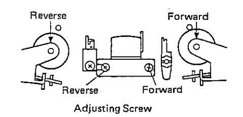
Figure 14-1 PINCH ROLLER PRESSURE AND AZIMUTH POINTS
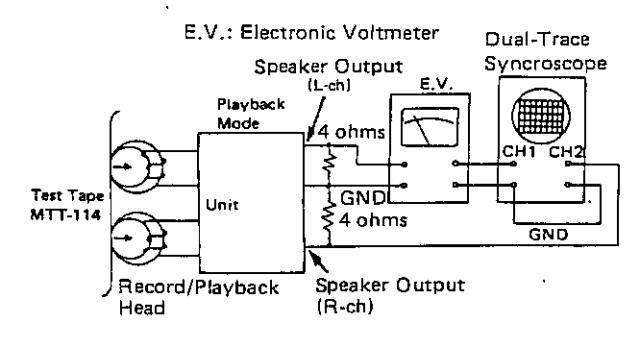


Figure 14-3 TAPE SPEED
TEST TAPES FOR MEASUREMENT
COMPACT CASSETTE TYPE
and then the forward playback screw.
| TITLE | MODEL | APPLICATION | |
|---|---|---|---|
| FLUTTER | MTT-111 | 3 kHz,10 dB |
Tape speed,
Wow and flutter check |
| AZIMUTH |
MTT-113
MTT-113C MTT-114 |
6.3 kHz, —10 dB
8 kHz, —10 dB 10 kHz, —10 dB |
Head azimuth
adjustment |
| DISTORTION | MTT-118 | 1 kHz, —10 dB |
Distortion check
level adjustment |
|
DOLBY LEVEL
CALIBRATION |
MTT-150 |
Dolby B-Type
Tone 200 nwb/m |
Dolby NR
B-type level adjustment |
| BLANK | MTT-502 |
Record fre-
quency check |
TORQUE METER FOR COMPACT CASSETTE
| MODEL |
MEASUREMENT
RANGE |
APPLICATION |
|---|---|---|
| TW-2111 | 10 – 100 g-cm | Normai : Playback torque |
| 1.5 — 10 g-cm | Normal : Back-tension | |
| TW-2121 | 10 100 g-cm | Reverse : Playback torque |
| 1.5 — 10 g-cm | Reverse : Back-tension | |
| TW-2231 | 30 – 200 g-cm | Fast-forward, Rewind torque |
| TW-2412 | 0 — 300 g | Normal : Driving power |
| TW-2422 | 0 300 g | Reverse : Driving power |
-- 14 --

MECHANISCHE EINSTELLUNG
|
BÉ-
NENNUNG |
VER-
WENDETES MESSGERÄT |
EINSTELL-
PUNKT |
BEMERKUNGEN
(PRÛFUNG) |
|---|---|---|---|
|
Andruck-
rollen- druck |
Federwaage
(500 g) |
Andruckrollen-
druckfeder |
300 – 420 g
* Wenn ein anderer Wert angezeigt wird, die Druck- feder der Andruckrolle auswechseln. |
|
Antriabs-
kraft |
Bandzug
Meßcassette Vorwarts TW-2412 Gegenrichtung TW-2422 |
Mehr als 130 y | |
|
Dreh-
moment |
Drehmoment-
messer Wiedergabe, Vorwärts: TW-2111 Wiedergabe, Gegenrichtung: TW-2121 Schnellvorlauf: TW-2231 Rückspulung: TW-2231 |
(Wiedergabe,
Vorwärts: 35 – 60 g-cm) (Wiedergabe Gegenrichtung: 35 – 60 g-cm) (Schnellvorlauf: 85 – 125 g-cm) (Rückspulung: 85 – 125 g-cm) |
|
| Azimut |
Testband
MTT-114 |
Azimuteinstell-
schraube *1 |
Sinuswellenform
wird maximal. |
|
Bandge-
schwin- digkeit |
Testband
MTT-111 |
3000
+ 105
Hz
_75 Hz |
*1 Um die Azimuteistellung durchzuführen zuerst die Bandumkehrwiedergabeschraube und dann die Voralufwiederoabeschraube einstellen.
TESTBÄNDER FÜR MESSUNG KOMPAKTCASSETTENTYP
| BENENNUNG | MODELL |
FREQUENZ/
PEGEL |
ANWENDUNG |
|---|---|---|---|
|
GLEICHLAUF-
SCHWAN- KUNGEN |
MTT-111 | 3 kHz, —10 dB |
Überprüfung der
Bandgesch- windigkeit und Gleichlauf- schwankungen |
| AZIMUT |
MTT-113
MTT-113C MTT-114 |
6,3 kHz, —10 dB
8 kHz, —10 dB 10 kHz,—10 dB |
Kopfazimutein-
stellung |
|
KLIRR-
FAKTOR |
MTT-118 | 1 kHz, —10 dB |
Verzerrungs-
pegeleinstellung |
|
DOLBY-
PEGEL- EICHUNG |
MTT-150 |
Ton von Dolby
B-Typ 200 nwb/m |
Dolby-NR B-
Typ-Pegelein- stellung |
|
LEER-
CASSETTE |
MTT-502 |
Überprüfung
der Aufnahme- frequenz |
DREHMOMENTMESSER FÜR KOMPAKTCASSETTE
| MODELL | MESSBEREICH | ANWENDUNG |
|---|---|---|
| TW-2111 | 10 100 g-cm | Normal : Wiedergabedrehmoment |
| 1,5 — 10 g-cm | Normal : Rückzug | |
| TW-2121 | 10 — 100 g-cm | Rücklauf : Wiedergabedrehmoment |
| 1,5 — 10 g-cm | Rücklauf : Rückzug | |
| TW-2231 | 30 — 200 g-cm |
Schneilvorlauf-, Rückspul-
drehmoment |
| TW-2412 | 0 — 300 g | Normal : Antriebskraft |
| TW-2422 | 0 — 300 g | Rücklauf : Antriebskraft |
RÉGLAGE DE MÉCANISME (F)
| ARTICLE | GABARIT |
POINTS DE
RÉGLAGE |
REMARQUES
(VERIFICATION) |
|---|---|---|---|
|
Pression
du ġalet pinceur |
Jauge de
tension (500 g) |
Ressort de
pression du galet pinceur |
300 – 420 g
* Si l'indication par la jauge est hors de la gamme, remplacer le ressort de pression du galet pinceur, |
|
Puissance
d'entraine- ment |
Cassette de
mesure de tension de la bande Avance TW-2412 Retour TW-2422 |
Ptus de 130 g | |
| Couple |
Compteur
de couple Lecture, Avance: TW-2111 Lecture, Retour: TW-2121 Avance rapide: TW-2231 Rebobinage: TW-2231 |
(Lecture, Avance:
35 à 60 g-cm) {Lecture, Ratour: 35 à 60 g-cm} (Avance rapide: 85 à 125 g-cm) (Rebobinage: 85 à 125 g-cm) |
|
| Azimut |
Bande d'essai
MTT-114 |
Vis de réglage
de l'azimut *1 |
La forme d'onde
sinusoïdale atteint |
|
Vitesse de
la bande |
Bande d'essai
MTT-111 |
3000 + 105
-75 Hz |
*1 Pour effectuer le réglage d'azimut aiuster d'abord la vis de lecture en retour et puis la vis de lecture d'avance.
BANDES D'ESSAI POUR MESURAGE TYPE CASSETTE COMPACTE
| TITRE | MODÈLE |
FRÉQUENCE/
NIVEAU |
APPLICATION |
|---|---|---|---|
| PLEURAGE | MTT-111 | 3 kHz, —10 dB |
Vérification de
la vitesse de bande et du pleurage et scintillement |
| AZIMUT |
MTT-113
MTT-113C MTT-114 |
6,3 kHz, —10 dB
8 kHz, —10 dB 10 kHz, —10 dB |
Réglage de
l'azimut de la tête |
| DISTORSION | MTT-118 | 1 kHz,10 dB |
Réglage de
niveau de distorsion |
|
CALIBRAGE
DU NIVEAU DOLBY |
MTT-150 |
Tonalité Dolby
type B, 200 nwb/m |
Réglage du
niveau type B Dolby NR |
|
ESPACE
VIERGE |
MTT-502 |
Vérification de
la fréquence d'enregistrement |
JAUGE DE COUPLE POUR CASSETTE COMPACTE
| MODÈLE |
GAMME DE
MESURE |
APPLICATION |
|---|---|---|
| TW-2111 | 10 — 100 g-cm | Normal : Lecture d'enroulement |
| 1,5 — 10 g-cm | Normal : Tension arrière | |
| TW-2121 | 10 – 100 g-cm | Retour : Lecture d'enroulement |
| 1,5 — 10 g-cm | Retour : Tension arrière | |
| TW-2231 | 30 — 200 g-cm |
Couple d'avance rapide et de
rebobinage |
| TW-2412 | 0 — 300 g | Normal : Puissance d'entrainement |
| TW-2422 | 0 - 300 g | Retour : Puissance d'entraînement |
CIRCUIT ADJUSTMENT (TUNER SECTION)
CLOCK REFERENCE FREQUENCY ADJUSTMENT
Set the receiving frequency band to FM.
(F
| FREQUENCY DISPLAY | ADJUSTMENT | REMARKS |
|---|---|---|
| 108.0 MHz | TC801 | 118.7 MHz ±2kHz |
FM IF AND FM SIGNAL DETECTOR OUTPUT VOLTAGE ADJUSTMENT
| • | |||||
|---|---|---|---|---|---|
|
SWITC
POSIT |
CH
TON |
FM mono | |||
|
SIGNA
GENE |
RATOR | 1 kHz, 30%, FM modulated | |||
| STEP |
TEST
STAGE |
FRE-
QUENCY |
FRE-
QUENCY DISPLAY |
ADJUST-
MENT |
REMARKS |
| 1 |
IF/FM
SD Output |
98.0 MHz
at 54 dB |
98.0 MHz | τ1 |
Adjust for
minimum output, |
|
SIGNA
GENE |
RATOR | 400 Hz, 22.5 kHz dev, FM modulated | lated | ||
| 2 | IF |
98.0 MHz 98.0 MHz T2 Adjust for
at 10 dB maximal output. |
|||
FM STEREO SEPARATION ADJUSTMENT
|
SWITCH
POSITION |
FM stereo | FM stereo | ||
|---|---|---|---|---|
|
SIGNAL
GENERATOR |
400 Hz, 22.5 | 400 Hz, 22.5 kHz dev, FM modulated | ||
| FREQUENCY |
FREQUENCY
DISPLAY |
ADJUSTMENT | REMARKS | |
| 98.0 MHz 74 dB | 98.0 MHz |
VR201
(Fig.18-2) |
Adjust for maxi-
mal separation. |
|
VCO FREQUENCY ADJUSTMENT
|
SIGNAL
GENERATOR |
400 Hz, 22.5 kHz dev, FM modulated
(mono signal) |
|||
|---|---|---|---|---|
| FREQUENCY |
FRE- ADJUST- REMARKS
QUENCY MENT DISPLAY |
|||
| FM mono position |
FM stereo |
(unmodula |
position
ted) |
||
| 98.0 MHz at 60 dB | 98.0 MHz |
VR202
(Fig.182) |
Adjust for 19.00 kHz
±50 Hz. |
|
ANSS ADJUSTMENT
|
SWITCH
POSITION |
FM ma | FM mono | ||
|---|---|---|---|---|
|
SIGNAL
GENERATOR |
400 Hz, 22.5 kHz dev, FM modulated | ulated | ||
| FREQUENCY | NCY | ADJUSTMENT | REMARKS | |
| 19 kHz | 108,0 MH | z | L51 |
Adjust for mini-
mum output. |
| LCD PWB | ТСВ | 01 | ||
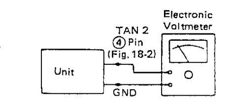
Figure 16-1 CLOCK REFERENCE FREQUENCY

Figure 16-2 IF/FM SD OUTPUT


Figure 16-4 VCO/ANSS

Figure 16-5 ADJUSTMENT POINTS

SCHALTUNGSEINSTELLUNG (TUNERTEIL)
ABGLEICH DER UHRENBEZUGSFREQUENZ Die Empfangsfrequenz auf das UKW einstellen.
| FREQUENZANZEIGE | EINSTELLUNG | BEMERKUNGEN | ||
|---|---|---|---|---|
| 108,0 MHz | TC801 | 118,7 MHz ±2 kHz | ||
AUSGANGSSPANNUNGSABSTIMMUNG FÜR UKW-ZF-UND UKW-SIGNALDETEKTOR
| SCHA | UKW-Wellenband | |||||
|---|---|---|---|---|---|---|
|
SIGNA
GENE |
L-
RATOR |
1 kHz, 30%, UKW-Modulation | ||||
|
SCH-
RITT |
PRÜF-
STUFE |
FRE- FREQUENZ-EINSTEL-
QUENZ ANZEIGE LUNG |
BEMER-
KUNGEN |
|||
| 1 |
ZF/UKW-
SD- Ausgang |
98,0 MHz
bei 54 dB |
98,0 MHz | Т1 |
Den kern Auf
minimum Ausgang ein- stellen. |
|
|
SIGNA
GENEI |
400 Hz, 2 | 2,5 kHz Hub | , UKW-Mo | dulation | ||
| 2 | ZF |
98,0 MHz
bei 10 dB |
98,0 MHz | Т2 |
Auf maxi-
malen Aus- gang ein- stellen |
|
EINSTELLUNG DER UKW-TRENNUNG
|
SCHALTER-
STELLUNG |
FM stereo | FM stereo | ||||
|---|---|---|---|---|---|---|
|
SIGNAL-
GENERATOR |
400 Hz, 22,5 k | 400 Hz, 22,5 kHz Hub, UKW-Modulation | ||||
| FREQUENZ |
FREQUENZ-
ANZEIGE |
EINSTEL-
LUNG |
BEMER-
KUNGEN |
|||
|
98,0 MHz
74 dB |
98,0 MHz |
VR201
(Abb. 182) |
Auf Maximalen
Trennung ein- stellen, |
|||
EINSTELLUNG DER VCO-FREQUENZ
| SIGNAL- | 400 Hz, 22,5 k | 400 Hz, 22,5 kHz Hub, UKW-Modulation | |||
|---|---|---|---|---|---|
| GENERATOR | (Mono-Signal) | (Mono-Signal) | |||
| FREQUENZ |
FREQUENZ-
ANZEIGE |
EINSTEL-
LUNG |
BEMERKUNGEN | ||
| FM mono-Positio | n |
FM stereo-Position
(unmoduliert) |
|||
| 98,0 MHz bei | 98,0 MHz | VR202 | Auf 19,00 kHz ± | ||
| 60 dB | (Abb. 18–2) | 50 Hz einstellen. | |||
ANSS-EINSTELLUNG
|
SCHALTER-
STELLUNG |
FM mono | FM mono | ||||
|---|---|---|---|---|---|---|
|
SIGNAL-
GENERATOR |
400 Hz, 22,5 k | 400 Hz, 22,5 kHz Hub, UKW-Modulation | ||||
| FREQUENZ |
FREQUENZ-
ANZEIGE |
EINSTEL- |
BEMER-
KUNGEN |
|||
| 19 kHz | 108,0 MHz | L51 |
Den kern Auf
minimum Ausgang ein- stellen. |
|||
F RÉGLAGE DU CIRCUIT (SECTION DU TUNER)
RÉGLAGE DE LA FREQUENCE DE REFERENCE DE LA MONTRE
Régler la gamme de fréquence de réception sur FM.
|
AFFICHAGE DE
FRÉQUENCE |
RÉGLAGE | REMARQUES |
|---|---|---|
| 108,0 MHz | TC801 | 118,7 MHz ±2 kHz |
RG-F851G
RÉGLAGE DE LA TENSION DE SORTIE DU DÉTECTEUR DE SIGNAL FM ET DE FI FM
|
POSITI
COMM |
ON DU
UTATEUR |
FM Mono | ||||
|---|---|---|---|---|---|---|
|
GÉNÉF
DE SIG |
IATEUR
NAUX |
1 kHz, 30%, modulė FM | ||||
|
ÉTAPE ÉTAGE
D'ESSAI |
FRÉ-
QUENCE |
AFFICHAGE
DE FRÉ- QUENCE |
RÉGLAGE | REMARQUES | ||
| 1 |
Sortie SD
FI/FM |
98,0 MHz
à 54 dB |
98,0 MHz | Τ1 | Régler sur la sortie minimale. | |
|
GÉNÉF
DE SIG |
400 Hz, d | év. de 22,5 kł | ⊣z, modulé | FM | ||
| 2 | Fi |
98,0 MHz
à 10 dB |
98,0 MHz | T2 |
Régler sur la
sortie maxi- male, |
|
RÉGLAGE DE LA SÉPARATION FM STÉRÉO
| POSITION DU | FM stéréo | ||||
|---|---|---|---|---|---|
|
GÉNÉRATEUR
DE SIGNAUX |
400 Hz, dév. d | 400 Hz, dév. de 22,5 kHz, modulé FM | |||
| FRÉQUENCE |
AFFICHAGE
DE FRÉ- QUENCE |
RÉGLAGE | REMARQUES | ||
|
98,0 MHz
74 dB |
98,0 MHz |
VR201
(Fig. 18–2) |
Régier pour
que la sépara- tion soit maxi- male. |
||
RÉGLAGE DE LA FRÉQUENCE VCO
|
GÉNÉRATEUR DE
SIGNAUX |
400 Hz, dév. de 22,5 kHz, modulé FM
(mono signal) |
|||
|---|---|---|---|---|
| FRÉQUENCE |
AFFICHAGE
DE FREQUENCE |
RÉGLAGE | REMARQUES | |
| Position FM mono |
Position FM stéréo
(non modulés) |
|||
|
98,0 MHz à
60 dB |
98,0 MHz |
VR202
{Fig. 18–2} |
Réglage sur
19,00 kHz ± 50 Hz. |
|
RÉGLAGE DE L'ANSS
| POSITION DU | R FM mono | ||
|---|---|---|---|
|
GÉNÉRATEUR
DE SIGNAUX |
400 Hz, dév. | de 22,5 kHz, mo | dulé FM |
| FRÉQUENCE |
AFFICHAGE
DE FRÉ- QUENCE |
RÉGLAGE | REMARQUES |
| 19 kHz | 108,0 MHz | L51 | Régler sur la sortie minimale. |
(E)
AUTO NOISE CUT LEVEL ADJUSTMENT
|
SWITCH
POSITION |
FM mono | |||
|---|---|---|---|---|
|
SIGNAL
GENERAT |
DR | 6.3 kHz, 30 %, FM modulated = 0 dB | ||
|
FRE-
QUENCY |
FRE-
DUENCY DISPL |
ADJUST-
MENT |
REMARKS | |
|
98.0 MHž
50 dB |
98.0 1 | ИНz | VR1 |
Adjust VR1 so that the out-
put is changed from 0 dB to 3 dB when the input is reduced from 74 dB to 45 dB. |
Figure 18-1 AUTO NOISE CUT LEVEL
D
PEGELEINSTELLUNG DER AUTOMATISCHEN RAUSCHUNTERDRÜCKUNG
|
SCHALTER-
STELLUNG UKW-Wellenband |
] | |||||||
|---|---|---|---|---|---|---|---|---|
|
SIGNAL-
GENERAT |
OR ( | 5,3 kHz, 30%, m | odulé FM ≈ 0 dB | ] Co | llector | TANO | I | C201 63. |
|
FRE-
QUENZ |
FRE-
QUENZ ZEIGE |
AN EINSTEL- |
BEMER-
KUNGEN |
I | ||||
|
98,0 MHz
50 dB |
98,0 MF | lz VR1 |
VR1 so einstellen, daß der
Ausgang von 0 dB auf –3 dB geändert wird, wenn der Ein- gang von 74 dB auf 45 dB reduziert. |
:
- - , I |
||||
F
RÉGLAGE DU NIVEAU DE COUPURE AUTOMATIQUE DE BRUITS
|
POSITION
COMMUT |
FM m | FM mone | |||
|---|---|---|---|---|---|
|
GÉNÉRATEUR
DE SIGNAUX |
6,3 kHz, 30%, modulé FM = 0 dB | ||||
|
FRÉ-
QUENCE |
AFFICHAGE
DE FRÉQUENCE |
RÉGLAGE | REMARQUES | ||
|
98,0 MHz
50 dB |
98,0 Mi | Ηz | VR1 |
Régler VR1 de telle sorte que
la sortie passe de 0 dB à3 dB lorsque l'entrée est réduite de 74 dB à 45 dB. |
|

-
Garrie Booteds (
Figure 18-2 ADJUSTMENT POINTS
- 18 -

MW/IW IF/BF ADJUSTMENT
|
SI
GEN |
GNAL
ERATOR |
400 Hz, 309 | %, AM mod | ulated | ||
|---|---|---|---|---|---|---|
| STEP |
TEST
STAGE |
FRE-
QUENCY DISPLAY |
ADJUST-
MENT |
REMARKS | ||
| MW/LV | V IF (Set the | receiving fr | equency bar | nd to MW.) | ||
| 1 | IF | 450 kHz | 522 kHz |
T101
T102 |
Adjust for
best ".1F" curve. |
|
| MW RF | ||||||
| 2 | Band | No signal | 522 kHz | L106 | 1.2 V | |
| 3 | coverage | is used. | 1,620 kHz | TC103 | 8.0 V | |
| 4 |
Repeat ster
made. |
ps 2 and 3 u | ntil no furth | er improver | nent can be | |
| 5 | Tracking | 600 kHz | 600 kHz |
L102
L104 |
Adjust for
maximal |
|
| 6 | 1,400 kHz | 1,400 kHz |
TC101
TC102 |
output. | ||
| 7 |
Repeat ste
made |
ps 5 and 6 u | ntil no furth | ier improve | ment can be | |
| (Set the rec | eiving frequ | ency band to | o LW.) | |||
| 8 | Band | No signal | 153 kHz | L107 | 2.7 V | |
| 9 | COVEIBUE | is used. | 281 kHz | TC104 | 7.1 V | |
| 10 |
Repeat ste
made. |
ps 8 and 9 u | ntil no furth | er improve | ment can be | |
| 11 | Tracking | 160 kHz | 160 kHz | L103 | Adjust for | |
| 12 | 270 kHz | 270 kHz | L105 |
maximal
output. |
||
| 13 |
Repeat ste
be made. |
eps 11 and 11 | 2 until no fu | rther impro | vement can | |
Note: Perform the Band coverage adjustment for MW prior to the one for LW, and carry out the tracking for LW prior to that for MW.
MW SIGNAL LEVEL ADJUSTMENT
|
SIGNAL
GENERATOR |
54 dB, Unr | 54 dB, Unmodulated | ||||
|---|---|---|---|---|---|---|
| FREQUENCY |
FRE-
QUENCY DISPLAY |
ADJUST-
MENT |
REMARKS | |||
| 999 kHz | 999 kHz | VR151 | 4 ± 0,1∨ | |||

RG-F851G
Figure 19-1 AM "IF" CURVE


Figure 19-3 ADJUSTMENT POINTS
MW/LW-ZF/HF EINSTELLUNG
|
SIC
GENI |
SNAL- | 400 Hz, 30 | % , AM-Modi | ulation | |
|---|---|---|---|---|---|
|
SCH-
RITT |
PRÜF-
STUFE |
FRE-
QUENZ |
FRE-
QUENZAN- ZEIGE |
EINSTEL-
LUNG |
BEMER-
KUNGEN |
| MW/LW | ZF (Die Em | pfangsfreque | nz auf das MV | V-Wellenband | einstellen.) |
| 1 | ZF | 450 kHz | 522 kHz |
T101
T102 |
Auf beste
ZF-Kurve einstellen. |
| MW HF | |||||
| 2 | _ | Kein Sig- | 522 kHz | L106 | 1,2 V |
| 3 |
Frequenz-
bereich |
rator wird
verwendet. |
1620 kHz | TC103 | 8,0 V |
| 4 |
Die Schritt
Verbesseru |
te 2 und 3 w
ing möglich |
/iderholen, b
ist. |
is keine weit | ere |
| 5 | Gleichlauf | 600 kHz | 600 kHz | L102,L104 |
Auf maxi-
malen Aus- |
| 6 | 1400 kHz | 1400 kHz |
TC101
TC102 |
gang ein-
stellen. |
|
| 7 |
Die Schrit
Verbesseru |
te 5 und 6 v
Ing möglich |
viederholen,
ist. |
bis keine we | itere |
| LW HF | (Die Empfa | ngsfrequenz | auf das LW | Wellenband | einstellen.) |
| 8 | Frequenz- |
Kein
Signal- |
153 kHz | L107 | 2,7 V |
| 9 | bereich |
generator
wird ver- wendet. |
281 kHz | TC104 | 7,1 V |
| 10 |
Die Schrit
Verbesser |
te 8 und 9 v
ung möglich |
viederholen,
ist. |
bis keine we | itere |
| 11 | Gleich- | 160 kHz | 160 kHz | L103 | Auf maxi- |
| 12 | lauf | 270 kHz | 270 kHz | L105 |
maien Aus-
gang ein- stellen. |
| 13 |
Die Schrit
Verbesser |
te 11 und 1
ung möglich |
2 wiederhole
ist. |
n, bis keine | weitere |
Anmerkung: Die Frequenzbereich-Einstellung für das MW-Wellenband muß vor der Einstellung des LW-Bereiches vorgenommen werden. Die Abtastung für LW sollte vor der Einstellung für MW ausgeführt werden.
MW-SIGNALBSTIMMUNG
|
SIGNAL-
GENERATOR |
54 dB, Unm | 54 dB, Unmoduliert | ||||
|---|---|---|---|---|---|---|
| FREQUENZ |
FRE-
QUENZ- ANZEIGE |
EINSTEL-
LUNG |
BEMERKUNGEN | |||
| 999 kHz | 999 kHz | VR151 | 4 ± 0,1 V | |||
F
RÉGLAGE DE FI/RF PO/GO
|
GÉNÉ
DE SI |
RATEUR
GNAUX |
400 Hz, 30 | ) %, modulé | AM | |
|---|---|---|---|---|---|
| ÉTAPE |
ÉTAGE
D'ESSAI |
FRÉ-
QUENCE |
AFFICHA
GE DE FRÉ- QUENCE |
RÉGLAGE | REMARQUES |
| FI PO/C | GO (Régler la | a gamme de | fréquence o | le réception | sur PO.) |
| 1 | FI | 450 kHz | 522 kHz |
T101
T102 |
Régier sur la
meilleure courbe "F1". |
| RF PO | |||||
| 2 | Couverture | Pas de | 522 kHz | L106 | 1,2 V |
| 3 |
de gamme
d'ondes |
gene-
rateur de signaux utilisé. |
1620 kHz | тс103 | 8,0∨ |
| 4 |
Refaire les
ultérieure |
étapes 2 et
ne puisse pl |
3 jusqu'à ce
us être obte |
e qu'une ame
nue. |
ilioration |
| 5 | Alianomont | 600 kHz | 600 kHz |
L102
L104 |
Régler sur la sortie maxi- |
| 6 | Alignement | 1400 kHz | 1400 kHz |
TC101
TC102 |
male. |
| 7 |
Refaire les
ultérieure |
étapes 5 et
ne puisse p |
t 6 jusqu'à ce
lus être obte |
e qu'une am
nue. |
élioration |
| RF GO | (Régler la g | amme de f | réquence de | réception su | ır GO.) |
| 8 | Couverture | Pas de | 153 kHz | L107 | 2,7 ∨ |
| 9 | d'ondes |
rateur de
signaux utilisé. |
281 kHz | TC104 | 7,1 V |
| 10 |
Refaire les
ultérieure |
étapes 8 e
ne puisse p |
t 9 jusqu'à c
lus être obte |
e qu'une am
inue. |
élioration |
| 11 | Alignemen | 160 kHz | 160 kHz | L103 | Régler sur la |
| 12 | 1 | 270 kHz | 270 kHz | L105 |
sortie maxi-
male. |
| 13 |
Refaire les
ultérieure |
s étapes 11
ne puisse p |
et 12 jusqu'a
lus être obte |
à ce qu'une :
inue. |
amélioration |
Note: Effectuer le réglage de Couverture de gamme d'ondes pour PO avant celui de GO; et effectuer le pistage de GO avant celui de PO.
RÉGLAGE DU NIVEAU DE SIGNAL PO
|
GÉNÉRATEUR
DE SIGNAUX |
54 dB, Non modulés | ||||
|---|---|---|---|---|---|
| FRÉQUENCE |
AFFICHAGE
DE FRÉQUENCE |
RÉGLAGE | REMARQUES | ||
| 999 kHz | 999 kHz | VR151 | 4 ± 0,1 ∨ | ||

.
-----

NOTES ON SCHEMATIC DIAGRAM
Besistor:
(F)
To differentiate the units of resistors, such symbol as K and M are used: the symbol K means 1000 ohm and the symbol M means 1000 kohm and resistor without any symbol is ohm-type resistor.
Capacitor:
To indicate the unit of capacitor, a symbol P is used: this symbol P means micro-micro-farad and the unit of the capacitor without such a symbol is microfarad. As to electrolytic capacitor, the expression "capacitance/withstand voltage" is used.
The indicated voltage in each section is the one measured by Digital Multimeter between such a section and the chassis with no signal given.
-
Schematic diagram and Wiring Side of P.W.Board for this model are subject to change for improvement without prior notice.
ANMERKUNGEN ZUM SCHEMATISCHEN SCHALTPLAN
• Widerstände:
Um die Einheiten der Widerstände unterscheiden zu können, werden Symbole wie K und M benutzt. Das Symbol K bedeutet 1000 Ohm und das Symbol M 1000 Kiloohm. Bei Widerständen ohne Symbol handelt es sich um ohmsche Widerstände.
Kondensatoren:
Zum Bezeichnen der Kondensatoreinheit wird das Symbol P benutzt; dieses Symbol P bedeutet Nanofarad. Die Einheit eines Kondensators ohne Symbol ist Mikrofarad. Für Elektrolytkondensatoren wird die Bezeichnung "Kapazität / Stehspannung" benutzt.
Die in den einzelnen Teilen angegebenen Spannungen werden mit einem Digitalvielfachmeßgerät zwischen dem betreffenden Teil und dem Chassis ohne Signalzuleitung gemessen.
Änderungen des schematischen Schaltplans und der Verdrahtungsseite der Leiterplatte f ür dieses Modell im Sinne von Verbesserungen jederzeit vorbehalten.
REMARQUES CONCERNANT LE DIAGRAMME SCHÉMATIQUE
Résistance:
Pour différencier les unités de résistances, on utilise des symbole tels que K et M: le symbole K signifie 1000 ohms, le symbole M signifie 1000 kohms et la résistance donnée sans symbole est une résistance de type ohm.
Condensateur:
Pour indiquer l'unité de condensateur, on utilise le symbole P; ce symbole P signifie micro-microfarad, et l'unité de condensateur donnée sans ce symbole est le microfarad. En ce qui concerne le condensateur électrolytique, on utilise l'expression "tension de régime/capacité"
La tension indiquée dans chaque section est celle mesurée par un multimètre numérique entre la section en question et le châssis, en l'absence de tout signal.
Le diagramme schématique et le côté câblage de la PMI de ce modèle sont sujets à modifications sans préavis pour l'amélioration de ce produit.


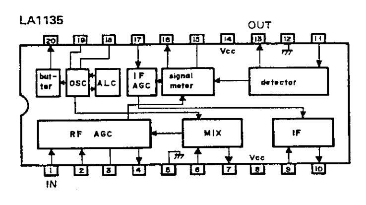


Figure 30 EQUIVALENT CIRCUIT (BLOCK DIAGRAM) OF IC


Lun -ol


- 31 -
|
E
REPLACEMENT PARTS LIST |
F
LISTE D DE RE |
|
|---|---|---|
|
"HOW TO ORDER REPLACEMENT
PARTS" |
"BESTELLEN VON ERSATZTEILEN" |
"COMMENT
PIÈCES DI |
|
To have your order filled promptly and
correctly, please furnish the following information. 1. MODEL NUMBER 2. REF. NO. 3. PART NO. 4. DESCRIPTION |
Um Ihren Auftrag schnell und richtig
ausfuhren zu können, bitten wir um die folgenden Angaben, 1. MODELLNUMMER 2. REF. NR. 3. TEIL NR. 4. BESCHREIBUNG |
Pour voir votre r
manière rapide e nir les renseign 1. NUMÉ 2. N° DE 3. N° DE 4. DESCI |
| REF.NO. PART NO. D | ESCRIPTION CODE REF.NO. | PART NO. |
DC - E951C
| INTEGRATI | ED CIRCUITS |
D201
D501 |
VHD1$$119//-1
VHD1$$119//-1 |
Silico
Silico |
||
|---|---|---|---|---|---|---|
| AK | D502 | VHD15S119//-1 | Silico | |||
| C1 | VH10PC1245V-1 | FIVE IF, μPC1245V | D502 | VHD1SS119//-1 | Silico | |
| C51 | RH-IX111UAFZZ | ANSS, HALIZIS | D503 | VHD1SS119//-1 | Silicor | |
| C1 01 | VHILA1135//-1 | AM IF Amp., LAI 135 | D504 | VHD155119//-1 | Silicor | |
| C201 | VHIBA1355//-1 | PLL FM MPX, BA1355 | AG | Silico | ||
| C401 | VHIUPC1228HA1 | Pre Amp., µPC1228HA | AE | 0552 | VHD155119//-1 |
Silico
Cili |
| C701 | VHiHA1377//1F | Power Amp., HA1377 | АК | 0555 | VHUISSII9//-I | Shico |
| C801 | RH-IX1306AFZZ | Microcomputer | АХ | D557 | VHD155119//-1 | Sincor |
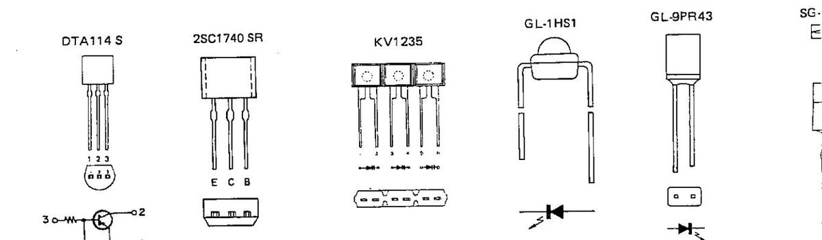
| TRAN | SISTORS | i | D561 | VHERDI TOEB3-1 | Zener | |
| 111-01 | D562 | VHD1SS119//-1 | Silico | |||
| 11 | VS2SC535-C/-1 | Silicon, NPN, 2SC535 C | AC | D563 | VHERD5 R6JS2-1 | Zener |
| 12 | VS2SC1740SR-1 | Silicon, NPN, 2SC1740 SR | AB | D564 | VHD11E1TA2/-1 | Silico |
| 211 | VSDTC114S//-1 | Digital Transistor, DTC114 S | AB | D565 | VHD11E1TA2/-1 | Silicor |
| 251 | VS2SC2603-F-1 | Silicon, NPN, 2SC2603 F | AB | D701 | VHD1SS119//-1 | Silico |
| 0101 | VS2SC1740SR-1 | Silicon, NPN, 2SC1740 SR | AB | D702 | VHD1SS119//-1 | Silico |
| 102 | VS2SK184BL/-1 | FET. 2SK184 BL | AC | D801/802 | VHD1 SS184//-1 | Silico |
| 0103 | VS2SC535-C/-1 | Silicon, NPN, 2SC535 C | AC | D803 | VHD1 SS193//-1 | Silicor |
| 100 | VS2SC535-C/-1 | Silicon NPN 2SC535 C | AC | D805 | VHD1 SS193//-1 | Silico |
| 104 | VS2SC535-C/-1 | Silicon NPN 2SC535 C | AC | 851 C | ||
| 105 | VS250535-0/-1 | Silicon NPN 2SC535 C | AC | D805/806 | VHD1 SS184//-1 | Silicor. |
| 108 | V3230335-C/-1 | Silicon NPN 250535 C | AC | 852E | ||
| 2107 | V626C17406P 1 | Silicon, NPN 2501740 SB | ΔR | D807/808 | VHD1 SS184//-1 | Silico: |
| Silison NEN 2SCE35 C | D809/810 | VHD1 SS184//-1 | Silico | |||
| 1109 | VS25C535-C/-1 | Silicon, NFN, 230333 C | D811/812 | VHD1SS184//-1 | Silicor | |
| 1151 | VS25017405R-1 | SHICON, NPN, 23CI 740 SH | VHPG19PB43/-1 | |||
| 2152 | VS25017405R-1 | Silicon, NPN, 23C1740 SR | VHPSG263D//-1 | |||
| 2153 | VS2SC1740SR-1 | Silicon, NPN, ZSCI 740 Sh | LEDUST | |||
| 2154 | VS2SC1740SR-1 | Silicon, NPN, 2SCI 740 SR | AB | |||
| 2201 | VS2SC1740SR-1 | Silicon, NPN, 2SC1 /40 SR | AB | LED851 | ||
| 2501 | VS2SC1740SR-1 | Silicon, NPN, 2SCI 740 SR | AB | LED852 | ||
| 2551 | VSDTC114S//-1 | Digital Transistor, DTC114 S | AB | LED853 | VHPGLIHSIUI-I | |
| 2552 | VSDTC1145//-1 | Digital Transistor, DTC114 S | AB | LED854 | VHPGLIHSIUI-I | |
| 2561 | VS2SD1406Y/-1 | Silicon, NPN, 2SD1406 Y | AE | LED855 | VHPGL1HS101-1 | LED, C |
| 2562 | VS2SC22366/-1 | Silicon, NPN, 2SC2236 O | AC | LED856 | VHPGL1HS101-1 | LED, C |
| 2563 | VSDTC114S//-1 | Digital Transistor, DTC114 S | AB | LED857 | VHPGL1HS101-1 | LED, C |
| 2564 | VS2SA933-R/-1 | Silicon, PNP, 2SA933 R | AC | LED858 | VHPGL1HS101-1 | LED, C |
| 2565 | VSDTC114S//-1 | Digital Transistor, DTC114 S | AB | LED859 | VHPGL1 HS101-1 | LED, O |
| 2566 | VS2SA933-R/-1 | Silicon, PNP, 2SA933 R | AC | VC101 | VHCKV1235Z2-1 | Varicar |
| 0701 | VS2SD655E//-1 | Silicon, NPN, 2SD655 E | AC | VC102 | VHCKV1235Z2-1 | Varica; |
| 0702 | VS2SD655E//-1 | Silicon, NPN, 2SD655 E | AC | VC103 | VHCKV1235Z2-1 | Varicap |
| 0801 | VSDTA114S//-1 | Digital Transistor, DTA114 S | AB | · | ||
| 1807 | VSDTC1145//-1 | Digital Transistor, DTC114 S | AB | FI | LTERS | |
| 0002 | V$2541162Y/-1 | Silicon PNP 2SA1162 Y | AB | |||
| 4004 | V323A(1021/-1 | Chip Type | , | CF1 | RFiLF0079AFZZ | FM IF |
| 0805 | VS2SA1162Y/-1 | Silicon, PNP, 2SA1162 Y, | AB | CF2 | RFILF0079AFZZ | FM IF |
| Chip Type | CF101 | RFiLA0103AFZZ | AM IF, | |||
| 0806 | VS2SA1162Y/-1 | Silicon, PNP, 2SA1162 Y, | AB | CF101 | RFiLA0117AFZZ | AM IF, |
| Chip Type | CF102 | RFiLA0119AFZZ | AM IF, | |||
| CF102 | RFiLA0118AFZZ | AM IF, | ||||
| DI | IODES | EMF551 | RFill0063AFZZ | Noise F | ||
| EMF552 | RFILLOO63AFZZ | Noise F | ||||
| D101 | VHD1SS119//-1 | Silicon, 1SS119 | AA | FIL100 | RFiLR0003AFZZ | Band P |
| D102 | VHD1 SS1 19//-1 | Silicon, 1SS119 | AA | I FIL101 | RFiLR0002AFZZ | Band P. |
RG-F851G RG-F852F
| REF.NO. | PART NO. | DESCRIPTION | CODE | |
|---|---|---|---|---|
| TRANS | FORMERS | |||
| T1 | RCILIO336AFZZ | FM IF | AE | |
| T2 | FM IF, Part of REF.NO.337 | |||
| T101 | RCILIO348AFZZ | AM IF, 851G | AC | |
| T101 | RCILIO352AFZZ | AM IF, 852E | AC | |
|
T102
T102 |
RCILIO334AFZZ | AM IF, 852E | AC | |
| . Co | DILS | |||
| L51 | RCiLZ0085AFZZ | 19 kHz, Trap | AE | |
| L100 | VP-DH2R2M0000 | 2.2 μH, Choke | AB | |
| L101 | VP-DH680K0000 | 68 μH, Choke | AB | |
| L102 | RCiLA0714AFZZ | MW Antenna | AC | |
| L103 | RCiLA0715AFZZ | LW Antenna | AC | |
| L104 | RCiLR0386AFZZ | MW RF | AC | |
| L105 | RCiLR0387AFZZ | LW RF | AC | |
| L106 | RCiLB0727AFZZ | MW Oscillation, 851G | AC | |
| L106 | RUILBU786AFZZ | AC | ||
| L107 | LW Oscillation, 851G | AC | ||
| 1108 | 180 µH Choke | AB | ||
| L550 | VP-CH331 K0000 | 330 μH, Choke | AB | |
| CON | TROLS | |||
| TC101 | RTō-H1072AFZZ | Trimmer, 20 pF | AC | |
| TC102 | RTō-H1072AFZZ | Trimmer, 20 pF | AC | |
| TC103 | RTö-H1072AFZZ | Trimmer, 20 pF | AC | |
| TC104 | RTō-H1069AFZZ | Trimmer, 60 pF | AD | |
| TC801 | RTō-H1101AFZZ | Trimmer, 20 pF | AD | |
| VR1 | RVR-M0432AFZZ | Volume, 10 kohm(B) | AB | |
| VR151 | RVR-M0433AFZZ | Volume, 20 kohms(B) | AB | |
| VH201 | Volume, 30 konms(B) | |||
| VRZUZ | Volume 50 kohms/0) × 2 | |||
| VR657 | RVR-00717AFZ2 | Volume, 50 kohms(W) | AD | |
| VR701 | RVR-Z0212AFZZ | Volume, 50 kohms(B) × 2 | AN | |
| with Switch × 2 | ||||
| THER | MISTOR | |||
| TH151 | VHH41 D26///1 F | 10 kohm, Temperatures | AB | |
| Detection | ||||
| ELECTROLYT | IC CAPACITORS | |||
| (All electrolytic | capacitors are 120% | (ypa.) | ||
| C6 | RC-EZY105AF1H | 1 μF, 50V | АВ | |
| C9 | RC-EZY474AF1 H | 0.47 μF, 50V | AB | |
| C13 | RC-EZY474AF1H | 0.47 μF. 50V | AB | |
| C20 | RC-EZY105AF1H | 1 μF, 50V | AB | |
| C59 | RC-EZY224AF1H | 0.22 μι, 50ν | ||
| C101 | RU-EZYIOZAFIH | |||
| C129 | RC-E7Y225AELH | 2.2 μE 50V | AB | |
| C130 | RC-EZY225AF1H | 2.2 μF, 50V | AB | |
| C131 | RC-EZY105AF1H | 1 μF, 50V | AB | |
| C153 | RC-EZ1316AFZZ | 10 μF, 16V | AB | |
| C203 | RC-EZD334AF1H | 0.33 µF, 50V | AB | |
| C205 | RC-EZD476AF1C | 47 μF, 16V | AB | |
| C207 | RC-EZD474AF1H | 0.47 μF, 50V | AB | |
| C208 | RC-EZD224AF1H | 0.22 μF, 50V | AB | |
| C209 | RC-EZD105AF1H |
ιμη, 50V
10 με 16V |
||
| C212 | RC-EZDIUGAFIU | 2.2 μF. 50V | AB | |
| C213 | RC-EZD225AF1H | 2.2 μF, 50V | AB |
RC-EZD474AF1H 0.47 μF, 50V
RC-EZD474AF1H 0.47 µF. 50V
C403
C404
| REF.NO. | PART NO. | DESCRIPTION | CODE |
|---|---|---|---|
| C405 | RC-EZD336AF1A | 33 μF, 10V | AB |
| C406 | RC-EZD336AF1A | 33 µF, 10V | AB |
| C503 | RC-EZD105AF1H | 1 μF, 50V | AB |
| C504 | RC-EZD105AF1H | 1 μF, 50V | AB |
| C505 | RC-EZD476AF1C | 47 μF, 16V | AB |
| C506 | RC-EZD106AF1C | 10 μF, 16V | A8 |
| C551 | RC-EZD106AF1C | 10 μF, 16V | AB |
| C552 | RC-EZD336AF1A | 33 μF, 10V | AB |
| C555 | RC-GZA227AF1C | 220 μF, 16V | AB |
| C556 | RC-GZA476AF1C | 47 μF, 16∨ | AB |
| C559 | RC-EZ4475AF1E | 4.7 μF, 25V | АБ |
| C563 | RC-GZA476AF1C | 47 μF, 16V | AB |
| C570 | RC-EZS475AF1E | 4.7 μF, 25V | AB |
| C705 | RC-EZD106AF1C | 10 μF, 16V | AB |
| C706 | RC-GZV108AF1C | 1000 μF. 16V | AD |
| C709 | RC-GZA107AF1A | 100 μF, 10V | AC |
| C710 | RC-GZV107AF1A | 100 μF, 10V | AB |
| C711 | RC-GZA476AF1C | 47 μF, 16V | AB |
| C712 | RC-GZA476AF1C | 47 μF, 16V | AB |
| C715 | RC-GZA477AF1A | 470 μF, 10V | AC |
| C716 | RC-GZA477AF1A | 470 μF, 10V | AC |
| C719 | RC-GZA107AF1A | 100 μF, 10V | AC |
CAPACITORS
There are two types of capacitors available and they can be identified from each other by reading their Part Numbers.
Ceramic type capacitor;
A symbol "C" or "K" is given at the 3rd digit of its Part Number like "VCC (or K) •••••••J."
Semiconductor type capacitor,
Semiconductor type capacitor, A symbol "T" is given at the 3rd digit of its Part Number like "VCT • • I."
The capacitance error of each capacitor is indicated by the symbol given at the 13th digit of the Part Number as follows:"J" (±5%), "K" (±10%), "M" (±20%), "N" (±30%), "C" (±0.25 pF), "D"(±0.5 pF), "Z"(+80-20%).
| C2 | VCTYPA1 EX223 M | 0.022 μF, 25∨ | AA |
| C3 | VCTYPA1 EX223 M | 0.022 μF, 25∨ | AA |
| C4 | VCTYPA1 EX223 M | 0.022 μF, 25V | AA |
| C5 | VCTYPA1 EX223 M | 0.022 μF, 25V | AA |
| C7 | VCTYPA1 EX223 M | 0.022 μF, 25V | AA |
| C8 | VCTYPA1 EX223 M | 0.022 µF, 25∨ | AA |
| C10 | VCCCPA1HH100D | 10 pF(CH), 50V | AA |
| C11 | VCTYPA1EX223M | 0.022 µF, 25∨ | AA |
| C12 | VCTYPA1 EX223 M | 0.022 μF, 25∨ | AA |
| C14 | VCKYBT1HB331K | 330 pF, 50V | AA |
| C15 | VCTYBT1 CY103 N | 0.01 μF, 16V | AA |
| C17 | VCTYPA1EX473M | 0.047 μF, 25V | AA |
| C51 | VCKYBT1 HB331 K | 330 pF, 50∨ | AA |
| C52 | VCCSBT1 HL4 R7 C | 4.7 pF, 50V | AA |
| C53 | VCKYBT1HB331K | 330 pF, 50V | AA |
| C54 | VCKYBT1 HB331 K | 330 pF, 50V | AА |
| C55 | VCKYBT1HB331K | 330 pF, 50V | AA |
| C56 | VCTYBT1 CY103 N | 0.01 μF, 16V | AA |
| C60 | VCTYPA1 EX223 M | 0.022 μ F. 25V | AA |
| C61 | VCKYBT1HB681K | 680 pF, 50V | AA |
| C62 | VCKYBT1HB681K | 680 pF, 50V | AA |
| C63 | VCTYPA1 EX1 22 J | 0.0012 μF, 25V | AA |
| C64 | VCCSBT1 HL680J | 68 pF, 50V | AA |
| C65 | VCTYBT1CY103N | 0.01 μF, 16V | AA |
| C66 | VCTYPA1EX332K | 0.0033 µF, 25∨ | AA |
| C67 | VCTYBT1 CX472 M | 0.0047 µF. 16V | AA |
| C99 | VCTYBT1 CY103 N | 0.01 μF, 16V | AA |
| C102 | VCCSPA1HL471J | 470 pF. 50V | AA |
| C103 | VCTYPA1 EX103 M | 0.01 μF, 25V | AA |
| C104 | VCTYPA1EX472K | 0.0047 μF 25V | AA |
| C106 | VCCSPA1HL100J | 10 pF, 50V | AA |
| C108 | VCTYPA1 EX473 M | 0.047 μF, 25V | AA |
| C109 | VCTYPA1EX473M | 0.047 μF, 25V | AA |
| C110 | VCTYPA1EX223M | 0.022 μF, 25V | AA |
| · |
AB
AB
RG-F851G RG-F852E
| REF.NO. | PART NO. | DESCRIPTION | ODE | | ||||
|---|---|---|---|---|---|---|---|
| ~ * | VCCSPT1 HI 150 I | 15 pE 50V | RESI | STORS | |||
| C111 | VCCSBIT MLIDUJ | 0.01 µE 16V | (Unless other | wise specified, resistors | are ±5%, carbon type.) | ||
| 0112 | VOTODATEVATOM | ΔΔ | 1 - | ||||
| C113 | VCTYPATEX4/3W | 0.047 µF, 25V | B3 | VBD-ST2CD470J | 47 ohms, 1/6W | AA | |
| C114 | VCTYPATEXZZJIVI | 0.022 µF, 25V | RS | VBD-ST2CD390.1 | 39 ohms, 1/6W | AA | |
| C116 | VCCSBITHL4/0J | 47 pr. 50V | P1 2 | VBD_ST2CD102. | 1 kohm, 1/6W | AA | |
| C117 | VCTYBT1 CY103 N | 0.01 μF, 16V | D12 | VRD. ST2CD4721 | 4.7 kohms 1/6W | AA | |
| C118 | VCTYPA1 EX223 M | 0.022 μF, 25∨ | AA |
RIJ
D44 |
4.7 kohms 1/6W | ΔΔ | |
| C119 | VCKYPA1 HB821 K | 820 pF, 50V | AA | R14 | VRD-S12CD472J | 4.7 Konnis, 17000 | ~~ |
| C120 | VCTYPA1 EX473 M | 0.047 µF, 25V | AA | R18 | VRD-ST2CD150J | ||
| C121 | VCTYPA1 EX472 K | 0.0047 μF, 25V · | AA | R53 · | VRD-ST2CD474J | 470 konms, 176vv | AA |
| 0120 | VCTYPA1EX473M | 0.047 µF, 25V | AA | R61 | VRD-ST2CD102J | 1 Kohin, 1/6VV | AA |
| C123 | VCCCPU1HH470J | 47 pF(CH), 50V | AA | R62 | VRD-ST2CD100J | 10 ohm, 1/6W | AA |
| C124 | VCCUPU1H.I471.I | 470 pF(UJ), 50V | AB | | R102 | VRD-ST2CD474J | 470 kohms, 1/6W | AA |
| 0125 | 220 pF(TH) 50V | AB | R104 | VRD-ST2CD330J | 33 ohms, 1/6W | AA | |
| 0125 | VCCTEDS IIIZZIS | 0.047 #E 25V | AA | R106 | VRD-RZ2 EE153J | 15 kohms, 1/4W | AA |
| 0120 | VOTVDA1EX473M | R122 | VRD-ST2CD474J | 470 kohms, 1/6W | AA | ||
| C127 | VCTYPATEX223M | 0.022 µF, 25V | B127 | VRD-ST2CD474J | 470 kohms, 1/6W | AA | |
| C128 | VCTYPA1EX223M | 0.022 µF, 25V | R129 | VBD-ST2CD100.1 | 10 ohm. 1/6W | АА | |
| C132 | VCTYPA1 EX223 M | 0.022 μF, 25V | R120 | VBD-ST2CD2231 | 22 kohms 1/6W | АА | |
| C134 | VCTYPA1 EX222 K | 0.0022 μF, 25V | AA | 0151 | VED STOCD194 I | 180 kohms 1/6W | ΔΔ |
| C151 | VCTYPA1 EX473 J | 0.047 µF, 25∨ | AA | HIDI | VRD-312CD1845 | 470 kohma 1/6W | ٨٨ |
| C152 | VCKYBT1 HB820K | 82 pF, 50V | AA | R152 | VRU-SIZCU4/4J | ~~ | |
| C154 | VCTYBT1CY103N | 0.01 μF, 16V | AA | R153 | VRD-ST2CD683J | 68 KONINS, 1/0 W | ~~ |
| 0155 | VCTYPA1 EX103 K | 0.01 µF, 25V | AA | R154 | VRD-ST2CD473J | 47 kohms, 1/6W | AA |
| C158 | VCTYBT1CY103N | 0.01 µF 16V | AA | R1 55 | VRD-ST2CD393J | 39 kohms, 1/6W | AA |
| C150 | VCKYBT1 HB102K | 0.001 #F. 50V | AA · | R156 | VRD-ST2CD184J | 180 kohms, 1/6W | AA |
| 0103 | VCKVBT1 HB561 K | 560 pF 50V | AA | R157 | VRD-ST2CD683J | 68 kohms, 1/6W | AA |
| 0201 | VCCCSBATHI1911 | 180 pF 50V | AA | R158 | VRD-ST2CD821J | 820 ohms, 1/6W | AA |
| C202 | VOTVDA1CV172M | 0.047 #E 25V | ΔΔ | R160 | VRD-ST2CD103J | 10 kohm, 1/6W | AA |
| C204 | VUTYPATEX473IV | 0.047 μr, 257 | B161 | VRD-ST2CD332J | 3.3 kohms, 1/6W | AA | |
| C206 | VCTYPATEXT82K | - 0.0018 μF, 25 V | R162 | VRD-ST2CD471J | 470 ohms, 1/6W | AA | |
| C210 | VCOPKA2AA4/1J | P163 | VBD-ST2CD182.1 | 1.8 kohms, 1/6W | AA | ||
| C216 | VCTYPA1CX823M | 0.082 µF, 16V | AB | 0164 | VRD_ST2CD391 L | 390 obms 1/6W | АА |
| C217 | VCTYPA1CX823M | 0.082 μF, 16V | AB | R104 | VPD ST2000731 | 27 kohms 1/6W | AA |
| C218 | VCTYPA1 EX123 M | 0.012 μF, 25V | AA | R200 | VRD-STZCDZ73J | ES kohms 1/6W | ΔΔ |
| C219 | VCTYPA1 EX123 M | 0.012 μF, 25V | AA | RZOT | VRD-ST2CD5033 | 2.2 kabma 1/61/ | Λ.Δ. |
| C401 | VCTYBT1 CX1 22 M | 0.0012 μF, 16V | AA | R202 | VRD-STZCDZZZJ | 120 kohme 1/5\/ | ~~ |
| C402 | VCTYBT1 CX1 22 M | 0.0012 μF, 16V | AA | R203 | VRD-S12CD124J | ~~ | |
| C407 | VCKYBT1HB221K | 220 pF, 50V | AA | R204 | VRD-S12CD333J | 33 Konms, 1/0VV | AA |
| C408 | VCKYBT1HB221K | 220 pF, 50V | AA | R205 | VRD-ST2CD224J | 220 konms, 1/6W | AA |
| C409 | VCTYPA1EX103K | 0.01 μF, 25V | AA | R206 | VRD-ST2CD683J | 68 kohms, 1/6W | АА |
| C410 | VCTYPA1EX103K | 0.01 µF, 25V | AA | R207 | VRD-ST2CD274J | 270 kohms, 1/6W | AA |
| CF01 | VCTVPA1EX102K | 0.001 µF. 25V | AA | R208 | VRD-ST2CD102J | 1 kohm, 1/6W | AA |
| C501 | 0.001 µE 25V | AA | R210 | VRD-ST2CD203J | 20 kohms, 1/6W | AA | |
| 0502 | VCTVDA1EV222M | 0.022 µE 25V | AA | R211 | VRD-ST2CD822J | 8.2 kohms, 1/6W | AA |
| 6554 | 0.022 µr, 200 | AB | R212 | VRD-ST2CD472J | 4.7 kohms, 1/6W | AA | |
| 0565 | 0.1 45 50V | 48 | B213 | VRD-ST2CD182J | 1.8 kohms, 1/6W | AA | |
| 6566 | A A | B214 | VRD-ST2CD103J | 10 kohm, 1/6W | AA | ||
| C591 | VCTYPUTEXIUSIN |
ΔΔ
Δ Δ |
8215 | VRD-ST2CD823J | 82 kohms, 1/6W | AA | |
| C592 | VCTYPU1EX103M | P216 | VBD-ST2CD333J | 33 kohms, 1/6W | AA | ||
| C651 | VCKYTV1EB223K | 0.022 µF, 25V, Chip Type | P217 | VRD ST2CD333. | 33 kobms 1/6W | АА | |
| C652 | VCKYTV1 EB223K | 0.022 µF, 25V, Chip Type | AB | D217 | VPD-ST2CD472. | 4.7 kohms 1/6W | АА |
| C701 | VCTYBT1 CX1 52 M | 0.0015 μF, 16V | AA | n210 | 4.7 kohms 1/6W | ΔA | |
| C702 | VCTYBT1 CX152 M | 0.0015 µF. 16V | AA | H219 | VRD-312CD4723 | 47 kohme 1/6\/ | ۵۵ |
| C703 | VCFYHU1HA104J | 0.1 µF. 50V. Polyethylene | AB | H220 | 100 kebm 1/6W | ||
| Film | R225 | VHD-SIZCDIO4J | |||||
| C704 | VCFYHU1HA104J | 0.1 µ.F. 50V, Polyethylene | AB | | R401 | VRD-S12CD334J | 330 konms, 1/6 VV |
AA
|
| 0,0, | Film | R402 | VRD-ST2CD334J | 330 kohms, 1/6W | АА | ||
| C707 | VCKYRT1HB102K | 0.001 μF. 50V | AA | R403 | VRD-ST2CD123J | 12 kohms, 1/6W | AA |
| C709 | VCKYBT1HB102K | 0.001 µE 50V | AA | R404 | VRD-ST2CD123J | 12 kohms, 1/6W | AA |
| AB | R405 | VRD-ST2CD332J | 3.3 kohms, 1/6W | AA | |||
| 6713 | VCFTHUTHAT043 | B406 | VRD-ST2CD332J | 3.3 kohms, 1/6W | AA | ||
| ΔR | R407 | VRD-ST2CD101J | 100 ohm, 1/6W | AA | |||
| C714 | VCFYHU1HA104J | 8408 | VRD-ST2CD101J | 100 ahm, 1/6W | AA | ||
| A A | BEOT | V8D-ST2CD333. | 33 kohms. 1/6W | AA | |||
| C717 | VCTYPA1EX223M | 0.022 µF, 25V |
AA
• • |
0501 | VBD_ST2CD333 | 33 kohms. 1/6W | AA |
| C718 | VCTYPA1 EX223 M | 0.022 μF, 25V | AA | 22 kohms 1/6W | AA | ||
| C720 | VCFYHU1HA104J | 0.1 µF, 50V. Polyethylene | AB | H503 | 22 kohma 1/6\// | ||
| Film | H504 | ||||||
| C801 | VCTYBT1 CY103 N | 0.01 µF, 16V | AA | R505 | VDP-SIZCU4/2J | Λ.Λ. | |
| C802 | VCKYTV1 HB103K | 0.01 μF, 50V, Chip Type | AA | | R506 | VHD-SIZCD153J | ** | |
| C803 | VCCSTV1 HL680J | 68 pF, 50V, Chip Type | AA | Į R508 | VRD-ST2CD103J | 10 konm, 1/6VV | AA |
| C804 | VCKYTV1 HB103K | 0.01 µF, 50V, Chip Type | AA | R509 | VRD-ST2CD153J | 15 kohms, 1/6W | AA |
| C805 | VCKYTO1 HR103K | 0.01 µF, 50V, Chip Type | AA | | R511 | VRD-ST2CD332J | 3.3 kohms, 1/6W | AA |
| C805 | VCTYRT1 CY103 N | 0.01 µF, 16V | AA | 1 | |||
| and a group of the c |
-----
DEE NO
DAPT NO
CODE
DESCRIPTION
RĠ
| REF.NO. | PART NO. | DESCRIPTION CO | |
|---|---|---|---|
| 0510 | VBD-ST2CD103J | 10 kohm, 1/6W | AA |
| R512 | VBD-ST2CD103J | 10 kohm, 1/6W | AA |
| R551 | VBD-ST2CD103J | 10 kohm, 1/6W | AA |
|
RODZ
REEA |
VRD-ST2CD273J | 27 kohms, 1/6W | AA | |
| RSS6 | VBD-ST2CD220J | 22 ohms, 1/6W | AA |
|
R550
P667 |
VRD-ST2CD103J | 10 kohm, 1/6W | AA | |
| R558 | VRD-ST2CD223J | 22 kohms, 1/6W | AA | |
| 8581 | VRD-ST2C0821J | 820 onms, 1/6W | AA |
| R562 | VRD-ST2CD220J | 22 ohms, 1/6W | AA |
| 8563 | VRD-ST2CD472J | 4.7 kohms, 1/6W | AA |
| R564 | VRD-ST2CD681J | 680 ohms, 1/6W | AA |
| R565 | VRD-ST2CD562J | 5.6 kohms, 1/6W | AA | |
| R566 | VRD-ST2CD182J | 1.8 kohms, 1/6W | AA |
| R569 | VRD-RU2EE103J | 10 kohm, 1/4W | AA |
| R581 | VRD-ST2CD221J | 220 ohms, 1/6W | AA |
| B582 | VRD-ST2CD181J | 180 ohms, 1/6W | AA |
| R583 | VRD-ST2CD221J | 220 ohms, 1/6W | AA |
| R584 | VRD-ST2CD271J | 270 ohms, 1/6W | AA |
| R585 | VRD-ST2CD331J | 330 ohms, 1/6W | AA |
| R586 | VRD-ST2CD271J | 270 ohms, 1/6W | AA |
| R590 | VRD-ST2EE471J | 470 ohms, 1/4W | AA |
| R651 | VRD-ST2CD332J | 3.3 kohms, 1/6W | AA |
| R652 | VRD-ST2CD332J | 3.3 kohms, 1/6W | дд |
| R701 | VRD-ST2CD682J | 6.8 kohms, 1/6W | AA |
| R702 | VRD-ST2CD682J | 6.8 kohms, 1/6W | |
| R703 | VRD-ST2CD102J | 1 kohm, 1/6W | |
| R704 | VRD-ST2CD102J | 1 kohm, 1/6W | |
| R707 | VRD-ST2CD473J | 47 kohms, 1/6W | |
| R711 | VRD-ST2CD270J | 27 ohms, 1/6VV | |
| R712 | VRD-ST2CD270J | 27 ohms, 1/6VV | |
| R713 | VRD-ST2CD2R2J | 2.2 ohms, 1/6W | |
| R714 | VRD-ST2CD2R2J | ||
| R800 | VRD-ST2CD105J | AA | |
| R801 | VRS-1V2AB185J | Туре | |
| R803 | VRS-TO2BB680J | 68 ohms, 1/8W, Chip Type | |
| R807 | VRS-T02BB273J | 27 kohms, 1/8VV, Chip Type | |
| R808 | VRS-TV2AB273J | 27 kohms, 1/10W, Chip Type | |
| R809 | VRS-TV2AB273J | 27 konms, 1/10W, Chip Type | |
| R810 | VRS-TV2AB273J | 27 Kohms, 1/8W/ Chip Type | |
| R811 | VRS-TUZBB273J | 27 Kohms, 1/10W, Chip (7) | |
| R812 | VR5-1VZA6273J | 10 kohm 1/8W Chin Type | AA |
| R813 | 10 kohm 1/10W. Chip Type | ||
| R816 | VR5-1V2AB1033 | 10 kohm 1/10W. Chip Type | |
| R817 | 10 kohm 1/10W. Chip Type | AA | |
| R818 | VR5-1V2A01033 | 10 kohm 1/6W. | AA |
| R819 | VRS-TV24B103. | 10 kohm, 1/10W, Chip Type | a AA |
| R820 | VBS-T0288000.1 | Jumper. Chip Type | AA |
| OTHER CI | KUUIINT PARIS | ||
| CNS501 | QCNW-3618AFZ |
Z Connector Assembly, 6Pin
× 2 |
|
| CNS502 |
|
f — | | |
| CNS601 | OCNCW564PAF2 | Z Connector, 14Pin | AE |
| CNS801 | QCNW-3624AFZ | Z Connector Assembly 7 Pin | AH |
| CNS802 | QCNW-3624AFZ | Z Connector Assembly, 7 Pin | AH |
| CNP501 | OCNCM587FAF2 | Z Plug, 6Pin |
QCNCM587FAFZZ Plug, 6Pin
QCNCM676PAFZZ Plug, 14Pin QCNCM679GAFZZ Plug, 7Pin
QCNCM679GAFZZ Plug, 7Pin
_____
94R184001301 Motor with Pulley
QSoCZ9067AFZZ Socket, Antenna
QSōCD0274AFZZ Socket, Speaker
Switch, Part of REF. NO.
VR701
CNP502
CNP601
CNP801
CNP802
S0701
SW701
M1
SO1
| REF.NO. | PART NO. | DE | |
|---|---|---|---|
| W702 | Switch, Part of REF. NO | - | |
| W751 | Switch, Part of REF. NO. 71 - | - | |
| W752 | 94 R640101 94 | Switch, Leaf Type A | E |
| W753 | Switch, Part of REF. NO. 20 - | ||
| W801 | QSW-K0079AFZZ | Switch, Push Type A | В |
| SW802 | QSW-KO079AFZZ | Switch, Push Type A | B |
| SW803 | QSW-KO079AFZZ | Switch, Push Type A | B |
| SW804 | QSW-K0079AFZZ | Switch, Push Type P | 18 |
| SW805 | QSW-KO079AFZZ | Switch, Push Type A | |
| SW806 | QSW-KO079AFZZ | Switch, Push Type | |
| SW807 | QSW-KO079AFZZ | Switch Push Type A | AB |
| SW808 | Switch Push Type | AB | |
| 500809 | Switch, Push Type 4 | ٩В | |
| 5VV810 | 05W-K0079AFZZ | Switch, Push Type | ٨B |
| 5VV011 | OSW-P0438AFZZ | Switch, Push Type | ٩F |
| SW813 | OSW-P0438AFZZ | Switch, Push Type | ٩F |
| TAN1 | QTANZ0302AFZZ | Terminal, 3Pin / | ٩В |
| TAN2 | QTANZ0502AFZZ | Terminal, 5Pîn 🧳 | ٩B |
| TAN3 | QTANZ0302 AFZZ | Terminal, 3Pin | AB |
| TAN101 | QTANZ0474AFZZ | Terminal, 4Pin | AB |
| TAN102 | QTANZ0602 AFZZ | Terminal, 6Pin | AC |
| XL801 | RCRSB0072AFZZ | Crystal, 4.5 MHz | ΑK |
| MECHAN | ICAL PARTS | ||
| 1 | 94R184001501 | Chassis Assembly | |
| 3 | 94 R1 84001 19 | Gear, Main | AC |
| 4 | 94 R1 84001 22 | Belt, Clutch | AF |
| 5 | 94 R1 84001 503 | Change Plate Assembly | |
| 6 | 94R18400127 | Spring, Change Plate | AB |
| 7 | 94 R1 8400316 |
Plate, Main
Bit the Dellar Assembly |
|
| 8 | 94R184004301 | Pinch Roller Assembly | |
| 9 | 94 R1 8400407 | Rista Forward/Beverse Lock | AC |
| 10 | 94 R1 8400505 | Spring Forward/Reverse Lock | AB |
| 11 | 94 R1 8400300 | Pulley. Center | AC |
| 14 | 94 R1 8400129 | Spring, Control | AB |
| 15 | 94 B1 8400131 | Screw, Control Spring | AA |
| ι Ο | 041110100121 | Retaining | |
| 20 | 94 R1 84006301 |
PWB Assembly, Forward/
Revese Switch |
AE |
| 21 | 94 R1 8400408 |
Spring, Trigger/Stop Actuator
Lever |
ΑВ |
| 22 | 94 R1 8400501 | Plate, Forward/Reverse Slide | AC |
| 23 | 94R18400504 |
Lever, Forward/Reverse
Actuator |
AC |
| 24 | 94 R1 8400502 |
Spring, Forward/Reverse
Actuator Lever |
ΑВ |
| 25 | 94 R1 84004302 | Pinch Roller Assembly | АΗ |
| 26 | 94R18400411 | Plate, Pull | AC |
| 27 | 94R18400301 | Plate, Take-up Gear Actuator | AC |
| 28 | 94R18400313 | Plate, Take-up Gear Push | AC |
| 29 | 94R17300319 | Roller, Head Plate | AB |
| 30 | 94 R1 84003503 | Head Plate Assembly | Ar |
| 31 | 94R18400308 | ||
| 32 | 94 R1 8400310 | Plate Spring, neau | |
| 33 | RHEDF0093AFZZ | Plate Rinch Roller Actuator | AC |
| 34 | 94R184003() | Spring Pinch Boller Pressure | AB |
| 35 | 94 B1 9400323 | Spring, Head Plate | AB |
| 30 | 94 R1 8400323 | Flywheel Capstan | AR |
|
30
30 |
94 B1 8400417 | Belt, Main | AG |
| 40 | 94R184002501 | Main Gear Plate Assembly | AG |
| 41 | 94R184002502 | Forward Gear Plate Assembly | AD |
| 42 | 94R184002503 |
Reverse Gear Plate Assembly
Spring, Forward/Reverse Gear |
· AD
· AB |
| 43 | 34110400210 | Plate | ΔΩ |
| 44 | 94 R18400212 | Gear, Forward, neverse | AQ. |
АΒ
AD
AB
ΑВ
AW
AD
AH
-
RG-F851G _RG-F852E
| REF.NO. | PART NO. | DESCRIPTION | CODE | REF.NO. | PART NO. | DESCRIPTION | CODE |
|---|---|---|---|---|---|---|---|
| 45 | 94 R1 8400238 | End Detector Plate, Forward | AC | 212 | 94 R97930000 |
Washer, Ø1.6 × Ø3.4
× 0.3mm |
AA |
|
40
47 48 |
94 R18400239
94 R18400240 94 R184002506 |
End Sensing Plate Push Bar
Take-up Gear Plate Assembly |
AC
/. AD |
213 | 94R97440000 |
Washer, φ2.1 × φ5
× 0.4mm |
AA |
| 49 | 94 R1 84002507 |
Forward
Take-up Gear Plate Assembly |
, AD |
214
215 |
94 R95580000
94 R97940000 |
Screw, φ2.6 × 4mm
Washer, φ3.1 × φ4.8 |
АА
АА |
| 50 | 94 R1 8400247 |
Reverse
Spring, Take-up Gear Plate |
ΑB | 217 | 94898720000 |
×0.1mm
Washer, φ3 × φ6 |
AA |
|
51
52 |
94 R1 8400244
94 R1 8400237 |
Gear, Take-up
Gear, Forward/Take-up |
AC
AC |
218 | 94R97430000 |
× 0.5mm
Washer, Ø1.6 × Ø3.8 |
АА |
| 53 | 94 R1 84002305 |
Forward/Reverse Clutch
Assembly |
АН | 221 | 94 R94970000 |
x 0.3mm
Ring, "Ε" Type, φ1.5 |
AA |
|
54
55 56 |
94 R1 8400228
94 R1 8400229 94 R1 8400227 |
Device Gear, Opper
Device Gear, Lower Gear, Device/Trigger/Stop |
AC
AC |
222 | 94 R94990000 |
Ring, "Ε" Type, φ1.2
× 0.3 mm |
AA |
| 57 | 94 R1 84002 71 |
Arm
Slip Sheet |
AC | 223 | 94 R95000000 |
Ring, "Ε" Type, φ1.5
× 0.4 mm |
AA |
|
58
59 |
94 R1 8400261 N
94 R1 8400272 |
Plate, End Sensing
Gear, Trigger/Stop Arm |
AC
AC |
224 | 94R95020000 |
Ring, "Ε" Type, φ2
× 0.4 mm |
AA |
| 60 | 94 R1 8400220A |
Actuator
Gear, Turn Over |
AC | 227 | 94 R90990000 |
Washer, Ø1.55 × Ø3.5
× 0.5mm |
AA |
|
61
62 |
94 R1 8400224
94 R1 8400225 |
Arm, Stop
Spring, Trigger/Stop Arm |
AC
AB |
228 | 94 R98830000 |
Washer, Ø2 × Ø3.5
× 0.2mm |
AA |
|
63
64 |
94 R1 8400223
94 R1 8400248 |
Arm, Trigger
Spring, End Detector |
AC
AB |
230 | CABINE | Screw, ØZ X 4mm | АА |
|
66
67 |
94 R1 84002308
94 R1 84002308 |
Take-up Reel Sub Assembly
Coller Turp Over Gear |
AF
AA |
301 | GCABA4096AFFW | Cabinet, Rear | АН |
|
70
71 |
94 R1 8400731
94 R1 84007305 |
Bracket, Tape/Radio Switch
PWB Assembly, Tape/Radio |
AG |
301
303 |
GCABC4096AFFW
GCABD4096AFFW |
Cabinet, Front
Cabinet, Top |
AF
AE |
| 72 | 94 R1 8400709 |
Switch
Lever, Switch Actuator |
AC |
304
305 |
GCABE4096AFFW
GCõVA1634AFSA |
Cabinet, Bottom
Cover, LCD |
AE
AC |
|
73
82 |
94 R1 84007 1 1
94 R1 8400 8502 |
Spring, Tape/Radio Switch
Push Lever Assembly |
AB
AD |
306
_307 |
GFTAC1537AFSA
GWAKP1171AFSA |
Lid, Cassette Compartment
Nose Piece Assembly |
AE
AN |
| 83 | 94 R1 84008505 | Push Plate Assembly | AD | 307-1 | GWAKP1169AFSA | Nose Piece | _ |
| 84 | 94 R1 8400807 | Spring, Push Lever | AB | ↓ 307-2 | PREFL0105AFSA | Illumination Plate, Knobs | AC |
| 85 | 94R18450904 | Spring, Push Plate | AB | 308 | Knob, Balance, Tone | AB | |
| 86 | 94 R18400810 | Spring, Lift Up Lever | 310 | JKNBW06554FSA | Knob Volume | ||
| 87 | 94 81 84005502 | Eonward/Reverse Bracket | 311 | JKNBP0261AFSA | Button Fiect | AB | |
| 55 | 341184005503 | Assembly | 312 | JKNBP0262AFSA | Button, FF/Rew | AB | |
| 89 | 94 B18400532 | Lever. Rewind | AC | 313 | JKNBZ0463AFSA | Button, Control | AF |
| 90 | 94 R18400531 | Lever. Fast-forward | AC | 314 | LANGK0484AFFW | Bracket, Mechanism Fixing | AD |
| 91 | 94 R18400520 | Plate, Program Change | AČ | 315 | LANG00985AFFW | Bracket, Tuner Section | AB |
| 92 | 94 R18400518 | Spring, Fast-forward/Rewind | AB | 316 | LHLDZ3080AFFW | Holder, LCD | AD |
| Lever | 317 | MLEVF1804AFFW | Lever, Eject | AB | |||
| 93 | 94R18400812 | Case Lifter | AE | 318 | MSPRD0688AFFJ | Spring, Cassette | AA |
| 94 | 94 R1 84008503 | Eject Plate Assembly | AC | Compartment | |||
| 95 | 94 R1 8400823 | Spring, Eject Plate | AB | 319 | MSPRP0437AFFW | Spring, Unit Lock | AE |
| 96 | 94 R18400814 | Spring, Turn Over | AB | 320 | PCAPS1052AFZZ | Cap, Switch | AB |
| 97 | 94R18400813 | Pack Slider | AD | 321 | PCASZ0053AFZZ | Case, LCD | AC |
| 98 | 94 R1 84008 1 8 | Plate, Cassette Detection | AC | 322 | PCUSS0302AFZZ | Cushion, 10mm × 10mm | AA |
| 99 | 94 R18400820 | Spring, Cassette Detection | AB | × 10mm | |||
| 100 | 94R18400822 | Cassette Case | AG | 323 | PCUSS0303AFZZ | Cushion, 10mm × 10mm | AA |
| 101 | 94R18400325 | Plate, Timing | AC | DE: 11/00/00/0777 | |||
| 102 | 94R17100216 | Spring, Timing Plate | AB | 324 | PFILW0046AFZZ | Sheet, Dispersion | AB |
| 103 | 94R18400821 | Cushion Rubber | AA | 325 | PFILW0048AFSA | Filter, LCD | AC |
| 104 | 94R11140302 | Wire Holder | AA | 326 | PRDAR0428AFFW | Heat Sink | AD |
| 201 | 94 R98620000 | Screw, Ø1.7 × 3.5mm | AA | 327 | PREFUTO4AFZZ | Information Plate, Buttons | AC |
| 202 | 94 890 / 80000 | Screw, Ø2 X 5mm | AA | 328 | FOLDIVISSBUARTEV | AL | |
| 204 | 94 895480000 | Screw, Ø2 × 2mm | AA | 328 | FSFASUI / 8AFUU | Spacer, LED | AA |
| 205 | 94R97220000 | Screw, Ø2 × 4mm | AA | 066 | PSPASU180AF00 | AA | |
| 206 | 94 R98000000 | Screw, Ø2 × 3mm | AA | 331 | FZETHUT98AFZZ | AC | |
| 208 | 94 R98090000 | Screw, Ø2 X 3.5mm | AA | 332 | PZETHUZOUAFZZ | Fiber, Tuner PWB | AB |
| 209 | 94 R9801 0000 | Screw, Ø2 × 4mm | AA | 333 | PZETVOU61AFZZ | Insulator, LCD | AA |
| 210 | 94 R9421 0000 |
Washer,
φ
1.2 ×
φ
3
× 0.25mm |
AA |
334
335 |
QCNW-3361AFZZ |
Lonnector, LCD
Auto Antenna Lead, 852E |
AF
AC |
| 211 | 94 R94290000 | Washer, φ 2.1 × φ 5 | AA | 325 | |||
| X 0.13mm | 330 |
AA
AM |
|||||
| 1 33/ | NTUNVUUO4AFZZ | AVV |
RG-F851G RG-F852E
| REF.NO. | PART NO. | DESCRIPTION | CODE |
|---|---|---|---|
| 338 | RV-LX0015AFZZ | LCD | AP |
| 339 | TSPC-1494AFZZ | Label, Specifications, 851G | AB |
| 339 | TSPC-1499AFZZ | Label, Specifications, 852E | AB |
| 340 | LHLDW1075AFZZ | Nylon Band, 60mm | AA |
| 601 | LX-NZ0170AFZZ | Nut, Ø0.8 × 3.2mm | AB |
| 602 | XBBSD26P03000 | Screw, ¢2.6 × 3mm | AA |
| 603 | XBBSD30P06000 | Screw, Ø3 × 6mm | AA |
| 604 | XBPSD30P05J00 | Screw, φ3 × 5mm | AA |
| 605 | XBPSD30P06J00 | Screw, Ø3 × 6mm | AA |
| 606 | XERSE50P14000 | Serew, φ5 × 14mm | ÁA |
| 607 | XCBSD30P06000 | Screw, Ø3 × 6mm | AA |
| 608 | XHBSD30P06000 | Screw, Ø3 × 6mm | AA |
| 609 | XHBSF30P06000 | Screw, Ø3 × 6mm | AA |
| 610 | XHSSD26P06000 | Screw, Ø2.6 × 6mm | AA |
| 611 | XWSSE50-13000 | Washer, Ø5 × 1.3mm | AA |
ACCESSORIES/PACKING PARTS
| LANGT1348AFFW | Bracket, Unit | AD |
|---|---|---|
| LX-BZ0561AFFD | Screw, Transport | AC |
| PCASZ0052AFFW | Case, Unit Fixing, 852E Only | AG |
| PGUMM0180AFZZ | Cushion, Rubber | ΑВ |
| PSPAZ0164AFZZ | Spacer, Unit, 852E | АΚ |
| PSPAZ0202AFZZ | Spacer, Unit, 851G | ΑВ |
| PSPAZ0203AFZZ | Spacer, Unit, 851G | AE |
| REF.NO. | DEPART NON | DESCRIPTION C | :01 | |||
|---|---|---|---|---|---|---|
| ULARID 1060 | ||||||
| QKITZ0038AFZZ | Cord Assembly, 851 G | Af | ||||
| QKITZ0039AFZZ | Cord Assembly, 852E | A۷ | ||||
| SPAKA1512AFZZ | Packing Add., Front | AĽ | ||||
| SPAKA1513AFZZ | Packing Add., Rear | AE | ||||
| SPAKC3700AFZZ | Packing Case, 851G | AF | ||||
| SPAKC3702AFZZ | Packing Case, 852E | AH | ||||
| SSAKH0024AGZZ | Polyethylene Bag, Unit 851 G | AA | ||||
| SSAKA0104AFZZ | Polyethylene Bag, Unit-852E | Aŀ | ||||
| TGANE1117AFZZ | Warranty Card, 852E | AE | ||||
| TGANE1135AFZZ | Warranty Card, 851 G | AC | ||||
| TINSZ0859AFZZ | Operation Manual 851G | AF | ||||
| TINSE1112AFZZ | Operation Manual, 852E | AC | ||||
| PWB ASSEMBLY (Not Beplacement Item) | ||||||
| tor nopadoement nemy | ||||||
| PWB-A | DUNTL0461 AF03 | Main/AM/FM PWB. 851G | _ | |||
| PWB-B1,82 |
(Combined
Assembly |
|||||
| PWB-A | DUNTL0461 AF06 | Main/AM/FM_PWB_852F | ||||
| PVVB-BI,BZ | (Combined | ||
|---|---|---|---|
| Assembly) | |||
| PWB-C1,C2 | DKöNX0019AF01 | Control/LCD_PWB, 851 G | |
| (Special Packing) | |||
| PWB-C1,C2 | DKōNX0019AF02 | Control/LCD PWB, 852E | |

11-2DA094A $ 2 96066-125 S/MRGF851GBK/EGF _____ 020 - 030486/961460000
A8509-9591NS-IY-J
Printed in Japan In Japan gedruckt Imprimé au Japon
Writer and Editor: Engineering Administration Section of Audio Systems Group, Sharp Corp.


 Loading...