

Page 1
QT-MP3W
SERVICE MANUAL
No. S9632QTMP3W//
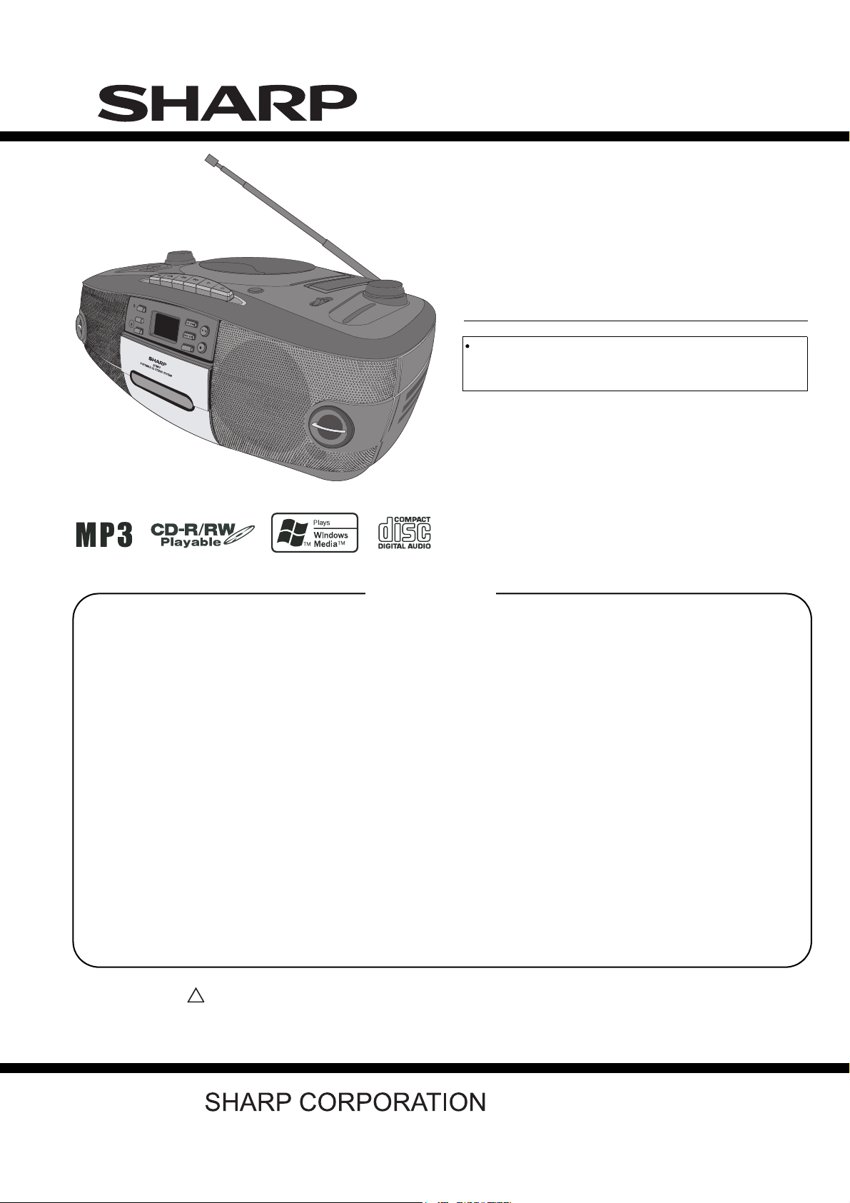
PORTABLE CD STEREO SYSTEM
/
CONTENTS
CHAPTER 1. GENERAL DESCRIPTION
[1] Precaution For Using Lead-Free Solder ....... 1-1
[2] Safety Precaution For Service Manual.......... 1-2
[3] Voltage Selection .......................................... 1-2
[4] AC Power Supply Cord and
AC Plug Adaptor ........................................... 1-2
[5] Specifications ................................................ 1-3
[6] Names Of Parts............................................. 1-4
CHAPTER 2. ADJUSTMENTS
[1] Tuner Section................................................ 2-1
[2] Mechanism Section....................................... 2-2
CHAPTER 3. BLOCK DIAGRAM
[1] Block Diagram............................................... 3-1
MODEL
In the Interests of user-safety the set should be restored to
its original condition and only parts identical to those
specified be used.
CHAPTER 5. CIRCUIT SCHEMATICS AND PARTS
LAYOUT
[1] Notes On Schematic Diagram .......................5-1
[2] Types Of Transistor And LED ........................5-1
[3] Schematic Diagram .......................................5-2
[4] Wiring Side Of PWB ....................................5-12
CHAPTER 6. FLOWCHART
[1] Troubleshooting.............................................6-1
CHAPTER 7. OTHERS
[1] Function Table Of IC......................................7-1
[2] LCD Display.................................................7-10
PARTS GUIDE
QT-MP3W
CHAPTER 4. CIRCUIT DESCRIPTION
[1] Waveforms Of CD Servo Circuit ....................4-1
[2] IC Voltage......................................................4-3
Parts marked with " " are important for maintaining the safety of the set. Be sure to replace these parts with specified ones
for maintaining the safety and performance of the set.
!
This document has been published to be used
for after sales service only.
The contents are subject to change without notice.
– 1
Page 2
QT-MP3W
CHAPTER 1.
AudioXL-MP150Service ManualXLMP150Market
[1] Precautions For Using Lead-Free Solder
GENERAL DESCRIPTION
1.Employing lead-free solder
"AUDIO, CONTROL, RECTIFIER, CD, TUNER, TAPE PWB" of this model employs lead-free solder.
The LF symbol indicates lead-free solder, and is attached on the PWB and service manuals. The alphabetical
character following LF shows the type of lead-free solder.
Example:
Indicates lead-free solder of tin, silver and copper.
2.Using lead-free wire solder
When fixing the PWB soldered with the lead-free solder, apply lead-free wire solder. Repairing with
conventional lead wire solder may cause damage or accident due to cracks.
As the melting point of lead-free solder (Sn-Ag-Cu) is higher than the lead wire solder by 40 C, were
commend you to use a dedicated soldring bit, if you are not familiar with how to obtain lead-free wire solder or
soldering bit, contact our service station or ser vice branch in your area.
3.Soldering
As the melting point of lead-free solder (Sn-Ag-Cu) is about 220 C which is higher than the conventional lead
solder by 40 C, and as it has poor solder wettability, you may be apt to keep the soldering bit in contact with the
PWB for extended period of time. However, since the land may be peeled off or the maximum heat-resistance
temperature of parts may be exceeded, remove the bit from the PWB as soon as you confirm the steady
soldering condition.
Lead-free solder contains more tin, and the end of the soldering bit may be easily corrected. Make sure to turn on
and off the power of the bit as required.
If a different type of solder stays on the tip of the soldering bit, it is alloyed with lead-free solder. Clean the bit
after every use of it.
When the tip of the soldering bit is blackened during use, file it with steel wool or fine sandpaper.
Be careful when replacing parts with polarity indication on the PWB silk.
Lead-free wire solder for servicing
Ref No.
PWB-A1
PWB-A2
PWB-A3
PWB-A4
PWB-B
PWB-C
Parts No.
92LMP300280047
92LMP300380092
92LMP301280047
92LMP300180024
92LMP300980056
92LMP301380047
AUDIO
CONTROL
RECTIFIER
TUNER
CD
TAPE
Description
1 – 1
Page 3
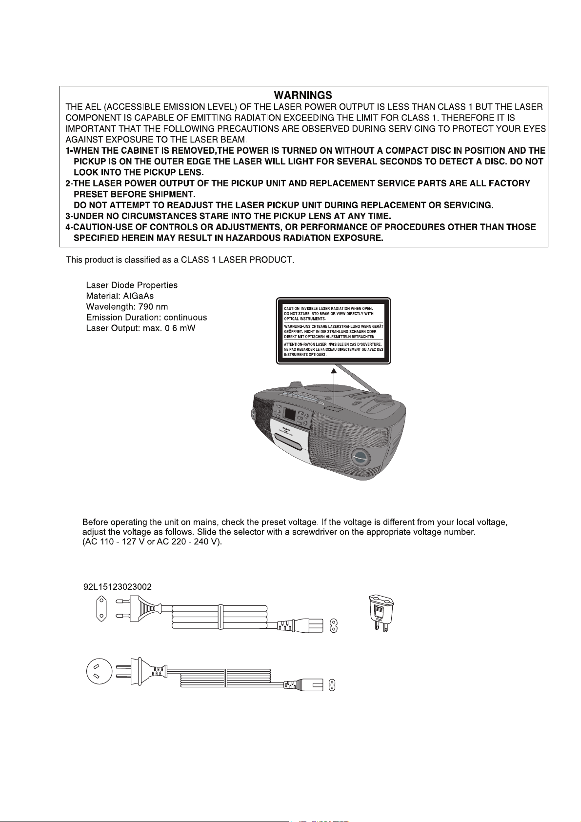
[2] Safety Precaution For Service Manual
Precaution to be taken when replacing and servicing the Laser Pickup.
QT-MP3W
[3] Voltage Selection
[4] AC Power Supply Cord and AC Plug Adaptor
92L15124023002
/
92L15911022019
1 – 2
Page 4
QT-MP3W
[5] Specifications
FOR A COMPLETE DESCRIPTION OF THE OPERATION OF THIS UNIT, PLEASE REFER
TO THE OPERATION MANUAL.
As part of our policy of continuous improvement, SHARP reserves the right to make design and
specifcation changes for product improvement without prior notice. The performance specification
figures indicated are nominal values of production units .There maybe some deviations from these
values in individual units.
Tape recorder
General
■
Power source
Power
consumption
Output power
Speakers
Dimensions
Weight
Radio
■
Frequency range FM: 88 - 108 MHz
AC 110 - 127/ 220 - 240 V, 50/60 Hz
DC12V ["D" size (UM/SUM-1, R20 or HP-
2) battery x 8]
Power on: 13 W
Power stand-by: 1.4 W
RMS : 4 W (2 W + 2 W)
(DC OPERATION, 10% T.H.D)
9 cm (3-1/2") full range speaker x 2
Width: 410 mm (16-1/8")
Height: 150 mm (6")
Depth: 245 mm (9-1/2")
2.7 kg (5.9 lbs.) without battery
AM: 531 - 1602 kHz
■
Frequency response 80 - 8,000 Hz (Normal tape)
Signal/noise ratio 40 dB
Wow and flutter 0.3% (WRMS)
Motor DC 9 V electric governor
Bias system AC bias
Erase system Magnet erase
CD player
■
Type Compact disc player
Signal readout Non-contact, 3-beam semiconductor
D/A converter 1-bit D/A converter
Frequency
response
laser pickup
60 - 20,000 Hz
1 – 3
Page 5
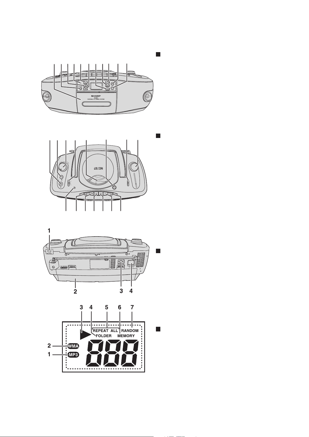
[6] Names Of Parts
r
21 3 4 5 6 7 8 9 10 11
QT-MP3W
Front panel
1. Cassette Compartment
2. FM Stereo Indicator
3. Folder Down Button
ON
/
4. Power on Indicator
5. Folder Up Button
6. Memory Button
7. Repeat/Random Button
8. Fast Reverse/Track Down Button
9. Fast Forward/ Track Up Button
10. Play/Pause Button
11. Stop Button
3
U
M
L
O
E
V
M
IN
MAX
X-BASS
OFFON
TAPE (STAND-BY)
CD
RADIO
FUNCTION
MIC
PAUSE
STOP/EJECT F.FWD REWIND PLAY RECORD
10 11 12 13 14 15
9
6542178
Top panel
1. Headphone Socket
2. X-Bass On/Off Button
3. Volume Control
N
I
G
N
U
T
KHz
Hz
M
1600
08
1
1400
1200
06
1
4
1000
0
1
2
10
800
00
1
00
7
AM
E
S
O
L
C
/
H
S
U
P
N
E
P
O
96
FM
0
60
2
9
0
9
530
8
8
AM
BAND
M
F
4. Function switch
5. CD Compartment
6. CD Door Open Button
7. Tuner Band Selector
8. Tuning Control
9. Build-in Mic
10. Tape Pause Button
11. Tape Stop/Eject Button
12. Tape Fast Forward Button
13. Tape Rewind Button
14. Tape Play Button
15. Tape Record Button
Back Panel
1. FM Stereo/Mono mode/Beat Cancel Selecto
2. Battery Compartment
3. Voltage Selector
4. AC Input Socket
Display
1. MP3 Indicator
2. WMA Indicator
3. Disc Play Indicator
4. Folder Indicator
5. Repeat mode Indicators
6. Memory Indicator
7. Random Indicator
1 – 4
Page 6
QT-MP3W
CHAPTER 2. ADJUSTMENTS
[1] Tuner Section
Use a plastic screw driver for adjustments.
Adjust the intermediate frequency of AM and FM to the frequency of ceramic filter.
Set of unit
Supply voltage
speaker impedance
standard output
Function switch
Parts Location:
DC 12.0V
:
4ohms
:
50 mW
:
RADIO
:
T103
L101
C2
C4
T101
a. AM Adjustment
2
3
4
5
Adjusting
Circuit
IF1
Tuning
coverage
Tracking
Step
b. FM Adjustment
Step
Adjusting
Circuit
C1
L102
C3
Band switch: MW
Connections
Input Output
Closed the output Connect sweep
termial by sweep generator to 465 KHz Low T103
generator, it place
to MW ANT
Connect AM SG to Connect VTVM to
test loop speaker terminals.
Connect AM SG to Connect VTVM to
test loop speaker terminals.
IC101(17) PIN(A)
SG Position of VTVM
Frequency Tuning dial Oscilloscope
522 KHz Low end T101
1620 KHz High end C4
600 KHz 600 KHz MW ANT COIL Max.
1400 KHz 1400 KHz C3 Max.
Adjustment
Band switch: FM FM Dummy antenna: 75 ohms unbalance
Connection
Input Output
SG Position of VTVM
Frequency Tuning dial Oscilloscope
Adjustment
2
3
4
5
Tuning
coverage
Tracking
Connect FM SG to Connect VTVM to
FM.ANT & D101(-) speaker terminals.
Connect FM SG to Connect VTVM to
FM.ANT & D101(-) speaker terminals.
87.35 MHz Low end L102
108.25 MHz High end C1
90.0 MHz 90.0 MHz L101 Max.
106.0 MHz 106.0 MHz C2 Max.
2 – 1
Page 7
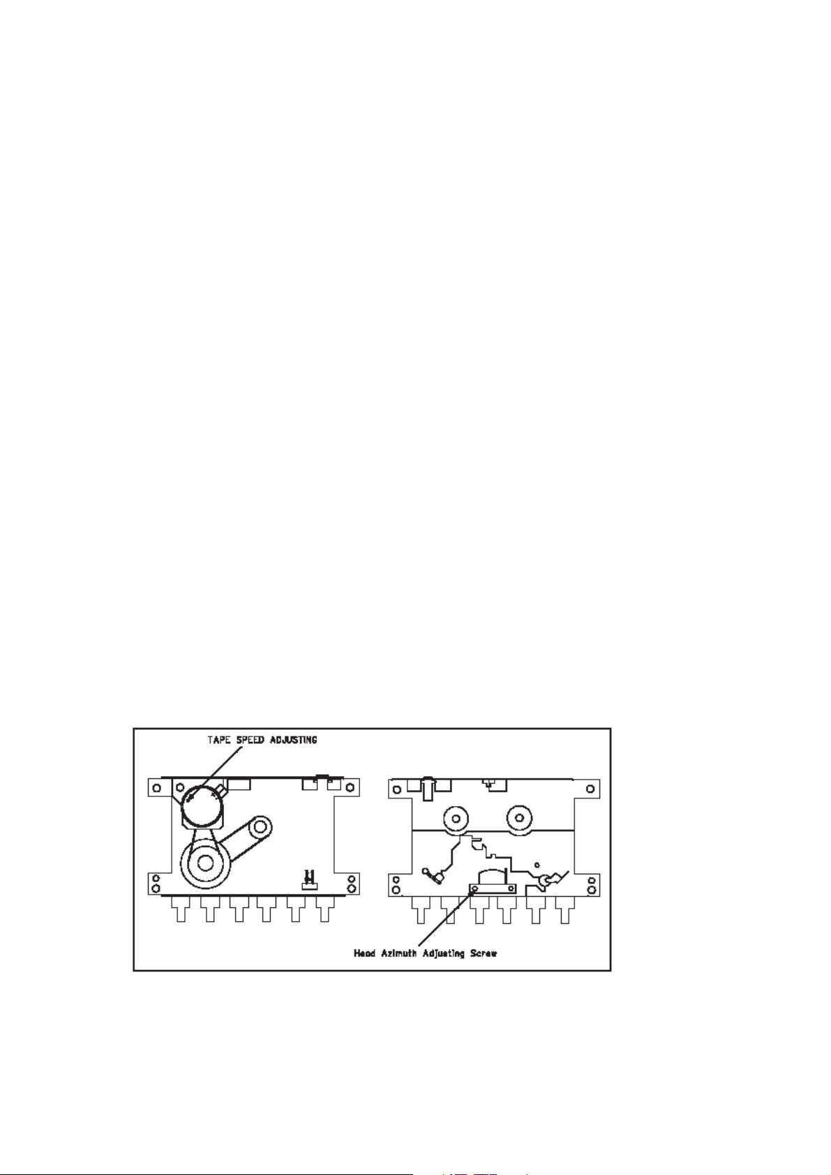
[2] Mechanism Section
1 HEAD AZIMUTH ADJUSTMET
( 1 )Load the test tape TCC-182A 8KHz for azimuth
adjustment.
( 2 )Press the PLAY button.
( 3 )Use a cross-tip screwdriver to turn the screw for azimuth
adjustment so that the left and right output are maximized.
( 4 )Press the STOP button.
( 5 )After completion of the adjustment. Use thread lock (TB-1401B)
to secure the azimuth-adjustment screw.
2 AC BIAS FREQUENCY ADJUSTMENTS
( 1 )Connect frequency counter to CN201 (BS).
( 2 )R/P swith in recording state.
( 3 )Adjusting T201 use a plastic screwdriver, AC bias frepuency; 62+-1KHZ.
QT-MP3W
3 TAPE SPEED ADJUSTMENT
( 1 )Insert the test tape (MTT-111N,3,000 HZ).
( 2 )Press the PLAY button.
( 3 )Use a flat-tip screwdriver to turn the MOTOR VR.
Adjust MOTOR VR so that the frequency counter
become 3,000Hz.
CASSETTE MECHANISM SECTION
CASS DECK
2 – 2
Page 8
QT-MP3W
Ө
HEAD AZIMUTH ADJUSTING SCREW
Tape recorder section
Items
Confirmation
of head angle
Confirmation Adjust VR401 so that the frequency counter
of tape speed
Reference Values for Confirmation Items
Measurement
conditions
:Test tape
TCC-182A (8KHz)
:Measurement output
terminal
Speaker terminal
Sparker R
(Load resistance:
8Ө
)
Headphone terminal
:Test tape
TCC-112 (3KHz)
:Measurement output
terminal
Headphone terminal
1 Playback the test tape TCC-182A (8KHz) Maximum Adjust the head
left and right output levers become
maximum, After adjustment, lock the head
azimuth at least by half turn.
playing back the test tape TCC-112 (3KHz)
with ending forward winding of the tape.
Measurement method
Standard
Values
output azimuth screw
Tape speed MOTOR VR
of deck
:3,010Hz
+/-15Hz
Adjusting
positions
only
Items
Wow & flutter When the test tape TCC-112 (3KHz) has
Measurement
conditions
:Test tape
TCC-112(3KHz)
:Measurement output
terminal
Headphone terminal
Measurement method
been mechanism at the beginning of
forward wow & flutter should be 0.25% or
less (WRMS).
Standard
Values
0.25% or
less
(WRMS)
Adjusting]
positions
2 – 3
Page 9
Electrical Performance
QT-MP3W
Items
Adjustment of
recording bias
current
(Reference
Value)
Adjustment of
recording and
playback
frequency
characteristics
Measurement
conditions
:Mode
Playback mode
Recording mode
:Test tape
TDK-D60
:Measurement
output terminal
Both recording and
headphone
terminals
:Reference frequency
1KHz and 8KHz
(REF.:- 10dB)
:Test tape
TDK-D60
:Measurement
input terminal
OSC IN
Standard Adjusting
Values
1 With the recording and playback
mechanism, load the test tapes
TDK-D60, and set the mechanism to the
recording and pausing condition in advance.
2 After connecting 100 in series to the
recorder head, measure the bias current
with a valve voltmeter at both of the
terminals.
1 With the recording and playback Output
mechanism, load the test tapes (TDK-D60) deviation
and set the mechanism to the
recording and pausing condition in
advance.
2 While repetitively inputting the reference
frequency signal of 1KHz and 8KHz from
OSC IN, record and playback the tape.
3 While receding and playback the test tape
Lch and Rch so that the output
deviation between 1KHz and 8KHz
becomes -1dB +/-2dB.
TDK-D60
4.5
A
+/-0.5 A
between
1KHz and
8KHz
:-1dB +/-2dB
positions
Reference Values for Electrical Function Confirmation Items
Items
Recording
bias
frequency
Measurement
conditions
Playback
:Test tape
TDK-D60
:Measurement
terminal
BIAS TP on
P.C. board
1 While changing over to and form BIAS 1
and 2, confirm that the frequency is
changed.
2 With the recording and playback
mechanism, load the test tape.
(TDK-D60), and set the mechanism to the
recording and pausing condition in advance.
3 Confirm that the BIAS TP frequency on the
P.C. board is 62KHz +/-6KHz.
Measurement method
Standard Adjusting
Values positions
62KHz T201
+/-6KHz
2 – 4
Page 10
QT-MP3W3
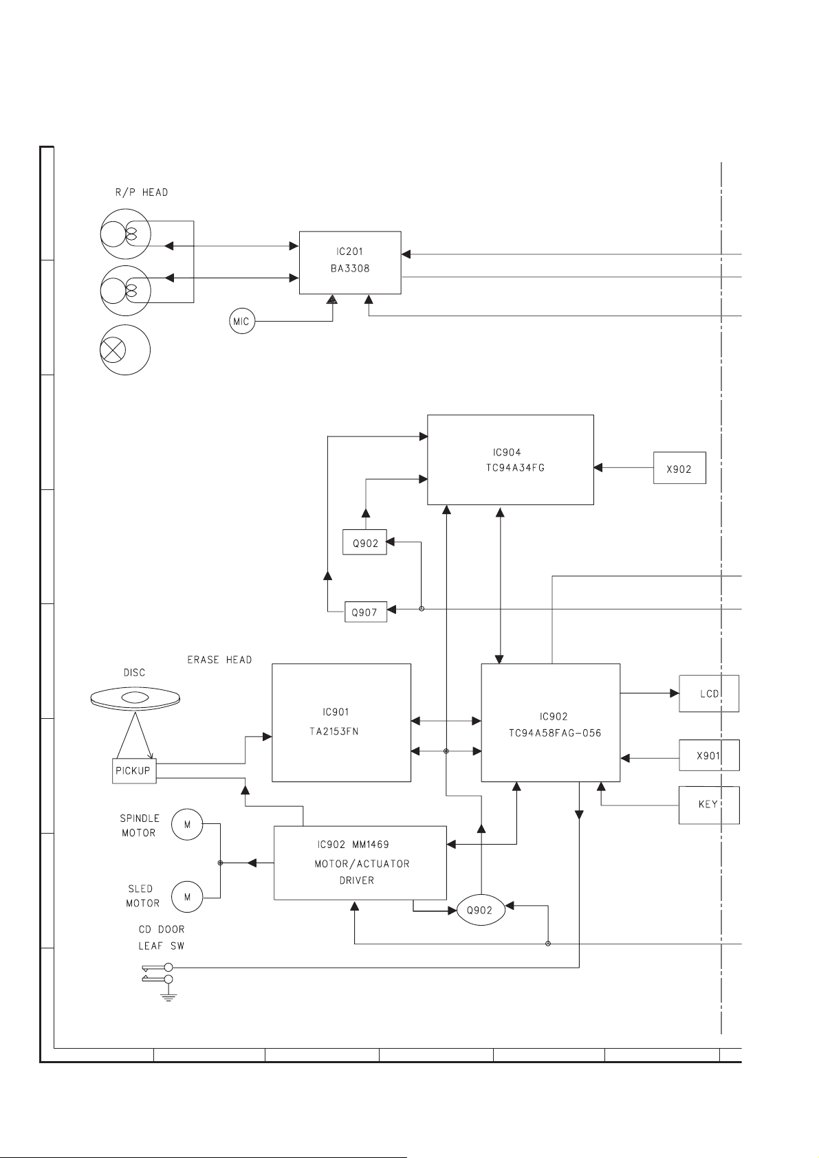
CHAPTER 3. BLOCK DIAGRAM
A
B
C
D
E
F
G
H
1
23456
Figure 1: BLOCK DIAGRAM (1/2)
3 – 1
Page 11
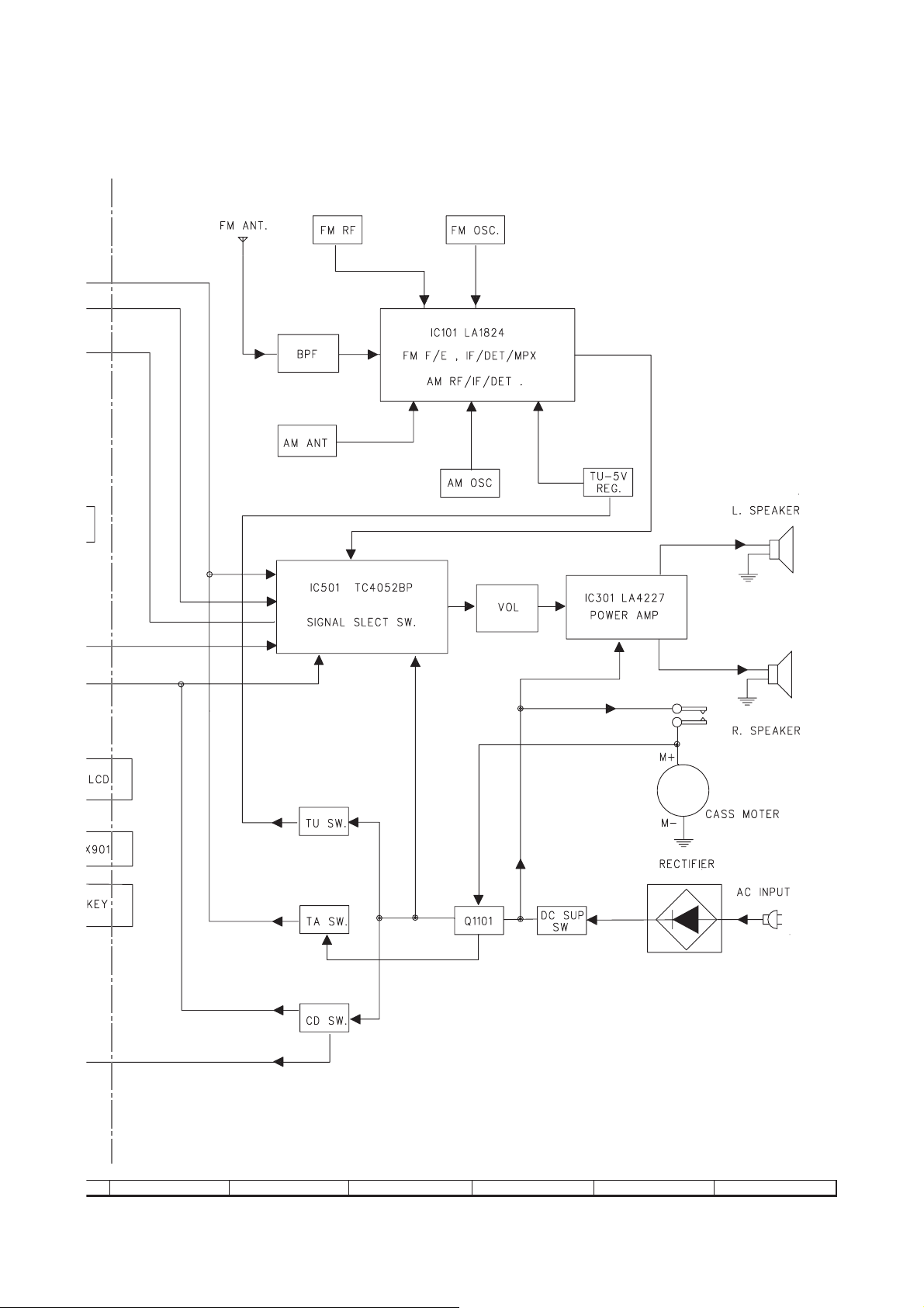
QT-MP3W
7
8 9 10 11 12
Figure 2: BLOCK DIAGRAM (2/2)
3 – 2
Page 12
QT-MP3W4
CHAPTER 4.
CIRCUIT DESCRIPTION
[1] Waveforms Of CD Servo Circuit
< Z1 : 2.5M > < Z1 :1 00K >
IC902 19
1
CH1 10:1
1.00 V/div
DC Full
< Z1 : 2M > < Z1 : 2M >
IC901 24
2
CH1 10:1
2.00 V/div
DC Full
CH 4
Display500ms/div
ONOFF
Position
-0.20div
Coupling
DC1M
Probe
10:1
Offset
0:32 V
Bandwidth
Full
Edge CH4
Auto
0.50 V
100ms/div 1s/div
Freq (C1)
50.00000kHz
Edge CH4
Auto
0.50 V
2
5
1
4
3
IC901 24
IC902 10
IC902 19
IC902 24
IC902 4
CH1 10:1
1.00 V/div
DC Full
CH1 10:1
2.00 V/div
DC Full
Freq(C1) *****
Freq(C1)
FR-A(C4)
CH2 10:1
2.00 V/div
DC Full
40.00000kHz
43.75492kHz
CH3 10:1
2.00 V/div
DC Full
Freq(C2) 50.00000kHz
CH4 10:1
2.00 V/div
DC Full
Edge CH4
Auto
0.50 V
Edge CH4
Auto
0.50 V
20µs/div
MEASURE
Mode
ON
Item Setup
Delay Setup
1Cycle Mode
OFF
Time Range1
1.57000div
Time Range2
1.77000div
CH 4
Display
ONOFF
Position
- 3.00div
Coupling
DC1M
Probe
10:1
Offset
0:82 V
Bandwidth
Full
ON
6
IC901 12
˜
0.2vCH1 A>0.2µs
9
8
7
IC901 21
IC901 22
IC901 23
CH1 10:1
5.00 V/div
DC Full
CH2 10:1
5.00 V/div
DC Full
< Z1 : 25K >
CH3 10:1
5.00 V/div
DC Full
Edge CH4
Auto
0.001 kV
4 – 1
Page 13

QT-MP3W
13
12
11
10
10
3
IC901 31
IC901 33
IC901 32
IC901 43
IC902 4
IC901 64
CH1 10:1
5.00 V/div
DC Full
CH2 10:1
2.00 V/div
DC Full
< Z1 : 2.5M >
CH3 10:1
2.00 V/div
DC Full
< Z1 : 2M >
CH4 10:1
2.00 V/div
DC Full
500ms/div
Edge CH4
Auto
0.50 V
1s/div
Freq (C1)
31.25000kHz
P1sN (C4)
1133
FR-A (C4)
5.891783kHz
Freq (C1)
22.22222kHz
CH1 10:1
2.00 V/div
DC Full
CH1 10:1
2.00 V/div
DC Full
Edge CH4
Auto
0.50 V
4 – 2
Page 14
QT-MP3W
[2] IC Voltage
IC904
TC94A34FG TC94A58FAG
PIN PIN PIN
VOLTAGE VOLTAGEVOLTAGE
NO NO NO NO
1 1.35 33 0.00 1 3.20 1 1.64 33 1.65 1 3.54
2 3.20 34 0.00 2 1.65 2 1.64 34 1.65 2 3.56
3 0.00 35 0.00 3 1.65 3 0.00 35 1.65 3 1.65
4 0.00 36 0.00 4 1.65 4 3.14 36 1.65 4 0.00
5 0.00 37 0.00 5 1.65 5 2.70 37 0.00 5 7.10
6 3.65 38 0.00 6 0.00 6 3.20 38 1.65 6 3.20
7 0.00 39 0.00 7 2.61 7 1.10 39 1.65 7 7.70
8 3.65 40 1.35 8 0.00 8 3.20 40 3.20 8 0.00
9 3.65 41 0.00 9 1.65 9 0.00 41 1.55 9 0.00
10 0.00 42 3.67 10 1.65 10 3.65 42 1.51 10 1.65
11 0.00 43 0.00 11 1.65 11 3.65 43 0.00 11 3.56
12 0.00 44 0.00 12 1.00 12 0.00 44 3.00 12 3.56
13 0.00 45 0.00 13 3.00 13 0.00 45 1.40 13 0.00
14 0.00 46 3.67 14 1.65 14 3.24 46 0.00 14 0.00
15 1.64 47 0.00 15 1.65 15 0.00 47 1.40 15 0.00
16 1.65 48 0.00 16 1.65 16 0.75 48 1.40 16 0.00
17 0.00 49 3.66 17 0.75 17 1.64 49 3.20 17 3.56
18 1.64 50 0.00 18 1.65 18 0.00 50 2.52 18 3.56
19 1.65 51 3.66 19 1.22 19 1.50 51 0.00 19 1.65
20 0.00 52 0.00 20 1.65 20 3.23 52 1.64 20 0.00
21 1.34 53 3.66 21 2.37 21 1.00 53 1.63 21 7.70
22 0.00 54 0.00 22 0.77 22 0.00 54 1.62 22 7.70
23 0.00 55 1.35 23 1.65 23 1.55 55 1.62 23 1.65
24 0.00 56 0.00 24 0.00 24 1.65 56 1.64 24 0.00
25 0.00 57 1.36 25 3.20 57 1.64 25 1.65
26 0.00 58 0.67 26 1.65 58 1.64 26 3.57
27 0.00 59 0.80 27 1.65 59 1.64 27 3.56
28 0.00 60 0.00 28 0.75 60 1.64 28 0.00
29 0.00 61 0.00
30 0.00 62 3.66 NO 30 1.00 62 1.65
31 0.00 63 0.00 1 0.00 31 1.65 63 1.64
32 0.00 64 0.95 2 0.00 32 1.65 64 3.20
PIN
IC901 IC902
TA2157FNG
VOLTAGE
IC501
TC4052BP
PIN
VOLTAGE
3 0.00
4 0.65 NO
5 0.00 1 13.20
6 0.00 2 6.50
7 0.00 3 12.20
8 0.00 4 1.17
9 0.00 5 0.00
10 3.64 6 13.10
11 0.40 7 0.00
12 0.00 8 0.00
13 0.00 9 1.17
14 0.00 10 12.20
15 0.00 11 6.50
16 5.36 12 13.80
1.65 61 1.64
PIN
NO
VOLTAGE
IC903
MM1669A
PIN
NO
IC301
LA4227
PIN
VOLTAGE
VOLTAGE
4 – 3
Page 15
QT-MP3W5
CHAPTER 5. CIRCUIT SCHEMATICS AND PARTS LAYOUT
[1] Notes On Schematic Diagram
•Resistor:
To differentiate the units of resistors, such symbol as
K and M are used: the symbol K means 1000 ohm
and the symbol M means 1000 kohm and the resistor without any symbol is ohm-type resistor.
Besides, the one with “Fusible” is a fuse type.
• Capacitor:
To indicate the unit of capacitor, a symbol P is used:
this symbol P means pico-farad and the unit of the
capacitor without such a symbol is microfarad. As to
electrolytic capacitor, the expression “capacitance/
withstand voltage” is used.
(CH), (TH), (RH), (UJ): Temperature compensation
(ML): Mylar type
(P.P.): Polypropylene type
• Schematic diagram and Wiring Side of P.W.Board
for this model are subject to change for
improvement without prior notice.
REF. NO DESCRIPTION POSITION
VR301 VOLUME MAX—MIN
SW701 USB ON—OFF
SW702 CD ON—OFF
SW703 Memo / Folder ON—OFF
SW704 Repeat / Random ON—OFF
SW705 Stop ON—OFF
SW706 Play/Pause ON—OFF
SW707 Fast Reverse / Track Down / Folder Down ON—OFF
SW708 Fast Forward / Track Up / Folder Up ON—OFF
• The indicated voltage in each section is the one
measured by Digital Multimeter between such a
section and the chassis with no signal given.
1. In the tuner section,
indicates AM
indicates FM stereo
2. In the audio section, a tape is being played back.
3. In the deck section, a tape is being played back.
( ) indicates the record state.
4. In the rectifier section, a tape is being played
back.
5. In the CD section, the CD is stopped.
• Parts marked with “ “ ( ) are
important for maintaining the safety of the set. Be
sure to replace these parts with specified ones for
maintaining the safety and performance of the set.
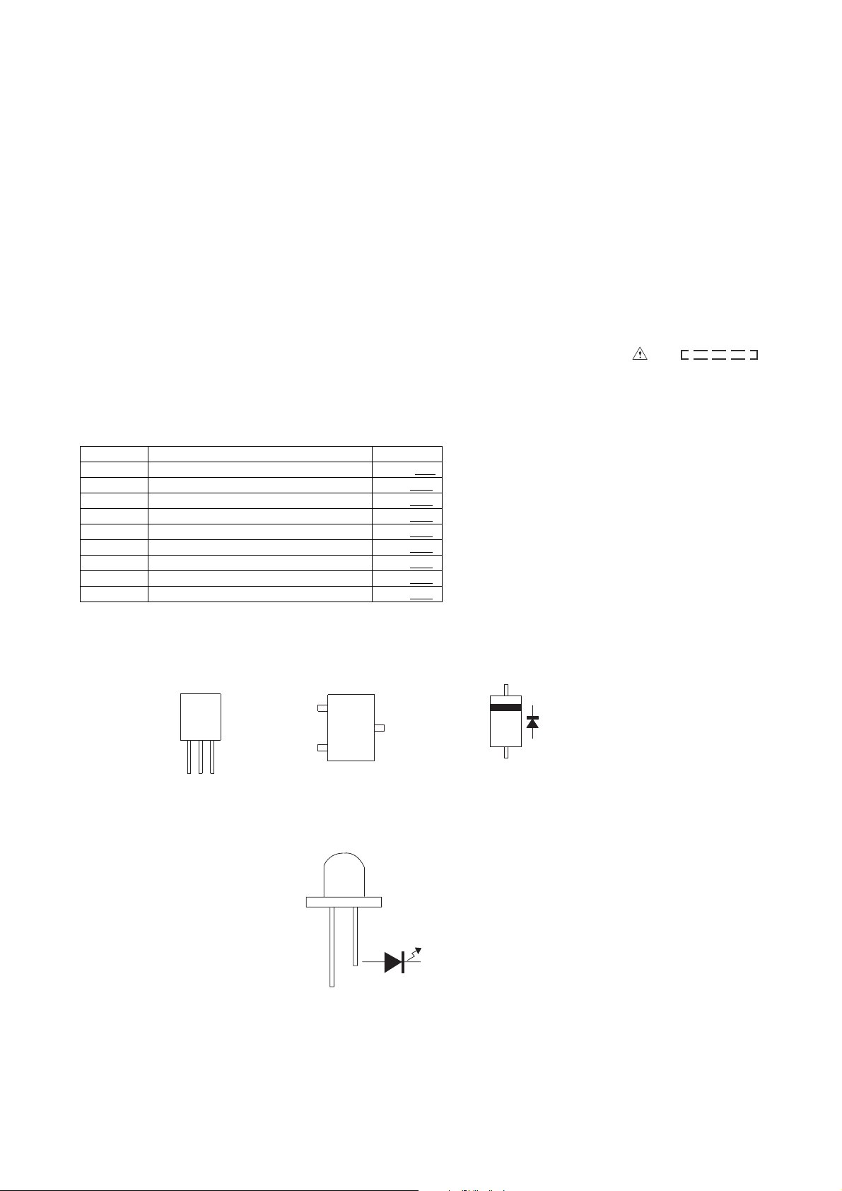
[2] Types Of Transistor And LED
FRONT
VIEW
ECB
(S)(G)(D)
(1)(2)(3)
B764
9014C
S8050
9015C
B
(3)
TOP
VIEW
E
(1)
HY3C
HY4C
92L22708030000
92L22708050012
92L22708050001
C
(2)
FRONT
VIEW
TOP VIEW
1N4001
1N4148
5 – 1
Page 16
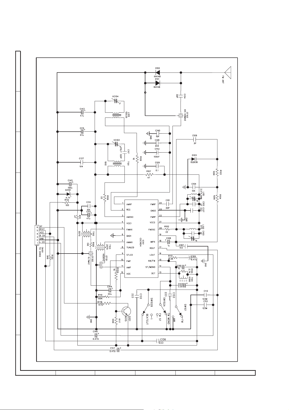
QT-MP3W
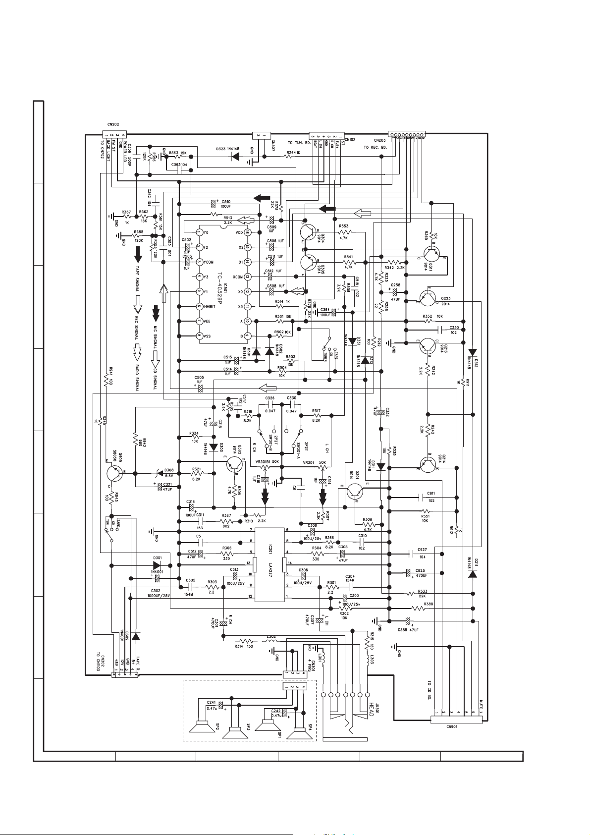
[3] Schematic Diagram
A
B
C
D
E
F
G
H
1
23456
Figure 5-1: TUNER SCHEMATIC DIAGRAM
5 – 2
Page 17
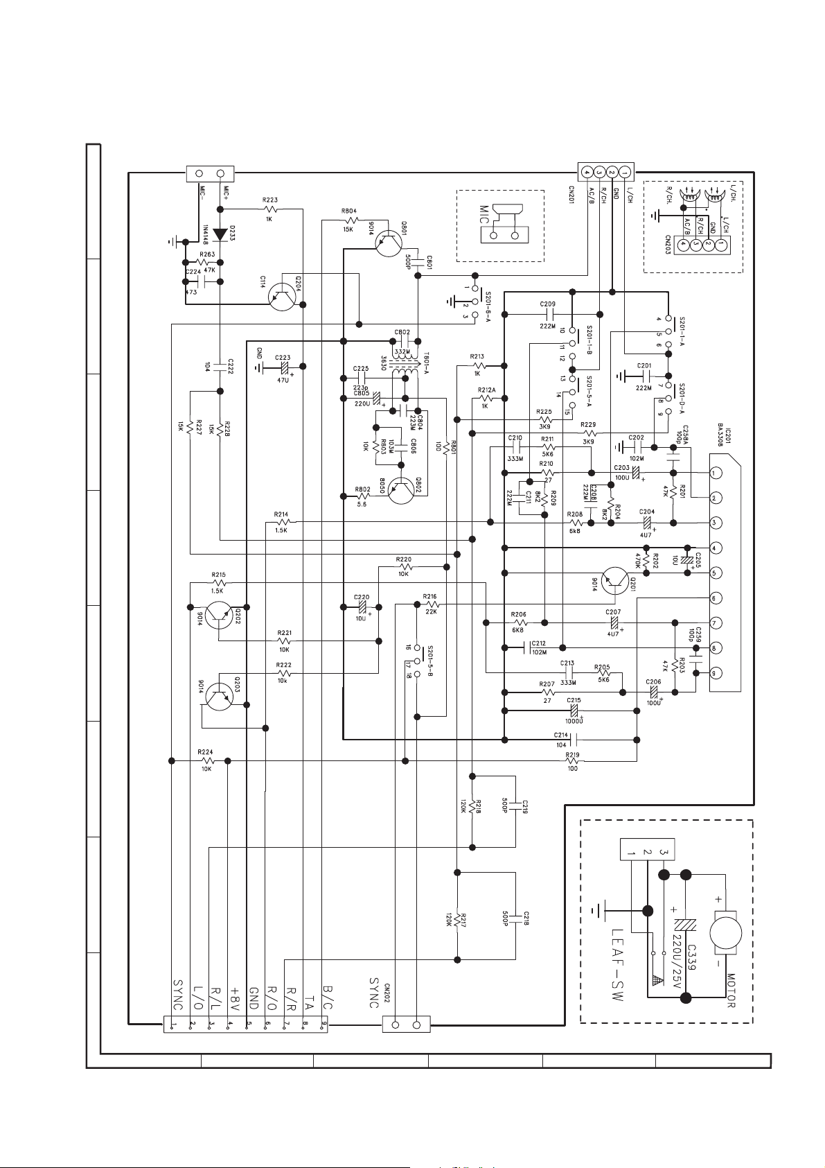
QT-MP3W
A
B
C
D
E
F
G
H
1
23456
Figure 5-2: DISPLAY SCHEMATIC DIAGRAM
5 – 3
Page 18
QT-MP3W
A
B
C
D
E
F
G
H
1
23456
Figure 5-3: AUDIO SCHEMATIC DIAGRAM
5 – 4
Page 19
QT-MP3W
A
B
C
D
E
F
G
H
1
23456
Figure 5-4: TAPE SCHEMATIC DIAGRAM
5 – 5
Page 20
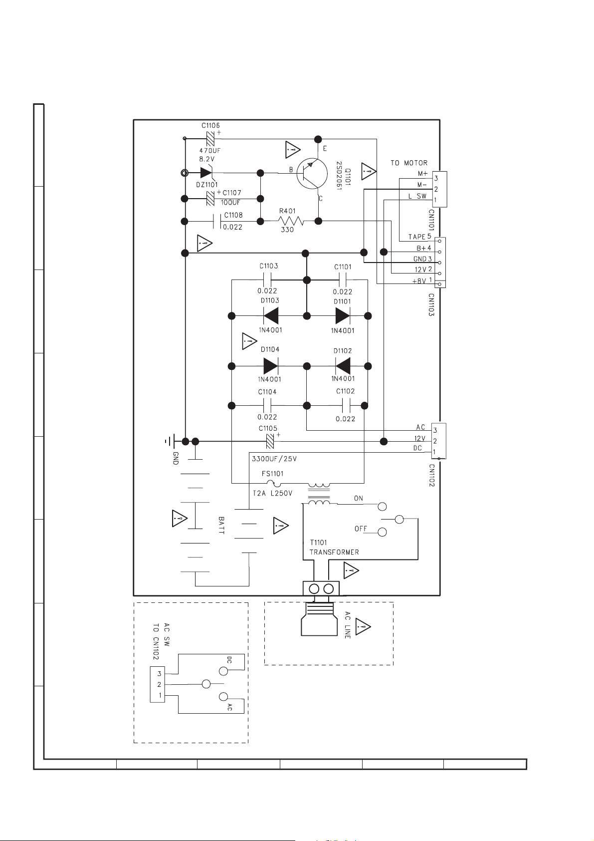
QT-MP3W
A
B
C
D
E
F
G
H
1
23456
Figure 5-5: POWER SCHEMATIC DIAGRAM
5 – 6
Page 21

-MEMO-
QT-MP3W
5 – 7
Page 22
QT-MP3W
A
B
C
D
E
F
G
H
1
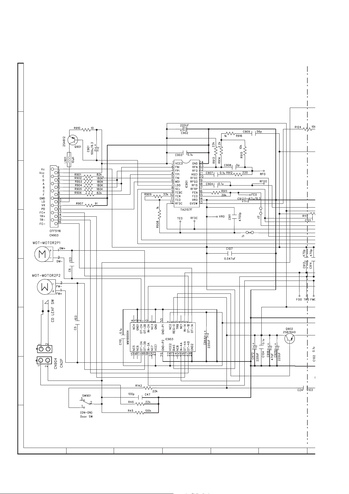
23456
Figure 5-6: CD SCHEMATIC DIAGRAM (1/4)
5 – 8
Page 23

QT-MP3W
7
8 9 10 11 12
Figure 5-7: CD SCHEMATIC DIAGRAM (2/4)
5 – 9
Page 24

QT-MP3W
A
B
C
D
E
F
G
H
1
23456
Figure 5-8: CD SCHEMATIC DIAGRAM (3/4)
5 – 10
Page 25

QT-MP3W
7
8 9 10 11 12
Figure 5-9: CD SCHEMATIC DIAGRAM (4/4)
5 – 11
Page 26
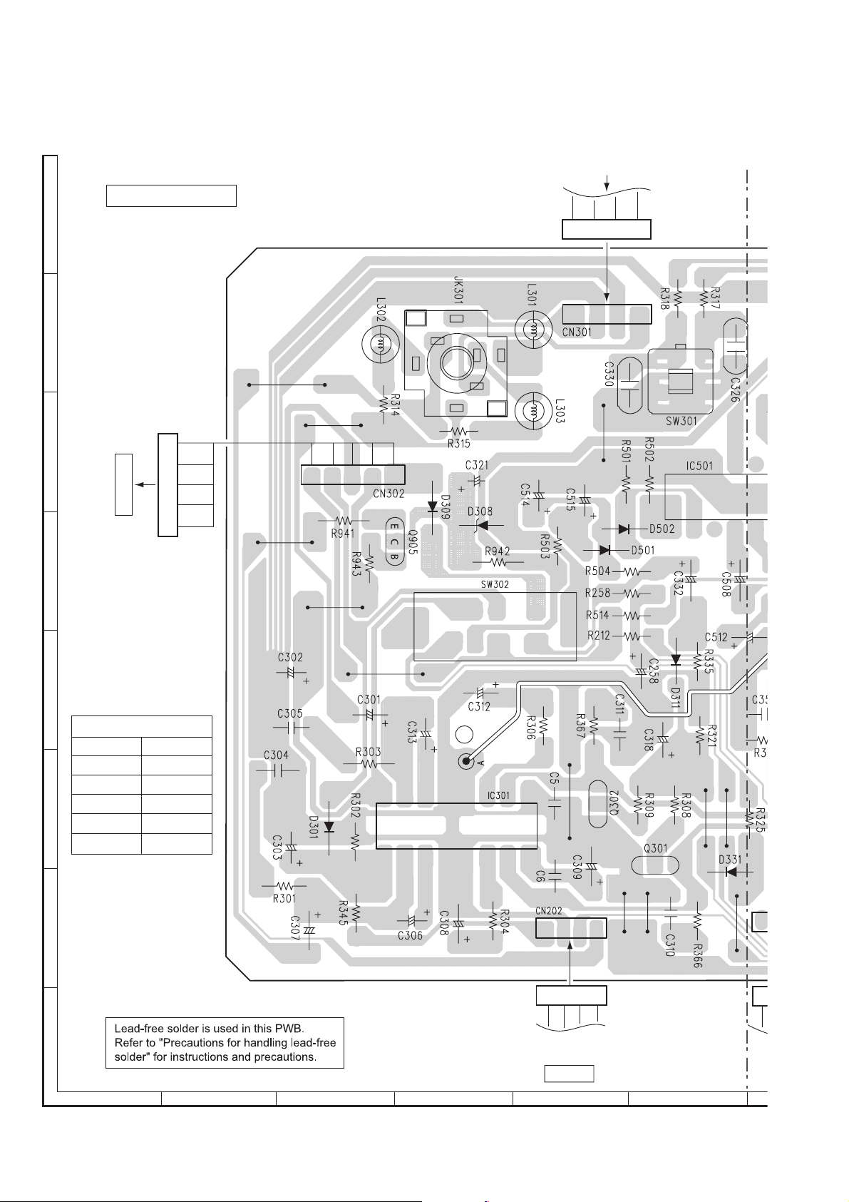
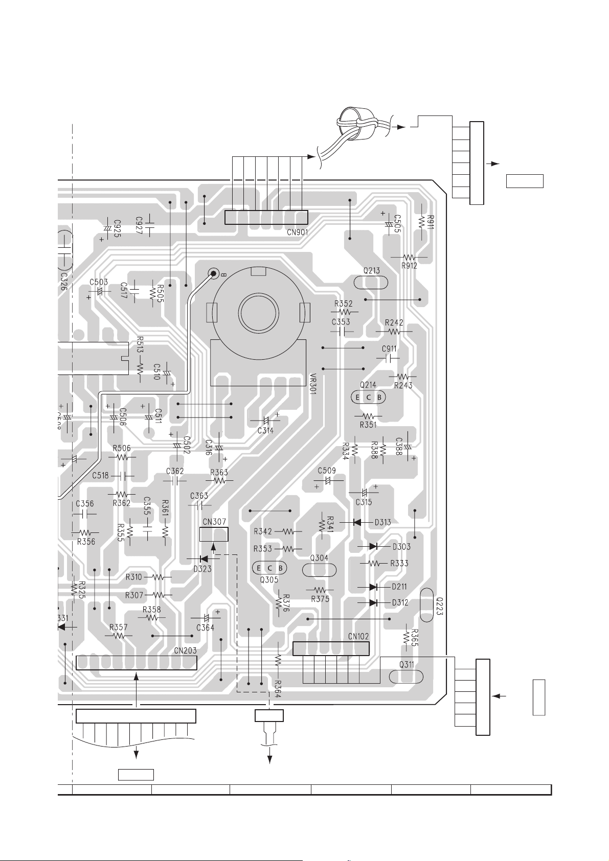
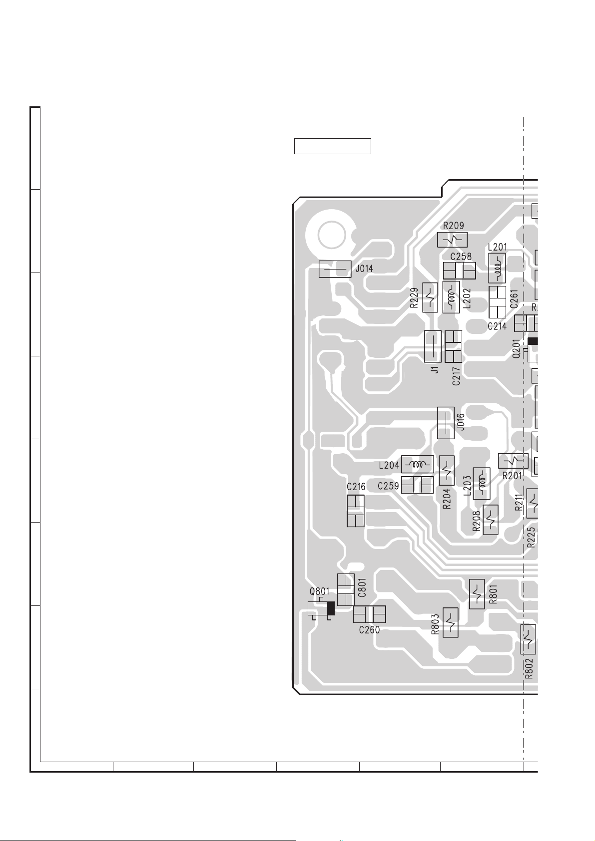
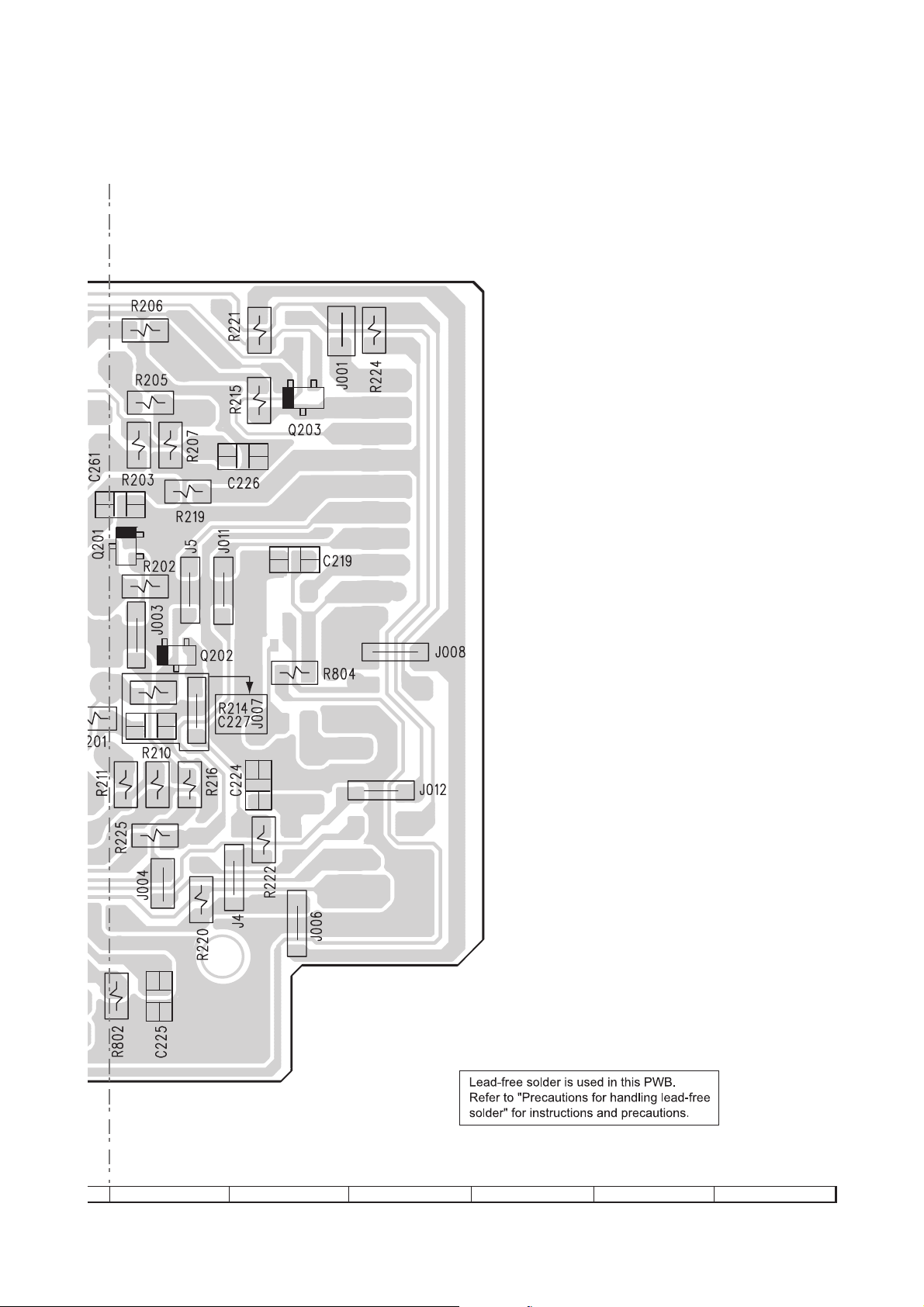
QT-MP3W55
[4] Wiring Side Of PWB
AUDIO PWB-A1
A
B
C
103
TO
CN1
RECTIFIER PWB-A3
2345
1
GY
GY
GY
GY
OR
GY
GY
GY
GY
OR
12345
FROM SPEAKER UNIT
BK
BR
BK
RD
1234
1234
D
E
COLOR TABLE
GY GRAY
OR ORANGE
RD RED
BR BROWN
F
BK BLACK
WH WHITE
G
CNS302
WIR 1
BCE
BCE
1234
1
1234
CNS702
GYGYGY
OR
H
FROM
CONTROL PWB-A2
1
OR
CN702
1
23456
Figure 5-10: WIRING SIDE OF AUDIO PWB (TOP VIEW) (1/2)
5 – 12
Page 27
WIR 1
GYGYGYGYGY
1234567
GY
OR
CORE
BCE
GY
GY
GY
GY
GY
GY
OR
QT-MP3W
TO
CD PWB-B
CN902
1234567
CNS901
12345678910
12345678910
GYGYGYGYGYGYGYGYGY
OR
TO TAPE PWB-C
CN202
7
8 9 10 11 12
21
BCE
654321
CNS203
21
BK WH
GYGYGYGYGY
CNS307
OR
BCE
TO MIC INPUT
Figure 5-11: WIRING SIDE OF AUDIO PWB (TOP VIEW) (2/2)
5 – 13
BCE
GY
GY
GY
GY
GY
GY
TO
654321
CNS102
CN101
TUNER PWB-A4
Page 28

QT-MP3W
A
B
C
CONTROL PWB-A2
321
OR
GY
GY
GY
1234
1234
TO
AUDIO PWB-A1
CN202
CNS702
COLOR TABLE
121110
D
987654321
OR ORANGE
GY GRAY
E
F
14 161210
1113 15
8642
161
161
CN901
FROM
CD PWB-B
G
13579
FFC703
H
1
23456
Figure 5-12: WIRING SIDE OF CONTROL PWB
5 – 14
Page 29

-MEMO-
QT-MP3W
5 – 15
Page 30
QT-MP3W
A
B
C
D
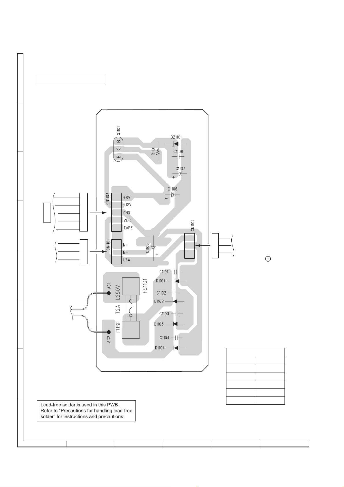
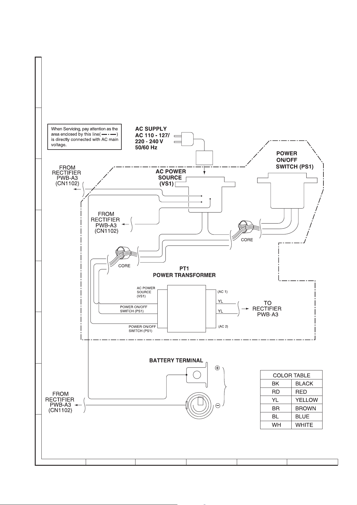
RECTIFIER PWB-A3
OR
GY
GY
FROM
AUDIO PWB-A1
FROM
CN302
GY
GY
WH
BK
RD
CNS302CNS1101
12345
123
12345
CNS1102
YL
AC POWER SOURCE (VS1)
123
1 2 3
WH
RD
1 2 3
BA TTER Y TERMINAL
FROM
&
( )
TAPE MOTOR
E
YL
(PT1)
FROM
F
YL
POWER TRANSFORMER
COLOR TABLE
BK BLACK
OR ORANGE
G
RD RED
WH WHITE
GY GRAY
YL YELLOW
H
1
23456
Figure 5-13: WIRING SIDE OF RECTIFIER PWB (1/2)
5 – 16
Page 31
QT-MP3W
A
B
C
RD
RD
YL
BK BL
BL BR RD
D
E
BK
BR
RD
F
RD
G
WH
DC
VOLTAGE
12 V
H
1
23456
Figure 5-14: WIRING SIDE OF RECTIFIER PWB (2/2)
5 – 17
Page 32

QT-MP3W
A
TUNER PWB-A4
A
TO
BAR ANTENNA
B
TO
BAR ANTENNA
RD
B
C
WH
D
E
F
G
H
1
23456
Figure 5-15: WIRING SIDE OF TUNER PWB (TOP VIEW) (1/2)
5 – 18
Page 33

QT-MP3W
TO
BAR ANTENNA
BK
TO
BAR ANTENNA
GR
2324 22 21 20 19 18 17 16 15 14 13
1234567891011
12
321
COLOR TABLE
GY GRAY
OR ORANGE
GR GREEN
BK BLACK
WH WHITE
RD RED
BCE
GYGYGY
GY
OR
FROM
AUDIO PWB-A1
CN102
124563
CNS102
124563
GY
7
8 9 10 11 12
Figure 5-16: WIRING SIDE OF TUNER PWB (TOP VIEW) (2/2)
5 – 19
Page 34

QT-MP3W
A
B
C
TUNER PWB-A4
D
E
F
G
H
1
23456
Figure 5-17: WIRING SIDE OF TUNER PWB (BOTTOM VIEW) (1/2)
5 – 20
Page 35

COLOR TABLE
WH WHITE
RD RED
BK BLACK
GR GREEN
WH RD BK GR
LUG 1
BAR ANTENNA
BR2
QT-MP3W
BR1
RA1
TO
TUNER PWB-A4
(Please see at top side
page 6-20 & 6-21)
ROD ANTENNA
7
8 9 10 11 12
Figure 5-18: WIRING SIDE OF TUNER PWB (BOTTOM VIEW) (2/2)
5 – 21
Page 36

QT-MP3W
A
B
C
D
CD PWB-B
EBC
EBC
COLOR TABLE
BR BROWN
E
RD RED
GY GRAY
OR ORANGE
FROM
CD DOOR
F
G
H
LEAF SWITCH
BR
RD
12
12
2468
1357 9
FROM
10 12 14 16
11 13 15
161
CONTROL PWB-A2
1
23456
Figure 5-19: WIRING SIDE OF CD PWB (TOP VIEW) (1/2)
5 – 22
Page 37

QT-MP3W
EBC
1
2
3
4
5
6
7
8
9
10
11
12
13
14
15
16
123456 7
1 2 3 4 5 6 CNS901
GY
GY
GY
GY
GY
GY
7
OR
FROM
CD PICK-UP
UNIT
FROM
AUDIO PWB-A1
CN901
7
8 9 10 11 12
Figure 5-20: WIRING SIDE OF CD PWB (TOP VIEW) (2/2)
5 – 23
Page 38

QT-MP3W
A
B
C
CD PWB-B
D
1
E
F
G
H
1
23456
Figure 5-21: WIRING SIDE OF CD PWB (BOTTOM VIEW) (1/2)
5 – 24
Page 39

QT-MP3W
IC902
IC904
7
89101112
Figure 5-22: WIRING SIDE OF CD PWB (BOTTOM VIEW) (2/2)
5 – 25
Page 40

QT-MP3W
A
B
C
TO
CN304
AUDIO PWB-A1
D
CNS304
GY
12345678910
GY
GY
GY
GY
GY
GY
GY
GY
OR
CNS202
12345678910
TAPE PWB-C
12345678910
CN202
E
F
G
EBC
Lead-free solder indication
Lead-free solder is used in the TAPE PWB.
Refer to "Precautions for handling lead-free solder" for
H
instructions
1
and precautions.
23456
Figure 5-23: WIRING SIDE OF TAPE PWB (TOP VIEW) (1/2)
5 – 26
Page 41

QT-MP3W
123456789
CNS201-A
1234
1234
YL
WH
BK
RD
TO
TAPE HEAD
COLOR TABLE
BK BLACK
WH WHITE
RD RED
EBC
7
8 9 10 11 12
Figure 5-24: WIRING SIDE OF TAPE PWB (TOP VIEW) (2/2)
OR ORANGE
YL YELLOW
GY GRAY
5 – 27
Page 42
QT-MP3W
A
B
C
D
TAPE PWB-C
E
F
G
H
1
23456
Figure 5-25: WIRING SIDE OF TAPE PWB (BOTTOM VIEW) (1/2)
5 – 28
Page 43
QT-MP3W
7
8 9 10 11 12
Figure 5-26: WIRING SIDE OF TAPE PWB (BOTTOM VIEW) (2/2)
5 – 29
Page 44

A
B
C
D
E
F
G
H
1
2 3 4 5 6
QT-MP3W
TAPE PWB-C
TO
CN203
12
34
RD
BK
WH
YL
RD
BL
TAPE PLAY
SWITCH
CNS203
TAPE MECHANISM
TAPE MOTOR
WH
1
BK
2
RD
WH
CAPACITOR
(220 µF/25 V)
BL
BK
3
CNS201
TO
TAPE PWB-C
CN201
COLOR TABLE
BK BLACK
WH WHITE
RD RED
YL YELLOW
BL BLUE
Figure 5-27: WIRING SIDE OF TAPE MECHANISM
5 – 30
Page 45
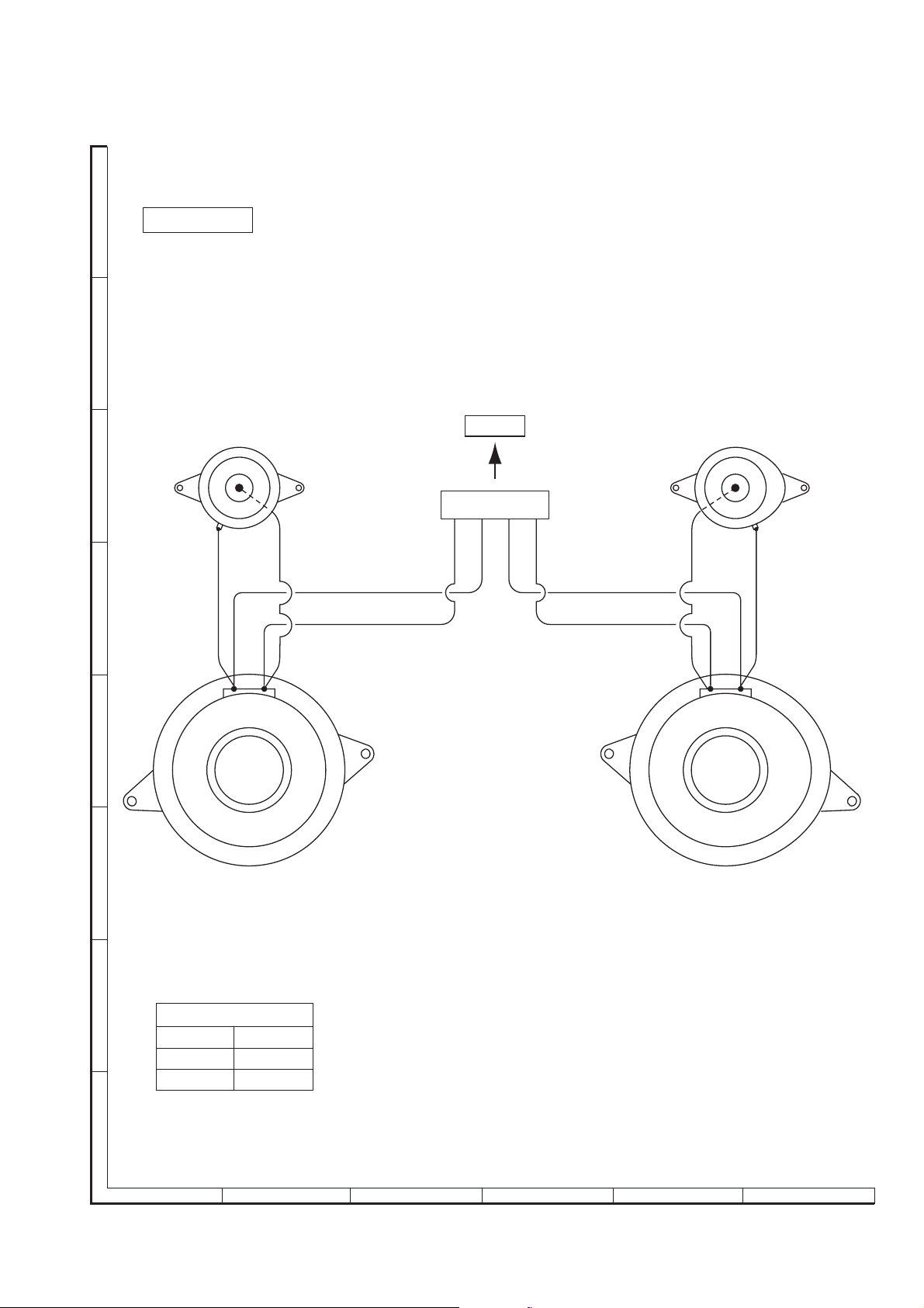
QT-MP3W
A
B
SPEAKER
R-CH
TO
L-CH
AUDIO PWB-A1
TWEETER
C
CN301
TWEETER
1234
BK RD
BK
D
BR
BR
BK
BK
RD
BK
BR
BKRD
BK BK
E
F
RD RD
WOOFERWOOFER
G
COLOR TABLE
BK BLACK
BR BROWN
RD RED
H
1
23456
Figure 5-28: WIRING SIDE OF SPEAKER
5 – 31
Page 46
QT-MP3W
CHAPTER 6. FLOWCHART
[1] Troubleshooting
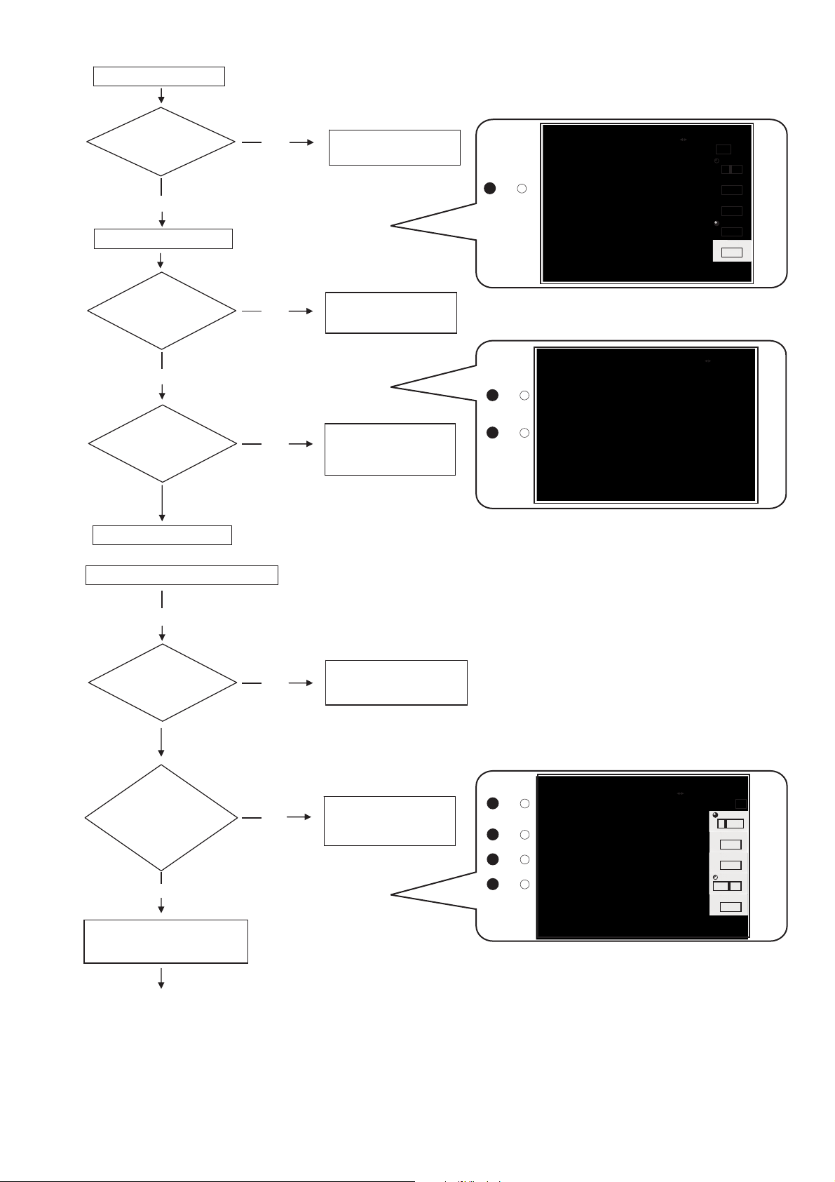
1. When the CD does not function
The CD section may not operate when the objective lens of the optical pickup is dirty. Clean the objective lens, and
check the playback operation. When this section does not opera te even af ter the abo ve step is t aken , check the fo llowing items.
Remove the cabinet and follow the trouble shooting instructions.
"Track skipping and/or no T OC (Table Of Conte nts) may be ca used by build up of du st other foreig n matter on the laser
pickup lens. Before attempting any adjustmen t make certain that the lens is clean. If not, clean it as mentioned below."
Turn the power off.
Gently clean the lens with a lens cleaning tissue and a small amount of isopropyl alcohol.
Do not touch the lens with the bare hand.
Parts code
1. CD optical pickup Lens cleaner disc UDSKA0004AFZZ
HOW TO USE
1.
Using the brush in the cleaner cap, apply 1 or 2 drops of the cleaning fluid to the
brush on the CD cleaner disc which has the mark next to it.
2.
Place the CD cleaner disc onto the CD disc tray with the brush side down, then
press the play button.
3.
You will hear music for about 20 seconds and the CD player will automatically stop.
If it still play continuously, press the stop button.
CAUTION
The CD lens cleaner should be effective for 30-50 operations, however if the
brushes become worn out earlier then please replace the cleaner disc.
If the CD cleaner brushes become very wet then wipe off any excess fluid with a soft
cloth.
Do not drink the cleaner fluid or allow it contact with the eyes. In the event of this
happening then drink and / or rinse with clean water and seek medical advice.
The CD cleaner disc must not be used on car CD players or on computer CD-ROM
drives.
All rights reserved. Unauthorized duplicating, broadcasting and renting this product
is prohibited by law.
2. When a CD cannot be played
Cleaning fluid
Cleaner disc
2.1. Pressing the CD operation key is accepted, but playback does not occur.
1) Focus-RF system check
2) Tracking system check
3) Spin system check
4) Others
6 – 1
Page 47
SC9641 reposit to 600MS
g
2
g
o
QT-MP3W
Confirm SLDGE
reposit or not?
YES
Start playback without Disc
Confirm Pick up
raise up down
focus aging
YES
Judge focus open
or close
?
Servohead inspect no disc
NO
NO
NO
Check SLED output and
drive circuit, see Figure 1
Checking FOC drive
information,see Fi
ure
Inspect the informationo of
LDON and the laser control
cricuit of SA9618
1
10
3
U902 19
U902 4
U901 64
CH1 10:1
1.00 V/div
DC Full
CH1 10:1
2.00 V/div
DC Full
CH1 10:1
2.00 V/div
DC Full
< Z1 : 2.5M >
< Z1 : 2M >
Edge CH4
Auto
0.50 V
Edge CH4
Auto
0.50 V
1s/div
CH 4
Display500ms/div
Position
-0.20div
Coupling
DC1M
Probe
10:1
Offset
0:32 V
Bandwidth
Full
Freq (C1)
22.22222kHz
ONOFF
Put disc and then re-start playback
YES
Whether disc is
stepped-up
playback
Whether the 56pin
information of SC9641
raise chan
e from high t
low
YES
Have lock track.under regular
condition, can find every drive
wave(figure-3)
NO
NO
Whether focus is regular or
not, inspect focus reposit
Track raise change and can
not block the original track,
inspect track
CH 4
1s/div
Display
Position
- 3.00div
Coupling
DC1M
Probe
10:1
Offset
0:82 V
Bandwidth
Full
ONOFF
CH3 10:1
2.00 V/div
DC Full
< Z1 : 2M >
Freq(C2) 50.00000kHz
Edge CH4
CH4 10:1
Auto
2.00 V/div
0.50 V
DC Full
U902 10
5
U902 19
1
U902 24
4
U902 4
3
Freq(C1)
40.00000kHz
FR-A(C4)
CH2 10:1
2.00 V/div
DC Full
43.75492kHz
CH1 10:1
2.00 V/div
DC Full
6 – 2
Page 48

QT-MP3W
g
Whether RF waveform is ok (ftgure4)
YES
Check whether
disc is good
YES
Confirm output
whether have noise
or wrong song
NO
Servo system ok
NO
YES
Check circuit of SA9618 of
RF
Confirm Disc
format whether
CDDA or not
YES
6
U901 12
NO
NO
˜
0.2vCH1 A>0.2µs
Whether 56pin
output raise any high
voltage impulse or
not
YES
C2 cannot rectify when raise
many wrong data under
Disc, as a result, which
readin
exist any wrong songs. Please
check Disc and whether Pickup is aging or not.
Confirm pin no. 24 output
is square wave of 88.2K is
stabil or not
YES
C2 cannot rectify if many
many wrong data during
read the Disc, cause wrong
song selected. Please
check Disc and whether
Pick-up is aging or not.
Confirm pin no.24 output
shows high voltage
impulse or not.
YES
6 – 3
Page 49

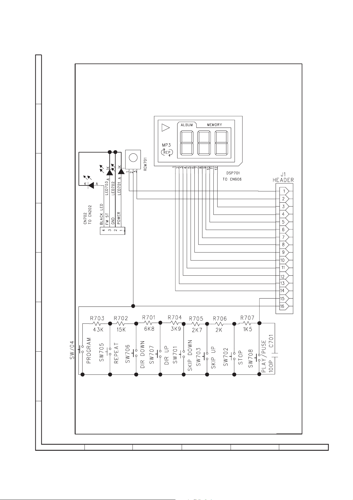
CHAPTER 7. OTHERS
[1] Function Table Of IC
U712 92L31012161601 : SDRAM (M12L161A)
QT-MP3W
V
DQ0
DQ1
VSS0
DQ2
DQ3
VDD0
DQ4
DQ5
VSS0
DQ6
DQ7
VDD0
LDQM
WE
CAS
RAS
A10/AP
VDD
DD
1
2
3
4
5
6
7
8
9
10
11
12
13
14
15
16
17
CS
18
BA
19
20
A0
21
A1
22
A2
23
A3
24
25
VSS
50
49
DQ15
48
DQ14
VSS0
47
46
DQ13
DQ12
45
44
VDD0
DQ11
43
42
DQ10
VSS0
41
DQ9
40
DQ8
39
VDD0
38
N.C/RPU
37
UDQM
36
CLK
35
CKE
34
N.C
33
A9
32
A8
31
A7
30
A6
29
A5
28
A4
27
VSS
26
I/O Control
CLK
ADD
Address Register
LCKE
LRAS
CLK
Bank Select
Refresh Counter
Row Buffer
Row Decoder
Data Input Register
Sense AMP
512 x 16
512 x 16
LCBR
LRAS
Col. Buffer
Column Decoder
Latency & Burst Length
Programming Register
LCBR LWE
CKE L(U)DQM
CS
LCAS
LWCBR
WERAS CAS
LWE
LDQM
Output Buffer
DQi
LDQM
Figure 7-1 BLOCK DIAGRAM OF IC
7 – 1
Page 50

QT-MP3W77
U710 92L31000250110 : CPU ( TS2501 ) ( 1/4 )
GPIO_D21
GPIO_D20
GPIO_D19
GPIO_D18
GPIO_D17
GPIO_D16
GPIO_D15
PKG1
VSSI_ADC
VDDI_ADC
VBBA_ADC
VSSA_ADC
ADIN4
ADIN2
ADIN0
VDDA_ADC
VBBA_PLL
VSSA_PLL
XFILT
VDDA_PLL
VDDIO
XOUT
XIN
READY
nRESET
VDD_OSC
XTOUT
XTIN
DAI/GPIO_B25
DAO/GPIO_B24
MCLK/GPIO_B23
VSSIO
VSSIO
MODE1
TDI
TMS
TCK
TDO
nTRST
SDO0/GPIO_A0
SCK0/GPIO_A1
SFRM0/GPIO_A2
SDI0/GPIO_A3
SDO1/GPIO_A4
VDDI
VSSI
SCK1/GPIO_A5
VDDIO
SFRM1/GPIO_A5
SDI1/GPIO_A7
SDO2/GPIO_A8
SCK2/GPIO_A9
SFRM2/GPIO_A10
SD12/GPIO_A11
VDDI
VSSI
EXINT0/GPIO_A12
EXINT1/GPIO_A13
EXINT2/GPIO_A14
EXINT3/GPIO_A15
XDD
XD1
XD2
XD3
96959493929190898887868584838281807978777675747372177069686766
97
98
99
100
101
102
103
104
105
106
107
108
109
110
111
112
113
114
115
116
117
118
119
120
121
122
123
124
124
126
127
128
12345678910111213141516171819202122232425262728293031
Ts2501
65
VDD-USB
64
LRCK/GPIO_B22
63
BCLK/GPIO_B21
62
UT_RX/IDE_nCS/GPIO_59
61
UT_TX/GPIO_88
60
nOE
59
nWE
58
ND_nWE/GPIO_B7
57
SD_CKE/GPIO_B0
56
VSSI
55
USBH_CN/GPIO_B29
54
USBH_DP/GPIO_B28
53
USB_DN/GPIO_B27
52
USB_DP/GPIO_B26
51
nCS3/nOE3/GPIO_B5
50
nCS/nOE2/GPIO_B4
49
nCS1/nOE1/GPIO_B3
48
nCS0/nOE0/GPIO_B2
47
SD_nCS/GPIO_B1
46
VSSIO
45
SD_CLK/GPO
44
XA21/DQM0
43
XA20/DQM1
42
VDD1
41
XA19
40
XA18
39
XA17/CLE
38
XA16/nRAS/ALE
37
XA15/nCAS
36
XA14/BA1
35
XA13/BA0
34
VDDIO
33
32
XD4
VSSIO
XD5
XD6
XD7
XA0
XD8
VSSI
VDDI
XD9
XD11
XD10
XD12
XD13
XD14
XD15
VDDIO
XA1
Figure 7-2 BLOCK DIAGRAM OF IC
7 – 2
XA2
XA3
XA4
XA5
XA6
VDDI
VSS1
XA7
XA8
XA9
1
XA1
XA10
XA12
VSSIO
Page 51

U710 92L31000250110 : CPU ( TS2501 ) ( 2/4 )
USB_DP/GPIO_B[28], USB_DN/GPIO_B[27]
USBH_DP/GPIO_B[28], USBH_DN/GPIO_B[29]
QT-MP3W77
DQM[0:1] / XA[21:20]
DQS[1:0] / XA[19:18]
ND_CLE / XA[17]
D_ALE / SD_nRAS / XA[16]
SD_nCAS / XA[15]
SD_BA[1:0] / XA[14:13]
XA[12:0]
XD[15:0]
nOE. nWE. nCS[3:0]
SD_nCS, SD_CKE
SD_CLK
ND_nWE
IDE_nCS1
READY
TDI. TMS. TCK
nTRST , TDO
GPIO_D[21:15]
GPIO_A[3:0]
Boot ROM
(4KB)
SRAM
(64KB)
Ext. Memory
Interface
AHB Wrapper
ARM940T
JTAG
Video Input
Interface
USB1.1
Host/Device
ECC
Generation
APB
Bridge
AHB Arbiter
DMA
(2-channel)
DAI (12S)
for
CODEC
&
CD-DSP
Pll &
CLK Generator
Timers/
Counters
Interrupt
Controller
GSIO
GPIO
UART/IrDA
12C
ADC
XIN, XOUT
XTIN, XTOUT
XFILT
TCO2/GPIO_A[11]
TCO5/GPIO_A[8]
TCO1/GPIO_A[7]
TCO4/GPIO_A[4]
TCO0/GPIO_A[3]
TCO3/GPIO_A[0]
EXINT[3:0] /
GPIO_A[15:12]
GPIO_A[11:0]
GPIO_A[15:0]
GPIO_B[20:21]
GPIO_B[9:7]
GPIO_B[5:0]
GPIO_D[17:15]
UT TX/GPIO_B[8]
UT RX/GPIO_B[8]
GPIO_A[11:10]
GPIO_A[9:8]
GPIO_D[17:16]
ADIN0
ADIN1
ADIN4
DAO / GPIO_B[24]
MCLK / GPIO_B[23]
BCLK / GPIO_B[21]
LRCKO / GPIO_B[22]
DAI / GPIO_B[25]
GPIO_A[3] / CDAI
GPIO_A[2] / CLRCK
GPIO_A[1] / CBCLK
Figure 7-3 BLOCK DIAGRAM OF IC
7 – 3
Page 52

QT-MP3W
U710 92L31000250110 : CPU ( TS2501 ) ( 3/4 )
PIN DESCRIPTION
Signal Name Shared Signal Pin # Type Description-TS2501
External Memory Interface Pins
SD_CKE GPIO_B[0] 56 I/O SDRAM Clock Enable signal. Active high. / GPIO_B[0]
SD_CLK GPO 44 I/O SDRAM Clock / GPO. SD_CLK can be used as a general purpose output.
SD_nCS SD_nCLK/
GPIO_B[1]
XA[21:20] DQM[0:1] 43:42 I/O External Bus Address Bit [21:20] / Data I/O Mask 0, 1
XA[19:18] DQS[1:0] 40:39 I/O External Bus Address Bit [19:18] / DDR SDRAM / GPIO_B[1]
XA[17] ND_CLE 38 I/O External Bus Address Bit [17] / CLE for NAND Flash
XA[16] SD_nRAS 37 I/O External Bus Address Bit [16] / SDRAM RAS signal / ALE for NAND Flash
XA[15] SD_nCAS 36 I/O External Bus Address Bit [15] / SDRAM CAS signal
XA[14] SD_BA[1] 35 I/O External Bus Address Bit [14] / SDRAM Bank Address 1
XA[13] SD_BA[0] 34 I/O External Bus Address Bit [13] / SDRAM Bank Address 0
XA[12:7] 31:26 I/O External Bus Address Bit [12:0]
XA[6:0] 23:17
XA[15:9] 15:9 I/O External Bus Address Bit [15:0]
XA[8:4] 6:2
XA[3:0] 128:125
NCS[3:0] ND_nOE[3:0] /
GPIO_B[5:2]
ND_nWE GPIO_B[7] 57 I/O NAND Flash WE. Active low. / GPIO_B[7]
nWE 58 I/O Static Memory Write Enable signal. Active low.
nOE 59 I/O Static Memory Write Output Enable signal. Active low.
READY 73 I Ready information from external device.
GPIO_B[0] SD_CKE 56 I/O GPIO[0] / SDRAM clock control
GPIO_D[21:18]FGPIO[14:11] /
CISD[7:4]
GPIO_D[17] FGPIO[10] / SCL
/ CISHS
GPIO_D[16] FGPIO[9] / SDA /
CISVS
GPIO_D[15] FGPIO[9] /
CISCLK
ADIN_0 - 82 AI General purpose multi-channel ADC input 0
ADIN_2 - 83 AI General purpose multi-channel ADC input 2
ADIN_4 - 84 AI General purpose multi-channel ADC input 4
XIN - 74 I Main Crystal Oscillator Input for PLL. 12MHz Crystal must be used if USB
XOUT - 75 O Main Crystal Oscillator Output for PLL
XFILT - 78 AO PLL filter output
XTIN - 69 I Sub Crystal Oscillator Input. 32.768kHz is recommended. Input voltage must
XTOUT - 70 O Sub Crystal Oscillator Output
MODE1 - 98 I Mode Setting Input 1. Pull-down for normal operation.
PKG1 - 89 I Package ID1. Pull-up for normal operation.
nRESET - 72 I System Reset. Active low.
TDI - 99 I JTAG serial data input for ARM940T
TMS - 100 I JTAG test mode select for ARM940T
TCK - 101 I JTAG test clock for ARM940T
TDO - 102 I/O JTAG serial data output for ARM940T. External pull-up resistor is required to
nTRST - 103 I JTAG reset signal for ARM940T. Active low.
VDDIO - 112
VDD_USB - 64 PWR Power for USB I/O (3.3V)
46 I/O Chip select signal for SDRAM, Active low / Inverted SD_CLK for DDR SDRAM
50:47 I/O External Bus Chip Select [3:0] / NAND Flash Output Enable [3:0] /
96:93 I/O GPIO_D[21:18] / Fast GPIO bits 14 ~ 11 / Camera Interface Data Inputs
92 I/O GPIO_D[17] / Fast GPIO bit 10 / 12C SCL / Camera Interface Hsync.
91 I/O GPIO_D[16] / Fast GPIO bit 9 / 12C SDA / Camera Interface Vsync.
90 I/O GPIO_D[15] / Fast GPIO bit 8 / Camera Interface Clock
PWR Digital Power for I/O (1.8V ~ 3.3V)
76
33
16
Refer to section “MEMORY CONTROLLER”.
(MCFG register Bit[3] and Bit [1])
/ GPIO_B[1]
GPIO_B[5:2]
SDRAM / Inverted Clock for DDR SDRAM.
3 ~ 0. Internal pull-up resistors are enabled at reset. GPIO_D[19:18] are
disabled in TS250IT(N.C).
ADC Input Pins
Clock Pins
Boot Mode is required. Input voltage must not exceed VDD_OSC
(1.95V max).
not exceed VDD_OSC (1.95V max).
Mode Control Pins
JTAG Interface Pins
prevent floating during normal operation.
Power Pins
7 – 4
Page 53

U710 92L31000250110 : CPU ( TS2501 ) ( 4/4 )
Signal Name Shared Signal Pin # Type Description-TS2501
VDD_OSC - 71 PWR Digital Power for Oscillators (1.8V)
VDDI - 119
109
41
24
7
VDDI_ADC - 87 PWR Digital Power for ADC (1.8V)
VDDA_ADC - 81 PWR Analog Power for ADC (3.3V)
VDDA_PLL - 77 PWR Analog & Digital Power for PLL (1.8V)
VSSIO - 97
65
45
32
1
VSSI - 120
110
55
25
8
VSSI_ADC - 88 GND Digital Ground for ADC
VBBA_ADC - 86 GND Analog Ground for ADC
VSSA_ADC - 85 GND Analog Ground for ADC
VBBA_PLL - 80 GND Analog Ground for PLL
VSSA_PLL - 79 GND Analog Ground for PLL
PWR Digital Power for Internal Core (1.8V)
GND Digital Ground for I/O
GND Digital Ground for Internal
QT-MP3W
7 – 5
Page 54

QT-MP3W77
U711 92L31003980031 : FLASH MEMORY ( SST39VF800A )
A15
A14
A13
A12
A11
A10
WE#
A18
A17
NC
NC
NC
NC
NC
NC
1
2
3
4
5
A9
A8
A7
A6
A5
A4
A3
A2
A1
6
7
8
9
10
11
12
13
14
15
16
17
18
19
20
21
22
23
24
SST39LF / VF800A
X-Decoder
48
47
46
45
44
43
42
41
40
39
38
37
36
35
34
33
32
31
30
29
28
27
26
25
SuperFlash
Memory
A16
NC
V
SS
DQ15
DQ7
DQ14
DQ6
DQ13
DQ5
DQ12
DQ4
V
DD
DQ11
DQ3
DQ10
DQ2
DQ9
DQ1
DQ8
DQ0
0E#
V
SS
CE#
A0
Memory Address
Address Buffer & Latches
Y-Decoder
CE#
OE#
Control Logic
I/O Buffers and Data Latches
WE#
DQ
Figure 7-4 BLOCK DIAGRAM OF IC
PIN DESCRIPTION
Symbol Pin Name Functions
1
-
A Address Inputs To provide memory addresses. During Sector-Erase address lines will select theA
MSDD0
DQ Data Input/output To ouput data during Read cycles and receive input data during Write cycles.
DQ
-
15 0
sector. During Block-Erase address lines will select the block.
Data is internally latched during a Write cycle.
-
AA
MS 15
The outputs are in tri-state when OE# or CE# is high.
CE# Chip Enable To activate the device when CE# is low.
OE# Output Enable To gate the data output buffers.
WE# Write Enable To control the Write operations.
V Power Supply To provide power supply voltage:
3.0-3.6V for SST39LF200A/400A/800A
2.7-3.6V for SST39VF200A/400A/800A
V Ground
SS
NC No Connection Unconnected pins.
1.
A Most significant address=
MS
A for SST39LF/VF200A,=MSA
16
for SST39LF/VF400A, andA
17
for SST39LF/VF800AA
18
-
AA
MS 11
-
15DQO
7 – 6
Page 55

U901 92L31000964110 : CD SERVO ( SC9641 )
R
VREF
VDD0
VSS0
VDDA
RESET
D
C
A
RAD
FOC
SLED
VSSP
BCLK
MOTO
VDDP
V
GND
TRAY_SW
SLED_SW
LDON
48
47 46 45 44 43 42
49
CR
50
CL
L
51
52
53
54
55
56
NC
57
58
59
DD
60
61
62
63
64
1 2 3 4 5 6 7 8 9 10 11 12 13 14 15 16
B
VDDA1
VAAA1
TESR
IO.0
IO.1
IO.2
IO.3
IO.4
41 40 39 38 37 36 35 34 33
IO.5
SC9641
E
F
VCOM
Vadc
Idata
RFIN
RFREF
IO.6
lr
IO.7
VSSA2
ACK
32
31
30
29
28
27
26
25
24
23
22
21
20
19
18
17
VDDA2
QT-MP3W
STB
DATA
CL16
MCLK_IN
NC
DATA_IN
SCLK_IN
WCLK_IN
ERR
DATA_OUT
SCLK_OUT
WCLK_OUT
MUTE
MODE
CROUT
CRIN
B
C
D
E
F
VCOM
Vadc
Idata
RFIN
RFREF
MOTO
LDON
CRIN
CROUT
IO.0
SLED
FOC
RAD
4A
3
Analog
5
6
8
7
9
10
11
12
13
lr
14
58
64
17
18
and
Digital
Conversion
Digital Signal
Processor
Decode
Clock
control
30
Servo signal
Processor
CL 16
IO.1
IO.2
IO.3
IO.4
IO.5
Microcomputer
Connector
Audio D/A
Conversion
51 50 49 48 47
L
R
CL
CR
IO.6
IO.7
4140393837363534545352
VREF
33
32
31
43
42
62
63
21
22
23
24
29
25
26
27
ACK
STB
DATA
RESET
TEST
TRAY_SW
SLED_SW
WCLK_OUT
SCLK_OUT
DATA_OUT
ERR
MCLK_IN
WCLK_IN
SCLK_IN
DATA_IN
Figure 7-5 BLOCK DIAGRAM OF IC
7 – 7
Page 56

QT-MP3W777
U902 92L31000925910 : MOTOR DRIVER ( SC9259 )
VOTK2
GND3
VITK2
VOTK1
VREF
VITK1
CC2
V
FIN (GND)
CC1
V
VISL
LD CTL
VOSL1
VOSL2
VOLD1
VOLD2
21 20 19 18 17 16 1528 27 26 25 24 23 22
SA9259
1 2 3 4 5 6 7 8 9 10 11 12 13 14
FIN (GND)
GND1
VILD1
VISP
VOSP2
VOSP1
GND2
VILD2
VOFC2
VOFC1
VIFC2
VIFC1
REB
REO
MUTE
28 27 26 25 24 23 22 21 20 19 18 17 16 15
LEVER CONVERSION
BUFFER
10K
+
10K
LEVER CONVERSION
BUFFER
LEVER CONVERSION
BUFFER
TSD
10K
+
10K
+
+
+
LEVER CONVERSION
BUFFER
10K
10K
Voltage Regulatory
+
10K
2.5V
10K
50K
MUTE
10K
50K
10K
+
LEVER CONVERSION
BUFFER
1 2 3 4 5 6 7 8 9 10 11 12 13 14
Figure 7-6 BLOCK DIAGRAM OF IC
7 – 8
Page 57

U903 92L31000961810 : CD RF ( SA9618 )
VTH
QT-MP3W
V
1
16
DD
5
4
PD2
VREF
VREF
6K
VREF
10K
10K
LD
MON
PD1
PD2
GND
NC
+
VREF
+
+
VREF
++++
6P
8K
6P
8K
2K
2K
2
3
4
5
6
7
8
2K
2K
15
LDON
14
AGC
RFRC
13
RFI
12
11
10
RFO
RFM
9
NC
SA9618/SA9618A
30K
30K
+ +
VREF
VREF
RFM
RFO
DD
V
7
10
11
16
12
14
1
3
RFI
54K
AGC
VTH
VREF
MON
VREF
Mode
SW
3.4K
10K
1.24V
55K
+
VL
12K
+
Figure 7-7 BLOCK DIAGRAM OF IC
10K
10K
+
55K
55K
RFRC
GND
LD
LDON
NC
NC
13
6
2
15
8
9
7 – 9
Page 58
QT-MP3W
[2] LCD Display
DSP701 92L22020382621
GRID ASSIGNMENT
COM1
COM2
COM3
COM4
SEG1
SEG2
SEG3
SEG4
SEG5
SEG6
SEG7
1
SEG8
12
OUTER DIMENSIONS
A
BF
G
CE
D
12 1
PATTERN AREA
7 – 10
Page 59

PARTS GUIDE
PORTABLE CD STEREO SYSTEM
QT-MP3W
[1] INTEGRATED CIRCUITS
[2] TRANSISTORS
[3] DIODES
[4] FILTERS
[5] TRANSFORMERS
CONTENTS
[8] CAPACITORS
[9] RESISTORS
[10] OTHER CIRCUITRY PARTS
[11] CABINET PARTS
[12] ACCESSORIES/PACKING PARTS
MODEL
QT-MP3W
[6] COILS
[7] VIBRATORS/CRYSTALS
Parts marked with " " are important for maintaining the safety of the set. Be sure to replace these parts with specified
ones for maintaining the safety and performance of the set.
!
SHARP CORPORATION
[13] P.W.B. ASSEMBLY
(Not Replacement Item)
[14] OTHER SERVICE PARTS
This document has been published to be used
for after sales service only.
The contents are subject to change without notice.
Page 60
QT-MP3W
NO. PARTS CODE
PRICE
RANK
[1] INTEGRATED CIRCUITS
IC101 92L21000182400 AM CSC-1824
IC201 92L21000330800 AH BA-3308
IC301 92L21000422700 AN LA-4227
IC501 92L21000405200 AH TC4052
IC901 92L31000215747 AL TA2157
IC902 92L31094580600 AT TC94A58FAG061
IC903 92L31000166968 AK MM1669XH
IC904 92L31094340002 BC TC94A34FG
[2] TRANSISTORS
Q101 92L20700901530 AB 9015C
Q201 92L30700901430 AB 9014C
Q202 92L30700901430 AB 9014C
Q203 92L30700901430 AB 9014C
Q213 92L20700901430 AB 9014C
Q214 92L20700901430 AB 9014C
Q223 92L20700901430 AB 9014C
Q301 92L20700901430 AB 9014C
Q302 92L20700901430 AB 9014C
Q304 92L20700901430 AB 9014C
Q305 92L20700901430 AB 9014C
Q311 92L20700901430 AB 9014C
Q801 92L30700901430 AB 9014C
Q802 92L20700805030 AC 8050C/D
Q901 92L30700081200 AC 2SA-812
Q902 92L20719076440 AE 2SB-764
Q903 92L20700805030 AC 8050C/D
Q904 92L20700805030 AC 8050C/D
Q905 92L20700805030 AC 8050C/D
Q1101 92L20718206100 AH 2SD-2061E
[3] DIODES
D101 92L20610414800 AB IN-4148
D102 92L20610414800 AB IN-4148
D103 92L20610263800 AC IS-2638
D211 92L20610414800 AB IN-4148
D301 92L20630400100 AB IN-4001
D303 92L20610414800 AB IN-4148
D308 92L20620005602 AC ZENER 5.6V ( 1/2W )
D309 92L20630400100 AB IN-4001
D311 92L20610414800 AB IN-4148
D312 92L20610414800 AB IN-4148
D323 92L20610414800 AB IN-4148
D331 92L20610414800 AB IN-4148
D333 92L20610414800 AB IN-4148
D901 92L20620002402 ZENER 2.4V ( 1/2W )
D902 92L20620003902 ZENER 3.9V ( 1/2W )
D903 92L20620004302 AB ZENER 4.3V ( 1/2W )
D1101 92L20630400100 AB IN-4001
D1102 92L20630400100 AB IN-4001
D1103 92L20630400100 AB IN-4001
D1104 92L20630400100 AB IN-4001
DZ101 92L20620005102 AC ZENER 5.1V ( 1/2W )
DZ1101 92L20620008202 AC ZENER 8.2V ( 1/2W )
LED701 92L22708030000 AC LED ROUND TYPE 3mm RED
LED702 92L22708030000 AC LED ROUND TYPE 3mm RED
LED703 92L22708050012 AG LED ROUND 5mm 53B3SC08 SUPER
LED704 92L22708050001 AC LED ROUND TYPE 3mm RED
[4] FILTERS
CF101 92L20834653000 AC 450 KHz 3 PINS
CF102 92L20801073018 AD Ceramic Filter,10.7Mhz
CF103 92L20887010850 AD Band Pass Filter
T101 92L20918101010 AD Intermediate.Frequency,1010 RED 10mm
T102 92L20915007010 AD Intermediate.Frequency,0070 ORANGE 10mm
T103 92L20925207010 AD Intermediate.Frequency,2070 YELLOW 10mm
T104 92L20916038010 AD Intermediate.Frequency,0380 PINK 10mm
T801 92L20922363010 AE Intermediate.Frequency,3630 BLACK 10mm
[5] TRANSFORMER
!
PT1 92L15230236918 AY POWER ( MAIN )
[6] COILS
L3 92L32612010312 AC Inductor 10uH
L101 92L21303504570 AA FM COIL 3.5T 4.5x0.7 mm
L102 92L21302504570 AA FM COIL 2.5T 4.5x0.7 mm
L301 92L22104503014 AB FERRITE BEAD 4.5x3x1.4mm
L302 92L22104503014 AB FERRITE BEAD 4.5x3x1.4mm
L303 92L22104503014 AB FERRITE BEAD 4.5x3x1.4mm
L304 92L22104503014 AB FERRITE BEAD 4.5x3x1.4mm
L901 92L32612010312 AC Inductor 10uH
L902 92L32612010312 AC Inductor 10uH
L903 92L32612010312 AC Inductor 10uH
L904 92L22600260000 AD CHOKE COIL 26uH
NEW
MARK
PART
RANK
DESCRIPTION
1
Page 61
NO. PARTS CODE
PRICE
RANK
NEW
MARK
PART
RANK
[7] VIBRATORS/CRYSTALS
X901 92L22916934402 AF CRYSTAL 16.9344MHz
X902 92L22916934402 AF CRYSTAL 16.9344MHz
[8] CAPACITORS
C1 92L00406476216 AB 47 UF/16V,Electrolytic [Use in Tuner PWB]
C1 92L30233103150 0.01 UF/50V [Use in CD PWB]
C2 92L00303153850 0.015 UF/50V [Use in Tuner PWB]
C2 92L30233103150 0.01 UF/50V [Use in CD PWB]
C3 92L30233103150 0.01 UF/50V
C4 92L30233103150 0.01 UF/50V
C5 92L30233103150 0.01 UF/50V
C6 92L30233103150 0.01 UF/50V
C7 92L30234104850 0.1 UF/50V
C8 92L30232222150 0.0022 UF/50V
C9 92L30234104850 0.1 UF/50V
C10 92L30233103150 0.01 UF/50V
C11 92L30222222150 0.0022 UF/50V
C12 92L30231101150 100 PF/50V
C13 92L30230220550 AA 22 PF/50V
C14 92L30234104850 0.1 UF/50V
C15 92L30230220550 AA 22 PF/50V
C16 92L30231101150 100 PF/50V
C18 92L30234104850 0.1 UF/50V
C19 92L30234104850 0.1 UF/50V
C20 92L30234104850 0.1 UF/50V
C21 92L30234104850 0.1 UF/50V
C22 92L30231101150 100 PF/50V
C23 92L30233103150 0.01 UF/50V
C24 92L30233103150 0.01 UF/50V
C25 92L30233103150 0.01 UF/50V
C26 92L30234104850 0.1 UF/50V
C27 92L30234104850 0.1 UF/50V
C30 92L30233103150 0.01 UF/50V
C31 92L30233103150 0.01 UF/50V
C47 92L30231101150 100 PF/50V
C50 92L30234104850 0.1 UF/50V
C52 92L30233103150 0.01 UF/50V
C101 92L00390300150 AB 30 PF/50V
C102 92L00390200150 AB 20 PF/50V [Use in Tuner PWB]
C102 92L30234104850 0.1 UF/50V [Use in CD PWB]
C103 92L00390240150 24 PF/50V
C104 92L00304104850 AB 0.1 UF/50V [Use in Tuner PWB]
C104 92L30234104850 0.1 UF/50V [Use in CD PWB]
C105 92L30234104850 0.1 UF/50V
C106 92L00390010150 AB 1 PF/50V
C107 92L00302102850 AB 0.001 UF/50V [Use in Tuner PWB]
C107 92L30233473150 AB 0.047 UF/50V [Use in CD PWB]
C108 92L00405105250 AB 1 UF/50V,Electrolytic
C109 92L00404104250 0.1 UF/50V,Electrolyti c
C110 92L00304104850 AB 0.1 UF/50V [Use in Tuner PWB]
C110 92L30234104850 0.1 UF/50V [Use in CD PWB]
C112 92L00503123199 0.012 UF/100V
C113 92L00503123199 0.012 UF/100V
C114 92L00304104850 AB 0.1 UF/50V
C115 92L00406476216 AB
117 9
C
C121 92L30233333150 0.033 UF/50V
C123 92L00405335250 AB 3.3 UF/50V,Electrolytic [Use in Tuner PWB]
C123 92L30233103150 0.01 UF/50V [Use in CD PWB]
C126 92L00303223850 AB 0.022 UF/50V
C127 92L00303223850 AB 0.022 UF/50V [Use in Tuner PWB]
C127 92L30233153150 0.015 UF/50V [Use in CD PWB]
C128 92L30230470550 AA 47 PF/50V
C129 92L00304104850 AB 0.1 UF/50V
C130 92L30233103150 0.01 UF/50V
C131 92L30232272150 0.0027 UF/50V
C133 92L00303223850 AB 0.022 UF/50V
C134 92L00390300150 AB 30 PF/50V
C135 92L00303223850 AB 0.022 UF/50V [Use in Tuner PWB]
C135 92L30232272150 0.0027 UF/50V [Use in CD PWB]
C136 92L00303223850 AB 0.022 UF/50V
C137 92L00304104850 AB 0.1 UF/50V [Use in Tuner PWB]
C137 92L30233473150 AB 0.047 UF/50V [Use in CD PWB]
C138 92L00304104850 AB 0.1 UF/50V [Use in Tuner PWB]
C138 92L30233473150 AB 0.047 UF/50V [Use in CD PWB]
C139 92L30233473150 AB 0.047 UF/50V
C140 92L00304104850 AB 0.1 UF/50V [Use in Tuner PWB]
C140 92L30230150550 15 PF/50V [Use in CD PWB]
C141 92L00406476216 AB 47 UF/16V,Electrolytic [Use in Tuner PWB]
C141 92L30230150550 15 PF/50V [Use in CD PWB]
C142 92L00407107216 AB 100 UF/16V,Electrolytic
C143 92L00406476216 AB 47 UF/16V,Electrolytic
C144 92L00406226216 AB 22 UF/16V,Electrolytic
C145 92L00407107216 AB 100 UF/16V,Electrolytic
C146 92L00404474250 AB 0.47 UF/50V,Electrolytic
C147 92L00404474250 AB 0.47 UF/50V,Electrolytic
C154 92L00304104850 AB 0.1 UF/50V
C155 92L00304104850 AB 0.1 UF/50V [Use in Tuner PWB]
2L20501125005 AC 120 PF/50V
47 UF/16V,Electrolytic
QT-MP3W
DESCRIPTION
2
Page 62
QT-MP3W
NO. PARTS CODE
PRICE
RANK
[8] CAPACITORS
C155 92L30232272150 0.0027 UF/50V [Use in CD PWB]
C201 92L00502222199 AB 0.0022 UF/100V
C202 92L00502102199 AB 0.001 UF/100V
C203 92L00417107210 AB 100 UF/10V,Electrolytic
C204 92L00425475250 AB 4.7 UF/50V,Electrolytic
C205 92L00416106216 AB 10 UF/16V,Electrolytic
C206 92L00417107210 AB 100 UF/10V,Electrolytic
C207 92L00425475250 AB 4.7 UF/50V,Electrolytic
C208 92L00502222199 AB 0.0022 UF/100V
C209 92L00502222199 AB 0.0022 UF/100V
C210 92L00503333199 AB 0.033 UF/100V
C211 92L00502222199 AB 0.0022 UF/100V
C212 92L00502102199 AB 0.001 UF/100V
C213 92L00503333199 AB
C214 92
C215 92L00408108210 AC 1000 UF/10V,Electrolytic
C216 92L30220070150 AB 7 PF/50V
C217 92L30220070150 AB 7 PF/50V
C219 92L30223103550 AB 0.01UF/50V
C220 92L00416106216
C225 92L30223223550
C226 92L30220070150 AB 7 PF/50V
C227 92L30220070150 AB 7 PF/50V
C258 92L00406476216 AB 47 UF/16V,Electrolytic [Use in Audio PWB]
C258 92L30221101550 AB 100 PF/50V [Use in Tape PWB]
C259 92L30221101550 AB 100 PF/50V
C260 92L30223223550
C301 92L00407477210 AC 470 UF/10V,Electrolytic
C302 92L00408108225 AE 1000 UF/25V,Electrolytic
C303 92L00407107225 AC 100 UF/25V,Electrolytic
C304 92L00504154199 AC 0.15 UF/100V
C305 92L00504154199 AC 0.15 UF/100V
C306 92L00407107225 AC 100 UF/25V,Electrolytic
C307 92L00407477210 AC 470 UF/10V,Electrolytic
C308 92L00406476216 AB 47 UF/16V,Electrolytic
C309 92L00407107225 AC 100 UF/25V,Electrolytic
C310 92L00303153850 0.015 UF/50V
C311 92L00303153850 0.015 UF/50V
C312 92L00406476216 AB 47 UF/16V,Electrolytic
C313 92L00407107225 AC 100 UF/25V,Electrolytic
C314 92L00405105250 AB 1 UF/50V,Electrolytic
C315 92L00406476216 AB 47 UF/16V,Electrolytic
C316 92L00405105250 AB 1 UF/50V,Electrolytic
C318 92L00405475250 AB 4.7 UF/50V,Electrolytic
C321 92L00406476216 AB 47 UF/16V,Electrolytic
C326 92L00503473199 AC 0.047 UF/100V
C330 92L00503473199 AC 0.047 UF/100V
C332 92L00406476216 AB 47 UF/16V,Electrolytic
C353 92L00302472850 AA 0.0047 UF/50V
C355 92L00301501150 AB 500 PF/50V
C356 92L00301501150 AB 500 PF/50V
C362 92L00304104850 AB
C363 92L00303473850 AB 0.047 UF/50V
C364 92L00406476216 AB 47 UF/16V,Electrolytic
C388 92L00407477216 AC 470 UF/16V,Electrolytic
C502 92L00405105250 AB 1 UF/50V,Electrolytic
C503 92L00405105250 AB 1 UF/50V,Electrolytic
C505 92L00405105250 AB 1 UF/50V,Electrolytic
C506 92L00405105250 AB 1 UF/50V,Electrolytic
C508 92L00405105250 AB 1 UF/50V,Electrolytic
C509 92L00405105250 AB 1 UF/50V,Electrolytic
C510 92L00407107216 AB 100 UF/16V,Electrolytic
C511 92L00405105250 AB 1 UF/50V,Electrolytic
C512 92L00405105250 AB 1 UF/50V,Electrolytic
C514 92L00405105250 AB 1 UF/50V,Electrolytic
C515 92L00405105250 AB 1 UF/50V,Electrolytic
C517 92L00302102850 AB 0.001 UF/50V
C518 92L00302102850 AB 0.001 UF/50V
C701 92L00301101150 AB 100 PF/50V
C801 92L30221501550 AB 500 PF/50V
C803 92L00502332199 AB 0.0033 UF/100V
C804 92L00503223199 AB 0.022 UF/100V
C805 92L00417227210 AC 220 UF/10V,Electrolytic
C806 92L00503103199 AB 0.01 UF/100V
C901 92L00427107263 100 UF/6.3V,Electrolytic
C902 92L00407227210 AB 220 UF/10V,Electrolytic
C903 92L30234104850 0.1 UF/50V
C904 92L30234104850 0.1 UF/50V
C905 92L30233103150 0.01 UF/50V
C906 92L30233473150 AB 0.047 UF/50V
C907 92L30234104850 0.1 UF/50V
C908 92L30230050550 5 PF/50V
C909 92L30230560550 56 PF/50V
C910 92L30233333150 0.033 UF/50V
C911 92L00302472850 AA 0.0047 UF/50V [Use in Audio PWB]
C911 92L30232472150 AA 0.0047 UF/50V [Use in CD PWB]
C912 92L00406476210 47 UF/10V,Electrolytic
C913 92L30231471150 470 PF/50V
C914 92L30231471150 470 PF/50V
L30224104250 AA 0.1UF/50V
NEW
PART
MARK
AB 10 UF/16V
AB
AB
RANK
0.033 UF/100V
0.022 UF/50V
0.022 UF/50V
0.1UF/50V
3
,Electrolytic
DESCRIPTION
Page 63
NO. PARTS CODE
PRICE
RANK
NEW
MARK
PART
RANK
[8] CAPACITORS
C915 92L00427107263 100 UF/6.3V,Electrolytic
C916 92L00427107263 100 UF/6.3V,Electrolytic
C917 92L00406476210 47 UF/10V,Electrolytic
C918 92L00406476210 47 UF/10V,Electrolytic
C919 92L00427107263 100 UF/6.3V,Electrolytic
C920 92L00427107263 100 UF/6.3V,Electrolytic
C921 92L00406226210 22 UF/10V,Electrolytic
C922 92L00425105250 1 UF/50V,Electrolytic
C923 92L00407227210 AB 220 UF/10V,Electrolytic
C924 92L00406476210 47 UF/10V,Electrolytic
C925 92L00407477225 470 UF/25V,Electrolytic [Use in Audio PWB]
C925 92L00425335250 3.3 UF/50V,Electrolytic [Use in CD PWB]
C926 92L00425335250 3.3 UF/50V,Electrolyti c
C927 92L00304104850 AB 0.1UF/50V [Use in Audio PWB]
C927 92L00407477210 AC 470 UF/10V,Electrolytic [Use in CD PWB]
C928 92L00427107210 100 UF/10V,Electrolytic
C929 92L00407227210 AB 220 UF/10V,Electrolytic
C930 92L00407477210 AC 470 UF/10V,Electrolytic
C931 92L00427107263 100 UF/6.3V,Electrolytic
C932 92L00427107263 100 UF/6.3V,Electrolytic
C933 92L00427107263 100 UF/6.3V,Electrolytic
C934 92L00427107263 100 UF/6.3V,Electrolytic
C944 92L00407227210 AB 220 UF/10V,Electrolytic
C972 92L00407227210 AB 220 UF/10V,Electrolytic
C987 92L00407477210 AC 470 UF/10V,Electrolytic
C1101 92L00303223850 AB 0.022 UF/50V
C1102 92L00303223850 AB 0.022 UF/50V
C1103 92L00303223850 AB 0.022 UF/50V
C1104 92L00303223850 AB 0.022 UF/50V
C1105 92L00408338225 AH 3300 UF/25V,Electrolytic
C1106 92L00407477225 470 UF/25V,Electrolytic
C1107 92L00407107225 AC 100 UF/25V,Electrolytic
C1108 92L00303223850 AB 0.022 UF/50V
CM1 92L00407227225 AC 220 UF/25V,Electrolytic
[9] RESISTORS
D313 92L00102682518 AA 6.8 KOHM 1/8W
J1 92L30120000518 AA 0 OHM 1/8W
J4 92L30110000514 AA 0 OHM 1/4W
J5 92L30110000514 AA 0 OHM 1/4W
J001 92L30120000518 AA 0 OHM 1/8W
J003 92L30110000514 AA 0 OHM 1/4W
J004 92L30120000518 AA 0 OHM 1/8W
J006 92L30110000514 AA 0 OHM 1/4W
J007 92L30110000514 AA 0 OHM 1/4W
J008 92L30110000514 AA 0 OHM 1/4W
J011 92L30110000514 AA 0 OHM 1/4W
J012 92L30110000514 AA 0 OHM 1/4W
J014 92L30120000518 AA 0 OHM 1/8W
J016 92L30120000518 AA 0 OHM 1/8W
L201 92L30120000518 AA 0 OHM 1/8W
L202 92L30120000518 AA 0 OHM 1/8W
L203 92L30120000518 AA 0 OHM 1/8W
L204 92L30120000518 AA 0 OHM 1/8W
R2 92L30133103516 AA 10 KOHM 1/16W
R3 92L30135225516 22 MOHM 1/16W
R4 92L30133103516 AA 10 KOHM 1/16W
R5 92L30133103516 AA 10 KOHM 1/16W
R9 92L30131101516 AA 0 OHM 1/16W
R10 92L30131101516 AA 0 OHM 1/16W
R11 92L30110000514 AA 0 OHM 1/4W
R12 92L30131221516 AA 220 OHM 1/16W
R13 92L30130000516 AA 0 OHM 1/16W
R14 92L30131101516 AA 0 OHM 1/16W
R15 92L30110000514 AA 0 OHM 1/4W
R16 92L30110000514 AA 0 OHM 1/4W
R24 92L30131271516 270 OHM 1/16W
R31 92L30132122516 AA 1.2 KOHM 1/16W
R33 92L30131221516 AA 220 OHM 1/16W
R45 92L30134104516 AA 100 KOHM 1/16W
R46 92L30133223516 AA 22 KOHM 1/16W
R47 92L30133103516 AA 10 KOHM 1/16W
R48 92L30133123516 AA 12 KOHM 1/16W
R49 92L30132222516 AA 2.2 KOHM 1/16W
R50 92L30132222516 AA 2.2 KOHM 1/16W
R102 92L001001005018 AA 10 OHM 1/8W
R103 92L00104104518 AA 100 KOHM 1/8W
R104 92L00104104518 AA 100 KOHM 1/8W
R105 92L00102272518 AA 2.7 KOHM 1/8W
R106 92L00100220518 AA 22 OHM 1/8W
R107 92L00100470518 AA 47 OHM 1/8W
R108 92L00101151518 AA 150 OHM 1/8W
R109 92L00102102518 AA 1 KOHM 1/8W
R110 92L00104104518 AA 100 KOHM 1/8W
R111 92L00100470518 AA 47 OHM 1/8W
R112 92L00101101518 AA 100 OHM 1/8W
R113 92L00102332518 AA
116 9
R
2L30133103516 AA 10 KOHM 1/16W [Use in CD PWB]
3.3 KOHM 1/8W
4
QT-MP3W
DESCRIPTION
Page 64

QT-MP3W
NO. PARTS CODE
PRICE
RANK
[9] RESISTORS
R116 92L00101471518 AA 470 OHM 1/8W [Use in Tuner PWB]
R117 92L00104104518 AA 100 KOHM 1/8W [Use in Tuner PWB]
R117 92L30133103516 AA 10 KOHM 1/16W [Use in CD PWB]
R118 92L30133153516 AA 15 KOHM 1/16W
R119 92L30135225516 22 MOHM 1/16W
R120 92L30134474516 AA 470 KOHM 1/16W
R121 92L30133473516 AA 47 KOHM 1/16W
R122 92L30132562516 5.6 KOHM 1/16W
R124 92L30133103516 AA 10 KOHM 1/16W
R126 92L30132562516 5.6 KOHM 1/16W
R127 92L30133103516 AA 10 KOHM 1/16W
R128 92L30130000516 AA 0 OHM 1/16W
R129 92L001001005018 AA 10 OHM 1/8W
R130 92L00102562518 AA 5.6 KOHM 1/8W
R133 92L30131221516 AA 220 OHM 1/16W
R134 92L30133103516 AA 10 KOHM 1/16W
R136 92L30133103516 AA 10 KOHM 1/16W
R138 92L30133103516 AA 10 KOHM 1/16W
R139 92L30132472516 AA 4.7 KOHM 1/16W
R140 92L30132392516 AA 3.9 KOHM 1/16W
R141 92L30132392516 AA 3.9 KOHM 1/16W
R142 92L30133223516 AA 22 KOHM 1/16W
R145 92L30132222516 AA 2.2 KOHM 1/16W
R149 92L30130000516 AA 0 OHM 1/16W
R201 92L30123473518 AA 47 KOHM 1/8W
R202 92L30124474518 AA 470 KOHM 1/8W
R203 92L30123473518 AA 47 KOHM 1/8W
R204 92L30122822518 AA 8.2 KOHM 1/8W
R205 92L30122562518 AA 5.6 KOHM 1/8W
R206 92L30122682518 AA 6.8 KOHM 1/8W
R207 92L30120270518 AA 27 OHM 1/8W
R208 92L30122682518 AA 6.8 KOHM 1/8W
R209 92L30122822518 AA 8.2 KOHM 1/8W
R210 92L30120270518 AA 27 OHM 1/8W
R211 92L30122562518 AA 5.6 KOHM 1/8W
R212 92L00101101518 AA 100 OHM 1/8W
R214 92L30122152518 AA 1.5 KOHM 1/8W
R215 92L30122152518 AA 1.5 KOHM 1/8W
R216 92L30123223518 AA 22 KOHM 1/8W
R219 92L30121101518 AA 100 OHM 1/8W
R220 92L30123103518 AA 10 KOHM 1/8W
R221 92L30123103518 AA 10 KOHM 1/8W
R222 92L30123103518 AA 10 KOHM 1/8W
R224 92L30122102518 AA 1 KOHM 1/8W
R225 92L30122392518 AA 3.9 KOHM 1/8W
R229 92L30122392518 AA 3.9 KOHM 1/8W
R242 92L00102222518 AA 2.2 KOHM 1/8W
R243 92L00102222518 AA 2.2 KOHM 1/8W
R258 92L00100220518 AA 22 OHM 1/8W
R301 92L00100022518 AA 2.2 OHM 1/8W
R302 92L00103103518 AA
03 92
R3
R304 92L00101121518 AA 120 OHM 1/8W
R306 92L00101121518 AA 120 OHM 1/8W
R307 92L00102222518 AA 2.2 KOHM 1/8W
R308 92L00102472518 AA 4.7 KOHM 1/8W
R309 92L00102472518 AA 4.7 KOHM 1/8W
R310 92L00102222518 AA 2.2 KOHM 1/8W
R314 92L00101151518 AA 150 OHM 1/8W
R315 92L00101151518 AA 150 OHM 1/8W
R317 92L00102472518 AA 4.7 KOHM 1/8W
R318 92L00102472518 AA 4.7 KOHM 1/8W
R321 92L00102822518 AA 8.2 KOHM 1/8W
R325 92L00102682518 AA 6.8 KOHM 1/8W
R334 92L00103103518 AA 10 KOHM 1/8W
R335 92L00103103518 AA 10 KOHM 1/8W
R341 92L00102472518 AA 4.7 KOHM 1/8W
R342 92L00102272518 AA 2.7 KOHM 1/8W
R345 92L00102102518 AA 1 KOHM 1/8W
R351 92L00103103518 AA 10 KOHM 1/8W
R352 92L00103103518 AA 10 KOHM 1/8W
R353 92L00102472518 AA 4.7 KOHM 1/8W
R355 92L00104124518 AA 120 KOHM 1/8W
R356 92L00104124518 AA 120 KOHM 1/8W
R357 92L00102102518 AA 1 KOHM 1/8W
R358 92L00102102518 AA 1 KOHM 1/8W
R361 92L00103153518 AA 15 KOHM 1/8W
R362 92L00103153518 AA 15 KOHM 1/8W
R363 92L00103473518 AA 47 KOHM 1/8W
R364 92L00102102518 AA 1 KOHM 1/8W
R365 92L00103103518 AA 10 KOHM 1/8W
R366 92L00102822518 AA 8.2 KOHM 1/8W
R367 92L00102822518 AA 8.2 KOHM 1/8W
R501 92L00103103518 AA 10 KOHM 1/8W
R502 92L00103103518 AA 10 KOHM 1/8W
R503 92L00103103518 AA 10 KOHM 1/8W
R504 92L00103103518 AA 10 KOHM 1/8W
R505 92L00102472518 AA 4.7 KOHM 1/8W
R506 92L00102472518 AA 4.7 KOHM 1/8W
L00100022518 AA 2.2 OHM 1/8W
NEW
MARK
PART
RANK
10 KOHM 1/8W
5
DESCRIPTION
Page 65

NO. PARTS CODE
PRICE
RANK
NEW
MARK
PART
RANK
[9] RESISTORS
R513 92L00102222518 AA 2.2 KOHM 1/8W
R514 92L00102102518 AA 1 KOHM 1/8W
R701 92L00102682518 AA 6.8 KOHM 1/8W
R702 92L00103153518 AA 15 KOHM 1/8W
R703 92L00103433518 43 KOHM 1/8W
R704 92L00102392518 AA 3.9 KOHM 1/8W
R705 92L00102272518 AA 2.7 KOHM 1/8W
R706 92L00102202518 2 KOHM 1/8W
R707 92L00102152518 AA 1.5 KOHM 1/8W
R801 92L30121101518 AA 100 OHM 1/8W
R802 92L30120056518 AA 5.6 OHM 1/8W
R803 92L30123103518 AA 10 KOHM 1/8W
R804 92L30123153518 AA 15 KOHM 1/8W
R901 92L30133823516 82 KOHM 1/16W
R902 92L30134184516 180 KOHM 1/16W
R903 92L30134184516 180 KOHM 1/16W
R904 92L30134184516 180 KOHM 1/16W
R905 92L30134184516 180 KOHM 1/16W
R906 92L30133823516 82 KOHM 1/16W
R907 92L30130910516 91 OHM 1/16W
R908 92L30132102516 AA 1 KOHM 1/16W
R909 92L30133333516 AA 33 KOHM 1/16W
R910 92L30130100516 AA 10 OHM 1/16W
R911 92L00102182518 AA 1.8 KOHM 1/8W [Use in Audio PW B]
R911 92L30133223516 AA 22 KOHM 1/16W [Use in CD PWB]
R912 92L00102182518 AA 1.8 KOHM 1/8W [Use in Audio PW B]
R912 92L30131221516 AA 220 OHM 1/16W [Use in CD PWB]
R913 92L30133223516 AA 22 KOHM 1/16W
R914 92L30132222516 AA 2.2 KOHM 1/16W
R915 92L30133103516 AA 10 KOHM 1/16W
R916 92L30132102516 AA 1 KOHM 1/16W
R917 92L30132472516 AA 4.7 KOHM 1/16W
R931 92L30110000514 AA 0 OHM 1/4W
R932 92L30110000514 AA 0 OHM 1/4W
R933 92L30110000514 AA 0 OHM 1/4W
R934 92L30110000514 AA 0 OHM 1/4W
R935 92L30110000514 AA 0 OHM 1/4W
R936 92L30110000514 AA 0 OHM 1/4W
R937 92L30110000514 AA 0 OHM 1/4W
R938 92L30110000514 AA 0 OHM 1/4W
R939 92L30130000516 AA 0 OHM 1/16W
R940 92L30110000514 AA 0 OHM 1/4W
R941 92L00101101518 AA 100 OHM 1/8W [Use in Audio PWB]
R941 92L30110000514 AA 0 OHM 1/4W [Use in CD PWB]
R942 92L00101561518 AA 560 OHM 1/8W [Use in Audio PWB]
R942 92L30110000514 AA 0 OHM 1/4W [Use in CD PWB]
R943 92L00101101518 AA 100 OHM 1/8W [Use in Audio PWB]
R943 92L30110000514 AA 0 OHM 1/4W [Use in CD PWB]
R944 92L30110000514 AA 0 OHM 1/4W
R945 92L30110000514 AA 0 OHM 1/4W
R946 92L30130000516 AA
947 9
R
R948 92L30110000514 AA 0 OHM 1/4W
R949 92L30110000514 AA 0 OHM 1/4W
R950 92L30110000514 AA 0 OHM 1/4W
R951 92L30130000516 AA 0 OHM 1/16W
R952 92L30110000514 AA 0 OHM 1/4W
R953 92L30130000516 AA 0 OHM 1/16W
R954 92L30111101514 100 OHM 1/4W
R955 92L30130000516 AA 0 OHM 1/16W
R956 92L30110000514 AA 0 OHM 1/4W
R958 92L30110000514 AA 0 OHM 1/4W
R960 92L30130000516 AA 0 OHM 1/16W
R961 92L30110000514 AA 0 OHM 1/4W
R962 92L30110000514 AA 0 OHM 1/4W
R963 92L30110000514 AA 0 OHM 1/4W
R964 92L30110000514 AA 0 OHM 1/4W
R965 92L30130000516 AA 0 OHM 1/16W [Use in CD PWB]
R965 92L30131101516 AA 0 OHM 1/16W [Use in CD PWB]
R966 92L30130000516 AA 0 OHM 1/16W
R967 92L30110000514 AA 0 OHM 1/4W
R968 92L30110000514 AA 0 OHM 1/4W
R969 92L30110000514 AA 0 OHM 1/4W
R970 92L30110000514 AA 0 OHM 1/4W
R971 92L30130000516 AA 0 OHM 1/16W
R975 92L30110000514 AA 0 OHM 1/4W
R976 92L30110000514 AA 0 OHM 1/4W
R999 92L00100022518 2.2 OHM 1/8W
R1101 92L00101331514 AA 330 OHM 1/4W
2L30110000514 AA 0 OHM 1/4W
0 OHM 1/16W
[10] OTHER CIRCUITRY PARTS
CN101 92L23306120020 AB Plug, 6 Pins
CN201 92L23304120020 AB Plug, 4 Pins
CN202 92L23304120020 AB Plug, 4 Pins
CN202 92L23310120020 AC Plug, 10 Pins
CN203 92L23310120020 AC Plug, 10 Pins
CN301 92L23304120025 AB Plug, 4 Pins
CN307 92L23302120020 AB Plug, 2 Pins
QT-MP3W
DESCRIPTION
6
Page 66

QT-MP3W
NO. PARTS CODE
PRICE
RANK
[10] OTHER CIRCUITRY PARTS
CN701 92L23216019010 AE Plug, 16 Pins
CN702 92L23304120020 AB Plug, 4 Pins
CN901 92L23216019010 AE Plug, 16 Pins
CN902 92L23307120020 AC Plug, 7 Pins
CN903 92L23216019010 AE Plug, 16 Pins
CN904 92L23302120020 AB Plug, 2 Pins
CN1101 92L23303020020 AB Plug, 3 Pins
CN1102 92L23303020025 AB Plug, 3 Pins
CN1103 92L23305020025 AB Plug, 5 Pins
CNS102 92L244A0618000 Connector Ass'y, 6 Pin
CNS201-A 92L23420080450 AF Connector Ass'y, 4 Pin
CNS203 92L24410260000 AH Connector Ass'y, 10 Pin
CNS301 92L23404220550 AF Connector Ass'y, 5 / 4 Pin
CNS302 92L24405260500 AE Connector Ass'y, 5 Pin
CNS307 92L24402280020 Connector Ass'y, 2 Pin
CNS702 92L24404260050 AE Connector Ass'y, 4 Pin
CNS901 92L244A0718075 Connector Ass'y, 7 Pin
CNS904 92L23434180200 AC Connector Ass'y, 2 Pin
CNS1101 92L23435080300 Connector Ass'y, 3 Pin
CNS1102 92L23435080300 Connector Ass'y, 3 Pin
DSP701 92L22020382621 LCD Display
FFC701 92L23516021010 FFC Cable, 16 Pin
FFC903 92L23434180200 AC FFC Cable, 16 Pin
FM ANT 1 92L24450000150 AE Lug, 1 Pin
FM ANT 2 92L41010000001 AB Contact Pin RT-01T-1.0B 1mm
FS1101 92L23190220053 AE Fuse, 2A, 250V
!
FSH1101 92L40605009000 AC Fuse Holder
!
FSH1102 92L40605009000 AC Fuse Holder
!
JK301 92L24000352802 AH Headphone Jack
RA1 92L21212001500 AM Coil
RD1 92L15542002638 AM Rod Antenna
SW101 92L21992225506 AD Switch, Slide Type
SW102 92L21912233509 AD Switch, Slide Type
SW201 92L21866220597 AE Switch, Recording
SW301 92L21808508580 AE Switch, Push Type
SW302 92L21992320506 AD Switch, Slide Type
SW701 92L21706065050 Switch, Key Type [Folder Up]
SW702 92L21706065050 Switch, Key Type [Stop]
SW703 92L21706065050 Switch, Key Type [Folder Down]
SW704 92L21706065050 Switch, Key Type [Memory]
SW705 92L21706065050 Switch, Key Type [Repeat / Random]
SW706 92L21706065050 Switch, Key Type [Fast Reverse / Track Down]
SW707 92L21706065050 Switch, Key Type [Fast Forward / Track Up]
SW708 92L21706065050 Switch, Key Type [Play / Pause]
SW901 92L21720005300 AD CD Switch
SW904 92L21720003550 AD CD Leaf Switch
VR301 92L22516205086 Variable, Volume
NEW
MARK
PART
RANK
DESCRIPTION
7
Page 67

-MEMO-
QT-MP3W
8
Page 68

QT-MP3W
[11] CABINET PARTS
266
256
612
257
606 x 4
260
611
259
610
612 x 2
251
252
PT
608 x 2
603
253
PWB-A3
Voltage
Selector
206
207
263 x 2
208
201
202
223
209
203
205
PWB-E
PWB-A2
218
216
612
255
263
602
PWB-A1
217
603 x 3
232
219
231
230
234
213
233
603 x 3
PWB-B
214
258
235
605 x 3
261
612
210
239
237
236
265
219 x 2
238
602
603
603 x 4
211
602
222
263
602 x 2
247
262
225
614 x 4
212
267
220
245
229
217
604
242
605 x 3
219 x 2
217
220
228
226
603 x 6
224
613
605
219
218
243
244
246
605
227
PWB-C
605
221
9
Page 69

NO. PARTS CODE
[11] CABINET PARTS
201 92L5220804XXXX AG DISPLAY LENS
202 92L5220450XXXX AK DISPLAY PANEL
203 92L5220500XX60 AD OPERATION/CD/USB/MEMORY/FOLDER KNOB
205 92L52203200000 AL LCD BRACKET
206 92L522041200XX AK LEFT TWEETER SPEAKER TOP COVER
207 92L5UH4300030 AF LEFT ADORN COVER
208 92L761QUH4GS40 AL LEFT SPEAKER GRILL
209 92L76660000000 AB CASSETTE DOOR SPRING ST1/ST2/ST3
210 92L522041800XX AK RIGHT TWEETER SPEAKER TOP COVER
211 92L5UH4300080 AF RIGHT ADORN COVER
212 92L762QUH4GS40 AL RIGHT SPEAKER GRILL
213 92L5220030XXXX AM CASSETTE DOOR
214 92L5220720XXXX AF CASSETTE DOOR LENS
215 92L52202680000 AC REMOTE RECEIVE LED BRACKET
216 92L5220010XX00 AH FRONT CABINET
217 92L15435843052 AM SPEAKER
218 92L41906405825 AE SHIELD PLATE
219 92L45915516560 AB SPEAKER CLIP 15.5x16.5x0.7mm
220 92L53912110000 AC CD DOOR / CASSETTE/ DOOR GEAR
221 92L53912120000 AB CD DOOR / CASSETTE DOOR GEAR HOLDER
222 92L5220100XX00 AU CASSETTE KNOB
223 92L52202200000 AD RECORDING BRACKET
224 92L52202300000 AD TURNING DRUM
225 92L5220082XX00 AD BAND KNOB
226 92L52202400000 AD TUNING KNOB GEAR
227 92L52203000000 AD POINTER BRACKET
228 92L52200900400 AD DAIL POINTER
229 92L52204600000 AC CD DOOR LOCK
230 92L5220072XX00 AD BASS KNOB
231 92L5220088XX00 AD FUNCTION KNOB
232 92L5QM3470XXXX TOP PANEL
233 92L5220904XX00 AE VOLUME KNOB RING
234 92L5220074XX00 AF VOLUME KNOB
235 92L500100000XX AD CD CHUCK
236 92L47330016000 AD CD MAGNET RING 30x16x5mm
237 92L5220803XXXX AF CD DOOR LENS
238 92L500291942XX AE CD CHUCK M
239 92L5368490XXXX AP CD DOOR
242 92L47977000000 AC SPRING FOR CD DOOR
243 92L5220060XX00 AF TUNING KNOB
244 92L5220906XX00 AE TUNING KNOB RING
245 92L5220050XX00 AP HANDLE
246 92L52207100000 AD DIAL LENS
247 92L5220500XX00 AD CD DOOR KNOB
251 92L50002510000 AB AC SOCKET COVER
252 92L15800023002 AG AC SOCKET
253 92L50002520000 AC VOLTAGE SELECT SWITCH COVER
255 92L5220020XX00 AY BACK CABINET
256 92L76470130000 AB BATTER SPRING (+)
257 92L76570130000 AC BATTER SPRING (-)
258 92L76345500000 AC
9 92L
25
260 92L15542002638 AM ROD ANTENNA 2SECTION L=238mm
261 92L15613510914 AZ CASSETTE DECK
262 92L50099111000 AD CD MEDHANISM COVER
263 92L45802312500 AB RUBBER FOOT , DIA. 2.3x12.5mm
264 92L50002520000 AC COVER FOR BAND SWITCH 7013K/SS
265 92L45832884020 AC RUBBER SILICON
266 92L61308007200 AD CAUTION LABEL(SHARP)
267 92L35611600091 BD CD MECHANISM
601 92L23812608031 AA SCREW ST 2.6 x 8 mm PWA
602 92L23812006002 AA SCREW ST 2 x 6 mm PB BLACK
603 92L23813008002 AA SCREW ST 3 x 8 mm PB
604 92L23822006002 AA SCREW ST 2 x 6mm BB ZC HARB
605 92L23813008032 AA SCREW ST 3 x 8 mm PWB
606 92L23813025002 AA SCREW ST 3 x 25 mm PB
607 92L23813010032 AA SCREW ST 3 x 10 mm PWB
608 92L23813010002 AA SCREW ST 3 x 10 mm PB
610 92L23813020032 AA SCREW ST 3 x 20 mm PWB
611 92L23813008003 AA SCREW 3X8 BM
612 92L23812812002 AA SCREW ST 2.8 x 12 mm PB
613 92L23822606003 AA SCREW M 2.6 x 6 mm BM
614 92L23813012002 AA SCREW ST 3 x 12 mm PB
615 92L23813006002 AA SCREW ST 3 x 6 mm PB
522004XXX00 AK BATTERY DOOR
PRICE
RANK
NEW
MARK
PART
RANK
QT-MP3W
DESCRIPTION
BATTER SPRING (+/-)
10
Page 70

QT-MP3W
NO. PARTS CODE
PRICE
RANK
[12] ACCESSORIES/PACKING PARTS
92L67627527540 AG POLY BAG PE 27.5X27.5"x0.04
92L874QUH41210 AM PULP
92L91TMP312010 PACKING CASE
!
!
92L15123023002 AS AC POWER SUPPLY CORD ( Except Australia )
92L15124023002 AC POWER SUPPLY CORD ( For Australia Only)
92L15911022019 ADAPTOR PLUG ( for SMEF only)
92L601TMP30010 INSTRUCTION MANUAL ( English )
92L601TMP30020 INSTRUCTION MANUAL ( Arabic ) ( For SMEF Only)
92L601TMP30030 INSTRUCTION MANUAL ( Thai ) (For Thailand Only)
[13] P.W.B. ASSEMBLY (Not Replacement Item)
PWB-A1 92LMP300280047 - AUDIO
PWB-A2 92LMP300380092 - CONTROL
PWB-A3 92LMP301280047 - RECTIFIER
!
PWB-A4 92LMP300180024 - TUNER
PWB-B 92LMP300980056 - CD
PWB-C 92LMP301380047 - TAPE
[14] OTHER SERVICE PARTS
UDSKA0004AFZZ AZ CD Optical Pickup Lens Cleaner Disc
NEW
MARK
PART
RANK
DESCRIPTION
11
Page 71

QT-MP3W
Page 72

QT-MP3W
A0609
SMEF • SCA • STCL • SRSSC
 Loading...