

Page 1
QD-101MM
SERVICE MANUAL
SZ545QD-101MM
TFT DISPLAY UNIT
MODEL QD-101MM
• In the interests of user-safety the set should be restored to it's
original condition and only parts identical to those specified be
used.
CONTENTS
1. INTRODUCTION .........................................................................1
2. SPECIFICATIONS.......................................................................2
3. ADJUSTMENT OF PWB.............................................................5
4. CIRCUIT DESCRIPTION.............................................................8
5. TROUBLESHOOTING CHART.................................................21
6. CIRCUIT DIAGRAM & PWB.....................................................38
7. REPLACEMENT PARTS LIST.................................................54
8. ASSEMBLY DRAWINGS .........................................................60
9. INFORMATION..........................................................................64
SHARP CORPORATION
Page 2

1. INTRODUCTION
The QD-101MM is a liquid crystal display monitor.
It employs a high contrast, high response, 10.4-inch TFT liquid crystal display panel,which can
generate a maximum of 16,000,000 different colors. It offers a computer graphic screen which
responds in real time.
Moreover, the built-in composite video circuit and audio circuit can receive video signals of
VCR, laser disc.
Their controls and images can be adjusted with the main-body's buttons referring to the menu
screen.
This monitor also has a speaker to monitor audio signal.
In addition, an external control terminal has been provided to facilitate control of the display
unit's functions.
The power source is an external AC adaptor that provides 12V DC to display monitor unit.
This unit can be used with the following models and signals.
1.Personal computers
1) IBM, PC/XT, PC/AT, PS/2, PS/1, PS/55, Think Pad 700
2) Apple, MACII, MAC+/SE, MACIIcx, MACIIci, MACIIsi, MAC LC,
Power Book 160/180, Quadra
3) AT&T, PC6300WGS
4) SHARP, AX286/386
2.Video adaptors and signals
1) IBM, MDA(720X350)
2) IBM, CGA(640X200)
3) IBM, EGA(640X350)
4) IBM, MCGA(640X400, 640X480)
5) IBM, VGA(640X350, 640X400, 640X480, 720X400)
6) Apple, MACII Video Card (640X480)
7) Apple, MAC LC (640X480, 512X384)
8) Hercules, Graphic Card/Plus/Incolor Card (720X348, 720X350)
9) Composite video signals (PAL/NTSC/SECAM)
1
Page 3

2. SPECIFICATIONS
1.SPECIFICATIONS OF MAIN BODY
1.Display unit :10.4-inch TFT color LCD
(Amolphous silicone active matrix type : a Si TFT)
2.Display color :Approx.16,000,000 colors
3.Display area :211.2(W)X158.4(H)mm
4.Number of pixels :640X(RGB)X480 pixels (pixel = R+G+B dots)
5.Input video signal :TTL level R,G,B,r,g,b, Hsync, Vsync
TTL level R,G,B,I,Hsync, Vsync
TTL level Video, I, Hsync, Vsync
Analog IBM PS/2 type VGA signal
Analog Apple Macintosh II video card signal
Composite / S video signal (NTSC/PAL/SECAM)
6. Input connector :15-pin computer signal input connector (1)
Composite video input connector (1)
S-terminal video signal input connector(1)
Audio input connector (1)
12V DC input socket (1)
7. Switches and others :Power switch
MENU button (1), SELECT button (1),
UP button(1), DOWN button (1), RESET button (1)
8. Adjustment :Color adjustment, Brightness adjustment, Tint adjustment
Contrast adjustment, Audio level adjustment
Image horizontal/vertical position adjustment
Phase adjustment, Frequency adjustment
9. Functions Software reset
Freeze function
Input video signal auto-discrimination function
Menu screen control
Built-in speaker(1W)X1
10. Outside dimensions :280(W)X208(H)X47(D) [mm]
(11.0(W)X8.2(H)X1.9(D) [inches])
11. Weight :Approx. 1.3kg (main body alone)
(Approx.2.86lbs(main body alone))
12. Backlight :Fluorescent lamp
(cold-cathode Fluorescent X1)
2
Page 4
2.SPECIFICATIONS OF INTERFACE
2.1.Computer signal input section
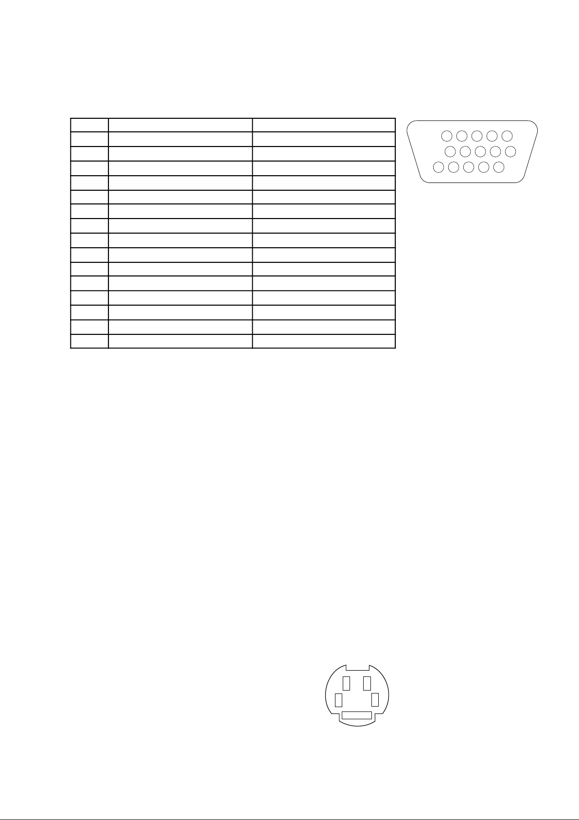
Signal layout
Pin No. Analog Signal Digital Signal
1 Analog Red N.C.
2 Analog Green Digital Green
3 Analog Blue Digital Blue
4 N.C. Digital Secondary Red(r)
5 N.C. Digital Red
6 Analog Red Return Digital Red Return(GND)
7 Analog Green Return Digital Green Return(GND)
8 Analog Blue Return Digital Blue Return(GND)
9 Test 1(Macintosh) N.C.
10 Test 2(GND) Test 2(N.C.)
11 GND GND
12 N.C. Digital Secondary Green(g,I)
13 Hsync/Csync Hsync
14 Vsync Vsync
15 N.C. Digital Secondary Blue(b.Video)
12345
678910
1112131415
Connector :Mini D-Sub 15-pin connector
JST EKHEY-15S-IF3P14-143
(applicable plug housing : JST KEC-15P)
Test 1 :When connecting to Apple Macintosh computer, this terminal must be
grounded.
Test 2 :This terminal must be grounded when inputting analog-type computer
signals.
Leave this terminal open(N.C.) when inputting digital computer signals.
2.2.Composite video signal input section
Connector :Pin jack (EIAJ RC-6703A)
2.3.Audio signal input section
Connector :Pin jack (EIAJ RC-6703A)
2.4.Power input section
Input pin :HEC0470-01-640 [Hoshiden Co., Ltd.] or equivalent
Center pin +
AC adaptor :Accessory AC adaptor DADP-2004PAZZ
Input voltage :DC12V (when main body is loaded)
2.5.S-terminal video signal input section
Signal layout : 1.GND
2.GND
3.Y signal
4
2
3
1
4.C signal
3
Page 5
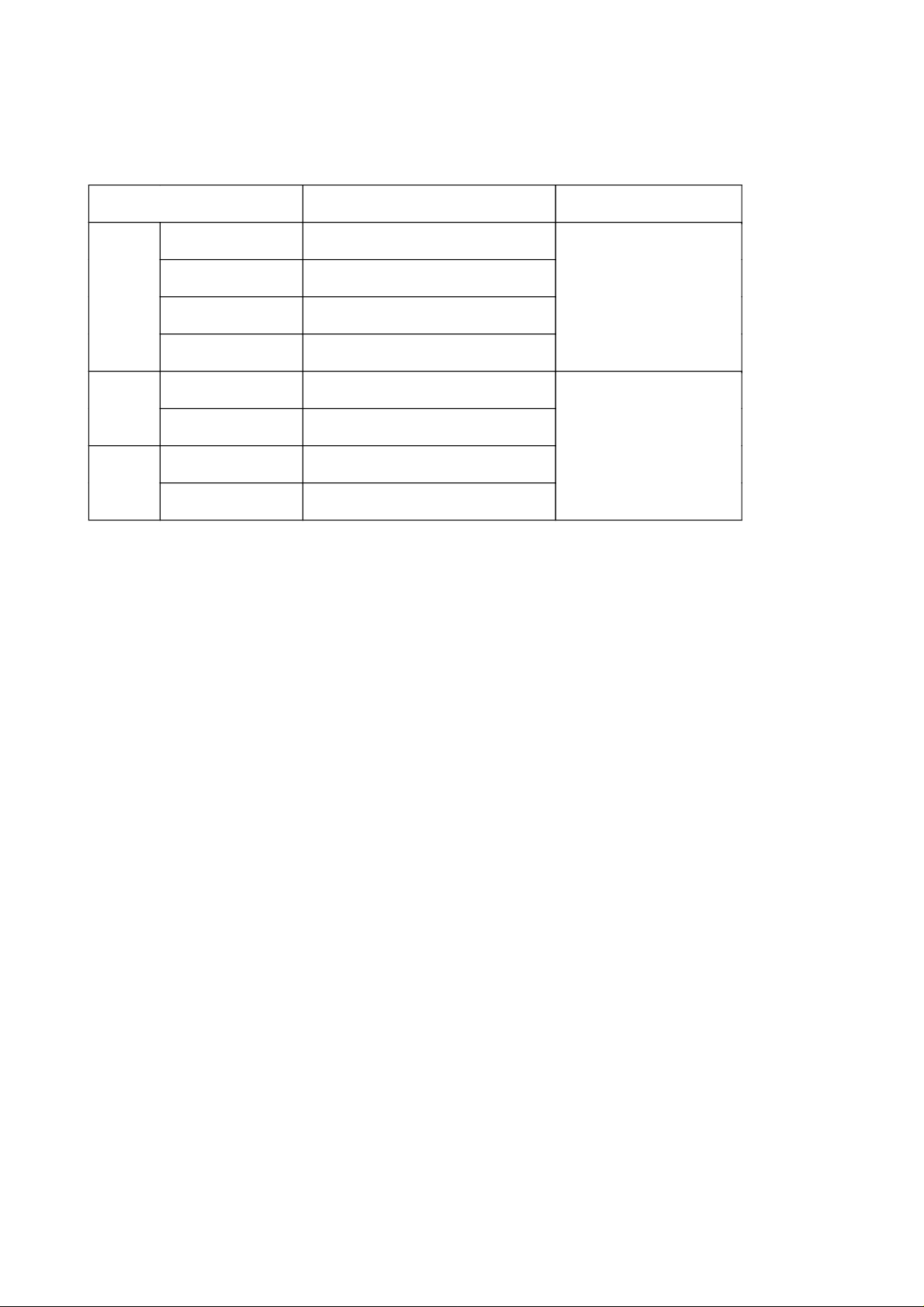
3.SPECIFICATIONS OF ENVIRONMENT
Basically, these environment specifications apply to the main body and its accessories.
Item Specification Remark
Type Single-phase 2-wire type, 1 ground line
Power
Operation
Storage
Frequency 50 / 60 Hz
Input voltage AC 100~240V
Output voltage DC 11.5 ~ 13.8V
Operating temperature 0 ~ 35 °C
Operating humidity 20 ~ 80 %RH
Storage temperature -20 ~ 60 °C
Storage humidity 20 ~ 80 %RH
Special AC adaptor accessory is
used.
Without dew condensation.
Absolute humidity shall be less
than 35 °C / 80 % RH.
4
Page 6

3. ADJUSTMENT OF PWB
The QD-101MM has a Main printed-wiring board (PWB) that needs to be adjusted.
The following paragraphs describe how to adjust the Main PWB. Correct adjustments are
essential for the unit to operate properly. After repair or maintenance, it is necessary to readjust
them. Before adjusting the control block, be sure to verify that the power supply block is
adjusted, and then adjust the control block.
1. ADJUSTMENT OF POWER SUPPLY BLOCK
There are two power voltage adjusting points: VR1 for V
, VR2 for V
CPU
LCD
.
1) Connect the AC adaptor connector plug to J1.
Verify that the output of AC adaptor approximates 12V.
2) Before turning on the power switch, check the conductive pattern on the rear of the
PWB for defects or foreign material that may short the conductive paths.
3) Turn on the power switch SW1 to verify that the LED lights.
4) V
adjustment
CPU
Connect the + lead of DC voltmeter to TP203, and the - lead to TP206.
While turning VR1 with a flat-tipped screwdriver, observe the voltmeter.
Adjust the voltage to 5.15 ±0.05V.
5) VCC voltage check
Connect the + lead of the DC voltmeter to TP202. Verify the voltage of 4.90 to 5.15V.
6) V
adjustment
LCD
Connect the + lead of the DC voltmeter to TP200.
While turning VR2 with a flat-tipped screwdriver, observe the voltmeter.
Adjust the voltage to 5.05 ±0.05V.
7) +10V voltage check
Connect the + lead of the DC voltmeter to TP204. Verify the voltage of 10±0.5V.
2.ADJUSTMENT OF CONTROL BLOCK
2.1.Offset adjustment of computer signal input amplifier
1) Turn off the power, and connect TP10 and TP303 to the DC voltmeter.
(Connect the earth terminal of the probe to TP10.)
2) Input the signal of Fig. 1-B to J2.
3) Turn on the power. Observing the DC voltmeter, adjust the TP303 level to 1.15±0.05V
by turning VR303 with the flat-tipped screwdriver.
2.2.Gain adjustment of computer signal input amplifier
1) Turn off the power, and connect TP303 and TP300 to an oscilloscope.
(Connect the earth terminal of the probe to TP10.)
2) Input the signal of Fig. 1-C to J2.
3) Turn on the power. Observing the oscilloscope, adjust the TP303 level to be equal
to TP300 level by turning VR300 with the flat-tipped screwdriver.
(Output voltage is approx.3.8V at TP300.)
4) Turn off the power, and reconnect the probe from TP303 to TP304.
5) Turn on the power. Observing the oscilloscope, adjust the TP304 level to be equal
to TP300 level by turning VR301 with the flat-tipped screwdriver.
6) Turn off the power, and reconnect the probe from T304 to TP305.
5
Page 7
7) Turn on the power. Observing the oscilloscope, adjust the TP305 level to be equal
to TP300 level by turning VR302 with the flat-tipped screwdriver.
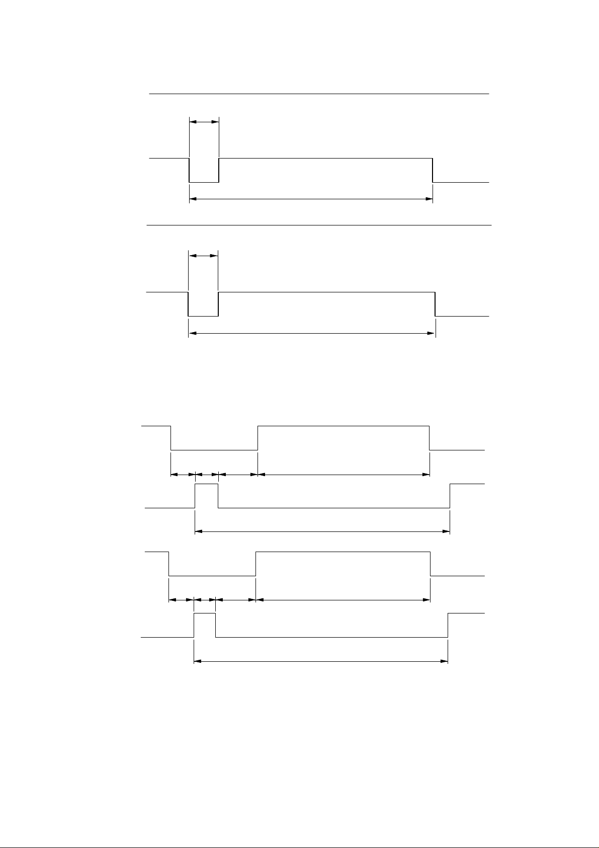
2.3.VCO adjustment
1) Connect the + lead of the DC voltmeter to TP207, and the - lead to TP10.
2) Input the video timing of Fig. 1-A to J2.
3) After turning on the power, leave it as it is for approx. 3 minutes.
Then turn L200 with ceramic driver to adjust the voltage of TP207 to 2.5±0.2V. (*1)
4) Input the video timing of Fig. 1-B or C to J2 .
5) Then turn L201 with ceramic driver to adjust the voltage of TP207 to 4.1±0.05V. (*2)
(*1) Since the voltage of TP207 varies depending on the material of the driver used,
keep the driver away from the core when checking the voltage.
(*2) It is factory-adjusted at the timing of PC9801 640X400 at shipment.
2.4.Audio speaker level adjustment
1) Input the 1KHz, 500mV(RMS) sine wave from an oscillator to the audio signal input
terminal CN502.(The audio signal level should be adjusted when power switch of QD 101MM is on.)
2) Set the volume level to maximum and the audio mute switch to off.
3) Connect an effective value type AC voltmeter to TP502 and adjust the voltage of TP504
to 2.85V(RMS) by turning VR501 with the flat-tipped screw driver.
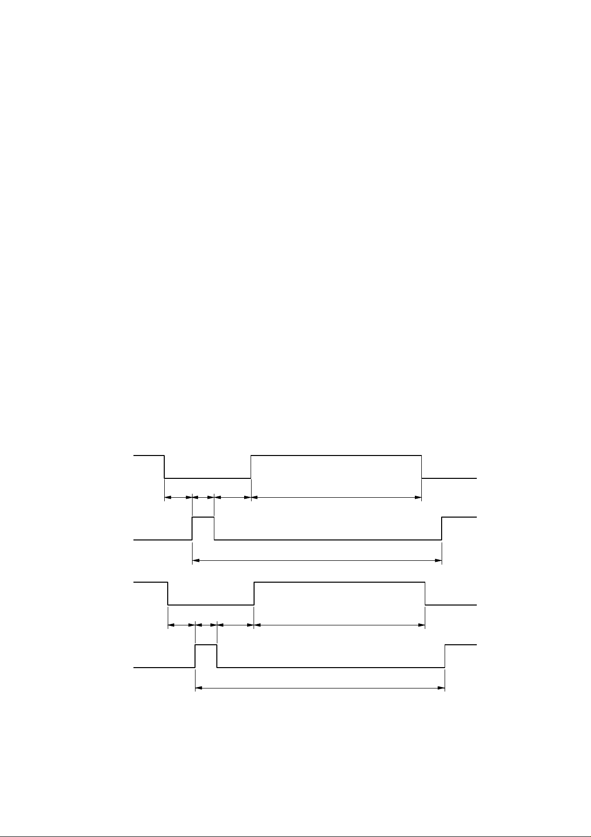
Video
Hsync
Video
Vsync
95 64 113 640dot
1H=912dot=63.696047µs
(1/H=15.699561KHz)
25 3 34 200H
1V=262H=16.688364ms
(1/V=59.92Hz)
Fig. 1-A IBM CGA 200-line 40-character
6
Page 8
Video
Hsync
0V
96
1H=800dot=31.777557µs
Video
Vsync
Video
2
16 96 48
(1/H=31.468881KHz)
0V
1V=525H=16.683217ms
(1/V=59.94Hz)
Fig. 1-B IBM VGA 480-line Black-solid
0.7V
0V
640dot
Hsync
Video
Vsync
1H=800dot=31.777557µs
(1/H=31.468881kHz)
0.7V
0V
11 2 32 480H
1V=525H=16.683217ms
(1/V=59.94Hz)
Fig. 1-C IBM VGA 480-line
7
Page 9

4. CIRCUIT DESCRIPTION
1. GENERAL
Circuit will be described in reference to the QD-101MM block diagram in Fig. 2.
Composite video signal which enters via pin jack connector is converted into the digital RGB
in the composite video input circuit by the control signal from the I2C bus controller. The signal
then enters the signal selector circuit.
Computer analog signal enters via the 15-pin connector and is processed through the computer
analog input circuit and the A/D conversion circuit. The signal is then converted into the digital
RGB signal and enters the signal selector circuit.
Digital video signal from IBM PC EGA or CGA enters via the 15-pin connector is input into the
signal selector circuit.
The signal selected in the signal selector circuit is written into the field memory. The writing
operation into the field memory is controlled by signals which are generated in the IC100 by
HSYNC. VSYNC. Since the LCD control is asynchronous with the computer signal, FRCK.
FRRS is generated in the IC100, and is read out at their timings.
The audio control circuit controls the audio signal input from the audio input terminal, according
to the control signal from IC100. IC400(MPU) controls IC100, IC107 (I2C bus controller) by the
key operation from SW PWB. Since control data from the key is stored into EEPROM, the set
data is memorized even if the power is turned off.
2. COMPUTER SIGNAL INPUT CIRCUIT
In addition to composite video signal, QD-101MM can receive the computer analog RGB signal
and the computer digital RGB signals of MDA, CGA, EGA. These signals enter each input
circuit via the 15-pin connector (J2), pin jack (CN600), and S-terminal(CN601). After they are
converted into the digital signals, they are input to the signal selector or directly to the signal
selector circuit.
Refer to MAIN CIRCUIT No.3.
2.1.Computer digital signal input circuit
The computer digital signal is input to Pins 2, 3, 4, 5, 12 and 15 of J2, and is directly sent to the
signal selector.
EGA outputs the video signal at the 6-bit TTL level. (R, G, B, r, g, b)
CGA outputs the video signal at the 4-bit TTL level. (R, G, B ,I)
MDA outputs the video signal at the 2-bit TTL level. (Mono, Video, I)
As basic, the pins of J2 output the following signals.
Table 1
Connector J2's Pin Number
Signal
12 15 4 2 5 3 14 13 11
EGA g b r G R B Vsync Hsync GND
CGA I x x G R B Vsync Hsync GND
MDA I MONO x x x x Vsync Hsync GND
x:Don`t care or N.C.
8
Page 10
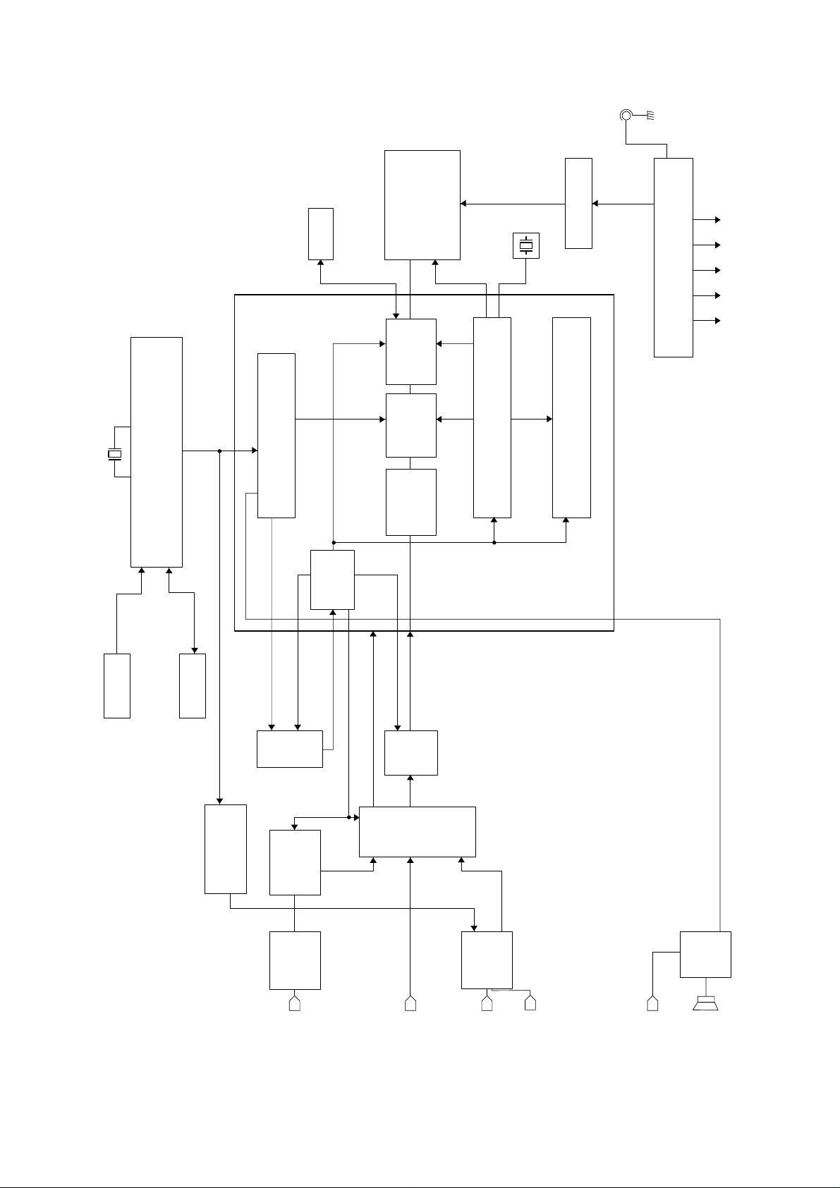
AC
J1
DC INPUT
HV
IC400
MPU
GATE ARRAY IC100
DATA REGISTER
IC108,111
VRAM
FIELD
MEMORY
WRITE
CONTROLLER
TFT COLOR LCD UNIT
MENU
CONTROLLER
MASK
CONTROLLER
COLOR
CONTROLLER
INVERTER PWB
OSC1,2
POWER SUPPLY
+10V VLCD AVCC DVCCVCPU
LCD CONTROLLER
FIELD MEMORY READ CONTROLLER
Fig. 2 QD-101MM Block Diagram
SW
CIRCUIT
IC413,414
2
E PROM
IC107
2
I C BUS
CONTROLLER
IC202,203
IC315~317
IC300~302
A/D
COMPUTER
J2
PDB
VCOIN
PLL
CLK
CONVERSION
CIRCUIT
ANALOG
INPUT
CIRCUIT
RGB SIGNAL
COMPUTER ANALOG
FIELD
MEMORY
IC103~105
SELECTOR
SIGNAL
IC600,601
J2
RGB SIGNAL
COMPUTER DIGITAL
IC308~313
COMPOSITE
VIDEO
INPUT
CIRCUIT
CN600
COMPOSITE
VIDEO SIGNAL
CN601
S-VIDEO
SIGNAL
CN502
SIGNAL
AUDIO INPUT
AUDIO
SP500
COTROL
CIRCUIT
SP
9
Page 11

2.2.Computer analog signal input circuit
IBM computer and APPLE computer output the following analog signals at the load of 75Ω.
Table 2
Computer Analog Signal
R G B
IBM 0.7Vp-p 0.7Vp-p 0.7Vp-p
APPLE 0.7Vp-p
1.0Vp-p
(Synchronization signal
overlapped)
0.7Vp-p
The signals are converted into 8-bit digital signals by the A/D converter(IC315~317).
The computer analog signals are given to Pin 21 of the A/D converter, are divided by 256
between the voltages given to Pin 18(VRT) and Pin 24(VRB), and are digitally converted.
The following table shows the reference voltage which is given to the A/D converter.
Table 3
VRT VRB
Threshold
Level
3.8V(2.8~4.8V)
Adjustment are possible
1.0V
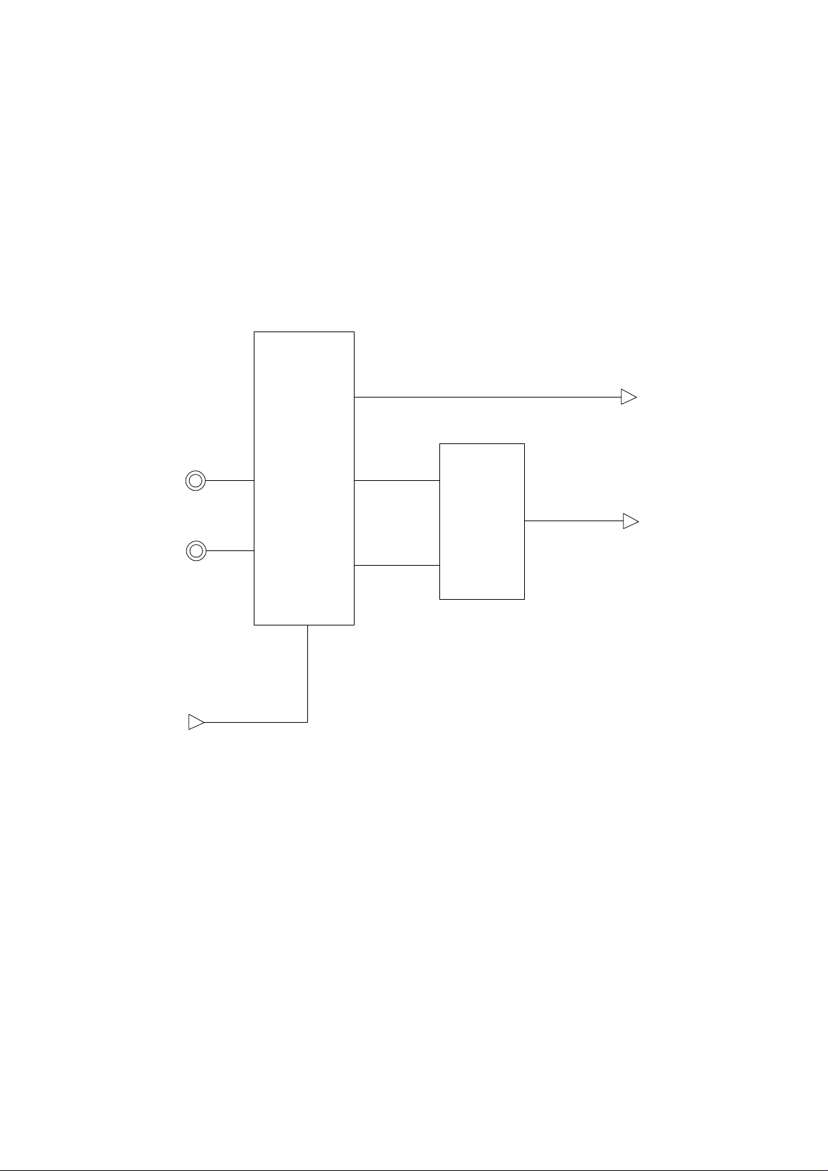
2.3.Threshold level generation circuit
In order to convert the computer and composite analog signal into digital, it is necessary to set
the threshold level on the A/D converter. As shown in Fig. 3, VRT and VRB voltages are set
on the basis of the reference power of ZD1. VRT can be varied by key operation.
As the adjusting method from the main body, the MENU button and SELECT button are used
to display the contrast adjustment in the screen and to allow the set value to be changed with
UP and DOWN selector buttons.
Fig. 3 Threshold Level Generation Circuit
10
Page 12
3.VIDEO INPUT CIRCUIT
Fig. 4 shows the block diagram. Circuit diagram is shown in VIDEO CIRCUIT.
This unit automatically switches the circuit corresponding to the composite video signals of
NTSC, PAL and SECAM. The composite video signal and S-Video signal input to the decoder
are first converted into the 8-bit digital Y,UV signal, and is output as the 8-bit digital RGB from
the RGB converter(IC601).
Horizontal sync signal CSHSYNC, vertical sync signal CSVSYNC, ODEV signal and system
clock LLC2 are simultaneously output from the decoder(IC600), and are used in the process
circuit in the rear step.
Controls of brightness, color and tint, and the initial setting of decoder and RGB converter are
sent from MPU by the I2C bus.
38,41
30
COMPOSITE VIDEO
CN600
S-VIDEO
CN601
17,19
21
DECODER
IC600
SAA7110
40
45~50
53~62
CONTROL
29
31
42
32
Y,UV
8bit
16,17,
20~25
63
64
65
26
Y,UV/RGB
CONVERTER
IC601
SAA7192
30~34,37~39
40~47
48~50,53~57
CSHSYNC
CSVSYNC
LLC2
ODEV
RGB 8bit
5,6
2
I C BUS
SDA,SCL
Fig. 4 Composite Video / S-Video Input Circuit Block Diagram
4.AUDIO INPUT CIRCUIT
Fig. 5 shows the block diagram of the audio input circuit. Circuit diagram is shown in AUDIO
CIRCUIT.
The audio signal input to the audio input terminal is inputted to the audio level controller, and
is controlled to the level which corresponds to the volume signal output from MPU.
The output enters the mute switch circuit in the next step, and the audio signal is turned on and
off corresponding to the SMUTE signal which is output from MPU.
11
Page 13
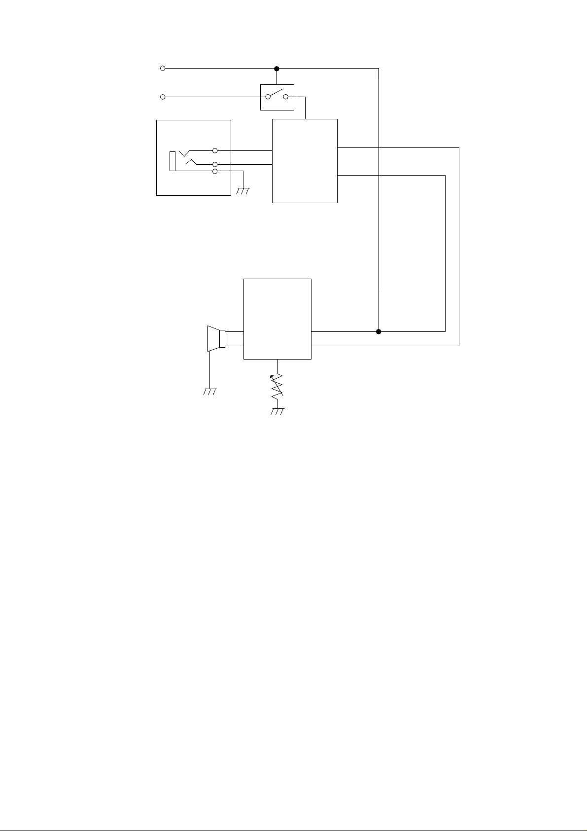
SMUTE
VOLUME
PHONE JACK STEREO INPUT
CN502
SPEAKER
SP500
MUTE SW
1
2
VR501
2
CONTOROLLER
IC503
TDA1905
AMPLIFIER
AUDIO
LEVEL
IC500
TA8184F
4
5
SPEAKER
AMPLIFIER
ADJUST
7
24
Fig. 5 Audio Input Circuit Block Diagram
5. PLL CIRCUIT
The dot clock (VCOIN) is generated by the PLL circuit shown in Fig.6. The dot clock is necessary
to sample the video signal from the computer and change it into the suitable dot data.
Hsync signal from computer enters into IC100. This signal is compared frequency and phase
with the feed-back signal, which is generated from VCOIN by the phase comparator in IC100.
If any error of phase or frequency occurs between Hsync and VCOIN, LOW or HIGH level is
output at PBD of IC100, and when both frequency and phase agree with each other, high
impedance is output.
The output signal from the PDB terminal is converted into a DC voltage by a loop filter and then
controls the VCO.
To select the high band or low band, either VCO is selected according to the signals from No.
120 pin and No. 119 pin of IC100.
12
Page 14
Fig.6 PLL Circuit
6. MEMORY CIRCUIT
BLOCK DIAGRAM is shown in Fig.2.
6.1.Field memory writing
When data sent from the signal selector is written into the field memory(IC103~105), FWCK
(clock slightly later than CLK) generated from the memory controller in IC100 is used.
6.2.Field memory reading
The clock (FRCK) and control signals which are generated in the field memory reading signal
generating circuit in IC100 are used to read data from the field memory.
Reading is asynchronous with writing. In the ordinary mode, data written into the field memory
are color-compensated and are sent to LCD.
In the enlargement mode, the enlargement control signal is sent to the field memory from the
field memory writing/reading signal generating circuit in IC100 to make the enlargement display
possible.
6.3.Menu, message display memory
The menu and message display is stored in the ROM area of IC400(MPU).
When the menu button is first pressed, MPU will write data and address into VRAM (IC108, 111)
via IC100. Moreover, VRAM data is read via IC100.
The data is sent to LCD at the timing of LCD.
LCD
IC108, 111
VRAM
menu and
message data
IC100
display data
ROMMPU
IC103~105
FIELD MEMORY
Fig. 8 Memory Circuit Block Diagram
13
Page 15

7. VARIOUS FUNCTIONS OF IC400(H8/3256 M.P.U)
IC400 is a microcomputer which is provided with a set of 16-bit free running timer and 2
channels of SCI in addition to 48K-byte PROM/2K-byte RAM.
7.1.Key data and various functions
The keys (DOWN, UP, SELECT, MENU, RESET) provided on the main body of QD-101MM
switches and selects the adjustment mode displayed in the LCD screen as well as gives the
direct commands to IC400.
1) DOWN
This key decreases the adjustment items selected by the select key, step by step.
2) UP
Being opposite to DOWN, the key increases the adjustment item, step by step.
3) SELECT
This key is used to select the adjustment mode in the menu screen which is displayed
by the MENU key.
Every push of this key can change the adjustment item, step by step.
4) MENU
This key is used to switch the menu screen.
5) RESET
This key is used to set the initial values of the computer. When this key is pressed,
the adjustment items are all returned to the initial statuses.
7.2.EEPROM control function
The EEPROM(IC413, 414) area is provided to write the timing set values of each computer
when it is connected to QD-101MM. The timing set values are written into EEPROM under the
following four conditions.
1. All resetting
2. Resetting
3. Power turn-off
4. The connected computer is changed.
Here, writing into EEPROM is executed only when the set value is changed.
7.3.Reset circuit
The circuit diagram is shown in MAIN CURCUIT No.4.
IC407(TL7705CPS-B) detects the power voltage, V
and generates the RESET signal. If V
drops below the detection voltage (TYP4.5V) when
CPU
, of IC400 and its surrounding circuit,
CPU
the power is turned off, IC407 shifts the level of the RESET signal to “Low”.
If V
V
rises to exceed the total voltage of the detection voltage VS1 and hysteresis width
CPU
(TYP15mV), IC407 starts charging the timing capacitor(Ct) with a constant current.
HYS1
After (TP0=1.3XCtX10[S]), IC407 shifts the RESET signal to “High” level. (See Fig. 8.)
IC411(S-8054ALB) detects the power voltage VCC to generate the power OFF signal. If V
CC
drops below the detection voltage VS2 (TYP4. 15V) when the power is turned off, IC411 shifts
the power OFF detection level to “Low”.
If VCC rises beyond the total voltage of the detection voltage VS2 and hysteresis voltage V
HYS2
(TYP200mV) when the power is turned on, IC411 shifts the power OFF signal to “High” level.
(See Fig. 9.)
14
Page 16
VCPU
(4.5V)
RESET
signal
VCC
(4.15V)
V
S1
PO TPO TPO
T
VHYS1
(15mV)
Fig.8
V
S2
VHYS2
(200mV)
POWER OFF
DETECTION
signal
Fig.9
When the power is turned on, V
, VCC and V
LCD
rise. If V
CPU
exceeds VS1+V
CPU
, the RESET
HYS1
signal is shifted to “High” level at the timing shown in Fig. 10. The reset operation of IC400 is
canceled and executes the program.
When the power is turned off, the power OFF detection signal is shifted to “Low” when VCC and
V
drops sharply below VS2.
LCD
On the other hand, Vcpu is backed up by C425 (220mF) so that it can maintain 4.5V for the time
of TW after the trailing edge of the power OFF detection signal. See Fig. 11. (TW is the time
for IC400 to retreat the data to EEPROM.) If V
drops below VS1, the RESET signal level is
CPU
shifted to “Low”, and IC400 starts resetting.
15
Page 17
VS1(VCPU)
S2(VCC)
V
POWER OFF
DETECTION
signal
VCPU
VCC
RESET
5.0V
VS1(4.5V)
4.0V
POWER OFF
DETECTION
signal
TPO
Fig.10
VCPU
V
S2
VCC
TW
RESET
Fig.11
16
Page 18
8. LCD CONTROL CIRCUIT
LCD control signal is slower than the video signal of the computer. While the video signal is
serial data, the LCD display data is given as 4-bit parallel data for each RGB. In order to display
the bit signal of the computer in LCD, it is necessary to store the data of one screen in the
memory and read out the image data of one screen at the drive timing of LCD. To control them,
the field memory is controlled by the memory controller in IC100 as shown in the block diagram
in Fig. 2.
9. LCD UNIT
9.1.Interface signals
3 1
22 20 18 16 14 12 10 8 6 4 2
CN1 Pin assignment
Table 4 Pin assignment of LCD unit
Pin Code Function Remark
1 GND
2 CK Sampling clock signal of data
3 Hsymc Horizontally synchronous signal (*1)
4 Vsync Vertically synchronous signal (*1)
5 GND
6 R0 Red data signal(LSB)
7 R1 Red data signal
8 R2 Red data signal
9 R3 Red data signal
10 R4 Red data signal
11 R5 Red data signal(MSB)
12 GND
13 G0 Green data signal(LSB)
14 G1 Green data signal
15 G2 Green data signal
16 G3 Green data signal
17 G4 Green data signal
18 G5 Green data signal(MSB)
19 GND
20 B0 Blue fata signal(LSB)
21 B1 Blue fata signal
22 B2 Blue fata signal
23 B3 Blue fata signal
24 B4 Blue fata signal
25 B5 Blue fata signal(MSB)
26 GND
27 ENAB Data enable signal(Horizontal display position signal) (*2)
28 Vcc +5V power suppry
29 Vcc +5V power suppry
30 TST Open
31 TST Open
24
29 27 25 23 21 19 17 15 13 11 9 7 5
31
30
28 26
The shield case is connected to GND in LCD module.
(*1) The line mode(480 or 400 or 350) can be selected by the polarity of Hsync and Vsync.
Mode 480line 400line 350line
Hsync Negative Negative Positive
Vsync Negative Positive Negative
(*2) Don't use "High".
17
Page 19
9.2.Sequence circuit of LCD panel
In QD-101MM, it is necessary to conform the power ON/OFF sequence of the LCD panel as
shown Fig.12.
LCD
V
T1 T2
Signal
0 T1
0 T2
Fig. 12 Power ON/OFF sequence
Fig. 13 shows the panel sequence generation circuit.
The gate signal which has the same timing as the input signal in Fig. 12 is output by the RESET
IC of IC4 and IC5.
Fig. 13 Panel Sequence Generation Circuit
9.3.Handling the LCD panel
1. The LCD unit is assembled to very high density, do not attempt to disassemble it.
2. The polarizing plate is very easy to scratch, take extra care when handling it.
3. When cleaning the surface of the LCD panel, use absorbent cotton or soft cloth and
carefully wipe the surface.
4. The LCD panel will become discolored or stained if any moisture remains on the surface
for a long period of time.
5. The LCD panel is made of glass. If it is hit by any hard object or is dropped, it may
crack.Handle it very carefully.
6. CMOS LSI which is used in the LCD unit is very sensitive to static electricity. To prevent
damage to the LCD unit from static electricity it is necessary for all service technicians
to use a conductive mat and wrist strap to ground themselves when servicing the unit.
10.POWER CIRCUIT
The AC adaptor which is connected to QD-101MM supplies stable power to the unit, and
generates 5V power (VCC, V
power(12V).
CPU
, V
), VPP power, +10V power and the inverter circuit board
LCD
18
Page 20
10.1. +5V power (VCC, V
CPU
, V
LCD
)
IC1 in Fig. 14 is a controller for a fixed frequency pulse width modulation(PWM) switching
regulator and has two constant voltage controllers. One controller is used to generate a 5V
power supply(V
CPU,VCC
) from the input power supply VIN(12VDC). The other one is for V
LCD
IC1 has a saw-tooth wave oscillator built in whose oscillating frequency is determined by
capacitor C30 connected to pin 1 and resister R29 connected to pin2. In this circuit
configuration, a saw-tooth wave of approx.75KHz is observed at pin 1 of IC1. Basically this sawtooth wave is compared with a control signal observed at pin5 of IC1. Only while the voltage
of the saw-tooth wave is lower than the control signal voltage, the period between pin 7 of IC1
is "L" becomes longer. As a result the period between external transistor Q11 and Q10 is
conductive becomes longer. The output voltage is fed back to pin 3 of IC1. An error amplifier
in IC1 makes a comparison between the half of the reference voltage and the feed-back signal
to pin 3 and generates a control signal(pin5 of IC1). As explained above the output voltage is
stabilized by the pulse width from pin 7, which is generated by comparing the control signal with
the saw-tooth wave.
V
is adjusted to 5.1V while VCC is 5V. This is done because the load on the VCC is greater than
CPU
the load on V
and the forward voltages of D8, D9, and D10 are higher than that of D7.The
CPU
voltage supplied to pin 6 of IC1 is called a dead time control signal. It controls the maximum
ON period of the output transistor in IC1. The maximum ON period is realized on IC1 by shorting
pin 6 and pin 16.
The saw-tooth wave oscillator of pin 1 of IC1 is used also for the control of this 5V power
supply(V
). The operation of the circuit is similar to that of the other 5V power supply(V
LCD
CPU
and
VCC). The output voltage is fed back to pin 14 of IC1. The control signal is produced using a
voltage generated by dividing the reference voltage inputted to pin 13 of IC1, and the feed back
signal. The output voltage is stabilized by the pulse width from pin 10, which is generated by
comparing the control signal with the saw-tooth wave. V
is adjusted to 5.0V with VR2.
LCD
.
Fig. 14 +5V Power(VCC,V
19
CPU,VLCD
) Circuit
Page 21

10.2. +10V power
Fig. 15 shows the +10V power supply.
+10V is generated from the input power supply of 12V by the 3-terminal regulator of IC7.
Fig.15 +10V Power Circuit
1 1. INVERTER CIRCUIT
The Inverter circuit board supplies the high voltage AC to the cold-cathode fluorescent tube
used as backlight illumination for the TFT panel.
The Inverter circuit is supplied the voltage from CN20 on the Main PWB and it gives to the coldcathode fluorescent tube. The lighting level control can be varied by turning VR50.
(Note)
(1) Inverter circuit is very dengerous because it is outputted the high voltage(max AC1300V).
Make sure that the monitor's power switch is in the OFF position when servicing Inverter
circuit board.
(2) Inverter circuit board can not be replaced. It needs to be replaced when it is failed.
20
Page 22

START
5. TROUBLESHOOTING CHART
Yes
POWER ON
Is the LED
illuminated?
Yes
Is the backlight
illuminated?
Yes
Push the RESET
button.
No
No
Is CN20 12V?
Yes
Is the voltage at the both
side of fuse on the Inverter
circuit board 12V?
Yes
Backlight failure.
No
No
No
Inverter circuit board
failure.
Is power supply voltage
described (*1)?
Yes
1
No
(*1)
TP1 =approx.12V
TP200=approx.5V
TP202=approx.5.1V
TP203=approx.5.15V
TP204=approx.10V
21
Go to Power Source
Circuit Check.
Page 23

Power Source Circuit
Check
POWER OFF
Is the voltage between 1-pin
and 2-pin of J1 approx.12V?
(2-pin is GND)
Yes
POWER ON
Is D2 cathode
approx.12V?
Yes
Is TP203(V
approx.5.15V?
Yes
CPU
)
No
No
No
AC adaptor failure.
F1 failure.
Is D7 anode
approx.5.5V?
No
Yes
D7 failure.
Is TP202(VCC)
approx.5.1V?
Yes
Is TP200(V
approx.5V?
Yes
Is TP204(+10V)
approx.10V?
Yes
Go to Another
Function Check.
LCD
No
)
No
No
Failure of IC7 or their
peripheral parts.
D8,D9,D10 failure.
Disconnect the LCD unit
from CN100.
Is TP200(V
approx.5V?
No
LCD
)
LCD unit failure.
Yes
Failure of IC1 or their
peripheral parts.
22
Page 24

1
Digital Signal Display Check
Input a digital video signal.
(CGA 14.318MHz)
87
Check IC206-6.
Is clock pulse inputted
approx.14.318MHz to
IC100-pin116
(VCOIN)?
Yes
Is proper video signal at
IC100?
Yes
Are J2-pin 9(MAC) and
10(A/D) at a high level?
Yes
No
2
No
No
Disconnect the signal cable
from J2.
IC28 failure.
Signal cable failure.
23
No
Are proper signals outputted
at signal cable-
pin5,2,3,4,12,15
(R,G,B,r,g,b,A/D)?
Yes
Digital Video Signal Input
Circuit failure.
Page 25

2
Is IC100-pin119(PVOL) at a
high level?
Is IC100-pin 120(PVOH) at a
low level?
Yes
Is Q101-collector at a low
level?
Is Q102-collector at a high
level?
Yes
Is TP207 approx.2.5V?
Yes
No
IC100 failure.
No
Q101 or Q102 failure.
No
Can TP207 be adjusted to
approx.2.5V with L200
(LOW BAND)?
Yes
Adjust TP207 to approx.2.5V
with L200.
No
Low band VCO circuit
failure.
24
Page 26

Analog Video Signal
Display Check
Input an analog video
signal.
(VGA,25.175MHz)
7 8
No
No
Check IC206-pin6.
Is clock pulse(25.175MHz)
inputted to IC100-pin 116
(VCOIN)?.
Yes
Disconnect the signal cable
from J2.
Are proper video signals at a
signal cable-pin1,2,3
(A-R,G,B)?
Yes
Is the signal cable-
pin9(MAC) open?
Is the signal cable-pin10
(A/D) GND level?
No
4
Signal cable failure.
Yes
Connect the signal
cable to J2.
Minimize the
CONTRAST.
3
25
Page 27

3
Is TP300(VRT)
approx.2.8V?
Is TP301(VRB)
approx.1V?
Yes
Maximize the
CONTRAST.
Is TP300
approx.4.8V?
Is TP301 approx.1V?
Yes
Push RESET switch to set
the CONTRAST to center.
No
No
Failure of threshold
level setting circuit.
Are amplified video
signals generated from
TP303,304, and 305?
(IC300,301,302
output)?
Yes
Is IC100-
pin108(CSYNCSP) at
a high level?
Yes
Are digitalized video
signals(TTL level) outputted
from pins-1~8 on
IC315,316,317
(A/D converter)?
Yes
No
Adjust again or failure of
IC300,301,302 or their
peripheral circuits.
No
IC100 failure.
No
Failure of IC315,316,317
or peripheral circuits.
IC100(Gate Array) failure.
26
Page 28

4
Is IC100-pin119(PVOL) at a
low level?
Is IC100-pin120(PVOH) at a
high level?
Yes
Is TP207 approx.4.1V?
Yes
Can TP207 be adjusted to
approx.4.1V with L201
(High Band)?
Yes
Adjust TP207 to approx.4.1V with
L201.
No
IC100 failure.
No
No
High band VCO circuit
failure.
27
Page 29

Composite Sync. Signal
Display Check.
Input a composite sync.
signal.
(MAC II type: 30.24MHz)
7 8
Failure of analog
threshold level setting
circuit.
Check IC206-pin6.
Is clock pulse of
approx.30.24MHz inputted to
IC100-pin116
(VCOIN)?
Yes
No
No
Is IC100-pin108 at a
low level?
Yes
Disconnect the signal cable
from J2.
Is signal cable-
pin9(MAC) shorted
to GND?
Is signal cable-pin10
(A/D) GND?
No
Is Hsync inputted to IC100-
pin109?
Is Vsync inputted to IC100-
pin110?
Yes
Is clock pulse of
approx.25.00MHz inputted to
IC100-pin19?
Yes
IC100 failure. OSC1 failure.
No
Failure of signal cable
or input circuit.
No
No
Signal cable failure.
Yes
Is proper level video signal at
signal cable-pin1,2,3?
Yes
Input circuit failure.
28
Page 30

MPU Circuit Check
Press the RESET
switch.
1
2
3
Does IC400-pin7 changed the level
from "L" to "H" after power is turned
Is clock pulse of
approx.7.987MHz at
IC400-pin2?
Yes
on?
Yes
Is IC400-pin5 and pin64 always
high after turning the power on?
Yes
No
No
No
7.987MHz oscillating circuit
failure.
Failure of reset circuit or its
peripheral circuits.
IC400 failure.
Failure of power off detection
circuit or its peripheral circuits.
IC400 failure.
4
Is clock pulse of approx.4MHz
outputted from IC400-pin15?
Yes
Go to Digital Signal
Display Check.
No
IC400 failure.
29
Page 31

LCD Display Circuit Check
Input a digital video signal.
(CGA type; 14.318MHz)
6 7 8
Yes No
Is Hsync inputted to IC100-
pin109?
Is Vsync inputted to IC100-
pin110?
Yes
5
Is clock pulse of
approx.25.00MHz at
IC100-pin19?
Yes
Is clock pulse of
approx.14.318MHz at IC206-
pin6(VCOIN)?
No
Failure of Hsync/ Vsync input circuit
No
OSC1 failure.
5
7 8
or signal cable
Do input signal to IC100-
pin110(Vsync) and output signal
from IC100-pin130(VSC) have the
same frequency?
Yes
Is IC100-pin129(F256HS)
approx.61.326Hz ?
Yes
Are the output levels from
IC100-pin126(HPOL) and
pin127(VPOL) both high?
Yes
6
No
No
No
Failure of IC100 or its
peripheral circuits.
30
Page 32

5
9 10 11
Are signals at IC100-
pin82(LHsync),
83(LVsync),and
79(LCDCK) normal?
Yes
No
No
IC100 failure.
Disconnect the panel.
Are signals at IC100-
pin82,83,and 79
normal?
Yes
Panel failure.
9 10 11
Are digital video signals inputted to
IC100-
pin5,6,95~98(B),3,4,90~93(G),and
1,2,85~88(R)?
Yes
Failure of IC100(Gate Array),
400(MPU),103~105(Field Memory).
No
Video signal input circuit failure.
31
Page 33

6
Is output level from IC100-
pin140(RESET) high?
Yes
Are proper signals at IC100-
pin132~139(KA0~7),
147~154(KD0~7)?
Yes
Is IC100-pin119(PVOL)
at a high level?
Is IC100-pin120(PVOH)
at a low level?
Yes
Is Q102-collector at a
low level?
Is Q101-collector at a
high level?
No
No
Failure of signal line
between IC100 and IC400.
No
IC100 failure.
No
Yes
Failure of VCO circuit or
pattern.
Failure of Q102 or Q101.
32
Page 34

Video Circuit Check
Input NTSC video signal to
CN600.
Are video signals inputted
to IC600-pin21?
Yes
Is a video signal outputted
from TP600?
Yes
Are Hsync or Vsync
outputted from IC600-
pin38 and pin41?
Yes
No
Input cable failure.
Input connector failure.
No
Check IC107 and 400.
No
IC600 failure.
Are digital video signals
outputted from IC601-
pin30~39,40~47,and
48~57?
Yes
Input NTSC and PAL video signal
Is IC400-pin24(XTALSL) "H"
when NTSC is inputted, "L"
when PAL is inputted?
Yes
Failure of
IC417,419,420,418.
No
IC601 failure.
No
IC400 failure.
33
Page 35

Audio Circuit Check
Input a 500mV(RMS) sine-wave to
audio input terminal.
Set the volume to maximize and
mute off.
Is the signal outputted from
IC500-pin7?
Yes
Are the signals outputted from IC507-
pin2 and IC508-pin2?
Does the signals change 0V when mute
off?
Yes
Is the signal inputted to
IC503-pin5?
No
IC500 failure
No
IC507,508 failure.
No
IC503 failure.
Yes
Is 2.85V(RMS) sine-wave
outputted from TP504?
Yes
Check speaker.
No
IC503 failure.
34
Page 36

1 IC400-2
1V/div
50ns/div
2 V
CPU...2V/div
IC400-7...2V/div
5ms/div
GND/
GND/
GND/
V
CPU
IC400-7
Fig.16
3 Vcc...2V/div
IC400-5,64
2V/div
10ms/div
4 IC400-15...1V/div
50ns/div
Fig.17
Vcc
GND/
IC400-5,64
GND/
Fig.18
GND/
Fig.19
35
Page 37

5 IC100-19
1V/div
10ns/div
6 IC100-110...2V/div
500ns/div
GND/
Fig.20
7 IC100-110...2V/div
IC206-6...2V/div
50ns/div
GND/
GND/
8 IC100-109...2V/div
IC206-6...2V/div
20ns/div
GND/
Fig.21
IC100-110
IC206-6
Fig.22
IC100-109
GND/
IC206-6
Fig.23
36
Page 38

9 IC100-79
1V/div
5ns/div
10 IC100-82
1V/div
2.5µs/div
IC100-79(LCDCK)
GND/
Fig.24
IC100-82(LHsync)
11 IC100-83
1V/div
2.5ms/div
GND/
Fig.25
IC100-83(LVsync)
GND/
Fig.26
37
Page 39

6. CIRCUIT DIAGRAM & PWB
Fig.27 CIRCUIT DIAGRAM(MAIN CIRCUIT No.1)
38
Page 40

Fig.27 CIRCUIT DIAGRAM(MAIN CIRCUIT No.1)
39
Page 41

Fig.28 CIRCUIT DIAGRAM(MAIN CIRCUIT No.2)
40
Page 42

Fig.28 CIRCUIT DIAGRAM(MAIN CIRCUIT No.2)
41
Page 43

Fig.29 CIRCUIT DIAGRAM(MAIN CIRCUIT No.3)
42
Page 44

Fig.29 CIRCUIT DIAGRAM(MAIN CIRCUIT No.3)
43
Page 45

Fig.30 CIRCUIT DIAGRAM(MAIN CIRCUIT No.4)
44
Page 46

Fig.30 CIRCUIT DIAGRAM(MAIN CIRCUIT No.4)
45
Page 47

Fig.31 CIRCUIT DIAGRAM(POWER CIRCUIT)
46
Page 48

Fig.31 CIRCUIT DIAGRAM(POWER CIRCUIT)
47
Page 49

Fig.32 CIRCUIT DIAGRAM(VIDEO CIRCUIT)
48
Page 50

Fig.32 CIRCUIT DIAGRAM(VIDEO CIRCUIT)
49
Page 51

Fig.33 CIRCUIT DIAGRAM(AUDIO CIRCUIT)
50
Page 52

Fig.33 CIRCUIT DIAGRAM(AUDIO CIRCUIT)
51
Page 53

(FRONT-SIDE)
Fig.34 PWB PATTERN(MAIN PWB)
52
Page 54

(REAR-SIDE)
Fig.34 PWB PATTERN(MAIN PWB)
53
Page 55

7. REPLACEMENT PARTS LIST
"HOW TO ORDER REPLACEMENT PARTS"
To have your order filled promptly and correctly,
please furnish the following information.
1.MODEL NUMBER
3.PART NO.
No. REF.No. PART CODE NEW DESCRIPTION QTY PRICE
1. MAIN PWB ASSEMBLY(DPWB-2146YAZZ)
1-1. IC
1 IC1 RH-IX1234PAZZ uPC1100GS(T) 1 AL
2 IC4,407 RH-IX0855PAZZ TL7705CPS-B 2 AK
3 IC5 RH-IX2788YAZZ PST529C 1 AG
4 IC7 RH-IX2936YAZZ uPC24M10HF 1 AH
5 IC22,23 RH-IX0853PAZZ TL712CPS-A 2 AQ
6 IC28 RH-IX2661YAZZ TC74HC04AF EL 1 AD
7 IC100 RH-IX2893YAZZ L7A1322(GATE ARRAY) 1 BF
8 IC101 RH-IX2872YAZZ 74VHC08F 1 AD
IC102,314,405,406,410,
9
421,422,509
RH-IX2650YAZZ TC7S04 8 AC
10 IC103-105 RH-IX2926YAZZ HM530281-20 3 BH
11 IC106 RH-IX2921YAZZ CE16V8(PLD1502) 1 AQ
12 IC107 RH-IX2896YAZZ PCF8584 1 AZ
13 IC108,111 RH-IX2919YAZZ IS62C256-70U 2 AV
14 IC200 RH-IX1233PAZZ TL750L10LP 1 AM
15 IC201 RH-IX2866YAZZ MB88346B 1 AS
16 IC202,203 RH-IX1235PAZZ SP1648(T) 2 AT
17 IC204,206,416 RH-IX1239PAZZ MM74HC00(T) 3 AE
18 IC205 RH-IX1236PAZZ TLC27L9C(T) 1 AR
19 IC300-302 RH-IX2818YAZZ LM1201M 3 AW
20 IC307-313 RH-IX2899YAZZ 74ACT374(SSOP) 7 AQ
21 IC315-317 RH-IX2927YAZZ CXD2302Q 3 BC
22 IC400 RH-IX2979YAZZ N HD6473256F10 1 BF
23 IC401-403 RH-IX2910YAZZ 74HC245 3 AH
24 IC404 RH-IX1922PAZZ TC74HC32AF-EL 1 AD
25 IC409,415,420,512 RH-IX2832YAZZ TC7S08F 4 AC
26 IC411 RH-IX0847PAZZ S-8054ALB-LM-TI 1 AF
27 IC413,414 RH-IX2897YAZZ 35C116 2 AV
28 IC417 RH-IX2917YAZZ TC7S86 1 AE
29 IC418 RH-IX2857YAZZ TC74HC221AF 1 AH
30 IC419 RH-IX1133PAZZ SN74LS74ANS 1 AE
31 IC500 RH-IX2890YAZZ TA8184F 1 AN
32 IC503 RH-IX2892YAZZ TDA1905 1 AL
33 IC507,508 RH-IX2925YAZZ 7S66 2 AF
34 IC600 RH-IX2888YAZZ SAA7110 1 BQ
35 IC601 RH-IX2889YAZZ SAA7192A 1 BQ
1-2. DIODE
1 D2,7-10 VHD1S1885//-1 1S1885 5 AB
2 D3,4 VHDSB05-05CP1 SB05-05CP 2 AC
3 D6,11 VHDERB81-004/ ERB81-004 2 AE
4 D200-202 VHD1SS294//-1 1SS294(A9) 3 AA
5 D203 VHD1SV211//-1 1SV211 1 AB
6 D204 VHDKV1230Z/-1 KV1230Z 1 AH
7 D205,300-302 VHD1SS226//-1 1SS226(C3) 4 AB
8 D502 VHERD10M///-1 RD10M 1 AD
9 D700,800,802 VHD1SS193//-1 1SS193 3 AA
10 D801 VHERD15MB3/-1 ERD15MB3 1 AB
11 DA400,401 VHDHN2D01F/-1 HN2D01F(T) 2 AC
12 ZD1 VHELM385BX/-1 LM385BX 1 AV
2.REF.NO.
4.DESCRIPTION
54
Page 56

No. REF.No. PART CODE NEW DESCRIPTION QTY PRICE
1-3. TRANSISTER
1 Q8,11 VS2SA1182-Y-1 2SA1182-Y 2 AB
2 Q9,10 VS2SA1293Y/1E 2SA1293Y 2 AG
3 Q101,102,500 VS2SC3913//-1 2SC3913-TB 3 AB
4 Q200 VSHN1C01FY/-1 HN1C01F-Y(T) 1 AB
5 Q201,702 VS2SA1162SY-1 2SA1162-SY 2 AA
6 Q202,203 VSFP1A3M///-1 FP1A3M(T) 2 AC
7 Q204 VS2SA1204RY-1 2SA1204RY 1 AC
8 Q205 VS2SC2884PY-1 2SC2884PY 1 AC
9 Q701 VSDTC-144WK-1 N DTC144WK 1 AC
10 Q800,801 VS2SC2712LY-1 2SC2712 LY 2 AA
1-4. COIL
1 L7,10,13 RCILZ3877PAZZ RCR-875D 22MH 3 AE
2 L8,9,11,12 RCILZ3878PAZZ RCR-110D 270MH 4 AF
3 L14 RCILZ2109YAZZ RCH-664 100MH 1 AD
4 L200 RCILZ3875PAZZ 7KTLT 2.45MH 1 AD
5 L201 RCILZ2135YAZZ 7KTLT 0.15UH 1 AE
6 L600,601,603 RCILZ2133YAZZ NW5650(10MH) 3 AH
7 L602 VP-VD100K0000 LEM4532 10MH 1 AC
8 L800 RTRNZ0035PAZZ FILTER-COIL 1 AE
1-5. FILTER
1 FL100 RMPT-2062YAZZ ACF321825-470 1 AE
2 FL102 RFILN2002YAZZ NFM840R01G101 1 AD
3 FL200,201,203-206 RFILN0163PAZZ NFM61R10T102 6 AE
4 FL800 RCILZ2110YAZZ PLT1R53C 1 AH
5 FL801 RCORF0058PAZZ BNX002-01 1 AD
1-6. CORE
1 FB100-119 RCORF2024YAZZ BLM11A12 20 AC
2 FB120,130,300,301 RCORF2044YAZZ N BLM21A50 4 AC
3 FB122,L202,203 RCORF2011YAZZ BLM41A04 3 AE
FB123,124,126,132,13
4
4,302-304
5 FB125 RCORF2023YAZZ MMZ2012S181A 1 AB
6 FB127 RCORF2038YAZZ N BLM11B30 1 AC
7 FB131 VRN-CY1JQ561D (CY)1/16W-560D 1 AA
8 FB133 RCORF2010YAZZ BLM21A05 1 AE
9 FB202 RCORF2033YAZZ BLM21B30 1 AC
10 FB204-206 RCORF2027YAZZ BLM21A10 3 AC
1-7. OSCILLATOR
1 OSC1 RCRS-2123YAZZ DSO751S 25.175 1 AV
2 OSC2 RCRS-2124YAZZ DSO751S 21.000 1 AT
3 XTL400 RCRS-2129YAZZ AT-51 7.9872MHZ 1 AS
4 XTL600 RCRS-2127YAZZ 9922 520 30004 1 AL
1-8. LED
1 LED1 RH-PX2157YAZZ N LED(RED)TLR206 1 AC
1-9. RELAY
1 RL1 RRLY-2124YAZZ RELAY JY-12H-K 1 AM
2 RL2 RRLYU0090PAZZ A-12W-K 1 AT
1-10. VR
1 VR1,2 RVR-M2276YAZZ RVG4M08(2KORM) 2 AF
2 VR50,51 RVR-M2294YAZZ N RK08H-50K 2 AH
3 VR300-302 RVR-M0216PAZZ VR ST-4 5K 3 AG
4 VR303 RVR-M2285YAZZ ST-4A 1K 1 AG
5 VR501 RVR-M2290YAZZ ST-4A 20K 1 AH
1-11. FUSE, FUSE HOLDER
1 F1 QFS-F0003PAZZ FUSE 2A/125V 1 AD
2 QFSHA2008YAZZ 85PE1850 2 AA
RCORF2030YAZZ BLM11B20 8 AC
55
Page 57

No. REF.No. PART CODE NEW DESCRIPTION QTY PRICE
1-12. JUMPER, JACK, CONNECTOR
1 JAG1.JDG1 QJUM-3001CEFW N 5M/M-JUMPER 2 AB
2 J1 QSOCZ0115PAZZ DC JACK 1 AC
3 J2 QPLGJ2731YAZZ D-SUB 15P 1 AX
4 CN20 QPLGJ2755YAZZ N DF13-5P-1.25DSA 1 AD
5 CN100 QCNCW0034KAZZ N IL-FPR-33S-VF 1 AK
6 CN201 QCNCW0050PAZZ DF3A-2P-2DSA 1 AA
7 CN400 QPLGJ2702YAZZ 53047-1110 1 AD
8 CN401,501 QPLGZ0370PAZZ B2B-PH-K-S 2 AB
9 CN402 QPLGJ2701YAZZ DF13-6P-1.25DSA 1 AC
10 CN403 QPLGJ2754YAZZ N 53048-1110 1 AE
11 CN502 QSOCZ2042YAZZ N JPJ1125-01-030 1 AG
12 CN504 QPLGJ2725YAZZ 53047-1210 1 AE
13 CN600 QSOCZ2041YAZZ JPJ1125-01-040 1 AF
14 CN601 QSOCZ2032YAZZ TCS7931-14-401 1 AH
1-13. SWITCH
1 S1,2,3,4,5 QSW-P0089PAZZ SKHHLQ 5 AC
2 SW1 QSW-P2102YAZZ N SPPJ6-N2-W 1 AG
1-14. RESISTER
1 R20,32,713 VRN-TV2AQ472D (TV)1/10W-4.7KD 3 AA
2 R21 VRN-TV2AQ183D (TV)1/10W-18KD 1 AA
3 R23,35 VRS-TW2AD390J (TW)1/10W-39J 2 AA
4 R22,34,532,702 VRS-TW2AD101J (TW)1/10W-100J 4 AA
5 R24,36 VRS-TW2HD181J (TW)1/2W-180J 2 AA
6 R25,37 VRS-TW2AD330J (TW)1/10W-33J 2 AA
7 R26,27 VRN-TV2AQ332D (TV)1/10W-3.3KD 2 AA
8 R28,30 VRS-TW2AD472J (TW)1/10W-4.7KJ 2 AA
9 R29 VRS-TW2AD822J (TW)1/10W-8.2KJ 1 AA
10 R31 VRS-TW2AD683J (TW)1/10W-68KJ 1 AA
11 R33 VRN-TV2AQ203D (TV)1/10W-20KD 1 AA
12 R38 VRS-TW2AD471J (TW)1/10W-470J 1 AA
13 R41 VRS-TW2AD152J (TW)1/10W-1.5KJ 1 AA
14 R42 VRS-TW2AD222J (TW)1/10W-2.2KJ 1 AA
15 R43,611,710,711 VRS-TW2AD332J (TW)1/10W-3.3KJ 4 AA
R100,104,105,107,108,
112,122,228,260265,269,606-608,900-
16
903,FB128,129,135,38
4,600602,JP30,101,200,202
R109,110,203205,209,212,219,352357,400-402,404-
17
406,409,410,412424,431,433-436
R114,364-
18
376,509,604,605,704,7
08,709,803
19 R120,380,381 VRS-CY1JD471J (CY)1/16W-470J 3 AA
20 R123 VRS-CY1JD221J (CY)1/16W-220J 1 AA
21 R124 VRS-CY1JD151J (CY)1/16W-150J 1 AA
22 R127,382 VRS-CY1JD121J (CY)1/16W-120J 2 AA
23 R200 VRN-CY1JQ681D (CY)1/16W-680D 1 AA
24 R201 VRN-CY1JQ912D (CY)1/16W-9.1KD 1 AA
25 R202 VRN-CY1JR104D (CY)1/16W-100KD 1 AA
26 R206 VRN-CY1JQ392D (CY)1/16W-3.9KD 1 AA
27 R207 VRN-CY1JQ911D (CY)1/16W-910D 1 AA
VRS-CY1JD0000 (CY) 0 33 AA
VRS-CY1JD103J (CY)1/16W-10KJ 40 AA
VRS-TW2AD0000 (TW) 0 21 AA
56
Page 58

No. REF.No. PART CODE NEW DESCRIPTION QTY PRICE
28 R208 VRN-CY1JS680D (CY)1/16W-68D 1 AA
R211,218,224,225,FB2
29
01,203
30 R214,251,426-429,602 VRS-CY1JD472J (CY)1/16W-4.7KJ 7 AA
31 R215,403 VRS-CY1JD681J (CY)1/16W-680J 2 AA
32 R216,217 VRS-CY1JD222J (CY)1/16W-2.2KJ 2 AA
33 R220 VRN-CY1JQ181D (CY)1/16W-180D 1 AA
34 R221 VRN-CY1JR334D (CY)1/16W-330KD 1 AA
35 R222,223 VRS-CY1JD823J (CY)1/16W-82KJ 2 AA
36 R227 VRS-TW2AD105J (TW)1/10W-1MJ 1 AA
R303,311,319,516,555,
37
557
R304,312,320,502,503,
38
506,507
39 R305,313,321 VRS-TW2AD221J (TW)1/10W-220J 3 AA
40 R306,314,322 VRN-TV2AS510D (TV)1/10W-51D 3 AA
41 R307,315,323 VRN-TV2AQ271D (TV)1/10W-270D 3 AA
42 R308,316,324 VRN-TV2AQ331D (TV)1/10W-330D 3 AA
43 R309,317,325,715 VRN-TV2AQ222D (TV)1/10W-2.2KD 4 AA
44 R310,318,326 VRN-TV2AQ272D (TV)1/10W-2.7KD 3 AA
45 R327 VRN-TV2AQ822D (TV)1/10W-8.2KD 1 AA
46 R328 VRN-TV2AQ391D (TV)1/10W-390D 1 AA
47 R358-363 VRS-CY1JD331J (CY)1/16W-330J 6 AA
48 R383 VRS-CY1JD101J (CY)1/16W-100J 1 AA
49 R408 VRN-CY1JQ333D (CY)1/16W-33KD 1 AA
50 R411 VRN-CY1JR304D (CY)1/16W-300KD 1 AA
51 R450 VRS-CY1JD223J (CY)1/16W-22KJ 1 AA
52 R501,540,552 VRN-TV2AQ473D (TV)1/10W-47KD 3 AA
53 R512 VRN-TV2AQ104D (TV)1/10W-100KD 1 AA
54 R520 VRS-TW2AD102J (TW)1/10W-1KJ 1 AA
55 R521,522 VRS-TW2HD150J (TW)1/2W-15J 2 AB
56 R530 VRN-TV2AQ562D (TV)1/10W-5.6KD 1 AA
R531,535,701,703,712,
57
714,800,801
58 R533 VRS-TW2ED1R0J (TW)1/4W-1J 1 AB
59 R534 VRS-TW2AD153J (TW)1/10W-15KJ 1 AA
60 R556 VRS-CY1JD332J (CY)1/16W-3.3KJ 1 AA
61 R600,609,610,705-707 VRN-TV2AS750D (TV)1/10W-75D 6 AA
62 R700 VRS-TW2AD272J (TW)1/10W-2.7KJ 1 AA
63 R716 VRS-TW2AD561J (TW)1/10W-560J 1 AA
1-15. CAPACITOR
C3,4,13,20,29,32,39,44
1
,45,48,57,60,701-704
2 C21,38 VCEAPZ1AC227M (UR)220uF/10V 2 AC
3 C28 VCEAPL1EN685M (WF)6.8uF/25V 1 AD
4 C30 VCKYTV1HB122K B/1200pF/K/50V 1 AA
5 C31,33 VCKYTV1HB332K B/3300pF/K/50V 2 AA
6 C34,40 VCEAPZ1CC477M (UR)470uF/16V 2 AC
7 C35,36,41,42 VCEAPZ1AC477M (UR)470uF/10V 4 AD
8 C37,43 VCKYTQ1EF334Z F/0.33uF/Z/25V 2 AB
9 C46,47 VCEAPZ1CC107M (UR)100uF/ 16V 2 AC
10 C100-119,165,372 VCCCCY1H3270J CH/ 27pF/J/50V 22 AA
11 C120,160 VCCCCY1H3120J CH/12pF/J/50V 2 AB
RCORF2028YAZZ BLM32A06 6 AA
VRN-CY1JQ103D (CY)1/16W-10KD 6 AA
VRN-CY1JQ223D (CY)1/16W-22KD 7 AA
VRS-TW2AD103J (TW)1/10W-10KJ 8 AA
VCKYTV1EF104Z F/0.1uF/Z/25V 16 AA
57
Page 59

No. REF.No. PART CODE NEW DESCRIPTION QTY PRICE
C121,124,129142,145,147,149,151,1
52,154,158,208,209,21
1214,216,217,219,221,2
22,224-226,232234,237,244,251,260,3
03-307,309-315,317-
12
323,325,326,345348,350-353,355358,363-370,400403,406415,423,424,426,427,4
30432,434,435,531,540,5
44,
558-560,563,600,609617,619-625,627,628
C122,125128,220,227,235,246,2
52,300-
13
302,344,349,354,504,5
06,509,513,524,532,53
5,802
14 C123,250,374-376 VCKYBT1CX332M X/3300pF/M/16V 5 AB
C143,144,223,231,404,
15
405,507,601,630,631
C146,148,150,155,157,
16
505,700
17 C164 VCCCCY1H33R0C CH/3pF/C/50V 1 AB
C200,201,203-
18
206,308,316,324,536
19 C218 VCEAPS1CC226M (WX)22uF/16V 1 AC
20 C228,236 RC-QZS103AFYK 0.01uF/K/50V 2 AF
21 C229,550 VCCCCY1H3101J CH/100pF/J/50V 2 AA
22 C230 VCEAPH1EC475M (WX)4.7uF/ 25V 1 AC
23 C238,239,332-338 VCKYCY1HB102K B/1000pF/K/50V 9 AA
24 C253 VCKYBT1HF104Z F/0.1uF/Z/50V 1 AC
25 C422 VCEAPS1AC226M (WX)22uF/ 10V 1 AC
26 C425 RC-EZ2622YAZZ FS 0.22F/5.5V 1 AK
27 C428,429 VCCCCY1H3180J CH/18pF/J/50V 2 AA
28 C502 VCKYTV1HB822K B/8200pF/K/50V 1 AA
29 C503 VCKYTQ1CR334K R/0.33uF/K/16V 1 AB
30 C517 VCEAPF1CC106M (WP)10uF/16V 1 AC
31 C528,533,538,539 VCKYTQ1CB224M B/0.22uF/M/16V 4 AC
32 C530 VCEAPP1CM337M (UX)330uF/16V 1 AE
33 C534 VCEAPZ1CC337M UR 330uF/16V 1 AE
34 C537 VCEAPH1VC225M (WX)2.2uF/35V 1 AC
35 C603 VCCCTV1H3102J CH/1000pF/J/50V 1 AA
36 C604,605 VCCCCY1H3100D CH/10pF/D/50V 2 AA
37 C618,626,629 VCEAPL1AN476M (WF)47uF/ 10V 3 AD
38 C705 VCCCCY1H3181J CH/180pF/J/50V 1 AB
39 C800,C801 RC-QZS473AFYK 0.047uF/K/50V 2 AF
2. INVERTER UNIT(DUNT-2126YAZZ)
1 F1 QFS-L0004PAZZ N 451001 FUSE(FOR INVERTER) 1 AG
3. CABINET PARTS
1 No.3-1 DUNTL2125YAZZ N LCD UNIT(LCD-LQ10D365) 1 EH
VCKYCY1EF104Z F/0.1uF/Z/25V 134 AA
VCEAPH1CC106M (WX)10uF/16V 24 AC
VCKYCY1HB103K B /0.01uF/K/50V 10 AA
VCKYTQ1CF105Z F/1uF/Z/16V 7 AC
VCEAPS1CC476M (WX)47uF/16V 10 AC
58
Page 60

No. REF.No. PART CODE NEW DESCRIPTION QTY PRICE
2 No.3-2 GCABA2055YASA N FRONT CABINET(CABNET A) 1 BB
3 No.3-3 GCABB2056YASA N REAR CABINET(CABINET B) 1 BC
4 No.3-4 DANGK2063YASA N STAND ARM ASSEMBLY 1 BA
5 No.3-5 GCOVH2037YASA N STAND ARM COVER 1 AF
6 No.3-6 JBTN-2098YASA N KEY BLOCK 1 AH
7 No.3-7 JKNB-2016YAZZ N VR KNOB 2 AF
8 No.3-8 LANGK2064YASA N CONNECTOR ANGLE 1 AQ
9 No.3-9 LANGK2065YASA N SHIELD BOARD A 1 AH
10 No.3-10 LANGK2066YASA N SHIELD BOARD B 1 AH
11 No.3-11 QCNCM2534YAZZ CABLE FOR SWITCH PWB 1 AL
12 No.3-12 QCNCM2579YAZZ N CABLE FOR INVERTER 1 AN
13 No.3-13 VSPRA01P-038B SPEAKER ASSEMBLY 1 AX
14 No.3-14 LX-BZ0312PAZZ SCREW(FOR D-SUB15P) 2 AE
15 No.3-15 XBBSD30P06000 SCREW 3B+6S 12 AA
16 No.3-16 XYBSD20P06000 SCREW 2B+6S 2 AA
17 No.3-17 XYBSD30P06000 SCREW 3B+6S 5 AA
18 No.3-18 XYBSD30P08000 SCREW 3B+8S 8 AA
19 No.3-19 XYSUW30P08000 SCREW 1 AA
20 No.3-20 LX-BZ0269PAZZ SCREW 2 AA
21 No.3-21 XYPSD26P20000 N SCREW 2.6B+20S 2 AA
22 No.3-22 PCUS-2092YAZZ N CUSHION 1 AM
23 No.3-23 PCUS-2093YAZZ N CUSHION 1 AH
24 No.3-24 PCUS-2099YAZZ N CUSHION 1 AH
25 No.3-25 PCUS-2100YAZZ N CUSHION 1 AK
26 No.3-26 PCUS-2101YAZZ N CUSHION 1 AG
27 No.3-27 PCUS-2056YAZZ CUSHION 2 AH
28 No.3-28 PSHEG2131YAZZ N INSULATION SHEET 1 AH
29 No.3-29 PCUS-2113YAZZ N CUSHION 2 AM
30 No.3-30 RV-KX2070YAZZS N BACK LIGHT 1 BN
31 No.3-31 DFUNP0008PAZZ N FAN MOTOR 1 BB
32 No.3-32 RCORF2014YAZZ CORE FOR INVERTER CABLE 1 AN
33 No.3-33 RCORF2017YAZZ CORE FOR SWITCH CABLE 1 AM
34 No.3-34 PCUS-2107YAZZ N CUSHION 1 AM
35 No.3-35 PCUS-2108YAZZ N CUSHION 1 AM
36 No.3-36 PCUS-2109YAZZ N CUSHION 1 AM
37 No.3-37 PCUS-2112YAZZ N CUSHION 1 AM
38 No.3-38 PCUS-2111YAZZ N CUSHION 2 AM
39 No.3-39 PSLDM2004YAZZ N SHELTER SHEET 1 AM
40 No.3-40 PCUS-2110YAZZ N CUSHION 1 AM
4. OTHERS
1 DADP-2004YAZZ AC ADAPTOR 1 BU
2 DACCV2005YAZZ AC CORD 1 AZ
3 TINSL2134YAZZ N OPERATION MANUAL 1 BC
4 TLABZ2119YAZZ CAUTION LABEL 1 AD
5 DSOCZ0070PAZZ VGA CABLE 1 BN
6 DSOCZ0071PAZZ MAC CABLE 1 BN
7 RCORF2013YAZZ CORE FOR AC ADAPTOR 2 AP
5. PWB ASSEMBLY
1 No.5-1 DPWB-2146YAZZ N MAIN PWB ASSEMBLY 1 DW
2 No.5-2 DPWB-2147YAZZ N FPC CABLE ASSEMBLY 1 BK
3 No.5-3 DUNT-2126YAZZ N INVERTER UNIT 1 BF
Because parts marked with " " is indispensable for the machine safety
maintenance and operation, it must be replaced with the product specification.
59
Page 61

3-16
5-3
3-16
8. ASSEMBLY DRAWINGS
3-2
3-37
3-32
3-12
3-29
3-7
3-40
3-20
5-2
3-25
3-15
3-24
3-15
3-17
3-11
3-15
3-33
3-23
3-17
3-28
3-1
3-9
3-15
3-21
3-31
3-15
3-22
3-35
3-15
3-26
3-10
3-27
3-38
3-17
3-15
3-34
3-8
3-15
3-25
5-1
3-17
3-36
3-39
3-14
3-6
3-17
3-13
3-18
3-15
3-19
60
3-18
3-3
3-18
3-18
3-4
3-15
3-5
3-18
QD-101MM CABINET PARTS
Page 62

PACKING CASE
ACCESSORIES
CASE
SHARP
Color LCD Monitor
OPERATION MANUAL
QD-101MM
OPERATION MANUAL
PACKING ADD
QD-101MM
AC ADAPTOR
VGA SIGNAL CABLE
MAC SIGNAL CABLE
PACKING ADD
AC CODE
PROTECTER
QD-101MM PACKING OF THE SET
61
Page 63

14
6
15
3
13
13
2
20
19
16
21
16
7
7
18
17
4
16
16
5
21
4
26
27
7
10
11
12
7
9
11
8
23
25
24
30
1
6
1
1
31
30
29
28
22
21
QD-101MM DISASSEMBLY AND REASSEMBLY
62
1
Page 64

CAUTIONCAUTION
CAUTION
*Turn off the power before removing the Inverter PWB(DUNT-2126YAZZ)
or Backlight(RV-KX2070YAZZS) because high voltage is applied.
*You should remove the LCD unit(DUNTL2125YAZZ) after removing the
Inverter PWB(DUNT-2126YAZZ).
<Disassembling method>
Please disassemble the QD-101MM according to the following procedure.
(1)Remove four rear cabinet screws.
(2)Disconnect the FPC cable from the LCD panel.
(3)Disconnect the Inverter PWB connector from the Inverter PWB.
(4)Disconnect the speaker connector and fan motor connector from the Main PWB.
(5)Disconnect the Switch PWB connector from the Switch PWB.
(6)Separate the rear cabinet from the front cabinet.
(7)Remove four Main PWB screws.
(8)Remove two D-sub connector screws.
(9)Remove the Main PWB.
(10)Remove the shield board(B).
(11)Remove two connector angle screws.
(12)Remove the connector angle.
(13)Remove two Inverter PWB screws.
(14)Disconnect the Backlight connector from the Inveter PWB.
(15)Remove the Inverter PWB.
(16)Remove four shield board(A) screws.
(17)Remove the shield board(A).
(18)Remove the LCD panel.
(19)Remove the Backlight screws.
(20)Pull out the Backlight.
(21)Remove three Switch PWB screws.
(22)Remove the Switch PWB.
(23)Remove the Key block.
(24)Remove four speaker screws.
(25)Remove the speaker.
(26)Remove two fan motor screws.
(27)Remove the fan motor.
(28)Remove the stand arm cover screws.
(29)Remove the stand arm cover.
(30)Remove four stand arm assembly screws.
(31)Remove the stand arm assembly.
63
Page 65

9. INFORMATION
There are some special modifications made to the MAIN PWB.
Applied serial number is shown below.
From 5AG00011 to 5AG00453 for SEEG.
1. The Diode(VHD1SS226//-) is mounted between the pattern for CN201 and the pattern for
12V-line. (CN201: Connector for Fan motor)
[MAIN PWB(FRONT SIDE)]
CN201
12V line
Strip the pattern
Pattern cut
2. Between CN20 pin 1 and CN20 pin 2 is soldered.
The insulation sheet is added on the following position.
Soldering
Hot melt
[MAIN PWB(BACK SIDE)]
CN20(Solder side)
Soldering
pin2
pin1
JP10
JP20
Soldering
Diode(D205) is added.
(VHD1SS226//-1)
Insulation sheet is added.
64
Page 66

PRINTED IN GERMANY
 Loading...