

Page 1
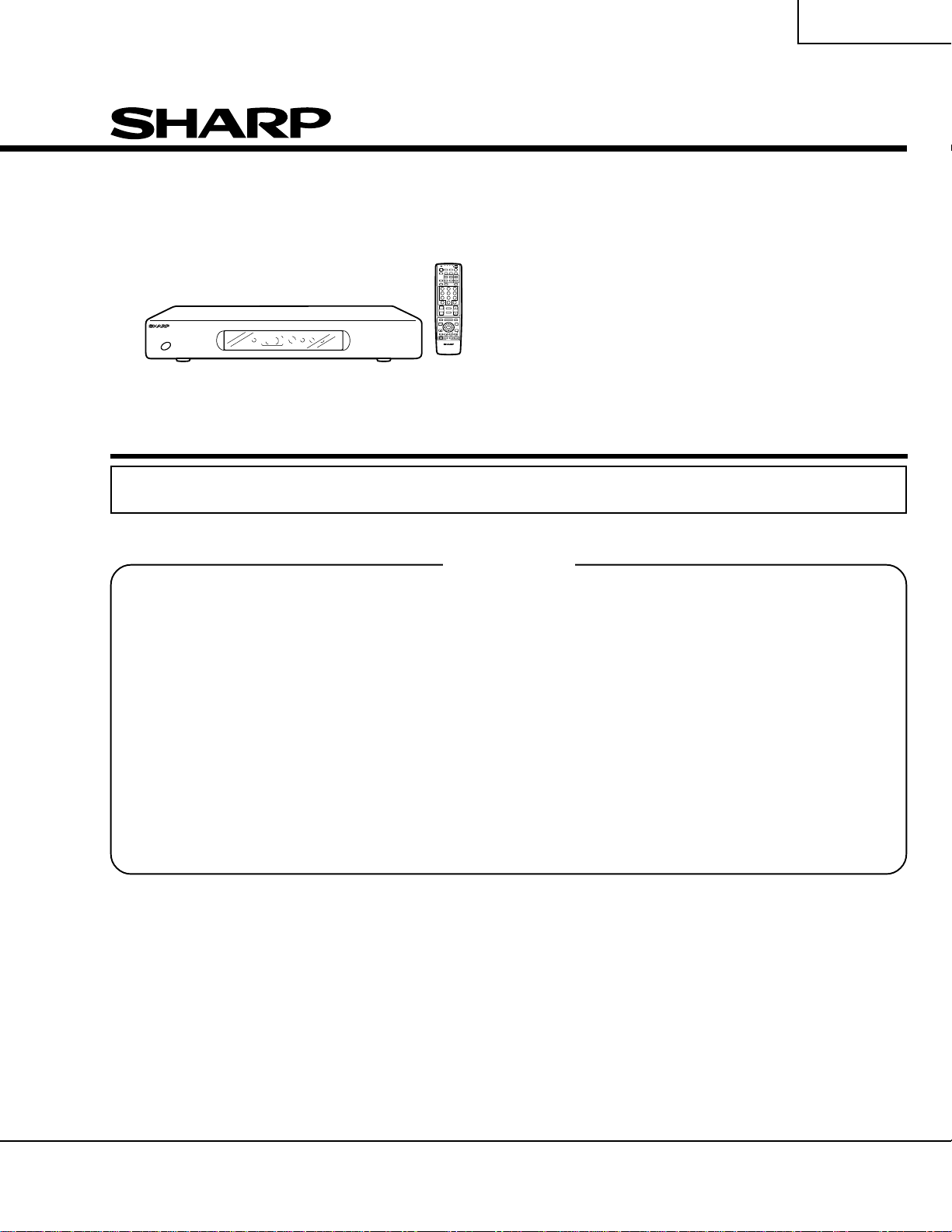
PZ-MR2T
PZ-43MR2U
PZ-50MR2U
SERVICE MANUAL
S12F4PZ50MR2U
PLASMA DISPLAY TV
(AVC SYSTEM)
PZ-MR2T
PZ-43MR2U
MODELS
In the interests of user-safety (Required by safety regulations in some countries) the set should be restored
to its original condition and only parts identical to those specified should be used.
PZ-50MR2U
CONTENTS
Page
» IMPORT ANT SER VICE SAFETY PRECAUTION .....2
» SPECIFICATIONS................................................4
» OPERA TION MANUAL ........................................5
» DIMENSIONS ....................................................13
» REMOVING OF MAJOR PARTS .......................14
» ADJUSTMENT PROCEDURES.........................16
» DESCRIPTION OF MAJOR IC FUNCTIONS ....22
» TROUBLE SHOOTING TABLE..........................49
» PRINTED WIRING BOARD BLOCK DIAGRAM .. 56
» SYSTEM BLOCK DIAGRAM ............................. 58
» SIGNAL FLOW BLOCK DIAGRAM....................60
» DC/DC CONVERTER BLOCK DIAGRAM .........62
» POWER BLOCK DIAGRAM...............................64
» PC I/F BLOCK DIAGRAM ..................................66
» OVERALL WIRING DIAGRAM...........................68
» DESCRIPTION OF SCHEMATIC DIAGRAM .....72
» WAVEFORMS ....................................................73
» SCHEMA TIC DIAGRAM.....................................74
» PRINTED WIRING BOARD ASSEMBLIES...... 114
» P ARTS LIST .....................................................121
» P ACKING OF THE SET ...................................145
Page
SHARP CORPORATION
This document has been published to be used for
after sales service only.
The contents are subject to change without notice.
Page 2
PZ-MR2T
2
2
PZ-43MR2U
PZ-50MR2U
IMPORTANT SERVICE SAFETY PRECAUTION
Ë
Service work should be perfomed only by qualified service technicians who are thoroughly familiar with all safety checks and the servicing guidelines which follow:
WARNING
1. For continued safety, no modification of any circuit
should be attempted.
2. Disconnect AC power before servicing.
CAUTION: FOR CONTINUED
PROTECTION AGAINST A RISK
OF FIRE REPLACE ONLY WITH
SAME TYPE FUSE. F701 (T2A,
A V
250V), F702 (T2A, 250V), F1702
(T4AL, 250V) FUSE.
BEFORE RETURNING THE RECEIVER
(Fire & Shock Hazard)
Before returning the receiver to the user, perform
the following safety checks:
1. Inspect all lead dress to make certain that leads are
not pinched, and check that hardware is not lodged
between the chassis and other metal parts in the
receiver.
2. Inspect all protective devices such as non-metallic
control knobs, insulation materials, cabinet backs,
adjustment and compartment covers or shields,
isolation resistor-capacitor networks, mechanical
insulators, etc.
3. To be sure that no shock hazard exists, check for
leakage current in the following manner.
» Plug the AC cord directly into a 110~240 volt AC outlet,
and connect the DC power cable into the receiver's
DC jack. (Do not use an isolation transformer for this
test).
» Using two clip leads, connect a 1.5k ohm, 10 watt
resistor paralleled by a 0.15µF capacitor in series
with all exposed metal cabinet parts and a known
earth ground, such as electrical conduit or electrical
ground connected to an earth ground.
» Use an AC voltmeter having with 5000 ohm per volt,
or higher, sensitivity or measure the AC voltage drop
across the resisor.
» Connect the resistor connection to all exposed metal
parts having a return to the chassis (antenna, metal
cabinet, screw heads, knobs and control shafts,
escutcheon, etc.) and measure the AC voltage drop
across the resistor.
All checks must be repeated with the AC cord plug
connection reversed. (If necessary, a nonpolarized
adaptor plug must be used only for the purpose of
completing these checks.)
Any reading of 35V peak (this corresponds to 0.7
milliamp. peak AC.) or more is excessive and
indicates a potential shock hazard which must be
corrected before returning the monitor to the owner.
DVM
AC SCALE
1.5k ohm
10W
0.15 µF
TEST PROBE
TO EXPOSED
METAL PARTS
CONNECT TO
KNOWN EARTH
GROUND
234567890123456789012345678901212345678901234567890123456789012123456789012345678901234567890121
SAFETY NOTICE
Many electrical and mechanical parts in Plasma Display
television have special safety-related characteristics.
These characteristics are often not evident from visual
inspection, nor can protection afforded by them be
necessarily increased by using replacement components
rated for higher voltage, wattage, etc.
Replacement parts which have these special safety
characteristics are identified in this manual; electrical
and shaded areas in the
Schematic Diagrams
For continued protection, replacement parts must be
identical to those used in the original circuit.
The use of a substitute replacement parts which do not
have the same safety characteristics as the factory
recommended replacement parts shown in this service
manual, may create shock, fire or other hazards.
components having such features are identified by “ å”
234567890123456789012345678901212345678901234567890123456789012123456789012345678901234567890121
2
Replacement Parts List
.
and
Page 3
PZ-MR2T
2
2
PZ-43MR2U
PZ-50MR2U
PRECAUTIONS A PRENDRE LORS DE LA REPARATION
Ë
Ne peut effectuer la réparation qu' un technicien spécialisé qui s'est parfaitement
accoutumé à toute vérification de sécurité et aux conseils suivants.
AVERTISSEMENT
1. N'entreprendre aucune modification de tout circuit.
C'est dangereux.
2. Débrancher le récepteur avant toute réparation.
PRECAUTION: POUR LA PROTECTION
CONTINUE CONTRE LES RISQUES
D'INCENDIE, REMPLACER LE FUSIBLE
P AR UN FUSIBLE DE MEME TYPE F701
A V
(T2A, 250V), F702 (T2A, 250V), F1702
(T4AL, 250V).
VERIFICA TIONS CONTRE L'INCEN-DIE ET
LE CHOC ELECTRIQUE
Avant de rendre le récepteur à l'utilisateur, effectuer
les vérifications suivantes.
1. Inspecter tous les faisceaux de câbles pour s'assurer
que les fils ne soient pas pincés ou qu'un outil ne soit
pas placé entre le châssis et les autres pièces
métalliques du récepteur.
2. Inspecter tous les dispositifs de protection comme les
boutons de commande non-métalliques, les isolants,
le dos du coffret, les couvercles ou blindages de réglage
et de compartiment, les réseaux de résistancecapacité, les isolateurs mécaniques, etc.
3. S'assurer qu'il n'y ait pas de danger d'électrocution en
vérifiant la fuite de courant, de la facon suivante:
• Brancher le cordon d'alimentation directem-ent à une
prise de courant de 110-240V. (Ne pas utiliser de
transformateur d'isolation pour cet essai).
• A l'aide de deux fils à pinces, brancher une résistance
de 1.5 kΩ 10 watts en parallèle avec un condensateur
de 0,15µF en série avec toutes les pièces métalliques
exposées du coffret et une terre connue comme une
conduite électrique ou une prise de terre branchée à
la terre.
• Utiliser un voltmètre CA d'une sensibilité d'au moins
5000Ω/V pour mesurer la chute de tension en travers
de la résistance.
• Toucher avec la sonde d'essai les pièces métalliques
exposées qui présentent une voie de retour au châssis
(antenne, coffret métallique, tête des vis, arbres de
commande et des boutons, écusson, etc.) et mesurer
la chute de tension CA en-travers de la résistance.
T outes les vérifications doivent être refaites après avoir
inversé la fiche du cordon d'alimentation. (Si nécessaire,
une prise d'adpatation non polarisée peut être utilisée
dans le but de terminer ces vérifications.)
Tous les courants mesurés ne doivent pas dépasser
0,5 mA.
Dans le cas contraire, il y a une possibilité de choc
électrique qui doit être supprimée avant de rendre le
récepteur au client.
DVM
DVM
ECHELLE CA
AC SCALE
1.5k ohm
10W
0.15 µF
0.15µF
TEST PROBE
SONDE D'ESSAI
AUX PIECES
METALLIQUES
EXPOSEES
BRANCHER A UNE
TERRE CONNUE
234567890123456789012345678901212345678901234567890123456789012123456789012345678901234567890121
AVIS POUR LA SECURITE
De nombreuses pièces, électriques et mécaniques, dans
les téléviseurs présentent des caractéristiques spéciales
relatives à la sécurité, qui ne sont souvent pas évidentes
à vue. Le degré de protection ne peut pas être
nécessairement augmentée en utilisant des pièces de
remplacement étalonnées pour haute tension,
puissance, etc.
Les pièces de remplacement qui présentent ces
caractéristiques sont identifiées dans ce manuel; les
pièces électriques qui présentent ces particularités sont
234567890123456789012345678901212345678901234567890123456789012123456789012345678901234567890121
identifiées par la marque " å " et hachurées dans la
liste des pièces de remplacement et les diagrammes
schématiques.
Pour assurer la protection, ces pièces doivent être
identiques à celles utilisées dans le circuit d'origine.
L'utilisation de pièces qui n'ont pas les mêmes
caractéristiques que les pièces recommandées par
l'usine, indiquées dans ce manuel, peut provoquer des
électrocutions, incendies, radiations X ou autres
accidents.
3
Page 4
PZ-MR2T
PZ-43MR2U
PZ-50MR2U
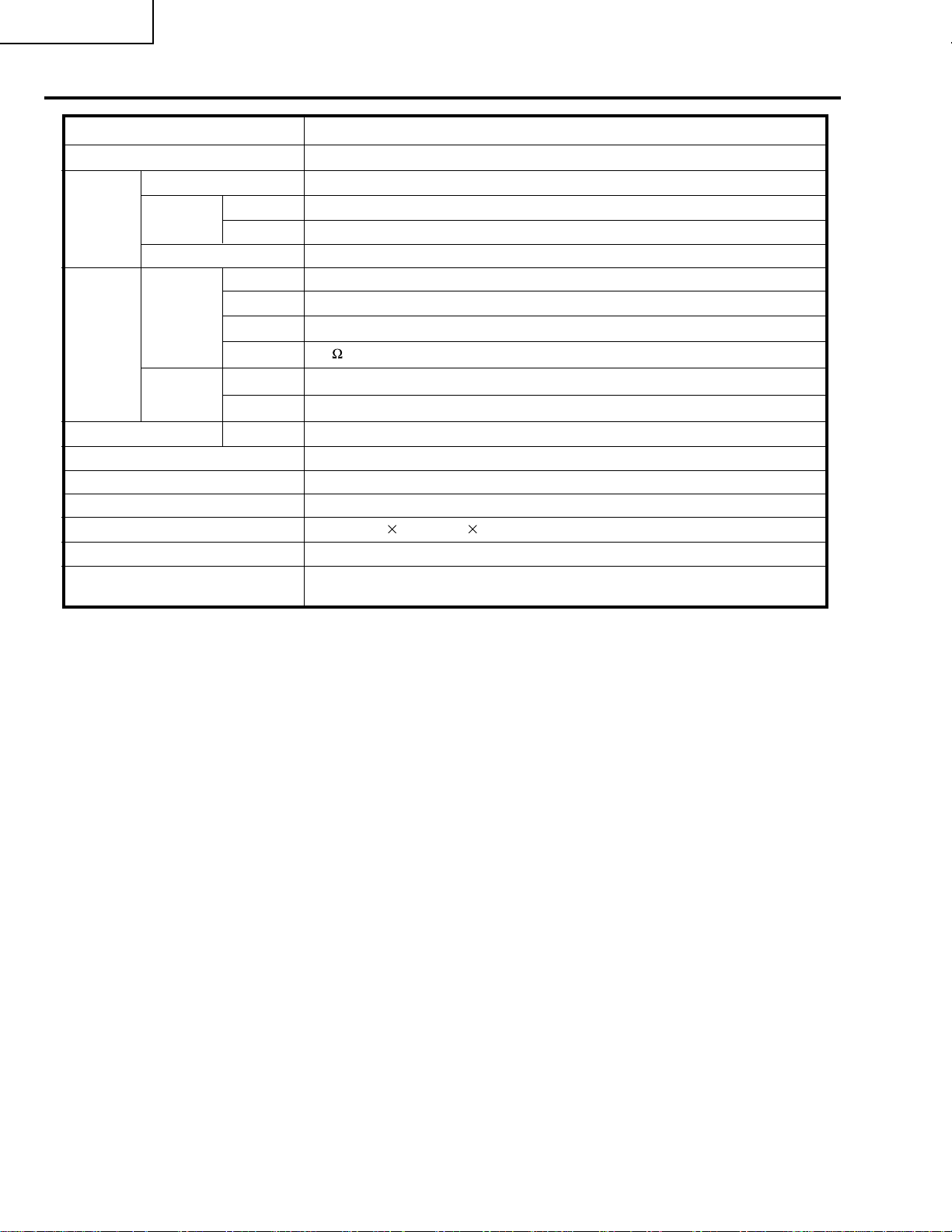
Specifications
Item AVC System, Model: PZ-50MR2U, PZ-43MR2U, PZ-MR2T
Color System
TV
Function
Terminals S-VIDEO in, AV in, COMPONENT in
Monitor Out Terminal
OSD Language English/French/Spanish
Other Features
Power Requirement
Dimensions
Weight
Accessories
Cercuit type
Tuner
Audio multiplex
Rear
Front
VHF/UHF
CATV
INPUT 1
INPUT 2 S-VIDEO in, AV in
INPUT 3
Antenna 75 UNBAL, F Type for VHF/UHF/CATV in
INPUT 4
PC INPUT
Rear
American TV standard NTSC system
PLL full synchronous detection, PLL digital synthesizer system
VHF 2–13ch, UHF 14–69ch
1–125ch
BTSC system
S-VIDEO in, AV in, COMPONENT in, RGB in
S-VIDEO, AV in
15 Pin mini D-Sub, Audio in
S-VIDEO out, AV out, Audio (Variable, Fixed)
Picture & Picture, Still image, Dual Tuner System
AC 110–240 V, 50/60 Hz, 40 W (0.6 W Standby)
16 15/16 (W) 2 25/32 (H) 13 (D) inch (430 (W), 70 (H), 330 (D) mm)
9.7 lbs(4.4 kg)
Power Cord, Remote control unit, Two AA size batteries, System Cable,
Operation manual
• Design and specifications are subject to change without notice.
4
Page 5
Operation Manual
AVC System
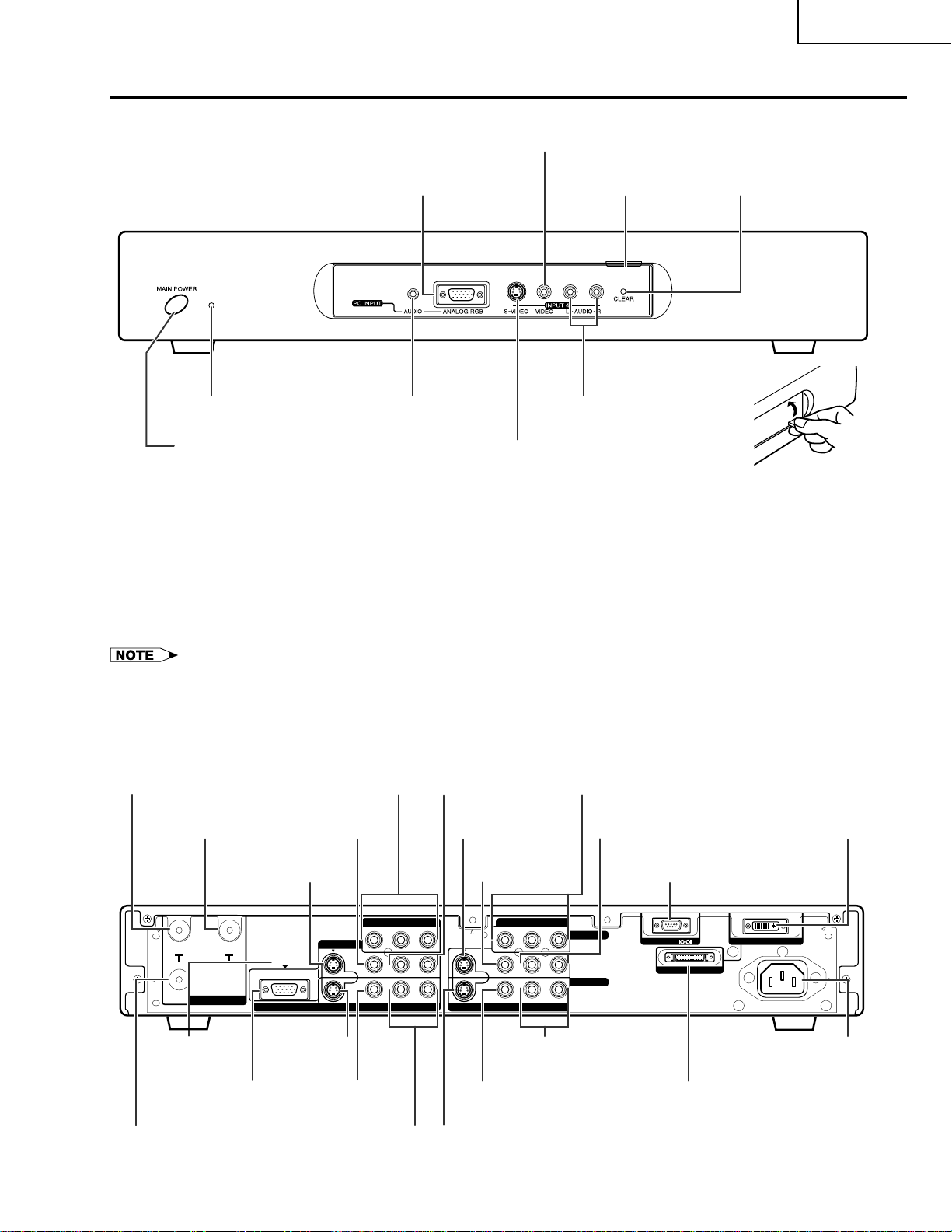
Front view
INPUT 4 terminal (VIDEO)
PZ-MR2T
PZ-43MR2U
PZ-50MR2U
STANDBY/ON indicator
POWER button
PC INPUT terminal (ANALOG RGB)
PC INPUT terminal (AUDIO)
INPUT 4 terminal (S-VIDEO)
Door knob
INPUT 4 terminals (AUDIO)
CLEAR button*
How to open the door.
* If you’re having problems operating the AVC System and want to return to normal screen, even when it stays
on (the indicator lights green), press CLEAR on the AVC System. Pressing CLEAR resets the System as
shown below.
• AV MODE resets to STANDARD
• TV channel returns to initial channel setting(Air:2ch, Cable:1 or 2ch)
• Twin picture resets to normal
• Audio setting initializes
• SRS resets to Off.
• Image position initializes
• Pressing CLEAR will not work if the System is in standby mode (indicator lights red).
• Pressing CLEAR will not delete channel preset or secret number
. See Page for initialising factory preset settings when
you know your secret number. See Page for initialising factory preset values when you have forgotten your secret
number.
Rear view
Antenna input
terminal (A)
Antenna input
terminal (B)
ANT-A ANT-B
ANT/CABLE 75OUT
USE FOR HDTV SIGNALS ONLY.
NOT INTENDED FOR USE WITH
COMPUTERS
Antenna output
terminal
INPUT 3 COMPONENT
video terminals
B, PR)
(Y, P
INPUT 3 terminal
(VIDEO)
INPUT 3 terminal
(S-VIDEO)
USE FOR HDTV SIGNALS ONLY.
NOT INTENDED FOR USE WITH
COMPUTERS
HD INPUT
MONITOR OUTPUT
INPUT 3
S-VIDEO
MONITOR OUTPUT
terminal (S-VIDEO)
HD
INPUT
terminal
MONITOR
OUTPUT
terminal (VIDEO)
MONITOR OUTPUT
terminals (AUDIO L/R)
COMPONENT
YP
BPR
VIDEO R-AUDIO-L
INPUT 3 terminals
(AUDIO L/R)
INPUT 1 terminal
(S-VIDEO)
INPUT 1 terminal
(VIDEO)
COMPONENT
YP
BPR
S-VIDEO VIDEO R-AUDIO-L
INPUT 2 terminals
(AUDIO L/R)
INPUT 2 terminal
(VIDEO)
INPUT 2 terminal
(S-VIDEO)
INPUT 1 COMPONENT
terminals (Y, P
B, PR)
INPUT 1 terminals
(AUDIO L/R)
after RS-232C terminal
INPUT 1
INPUT 2
RS-232C
DISPLAY OUTPUT-2
DISPLAY OUTPUT-2 terminal
DISPLAY OUTPUT-1
DISPLAY OUTPUT-1
AC INPUT
110V - 24OV
AC INPUT terminal
terminal
5
Page 6
PZ-MR2T
PZ-43MR2U
PZ-50MR2U
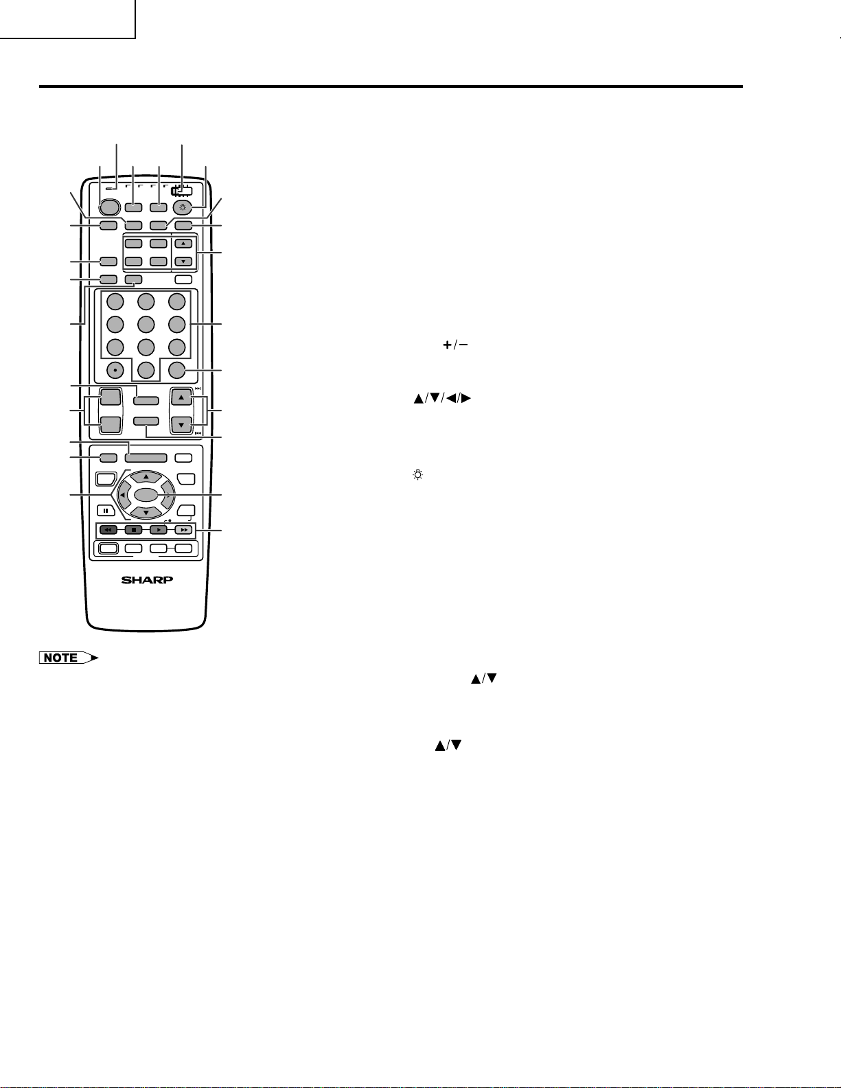
Remote control unit
24
12 13
1
2
3
4
5
TV
POWER
AV
MODE
VIEW
MODE
DISPLAY
123
6
456
789
7
8
9
10
+
VOL CH
–
MENU TV/SAT/DVD
RETURN
SOURCE DTV/SAT
POWER
11
ABCD
POWER
• When using the remote control unit, point it at the Plasma
Display TV(Panel Unit).
Mode switch
TV VCRCBL
DVD
/SAT
/LD
/DTV
ANT-A/B
INPUT
FRONT
SURROUND
MTS CC
TWIN
PICTURE
SELECT
SUB TWIN CH
FREEZE
INPUT
SLEEP LEARN
EDIT/
100
0
FLASHBACK
MUTE
DTV/DVD TOP
MENU
SET/
ENTER
VCR REC
FAVORITE CH
INPUT VOL– VOL+
RECEIVER
MENU
GUIDE
DTV/SAT
INFO
14
15
16
17
18
ENT
19
20
21
22
23
Set the mode switch to TV.
1TV POWER: Switch the Plasma Display TV power on or
off.
2 FRONT SURROUND: Set SRS and FOCUS Sound
System mode.
3 AV MODE:Select an audio or video setting.
4 VIEW MODE: Select the scr een size.
5 DISPLAY:Display the channel information.
6 SLEEP:Set the SLEEP timer.
7 FLASHBACK: Return to the previous channel or input
external mode.
8VOL
: Set the volume.
9 MENU:Display the menu screen.
10 MENU RETURN: Return to the previous menu screen.
11
12 ANT-A/B: Select the antenna. (A, B)
13 INPUT: Select an input sour ce of the Plasma Display
TV. (TV, INPUT 1, INPUT 2, INPUT 3, INPUT 4,
PC)
: When pressed all buttons on the remote control unit
14
will light. The lighting will turn off if no operations
are performed within about 5 seconds. This button
is used for performing operations in dark places.
15 MTS: Select the MTS/SAP.
16 CC: Display captions during closed-caption source.
17 TWIN CH buttons
TWIN PICTURE:Set the twin picture mode.
FREEZE: Set the still image. Press again to return to
normal screen.
SELECT: Select the active screen.
SUB INPUT: Select an input sour ce of sub screen.
TWIN CH
18 0 – 9: Set the channel.
19 100 ENT: Select the three digit mode. Execute a
command of the channel.
20 CH
: Select the channel.
21 MUTE: Mute the sound.
22 SET/ENTER: Execute a command.
23 FAVORITE CH
A, B, C, D: Select any of four preset channels. (See
page for details to set the FAVORITE CH.)
While watching you can toggle the set channels by
pressing A, B, C and D.
24 LED for transmission confirmation
(AV mode: ST ANDARD, DYNAMIC,
MOVIE, GAME, USER.
PC mode: ST ANDARD, USER.)
: Select a desired item on the setting screen.
Press again to return to normal
screen.
: Select the channel of sub screen.
6
Page 7
Preparation
Connecting the system
1.
Connecting the system cable, the power cor d and the speaker cables to the Plasma Displa y TV (Panel
Unit)
Plasma Display TV (Panel Unit) (rear view)
Black
Red
PZ-MR2T
PZ-43MR2U
PZ-50MR2U
Speaker cable
Speaker cable
(bottom view)
(WHITE)
(GRAY)
Red
Black
System cable
Speaker cables
(GRAY
GRAY with white stripe)
• Two speaker cables of different lengths are supplied. As
shown in the diagram, connect the longer speaker cable
to the left speaker and the shorter to the right.
2.
Connecting the system cable and the power cord to the AVC System
Power cord
As you apply pressure to this part,
insert the speaker cable. It is
important to match polarity when
connecting the speaker cables to the
terminals.
Insert the speaker cable
Lift up the snap clip.
Insert the wire into
the hole of the
connector.
Lower the snap clip
to grip the wire in
place.
System cable
(GRAY)
(WHITE)
AVC System (rear view)
COMPONENT
BPR
YP
HD INPUT
INPUT 3
S-VIDEO
VIDEO R-AUDIO-L
ANT-A ANT-B
ANT/CABLE 75OUT
MONITOR OUTPUT
• TO PREVENT RISK OF ELECTRIC SHOCK, DO NOT TOUCH UN-INSULATED PARTS OF ANY CABLES WITH THE
POWER CORD CONNECTED.
COMPONENT
YP
BPR
S-VIDEO VIDEO R-AUDIO-L
INPUT 1
INPUT 2
RS-232C
DISPLAY OUTPUT-2
DISPLAY OUTPUT-1
AC INPUT
110V - 24OV
Power cord
7
Page 8
PZ-MR2T
PZ-43MR2U
PZ-50MR2U
preparation
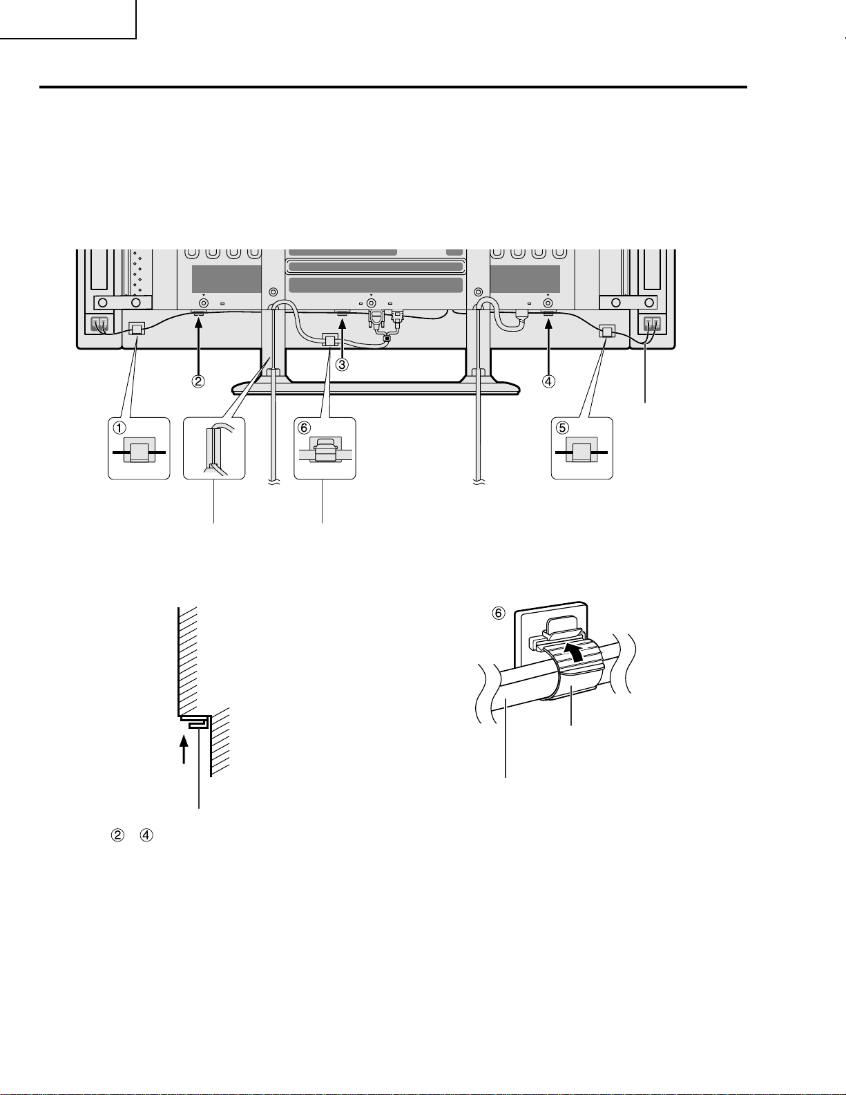
How to route cables
A system cable clamp and five speaker cable clamps are included with the system for cable management. Follow the
diagram below for correct cable management.
As viewed from the rear of the display.
Speaker cable
Speaker cable clamp
System cable
Wedge the power cord and the
system cable into the groove on the
stand.
Stick the speaker cable clamps
– ) to the surface as shown.
(
Power cord
Speaker cable clamp
System cable clamp
System cable clamp
System cable
8
Page 9
preparation
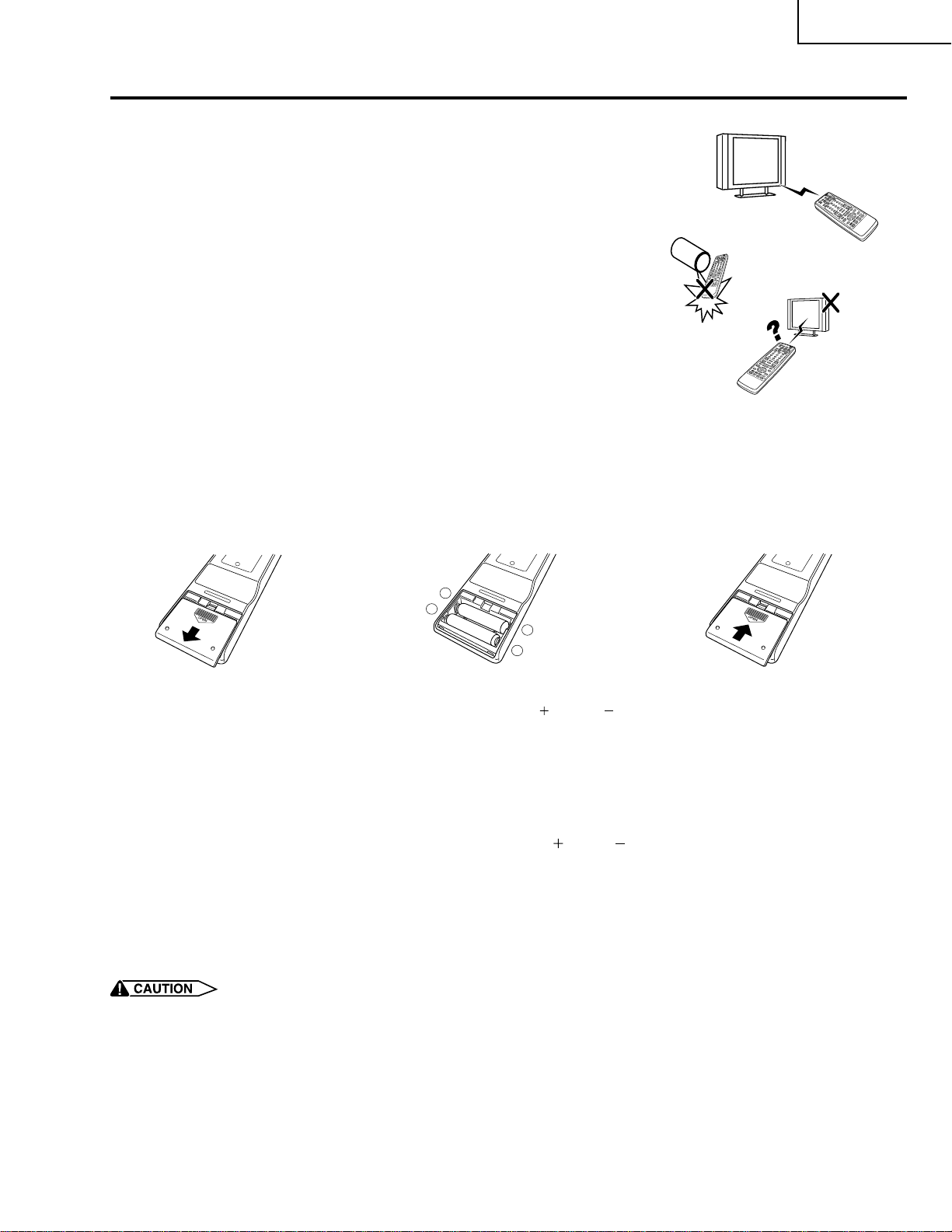
Using the remote control unit
Use the remote control unit by pointing it towards the remote sensor window.
Objects between the remote control unit and sensor window may pr event proper
operation.
Cautions regarding remote control unit
• Do not expose the remote control unit to shock. In addition, do not expose the
remote control unit to liquids, and do not place in an area with high humidity.
• Do not install or place the remote control unit under direct sunlight. The heat
may cause deformation of the unit.
• The remote control unit may not work properly if the remote sensor window of
the Plasma Display TV(Panel Unit) is under direct sunlight or strong lighting.
In such case, change the angle of the lighting or Plasma Display TV(Panel
Unit), or operate the remote control unit closer to the remote sensor window.
Inserting the batteries
If the remote control unit fails to operate Plasma Display TV functions, replace
the batteries in the remote control unit.
PZ-MR2T
PZ-43MR2U
PZ-50MR2U
1 Open the battery cover. 2 Insert batteries (two AA size
3 Close the battery cover.
batteries, supplied with product).
_
+
+
_
• Place batteries with their terminals
corresponding to the (
indicators in the battery compartment.
) and ( )
Cautions regarding batteries
Improper use of batteries can result in chemical leakage or explosion. Be sur e to follow the instructions below.
• Do not use manganese batteries. When you replace the batteries, use alkaline ones.
• Place the batteries with their terminals corresponding to the (
• Do not mix batteries of different types. Different types of batteries have different characteristics.
• Do not mix old and new batteries. Mixing old and new batteries can shorten the life of new batteries or cause
chemical leakage in old batteries.
• Remove batteries as soon as they have worn out. Chemicals that leak from batteries can cause a rash. If you
find any chemical leakage, wipe thoroughly with a cloth.
• The batteries supplied with this product may have a shorter life expectancy due to storage conditions.
• If you used the remote control unit for an extended period of time, remove the batteries from it.
) and ( ) indicators.
• WHEN DISPOSING OF USED BATTERIES, PLEASE COMPLY WITH GOVERNMENTAL REGULATIONS OR
ENVIRONMENTAL PROTECTION GUIDELINES THAT APPLY IN YOUR COUNTRY OR AREA.
9
Page 10

PZ-MR2T
PZ-43MR2U
PZ-50MR2U
Using external equipment
You can connect many types of external equipment to your Plasma Display TV, like a DVD player, VCR, Digital
tuner, computer, game console and camcorder. To view external source images, select the input source from
INPUT on the remote control unit or on the Plasma Display TV(Panel Unit).
Digital tuner
S-VIDEO
RGB
ANT-A ANT-B
AV Receiver
(Built-in T uner Amp)
DVD player
S-VIDEO
Y/P
INPUT 3
S-VIDEO
B/PR
COMPONENT
YP
VIDEO R-AUDIO-L
AV
BPR
COMPONENT
YP
BPR
S-VIDEO VIDEO R-AUDIO-L
S-VIDEO
Y/PB/P
INPUT 1
INPUT 2
R
AV
RS-232C
DISPLAY OUTPUT-2
AV
DISPLAY OUTPUT-1
AC INPUT
110V - 24OV
AVC System
(rear view)
AV
HD INPUT
ANT/CABLE 75OUT
MONITOR OUTPUT
S-VIDEO
VCR
AVC System
(front view)
PC-AUDIO
AV
Game console/
Computer
ANALOG RGB
S-VIDEO
• To protect all equipment, always turn off the AVC System before connecting to a DVD player, VCR, Digital tuner,
computer, game console, camcorder or other external equipment.
• Please refer to the relevant operation manual (DVD player, computer, etc.) carefully before making connections.
Camcorder
10
Page 11
PZ-MR2T
PZ-43MR2U
PZ-50MR2U
Appendix
RS-232C port specifications
Computer Control of the Plasma Display TV (Panel Unit)
• When a program is set, the display can be controlled from the computer using the RS-232C terminal.
The input signal (computer/video) can be selected, the volume can be adjusted and various other adjustments
and settings can be made, enabling automatic programmed playing.
•
Attach an RS-232C cable cross-type (commercially available) to the supplied Din-D/sub RS-232C for the
connections.
• This operation system should be used by a person who is accustomed to using computers.
Communication conditions
Set the RS-232C communications settings on the computer to match the display's communications conditions.
The display's communications settings are as follows:
Baud rate:
Data length:
Parity bit:
Stop bit:
Flow control:
9,600 bps
8 bits
None
1 bit
None
Communication procedure
Send the control commands from the computer via the RS-232C connector.
The display operates according to the received command and sends a response message to the computer.
Do not send multiple commands at the same time. Wait until the computer receives the OK response before
sending the next command.
Command format
Eight ASCII codes CR
C1 C2 C3 C4 P1 P2 P3 P4
Parameter
Input the parameter values, aligning left, and fill with blank(s) for the remainder. (Be sure that four values are input for the
parameter.)
When the input parameter is not within an adjustable range, “ERR” returns. (Refer to “Response code format”.)
No problem to input any numerical value for “x” on the table.
Command 4-digits:Command. The text of four characters.
Parameter 4-digits:Parameter 0 – 9, x, blank, ?
Return codeCommand 4-digits Parameter 4-digits
0
0009
–
30
100
0055
When “?” is input for some commands, the present setting value responds.
?
????
11
Page 12

PZ-MR2T
PZ-43MR2U
PZ-50MR2U
Appendix
Response code format
Normal response
OK
Return code (0DH)
Problem response (communication error or incorrect command)
ERR
Return code (0DH)
Command table
• About the command except being indicated here, it is outside the guarantee range of operation.
CONTROL ITEM COMMAND
POWER SETTING It shifts to standby.
INPUT SELECTION A TOGGLE
INPUT SELECTION B
AV MODE SELECTION
VOLUME
POSITION
WIDEMODE
SRS
TWIN PICTURE
CHANNEL
ANT-A/B
CC
TV
INPUT1-4
PC
INPUT 1
INPUT 3
H-POSITIONH-POSITION
V-POSITION
CLOCK
PHASE
DIRECT
CHANNEL
CH UP
CH DOWN
POWR
ITGD
ITVD
IAVD
IPCD
INP1
INP3
AVMD
VOLM
HPOS
VPOS
CLCK
PHSE
WIDE
SRSS
TWIN
DCCH
CHUP
CHDW
ANTS
CLCP
PARAMETER
_
_
_
0
_
_
_
x
_
_
_
0
_
_
_
*
_
_
_
x
_
_
_
0
_
_
_
1
_
_
_
2
_
_
_
0
_
_
_
1
_
_
_
2
_
_
_
3
_
_
_
0
_
_
_
1
_
_
_
2
_
_
_
3
_
_
_
4
_
_
_
5
_
_
*
*
_
*
*
*
_
*
*
*
_
*
*
*
_
*
*
*
_
*
*
*
_
*
*
*
_
_
_
0
_
_
_
1
_
_
_
2
_
_
_
3
_
_
_
4
_
_
_
5
_
_
_
6
_
_
_
7
_
_
_
8
_
_
_
0
_
_
_
1
_
_
_
2
_
_
_
3
_
_
_
4
_
_
_
0
_
_
_
1
_
*
*
*
_
_
_
x
_
_
_
x
_
_
_
x
_
_
_
0
_
_
_
1
_
_
_
2
_
_
_
3
_
_
_
4
_
_
_
5
(Toggle)
Input terminal number (1–4)
AUTO
AUTO
AV-Y/C
COMPONENT
AUTO
AV-Y/C
COMPONENT
RGB
(Toggle)
STANDARD
DYNAMIC
MOVIE
GAME
USER
Volume (0–60)
AV mode. (± 15)
PC mode. (± 90)
AV mode. (± 30)
PC mode. (± 60)
Only PC mode. (± 90)
Only PC mode. (± 20)
(Toggle) [AV]
Side Bar [AV]
S.Stretch [AV]
Zoom [AV]
Stretch [AV]
Normal [PC]
Full [PC]
Dot by Dot [PC]
Dot by Dot (W) [PC]
(Toggle)
(Toggle)
OFF
SRS
FOCUS
FOCUS
+
SRS
One screen
Twin screens
The channel number of TV
(1~125)
The channel number of TV 1
The channel number of TV 1
(Toggle)
(Toggle)
OFF
CC1
CC2
T1
T2
+
–
CONTROL CONTENTS
It input-switches by the toggle. (It is the same as an input change key)
It input-switches to TV. (A channel remains as it is. (Last memory))
It input-switches to INPUT1~INPUT4.
It input-switches to PC.
An input change is also included.
Although it can choose now, it is toggle operation in inside.
Although it can choose now, it is toggle operation in inside.
Toggle operation.
An input change is included if it is not TV display.
In Air, 2–69ch is effective.
In Cable, 1–125ch is effective.
If it is not TV display, it will input-switch to TV.
If it is not TV display, it will input-switch to TV.
Change toggle operation of tuner A/B.
Toggle operation of a closed caption.
• If an underbar (_) appears in the parameter column, enter a space.
• If an asterisk (*) appears, enter a value in the range indicated in brackets under CONTROL CONTENTS.
• As long as that from which the parameter (
) in the table is a numerical value, it may write anything.
12
Page 13
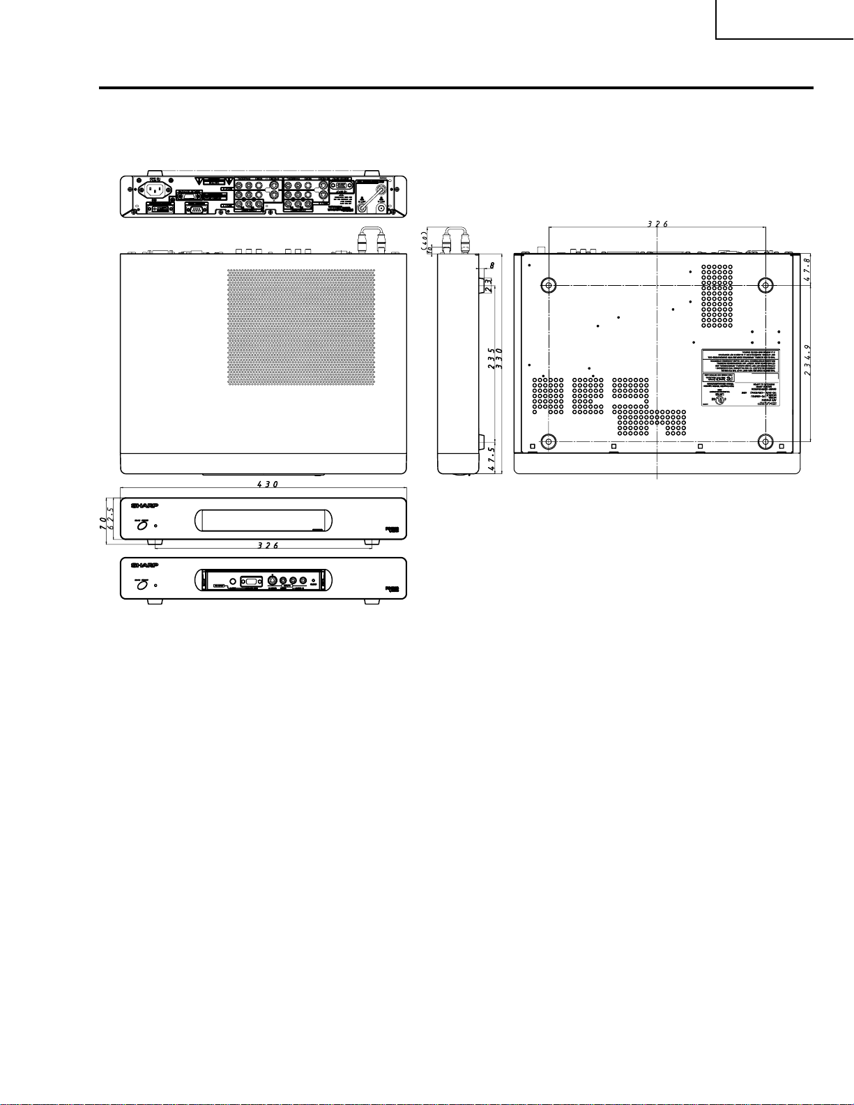
Dimensions
PZ-MR2T
PZ-43MR2U
PZ-50MR2U
(Unit: mm)
13
Page 14

PZ-MR2T
PZ-43MR2U
PZ-50MR2U
REMOVING OF MAJOR PARTS
1. Remove the six lock screws from the back of the top cabinet. Slide the top cabinet backward and detach it.
2. Remove the three lock screws from the front panel. Undo the three hooks at the top and the four hooks at the
bottom, and detach the front panel.
3. Remove the two hexagonal shafts from the front shield. Undo the four hooks on both sides and detach the
front shield.
4. Remove the three lock screws from the front unit and detach this unit.
5. Remove the one lock screw from the LED unit and detach this unit.
6. Remove the PC I/F unit and SR unit assemblies.
6-1. Remove the two hexagonal shafts each from the system cable (white) terminal and the RS-232C terminal,
both on the PC I/F unit.
6-2. Remove two lock screws from the system cable (gray) terminal also on the SR unit.
6-3. Remove the two lock screws from the PC I/F unit bracket.
6-4. Remove the four lock screws from the PC I/F unit and SR unit assemblies. Take out these assemblies.
6-5. Remove the three lock screws from the brackets of the PC I/F unit and SR unit assemblies. Detach the
shield.
6-6. Remove the six lock screws from the PC I/F unit. Detach this unit from the bracket.
6-7. Remove the two lock screws from the SR unit. Detach this unit from the bracket.
7. Remove the seven lock screws from the main unit and detach this unit.
6-4
PC I/F Unit
4
SR Unit
Front Unit
6-7
6-6
Power Unit
9-2
6-5
10
Main Unit
EMC Unit
Top cabinet
7
6-1
9-1
6-1
8-4
8-3
1
AV Unit
8-1
8-2
2
LED Unit
5
2
3
3
Bottom cabinet
14
Page 15

8. Remove the AV unit.
8-1. Remove the coaxial cable from the antenna terminal.
8-2. Remove the three lock screws from the antenna terminals
8-3. Remove the six lock screws from the AV unit.
8-4. Remove the six lock screws from the AV unit and detach this unit.
9. Remove the EMC unit assemblies.
9-1. Remove the two lock screws from the EMC unit bracket.
9-2. Remove the two lock screws from the EMC unit and detach this unit.
10. Remove the three lock screws from the power unit and detach this unit.
PZ-MR2T
PZ-43MR2U
PZ-50MR2U
15
Page 16

PZ-MR2T
PZ-43MR2U
PZ-50MR2U
ADJUSTMENT PROCEDURES
ËË
Ë Procedure for turning ON the power
ËË
1. Connecting the system
(1)Using the system cable, interconnect the plasma display and the AVC system.
(2)Connect the plasma display to the AC power source.
(3)Connect the AVC System to the AC power source.
2. Procedure for turning ON the power
(1)Turn ON the AC power switch located on the plasma display.
The power indicator on the plasma display will start blinking in red.
(When the AC power switch on the AVC System is not ON, the power indicator on the plasma display always
blinks in red.)
(2)Turn ON the power switch located on the AVC System.
The power indicator on the AVC System will be illuminated in green. Simultaneously , the power indicator on the
plasma display will change from blinking in red to illumination in green. Now the system has started up.
(3)If the power indicators on the AVC System and on the plasma display are both illuminated in red, press the
power key located on the remote controller and the power button located on the plasma display. The power
indicators on the plasma display and on the AVC System will change from red to green. Now the system has
started up.
ËË
Ë Procedure for upgrading the AVC System software
ËË
(1)With the power being OFF, open the top cabinet of the AVC System and then set the slide switch from the
NORMAL position to the WRITE position by inserting an insulated stick into the cutout located between the
WHITE port on the rear of the shield case for the PC I/F unit and the RS-232C port. (Or the software may be
upgraded by calling the process adjustment mode and using CENTER PROG UPDATE on the process
adjustment menu screen. This is discussed later.)
(2)Connect a program-installed PC to the AVC system using the RS-232C cross cable. (For the details of the
program, see Appendix.)
(3)Open the MS-DOS window on the PC and then go to the directory in which the software is installed.
(4)Start up the system to which the AVC System and plasma display have been connected.
(5)Run “vup.bat (tentative name)” at the MS-DOS prompt. The software will be upgraded.
(6)Load the file “civic_XXXXa.bhx main.bhx osd.bhx (tentative name)”.
It will take a couple of minutes until the file has been loaded. Never turn OFF the power or operate the system
during this rewriting period.
(7)After the file has been loaded, turn OFF the plasma display and the AVC System, and then return the slide
switch in the above step (1) back from the WRITE position to the NORMAL position. Now the software has been
upgraded.
ËË
Ë Procedure for adjusting each part of the AVC System
ËË
1. The adjustments were made to the best settings at factory. If any setting deviates or if any readjustment is
regarded as necessary when any part has been replaced, perform the following steps.
2. Any parameter that has been changed in the process adjustment mode is stored on the memory. If any
readjustment is required, write down the current value before changing it.
3. Use a stable AC power source.
4. If the program is upgraded, it will take approximately 1 minute for the EEPROM to be initialized before any
video appears. Therefore, you will need to wait for this time period. Do not turn OFF the power or operate the
system during the period.
5. If the program is rewritten, preferably write down the parameters that have been changed within the process
adjustment (see “OSD menu and parameters displayed at manual adjustment”), initialize the EEPROM, and
then reenter the recorded values.
16
Page 17

PZ-MR2T
PZ-43MR2U
PZ-50MR2U
ËË
Ë Entering a special mode
ËË
1. Entering the process adjustment mode
With the system being ON, turn OFF the main power of the plasma display. Next holding down the INPUT SELECT
and CH UP buttons on the plasma display itself, turn ON the main power again. Now the adjustment mode screen
shows up.
2. Adjustments in the adjustment process mode
[Steps]
Make adjustments using the process adjustment mode buttons, listed below.
[Description]
Following the items displayed on the process adjustment menu screen, adjust the settings given in their
adjustment tables.
3. Procedure for making factory settings
[Steps]
In the process adjustment mode, move the cursor to the line “INDUSTRY INIT” onscreen. T urn ON with the VOL
key and press the SET/ENTER key.
(Within the adjustment process, the channel settings remain unchanged. Once you exit the process adjustment
mode, the channel settings entered in the delivery adjustment mode become valid.)
[Description]
The user’s adjustment parameters and others will be set to the default values. Keep in mind that the channel
settings will also be initialized.
ËË
Ë Exiting the process adjustment mode
ËË
To exit the process adjustment mode, turn off the AVC System power.
ËË
Ë OSD menu and parameters displayed at manual adjustment
ËË
» The default values may slightly differ depending upon the program version to be rewritten.
» The settings are not initialized to the default values by merely rewriting the program. (See the paragraph for
Procedure for adjusting each part of the AVC System.)
(1)Descriptions of special buttons in process adjustment mode
(All on the remote controller)
Cursor UP key : Returns to the previous page.
Cursor DOWN key: Proceeds to the next page.
Vol UP key : Increases the adjusted value by 1.
V ol DOWN key : Decreases the adjusted value by 1.
Cursor RIGHT key : Increases the adjusted value by 10.
Cursor LEFT key : Decreases the adjusted value by 10.
CH UP key : Moves up the cursor.
CH DOWN key : Moves down the cursor .
(2)Process adjustment menu table
The items displayed on the menu screen must be written down before replacing the EEPROM at the AVC
System side.
ËË
Ë Procedure for replacing the PC I/F unit
ËË
Before replacing the PC I/F unit, write down the items displayed on each menu screen of the adjustment process.
If the I/F unit is completely broken and the above items cannot be jotted down in advance, follow the instructions
in “Adjustment procedures and items” and make all adjustments.
17
Page 18

PZ-MR2T
PZ-43MR2U
PZ-50MR2U
(2)Organization of process adjustment screen
Page Input Source Distinguish Signal HDCP
1/16 INPUT1 No SIG HDCP:ON
Ë
+Badj3.3V
Ë
+Badj2.5V
KEY WRITE
INDUSTRY INIT
CENTER Version
OSD version
CVIC Version
MONITOR version
PANEL Version
FLASH version
MONITOR Model
MODEL select MAIN
MODEL select AV
Model Select MONITOR
ST ANDBY TYPE
The example of a display
128
024
OFF
OFF
MR MAIN E 2001/11/14A
MR OSD 2001/09/06A
W2001/10/02 17.28 X2001/10/02 V2001/09/12 09.12
F6 91xx
-00
-01
11
2
1
Parameter display
Ë
+B Adj3.3V
Ë
+B Adj2.5V
Ë
SUB N358 Y
Ë
SUB N358 COLOR GAIN
Ë
SUB N358 TINT
Ë
N358 Y CONTRAST
Ë
N358 COLOR GAIN
Ë
MAIN CR GAIN N358
Ë
N358 TINT
Ë
MAIN CONTRAST 15K
Ë
MAIN SUB BRIGHT 15K
Ë
COMP 15K Y CONTRAST
Ë
COMP 15K COLOR GAIN
Ë
MAIN CR GAIN COMP 15K
Ë
COMP HDTV CONTRAST
Ë
COMP HDTV SUB BRIGHT
Ë
PEAK ACL SW
Setting range
0 ~ 255
0 ~ 255
0~ 63
0~ 63
0~ 63
0~ 63
0~ 63
0 ~ 255
0~ 63
0~ 63
0~ 15
0~ 63
0~ 63
0 ~ 255
0~ 63
0~ 63
OFF/ON
Description
3.3 V adjustment
2.2 V adjustment
Sub N358 Y level adiustment
Sub N358 color gain adjustment
Sub N358 tint adjustment
Main N358 Y contrast adjustment
Main N358 color gain adjustment
Main N358 Cr level adjustment
Main N358 Tint adjustment
Main Contrast adjustment (15k)
Main sub bright adjustment (15k)
COMP 15k Y level adjustment
COMP 15k Color gain adjustment
COMP 15k Cr level adjustment
COMP HDTV contrast level adjustment
COMP HDTV black level adjustment
The values for the above parameters should be written down before the EEPROM is replaced on
the A VC System.
18
Page 19

PZ-MR2T
PZ-43MR2U
PZ-50MR2U
ËË
Ë Procedures before and after replacing the PC I/F unit
ËË
1) Before replacing the PC I/F unit, write down the values for the parameters listed on the 2nd and 3rd pages of
the Adjustment Process A screen.
If the values for the parameters cannot be written down because the PC I/F unit is completely broken or for any
other reason, make all the adjustments in accordance with the paragraph for Adjustment procedure and
parameters, rather than the following procedures. (End)
Set the parameters listed on the 2nd and 3rd pages of the Adjustment Process A screen to the values you have
written down.
ËË
Ë Adjustment parameters
ËË
1) Analog adjustment
(1) Prior adjustment for AVC system chassis
Adjustment item Description Adjustment procedure
1 Process adjustment
mode
Call the process adjustment mode.
2 AVC center 3.3V
adjustment
3 AVC center 2.5V
adjustment
(2)
N358 signal adjustment
Adjustment item Description Adjustment procedure
1 Setup
2 Tuner level adjustment
3 MAIN N358 Y
CONTRAST
adjustment
Connect DC voltmeter to
TP1702.
Connect DC voltmeter to
TP1701.
» MAIN side
» SUB side
Adjust output voltage of DC/DC 3.3 V line to
3.25 ±0.01 V.
Adjust output voltage of DC/DC 2.5 V line to
2.6 ±0.01 V.
1. Receive the SPLIT FIELD color bar signal.
white 100%, 75% color bar, modulation
1. Adjust the V-LEVEL (R1 121) control so that the tuner output
(TP1101) on the AV PWB (DUNTKA616) should be
1.0 ±0.02 Vp-p.
2. Adjust the V -LEVEL (R1219) control so that the tuner output
(TP1201) on the AV PWB (DUNTKA616) should be
1.0 ±0.02 Vp-p.
1.0Vp-p
1. Adjust TB1274_MAIN output (pin (1) of P801)
to 0.7 ±0.01 Vp-p.
0.7Vp-p
4 MAIN N358 COLOR
GAIN adjustment
5 MAIN N358 TINT
adjustment
1. Adjust TB1274_MAIN output (pin (3) of P801) so that the
level shown below should be 0.3 ±0.01 Vp-p.
0.3Vp-p
1. Adjust TB1274_MAIN output (pin (3) of P801) so that the
waveform should become as shown below.
Smoothed
19
Page 20
PZ-MR2T
0.3Vp-p
0.9Vp-p
0.68Vp-p
0.7Vp-p
0.7Vp-p
PZ-43MR2U
PZ-50MR2U
Adjustment item Description Adjustment procedure
6 MAIN N358 Cr level
adjustment
1. Adjust TB1274_MAIN output (pin (5) of P801) so that the
level shown below should be 0.3 ±0.01 Vp-p.
7 MAIN N358
CONTRAST
Peak ACL: OFF
Check DC Tran 01
adjustment
Press the TWIN PICTURE
key.
8 SUB N358 Y LEVEL
adjustment
9 SUB N358 COLOR
GAIN adjustment
(3) Component 15 kHz signal adjustment
Adjustment item Description Adjustment procedure
1 Setup
1. T urn of f the PEAK ACL control. Adjust the output (TP815) of
IC810 to have 1.1 Vp-p from the pedestal level.
Adjusted value: 1.1 ±0.02 V
1. Select the special TWIN PICTURE settings for adjustment
(so that the same video source is reflected on MAIN/SUB).
1. Adjust TB1274_SUB output (TP806) to 0.9 ±0.02 Vp-p.
1. Adjust TB1274_SUB output (TP805) so that the level shown
below should be 0.68 ±0.01 Vp-p.
1. Select the component 15 kHz source (100% white color bar
signal).
2 COMPONENT
15 kHz Y level adjustment
3 COMPONENT
15 kHz COLOR GAIN
adjustment
4 COMPONENT
15 kHz Cr level
adjustment
1. Adjust TB1274_MAIN output (pin (1) of P801)
to 0.7 ±0.01 Vp-p.
1. Adjust TB1274_MAIN output (pin (3) of P801) so that the
level shown below should be 0.7 ±0.01 Vp-p.
1. Adjust TB1274_MAIN output (pin (5) of P801) so that the
level shown below should be 0.7 ±0.01 Vp-p.
20
Page 21
(4) Component HDTV signal adjustment
Adjustment item Description Adjustment procedure
1 Setup
PZ-MR2T
PZ-43MR2U
PZ-50MR2U
1. Select the component HDTV source (100% white color bar
signal).
2 COMPONENT
HDTV CONTRAST
Peak ACL: OFF
1. T urn of f the PEAK ACL control. Adjust the output (TP815) of
IC810 to have 1.1 ±0.02 Vp-p from the pedestal level.
adjustment
2. Factory settings
Adjustment item Description Adjustment procedure
1 INDUSTRY INIT
Then turn off the AC power supply of the AVC System. (Be careful not to use the power switches of the remote controller and
panel unit.)
IC1401
AV SWITCH
IC1102
P1301
CONNECTOR
Check the PEAK ACL is "ON" and DC Tran is "00".
Press the Delivery Setup key on the remote controller. Or position
the cursor on the INDUSTRY INIT line, set the line to ON with
the VOL key, and then press the ENTER key. The adjustment is
finished when the line turns OFF.
IC1301
AV SWITCH
SC1102J1104SC1101J1103
IC1602
CCD
IC1601
V-CHIP
SC1103
TP1101
TU1102 U/V TUNER
TU1101 U/V TUNER
SC1502
CONNECTOR
TP806
TP805
SC1501
CONNECTOR
P1901
PROGRAMMING
CONNECTOR
TP815
P1502
CONNECTOR
IC802
SUB VIDEO CHROMA
IC1901
PLD
IC403
CONTROL
IC803
RGB DECODER
IC7002
MEMORY
SC1401
CONNECTOR
IC402
SUB COMB FILTER
IC604
SYNC SEPARATE
P801
IC801
MAIN VIDEO CHROMA
SC1503
CONNECTOR
SC1504
CONNECTOR
IC7001
Y/C SEPERATE
L1718
L1708
L1710
P2503
CONNECTOR
TP1701
IC1502
DAC
IC1603
V-CHIP
SC1402
CONNECTOR
TP1201
P2502
CONNECTOR
P1703
CONNECTOR
T1701
R1219
P2501
CONNECTOR
P1702
CONNECTOR
L1711
R1121
IC2501
MULTI SOUND
TP1702
IC1502
DAC
21
Page 22

PZ-MR2T
PZ-43MR2U
PZ-50MR2U
DESCRIPTION OF MAJOR IC FUNCTIONS
Æ Description of Main ICs
»»
» IC1301 (CXA2069Q)
»»
This IC is a 7-input, 3-output selector.
The video signals other than those for the PC and components, which have been input from each input connector
and the tuner, and all the audio signals are sent to the IC1301 and then selected.
The video signals sent to the IC1301 are then input to the YC separation circuits, IC7001 (main) and IC402 (sub).
The audio signals are input to the PC I/F Unit via IC2501 (sound processor).
»»
» IC1401 (MM1519XQ)
»»
This IC is a 4-input, 3-output video selector for component input.
The VIDEO-1/3 Y/Pb/Pr signals, RGB component input and TV signal are input to the IC1401. The output signals
go to the main, sub, and component channels.
»»
» IC2501 (IX3370CE)
»»
This IC is used to decode audio signals.
It serves as both the S-IF decoder and the selector for the input audio data.
»»
» IC801/IC802 (TB1274AF)
»»
This IC is intended for color TV brightness, chroma demodulation and sync processing.
It receives the main and sub brightness signals and color signals from IC7001 (main) and IC402 (sub) in the
preceding stage, and gives out color difference signals.
»»
» IC803 (CXA2101Q)
»»
With a high-performance picture correction circuit incorporated, this IC consists of a base band video signal
processing section for color difference input and a video switch (including HV sync signal processing).
Input selection is performed by INPUT-SEL (IIC BUS). The Y/Pb/Pr signals of Y/Cb/Cr/HD and their respective HV
sync signals are input to each line.
As the multi-scanning compliance range, a horizontal scanning frequency of 15-60 kHz can be input.
»»
» IC1901 (IXA194WJ)
»»
This IC is FPGA for the synchronizing system.
It creates sand castle pulses for IC803 and generates horizontal blanking signals.
»»
» IC604 (TA1318AF)
»»
This IC synchronizes TV component signals.
The IC604 incorporates the necessary functions for measuring the frequency of input signals and synchronous
replay into a single chip, and is applicable for horizontal synchronous replay (15.75, 31.5, 33.75, and 45 kHz) and
vertical synchronous replay (525I, 525P, 625I, 750P, 1125I, 1125P, PAL 100 Hz, and NTSC 120 Hz).
»»
» IC7001 (PD64082)
»»
Through 3-dimensional NTSC signal processing, the PD64082 performs high-precision Y/C separation for main
video signals sent from the IC1301.
In combination with a 4Mbit EDO (Hyper Page Mode) DRAM, this IC forms 3-dimensional Y/C separation and
YNR/CNR system.
»»
» IC402 (CXD2093Q)
»»
This IC is a comb filter in the applicable field. Being a single high-precision Y/C chip, the 3-line comb filter performs
the Y/C separation of the sub channel video signals that have been output from IC1301.
»»
» IC804/IC810 (IX3473CE)
»»
The IC804 is a 6.7 MHz low-pass filter, incorporating a 6 dB amplifier, for the sub screen.
The IC810, on the other hand, is a 6.7 MHz low-pass filter, also incorporating a 6 dB amplifier, for the main screen
(for SDTV).
»»
» IC811 (IX3474CE)
»»
This IC is a 30 MHz low-pass filter, incorporating a 6 dB amplifier, for the main screen (for HDTV).
22
Page 23

PZ-MR2T
PZ-43MR2U
PZ-50MR2U
»»
» IC1701 (FA3675CE)
»»
This IC is designed to control the 6-channel PWM switching regulator.
With 5 step-up switching regulator lines incorporated, the IC converts +10V to +2.5V, +3.3V and +5.8V.
Also with a step-down switching regulator line incorporated, the IC converts +10V to +6.0V , -5.0V, +12V and +35V.
The lines are individually turned on and off.
»»
» IC1602 (Z86129S)
»»
The Z86129S is built in the TV decoder circuit and serves to process the vertical blanking interval (VBI) data that
has come from the video signal field of the data corresponding to the transmission format defined by EIA-608.
The data flowing along Line 21 is composed of the data of some multiplexed data channels.
Field 1 has 4 data channels: 2 caption channels and 2 text channels.
Field 2 has 5 additional data channels: 2 caption channels, 2 text channels and expansion data service (XDS)
channel. On any of these 9 data channels, the data transmitted can be recovered and displayed.
»»
» IC1601/IC1603 (Z86230S)
»»
The Z86230S functions for the process expansion data service (XDS) in Field 2 during the vertical blanking
interval (VBI).
The XDS data is processed in order to specify the Program Blocking (PB) signal or recovered XDS data packets.
The on-chip XDS filter in the Z86230S enables to recover the XDS data packets only for programming.
The Z86230S is compatible with monitors (Picture-In-Picture) for violence blocking and other XDS data service.
23
Page 24

PZ-MR2T
PZ-43MR2U
PZ-50MR2U
Æ Description of Functions of Main ICs on PC I/F Unit
»»
» IC4 (CXA3506R)
»»
This IC is an A/D converter that incorporates a 3-channel, 8-bit, 120 MSPS amplifier and PLL. It is used for the
video signals input to the I/F board on the main channel in the 1-screen and 2-screen modes, and also for the
video signals input from the front for the PC.
The video signals (analog RGB) from the CN6 are input to IN1 of IC4.
For the PC, the video signals (analog RGB) from CN8 are input to IN2 of IC4.
The input video signals are converted into digital signals and then sent to IC25.
»»
» IC310 (TLC5733A)
»»
This IC is a 3-channel, 8-bit, 20 MSPS A/D converter.
It is used for the sub-channel of the video signals input to the PC I/F Unit in the 2-screen mode.
The video signals (analog Y, Cb, Cr) from CN6 are input to IC310.
The video signals input to this IC are converted into digital signals and then sent to IC25.
»»
» IC25 (IX3434CE)
»»
This IC performs the I/P conversion and scaling to match the digitalized video with the output resolution, and also
the data conversion.
It has two input lines, V0 and V1. The V0 line is used to process the RGB, composite, and skirt signals input to the
480i and 580i components for the sub-channel in the 2-screen mode. The V1 line is used to process all the signals
as well as V1 for the main channel in the 1-screen and 2-screen modes.
The IC25 detects what resolution is input from the input synchronizing signal; creates H synchronization in
accordance with the frequency division ratio; creates the clamp signal in accordance with the input synchronizing
signal; and performs the data matrix conversion.
The video signals input to this IC is sent to IC413.
»»
» IC413 (SiL168)
»»
This IC is a panel link transmitter.
It converts the 8-bit RGB video data output from IC25 into the differential TMDS signals and then digitally transmits
the converted signals to the monitor.
The TMDS signals are transmitted at the frequency 10 times higher than the clock frequency.
»»
» IC1 (IX3270CE)
»»
This IC is a 1-chip RISC microprocessor.
It performs communication with the monitor and operates the system.
The IC1 also controls each IC in the AVC System and partially manages the power source.
»»
» IC405 (uPD4721)
»»
This IC is an RS-232 line driver receiver conforming to the EIA/TIA-232-E standard.
The IC405, when connected to a PC, allows for externally controlling the system.
It is also applicable for upgrading IC1.
24
Page 25

PZ-MR2T
PZ-43MR2U
PZ-50MR2U
» The information shown in the list is basic information and may not correspond exactly to that shown in the schematic diagrams.
Ë VHiCXA2069Q-1 (ASSY: IC1301)
» S2-Compatible, 7-Input/3-Ouput AV Switch
» Block Diagram
25
Page 26
PZ-MR2T
PZ-43MR2U
PZ-50MR2U
» Pin Function
Pin No. Pin Name I/O Pin Function
63
1
8
15
22
30
60
3
10
17
24
49
5
12
19
26
51
62, 2
9, 16
23, 29
59, 64
4, 11
18, 25
31, 61
53
41
44
56
39
58
47
37
52
43
38
54
45
40
6
13
20
27
7
14
21
28
32
33
34
36
55
46
48
50
TV
V1
V2
V3
V4
V5
V6
Y1
Y2
Y3
Y4
YIN1
C1
C2
C3
C4
CIN1
LTV, LV1
L V2, LV3
L V4, LV5
L V6, RTV
RV1, RV2
RV3, RV4
RV5, RV6
VOUT1
VOUT3
V/YOUT2
YOUT1
YOUT3
COUT1
COUT2
COUT3
LOUT1
LOUT2
LOUT3
ROUT1
ROUT2
ROUT3
S2-1
S2-2
S2-3
S2-4
S-1
S-2
S-3
S-4
ADR
SCL
SDA
DC OUT
TRAP1
TRAP2
MUTE
BIAS
I
I
I
I
I
I
I
I
I
I
I
I
I
I
I
I
I
I
I
I
I
I
I
I
O
O
O
O
O
O
O
O
O
O
O
O
O
O
I
I
I
I
I
I
I
I
I
I
I
O
I
I
I
I
Video signal input.
Composite video signal input
Y/C-separated signal input terminal for luminance signal input.
YIN1 to feed in the Y/C-separated signal of VOUT1 output.
Y/C-separated signal input terminal for chrominance signal input.
CIN1 to feed in the Y/C-separated signal of VOUT1 output.
Audio signal input terminal.
Video signal output terminal for composite video signal output.
Video signal output terminal for selection between composite video signal output and
luminance signal output by I2C Bus control.
Video signal output terminal for luminance signal output.
Video signal output terminal for chrominance signal output.
Audio signal output terminal.
Used to detect C signal-superimposed, S2-compatible DC level. 4:3 video signal when
below 1.3V. 4:3 letterbox signal when between 1.3V and 2.5V. 16:9 image squeeze
signal when above 2.5V. To be pulled down to GDN at 100KΩ to produce 4:3 video
signal when open.
Used to switch between composite video and S signals. Detection results to be written
in status register. S signal when below 3.5V. Composite video signal when above 3.5V .
To be pulled up to 5V at 100KΩ to produce composite video signal when open.
Used to select I2C Bus slave address. 90H when below 1.5V. 92H when above 2.5V.
90H also when the terminal is open.
I2C Bus signal input terminal.
I2C Bus signal input terminal.
Used to feed out S2-compatible DC level to be superimposed on COUT3 output. DC to
be superimposed by connecting to COUT3 output via a capacitor. Control to be made
by I2C Bus. S2-specified output impedance of 10 ±3KΩ to be realized by adding an
external resistance of 4.7KΩ.
Subcarrier trap circuit to be connected.
Audio signal output mute terminal. Mute off when below 1.3V. Mute on when above
2.5V. Mute off when the terminal is open.
Internal reference bias (Vcc/2) terminal. To be connected to GND with a capacitor in
between.
26
Page 27
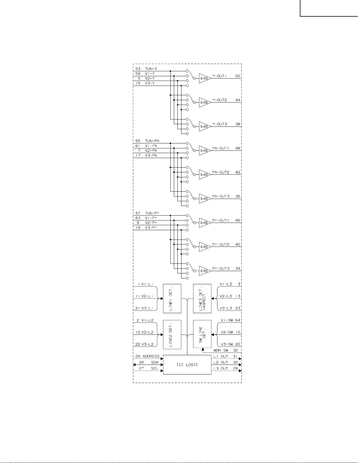
Ë VHiMM1519XQ-1(IC1401)
» Component Input Video Switch
» Block Diagram
PZ-MR2T
PZ-43MR2U
PZ-50MR2U
27
Page 28

PZ-MR2T
PZ-43MR2U
PZ-50MR2U
» Pin Function
Pin No. Pin Name I/O Pin Function
1
2
3
11
12
13
21
22
23
4, 14, 39, 45, 52,
58
51
5
15
53
59
24
6, 8, 16, 18, 33,
35, 37, 41, 43, 47,
49, 54, 56, 60, 62
7
9
17
19
55
57
61
63
10
20
32
64
25
26
27
28
29
30
31
34
36
38
40
42
44
46
48
50
VIDEO 1-L1
VIDEO 1-L2
VIDEO 1-L3
VIDEO 2-L1
VIDEO 2-L2
VIDEO 2-L3
VIDEO 3-L1
VIDEO 3-L2
VIDEO 3-L3
VCC
AVCC
VIDEO 2-Y
VIDEO 3-Y
TUNER-Y
VIDEO 1-Y
DGND
GND
VIDEO 2-Pb
VIDEO 2-Pr
VIDEO 3-Pb
VIDEO 3-Pr
TUNER-Pb
TUNER-Pr
VIDEO 1-Pb
VIDEO 1-Pr
VIDEO 2-SW
VIDEO 3-SW
MONO-SW
VIDEO 1-SW
ADDRESS
SDA
SCL
DVCC
L3 OUT
L2 OUT
L1 OUT
Pr OUT 3
Pb OUT 3
Y OUT 3
Pr OUT 2
Pb OUT 2
Y OUT 2
Pr OUT 1
Pb OUT 1
Y OUT 1
—
—
—
—
I/O
—
O
O
O
O
O
O
O
O
O
O
O
O
I
I
I
I
I
I
I
I
I
I
I
I
I
I
I
I
I
I
I
I
I
I
I
I
I
I
I
Line input of D-terminal
Analog power supply (9V)
Y -signal input
GND
Pb, Pr signal input
Switch line of D-terminal
Slave address select pin
Data input of I2C bus
Clock input of I2C bus
Digital power supply (5V)
Line output for monitor
Video signal output
28
Page 29
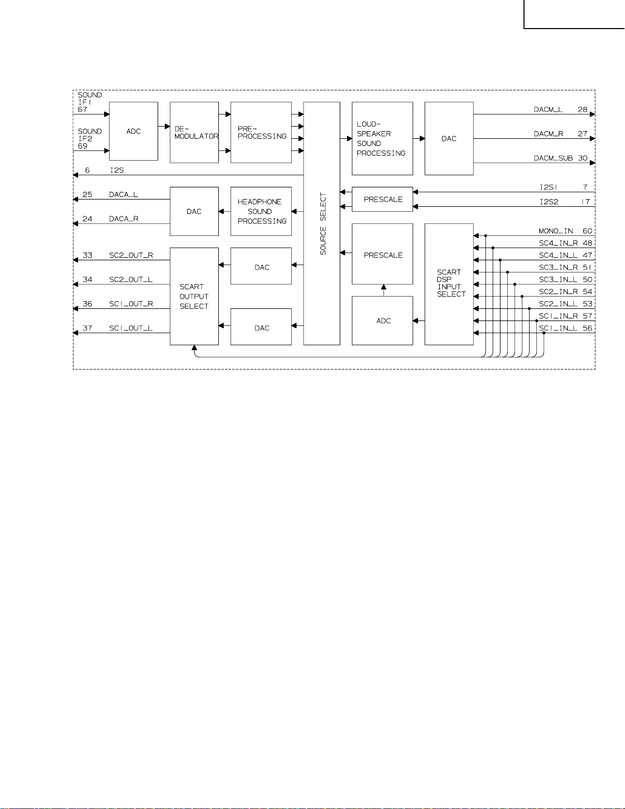
Ë RH-iX3370CEN1 (ASSY: IC2501)
» Multi Standard Sound Processor
» Block Diagram
PZ-MR2T
PZ-43MR2U
PZ-50MR2U
29
Page 30
PZ-MR2T
PZ-43MR2U
PZ-50MR2U
» Pin Function
Pin No. Pin Name I/O Pin Function
1
2
3
4
5
6
7
8
9
10
11, 12, 13
14, 15, 16
17
18, 19, 20
21
22, 23
24
25
26
27
28
29
30
31, 32
33
34
35
36
37
38
39
40
41, 42
43, 44
45
46
47
48
49
50
51
52
53
54
55
56
57
58
59
60
61, 62
63, 64
65, 66
67
68
69
70
71
72
73
74
75, 76
77
78
79
80
NC
I2C_CL
I2C_DA
I2S_CL
I2S_WS
I2S_DA_OUT
I2S_DA_IN1
ADR_DA
ADR_WS
ADR_CL
DVSUP
DVSS
I2S_DA_IN2
NC
RESETQ
NC
DACA_R
DACA_L
VREF2
DACM_R
DACM_L
NC
DACM_SUB
NC
SC2_OUT_R
SC2_OUT_L
VREF1
SC1_OUT_R
SC1_OUT_L
CAPL_A
AHVSUP
CAPL_M
NC
AHVSS
AGNDC
NC
SC4_IN_L
SC4_IN_R
ASG4
SC3_IN_L
SC3_IN_R
ASG2
SC2_IN_L
SC2_IN_R
ASG1
SC1_IN_L
SC1_IN_R
VREFTOP
NC
MONO_IN
AVSS
NC
AVSUP
ANA_IN1+
ANA_INANA_IN2+
TESTEN
XTAL_IN
XTAL_OUT
TP
AUD_CL_OUT
NC
D_CTR_I/O_1
D_CTR_I/O_0
ADR_SEL
STANDBYQ
—
I/O
I/O
I/O
I/O
O
O
O
O
—
—
—
—
O
O
—
O
O
—
O
—
O
O
—
O
O
—
—
—
—
—
—
—
—
—
—
—
—
—
—
—
O
—
O
—
I/O
I/O
Not connected
I2C clock
I2C data
I2S clock
I2S word strobe
I2S data output
I
I
I
I
I
I
I
I
I
I
I
I
I
I
I
I
I
I
I
I2S1 data input
ADR data output
ADR word strobe
ADR clock
Digital power supply 5V
Digital ground
I2S2-data input
Not connected
Power-on-reset
Not connected
Headphone out, right
Headphone out, left
Reference ground 2
Loudspeaker out, right
Loudspeaker out, left
Not connected
Subwoofer output
Not connected
SCART 2 output, right
SCART 2 output, left
Reference ground 1
SCART 1 output, right
SCART 1 output, left
Volume capacitor AUX
Analog power supply 8V
Volume capacitor MAIN
Not connected
Analog ground
Analog reference voltage
Not connected
SCART 4 input, left
SCART 4 input, right
Analog Shield Ground 4
SCART 3 input, left
SCART 3 input, right
Analog Shield Ground 2
SCART 2 input, left
SCART 2 input, right
Analog Shield Ground 1
SCART 1 input, left
SCART 1 input, right
Reference voltage IF A/D converter
Not connected
Mono input
Analog ground
Not connected
Analog power supply 5V
IF input 1
IF common(can be left vacant, only if IF input 1 is also not in use)
IF input 2(can be left vacant, only if IF input 1 is also not in use)
Test pin
Crystal oscillator
Test pin
Audio clock output (18.432MHz)
Not connected
D_CTR_I/O_1
D_CTR_I/O_0
I2C Bus address select
Stand-by (low-active)
30
Page 31

Ë VHiTB1274AF-1Q (ASSY: IC801, IC802)
» VIDEO/CHROMA Processor
» Block Diagram
PZ-MR2T
PZ-43MR2U
PZ-50MR2U
31
Page 32

PZ-MR2T
PZ-43MR2U
PZ-50MR2U
» Pin Function
Pin No. Pin Name I/O Pin Function
1
2
3
4
5
6
7
8
9
10
11
12
13
14
15
16
17
18
19
20
21
22
23
24
25
26
27
28
29
30
31
32
33
34
35
36
37
38
39
40
41
42
43
44
45
46
47
48
CVBS1/Y1-IN
SYNC-IN
CVBS-OUT
VS
COMB Y -IN
D-VDD
COMB C-IN
D-GND
HS
SCP
Yvi-IN
SYNC-VCC
SCL
SDA
YS3
(RGB1-in)
SYNC-GND
Cr1-IN
Cb1-IN
Y1-IN
CLP-FIL
Y-OUT
Cb-OUT
Cr-OUT
YS1
(YVbC2-IN)
B1-IN
G1-IN
R1-IN
Y/C-GND
Cr2-IN
Cb2-IN
Y2-IN
Y/C-VCC
B2-IN
G2-IN
R2-IN
YS2/YM
(RGB2-IN)
FIL.
X’TAL
C3-IN
APC-FIL
CVBS3/Y3-IN
ADDRESS
C2-IN
CVBS2/Y2-IN
COMB SYS
Fsc-OUT
AFC-FIL
C1-IN
I
I
O
O
I
—
I
—
O
O
O
—
I
I/O
I
—
I
I
I
—
O
O
O
I
I
I
I
—
I
I
I
—
I
I
I
I
—
—
I
—
I
I
I
I
O
O
—
I
CVBS1 or Y1-IN signal input.
Sync signal input.
CVBS or Y+C signal output terminal.
Counted-down vertical sync signal output.
Input of Y signal coming from comb filter. Open when not used.
DDS/BUS/V-CD/H-CD block power supply. DC5V (standard).
Input of C signal coming from comb filter. Open when not used.
DDS/BUS/V-CD/H-CD block grounding terminal.
H-AFC-processed horizontal sync signal output.
Sand Castle Pulse output. Clamping pulse and horizontal blanking pulse outputs.
Output of sync input Y signal selected with Video-SW.
SYNC/HVCO block power supply. DC5V (standard).
I2C BUS SCL terminal.
I2C BUS SDA terminal.
Selector switch for main signal and RGB1 input signal. YS3 input effective only when
“RGB1-ENB” is set at “enable” in bus setting.
SYNC/HVCO block grounding terminal.
Y1/Cb1/Cr1 signal input.
Y clamp filter to be connected.
Y/Cb/Cr signal output.
Selector switch for main signal and Y/Cr/Cb2 input signal.
RGB1 signal input. This input is selected at YS3 or I2C BUS.
Y/C/Text/Video-SW/1HDL block grounding terminal.
Y2/Cb2/Cr2 signal input. This input is selected at YS1.
Open when not used.
Y/C/Text/Video-SW/1HDL block power supply. DC5V (standard)
RGB2 signal input. This input is selected at YS2.
Open when not used.
Selector switch for main signal and RGB2 input signal.
Connected to Y/C-VCC terminal.
16.2MHz crystal oscillator to be connected.
Chroma signal input. Open when not used.
Chroma demodulation filter to be connected.
CVBS3 or Y3 signal input. Open when not used.
Slave address to be preset.
Chroma signal input. Open when not used.
CVBS2 or Y2 signal input. Open when not used.
Received color system judgment result to be output from this pin and pin 46.
Subcarrier output.
AFC detection filter to be connected.
Chroma signal input. Open when not used.
32
Page 33

Ë VHICXA2101Q-1 (ASSY: IC803)
» Baseband Video Signal Processor
» Block Diagram
PZ-MR2T
PZ-43MR2U
PZ-50MR2U
» Pin Function
Pin No. Pin Name I/O Pin Function
1
2
3
4
5
6
7
8
9
10
11
12
13
14
15
16
17
IN2-H
IN2-V
IN2-1
IN2-2
IN2-3
Vcc-MAT
IN3-H
IN3-V
IN3-1
IN3-2
IN3-3
GND-MAT
IN4-H
IN4-V
IN4-1
IN4-2
IN4-3
I
I
I
I
I
—
I
I
I
I
I
—
I
I
I
I
I
IN2-H : Independent horizontal sync signal input terminal.
IN2-V : Independent vertical sync signal input terminal.
IN2 line signal input terminal.
Selector line and sync processor line power terminal.
IN3-H : Independent horizontal sync signal input terminal.
IN3-V : Independent vertical sync signal input terminal.
IN3 line signal input terminal.
Selector line and sync processor line grounding terminal.
IN4-H : Independent horizontal sync signal input terminal.
IN4-V : Independent vertical sync signal input terminal.
IN4 line signal input terminal.
33
Page 34

PZ-MR2T
PZ-43MR2U
PZ-50MR2U
» Pin Function
Pin No. Pin Name I/O Pin Function
18
19
20
21
22
23
24
25
26
27
28
29
30
31
32
33
34
35
37
39
36
38
40
41
42
43
44
45
46
47
48
49
50
51
52
53
54
55
56
57
58
59
60
61
62
63
64
65
66
67
68
69
70
71
72
73
74
75
76
77
78
79
80
V-PH
IN5-H
IN5-V
IN5-1
IN5-2
IN5-3
H-PH
YG-OUT
YG-IN
IREF-SYNC
VS-OUT
HS-OUT
Vcc-OUT
SCP-IN
VTIM-IN
HP-IN
GND-OUT
R-OUT
G-OUT
B-OUT
R-SH
G-SH
B-SH
IK-IN
PABL-FIL
ABL-FIL
ABL-IN
YS/YM-1
LR1-IN
LG1-IN
LB1-IN
YS/YM-2
LR2-IN
LG2-IN
LB2-IN
ADDRESS
DPIC-C
SCL
SDA
DPIC-MUTE
CLP-C
VM-OUT
VM/SHP/COL-OFF
YCBCR-SW
ECR-IN
ECB-IN
EY -IN
V1-IN
H1-IN
CR1-IN
CB1-IN
Y1-IN
GND-SIG
IREF-YC
Vcc-SIG
SELCR-IN
SELCB-IN
SELY-IN
SELY-OUT
SELCB-OUT
SELCR-OUT
SELH-OUT
SELV-OUT
I
I
I
I
I
O
I
O
O
O
I
I
I
O
O
O
O
I
I
I
I
I
I
I
I
I
I
I
I
O
I
I
I
I
I
I
I
I
I
—
—
I
I
I
O
O
O
O
O
Vsync peak holding capacitor connection terminal.
IN5-H : Independent horizontal sync signal input terminal.
IN5-V : Independent vertical sync signal input terminal.
IN5 line signal input terminal.
Hsync peak holding capacitor connection terminal.
Sync separation composite video signal output terminal.
Sync separation composite video signal input terminal.
Reference current setting terminal (about 4.6V)
Used to select between IN1-line HV and IN2/IN5-line selector output HV by I2C BUS
“YCBCR/MAT” and feed out the signal in positive polarity.
RGB line power terminal.
Sand-Castle-Pulse input terminal.
V timing pulse input terminal.
H pulse input terminal.
RGB line grounding terminal.
RGB signal output terminal.
Output to be made at 2.6Vp-p with 100IRE white input.
RGB AKB sample-and-hold terminal.
Reference pulse to return to this terminal.
Peak ABL peak holding terminal.
Used to form LPF for ABL control signal.
ABL control signal input terminal.
YM1/YS1 control input terminal. Input level to be of 3 values.
VM turning-off function also available when YM and YS have reached their specified values.
Analog RGB1 signal input terminal.
YM2/YS2 control input terminal. Input level to be of 3 values.
VM turning-off function also available when YM and YS have reached their specified values.
Analog RGB2 signal input terminal.
I2C BUS slave address setting terminal.
Capacitor to be connected for grounding in order to detect the black signal in dynamic
picture (black stretching).
I2C BUS standard SCL (Serial Clock) input terminal.
I2C BUS standard SDA (Serial Data) input terminal.
Used to control MUTE of dynamic picture (black stretching).
Y line clamp capacitor connection terminal.
VM output terminal to feed out Y signal’s differential waveform in positive polarity.
Used to turn off VMÅASHARPNESS and COLOUR. Input level to be 3 values
Used to switch between INT and EXT SW input signals. External input terminal to be
selected at High level.
External Y, Cb, and Cr input terminals.
IN1-line HV input terminal. Positive-polarity input.
IN1-line Y, Cb, and Cr input terminals.
Y color difference signal processor grounding terminal.
Reference current setting terminal (mainly for Y color difference signal processing line).
Y color difference signal processor power terminal.
Used to feed in selector outputs Y, Cb, and Cr through clamp capacitor.
IN2- thru IN5-line selector output terminals.
Used to feed out Y-, Cb-, and Cr-converted signals.
IN2 thru IN5 selector HV output terminals.
34
Page 35

Ë RH-iXA194WJZZ (ASSY: IC1901)
» PLD (Programmable Logic Device)
» Pin Function
Pin No. Pin Name I/O Pin Function
1
2
3
4
5
6
7
8
9
10
11
12
13
14
15
16
17
18
19
20
21
22
23
24
25
26
27
28
29
30
31
32
33
34
35
36
37
38
39
40
41
42
43
44
TDI
VD1
SP_HD
GND
SP_VD
SP_CP
TMS
HD3
VCC
VD3
GND
MODEA
MODEB
MODEC
SELA
GND
VCC
SELO
HD2
VD2
HDS
VDS
US_VD
GND
US_HD
TCK
TEXT_VD
TEXT_HD
VCC
GND
PL_BLK
TDO
PLCP
PL_HD
PL_VD
GND
GCLK1
OE1
GCLRn
OE2/GCLK2
VCC
CNR_CP
CNR_HBLK
HD1
I/O
I/O
I/O
—
I/O
I/O
I/O
I/O
—
I/O
—
I/O
I/O
I/O
I/O
—
—
I/O
I/O
I/O
I/O
I/O
I/O
—
I/O
I/O
I/O
I/O
—
—
I/O
I/O
I/O
I/O
I/O
—
—
I/O
I/O
I/O
Ground
Power supply (3.3V)
Ground
Ground
Power supply (3.3V)
Ground
Power supply (3.3V)
Ground
I
I
I
I
Ground
External clock input. 16MHz
Power supply (3.3V)
PZ-MR2T
PZ-43MR2U
PZ-50MR2U
35
Page 36

PZ-MR2T
PZ-43MR2U
PZ-50MR2U
Ë VHiTA1318AF-1 (ASSY: IC604)
» Sync Processor
» Block Diagram
36
Page 37

» Pin Function
Pin No. Pin Name I/O Pin Function
3
1
11
4
2
10
5
6
7
8
20
9
24
12
13
15
14
16
17
18
21
19
22
23
HD1-IN
HD2-IN
HD3-IN
VD1-IN
VD2-IN
VD3-IN
ANALOG GND
AFC FILTER
HVCO
VCC
DAC1
(V . SYNC output)
DAC2
(H/C. SYNC output)
DAC3
CP-OUT
HD1-OUT
HD2-OUT
DIGITAL GND
SDA
SCL
ADDRESS SW
SYNC1-IN
SYNC2-IN
VD1-OUT
VD2-OUT
—
—
—
—
O
O
O
O
O
O
—
I/O
O
O
I
I
I
I
I
I
I
I
I
I
Input the horizontal synchronizing signal.
It’s polarity corresponds to both positive and negative.
Input from this pin does not be synchronized internally.
Input the horizontal vertical signal.
It’s polarity corresponds to both positive and negative.
Input from this pin does not be synchronized internally.
The GND pin for analog circuit block.
Connect the filter for horizontal AFC. The frequency of the horizontal output is varied
by the volyage at this pin.
Connect the ceramic oscillator for horizontal oscillator.
The VCC pin. (9.0V)
DAC1 output pin. When TEST mode, VD or vertical sync signal to frequency counter
circuit is output.
DAC2 output pin. When TEST mode, HD or composite sync signal to frequency
counter circuit is output.
DAC3 output pin. This pin is open-collector system. When TEST mode, test pilses for
the shipping is output.
Clamp pulse output pin. CP mode at synchronization circuit is output.
HD output pin. This pin is open-collector system.
HD1/HD2 does not be synchronizing and they are output from this pin.
It’s polarity is switched by BUS write function.
The GND pin for logic circuit block.
The SDA pin for I”C BUS.
The SCL pin for I”C BUS.
Slave address switch.
Input a signal to separate sync signal.
VD output pin. This pin is open-collector system.
VD1/VD2 does not be synchronizing and they are output from this pin.
It’s polarity is switched by BUS write function.
PZ-MR2T
PZ-43MR2U
PZ-50MR2U
37
Page 38

PZ-MR2T
PZ-43MR2U
PZ-50MR2U
Ë VHiPD64082/-1S (ASSY: IC7001)
» Y/C Separate IC
» Block Diagram
38
Page 39

» Pin Function
Pin No. Pin Name I/O Pin Function
1, 40, 55, 80
45, 64, 100
98
99
2-9
10
11
12
13-28
29
30
31
32
33-36
37
38
39
41-44
46
47
48
49
50
51
52
53
54
56
57
58
59
60
61
62
63
65-74
75
76
77
78
79
81
82
83
84
85
86
87
88
89
90
91
92
93
94
95
96
97
DGND
DVDD
MRAS
MA8
MA7-MA0
MCAS
MWE
MOE
MIO15-MIO0
DGND
XI
XO
DVDD
HO3-HO0
HWCK
HRCK
HRST
HI3-HI0
AVDD
FSCO
AGND
AGND
FSCI
CPLL
RPLL
AVDD
CKMD
CLK8
RSTB
SLA0
SCL
SDA
ST0
ST1
NSTD
DYCO0-DYCO9
ALTF
CSI
TEST
LINE
KIL
AVDD
CBPC
ACO
AYO
CBPY
AGND
AGND
AYI
VCLY
VRBY
VRTY
AVDD
AVDD
VRTC
VRBC
ACI
AGND
—
—
O
O
O
O
O
O
I/O
—
O
—
O
O
O
O
—
—
—
—
—
—
—
O/I
I/O
O
O
O
I/O
O
—
O
O
O
O
—
—
O
O
O
—
—
O
O
—
Digital section grounding.
Digital section power.
External EDO memory RAS output.
External EDO memory address output.
External EDO memory address output.
External EDO memory CAS output.
External EDO memory WE output.
External EDO memory OE output.
External EDO memory data input/output.
I
I
I
I
I
I
I
I
I
I
I
I
I
fsc generator digital section grounding.
fsc generator reference clock input.
fsc generator reference clock reverse output.
fsc generator digital section power.
External field memory data output.
External field memory write clock output.
External field memory read clock output.
External field memory reset signal output.
External field memory input.
fsc generator DAC power.
fsc generator fsc output.
fsc generator DAC grounding.
8fsc-PLL grounding.
8fsc-PLL fsc input.
8fsc-PLL filter output.
Test input.
8fsc-PLL power.
CLK8 test mode select (L: Usual, H: Test mode).
8fsc clock output (8fsc clock input at CLK8 test mode).
System reset input (Active Low).
(Active-Low reset pulse input from outside)
PC bus slave address select input (L: B8/B9h, H: BA/BBh).
PC bus clock input (To be connected to system’s SCL line).
PC bus clock input/output (To be connected to system’s SDA line).
nternal signal monitor output.
Internal signal monitor output.
Non-standard detection monitor output.
(L: Judged standard, H: Judged non-standard)
EXADINS=0: Digital Y/C signal alternate output.
EXADINS=1: External Y-ADC data input.
(Non-used lower bits to be connected to GND with resistor in between)
EXADINS=0: Digital Y/C signal alternate flag output (L: Y, H: C).
EXADINS=1: External Y-ADC 4fsc clock output.
Composite sync input (Active Low).
IC select test terminal (L: Usual operation, H: Test mode). (Connected to GND)
Forced line-to-line process select input (L: Usual operation, H: Forced line-to-line
processing).
External killer input (L: Usual operation, H: Forced Y/C separation stop).
Y -DAC, C-DAC power .
C-DAC phase compensation output.
C-DAC analog C signal output.
Y -DAC analog Y signal output.
Y -DAC phase compensation output.
Y -DAC, C-DAC grounding.
Y -ADC grounding.
Y-ADC analog composite signal/Y signal input.
Y-ADC clamp potential output.
Y-ADC bottom reference voltage output.
Y-ADC top reference voltage output.
Y -ADC power.
C-ADC power.
C-ADC top reference voltage output.
C-ADC bottom reference voltage output.
C-ADC analog C signal input.
C-ADC grounding.
PZ-MR2T
PZ-43MR2U
PZ-50MR2U
39
Page 40

PZ-MR2T
PZ-43MR2U
PZ-50MR2U
Ë VHiCXD2093Q-1 (ASSY: IC402)
» Digital Comb Filter
» Block Diagram
40
Page 41

» Pin Function
Pin No. Pin Name I/O Pin Function
1
2
3
4
5
6
7
8
9
10
11
12
13
14
15, 28
32, 33, 35,
16, 27, 34
18, 23-26, 29, 36
17
19
20
21
22
30
31
37
38
39
40
41
42
43
44
45
46
47
48
CLPO
ADIN
RB
ADVS
ADVD
RT
ACO
DAVD
AYO
DAVS
VG
VRF
IRF
VB
TEST
TEST
DVDD
DVSS
MOD2
MOD1
VEH3
VEH2
VEH1
APCN
TRAP
FIN
CKSL
PLSL
MCKO
ADCK
CPO
PLVS
VCV
PLVD
CLVD
CLPEN
CLVS
O
I
O
—
—
O
O
—
O
—
O
I
O
O
I
I
—
—
I
I
I
I
I
I
I
I
I
I
O
I
O
—
I
—
—
I
—
Built-in clamp circuit current output terminal. To be connected to ADIN when built-in
clamp is used.
Comb filter analog input (A/D converter) terminal.
A/D converter reference bottom voltage. (standard 0.52V)
A/D converter analog grounding terminal.
A/D converter analog power terminal. (5.0V)
A/D converter reference top voltage. (standard 2.6V)
Analog chroma signal output terminal. Resistance to be added between this pin and
GND (DAVS) for obtaining the output.
D/A converter analog power terminal. (5.0V)
Analog luminance signal output terminal. Resistance to be added between this pin and
GND (DAVS) for obtaining the output.
D/A converter analog grounding terminal.
D/A converter terminal.
Y,C ch D/A converter output full-scale setting terminal.
x16 resistance to be connected against D/A converter output resistance “R”.
D/A converter terminal.
Test terminal. Usually fixed at Low.
Test terminal. Usually open or fixed at Low.
Digital power terminal. (5.0V)
Digital grounding terminal.
Y/C separation mode setting terminal.
MOD2 MOD1
L L Most suitable process
H L BPF separation mode
Vertical contour enhancement setting terminal.
VEH3 VEH2 VEH1: Presettable in 8 steps from LLL(Off) to HHH(Max).
Horizontal aperture correction circuit setting terminal. L: off, H: on
Trap filter circuit setting terminal. L: off, H: on
Clock input terminal. Burst lock (4fsc) to be fed in with built-in PLL system. Burstlocked 4fsc signal to be fed in when PLL is not used.
PLL control terminal.
L : PLL not used. FIN input clock (4fsc) to be fed in.
H: PLL used. VCO oscillator output’s 4fsc clock to be fed in.
FIN input fsc to be selected. L: fsc input, H: 2fsc input.
Either at L or H when 4fsc is fed in PLL (without built-in PLL).
Clock (4fsc) output terminal.
A/D converter clock input terminal. To be connected to MCKO.
PLL phase comparator output terminal. Open when PLL is not used.
PLL analog grounding terminal.
VCO control voltage input terminal. To be connected to PLVS when PLL is not used.
PLL analog power terminal. (5.0V)
Clamp D/A converter analog power terminal. (5.0V)
Clamp circuit enable terminal. L: Clamp on, H: Clamp off
Clamp D/A converter analog grounding terminal.
PZ-MR2T
PZ-43MR2U
PZ-50MR2U
41
Page 42

PZ-MR2T
PZ-43MR2U
PZ-50MR2U
Ë RH-iX3473CEZZ (ASSY: IC804, IC810)
Ë RH-iX3474CEZZ (ASSY: IC811)
» Monolithic Video Filter
* RH-iX3473CEZZ is 6.7MHz at Cut-off frequency.
* RH-iX3474CEZZ is 30MHz at Cut-off frequency.
» Block Diagram
» Pin Function
Pin No. Pin Name I/O Pin Function
1
2
3
4
5
6
7
8
9
10
11
12
13
14
15
16
A/B MUX
RINA/YINA
GND
VCC
RINB/YINB
GINA/UINA
GINB/UINB
BINA/VINA
BINB/VINB
BOUT
GOUT
VCCO
ROUT
GNDO
DISABLE
SYNC IN
—
I
—
—
I
I
I
I
I
O
O
—
O
—
I
I
Logic input pin to select between Bank <A> and Bank <B> video inputs.
This pin is internally pulled high.
Unfiltered analog R- or Y-channel input for Bank <A>, Sync must be provided at SYNC
IN pin.
Analog ground.
Analog 5V supply.
Unfiltered analog R or Y-channel input for Bank <B>, Sync must be provided at SYNC
IN pin.
Unfiltered analog G or U-channel input for Bank <A>, Sync must be provided at SYNC
IN pin.
Unfiltered analog G or U-channel input for Bank <B>, Sync must be provided at SYNC
IN pin.
Unfiltered analog B or V-channel input for Bank <A>, Sync must be provided at SYNC
IN pin.
Unfiltered analog B or V-channel input for Bank <B>, Sync must be provided at SYNC
IN pin.
Analog B or V-channel output.
Analog G or U-channel output.
5V power supply for output buffers.
Analog R or Y-channel output.
Analog ground.
Disable/Enable pin. Turns the chip off when logic high. Internally pulled low.
Input for an external H-sync logic signal for filter channels. CMOS level input. Active
High.
42
Page 43

Ë VHiFA3675F/-1 (ASSY: IC1701)
» 6-channel DC-DC Converter IC
» Block Diagram
PZ-MR2T
PZ-43MR2U
PZ-50MR2U
43
Page 44

PZ-MR2T
PZ-43MR2U
PZ-50MR2U
» Pin Function
Pin No. Pin Name I/O Pin Function
1
2
3
4
5
6
7
8
9
10
11
12
13
14
15
16
17
18
19
20
21
22
23
24
25
26
27
28
29
30
31
32
33
34
35
36
37
38
39
40
41
42
43
44
45
46
47
48
VCC1
RT
CT
CS3
CS5
CS4
CS1
CS2
VREF
CREF
VREG
IN2FB2
IN1FB1
IN5+
IN5FB5
IN6FB6
IN3+
IN3FB3
IN4+
IN4FB4
CP
GND
TLSEL
CNT5
CNT4
CNT2
CNT3
CNT1
VCC2
VDRV
PGND1
OUT1S
OUT1
OUT4
OUT3
OUT2S
OUT2
OUT6S
OUT6
OUT5
OUT5S
PGND2
—
—
—
—
—
—
—
—
O
O
O
I
O
I
O
I
I
O
I
O
I
I
O
I
I
O
I
—
I
I
I
I
I
I
—
O
—
O
O
O
O
O
O
O
O
O
O
—
Power supply for control circuit.
Oscillator timing resistor.
Oscillator timing capacitor.
Soft start for Ch.3 & Ch.4.
Soft start for Ch.6.
Soft start for Ch.5.
Soft start for Ch.1
Soft start for Ch.2.
Reference voltage output.
Capacitor for reference voltage output.
Regulated for voltage output.
Ch.2 inverting input to error amplifier.
Ch.2 output of error amplifier.
Ch.1 inverting input to error amplifier.
Ch.1 output of error amplifier.
Ch.5 non-inverting input to error amplifier.
Ch.5 inverting input to error amplifier.
Ch.5 output of error amplifier.
Ch.6 inverting input to error amplifier.
Ch.6 output of error amplifier.
Ch.3 non-inverting input to error amplifier.
Ch.3 inverting input to error amplifier.
Ch.3 output of error amplifier.
Ch.4 non-inverting input to error amplifier.
Ch.4 inverting input to error amplifier.
Ch.4 output of error amplifier.
Timing capacitor for timer latch delay.
Ground.
Ch.3 & Ch.4 timer latch selection(Low:disable).
Ch.6 ON/OFF function.
Ch.5 ON/OFF function.
Ch.2 ON/OFF function.
Ch.3 & Ch.4 ON/OFF function.
Ch.1 ON/OFF function.
Power supply for output stage.
Bias for logic circuit of output.
Power ground.
Ch.1 source electrode of output stage.
Ch.1 output(for Pch-MOSFET)
Ch.4 output(for Pch-MOSFET)
Ch.3 output(for Pch-MOSFET)
Ch.2 source electrode of output stage.
Ch.2 output(for Pch-MOSFET)
Ch.6 source electrode of output stage.
Ch.6 output(for Pch-MOSFET)
Ch.5 output(for Pch-MOSFET)
Ch.5 source electrode of output stage.
Power ground.
44
Page 45

Ë VHiZ86129S+-1Y (ASSY: IC1602)
» NTSC Line21 Decoder IC
» Block Diagram
PZ-MR2T
PZ-43MR2U
PZ-50MR2U
45
Page 46

PZ-MR2T
PZ-43MR2U
PZ-50MR2U
» Pin Function
Pin No. Pin Name I/O Pin Function
1
2
3
4
5
6
7
8
9
10
11
12
13
14
15
16
17
18
Vss
GREEN
BLUE
SEN
HIN
SMS
VIDEO
CSYNC
LPF
RREF
Vss(A)
Vdd
Vin/INTRO
SDA
SCK
SDO
BOX
RED
—
O
0
O
O
—
—
I/O
I/O
O
O
O
Power Supply GND.
Video Output
Video Output
I
I
I
I
I
I
Serial Enable
Horizontal In
Serial Mode Select
Composite Video
Composite Sync
Loop Filter
Resistor Reference
Power Supply (Analog) GND.
Power Supply
Vertical In/Interrupt Out
Serial Data
Serial Clock
Serial Data Out
OSD Timing Signal
Video Output
46
Page 47

Ë VHiZ86230S+-1Y (ASSY: IC1601, IC1603)
» NTSC Line21 Decoder IC
» Block Diagram
PZ-MR2T
PZ-43MR2U
PZ-50MR2U
47
Page 48

PZ-MR2T
PZ-43MR2U
PZ-50MR2U
» Pin Function
Pin No. Pin Name I/O Pin Function
1
2
3
4
5
6
7
8
9
10
11
12
13
14
15
16
17
18
IICSEL
H SEL
Xout
NRST
HIN/XIN
Vss
VIDEO
CSYNC
LPF
RREF
Vss (A)
Vdd
PB
SDA
SCLK
NC
INTRO
NC
0
—
O
O
—
—
O
I/O
—
O
—
I
I
I
I
I
I
I
IIC Adderss Select
HIN/XIN Select
XTAL Output
RESET
Horizontal In/XTAL In
Power Supply (Digital) GND.
Composite Video
Composite Sync
Loop Filter
Resistor Reference
Power Supply (Analog) GND.
Power Supply +5V
Program Blocking
Serial Data
Serial Clock
No Connect
Interrupt Output
No Connect
48
Page 49

Power-on failure (Front LED indicator stays off.)
NO
YES
Is the power cable
connector properly
connected with the set?
Reinsert the power cable
connector and turn on the
power again.
NO
YES
Are F701 and F702 intact
in place?
Replace F701 or F702 and
turn on the power again. If
the fuse blows out again,
replace VA701, Q701, Q703
and IC702 and check the
performance again.
NO
YES
Does the BACK5V line
function?
Check the BACK5V line. Is
there any defective part or
short-circuit?
Check the set's wire
harnesses, FFCs and other
parts for their connections.
YES
Repair the defective
part or short-circuit.
Check the
performance again.
NO
Check IC702,
T702, PC703 and
their peripheral
circuits.
Power switch on, but no power
(Front LED indicator does not change from red to green, but remains in red.)
NO
YES
Are the MDR and DVI cable connectors (white
and gray) properly connected with the PDP
and the set as well?
NO
YES
YES
YES
Is the impedance of the M+10V line
as specified? (Measure the resistance
between F1702 and GND.)
NO
NO
YES
Are there voltage
fluctuations along the OVP
line (pin (12) of P1502)?
NO
Check the M+10V line as well
as its circuit parts.
YES
Are the DC/DC converter output
lines and MOS-FET (Q1712,
Q1716, Q1726 and Q1718) as
specified?
NO
Chekc the D_POW and
B+2.5V_POW lines (pins (6)
and (7) of IC1503).
YES
NO
Check the DC/DC converter output
lines and replace the MOS-FET
(Q1712, Q1716, Q1726 and Q1718).
NO
YES
Is the PS_ON terminal (pin (1) of CN703) at HI
(3.5V)?
Check the internal parts of the power
unit (Q703, Q704, Q708, Q709, D717,
D710 and D711).
Are the D_POW and B+2.5V_POW
settings (pins (30), (32), (33) and (34)
of IC1701) at HI?
NO
YES
Do the +5V line (pin (10) of P1703),
+2.5V line (pins (5) and (6) of P1702),
and +3.3V line (pin (8) of P1702) all
function?
Check the set's wire harnesses,
FFCs and other parts for their
connections.
Replace IC1701.
Check the PS_ON line.
Is the M+10V line as specified?
Is the PDP's power switch on?
Reinsert the connectors, and turn on the
power again.
Turn on the PDP's power switch.
PZ-MR2T
PZ-43MR2U
PZ-50MR2U
TROUBLE SHOOTING TABLE
49
Page 50

PZ-MR2T
No sound
No sound from speaker
NO
YES
Does output icon denote speaker when
operating audio volume control?
NO
NO
Does output icon denote lineout when
operating audio volume control?
YES
Is audio output available at each
related pin of IC2501
(MULTI SOUND PROCESSOR)
normal ?
IC2501 Pins (36) and (37) (SC1 OUT L/R)
YES
Check Q2505, 2504 (Buffer) and
their peripheral circuits.
YES
Check PC I/F Unit and its peripheral
circuits.
No audio output (INPUT 1/2/3)
YES
Is audio output available at each
related pin of IC2501
(MULTI SOUND PROCESSOR)
normal?
IC2501 Pins (37) and (36)
(SC1 OUT L/R)
YES
Check the circuit between
pins (37)/(36) of IC2501 and
pins (5)/(14) of J1103 (INPUT1),
pins (2)/(11) of J1103 (INPUT2), and
pins (5)/(14) of J1104 (INPUT3),
as well as audio mute circuit.
Check the circuit between
pins (37)/(36) of IC2501 and
pins (10)/(13) of J3401 (INPUT4),
as well as audio mute circuit.
Check the circuit between
pins (34)/(33) of IC2501 and
pins (2)/(11) of J1104 (Monitor audio
output), as well as audio mute circuit.
NO
Is tuner audio input available at each
related pin of IC2501
(MULTI SOUND PROCESSOR) normal?
IC2501 Pin (67) (SOUND S-IF1)
IC2501 Pin (69) (SOUND S-IF2)
NO
NO
Is audio output available at each related pin of
IC1301 (AV SWITCH) normal?
IC1301 Pins (52) and (54)(MAIN L/R)
IC1301 Pins (43) and (45)(SUB L/R)
IC1301 Pins (38) and (40)(MONITOR OUT L/R)
NO
No audio output (INPUT4)
YES
Is audio output available at each
related pin of IC2501
(MULTI SOUND PROCESSOR)
normal?
IC2501 Pins (37) and (36)
(SC1 OUT L/R)
YES
No monitor audio output
YES
Is audio output available at each
related pin of IC2501
(MULTI SOUND PROCESSOR)
normal?
IC2501 Pins (34) and (33)
(SC2 OUT L/R)
YES
Check the plasma display section.
On TV reception
On external input / PC input
Check IC2501 (MULTI SOUND PROCESSOR) and its peripheral circuits.
Check B.P.F. of SIF1 and SIF2 respectively.
Check U/V tuner (TU1101, TU1102) and peripherals.
Is each audio input circuit between J3401 (PC
INPUT/AUDIO) and pins (29)/(31) of IC1301
normal?
Check IC1301 and peripherals.
NO
PZ-43MR2U
PZ-50MR2U
TROUBLE SHOOTING T ABLE
50
Page 51

No picture (1)
NO
Check IC1301 and its
peripheral circuits.
Are there MAIN-R/G/B signal inputs at pins (5), (7) and
(9) of IC810 (6.7MHz L.P.F.), respectively?
YES
YES
NO
Check IC810 and its
peripheral circuits.
Are there MAIN-R/G/B signal outputs at pins (13), (11)
and (10) of IC810, respectively?
NO
Check between
IC803 and IC810.
YES
NO
Check the line between
IC7001 and IC801.
YES
YES
YES
Are there MAIN-Y and MAIN-C signal inputs at pins (1)
and (48) of IC801 (MAIN VIDEO CHROMA) respectively?
NO
Check the line between
IC402 and IC802.
Are there SUB-Y and SUB-C signal input at pin (44) and
(1) of IC802 (SUB VIDEO CHROMA), respectively?
YES
NO
Check IC801 and its
peripheral circuits.
YES
Are there MAIN-Component-Y/Cb/Cr signal outputs
at pins (21), (22) and (23) of IC801, respectively?
NO
Check IC802 and its
peripheral circuits.
Are there SUB-Y/Cb/Cr signal outputs at pins (21),
(22) and (23) of IC802, respectively?
NO
Check IC7001 and its
peripheral circuits.
Is there video signal input at pin (88) of IC7001 (Y/C
Spearate)?
NO
Check IC402 and its
peripheral circuits.
Is there video signal at pins (2) and (1) of IC402
(Sub Comb Filter)?
YES
NO
Check the line between
IC801 and IC803.
YES
Are there MAIN-
Component-
Y/Cb/Cr signal inputs at pins
(69), (68) and (67) of IC803 (RGB DECODER), respectively?
NO
Check the line between
IC802 and IC810.
Are there
SUB-Y/Cb/Cr
signal inputs at pins (5), (9)
and (7) of IC810 (6.7MHz L.P.F.), respectively?
YES
NO
Check IC803 and its
peripheral circuits.
YES
YES
Are there MAIN-R/G/B signal outputs at pins (35),
(37) and (39) of IC803, respectively?
NO
Check IC810 and its
peripheral circuits.
Are there SUB-R/G/B signal outputs at pins (13),
(11) and (10) of IC810, respectively?
YES
No external input <INPUT1>
NO
Is "INPUT1" selected
on the Input Select
menu screen?
Select "INPUT1" on
the menu screen.
YES
NO
Is there AV signal
input at pin (1) of
IC1301 (AV
SWITCH)?
Check the line
between pin (23) of
J1003 and pin (1) of
IC1301.
YES
No external input <INPUT2>
NO
Is "INPUT2" selected
on the Input Select
menu screen?
Select "INPUT2" on
the menu screen.
YES
NO
Is there AV signal
input at pin (8) of
IC1301 (AV
SWITCH)?
Check the line
between pin (20) of
J1003 and pin (8)
of IC1301.
YES
No external input <INPUT3>
NO
Is "INPUT3" selected
on the Input Select
menu screen?
Select "INPUT3" on
the menu screen.
YES
NO
Is there AV signal
input at pin (15) of
IC1301 (AV
SWITCH)?
Check the line
between pin (23) of
J1104 and pin (15)
of IC1301.
YES
No external input <INPUT4>
NO
Is "INPUT4" selected
on the Input Select
menu screen?
Select "INPUT4" on
the menu screen.
YES
NO
Is there AV signal
input at pin (22) of
IC1301 (AV
SWITCH)?
Check the line
between pin (7) of
J3401 and pin (22)
of IC1301.
Are there MAIN and SUB video signal outputs at pins (56) and (44) of IC1301, respectively?
Check the PC I/F unit.
<MAIN system> <SUB system>
C
A
D
F
B
E
TROUBLE SHOOTING TABLE (Continued)
PZ-MR2T
PZ-43MR2U
PZ-50MR2U
51
Page 52

PZ-MR2T
No picture (2)
YES
NO
YES
NO
YES
No external input picture (INPUT3 RGB)
Is "RGB" of "INPUT3"
selected on Input Select
menu screen?
Select "RGB" of
"INPUT3" on menu
selection screen.
Is RGB signal input
available at pins (15), (17)
and (19) of IC1401 (AV
SWITCH)?
Check the circuit between
pins (1)/(2)/(3) of SC1103
and pins (15)/(17)/(19) of
IC1401.
Is COMPONET/RGB signal
output available at pins (38),
(36) and (34) on IC1401?
Check IC1401 and its
peripheral circuits.
Is COMPONET/RGB signal
input available at pins (6), (5)
and (4) of IC803 (RGB
DECODER), respectively?
Check the circuit between
pins (38)/(36)/(34) of
IC1401 and pins (6)/(5)/(4)
of IC803.
YES
YES
NO
YES
NO
YES
Are there MAIN-R/G/B signal
inputs at pins (5), (7) and (9)
of IC811 (30MHz L.P.F.),
respectively?
Check IC811 and
its peripheral
circuits.
Check the line
between IC803
and IC811.
Are there MAIN-R/G/B
signal outputs at pins (13),
(11) and (10) of IC811,
respectively?
<MAIN> <SUB> <HDTV>
Check the PC I/F unit.
NO
YES
NO
No external input picture (INPUT1 COMPONENT)
Is "COMPONENT" of
"INPUT1" selected on
Input Select menu screen?
Select "COMPONENT"
of "INPUT1" on menu
selection screen.
Is COMPONENT signal
input available at pins (59),
(61) and (63) on IC1401 (AV
SWITCH)?
Check the circuit between
pins (26)/(17) and (8) of
JC1103 and pins (59)/(61)/
(63) of IC1401.
NO
YES
NO
NO
YES
NO
No external input picture (INPUT3 COMPONENT)
Is "COMPONENT"of
"INPUT3" selected on
Input Select menu screen?
Select "COMPONENT"of
"INPUT3" on menu
selection screen.
Is component signal input
available at pins (5), (7) and
(9) of IC1401 (AV
SWITCH)?
Check the circuit between
pins (26)/(17)/(8) of J1104
and pins (5)/(7)/(9) of
IC1401.
E
YES
NO
YES
Is COMPONENT signal
output available at pins (44),
(42) and (40) of IC1401?
Check IC1401 and its
peripheral circuits.
NO
Is component signal input
available at pins (19), (18) and
(17) of IC802 (SUB VIDEO
CHROMA), respectively?
Check the circuit between
pins (44)/(42)/(40) of
IC1401 and pins
(19)/(18)/(17) of IC803.
NO
YES
NO
D
YES
NO
YES
Is COMPONENT signal
output available at pins (50),
(48) and (46) on IC1401?
Check IC1401 and its
peripheral circuits.
NO
Is COMPONENT signal input
available at pins (19), (18) and
(17) of IC801 (MAIN VIDEO
CHROMA), respectively ?
Check the circuit between
pins (50)/(48)/(46) of
IC1401 and (19)/(18)/(17)
of IC801.
PZ-43MR2U
PZ-50MR2U
TROUBLE SHOOTING TABLE (Continued)
52
Page 53

C
NO
A
B
Is MAIN-Y signal output available at pin (56) and MAIN-C signal output at pin (58) of IC1301, respectively?
Is SUB-Y signal output available at pin (44) and SUB-C signal output at pin (47) of IC1301, respectively?
Is Y signal input
available at pin (3)
and C signal input at
pin (5) of IC1301 (AV
SWITCH),
respectively?
No picture (3)
YES
No external input picture (INPUT1 S-IN)
NO
Is "INPUT1" selected
on Input Select menu
screen?
Select "INPUT1" on
menu selection
screen.
YES
NO
Check the circuit
between pins
(9)/(10) of SC1101
and pins (3)/(5) of
IC1301.
Is Y signal input
available at pin (10)
and C signal input at
pin (12) of IC1301
(AV SWITCH),
respectively?
YES
No external input picture (INPUT2 S-IN)
NO
Is "INPUT2" selected
on Input Select menu
screen?
Select "INPUT2" on
menu selection
screen.
YES
NO
Check the circuit
between pins
(3)/(4) of SC1101
and pins (10)/(12)
of IC1301.
Is Y signal input
available at pin (17)
and C signal input at
pin (19) of IC1301
(AV SWITCH),
respectively?
YES
No external input picture (INPUT3 S-IN)
NO
Is "INPUT3" selected
on Input Select menu
screen?
Select "INPUT3" on
menu selection
screen.
YES
NO
Check the circuit
between pins
(2)/(1) of SC1102
and pins (9)/(10)
of IC1301.
Is Y signal input
available at pin (24)
and C signal input at
pin (26) of IC1301
(AV SWITCH),
respectively?
YES
No external input picture (INPUT4 S-IN)
NO
Is "INPUT4" selected
on Input Select menu
screen?
Select "INPUT4" on
menu selection
screen.
YES
NO
Check the circuit
between pins
(2)/(1) of J3401
and pins (24)/(26)
of IC1301.
Check IC1301 and
its peripheral
circuits.
No picture (4)
NO
NO
Is Y signal output
available at pin (39)
and C signal output
at pin (37) of IC1301
(AV SWITCH),
respectively?
YES
YES
YES
Check the circuit
between pin (41) of
IC1301 and pin (20)
of J1104.
Check the circuit
between pins
(39)/(37) of IC1301
and pins (3)/(4) of
SC1102.
Confirm
input signal
is S-INPUT.
No monitor picture (AV-OUT) No monitor picture (S-OUT)
Check
IC1301 and
its peripheral
circuits.
Check
IC1301 and
its peripheral
circuits.
Is video signal
output available at
pin (41) of IC1301
(AV SWITCH)?
YES
YES
YES
No picture (5)
NO
No TV picture
Is video output available at pin
(19) of TU1101 and TU1102
(U/V tuner)?
Check U/V tuner and
its peripheral circuits.
NO
Is video input signal available
at pins (63) and (60) of
IC1301?
Check the circuit between pin
(19) of TUNER and pins
(63)/(60) of IC1301.
C
TROUBLE SHOOTING TABLE (Continued)
PZ-MR2T
PZ-43MR2U
PZ-50MR2U
53
Page 54

PZ-MR2T
Synchronization failure
NO
YES
Is VDM/HDM output available
at pins (28) and (29) of IC803
(RGB DECODER)?
Check IC803 and its
peripheral circuits.
NO
YES
Is HI/VI IN input available at
pins (66) and (65) of
IC803?
Check the circuit
between pins (35)/(34)
of IC1901 and pins
(66)/(65) of IC803.
NO
YES
Is PL-HD/VD output
available at pins (34) and
(35) of IC1901 (PLD)?
Check IC1901 and its
peripheral circuits.
NO
YES
Is HDS/VDS output
available at pins (21) and
(22) on IC1901 (PLD)?
Check IC1901 and its
peripheral circuits.
NO
YES
Is HD1/VD1 input available
at pins (44) and (2) of
IC1901?
Check the circuit
between pins (4)/(9) of
IC801 and pins (2)/(44)
of IC1901.
NO
YES
Is VD2/HD2 input available
at pins (20) and (19) of
IC1901?
Check the circuit
between pins (4)/(9) of
IC802 and pins
(20)/(19) of IC1901.
NO
YES
Is SP-VD/HD input available
at pins (5) and (40) of
IC1901?
Check the circuit
between pins (28)/(16)
of IC604 and pins
(5)/(40) of IC1901.
NO
Check IC801 and its
peripheral circuits.
NO
Is HD2/VDM2 output available
at pins (9) and (4) of IC802
(SUB VIDEO CHROMA)?
Check IC802 and its
peripheral circuits.
NO
Is SP-HD/VD output
available at pins (16) and
(28) of IC604 (SYNC SEP)?
Check IC604 and its
peripheral circuits.
MAIN
SUB
HDTV
Is HD1/VD1 output available
at pins (9) and (4) of IC801
(MAIN VIDEO CHROMA)?
PZ-43MR2U
PZ-50MR2U
TROUBLE SHOOTING TABLE (Continued)
54
Page 55

No picture
NO
YES
No TV, video and component picture
Is input at pins (124),
(133) and (139) of IC4
normal?
Check CN6 and its
peripheral circuits.
NO
YES
Are TL207, TL208 and
TL211 normal?
Check CN6 and its
peripheral circuits.
NO
YES
Is digital output section of
IC4 normal?
Check IC4 and its
peripheral circuits.
NO
YES
Is digital output section
of IC310 normal?
Check IC310 and its
peripheral circuits.
NO
YES
Is digital output of IC25
normal?
Check IC25 and its
peripheral circuits.
No PC picture
YES
Is signal at pins (21), (22), (24), (25), (27), (28), (30) and (31)
of IC413? (The signal is of high frequency (a little less than
1GHz). Pay due attention to it during observation.)
Connecting cable or
monitor is problem.
NO
PC I/F Unit (CPCi-
0056CE) internal problem
is likely.
No MAIN picture on single screen and dual screen.
No SUB picture on dual screen
NO
YES
Is input at pins (126),
(136) and (141) of IC4
normal?
Check CN8 and its
peripheral circuits.
NO
YES
Is digital output section
of IC4 normal?
Check IC4 and its
peripheral circuits.
NO
YES
Is digital output of IC25
normal?
Check IC25 and its
peripheral circuits.
Æ
PC I/F Unit TROUBLESHOOTING
PZ-MR2T
PZ-43MR2U
PZ-50MR2U
55
Page 56

PZ-MR2T
E
IT
PZ-43MR2U
PZ-50MR2U
PRINTED WIRING BOARD BLOCK DIAGRAM-1/2
»
PC I/F Unit
H
POWERREG.
CIRCUIT
PCR,G,BINPUT
CIRCUIT
G
VIDEOINA/D
CONVERTER
CIRCUIT
F
CN9
CONNECTOR
CN8
CONNECTOR
IC7
REG.
VIDEOSUB
A/DCONV
IC8
REG.
IC4
VIDEOMAIN/PC
A/DCONV
IC310
IC320
SDRAM
IC1
CPU
IC25
CIVIC
IC319
SDRAM
VIDEOPROCESSOR
CIRCUIT
CPCI-0056CE■
PANELLINK
IC405
RS-323RECIVER
IC413
CN3
DISPLAYOUT-1
CN5
RS-232C
PANELLINK
OUTPUT
CIRCUIT
RS-232CLIN
DRIVERI/F
CIRCUIT
E
»
AV Unit
J1103
INPUT1AVTERMINAL
INPUT2AVTERMINAL
D
INPUT1CONPONENTTERMINAL
IC1401
AVSWITCH
C
COMP.AVSWITCHCIRCUIT
B
CN6
CONNECTOR
IC1102
CONTROL
SC1101
INPUT1,INPUT2
S-VIDEOTERMINAL
P1301
CONNECTOR
SC1401
CONNECTOR
CN
CONNECTOR
J1104
INPUT3AVTERMINAL
INPUT3CONPONENTTERMINAL
MONITEROUTAVTERMINAL
IC1301
AVSWITCH
CPUCIRCUIT
CN1
CONNECTOR
SC1102
INPUT3,MONITEROUT
S-VIDEOTERMINAL
IC1602
CCD
IC1601
V-CHIP
IC1603
V-CHIP
SC1103
INPUT4
RGBTERMINAL
TU1102U/VTUNER
TU1101U/VTUNER
V-CHIPCIRCU
SC1402
ANALOGAVSWITCHCIRCUIT
A
CONNECTOR
P2503
CONNECTOR
P2502
CONNECTOR
P2501
CONNECTOR
IC2501
MULTISOUND
654321
56
Page 57

PRINTED WIRING BOARD BLOCK DIAGRAM-2/2
»
MAIN Unit
H
SC1502
CONNECTOR
PZ-MR2T
PZ-43MR2U
PZ-50MR2U
G
F
P1901
PROGRAMMING
CONNECTOR
E
D
SC1501
CONNECTOR
P1502
CONNECTOR
POWERSUPPLY
IC802
SUBVIDEOCHROMA
IC1901
PLD
IC803
RGBDECODER
IC7002
MEMORY
IC402
SUBCOMBFILTER
IC403
CONTROL
IC604
SYNCSEPARATE
IC801
MAINVIDEOCHROMA
SC1503
CONNECTOR
IC7001
Y/CSEPARATE
L1718
SC1504
CONNECTOR
IC1502
DAC
L1708
DC/DCCONVERTERCIRCUIT
L1710
P1702
CONNECTOR
P1703
CONNECTOR
T1701
L1711
C
B
A
654321
57
Page 58

PZ-MR2T
C
R
O
PZ-43MR2U
PZ-50MR2U
SYSTEM BLOCK DIAGRAM
SRESET
P2502
SPRCLI
SPLDAI
IC2504
AnalogSW(MAIN)
NJM2233BM
IN1
IN2OUT
CTL
IC2505
AnalogSW(SUB)
NJM2233BM
IN1
IN2OUT
CTL
TOSRUNIT
(TOPDP)
IC1602
C.C
Z86129(28h)
VIDEORGB
HDBOX
IC1603
V-CHIP(MAIN)
Z86230(2Ah)
VIDEO
IC1601
V-CHIP(SUB)
Z86230(28h)
VIDEO
IC7001
3DY/C
uPD64082(B8H)
AYIAYO
ACIACO
IC7002
FRAMEMEMORY
4MbitEDO
CH3
CH3
CH1
IC403
I/OEXPANDD
M62320(78h)
D0MODE2
D1DVss
D2
D3DVss
D4
D5APCN
D6TRAP
D7DVss
CH3
3LineCOM
CXD2093Q
ADINAY
ACO
LOWE
IC402
CH3
ANT1
H
G
F
E
D
IN
OUT
IN
S
V
R
L
Y
Pb
Pr
S
V
R
L
S
V
R
L
Y
Pb
Pr
TU1101(C6h)
ANT2
TU1102(C0h)
VIDEO1
VIDEO2
VIDEO3
CH3
CH3
RGB
H/V
SIF
SIF
AVSWITCH
CXA2069Q(90h)
TV
R/L-TV
S1
V1
R/L1
S2Y/VOUT1
V2COUT1
R/L2R/L1
S3
V3Y/VOUT 2
R/L3COUT2
S4R/L 2
V4
R/L4Y/VOUT 3
V5COUT3
R/L5R/L 3
V6
R/L6
IC1301
IC1401
COMPONENT
AVSWITCH
MM1519XQ(94h)
YPbPrTV
YPbPr1OUT1
YPbPr2OUT2
YPbPr3OUT3
LOUT1
C1-PLUG
C3-PLUG
CH3
CH
IC2501
SOUND
PROCESSOR
MSP3440(80h)
ANT1
ANT2DACM
DACA
SC1
SC2SC1
SC3SC2
SC4
I/O1
I/O2
3
CH3
MONITOROUT
C
B
A
S
V
R
L
VIDEO4
S
V
R
L
PC
R/L
YMUTE
IC1102
I/OEXPANDD
62320(74h)M
D1
D2
D3
D4V1PLUG
D5V2PLUG
D6V3PLUG
D7V4PLUG
CH3
LMUTE
POWERLEDCONTROL
fromTUNER
ABL
ItisdestinationdistinctionatH/Lof2bit.
ItgoesintoprocessmodebydroppingonGND.
IC1503
DI/OEXPAND
M62320(74h)
D0IN1
D1LED-R
D2DPOW
D3+2.5POW
D4IN3
D5LED-G
D6DACRST
D7SMPOW
CH1
SC1502
AFT-1/ 2
AGC-1/2
ACLSIG
I2C-CH1
I2C-CH2
I2C-CH3
SMPOW
L-MUTE
PSEL-1/2
TBUS
IN1
IN3
OUT1
ACL-SW
MRDY
SRESET
TV-COL1
TV-COL2
or
P
87109654321
58
Page 59

7001
Y/C
4082(B8H)
AYO
ACO
MEMORY
EDO
I/OEXPANDD
M62320(78h)
D0MODE2
D1DVss
D2
D3DVss
D4
D5APCN
D6TRAP
D7DVss
IC403
CH3
ADINAYO
ACO
LOWERLUMINANCECNR
IC402
3LineCOM
CXD2093Q
CH3
IC801
SIG.PROCESSO R
(MAIN)
TB1274AF(88h)
CVBS/Y1YOUT
C1
CVBS/Y2CbOUT
C2
CVBS/Y3CrOUT
C3H/V
YS2/YM
YCbCr1
YCbCr2
RGB1
RGB2
IC802
SIG.PROCESSO R
(SUB )
TB1274AF(8Ah)
CVBS/Y1
C1YOUT
CVBS/Y2CbOUT
C2CrOUT
CVBS/Y3
C3H/V
COMBY
COMBC
YCbCr1
RGB1
RGB2
CH3
CH3
LEVELADJ.
LEVELADJ.
PZ-MR2T
PZ-43MR2U
PZ-50MR2U
CH3
CB-GAIN
CR-MAIN
IC803
SIG.PROCESSO R
CXA2101Q(84h)
YCbCr1
H/V1
YCbCr2
H/V2ROUT
YCbCr3GOUT
H/V3BOU T
YCbCr4
H/V4
YCbCr5H/V
H/V5
YS/YM1
RGB1
RGB2
SCP
ABLFIL
IC1901
H-BLKGEN.PLD
EPM3064-10
SPH/V/CLPPLH/V
HD/VD1PLBLK/CLP
HD/VD2HD/VD3
USH/VCNRCLP/BLK
AWVBLKTEXTH/V
HDS/VDS
LPF6.7M(MAIN)
ML6426-1
RGBINA
RGBINBRGB
A/BMUX
SYNC
IC811
LPF30M(MAIN)
ML6426-1
RGBINA
RGBINBRGB
A/BMUX
SYNC
IC804
LPF6.7M(SUB)
ML6426-1
RGBINA
RGBINBRGB
A/BMUX
SYNC
IC810
SC1501
MAINR
MAING
MAINB
MAINH
MAINV
SUBY
SUBCb
SUBCr
SUBH
SUBV
PCI/FUNIT
IC1902
I/OEXPAND
M62320(7Bh)
D0MODEC
D1MODEB
D2MODEA
D3SELA
D4SELOE
D5MFILSEL
D6
IC7200
V-BLKGEN.AutoWide
SC1502
AFT-1/ 2
AGC-1/2
ACLSIG
I2C-CH1
I2C-CH2
I2C-CH3
SMPOW
L-MUTE
PSEL-1/2
TBUS
IN1
IN3
OUT1
ACL-SW
MRDY
SRESET
TV-COL1
TV-COL2
or
PCI/FUNIT
IC15
DACEXPAN D
M62393(92h)
A1CR-MAIN
A2CR-SUB
A3+B2.5
A4+BADJ2
A5REFADJ
A6
A7
A8CB-GAIN
RESET
IX-3289CE
Y/VIN VBLK
H/ V
CH
1
IC1504
AnalogSW
TC7W53
IN0OUT
IN1
CNT
IC1708
REG
+5V(A )
IC1710
REG
+5V(A )
IC1711
REG
+5V(D )
IC1712
REG
+5V(A
)
D7
SYNC.SEP.
TA1318(D8h)
HD/VD1
HD/VD2HD/VD 1
HD/VD3HD/VD 2
SYNC1CP
SYNC2
REG
+8V
REG
+9V(A
IC604
IC1706
IC1704
CH3
CH3
POWERUNIT
P1502
PS-ON
T1701
DC/DC
B35V
D6V
-5V
+12VA
+5VBK
+10V
+2.5POW
IC1709
REG
+5V(A)
IC1713
REG
+12V
+5VBK
+12V
-5V(A)
+3.3V(D)
+2.5VCV
+5V(A)
+5V(D)
RGBH/V
CLR-SW
P1702
PCI/FUNIT
P3401
PCI/FUNTI
BACKUP
IC1701
DC/DC
+2.5VCV
+3.3V(D)
)
+6V
59
1716 1918151413121110
Page 60

PZ-MR2T
PZ-43MR2U
PZ-50MR2U
SIGNAL FLOW BLOCK DIAGRAM
H
G
1
F
2
3
4
5
E
D
18
C
19
B
A
87109654321
60
Page 61

PZ-MR2T
PZ-43MR2U
PZ-50MR2U
7
6
8
9
10
17
20
21
22
19
11
12
13
14
15
16
23
24
25
61
1716 1918151413121110
Page 62

PZ-MR2T
PZ-43MR2U
PZ-50MR2U
DC/DC CONVERTER BLOCK DIAGRAM
H
G
F
E
D
C
B
A
87109654321
62
Page 63

PZ-MR2T
PZ-43MR2U
PZ-50MR2U
63
1716 1918151413121110
Page 64

PZ-MR2T
PZ-43MR2U
PZ-50MR2U
POWER BLOCK DIAGRAM
H
G
F
E
D
C
B
A
87109654321
64
Page 65

PZ-MR2T
PZ-43MR2U
PZ-50MR2U
65
1716 1918151413121110
Page 66

PZ-MR2T
z
E
T
I
D
F
F
M
8
R
D
D
D
D
PZ-43MR2U
PZ-50MR2U
PC I/F BLOCK DIAGRAM
X6
25.175MHz
X5
79.794MHz
8
8
8
LCLK(79.79 4MH
DO_HS YNC
DO_VS YNC
DO_HD ISP
-C1_I NT
CKIO(24MHz)
-CS2
-WAIT_C1
-RESET_C1
-
RST_PLL
CPU BUS
WP
TX
RX
TX
RX
2
LH2
D
MS
H
CPCI-00 56CE
X4
CLR_ SW
12
7
9
10
CN8
5
G
1
3
12pin TO CONNECTOR PWB
18
17
MAIN _H
MAIN_VD
PC_R
PC _G
PC_B
PC _H
PC_V
PC_C
D
HV SEL
F
29,3
0
25,2
6
FPC 30pin TO MAIN PWB
21,2
2
MAI N_
R
MAI N_
G
MAI N_
B
12V->9V R eg
IC415 BA09FP
E
VIDEO SIGNAL
PEAK DETECTION
CN6
ACL_S IG
OV0_CLP
1B
2B
4B
1A
2A
4A
-A /+B
RIN2
GIN2
BIN2
RIN1
GIN1
BIN1
ROUT
GOUT
BOUT
74LCX157
1Y
2Y
V0
4Y
Sync
Sel
IC411
12V->5VReg
IC7 PQ05TZ11
V0
A/D
Amp
PLL
IC4
CXA3506R
2
C=CH2
I
XPOWERSAVE
SYNCIN1
SYNCIN2
HOLD
CLPIN
DIVOUT
1/2C LK
RA[7..0]
RB[7..0]
GA[7..0]
GB[7..0]
BA[7..0]
BB[7..0]
25MHz
OV0 _H
OV0_V
PC_ C3
CXA3506R
VCO
WHISKER
CORRECTIO
N CIRCUIT
IC423, IC424
OV0_CLP
OV0_HSC2
OVCLK(Max60MHz)
8
8
8
8
8
8
XPW R_SV
OV0_PDEN
OV0_HSYNR
V0_HSYNC
V0_VSYNC
V0_CSYNC
V0_PDEN
V0_HSYNR
V0_CLP
V0_HSYNC2
V0_VDCLK_I
V0_RA[7..0]
V0_RB[7..0]
V0_GA[7..0]
V0_GB[7..0]
V0_BA[7..0]
V0_BB[7..0]
CVIC
IC25
DCLKMCK_REF
DO_RA[9..2]
DO_GA[9..2]
DO_BA[9..2]
LCLK
DO_HSYNC
DO_VSYNC
DO_HDISP
BINT
5V->3.3V Reg
D
13,1
4
9,10
5,6
C
2
1
SUB _Y
SUB_ Cb
SUB_ Cr
V1 ADC
RT, RB SETTING
CIRCUIT
SUB _VD
SUB_ HD
3.27V
1.17V
About 60MHz
IC8 PQ20VZ11
AIN
BIN
CIN
IC310
RT
TLC5733A
RB
VCOOUT
IC328
TLC2933IPW
V1
A/D
V1
PLL
AO[8..1]
BO[8..1]
CO[8..1]
CLK
EXTCLP
-OE
FIN-A
FIN-B
PFDINH
OV1_VCKO
(≒15M Hz)
OV1_CLP
SAD C_OE
OV1_HSNR
OV1_HSNF
OV1_PDEN
OV1 _H
OV1_V
OV1_VCLK
8
8
8
V1_GA[7..0]
V1_BA[7..0]
V1_RA[7..0]
V1_VDCLK_O
V1_CLP
V1_HSYNR
V1_HSYNF
V1_PDEN
V1_HSYNC
V1_VSYNC
V1_VDCLK_I
BCLK
XBCS
BWAIT
XRESET
PLL_S
BD,BA
B
SDRAM BUS
D:128,A:11,BA:2,Ctrl:13
SDCLK=100MHz
SDRAM
A
512Kx128bitx4BANK
A
IC319-322
HY57V653220BTC-7 4 PCS.
87109654321
66
Page 67

PZ-MR2T
PZ-43MR2U
PZ-50MR2U
X6
25.175MHz
X5
79.794MHz
8
8
8
LCLK(79.79 4MHz)
DO_HS YNC
DO_VS YNC
DO_HD ISP
-C1_I NT
CKIO(24MHz)
-CS2
-WAIT_C1
-RESET_C1
-
RST_PLL
CPU BUS D:16,A:26
WP
LH28F320S3NS
VGA_OE
WXGA_OE
XPWR_SV
HVSEL PTA0
SEL_CD
SADC_OE
CARD_RST
PXOE
THER MO
BSREQ
CLR_ SW PTD4
TXD 1_T
RXD 1_T
TXD0_M
RXD0_M
FLAS HWP
FLASH
2Mx16bit
IC27
-C S0
DRAM 1Mx16bit
IC28
MSM51V18165D
EEPROM
IC3
AT24C128N
2
I
C=CH3
D[23..16]
D[15..8]
D[7..0]
IDCK+
HSYNC
VSYNC
DE
IRQ3
IRQ4
IRQ0
PTC5
PTD7
PTE6
PTB7
PTC7
AN7
PTE6
TXD1
RXD1
TXD0
RXD0
CKIO
CS2
WAIT
PTD2
PTD5
STS
VPP
A20
5V->3.3V R eg
IC412 PQ1R33
PanelLink
HDCP
Transmitter
IC413
SiI168
2
C=CH1
I
EDGE
RST
RESET CIRCUIT
+2.5V IC19 PST623XW
+3.3V IC2 PST600IW
-RST _PL
MON_DET
PTB3
PTA1
INTERNAL 72MHz
EXTERNAL 24MHz
CH1 Do:PTB4,Di:PTG5,Clk:PTB5
CH2 Do:PTC1,Di:PTF2,Clk:PTC2
CH3 Do:PTA6,Di:PTG6,Clk:PTA7
CH4 Do:PTD0,Di:PTG4,Clk:PTA4
D[15..0],A[25..0]
PTD1
PTF0
FST ATUS
A20
RESETP
CPU
IC1
SH7709
I2CPORT
SCK1
PTE1
1.8432MHz
FLWP
S1
EEPROM
IC414
M24C32
TMDS(4ch)
VGA_ OE
WXGA_OE
CE2A
CKE
TXD2
RXD2
CTS2
RTS2
IRQ1 4
PTJ4
PTE1 3
PTC4 1
PTC0 2
PTB2 26
PTB0 24
PTJ7 14
PTA5 18
PTA3 17
AN1 47
AN4
AN3
AN6
AN5
PTG1 15
PTC6
PTE7
AN2
CVIC INTERNAL SUPPLY VOLTAGE
MONITOR
R1105 MOUNTED: VD+2.5V=2.5V
R1106 MOUNTED: VD+2.5V=1.8V
X3
SCK2
MDA
MCK
TX
EXTAL
X1
6MHz
PTD6
XTAL
PTB6
FLASH WRITE AT FWMODEN=LOW
HOTPLUG
SSYSTEM
KOUTEI
DAC_DATA
DAC_CLK
ACL_SW
RES_OUT3
SRESET
TV_COL2
TV_COL1
HPMUTE
1
LMUTE
SH_ON
AWC S_R
AWC S_W
AG C1
AG C2
AF T1
AF T2
PSE L1
PSE L2
AW_ DATA
PC_V
R1105R1106
IO_STB
PC
DDC
DETECT
16
RS232C
Driver&
Reciever
IC405
uPD4721G
5PTG2
13
16PTJ5
8PTE3
25PTE2
48AN0
50
49
20
19
10
CN3
DVI
I2C=CH1
(TO MONITOR)
RS232C
SERIAL=CH2
FPC 50pin (TO MAIN PWB)
I2C=CH1,2,3, SERIAL=CH1
CN7
SERIAL CONNECTION FOR
CE01 ONLY
(R1081, R1080)
42
41
6
9
7
23
FLASH_W
SRST 4
ACL_S IG44
CSEN2
TXD 1_T
RXD 1_T
SENCE
SMPOW
1:VD+5
3:VA+5
5,6:VD+2.5
8:VD+3.3
10:V-5
12:VA+12
13:VD+5BK
CN5
CVIC INTERNAL SUPPLY VOLTAGE
SELECTOR
R1077 MOUNTED: VD+2.5V=2.5V
R1078 MOUNTED: VD+2.5V=1.8V
R1077R1078
14
8
1235
9
1CSEN1
6CCKM
CN1
2
5
15pin
15FWMODEN
CN9
13pin (TO MAIN PWB)
POWER CONNECTOR
TXD 1_T
RXD 1_T
SERIAL=CH0
67
1716 1918151413121110
Page 68

PZ-MR2T
NT
NW
W
W
Z
PZ-43MR2U
PZ-50MR2U
OVERALL WIRING DIAGRAM-1/2
H
SRUNIT
P6000 P6001
CN1
G
PCI/FUNIT
QCNW-6078CEZ
F
E
D
QCNW6084CEZZ
QCNW6083CEZZ
CN9 CN8
CN7
CN6
SC1502
QCN
SC1501
QC
QCNW-6080CEZZ
CN703
C
QCNW-6077CEZZ
P1502
QCN
CN702
B
POWERUNIT
P3401
FRO
A
P3001
LEDUNIT
87109654321
68
Page 69

78CEZZ
PZ-MR2T
PZ-43MR2U
PZ-50MR2U
QCNW-6081CEZZ
QCNW-6073CEZZ
CEZZ
MAINUNIT
P1301
SC1401
SC1503
QCNW-A280WJZZ
AVUNIT
QCNW-6082CEZZ
SC1504
P1702
SC1402
P1703
P2503
TUNER
P2502
P2501
TUNER
QCNW-6074CEZZ
3401 P3402
FRONTUNIT
QCNW-6079CEZZ
QCNW-6076CEZZ
1716 1918151413121110
69
Page 70

PZ-MR2T
PZ-43MR2U
PZ-50MR2U
OVERALL WIRING DIAGRAM-2/2
H
G
F
E
D
C
B
A
87109654321
70
Page 71

PZ-MR2T
PZ-43MR2U
PZ-50MR2U
71
1716 1918151413121110
Page 72

PZ-MR2T
PZ-43MR2U
PZ-50MR2U
DESCRIPTION OF SCHEMATIC DIAGRAM
VOLTAGE MEASUREMENT CONDITION:
1. When the exclusive-use AC adapter is used, the color
bar signal of color bar generator for service is input to
get the normal screen. When the audio is minimized,
the voltage value is measured with the 20 kΩ/V tester.
WAVEFORM MEASUREMENT CONDITION:
1. When the exclusive-use AC adapter is used, the color
density, lightness and color hue are set to the center
position, and the signal of color bar generator for service
is observed to get waveform.
2. indicates waveform check points (See chart,
waveforms are measured from point indicated to
chassis ground.)
INDICATION OF RESISTOR & CAPACITOR:
RESISTOR
1. The unit of resistance “Ω” is omitted.
(K=kΩ=1000 Ω, M=MΩ).
2. All resistors are ± 5%, unless otherwise noted.
(J= ± 5%, F= ± 1%, D= ± 0.5%)
3. All resistors are Carbon type, unless otherwise noted.
C : Solid W : Cement
S : Oxide Film T : Special
N : Metal Coating
CAP ACITOR
1. All capacitors are mF, unless otherwise noted.
(P=pF=mmF).
2. All capacitors are Ceramic type, unless otherwise
noted.
(ML) : Mylar (TA) : Tantalum
(PF) : Polypro Film (ST) : Styrol
CAUTION:
This circuit diagram is original one, therefore there may be a
slight difference from yours.
IMPORTANT SAFETY NOTICE:
PARTS MARKED WITH “å” ( )ARE
IMPORTANT FOR MAINTAINING THE SAFETY OF
THE SET. BE SURE TO REPLACE THESE PARTS
WITH SPECIFIED ONES FOR MAINTAINING THE
SAFETY AND PERFORMANCE OF THE SET.
72
Page 73

WAVEFORMS
PZ-MR2T
PZ-43MR2U
PZ-50MR2U
1
IC1301 63-pin
V: 200mV/div H: 10µsec/div
6
TP812
V: 200mV/div H: 10µsec/div
q
2
IC1301 60-pin
V: 200mV/div H: 10µsec/div
7
TP603
V: 200mV/div H: 10µsec/div
w
3
IC1301 56-pin
V: 500mV/div H: 10µsec/div
8
P801 1-pin
V: 100mV/div H: 10µsec/div
e
4
TP7004
V: 200mV/div H: 10µsec/div
9
P801 3-pin
V: 100mV/div H: 10µsec/div
r
5
TP7003
V: 200mV/div H: 10µsec/div
0
P801 5-pin
V: 100mV/div H: 10µsec/div
t
TP809
V: 200mV/div H: 10µsec/div
y
IC810 10-pin
V: 200mV/div H: 10µsec/div
a
IC802 22-pin
V: 200mV/div H: 10µsec/div
TP808
V: 200mV/div H: 10µsec/div
u
IC803 31-pin
V: 1V/div H: 10µsec/div
s
IC802 23-pin
V: 200mV/div H: 10µsec/div
TP807
V: 200mV/div H: 10µsec/div
i
IC1301 44-pin
V: 500mV/div H: 10µsec/div
d
IC804 13-pin
V: 500mV/div H: 10µsec/div
IC810 13-pin
V: 200mV/div H: 10µsec/div
o
TP410
V: 500mV/div H: 10µsec/div
f
IC804 11-pin
V: 500mV/div H: 10µsec/div
IC810 11-pin
V: 200mV/div H: 10µsec/div
p
IC802 21-pin
V: 200mV/div H: 10µsec/div
g
IC804 10-pin
V: 500mV/div H: 10µsec/div
73
Page 74

PZ-MR2T
PZ-43MR2U
PZ-50MR2U
Ë
H
G
F
MAIN UNIT -1/7
E
D
C
B
A
87109654321
74
Page 75

PZ-MR2T
PZ-43MR2U
PZ-50MR2U
75
1716 1918151413121110
Page 76

PZ-MR2T
PZ-43MR2U
PZ-50MR2U
Ë
H
G
F
MAIN UNIT -2/7
E
D
C
B
A
87109654321
76
Page 77

PZ-MR2T
PZ-43MR2U
PZ-50MR2U
77
1716 1918151413121110
Page 78

PZ-MR2T
PZ-43MR2U
PZ-50MR2U
Ë
H
G
F
MAIN UNIT -3/7
E
D
C
B
A
87109654321
78
Page 79

PZ-MR2T
PZ-43MR2U
PZ-50MR2U
79
1716 1918151413121110
Page 80

PZ-MR2T
PZ-43MR2U
PZ-50MR2U
Ë
H
G
F
MAIN UNIT -4/7
E
D
C
B
A
87109654321
80
Page 81

PZ-MR2T
PZ-43MR2U
PZ-50MR2U
81
1716 1918151413121110
Page 82

PZ-MR2T
PZ-43MR2U
PZ-50MR2U
Ë
H
G
F
MAIN UNIT -5/7
E
D
C
B
A
87109654321
82
Page 83

PZ-MR2T
PZ-43MR2U
PZ-50MR2U
83
1716 1918151413121110
Page 84

PZ-MR2T
PZ-43MR2U
PZ-50MR2U
Ë
H
G
F
MAIN UNIT -6/7
E
D
C
B
A
87109654321
84
Page 85

PZ-MR2T
PZ-43MR2U
PZ-50MR2U
85
1716 1918151413121110
Page 86

PZ-MR2T
PZ-43MR2U
PZ-50MR2U
Ë
H
G
F
MAIN UNIT -7/7
E
D
C
B
A
87109654321
86
Page 87

PZ-MR2T
PZ-43MR2U
PZ-50MR2U
87
1716 1918151413121110
Page 88

PZ-MR2T
PZ-43MR2U
PZ-50MR2U
Ë
H
G
F
FRONT UNIT
E
D
C
B
A
87109654321
88
Page 89

PZ-MR2T
PZ-43MR2U
PZ-50MR2U
89
1716 1918151413121110
Page 90

PZ-MR2T
PZ-43MR2U
PZ-50MR2U
Ë
H
G
F
A V UNIT-1/3
E
D
C
B
A
87109654321
90
Page 91

PZ-MR2T
PZ-43MR2U
PZ-50MR2U
91
1716 1918151413121110
Page 92

PZ-MR2T
PZ-43MR2U
PZ-50MR2U
Ë
H
G
F
A V UNIT-2/3
E
D
C
B
A
87109654321
92
Page 93

PZ-MR2T
PZ-43MR2U
PZ-50MR2U
93
1716 1918151413121110
Page 94

PZ-MR2T
PZ-43MR2U
PZ-50MR2U
H
G
F
Ë
A V UNIT -3/3
E
D
C
B
A
654321
94
Page 95

PZ-MR2T
PZ-43MR2U
PZ-50MR2U
Ë
LED Unit
H
G
F
E
D
C
B
A
654321
95
Page 96

PZ-MR2T
PZ-43MR2U
PZ-50MR2U
Ë
H
G
F
SR Unit
E
D
C
B
A
87109654321
96
Page 97

PZ-MR2T
PZ-43MR2U
PZ-50MR2U
97
1716 1918151413121110
Page 98

PZ-MR2T
PZ-43MR2U
PZ-50MR2U
Ë
H
G
F
PC I/F Unit-1/7
E
D
C
B
A
87109654321
98
Page 99

PZ-MR2T
PZ-43MR2U
PZ-50MR2U
99
1716 1918151413121110
Page 100

PZ-MR2T
PZ-43MR2U
PZ-50MR2U
Ë
H
G
F
PC I/F Unit-2/7
E
D
C
B
A
87109654321
100
 Loading...