

Page 1
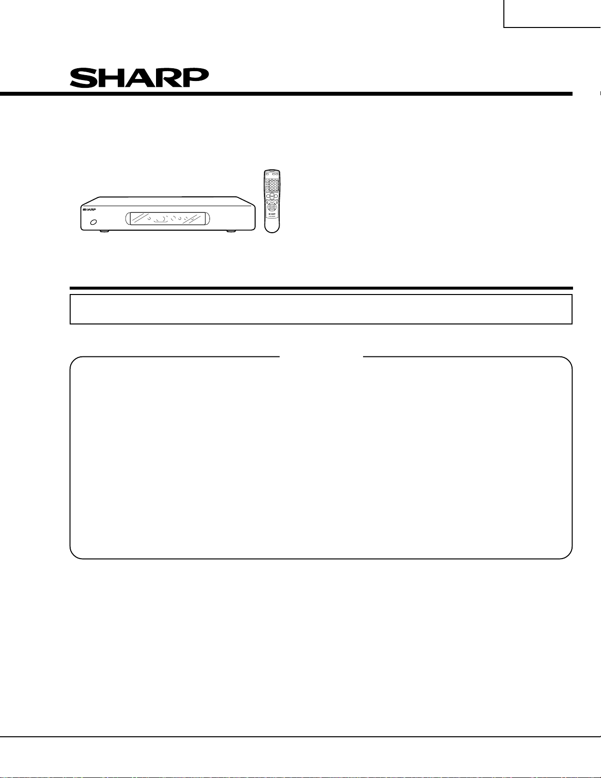
PZ-43MR2E
PZ-50MR2E
SERVICE MANUAL
S12E6PZ50MR2E
PLASMA DISPLAY TV
(AVC SYSTEM)
PZ-43MR2E
MODELS
In the interests of user-safety (Required by safety regulations in some countries) the set should be restored
to its original condition and only parts identical to those specified should be used.
CONTENTS
Page
» IMPORT ANT SER VICE SAFETY PRECAUTION .....2
» SPECIFICATIONS................................................3
» OPERA TION MANUAL ........................................4
» DIMENSIONS ....................................................11
» REMOVING OF MAJOR PARTS........................12
» ADJUSTMENT PROCEDURES.........................14
» DESCRIPTION OF MAJOR IC FUNCTIONS ....20
» TROUBLE SHOOTING TABLE ..........................43
» PRINTED WIRING BOARD BLOCK DIAGRAM .. 50
» SYSTEM BLOCK DIAGRAM ............................. 52
» SIGNAL FLOW BLOCK DIAGRAM....................54
» DC/DC CONVERTER BLOCK DIAGRAM .........56
» POWER BLOCK DIAGRAM............................... 58
» PC I/F BLOCK DIAGRAM ..................................60
» OVERALL WIRING DIAGRAM...........................62
» DESCRIPTION OF SCHEMATIC DIAGRAM ..... 66
» WAVEFORMS .................................................... 67
» SCHEMA TIC DIAGRAM.....................................68
» PRINTED WIRING BOARD ASSEMBLIES...... 108
» P ARTS LIST .....................................................115
» P ACKING OF THE SET ................................... 139
PZ-50MR2E
Page
SHARP CORPORATION
Page 2
PZ-43MR2E
2
2
PZ-50MR2E
IMPORTANT SERVICE SAFETY PRECAUTION
Ë
Service work should be perfomed only by qualified service technicians who are thoroughly familiar with all safety checks and the servicing guidelines which follow:
WARNING
1. For continued safety, no modification of any circuit
should be attempted.
2. Disconnect AC power before servicing.
CAUTION: FOR CONTINUED PROTECTION
AGAINST A RISK OF FIRE REPLACE ONLY WITH
SAME TYPE F701 (T2A, 250V), F702 (T2A, 250V)
AND F1702 (T4AL, 250V) FUSE.
BEFORE RETURNING THE RECEIVER
(Fire & Shock Hazard)
Before returning the receiver to the user, perform
the following safety checks:
1. Inspect all lead dress to make certain that leads are
not pinched, and check that hardware is not lodged
between the chassis and other metal parts in the
receiver.
2. Inspect all protective devices such as non-metallic
control knobs, insulation materials, cabinet backs,
adjustment and compartment covers or shields,
isolation resistor-capacitor networks, mechanical
insulators, etc.
3. To be sure that no shock hazard exists, check for
leakage current in the following manner.
» Plug the AC cord directly into a 110~240 volt AC outlet,
and connect the DC power cable into the receiver's
DC jack. (Do not use an isolation transformer for this
test).
» Using two clip leads, connect a 1.5k ohm, 10 watt
resistor paralleled by a 0.15µF capacitor in series
with all exposed metal cabinet parts and a known
earth ground, such as electrical conduit or electrical
ground connected to an earth ground.
» Use an AC voltmeter having with 5000 ohm per volt,
or higher, sensitivity or measure the AC voltage drop
across the resisor.
» Connect the resistor connection to all exposed metal
parts having a return to the chassis (antenna, metal
cabinet, screw heads, knobs and control shafts,
escutcheon, etc.) and measure the AC voltage drop
across the resistor.
All checks must be repeated with the AC cord plug
connection reversed. (If necessary, a nonpolarized
adaptor plug must be used only for the purpose of
completing these checks.)
Any reading of 35V peak (this corresponds to 0.7
milliamp. peak AC.) or more is excessive and
indicates a potential shock hazard which must be
corrected before returning the monitor to the owner.
DVM
AC SCALE
50k ohm
10W
0.15 µF
TEST PROBE
TO EXPOSED
METAL PAR TS
CONNECT TO
KNOWN EARTH
GROUND
234567890123456789012345678901212345678901234567890123456789012123456789012345678901234567890121
SAFETY NOTICE
Many electrical and mechanical parts in Plasma Display
television have special safety-related characteristics.
These characteristics are often not evident from visual
inspection, nor can protection afforded by them be
necessarily increased by using replacement components
rated for higher voltage, wattage, etc.
Replacement parts which have these special safety
characteristics are identified in this manual; electrical
and shaded areas in the
Schematic Diagrams
For continued protection, replacement parts must be
identical to those used in the original circuit.
The use of a substitute replacement parts which do not
have the same safety characteristics as the factory
recommended replacement parts shown in this service
manual, may create shock, fire or other hazards.
components having such features are identified by “ å”
234567890123456789012345678901212345678901234567890123456789012123456789012345678901234567890121
2
Replacement Parts List
.
and
Page 3
Specifications
Item AVC System, Model: PZ-50MR2E, PZ-43MR2E
Colour System
PAL/SECAM/NTSC 3.58/NTSC 4.43/PAL 60
TV
Function
B/G, D/K, I, L/L’
VHF/UHF E2–E69ch, F2–F10ch, I21–I69ch, IR A–IR Jch
CATV
Hyper-band, S1–S41ch
Auto Channel Preset
99 ch, Auto Preset, Auto Label, Auto Sort
STEREO NICAM/IGR
Terminals SCART (AV in, RGB in, TV out)
INPUT 2
SCART (AV in/out, S-VIDEO in, AV Link)
INPUT 3
SCART (AV in/out, S-VIDEO in, RGB in), Component
ANTENNA 75 q Din Type for VHF/UHF in
INPUT 4 S-VIDEO, AV in
PC INPUT
15 Pin mini D-Sub, Audio in
Audio (Variable, Fixed), S-VIDEO out, AV out
Power Requirement
AC 220–240 V, 50/60 Hz, 40 W (0.8 W Standby)
Dimensions
430 (W), 70 (H), 330 (D) mm
Weight
4.4 kg
Accessories
Power cord, Remote control unit, Two AA size batteries, System cable,
Two operation manuals
Receiving System
Tuner
Rear INPUT 1
Front
• Design and specifications are subject to change without notice.
AV OUTPUT
PZ-43MR2E
PZ-50MR2E
3
Page 4
PZ-43MR2E
PZ-50MR2E
Operation Manual
AVC System
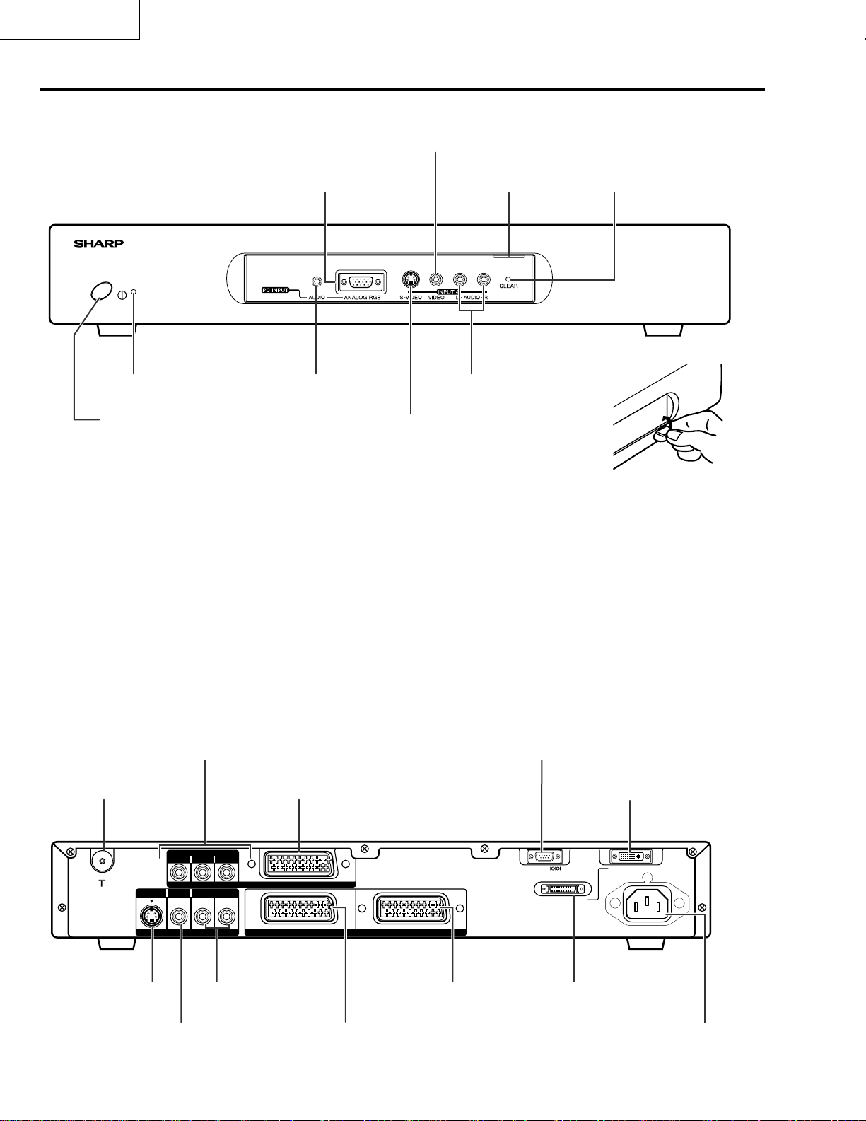
Front view
PC INPUT terminal (ANALOG RGB)
STANDBY/ON indicator
PC INPUT terminal
INPUT 4 terminal (VIDEO)
Door knob
INPUT 4 terminals (AUDIO)
CLEAR button*
(AUDIO)
POWER button
INPUT 4 terminal (S-VIDEO)
(How to open the door)
* If the AVC System is switched on but it does not appear to be operating correctly, it may need resetting. In this
case press CLEAR on the front of the unit as shown in the diagram. Press CLEAR lightly with the end of a
ballpoint pen or other pointed object.
This will reset the System as shown below.
• AV MODE resets to STANDARD
• TV channel resets to channel 1
• Dual screen resets to normal
• Audio setting initialises
• SRS resets to Off
• Image position is initialised
A
• Pressing CLEAR will not work if the System is in standby mode (indicator lights red).
• Pressing CLEAR will not delete channel preset or password. See Page for initialising factory preset settings when you
know your password. See Page or initialising factory preset values when you have forgotten your password.
Rear view
INPUT 3 terminals
(Y, P
B(CB), PR(CR
))
RS-232C terminal
ANTENNA INPUT terminal
S-VIDEO VIDEO
AV OUTPUT
AV OUTPUT terminal
(S-VIDEO)
AV OUTPUT terminal
(VIDEO)
INPUT 3 terminal (SCART)
COMPONENT
PB(CB)
PR(CR)Y
R - AUDIO - L
INPUT 3
AV OUTPUT terminals
(AUDIO)
INPUT 2 INPUT 1
INPUT 1 terminal
(SCART)
INPUT 2 terminal
(SCART)
4
DISPLAY OUTPUT-1 ter minal
RS-232C DISPLAY OUTPUT-1
DISPLAY OUTPUT-2
AC INPUT
220–240V
DISPLAY OUTPUT-2 terminal
AC INPUT terminal
Page 5
PZ-43MR2E
PZ-50MR2E
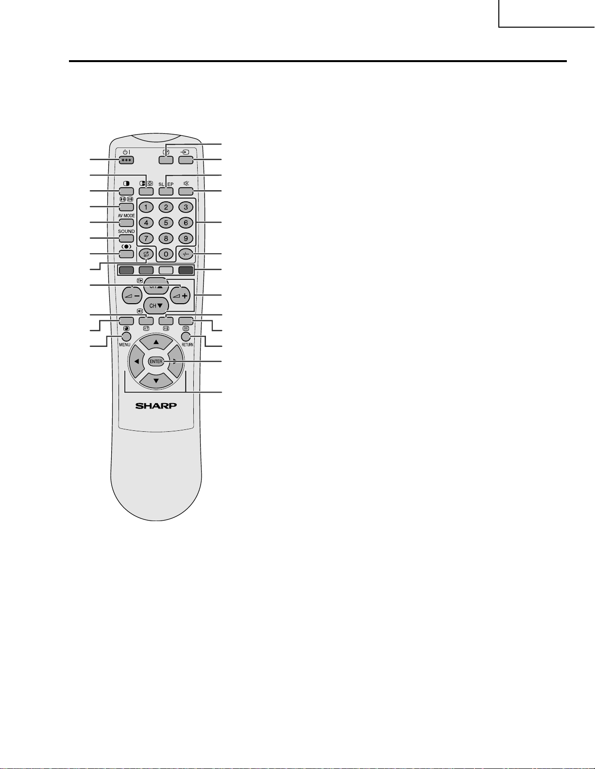
Remote control unit
13
1
2
3
14
15
16
4
5
17
6
7
8
18
19
9
20
10
11
12
21
22
23
24
25
A
• When using the remote control unit, point it
at the Plasma Display TV (Panel Unit).
* “TV”, “INPUT1”, “INPUT2”, “INPUT3”,
“INPUT4” and “PC” modes can each store
the WIDE mode setting separately.
The same for AV mode and volume.
1 a (STANDBY/ON)
To switch the power on and off.
2 du (FREEZE/HOLD for TELETEXT)
TV/External input mode: Change the still image mode.
TELETEXT mode: Freeze a multi-page on screen while other
pages are automatically updated. Press d again to return to the
normal image.
3 c (DUAL screen)
Set the dual picture mode. Press c again to return to normal view.
4 fv (WIDE MODE/ T/B/F)*
TV/External input mode: Change the wide image mode.
TELETEXT mode: Set the area of magnification. (full/upper half/
lower half)
5 AV MODE*
Select a video setting. AV MODE (STANDARD, DYNAMIC, MOVIE,
GAME, USER) PC MODE (STANDARD, USER)
6 SOUND
Select the sound multiplex mode.
7 h (SRS and FOCUS)
Select SRS and FOCUS Sound System.
8 A (FLASHBACK)
Press to return to the previous channel in normal viewing mode.
Press to return to the previous page in TELETEXT mode.
9 il/ik (VOLUME)*
Set the volume.
10 (Reveal hidden for TELETEXT)
k
TELETEXT mode: Display hidden characters.
11 j (SUBPAGE for TELETEXT)
TELETEXT mode: Change the picture mode for sub-page selecting.
12 MENU
Display the Menu screen.
13 C (CHANNEL INFORMATION)
Display the channel information and time.
14 b (INPUT SOURCE)
Select an input source. (TV, INPUT 1, INPUT 2, INPUT 3, INPUT 4,
PC)
15 SLEEP
Set the SLEEP TIMER.
16 e (MUTE)
Mute the sound.
17 0 – 9
TV/External input mode: Set the channel.
TELETEXT mode: Set the page.
18 o (Digit for channel select)
Change the digits of the selected TV channel.
19 Colour (RED/GREEN/YELLOW/BLUE)
TELETEXT mode: Select a page.
20 CHa/CHb(w/x )
TV/External input mode: Select the channel.
TELETEXT mode: Set the page.
21 l (TOP Overview for TELETEXT)
TELETEXT mode: Display an index page for CEEFAX/FLOF
information. TOP OVER VIEW for TOP programme.
22 m (TELETEXT)
Select the TELETEXT mode. (all TV image, all TEXT image, TV/TEXT
image)
23 RETURN
MENU mode: Return to the previous menu screen.
24 ENTER
Execute a command.
Return to the initial image position after moving with a/b/c/d.
25 a/b/c/d (Cursor)
Select a desired item on the setting screen.
Move the picture on the screen.
5
Page 6
PZ-43MR2E
L
PZ-50MR2E
Preparation
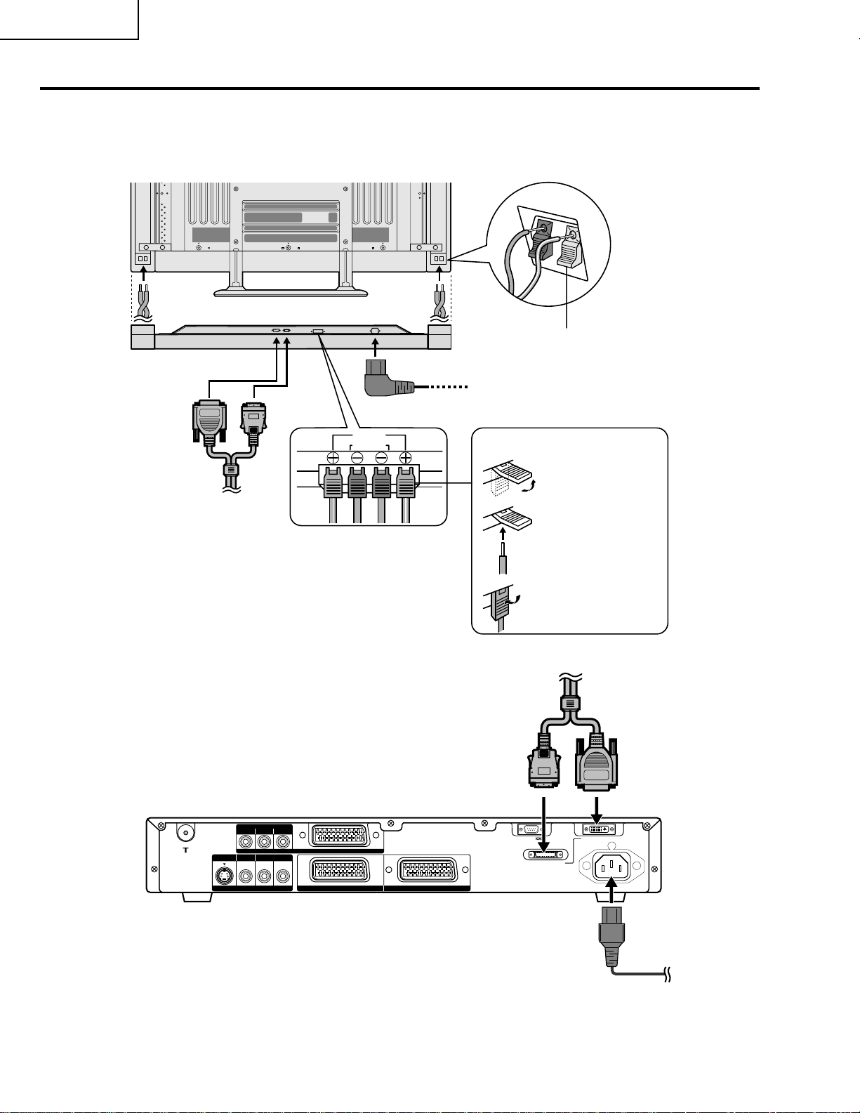
Setting the system
1.
Connecting the system cable, the power cor d and the speaker cables to the Plasma Displa y TV (Panel
Unit)
Plasma Display TV (Panel Unit) (rear view)
Black
Red
Speaker cable
Speaker cable
(bottom view)
(WHITE)
(GRAY)
Red
Black
System cable
Speaker cables
(GRAYeGRAY with white stripe)
A
• Two speaker cables of different lengths are supplied. As
shown in the diagram, connect the longer speaker cable
to the left speaker and the shorter to the right.
2.
Connecting the system cable and the power cord to the AVC System
Power cord
As you apply pressure to this part,
insert the speaker cable. It is
important to match polarity when
connecting the speaker cables to the
terminals.
Insert the speaker cable
Lift up the snap clip.
Insert the wire into
the hole of the
connector.
Lower the snap clip
to grip the wire in
place.
System cable
(GRAY)
(WHITE)
AVC System (rear view)
COMPONENT
PB(CB)
PR(CR)Y
INPUT 3
AV OUTPUT
R - AUDIO - L
INPUT 2 INPUT 1
S-VIDEO VIDEO
• TO PREVENT RISK OF ELECTRIC SHOCK, DO NOT TOUCH UN-INSULATED PARTS OF ANY CABLES WITH THE
POWER CORD CONNECTED.
6
RS-232C DISPLAY OUTPUT-1
DISPLAY OUTPUT-2
AC INPUT
220–240V
Power cord
Page 7
PZ-43MR2E
PZ-50MR2E
preparation
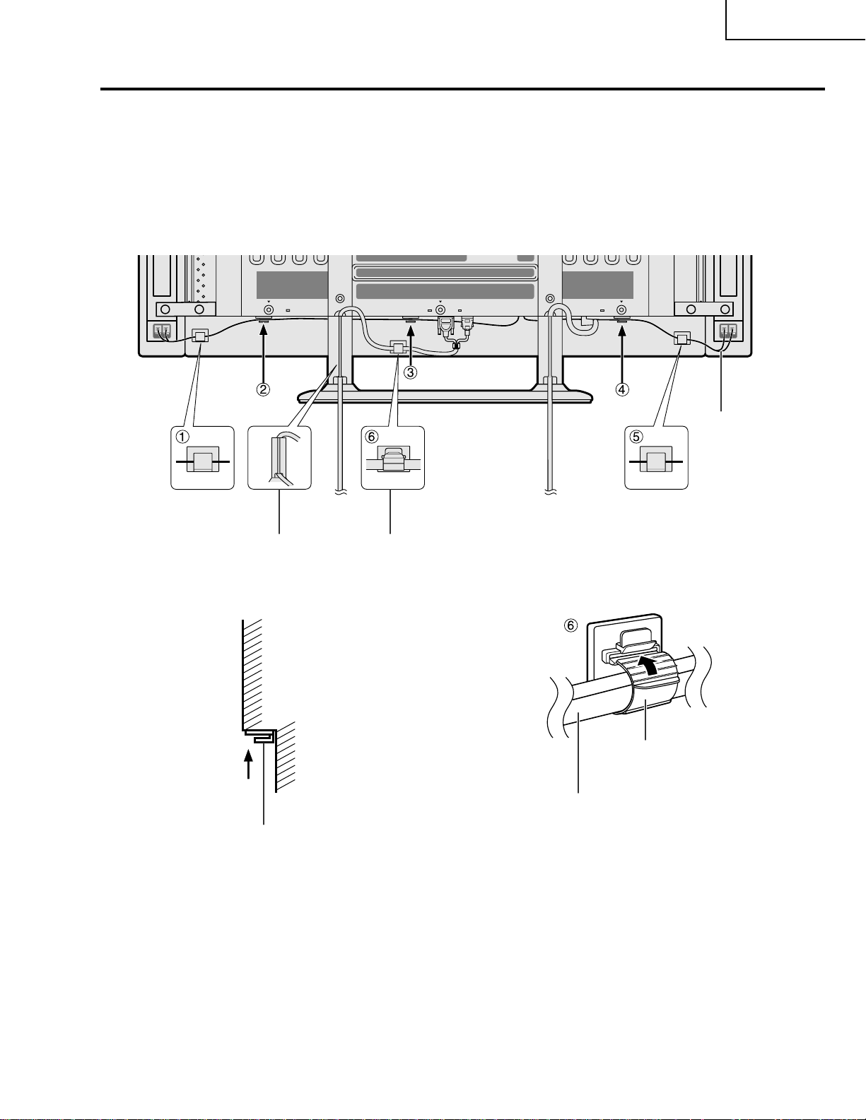
How to route cables
A system cable clamp and five speaker cable clamps are included with the system for cable management. Follow the
diagram below for correct cable management.
As viewed from the rear of the display.
Speaker cable
Speaker cable clamp
Wedge the power cord and the
system cable into the groove on the
stand.
Stick the speaker cable clamps
(2 – 4) to the surface as shown.
System cable
Power cord
Speaker cable clamp
System cable clamp
System cable clamp
System cable
7
Page 8
PZ-43MR2E
L
PZ-50MR2E
preparation
Using the remote control unit
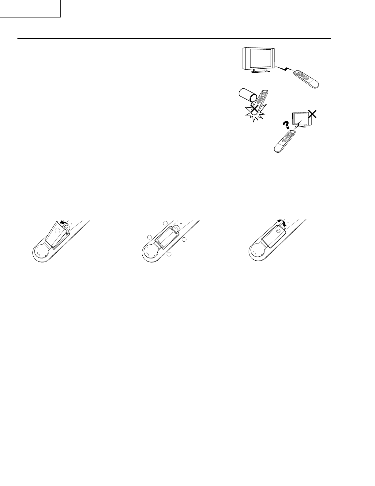
Use the remote control unit by pointing it towards the remote sensor window.
Objects between the remote control unit and sensor window may pr event proper
operation.
Cautions regarding remote control unit
• Do not expose the remote control unit to shock.
In addition, do not expose the remote control unit to liquids, and do not place
in an area with high humidity.
• Do not install or place the remote control unit under direct sunlight.
The heat may cause deformation of the unit.
• The remote control unit may not work properly if the remote sensor window of
the Plasma Display TV (Panel Unit) is under direct sunlight or strong lighting.
In such case, change the angle of the lighting or Plasma Display TV , or operate
the remote control unit closer to the remote sensor window.
Inserting the batteries
If the remote control unit fails to operate Plasma Display TV functions, r eplace the batteries in the remote control
unit.
1
Open the battery cover.
2
Insert batteries (two AA size
batteries, supplied with product).
+
_
• Place batteries with their terminals
corresponding to the (e) and (f)
indications in the battery compartment.
_
+
3
Close the battery cover.
Cautions regarding batteries
Improper use of batteries can result in chemical leakage or explosion. Be sur e to follow the instructions below.
• Do not use manganese batteries. When you replace the batteries, use alkaline ones.
• Place the batteries with their terminals corresponding to the (e) and (f) indications.
• Do not mix batteries of different types. Different types of batteries have different characteristics.
• Do not mix old and new batteries. Mixing old and new batteries can shorten the life of new batteries or cause
chemical leakage in old batteries.
• Remove batteries as soon as they have worn out. Chemicals that leak from batteries can cause a rash. If you
find any chemical leakage, wipe thoroughly with a cloth.
• The batteries supplied with this product may have a shorter life expectancy due to storage conditions.
• If you will not be using the remote control unit for an extended period of time, remove the batteries from it.
• WHEN DISPOSING OF USED BATTERIES, PLEASE COMPLY WITH GOVERNMENTAL REGULATIONS OR
ENVIRONMENTAL PUBLIC INSTRUCTION'S RULES THAT APPLY IN YOUR COUNTRY/AREA.
8
Page 9
PZ-43MR2E
L
PZ-50MR2E
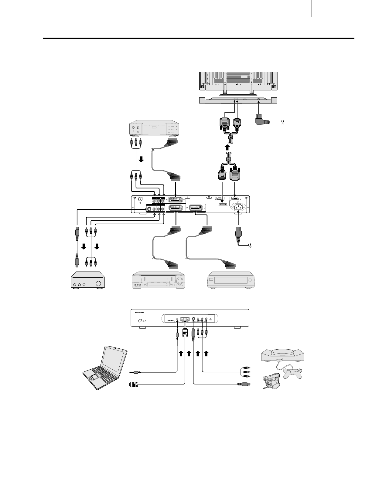
Using external equipment
Y ou can connect many types of external equipment to your Plasma Display TV, like a decoder, VCR, DVD player ,
computer, game console and camcorder. T o view external source images, select the input sour ce fr om b on
the remote control unit or INPUT on the Plasma Display TV (Panel Unit).
Plasma Display TV
(Panel Unit)
(rear view)
(bottom view)
DVD player
Power cord
AV Receiver
(Built-in T uner Amp)
S-VIDEO VIDEO
VCR
AV OUTPUT
COMPONENT
PB(CB)
R - AUDIO - L
PR(CR)Y
INPUT 3
INPUT 2 INPUT 1
RS-232C DISPLAY OUTPUT-1
DISPLAY OUTPUT-2
Decoder
AVC System
(rear view)
AC INPUT
220–240V
Power cord
AVC System
(front view)
Computer
Game console/Camcorder
• To protect all equipment, always turn off the AVC System before connecting to a decoder, VCR, DVD player, computer,
game console, camcorder or other external equipment.
• The S-video signal only outputs when “Input 2” or “Input 3” is selected for “Y/C”, or when from the INPUT 4 terminal (SVIDEO). Only the S-video signal can output from the INPUT 4 terminal (S-VIDEO).
A
• Please refer to the relevant operation manual (DVD player, computer, etc.) carefully before making connections.
9
Page 10
PZ-43MR2E
PZ-50MR2E
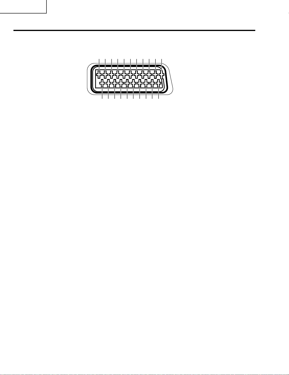
Appendix
Connecting pin assignments for SCART
Various audio and video devices may be connected via the SCART terminals.
13579111315171921
2468101214161820
SCART (INPUT 1)
1. Audio right output
(TV Monitor out)
2. Audio right input
3. Audio left output
(TV Monitor out)
4. Common earth for audio
5. Earth for blue
6. Audio left input
7. Blue input
8. Audio-video control
9. Earth for green
10. Not used
11. Green input
12. Not used
13. Earth for red
14. Not used
15. Red input
16. Red/Green/Blue control
17. Earth for video
18. Earth for Red/Green/Blue
control
19. Video output
(TV Monitor out)
20. Video input
21. Plug shield
SCART (INPUT 2)
1. Audio right output
2. Audio right input
3. Audio left output
4. Common ear th for audio
5. Earth
6. Audio left input
7. Not used
SCART (INPUT 3)
1. Audio right output
2. Audio right input
3. Audio left output
4. Common earth for audio
5. Earth
6. Audio left input
7. Blue input
8. Audio-video control
9. Earth
10. AV LINK control
11. Not used
12. Not used
13. Earth
14. Not used
8. Audio-video control
9. Earth
10. Not used
11. Green input
12. Not used
13. Earth
14. Not used
15. Chroma S-Video input
16. Not used
17. Earth for video
18. Earth
19. Video output
20. Video input/S-video input
21. Plug shield
15. Red input/Chroma S-Video
input
16. Red/Green/Blue control
17. Earth for video
18. Earth
19. Video output
20. Video input/S-video input
21. Plug shield
10
Page 11
Dimensions
PZ-43MR2E
PZ-50MR2E
(Unit: mm)
11
Page 12
PZ-43MR2E
PZ-50MR2E
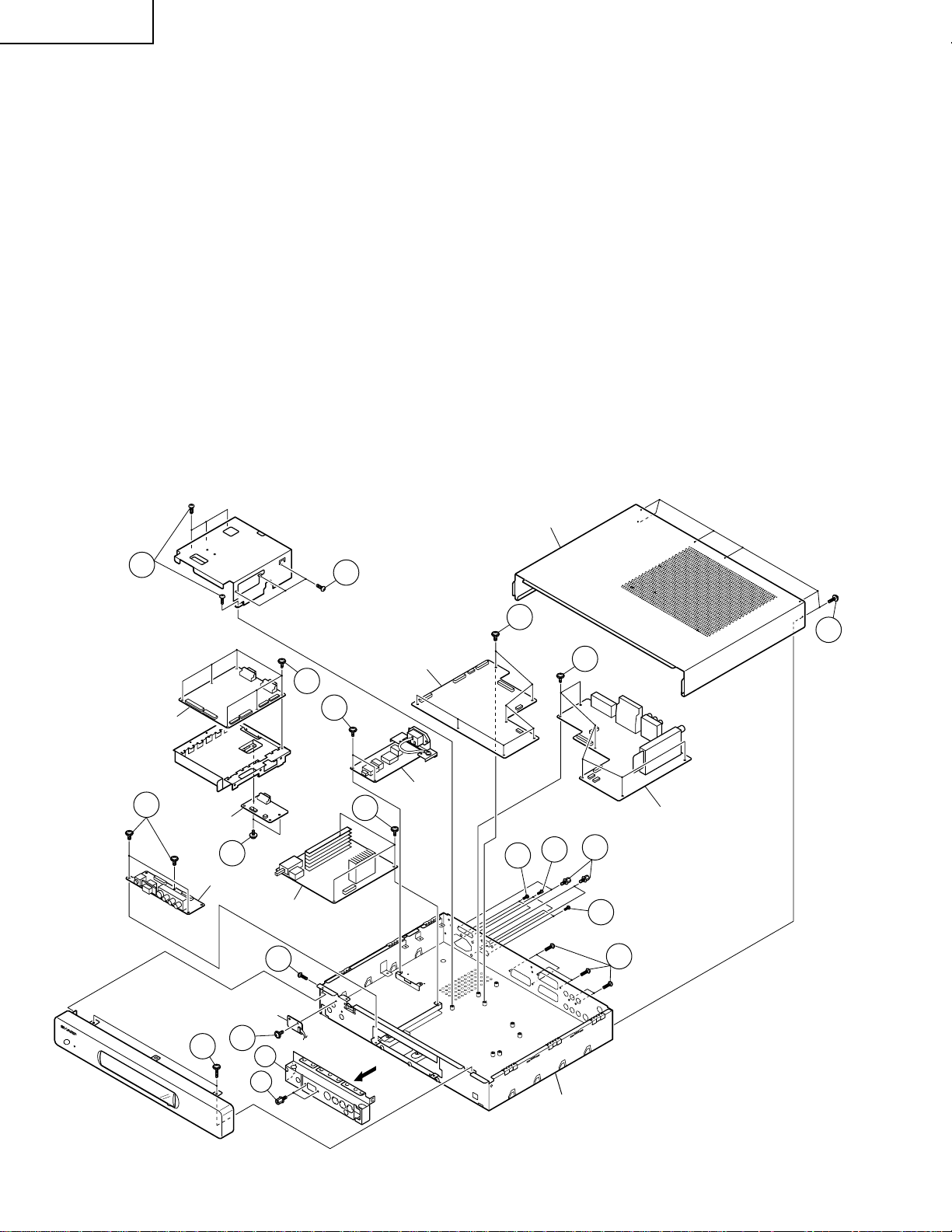
REMOVING OF MAJOR PARTS
1. Remove the six lock screws from the back of the top cabinet. Slide the top cabinet backward and detach it.
2. Remove the three lock screws from the front panel. Undo the three hooks at the top and the four hooks at the
bottom, and detach the front panel.
3. Remove the two hexagonal shafts from the front shield. Undo the two hooks on both sides and detach the
front shield.
4. Remove the three lock screws from the front unit and detach this unit.
5. Remove the one lock screw from the LED unit and detach this unit.
6. Remove the PC I/F unit and SR unit assemblies.
6-1. Remove the two hexagonal shafts each from the system cable (white) terminal and the RS-232C terminal,
both on the PC I/F unit.
6-2. Remove two lock screws from the system cable (gray) terminal also on the SR unit.
6-3. Remove the two lock screws from the PC I/F unit bracket.
6-4. Remove the four lock screws from the PC I/F unit and SR unit assemblies. Take out these assemblies.
6-5. Remove the three lock screws from the brackets of the PC I/F unit and SR unit assemblies. Detach the
shield.
6-6. Remove the six lock screws from the PC I/F unit. Detach this unit from the bracket.
6-7. Remove the two lock screws from the SR unit. Detach this unit from the bracket.
7. Remove the seven lock screws from the main unit and detach this unit.
6-4
PC I/F Unit
4
SR Unit
6-7
Front Unit
6-6
Power Unit
2
9-2
6-5
10
Main Unit
EMC Unit
Top Cabinet
7
9-1
6-3
1
8-2
AV Unit
6-1
6-2
8-1
2
LED Unit
5
11
10
Bottom Cabinet
12
Page 13

8. Remove the AV unit.
8-1. Remove the six lock screws from the AV unit.
8-2. Remove the six lock screws from the AV unit and detach this unit.
9. Remove the EMC unit assemblies.
9-1. Remove the two lock screws from the EMC unit bracket.
9-2. Remove the two lock screws from the EMC unit and detach this unit.
10. Remove the three lock screws from the power unit and detach this unit.
PZ-43MR2E
PZ-50MR2E
13
Page 14

PZ-43MR2E
PZ-50MR2E
ADJUSTMENT PROCEDURES
Ë
Procedure for turning ON the power
1. Connecting the system
» Using the system cable, connect the Panel Unit and the AVC System.
» Connect the Panel Unit to the AC power source.
» Connect the AVC System to the AC power source.
2. Procedure for turning ON the power
» Turn ON the AC power switch located on the Panel Unit.
The STANDBY/ON indicator on the Panel Unit will start blinking in red.
(When the AC POWER button on the AVC System is not ON, the STANDBY/ON indicator on the Panel Unit
always blinks in red.)
» Turn ON the POWER button located on the AVC System.
The ST ANDBY/ON indicator on the AVC System will be illuminated in green. Simultaneously , the power indicator
on the Panel Unit will change from blinking in red to illumination in green. Now the system has started up.
» If the STANDBY/ON indicator on the AVC System is illuminated in red, press the POWER button located on the
remote control unit and the MAIN POWER button located on the Panel Unit. The STANDBY/ON indicators on
the Panel Unit and the AVC System will change from red to green. Now the system has started up.
Ë
Procedure for upgrading the software
(1)With the power being OFF, open the top cabinet for the AVC System and then set the slide switch from the
NORMAL position to the WRITE position by inserting a needle-like insulator into the cutout located between
the WHITE port on the rear of the shield case for the PC I/F unit and the RS-232C port.
(2)Connect the PC having the program installed, to the AVC System using the cross cable for the RS-232C port
(for the details of the program, see Appendix).
(3)Open the MS-DOS window on the PC and then go to the directory in which the software is installed.
(4)Start up the system to which the AVC System and Panel Unit have been connected.
(5)Run “vup.bat (tentaive name)” at the MS-DOS prompt. The software will be upgraded.
(6)Load the file “civc_XXXXa.bhxmain.bhxosd.bhxt (tentaive name)”. It will take approximately a few minutes
until the file has been loaded. Never turn OFF the power or operate the system during this rewriting period.
(7)After the file has been loaded, turn OFF the Panel Unit and the AVC System and then return the slide switch in
the above step 1 from the WRITE position to the NORMAL position. Now the software has been upgraded.
Ë
Procedure for adjusting each part of AVC System
» The adjustments were made to the best settings at factory. If any setting deviates or if any readjustment is
regarded as necessary when any part is replaced, perform the following steps.
» Any parameter that has been changed within the process adjustment is stored on the memory . If any readjustment
is required, write down the current value before changing it.
» Use a stable AC power source.
» If the program is upgraded, it will take approximately 1 minute for the EEPROM to be initialized before any video
appears. Therefore, you will need to wait for this time period. Do not turn OFF the power or operate the system
during the period.
» If the program is rewritten, write down the parameters that have been changed within the process adjustment
(see “5”.OSD menu and parameters displayed at manual adjustment), initialize the EEPROM, and then reenter
the recorded values.
14
Page 15

3. Entering a special mode
1 Entering the process adjustment mode
[Steps]
(1)When using the remote control unit:
Using the system cable, properly connect the Panel Unit and the AVC System, and then turn ON the
power.
After the system has started up, press the PROCESS ADJ button located on the remote control unit.
(2)When using buttons on the main unit:
Using the system cable, properly connect the Panel Unit and the AVC System.
Turn ON the power while holding down the INPUT and CH UP buttons located the Panel Unit.
[Description]
Various adjustments can be made manually.
2 Entering the inspection process mode
[Steps]
After the system has started up, press the PROCESS ADJ button located on the remote control unit.
Set the parameter SIGNAL INFO to 1 on page 6 or 7 of the PROCESS ADJUSTMENT A MODE MENU.
Subsequently, make the necessary adjustments in accordance with the above menu.
3 Procedure for setting up delivery
[Steps]
After the system has started up, press the DELIVERY SETUP button located on the remote control unit.
(Within the adjustment process, the channel settings remain unchanged. Once you exit the process adjustment
mode, the channel settings entered in the delivery adjustment mode become valid.)
[Description]
The user’s adjustment parameters and others will be set to the default values. The channel settings will also
be initialized.
PZ-43MR2E
PZ-50MR2E
4. Exiting a special mode
(1)Process adjustment mode: Press the PROCESS ADJ button located on the remote control unit or turn OFF the
power.
(2)Inspection process mode: Set the parameter SIGNAL INFO to 0 on page 6 or 7 of the PROCESS ADJ A MODE
MENU or turn OFF the power.
(3)Delivery setup: After the delivery setup has been finished, the process adjustment mode is automatically
selected. To exit the process adjustment mode, press the PROCESS ADJ button located on the remote control
unit or turn OFF the power.
5. OSD menu and parameters displayed at manual adjustment
* The default values may slightly differ depending upon the program version to be rewritten.
* The settings are not initialized to the default values by merely rewriting the program. (See the paragraph for
Preparation for adjustment.)
(1)Descriptions of special buttons in process adjustment mode
Cursor UP key : Proceeds to the previous page.
Cursor DOWN key: Returns to the next page.
VOL UP key : Increases the adjusted value by 1.
VOL DOWN key : Decreases the adjusted value by 1.
Cursor LEFT key : Decreases the adjusted value by 10.
Cursor RIGHT key : Increases the adjusted value by 10.
CH UP key : Moves up the cursor.
CH DOWN key : Moves down the cursor .
15
Page 16
PZ-43MR2E
PZ-50MR2E
Ë
Organization of process adjustment screen
Page Input Source HDCP
INPUT1 No SIG1/16 HDCP:ON EUROPE EUROPE
Maker Select
Ë +Badj3.3V
Ë +Badj2.5V
KEY WRITE
Ë DATA COPY
INDUSTRY INIT
CENTER Version
OSD Version
CVIC Version
TTXP V ersion
MONITOR Version
PANEL Version
FLASH Version
MONITOR Model
Model Select MONITOR
STANDBY TYPE
SHARP
127
024
OFF
OFF
OFF
MR MAIN E 2001/11/28K
MR OSD 2001/09/10 A
W2001/10/02 17:28 X2001/10/02 V2001/09/12 09:12
TTX PRG 068
F6 91 xx
-00
-05
01
1
0
Destination for MAIN unit Destination for AV unitDistinguish Signal
Parameter display
Ë
+B Adj3.3V
Ë
+B Adj2.5V
Ë
P AL Y CONTRAST
Ë
PAL COLOR GAIN
Ë
MAIN CR GAIN PAL
Ë
MAIN SUBBRIGHT 15K
Ë
MAIN CONTRAST 15K
Ë
SUB P AL Y
Ë
SUB PAL COLOR GAIN
Ë
PEAK ACL SW
Ë
SECAM Y CONTRAST
Ë
SECAM COLOR GAIN
Ë
MAIN CR GAIN SECAM
Ë
N358 Y CONTRAST
Ë
N358 COLOR GAIN
Ë
MAIN CR GAIN N358
Ë
N358 TINT
Ë
COMP 15K Y CONTRAST
Ë
COMP 15K COLOR GAIN
Ë
MAIN CR GAIN COMP15K
Ë
COMP HDTV SUB BRIGHT
Ë
COMP HDTV CONTRAST
Ë
DA TA COPY
Setting range
0 ~ 255
0 ~ 255
0~ 63
0~ 63
0 ~ 255
0~ 63
0~ 15
-30 ~ 30
0~ 63
OFF/ON
0~ 63
0~ 63
0 ~ 255
0~ 63
0~ 63
0 ~ 255
-30 ~ 30
0~ 63
0~ 68
0 ~ 255
0~ 63
0~ 15
OFF/ON
Description
3.3 V adjustment
2.2 V adjustment
P AL Y level adjustment
PAL colour density adjustment
P AL Cr level adjustment
Pedestal level adjustment (15 k)
PCB input amplitude adjustment (15 k)
Sub P AL Y level adjustment
Sub PAL colour density adjustment
SECAM Y level adjustment
SECAM colour density level adjustment
SECAM Cr level adjustment
N358 Y level adjustment
N358 colour density adjustment
N358 Cr level adjustment
N358 tone adjustment
COMP 15 k Y level adjustment
COMP 15 k colour density adjustment
COMP 15 k Cr level adjustment
COMP HDTV black level adjustment
COMP HDTV Y level adjustment
COMP HDTV colour density adjustment
The values for the above parameters should be written down before the EEPROM is replaced on
the AVC system.
Note: The contents on the adjustment process menu may be somewhat different depending on
the program's version-up.
16
Page 17
PZ-43MR2E
PZ-50MR2E
6. Procedures before and after replacing the PC I/F unit
1) Before replacing the PC I/F unit, write down the values for the parameters listed on the 2nd and 3rd pages of
the Adjustment Process A screen.
If the values for the parameters cannot be written down because the PC I/F unit is completely broken or for any
other reason, make all the adjustments in accordance with the paragraph for Adjustment procedure and
parameters, rather than the following procedures. (End)
Set the parameters listed on the 2nd and 3rd pages of the Adjustment Process A screen to the values you have
written down.
7. Adjustment parameters
1) Analog adjustment
(1) Prior adjustment for AVC system chassis
Adjustment item Description Adjustment procedure
1 Destination check 1. Call the process adjustment mode.
2. Check that the destination is “Europe”.
2 AVC center 3.3V
adjustment
3 AVC center 2.5V
adjustment
Connect DC voltmeter to
TP1702.
Connect DC voltmeter to
TP1701.
Adjust output voltage of DC/DC 5 V line to
3.3 V .
Adjusted value: 3.25~3.29 V
Adjust output voltage of DC/DC 2.5 V line to
2.6 V .
Adjusted value: 2.60~2.64 V
(2) PAL signal adjustment
Adjustment item Description Adjustment procedure
1 Setup 1. Set colour system to “PAL”.
2. Select PAL source.
100% colour bar signal including 100% white, such
as split field colour bar
2 Tuner Y level
adjustment
3 PAL Y CONTRAST
adjustment
4 PAL COLOR GAIN
adjustment
1. Adjust TP1101 so that the Y signal without the
chroma component should be 1.00 ±0.05 Vp-p
(between the bottom of sync signal and the white
peak).
1. Adjust TB1274_MAIN output (TP803) to
0.7 ±0.05 Vp-p.
1. Adjust TB1274_MAIN
output (TP802) to
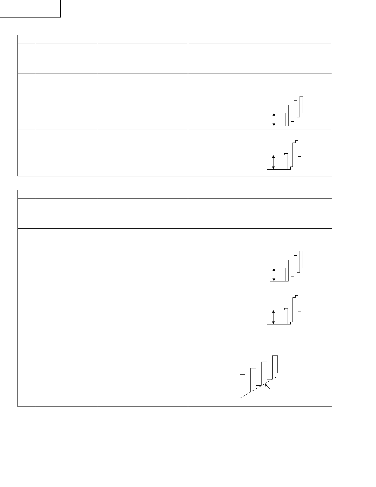
0.35 ±0.025 Vp-p.
0.35V
5 MAIN CR GAIN PAL
adjustment
6 MAIN CONTRAST
adjustment
Press the DUAL screen button. Select the special DUAL screen settings for adjustment
7 SUB PAL Y adjustment 1. Adjust TB1274_SUB output (TP806) to
8 SUB PAL COLOR
GAIN adjustment
1. Adjust TB1274_MAIN output
(TP801) to 0.35 ±0.05 Vp-p.
0.35V
Turn off the PEAK ACL control. Adjust the output
(TP815) of IC810 to have 1.1 ±0.05 Vp-p from the
pedestal level.
(so that the same video source is reflected on MAIN/
SUB).
0.9 ±0.05 Vp-p.
1. Adjust TB1274_SUB output (TP805) to
0.9 ±0.05 Vp-p.
17
Page 18
PZ-43MR2E
0.35V
0.35V
0.35V
0.35V
PZ-50MR2E
(3) SECAM signal adjustment
Adjustment item Description Adjustment procedure
1 Setup 1. Set colour system to SECAM.
2. Select SECAM source.
100% colour bar signal including 100% white, such
as split field colour bar
2 SECAM Y CONTRAST
adjustment
3 SECAM COLOR GAIN
adjustment
1. Adjust TB1274_MAIN output (TP803) to
0.7 ±0.05 Vp-p.
1. Adjust TB1274_MAIN
output (TP802) to 0.35
±0.025 Vp-p.
4 MAIN CR GAIN
SECAM adjustment
1. Adjust TB1274_MAIN
output (TP801) to 0.35
±0.025 Vp-p.
(4) N358 signal adjustment
Adjustment item Description Adjustment procedure
1 Setup 1. Set colour system to N358.
2. Select N358 source.
100% SMPTE colour bar or similar colour bar
signal including 100% white.
2 N358 Y CONTRAST
adjustment
3 N358 COLOR GAIN
adjustment
4 MAIN CR GAIN N358
adjustment
1. Adjust TB1274_MAIN output (TP803) to
0.7 ±0.05 Vp-p.
1. Adjust TB1274_MAIN
output (TP802) to 0.35
±0.025 Vp-p.
1. Adjust TB1274_MAIN
output (TP801) to 0.35
±0.025 Vp-p.
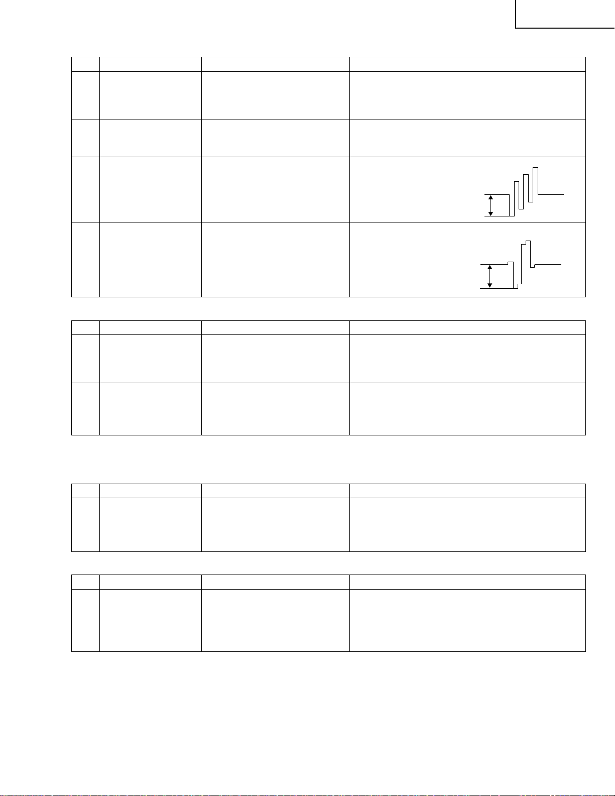
5 N358 TINT adjustment 1. Adjust TB1274_MAIN output (TP802) so that
waveform becomes as illustrated below:
Smoothed
18
Page 19
(5) Component 15k Hz signal adjustment
Adjustment item Description Adjustment procedure
1 Setup 1. Select component 15k Hz.
2. Select component source.
100% colour bar signal including 100% white, like
split field colour bar
2 COMP 15k
CONTRAST
adjustment
3 COMP 15k COLOR
GAIN adjustment
Adjust TB1274_MAIN output (TP803) to 0.7 ±0.05 Vp-p.
Adjust TB1274_MAIN output
(TP802) to 0.35 ±0.025 Vp-p.
PZ-43MR2E
PZ-50MR2E
0.35V
4 MAIN CR GAIN COMP
15k adjustment
Adjust TB1274_MAIN output
(TP801) to 0.35 ±0.025 Vp-p.
0.35V
(6) Component HDTV signal adjustment
Adjustment item Description Adjustment procedure
1 Setup 1. Input HDTV (1080i) component signal.
2. Select component source.
100% colour bar signal including 100% white, like
split field colour bar
2 COMP HDTV
CONTRAST
adjustment
Turn off the PEAK ACL control.
Adjust the output (TP815) of pin (11) of IC810 to have
1.1 ±0.05 Vp-p from the pedestal level.
2. Factory settings
(1) Data Copy
Adjustment item Description Adjustment procedure
1 DATA COPY 1. Using the adjustment key, set “ON” in the DATA
COPY line. Wait until “OFF” is displayed instead.
Finally turn off the power to quit the process
adjustment mode.
(2) Factory Setting
Adjustment item Description Adjustment procedure
1 INDUSTRY INIT Move the cursor to the INDUSTRY INIT line. Using the
Vol.UP key, turn off and on again, and press ENTER. "/
/////////" appears, telling that the program is now being
settings are complete. Be sure to wait until the sign
goes out.
* Then turn off the AC power supply of the AVC system. (Be careful not to use the power switches of the remote control unit
and A VC system.)
19
Page 20

PZ-43MR2E
PZ-50MR2E
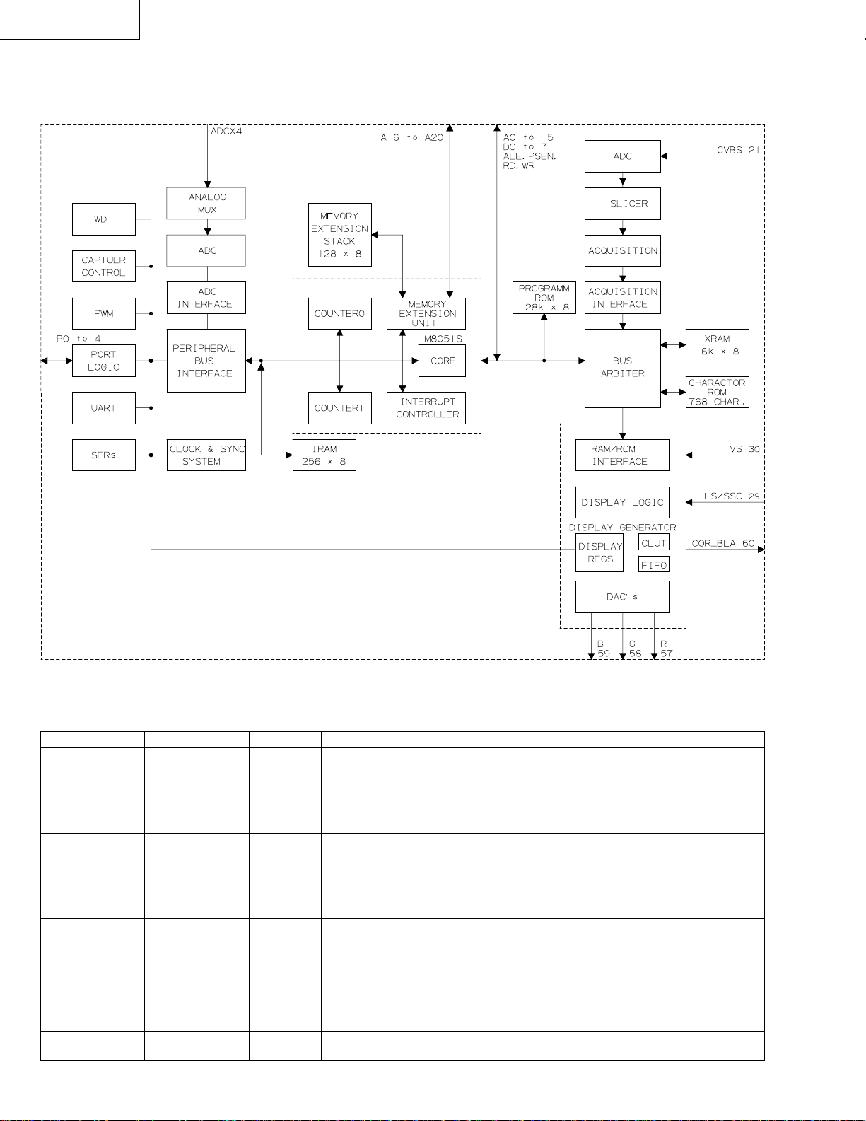
DESCRIPTION OF MAJOR IC FUNCTIONS
Æ Description of Main ICs
»»
» IC1301 (CXA2069Q)
»»
This IC is a 7-input, 3-output selector.
The video signals other than those for the PC, components and RGB input, which have been input from each input
connector and the tuner, and all the audio signals are sent to the IC1301 and then selected.
Output 1 is used internally and output 3 in the monitor output.
When the S video input is output to the monitor, Y and C signals are mixed in this IC.
The video signals sent to the IC1301 are then input to the YC separation circuits, IC405 (main) and IC402 (sub).
The audio signals are input to the PC I/F Unit via IC2501 (sound processor).
»»
» IC1401 (MM1519XQ)
»»
This IC is a 4-input, 8-output video selector for component input.
The AV3 component input, AV1, RGB input, and Teletext RGB signals are input to the IC1401. The output signals
go to the main, sub, and component channels.
»»
» IC1601 (SDA5550M).
»»
This IC is a microprocessor for Teletext.
Video signals are input to the IC1601, which then decodes the Teletex data and outputs it as RGB data.
»»
» IC2501 (IX3371CE)
»»
This IC is used to decode audio signals.
It serves as both the S IF decoder and the selector for the input audio data.
»»
» IC801/IC802 (TB1274AF)
»»
This IC synchronizes video and chroma signals for PAL/NTSC/SECAM colour televisions.
Its video circuit includes a high-performance image quality compensation circuit and its chroma circuit a PAL/
NTSC/SECAM automatic selection circuit. The P AL-M/N clock signals at 4.43 and 8.58 MHz are internally generated
for colour demodulation.
The PAL/SECAM demodulation circuit uses a base band signal processing system with built-in IH DL and is
therefore adjustment-free.
The IC801/IC802 has 4 lines for YC signal input, 2 lines for RGB signal input, and 2 lines for colour difference
signal input. It receives colour different signals for the main and sub channels from IC405 (main), IC402 (sub), and
IC1401 in the former stage, and provides 1 line for colour difference signal output.
»»
» IC803 (CXA2101Q)
»»
This IC consists of a base band signal processing section for colour different input, an RGB signal processing
section, and a 4-line video switch (including HV synchronizing signal processing).
Input selection is performed by INPUT-SEL (I2C BUS). YCbCr , HD YPbPr , GBR and their respective HV synchronizing
signals are input to each line.
As the multi-scanning compliance range, a horizontal scanning frequency of 15~60 kHz can be input.
»»
» IC1901 (IX3566CE)
»»
This IC is FPGA for the synchronizing system.
It creates sand castle pulses for IC803 and generates horizontal blanking signals.
»»
» IC604 (TA1318AF)
»»
This IC synchronizes TV component signals.
The IC804 incorporates the necessary functions for measuring the frequency of input signals and synchronous
replay into a single chip, and is applicable for horizontal synchronous replay (15.75, 31.5, 33.75, and 45 kHz) and
vertical synchronous replay (525I, 525P, 625I, 750P, 1125I, 1125P, PAL 100 Hz, and NTSC 120 Hz).
20
Page 21

PZ-43MR2E
PZ-50MR2E
»»
» IC405/IC402 (CXD2064Q)
»»
This IC is a comb filter in the applicable field for both the NTSC and P AL systems. It performs the Y/C separation
of the main and sub channel video signals that have been output from IC1801.
»»
» IC407/IC404 (ML6428C1)
»»
This IC is a 6.7 MHz low-pass filter.
»»
» IC810/IC804 (IX3473CE)
»»
This IC is a 6.7 MHz low-pass filter incorporating a 6 dB amplifier.
»»
» IC811 (IX3474CE)
»»
This IC is a 30 MHz low-pass filter incorporating a 6 dB amplifier.
»»
» IC1702 (FA3675CE)
»»
This IC is designed to control the 6-channel PWM switching regulator.
With 5 step-up switching regulator lines incorporated, the IC converts +10V to +2.5V, +3.3V and +5.8V.
Also with a step-down switching regulator line incorporated, the IC converts +10V to +6.0V , -5.0V, +12V and +35V .
The lines are individually turned on and off.
Æ
Description of Functions of Main ICs on PC I/F Unit
»»
» IC4 (CXA3506R)
»»
This IC is an A/D converter that incorporates a 3-channel, 8-bit, 120 MSPS amplifier and PLL. It is used for the
video signals input to the PC I/F unit on the main channel in the 1-screen and 2-screen modes, and also for the
video signals input from the front for the PC.
The video signals (analog RGB) from the CN6 are input to IN1 of IC4.
For the PC, the video signals (analog RGB) from CN8 are input to IN2 of IC4.
The input video signals are converted into digital signals and then sent to IC25.
»»
» IC310 (TLC5733A)
»»
This IC is a 3-channel, 8-bit, 20 MSPS A/D converter.
It is used for the sub-channel of the video signals input to the PC I/F Unit in the 2-screen mode.
The video signals (analog Y, Cb, Cr) from CN6 are input to IC310.
The video signals input to this IC are converted into digital signals and then sent to IC25.
»»
» IC25 (IX3434CE)
»»
This IC performs the I/P conversion and scaling to match the digitalized video with the output resolution, and also
the data conversion.
It has two input lines, V0 and V1. The V0 line is used to process the RGB, composite, and skirt signals input to the
480i and 580i components for the sub-channel in the 2-screen mode. The V1 line is used to process all the signals
as well as V1 for the main channel in the 1-screen and 2-screen modes.
The IC25 detects what resolution is input from the input synchronizing signal; creates H synchronization in
accordance with the frequency division ratio; creates the clamp signal in accordance with the input synchronizing
signal; and performs the data matrix conversion.
The video signals input to this IC is sent to IC413.
»»
» IC413 (SiI168)
»»
This IC is a panel link transmitter.
It converts the 8-bit RGB video data output from IC25 into the differential TMDS signals and then digitally transmits
the converted signals to the monitor.
The TMDS signals are transmitted at the frequency 10 times higher than the clock frequency.
»»
» IC1 (IX3270CE)
»»
This IC is a 1-chip RISC microprocessor.
It performs communication with the monitor and operates the system.
The IC1 also controls each IC in the AVC system and partially manages the power source.
»»
» IC405 (uPD4721)
»»
This IC is an RS-232 line driver receiver conforming to the EIA/TIA-232-E standard.
The IC405, when connected to a PC, allows for externally controlling the system.
It is also applicable for upgrading IC1.
21
Page 22
PZ-43MR2E
PZ-50MR2E
» The information shown in the list is basic information and may not correspond exactly to that shown in the schematic diagrams.
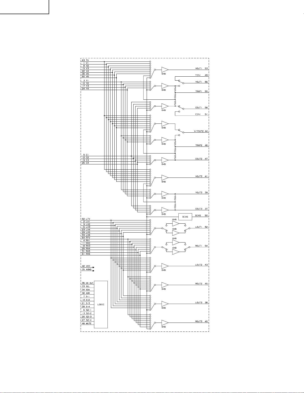
Ë VHiCXA2069Q-1 (ASSY: IC1301)
» S2-Compatible, 7-Input/3-Ouput AV Switch
» Block Diagram
22
Page 23
» Pin Function
Pin No. Pin Name I/O Pin Function
63
1
8
15
22
30
60
3
10
17
24
49
5
12
19
26
51
62, 2
9, 16
23, 29
59, 64
4, 11
18, 25
31, 61
53
41
44
56
39
58
47
37
52
43
38
54
45
40
6
13
20
27
7
14
21
28
32
33
34
36
55
46
48
50
TV
V1
V2
V3
V4
V5
V6
Y1
Y2
Y3
Y4
YIN1
C1
C2
C3
C4
CIN1
LTV, LV1
L V2, LV3
L V4, LV5
L V6, RTV
RV1, RV2
RV3, RV4
RV5, RV6
VOUT1
VOUT3
V/YOUT2
YOUT1
YOUT3
COUT1
COUT2
COUT3
LOUT1
LOUT2
LOUT3
ROUT1
ROUT2
ROUT3
S2-1
S2-2
S2-3
S2-4
S-1
S-2
S-3
S-4
ADR
SCL
SDA
DC OUT
TRAP1
TRAP2
MUTE
BIAS
I
I
I
I
I
I
I
I
I
I
I
I
I
I
I
I
I
I
I
I
I
I
I
I
O
O
O
O
O
O
O
O
O
O
O
O
O
O
I
I
I
I
I
I
I
I
I
I
I
O
I
I
I
I
Video signal input.
Composite video signal input
Y/C-separated signal input terminal for luminance signal input.
YIN1 to feed in the Y/C-separated signal of VOUT1 output.
Y/C-separated signal input terminal for chrominance signal input.
CIN1 to feed in the Y/C-separated signal of VOUT1 output.
Audio signal input terminal.
Video signal output terminal for composite video signal output.
Video signal output terminal for selection between composite video signal output and
luminance signal output by I2C Bus control.
Video signal output terminal for luminance signal output.
Video signal output terminal for chrominance signal output.
Audio signal output terminal.
Used to detect C signal-superimposed, S2-compatible DC level. 4:3 video signal when
below 1.3V. 4:3 letterbox signal when between 1.3V and 2.5V . 16:9 image squeeze
signal when above 2.5V. To be pulled down to GDN at 100KΩ to produce 4:3 video
signal when open.
Used to switch between composite video and S signals. Detection results to be written
in status register. S signal when below 3.5V. Composite video signal when above 3.5V.
To be pulled up to 5V at 100KΩ to produce composite video signal when open.
Used to select I2C Bus slave address. 90H when below 1.5V. 92H when above 2.5V.
90H also when the terminal is open.
I2C Bus signal input terminal.
I2C Bus signal input terminal.
Used to feed out S2-compatible DC level to be superimposed on COUT3 output. DC to
be superimposed by connecting to COUT3 output via a capacitor. Control to be made
by I2C Bus. S2-specified output impedance of 10 ±3KΩ to be realized by adding an
external resistance of 4.7KΩ.
Subcarrier trap circuit to be connected.
Audio signal output mute terminal. Mute off when below 1.3V. Mute on when above
2.5V. Mute off when the terminal is open.
Internal reference bias (Vcc/2) terminal. To be connected to GND with a capacitor in
between.
PZ-43MR2E
PZ-50MR2E
23
Page 24
PZ-43MR2E
PZ-50MR2E
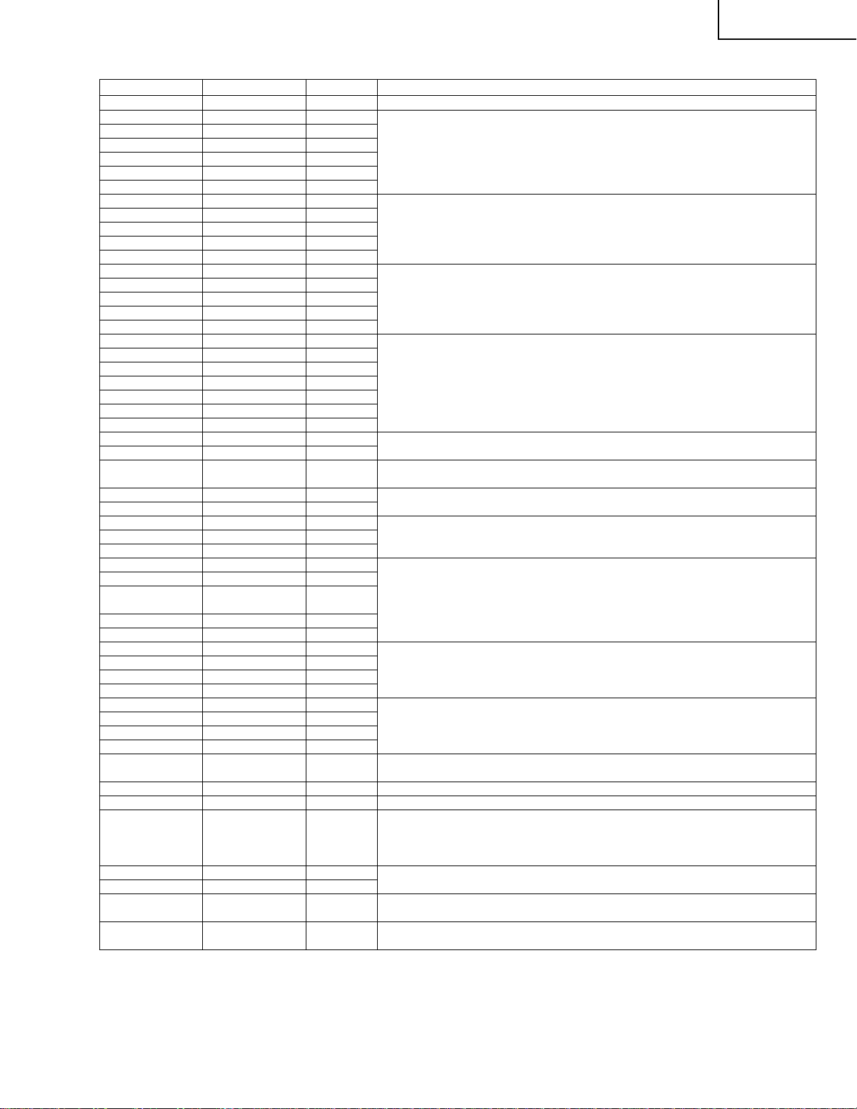
Ë VHiMM1519XQ-1(IC1401)
» Component Input Video Switch
» Block Diagram
24
Page 25
» Pin Function
Pin No. Pin Name I/O Pin Function
1
2
3
11
12
13
21
22
23
4, 14, 39, 45, 52,
58
51
5
15
53
59
24
6, 8, 16, 18, 33,
35, 37, 41, 43, 47,
49, 54, 56, 60, 62
7
9
17
19
55
57
61
63
10
20
32
64
25
26
27
28
29
30
31
34
36
38
40
42
44
46
48
50
VIDEO 1-L1
VIDEO 1-L2
VIDEO 1-L3
VIDEO 2-L1
VIDEO 2-L2
VIDEO 2-L3
VIDEO 3-L1
VIDEO 3-L2
VIDEO 3-L3
VCC
AVCC
VIDEO 2-Y
VIDEO 3-Y
TUNER-Y
VIDEO 1-Y
DGND
GND
VIDEO 2-Pb
VIDEO 2-Pr
VIDEO 3-Pb
VIDEO 3-Pr
TUNER-Pb
TUNER-Pr
VIDEO 1-Pb
VIDEO 1-Pr
VIDEO 2-SW
VIDEO 3-SW
MONO-SW
VIDEO 1-SW
ADDRESS
SDA
SCL
DVCC
L3 OUT
L2 OUT
L1 OUT
Pr OUT 3
Pb OUT 3
Y OUT 3
Pr OUT 2
Pb OUT 2
Y OUT 2
Pr OUT 1
Pb OUT 1
Y OUT 1
—
—
—
—
I/O
—
I
I
I
I
I
I
I
I
I
I
I
I
I
I
I
I
I
I
I
I
I
I
I
I
I
I
I
O
O
O
O
O
O
O
O
O
O
O
O
Line input of D-terminal
Analog power supply (9V)
Y -signal input
GND
Pb, Pr signal input
Switch line of D-terminal
Slave address select pin
Data input of I2C bus
Clock input of I2C bus
Digital power supply (5V)
Line output for monitor
Video signal output
PZ-43MR2E
PZ-50MR2E
25
Page 26
PZ-43MR2E
PZ-50MR2E
Ë VHiSDA5550M-1 (ASSY: IC1601)
» Stereo Audio DAC
» Block Diagram
» Pin Function
Pin No. Pin Name I/O Pin Function
99, 1, 3, 4, 2, 100,
98, 96
97, 94, 93, 89, 86,
84, 82, 79, 81, 83,
90, 85, 77, 78, 76,
71, 69
70, 68, 67
9, 10, 11, 12, 13,
14, 15, 16
41, 42, 43, 44, 45,
46, 47, 62
24, 25, 26, 27
D0-D7
A0-A16
A17-A19/
P4.0, P4.1, P4.4
P0.0-P0.7
P1.0-P1.7
(PWM)
P2.0-P2.3
(ADC)
I/O
O
I/O
I/O
I/O
Data bus for external memory or data RAM.
Address bus for external program memory or data RAM.
After power-on P4.0,P4.1,P4.4 work as additional address lines A17…A19.
In port mode, these port lines act as bi-directional I/O port with internal pull-up
resistors. Port pins that have ‘1’ written to them are pulled high by the internal pull-up
resistors and in that state can be used as inputs.
Port 0 is a 8-bit open drain bi-directional I/O-port. Port 0 pins that have 1 written to
them float: in this state they can be used as high impedance inputs.
Port is a 8-bit bi-directional multifunction I/O port with internal pull-up resistors. Port 1
pins that have 1 written to them are pulled high by the internal pull-up resistors and in
that state can be used as inputs.
The secondary functions of port 1 pins are:
Port bits P1.0-P1.5 contain the 6 output channels of the 8-bit pulse width modulation
unit.
Port bits P1.6-P1.7 contain the two output channels of the 14-bit pulse width
modulation unit.
I
Port 2 is a 4-bit input port without pull-up resistors.
Port 2 also works as analog input for the 4-channel-ADC.
26
Page 27
» Pin Function
Pin No. Pin Name I/O Pin Function
31, 32, 33, 34, 35,
36, 37, 38
48, 49
5
17
18
19
20
21
29
30
50
52
53
57
58
59
60
64
65
72
80
87
88
95
6, 73
22, 56
8, 40, 75, 92
7, 39, 74, 91,
23, 55
28, 51, 54, 61, 63,
66
P3.0-P3.7
P4.2-P4.3(P4.7)
XROM
ENE
STOP
OCF
EXTIF
CVBS
HS/SC
VS/P4.7
RST
XT AL2
XT AL1
R
G
B
BLANK/COR
WR
RD
FL_PGM
FL_RST
ALE
PSEN
FL_CE
VDD2.5
VDDA2.5
VDD3.3
VSS
VSSA
—
I/O
I/O
I/O
—
—
—
—
—
—
—
Port 3 is an 8-bit bi-directional I/O port with internal pull-up resistors, Port 3 pins that
have 1 written to them are pulled high by the internal pull-up resistors and in that state
can be used as inputs,
To use the secondary functions of Port 3, the corresponding output latch must be
programmed to a one (1) for that function to operate. The secondary functions are as
follows:
» Alternate function
P3.0 : ODD/EVEN indicate output
P3.1 : external extra interrupt 0 (INTX0)/UART(TXD)
P3.2 : interrupt 0 input/timer 0 gate control input)INT0)
P3.3 : interrupt 1 input/timer 1 gate control input)INT1)
P3.4 : counter 0 input (T0)
P3.5 : counter 1 input (T1) or In master mode HS or VCS output.
P3.7 : external extra interrupt 0 (INTX1)/UART (RXD)
Port 4 is a bi-directional I/O port with internal pull-up resistors.
Port 4 pins that have 1 written to them are pulled high by the internal pull-up resistors
and in that state can be used as inputs.
Secondary functions
P4.2: RD, Read line. This signal is same as the to output of the pin RD available in
some packages.
P4.3: WR write line. This signal is same as the output of the pin WE, which is only
I
I
I
O
I
I
I
O
I
O
O
O
O
O
O
I
I
O
O
I
available in some package.
This pin must be pulled low to access external ROM.
Enable Emulation
Only if this pin set to zero externally, STOP and OCF are operational. ENE has an
internal pull-up resistor which switches automatically to non-emulation mode if ENE is
not connected.
STOP
Emulation control line; Driving a low level during the input phase freezes the real time
relevant internal peripherals such as timers and interrupt controller.
Opcode Fetch
Emulation control line; A high level driven by the controller during output phase
indicates the beginning of a new instruction.
CVBS input for the acquisition circuit.
In slave mode Horizontal sync input or sandcastle input for display synchronization .In
master mode HS or VCS output.
Vertical sync input/output for display synchronization.
Can also be used as digital input P4.7.
Furthermore this pin can be selected as an ODD/EVEN indicator alternatively to P3.0.
A low level on this pin resets the device. An internal pull-up resistor permits power-on
reset using only one external capacitor connected to Vss.
Output of the inverting oscillator amplifier.
Input of the inverting oscillator amplifier.
Red
Green
Blue
Contrast reduction and blanking.
Control output; indicates a write access to the internal XRAM; can be used as a write
strobe for writing data into an external data RAM by a MOVX instruction.
This signal is also available as P4.3.
Control output; indicates a read access to the internal XRAM; can be used for latching
data from the data bus into an external data RAM by a MOVX instruction.
This signal is also available as P4.2.
All the pins prefix by Flax are test pins which must be left open.
All the pins prefix by Flax are test pins which must be left open.
Address Latch Enable.
Program Store Enable
is a control output signal which is usually connected to OE input line of the external
program memory to enable the data output.
All the pins prefix by Flax are test pins which must be left open.
Supply voltage (2.5V).
Supply voltage for analog components (2.5V).
Input/output (3.3V).
Ground (0V).
Ground for analog components.
PZ-43MR2E
PZ-50MR2E
27
Page 28
PZ-43MR2E
PZ-50MR2E
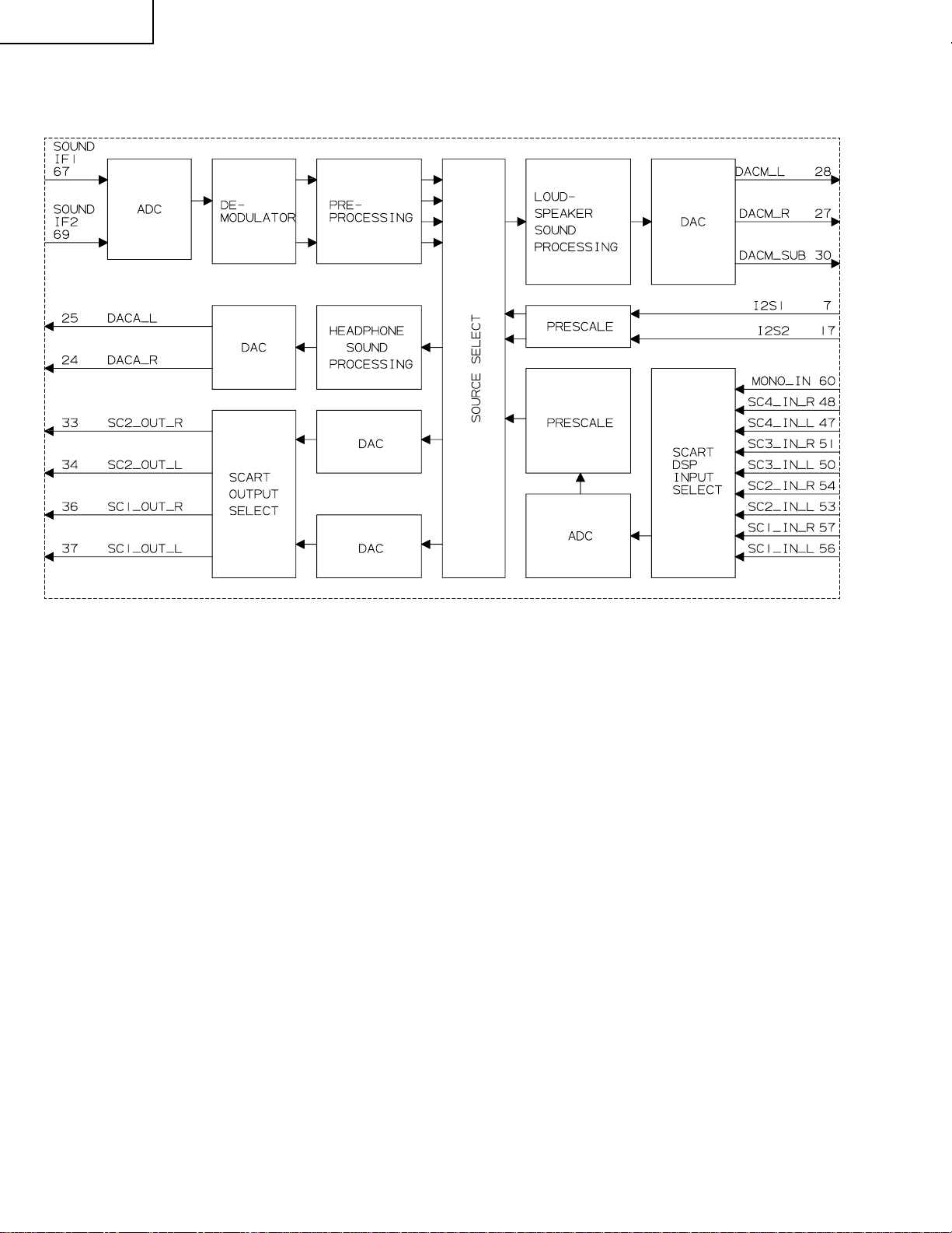
Ë RH-iX3371CEZZ (ASSY: IC2501)
» Multi Standard Sound Processor
» Block Diagram
28
Page 29
» Pin Function
Pin No. Pin Name I/O Pin Function
1
2
3
4
5
6
7
8
9
10
11, 12, 13
14, 15, 16
17
18, 19, 20
21
22, 23
24
25
26
27
28
29
30
31, 32
33
34
35
36
37
38
39
40
41, 42
43, 44
45
46
47
48
49
50
51
52
53
54
55
56
57
58
59
60
61, 62
63, 64
65, 66
67
68
69
70
71
72
73
74
75, 76
77
78
79
80
NC
I2C_CL
I2C_DA
I2S_CL
I2S_WS
I2S_DA_OUT
I2S_DA_IN1
ADR_DA
ADR_WS
ADR_CL
DVSUP
DVSS
I2S_DA_IN2
NC
RESETQ
NC
DACA_R
DACA_L
VREF2
DACM_R
DACM_L
NC
DACM_SUB
NC
SC2_OUT_R
SC2_OUT_L
VREF1
SC1_OUT_R
SC1_OUT_L
CAPL_A
AHVSUP
CAPL_M
NC
AHVSS
AGNDC
NC
SC4_IN_L
SC4_IN_R
ASG4
SC3_IN_L
SC3_IN_R
ASG2
SC2_IN_L
SC2_IN_R
ASG1
SC1_IN_L
SC1_IN_R
VREFTOP
NC
MONO_IN
AVSS
NC
AVSUP
ANA_IN1+
ANA_INANA_IN2+
TESTEN
XTAL_IN
XTAL_OUT
TP
AUD_CL_OUT
NC
D_CTR_I/O_1
D_CTR_I/O_0
ADR_SEL
STANDBYQ
—
I/O
I/O
I/O
I/O
—
—
—
—
—
—
—
—
—
—
—
—
—
—
—
—
—
—
—
—
—
—
—
—
—
I/O
I/O
Not connected
I2C clock
I2C data
I2S clock
O
I
O
O
O
I
I
O
O
O
O
O
O
O
O
O
I
I
I
I
I
I
I
I
I
I
I
I
I
I
O
O
I
I
I2S word strobe
I2S data output
I2S1 data input
ADR data output
ADR word strobe
ADR clock
Digital power supply 5V
Digital ground
I2S2-data input
Not connected
Power-on-reset
Not connected
Headphone out, right
Headphone out, left
Reference ground 2
Loudspeaker out, right
Loudspeaker out, left
Not connected
Subwoofer output
Not connected
SCART 2 output, right
SCART 2 output, left
Reference ground 1
SCART 1 output, right
SCART 1 output, left
Volume capacitor AUX
Analog power supply 8V
Volume capacitor MAIN
Not connected
Analog ground
Analog reference voltage
Not connected
SCART 4 input, left
SCART 4 input, right
Analog Shield Ground 4
SCART 3 input, left
SCART 3 input, right
Analog Shield Ground 2
SCART 2 input, left
SCART 2 input, right
Analog Shield Ground 1
SCART 1 input, left
SCART 1 input, right
Reference voltage IF A/D converter
Not connected
Mono input
Analog ground
Not connected
Analog power supply 5V
IF input 1
IF common(can be left vacant, only if IF input 1 is also not in use)
IF input 2(can be left vacant, only if IF input 1 is also not in use)
Test pin
Crystal oscillator
Test pin
Audio clock output (18.432MHz)
Not connected
D_CTR_I/O_1
D_CTR_I/O_0
I2C Bus address select
Stand-by (low-active)
PZ-43MR2E
PZ-50MR2E
29
Page 30
PZ-43MR2E
PZ-50MR2E
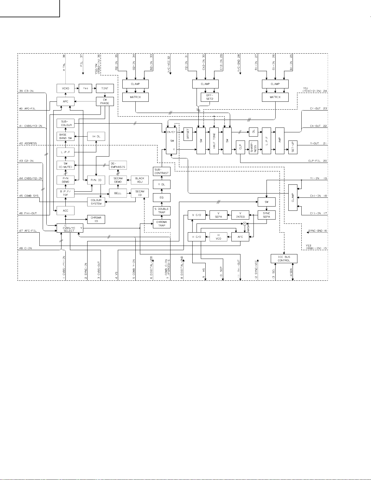
Ë VHiTB1274AF-1Q (ASSY: IC801, IC802)
» VIDEO/CHROMA Processor
» Block Diagram
30
Page 31

» Pin Function
Pin No. Pin Name I/O Pin Function
1
2
3
4
5
6
7
8
9
10
11
12
13
14
15
16
17
18
19
20
21
22
23
24
25
26
27
28
29
30
31
32
33
34
35
36
37
38
39
40
41
42
43
44
45
46
47
48
CVBS1/Y1-IN
SYNC-IN
CVBS-OUT
VS
COMB Y -IN
D-VDD
COMB C-IN
D-GND
HS
SCP
Yvi-IN
SYNC-VCC
SCL
SDA
YS3
(RGB1-in)
SYNC-GND
Cr1-IN
Cb1-IN
Y1-IN
CLP-FIL
Y-OUT
Cb-OUT
Cr-OUT
YS1
(YVbC2-IN)
B1-IN
G1-IN
R1-IN
Y/C-GND
Cr2-IN
Cb2-IN
Y2-IN
Y/C-VCC
B2-IN
G2-IN
R2-IN
YS2/YM
(RGB2-IN)
FIL.
X’TAL
C3-IN
APC-FIL
CVBS3/Y3-IN
ADDRESS
C2-IN
CVBS2/Y2-IN
COMB SYS
Fsc-OUT
AFC-FIL
C1-IN
I
I
O
O
I
—
I
—
O
O
O
—
I
I/O
I
—
I
I
I
—
O
O
O
I
I
I
I
—
I
I
I
—
I
I
I
I
—
—
I
—
I
I
I
I
O
O
—
I
CVBS1 or Y1-IN signal input.
Sync signal input.
CVBS or Y+C signal output terminal.
Counted-down vertical sync signal output.
Input of Y signal coming from comb filter. Open when not used.
DDS/BUS/V-CD/H-CD block power supply. DC5V (standard).
Input of C signal coming from comb filter. Open when not used.
DDS/BUS/V-CD/H-CD block grounding terminal.
H-AFC-processed horizontal sync signal output.
Sand Castle Pulse output. Clamping pulse and horizontal blanking pulse outputs.
Output of sync input Y signal selected with Video-SW.
SYNC/HVCO block power supply. DC5V (standard).
I2C BUS SCL terminal.
I2C BUS SDA terminal.
Selector switch for main signal and RGB1 input signal. YS3 input effective only when
“RGB1-ENB” is set at “enable” in bus setting.
SYNC/HVCO block grounding terminal.
Y1/Cb1/Cr1 signal input.
Y clamp filter to be connected.
Y/Cb/Cr signal output.
Selector switch for main signal and Y/Cr/Cb2 input signal.
RGB1 signal input. This input is selected at YS3 or I2C BUS.
Y/C/Text/Video-SW/1HDL block grounding terminal.
Y2/Cb2/Cr2 signal input. This input is selected at YS1.
Open when not used.
Y/C/Text/Video-SW/1HDL block power supply. DC5V (standard)
RGB2 signal input. This input is selected at YS2.
Open when not used.
Selector switch for main signal and RGB2 input signal.
Connected to Y/C-VCC terminal.
16.2MHz crystal oscillator to be connected.
Chroma signal input. Open when not used.
Chroma demodulation filter to be connected.
CVBS3 or Y3 signal input. Open when not used.
Slave address to be preset.
Chroma signal input. Open when not used.
CVBS2 or Y2 signal input. Open when not used.
Received color system judgment result to be output from this pin and pin 46.
Subcarrier output.
AFC detection filter to be connected.
Chroma signal input. Open when not used.
PZ-43MR2E
PZ-50MR2E
31
Page 32

PZ-43MR2E
PZ-50MR2E
Ë VHICXA2101Q-1 (ASSY: IC803)
» Baseband Video Signal Processor
» Block Diagram
» Pin Function
Pin No. Pin Name I/O Pin Function
1
2
3
4
5
6
7
8
9
10
11
12
13
14
15
16
17
IN2-H
IN2-V
IN2-1
IN2-2
IN2-3
Vcc-MAT
IN3-H
IN3-V
IN3-1
IN3-2
IN3-3
GND-MAT
IN4-H
IN4-V
IN4-1
IN4-2
IN4-3
I
I
I
I
I
—
I
I
I
I
I
—
I
I
I
I
I
IN2-H : Independent horizontal sync signal input terminal.
IN2-V : Independent vertical sync signal input terminal.
IN2 line signal input terminal.
Selector line and sync processor line power terminal.
IN3-H : Independent horizontal sync signal input terminal.
IN3-V : Independent vertical sync signal input terminal.
IN3 line signal input terminal.
Selector line and sync processor line grounding terminal.
IN4-H : Independent horizontal sync signal input terminal.
IN4-V : Independent vertical sync signal input terminal.
IN4 line signal input terminal.
32
Page 33

» Pin Function
Pin No. Pin Name I/O Pin Function
18
19
20
21
22
23
24
25
26
27
28
29
30
31
32
33
34
35
37
39
36
38
40
41
42
43
44
45
46
47
48
49
50
51
52
53
54
55
56
57
58
59
60
61
62
63
64
65
66
67
68
69
70
71
72
73
74
75
76
77
78
79
80
V-PH
IN5-H
IN5-V
IN5-1
IN5-2
IN5-3
H-PH
YG-OUT
YG-IN
IREF-SYNC
VS-OUT
HS-OUT
Vcc-OUT
SCP-IN
VTIM-IN
HP-IN
GND-OUT
R-OUT
G-OUT
B-OUT
R-SH
G-SH
B-SH
IK-IN
PABL-FIL
ABL-FIL
ABL-IN
YS/YM-1
LR1-IN
LG1-IN
LB1-IN
YS/YM-2
LR2-IN
LG2-IN
LB2-IN
ADDRESS
DPIC-C
SCL
SDA
DPIC-MUTE
CLP-C
VM-OUT
VM/SHP/COL-OFF
YCBCR-SW
ECR-IN
ECB-IN
EY -IN
V1-IN
H1-IN
CR1-IN
CB1-IN
Y1-IN
GND-SIG
IREF-YC
Vcc-SIG
SELCR-IN
SELCB-IN
SELY-IN
SELY-OUT
SELCB-OUT
SELCR-OUT
SELH-OUT
SELV-OUT
I
I
I
I
I
O
I
O
O
O
I
I
I
O
O
O
O
I
I
I
I
I
I
I
I
I
I
I
I
O
I
I
I
I
I
I
I
I
I
—
—
I
I
I
O
O
O
O
O
Vsync peak holding capacitor connection terminal.
IN5-H : Independent horizontal sync signal input terminal.
IN5-V : Independent vertical sync signal input terminal.
IN5 line signal input terminal.
Hsync peak holding capacitor connection terminal.
Sync separation composite video signal output terminal.
Sync separation composite video signal input terminal.
Reference current setting terminal (about 4.6V)
Used to select between IN1-line HV and IN2/IN5-line selector output HV by I2C BUS
“YCBCR/MAT” and feed out the signal in positive polarity.
RGB line power terminal.
Sand-Castle-Pulse input terminal.
V timing pulse input terminal.
H pulse input terminal.
RGB line grounding terminal.
RGB signal output terminal.
Output to be made at 2.6Vp-p with 100IRE white input.
RGB AKB sample-and-hold terminal.
Reference pulse to return to this terminal.
Peak ABL peak holding terminal.
Used to form LPF for ABL control signal.
ABL control signal input terminal.
YM1/YS1 control input terminal. Input level to be of 3 values.
VM turning-off function also available when YM and YS have reached their specified values.
Analog RGB1 signal input terminal.
YM2/YS2 control input terminal. Input level to be of 3 values.
VM turning-off function also available when YM and YS have reached their specified values.
Analog RGB2 signal input terminal.
I2C BUS slave address setting terminal.
Capacitor to be connected for grounding in order to detect the black signal in dynamic
picture (black stretching).
I2C BUS standard SCL (Serial Clock) input terminal.
I2C BUS standard SDA (Serial Data) input terminal.
Used to control MUTE of dynamic picture (black stretching).
Y line clamp capacitor connection terminal.
VM output terminal to feed out Y signal’s differential waveform in positive polarity.
Used to turn off VMÅASHARPNESS and COLOUR. Input level to be 3 values
Used to switch between INT and EXT SW input signals. External input terminal to be
selected at High level.
External Y, Cb, and Cr input terminals.
IN1-line HV input terminal. Positive-polarity input.
IN1-line Y, Cb, and Cr input terminals.
Y color difference signal processor grounding terminal.
Reference current setting terminal (mainly for Y color difference signal processing line).
Y color difference signal processor power terminal.
Used to feed in selector outputs Y, Cb, and Cr through clamp capacitor.
IN2- thru IN5-line selector output terminals.
Used to feed out Y-, Cb-, and Cr-converted signals.
IN2 thru IN5 selector HV output terminals.
PZ-43MR2E
PZ-50MR2E
33
Page 34

PZ-43MR2E
PZ-50MR2E
Ë RH-iX3566CEZZ (ASSY: IC1901)
» PLD (Programmable Logic Device)
» Pin Function
Pin No. Pin Name I/O Pin Function
1
2
3
4
5
6
7
8
9
10
11
12
13
14
15
16
17
18
19
20
21
22
23
24
25
26
27
28
29
30
31
32
33
34
35
36
37
38
39
40
41
42
43
44
TDI
VD1
SP_HD
GND
SP_VD
SP_CP
TMS
HD3
VCC
VD3
GND
MODEA
MODEB
MODEC
SELA
GND
VCC
SELO
HD2
VD2
HDS
VDS
US_VD
GND
US_HD
TCK
TEXT_VD
TEXT_HD
VCC
GND
PL_BLK
TDO
PLCP
PL_HD
PL_VD
GND
GCLK1
OE1
GCLRn
OE2/GCLK2
VCC
CNR_CP
CNR_HBLK
HD1
I/O
I/O
I/O
—
I/O
I/O
I/O
I/O
—
I/O
—
I/O
I/O
I/O
I/O
—
—
I/O
I/O
I/O
I/O
I/O
I/O
—
I/O
I/O
I/O
I/O
—
—
I/O
I/O
I/O
I/O
I/O
—
—
I/O
I/O
I/O
Ground
Power supply (3.3V)
Ground
Ground
Power supply (3.3V)
Ground
Power supply (3.3V)
Ground
I
I
I
I
Ground
External clock input. 16MHz
Power supply (3.3V)
34
Page 35

Ë VHiTA1318AF-1 (ASSY: IC604)
» Sync Processor
» Block Diagram
PZ-43MR2E
PZ-50MR2E
35
Page 36

PZ-43MR2E
PZ-50MR2E
» Pin Function
Pin No. Pin Name I/O Pin Function
3
1
11
4
2
10
5
6
7
8
20
9
24
12
13
15
14
16
17
18
21
19
22
23
HD1-IN
HD2-IN
HD3-IN
VD1-IN
VD2-IN
VD3-IN
ANALOG GND
AFC FILTER
HVCO
VCC
DAC1
(V . SYNC output)
DAC2
(H/C. SYNC output)
DAC3
CP-OUT
HD1-OUT
HD2-OUT
DIGITAL GND
SDA
SCL
ADDRESS SW
SYNC1-IN
SYNC2-IN
VD1-OUT
VD2-OUT
—
—
—
—
O
O
O
O
O
O
—
I/O
O
O
I
I
I
I
I
I
I
I
I
I
Input the horizontal synchronizing signal.
It’s polarity corresponds to both positive and negative.
Input from this pin does not be synchronized internally.
Input the horizontal vertical signal.
It’s polarity corresponds to both positive and negative.
Input from this pin does not be synchronized internally.
The GND pin for analog circuit block.
Connect the filter for horizontal AFC. The frequency of the horizontal output is varied
by the volyage at this pin.
Connect the ceramic oscillator for horizontal oscillator.
The VCC pin. (9.0V)
DAC1 output pin. When TEST mode, VD or vertical sync signal to frequency counter
circuit is output.
DAC2 output pin. When TEST mode, HD or composite sync signal to frequency
counter circuit is output.
DAC3 output pin. This pin is open-collector system. When TEST mode, test pilses for
the shipping is output.
Clamp pulse output pin. CP mode at synchronization circuit is output.
HD output pin. This pin is open-collector system.
HD1/HD2 does not be synchronizing and they are output from this pin.
It’s polarity is switched by BUS write function.
The GND pin for logic circuit block.
The SDA pin for I2C BUS.
The SCL pin for I2C BUS.
Slave address switch.
Input a signal to separate sync signal.
VD output pin. This pin is open-collector system.
VD1/VD2 does not be synchronizing and they are output from this pin.
It’s polarity is switched by BUS write function.
36
Page 37

Ë VHiCXD2064Q-1 (ASSY: IC402, IC405)
» Digital Comb Filter
» Block Diagram
PZ-43MR2E
PZ-50MR2E
37
Page 38

PZ-43MR2E
PZ-50MR2E
» Pin Function
Pin No. Pin Name I/O Pin Function
1
2
3
4
5
6
7
8
9
10
11
12
13
14
15, 28, 32, 33, 35,
16, 27, 34
18, 29, 36
17
19
20
21
22
23
24
25
26
30
31
37
38
39
40
41
42
43
44
45
46
47
48
CLPO
ADIN
RB
ADVS
ADVD
RT
ACO
DAVD
AYO
DAVS
VG
VRF
IRF
VB
TEST
DVDD
DVSS
MOD2
MOD1
VEH3
VEH2
VEH1
PNR
DTR
NTPL2
NTPL1
APCN
TRAP
FIN
CKSL
PLSL
MCKO
ADCK
CPO
PLVS
VCV
PLVD
CLVD
CLPEN
CLVS
O
I
O
—
—
O
O
—
O
—
O
I
O
O
I
—
—
I
I
I
I
I
I
I
I
I
I
I
I
I
I
O
I
O
—
I
—
—
I
—
Built-in clamp circuit current output terminal. To be connected to ADIN when built-in
clamp is used.
Comb filter analog input (A/D converter) terminal.
A/D converter reference bottom voltage. (standard 0.52V)
A/D converter analog grounding terminal.
A/D converter analog power terminal. (5.0V)
A/D converter reference top voltage. (standard 2.6V)
Analog chroma signal output terminal. Resistance to be added between this pin and
GND for obtaining the output.
D/A converter analog power terminal. (5.0V)
Analog luminance signal output terminal. Resistance to be added between this pin and
GND for obtaining the output.
D/A converter analog grounding terminal.
D/A converter terminal.
Y,C ch D/A converter output full-scale setting terminal.
x16 resistance to be connected against D/A converter output resistance “R”.
D/A converter terminal.
Test terminal. (fixed at Low)
Digital power terminal. (5.0V)
Digital grounding terminal.
Y/C separation mode setting terminal.
MODE2 MOD1
L L Most suitable process mode
H L BPF separation mode
Vertical contour enhancement setting terminal.
L: NTSC H: P AL, M-PAL, N-PAL
Fixed at Low.
NTSC/P AL/M-PAL/N-PAL mode setting terminal.
NTPL2 NTPL1
L L NTSC
HHPAL
H L M-PAL
H H N-PAL
Horizontal aperture correction circuit setting terminal. L: off, H: on
Trap filter circuit setting terminal. L: off, H: on
Clock input terminal.
PLL control terminal. VCO oscillator output’s 4fsc clock to be fed in.
FIN input fsc to be selected.
Clock (4fsc) output terminal.
A/D converter clock input terminal. To be connected to MCKO.
PLL phase comparator output terminal.
PLL analog grounding terminal.
VCO control voltage input terminal.
PLL analog power terminal. (5.0V)
Clamp D/A converter analog power terminal. (5.0V)
Clamp circuit enable terminal.
Clamp D/A converter analog grounding terminal.
38
Page 39

Ë VHiML6428C1-1 (ASSY: IC404, IC407)
» Low Pass Video Filter IC
» Block Diagram
PZ-43MR2E
PZ-50MR2E
» Pin Function
Pin No. Pin Name I/O Pin Function
1
2
3
4
5
6
7
8
YIN
VCC
GND
CIN
YOUT
VCCO
CVOUT
COUT
I
—
—
I
O
—
O
O
Luminance input
5V supply for filters and references.
Ground
Chrominance input
Chrominance output
Composite video output
5V supply for output stages
Luminance output
39
Page 40

PZ-43MR2E
PZ-50MR2E
Ë RH-iX3473CEZZ (ASSY: IC804, 810)
Ë RH-iX3474CEZZ (ASSY: IC811)
» Monolithic Video Filter
* RH-iX3473CEZZ is 6.7MHz at Cut-off frequency.
* RH-iX3474CEZZ is 30MHz at Cut-off frequency.
» Block Diagram
» Pin Function
Pin No. Pin Name I/O Pin Function
1
2
3
4
5
6
7
8
9
10
11
12
13
14
15
16
A/B MUX
RINA/YINA
GND
VCC
RINB/YINB
GINA/UINA
GINB/UINB
BINA/VINA
BINB/VINB
BOUT
GOUT
VCCO
ROUT
GNDO
DISABLE
SYNC IN
—
I
—
—
I
I
I
I
I
O
O
—
O
—
I
I
Logic input pin to select between Bank <A> and Bank <B> video inputs.
This pin is internally pulled high.
Unfiltered analog R- or Y-channel input for Bank <A>, Sync must be provided at SYNC
IN pin.
Analog ground.
Analog 5V supply.
Unfiltered analog R or Y-channel input for Bank <B>, Sync must be provided at SYNC
IN pin.
Unfiltered analog G or U-channel input for Bank <A>, Sync must be provided at SYNC
IN pin.
Unfiltered analog G or U-channel input for Bank <B>, Sync must be provided at SYNC
IN pin.
Unfiltered analog B or V-channel input for Bank <A>, Sync must be provided at SYNC
IN pin.
Unfiltered analog B or V-channel input for Bank <B>, Sync must be provided at SYNC
IN pin.
Analog B or V-channel output.
Analog G or U-channel output.
5V power supply for output buffers.
Analog R or Y-channel output.
Analog ground.
Disable/Enable pin. Turns the chip off when logic high. Internally pulled low.
Input for an external H-sync logic signal for filter channels. CMOS level input. Active
High.
40
Page 41

Ë VHiFA3675F/-1 (ASSY: IC1702)
» 6-channel DC-DC Converter IC
» Block Diagram
PZ-43MR2E
PZ-50MR2E
41
Page 42

PZ-43MR2E
PZ-50MR2E
» Pin Function
Pin No. Pin Name I/O Pin Function
1
2
3
4
5
6
7
8
9
10
11
12
13
14
15
16
17
18
19
20
21
22
23
24
25
26
27
28
29
30
31
32
33
34
35
36
37
38
39
40
41
42
43
44
45
46
47
48
VCC1
RT
CT
CS3
CS5
CS4
CS1
CS2
VREF
CREF
VREG
IN2FB2
IN1FB1
IN5+
IN5FB5
IN6FB6
IN3+
IN3FB3
IN4+
IN4FB4
CP
GND
TLSEL
CNT5
CNT4
CNT2
CNT3
CNT1
VCC2
VDRV
PGND1
OUT1S
OUT1
OUT4
OUT3
OUT2S
OUT2
OUT6S
OUT6
OUT5
OUT5S
PGND2
—
—
—
—
—
—
—
—
O
O
O
I
O
I
O
I
I
O
I
O
I
I
O
I
I
O
I
—
I
I
I
I
I
I
—
O
—
O
O
O
O
O
O
O
O
O
O
—
Power supply for control circuit.
Oscillator timing resistor.
Oscillator timing capacitor.
Soft start for Ch.3 & Ch.4.
Soft start for Ch.6.
Soft start for Ch.5.
Soft start for Ch.1
Soft start for Ch.2.
Reference voltage output.
Capacitor for reference voltage output.
Regulated for voltage output.
Ch.2 inverting input to error amplifier.
Ch.2 output of error amplifier.
Ch.1 inverting input to error amplifier.
Ch.1 output of error amplifier.
Ch.5 non-inverting input to error amplifier.
Ch.5 inverting input to error amplifier.
Ch.5 output of error amplifier.
Ch.6 inverting input to error amplifier.
Ch.6 output of error amplifier.
Ch.3 non-inverting input to error amplifier.
Ch.3 inverting input to error amplifier.
Ch.3 output of error amplifier.
Ch.4 non-inverting input to error amplifier.
Ch.4 inverting input to error amplifier.
Ch.4 output of error amplifier.
Timing capacitor for timer latch delay.
Ground.
Ch.3 & Ch.4 timer latch selection(Low:disable).
Ch.6 ON/OFF function.
Ch.5 ON/OFF function.
Ch.2 ON/OFF function.
Ch.3 & Ch.4 ON/OFF function.
Ch.1 ON/OFF function.
Power supply for output stage.
Bias for logic circuit of output.
Power ground.
Ch.1 source electrode of output stage.
Ch.1 output(for Pch-MOSFET)
Ch.4 output(for Pch-MOSFET)
Ch.3 output(for Pch-MOSFET)
Ch.2 source electrode of output stage.
Ch.2 output(for Pch-MOSFET)
Ch.6 source electrode of output stage.
Ch.6 output(for Pch-MOSFET)
Ch.5 output(for Pch-MOSFET)
Ch.5 source electrode of output stage.
Power ground.
42
Page 43

Power-on failure (Front LED indicator stays off.)
NO
YES
Is the power cable
connector properly
connected with the set?
Reinsert the power cable
connector and turn on the
power again.
NO
YES
Are F701 and F702 intact
in place?
Replace F701 or F702 and
turn on the power again. If
the fuse blows out again,
replace VA701, Q701, Q703
and IC702 and check the
performance again.
NO
YES
Does the BACK5V line
function?
Check the BACK5V line. Is
there any defective part or
short-circuit?
Check the set's wire
harnesses, FFCs and other
parts for their connections.
YES
Repair the defective
part or short-circuit.
Check the
performance again.
NO
Check IC702,
T702, PC703 and
their peripheral
circuits.
Power switch on, but no power
(Front LED indicator does not change from red to green, but remains in red.)
NO
YES
Are the MDR and DVI cable connectors (white
and gray) properly connected with the PDP
and the set as well?
NO
YES
YES
YES
Is the impedance of the M+10V line
as specified? (Measure the resistance
between F1702 and GND.)
NO
NO
YES
Are there voltage
fluctuations along the OVP
line (pin (12) of P1502)?
NO
Check the M+10V line as well
as its circuit parts.
YES
Are the DC/DC converter output
lines and MOS-FET (Q1712,
Q1716, Q1726 and Q1718) as
specified?
NO
Chekc the D_POW and
B+2.5V_POW lines (pins (6)
and (7) of IC1503).
YES
NO
Check the DC/DC converter output
lines and replace the MOS-FET
(Q1712, Q1716, Q1726 and Q1718).
NO
YES
Is the PS_ON terminal (pin (1) of CN703) at HI
(3.5V)?
Check the internal parts of the power
unit (Q703, Q704, Q708, Q709, D717,
D710 and D711).
Are the D_POW and B+2.5V_POW
settings (pins (30), (32), (33) and (34)
of IC1701) at HI?
NO
YES
Do the +5V line (pin (10) of P1703),
+2.5V line (pins (5) and (6) of P1702),
and +3.3V line (pin (8) of P1702) all
function?
Check the set's wire harnesses,
FFCs and other parts for their
connections.
Replace IC1701.
Check the PS_ON line.
Is the M+10V line as specified?
Is the PDP's power switch on?
Reinsert the connectors, and turn on the
power again.
Turn on the PDP's power switch.
Æ
POWER Unit
TROUBLE SHOOTING TABLE
PZ-43MR2E
PZ-50MR2E
43
Page 44

PZ-43MR2E
No sound
No sound from speaker
NO
YES
YES
Does output icon denote speaker when
operating audio volume control?
NO
NO
Does output icon denote lineout when
operating audio volume control?
Monitor output in the main menu is set
to "Variable". Switch it to "Fixed".
YES
Is audio output available at each related
pin of IC2501 (MULTI SOUND
PROCESSOR) normal?
Pins (36) and (37) of IC2501 (SC1 OUT
L/R)
YES
Check Q2505 and 2504 (Buffer) and
its peripheral circuits
YES
Check PC I/F Unit and its peripheral
circuits.
No audio output (SCART1)
YES
Is audio output available at each
related pin of IC2501 (MULTI SOUND
PROCESSOR) normal?
Pins (27) and (28) of IC2501
(SC1 OUT L/R)
YES
Check the circuit between pins (27) and
(28) of IC2501 and pins (3) and (1) of
SCART1, as well as audio mute circuit.
NO
Is tuner audio input available at each
related pin of IC2501
(MULTI SOUND PROCESSOR) normal ?
Pin (67) of IC2501 (SOUND IF1)
Pin (69) of IC2501 (SOUND IF2)
NO
NO
NO
Is audio output available at each related pin of
IC1301 (AV SWITCH) normal?
Pins (52) and (54) of IC1301 (L/R OUT1)
Pins (43) and (45) of IC1301 (L/R OUT2)
Pins (38) and (40) of IC1301 (L/R OUT3)
NO
No audio output (SCART2/3)
YES
Is audio output available at each
related pin of IC2501 (MULTI SOUND
PROCESSOR) normal?
Pins (27) and (28) of IC2501
(SC1 OUT L/R)
YES
Check the circuit between pins (27) and
(28) of IC2501 and pins (3) and (1) of
SCART2/3, as well as audio mute circuit.
No monitor audio output
YES
Is normal audio output available at
each related pin of IC2501
(MULTI SOUND PROCESSOR)?
Pins (34) and (33) of IC2501
(SC2 OUT L/R)
YES
Check the circuit between pins (34) and
(33) of IC2501 and J1101 (monitor audio
output), as well as audio mute circuit.
Check the plasma display section.
On TV reception
On external input / PC input
Check IC2501 (MULTI SOUND PROCESSOR) and its peripheral circuits.
Check B.P.F. of SIF1 and SIF2 respectively.
Check TU1101 (U/V tuner) and peripherals.
Is each audio input circuit of IC1301 (AV SWITCH)
normal?
Between SCART1 Pins (6), (2) and IC1301 Pins (2), (4)
Between SCART2 Pins (6), (2) and IC1301 Pins (9), (11)
Between SCART3 Pins (6), (2) and IC1301 Pins (16), (18)
Between front input (J3401) and IC1301 Pins (23), (25)
Between PC input (J3403) and IC1301 Pins (29), (31)
Check IC1301 (AV SWITCH) and peripherals.
PZ-50MR2E
TROUBLE SHOOTING TABLE (Continued)
44
Page 45

No Picture (1)
YES
NO
YES
No external input <SCART1 AV>
Check the line between
pin (20) of SCART1 and
pin (3) of IC1301.
YES
YES
No external input <SCART2 AV>
Check the line between
pin (20) of SCART2 and
pin (10) of IC1301.
YES
NO
YES
No external input <SCART3 AV>
NO
Check IC1301 and its
peripheral circuits.
Is there AV signal input
at pin (17) of IC1301 (AV
SWITCH)?
Is there AV signal input
at pin (10) of IC1301 (AV
SWITCH)?
Is there AV signal input
at pin (3) of IC1301 (AV
SWITCH)?
YES
Are there MAIN-R/G/B signal inputs at pins (5), (7)
and (9) of IC811 (30MHz L.P.F.), respectively?
YES
NO
Check IC811 and
its peripheral
circuits.
YES
YES
YES
NO
Check IC810 and
its peripheral
circuits.
Are there SUB-R/G/B signal outputs
at pins (13), (11) and (10) of IC810,
respectively? (in STD mode)
Are there SUB-R/G/B signal outputs
at pins (13), (11) and (10) of IC811,
respectively? (in HDTV mode)
Check the line between
pin (20) of SCART3 and
pin (17) of IC1301.
YES
NO
Check the line between
IC405 and IC801.
YES
Are there MAIN-Y signal inputs at pins (1) and (44) of IC801
(MAIN VIDEO CHROMA) as well as MAIN-C signal inputs at pins
(43) and (48)(composite signal at pin (1) in SECAM system)?
NO
Check the line between
IC402 and IC802.
Are there SUB-Y signal input at pin (44) of IC802 (SUB
VIDEO CHROMA) (at pin (1) in NTSC system) as well as
SUB-C signal input at pin (43) (at pin (48) in NTSC system)?
YES
NO
Check IC801 and its
peripheral circuits.
YES
Are there MAIN-Y/Cb/Cr signal outputs at pins (21),
(22) and (23) of IC801, respectively?
NO
Check IC802 and its
peripheral circuits.
Are there SUB-Y/Cb/Cr signal outputs at pins (21),
(22) and (23) of IC802, respectively?
YES
NO
Check the line between
IC801 and IC803.
YES
Are there MAIN-Y/Cb/Cr signal inputs at pins (69), (68)
and (67) of IC803 (RGB DECODER), respectively?
NO
Check the line between
IC802 and IC804.
Are there
SUB-Y/Cb/Cr
signal inputs at pins (5), (9)
and (7) of IC804 (6.7MHz L.P.F.), respectively?
YES
NO
Check IC803 and its
peripheral circuits.
YES
YES
Are there MAIN-R/G/B signal outputs at pins (35),
(37) and (39) of IC803, respectively?
NO
Check IC804 and its
peripheral circuits.
Are there SUB-R/G/B signal outputs at pins (13),
(11) and (10) of IC804, respectively?
NO
NO
NO
Select INPUT1 AV on
the menu screen.
Select INPUT2 AV on
the menu screen.
NO
Is INPUT3 AV selected
on the Input Select
menu screen?
Is INPUT2 AV selected
on the Input Select
menu screen?
Is INPUT1 AV selected
on the Input Select
menu screen?
Select INPUT3 AV on
the menu screen.
Are there MAIN and SUB video signal outputs at pins (56) and (44) of IC1301, respectively?
YES
NO
Check the lines between
IC1301, IC405 and
IC402.
Are there video signal inputs at pins (1) and (2) of IC405 (MAIN COMB FILTER) and IC402 (SUB COMB FILTER)?
Check the PC I/F unit.
<MAIN system> <SUB system>
<HDTV mode> <STD mode>
Are there MAIN-R/G/B signal inputs at pins (5), (7)
and (9) of IC810 (6.7MHz L.P.F.), respectively?
C
A
D
F
B
E
TROUBLE SHOOTING TABLE (Continued)
PZ-43MR2E
PZ-50MR2E
45
Page 46

PZ-43MR2E
No picture (2)
NO
YES
NO
YES
No external input picture (SCART2 Y/C)
Is INPUT2 Y/C selected on
Input Select menu screen?
Select INPUT2 Y/C on
menu selection screen.
Is Y signal input available at
pin (10) and C signal input
at pin (12) of IC1301 (AV
SWITCH) respectively?
Check the circuit between
pins (20) and (25) of
SCART2 and pins (10) and
(12) of IC1301.
Check the circuit between
pins (20) and (15) of
SCART3 and pins (17) and
(19) of IC1301.
Check the circuit
between pin (23) of
TUNER and pin (63) of
IC1301.
NO
YES
NO
YES
NO
No external input picture (SCART3 Y/C)
Is INPUT3 Y/C selected on
Input Select menu screen?
Select INPUT3 Y/C on
menu selection screen.
Is Y signal input available at
Pin (17) and C signal input
at pin (19) of IC1301 (AV
SWITCH), respectively?
Check IC1301 and
peripheral circuits.
NO
YES
NO
YES
No TV picture
Is video output available at pin
(23) of TU1101 (U/V tuner)?
Check TUNER and its
peripheral circuit.
Is video input signal
available at pin (63) of
IC1301 (AV SWITCH)?
No picture (3)
NO
YES
NO
YES
No external input picture (SCART1 RGB)
Is INPUT1 RGB selected
on Input Select menu
screen?
Select INPUT1 RGB on
menu selection screen.
Is RGB signal input
available at pins (59),
(61) and (63) of IC1401
(AV SWITCH)?
Check the circuit
between pins (15), (11)
and (7) SCART and pins
(59), (61) and (63).
NO
YES
NO
YES
No external input picture (SCART3 RGB)
Is INPUT3 RGB selected
on Input Select menu
screen?
Select INPUT3 RGB on
menu selection screen.
Is RGB signal input
available at pins (5), (7)
and (9) of IC1401 (AV
SWITCH)?
Check the circuit between
pins (15), (11) and (7) of
SCART3 and pins (5), (7)
and (9) of IC1401.
NO
YES
NO
YES
No component picture
Is INPUT3 COMPONENT
selected on Input Select
menu screen?
Select INPUT3
COMPONENT on menu
selection screen.
Is component signal input
available at pins (15), (17)
and (19) of IC1401 (AV
SWITCH)?
Check the circuit between
J1101 (component signal
input terminal) and
IC1401 pins (15), (17)
and (19) of IC1401.
NO
YES
Is RGB signal output
available at pins (50), (48)
and (46) of IC1401?
Check IC1401 and
peripheral circuits.
NO
YES
Is RGB signal output
available at pins (50), (48)
and (46) of IC1401?
Check IC1401 and
peripheral circuits.
NO
YES
YES
YES
YES
Is component signal output
available at pins (38), (36)
and (34) of IC1401?
Check IC1401 and
peripheral circuits.
NO
Is RGB signal input available
at pins (27), (26) and (25) of
IC801 (MAIN VIDEO
CHROMA) respectively?
Check the circuit between
pins (5), (48) and (46) of
IC1401 and pins (27),
(26) and (25) of IC1801.
NO
Is RGB signal input available
at Pins (27), (26) and (25) of
IC802 (SUB VIDEO
CHROMA) respectively?
Check the circuit between
pins (50), (48) and (46) of
IC1401 andpins (27), (26)
and (25) of IC802.
NO
Is component signal input
available at pins (3), (4)
and (5) of IC803 (RGB
DECODER) respectively?
Check the circuit between
pins (38), (36) and (34) of
IC1401and pins (3), (4)
and (5) of IC803.
C
A
B
Is MAIN-Y signal output available at pin (56) and MAIN-C signal output at pin (58) of IC1301, respectively?
Is SUB-Y signal output available at pin (44) and SUB-C signal output at pin (47) of IC1301, respectively?
DEF
PZ-50MR2E
TROUBLE SHOOTING TABLE (Continued)
46
Page 47

No picture (4)
NO
YES
Is INPUT4
selected in Input
Source?
Select INPUT4
in Input Source.
NO
YES
Is INPUT4
selected in Input
Source?
Select INPUT4
in Input Source.
NO
YES
Is video signal
input available at
pin (22) of IC1301
(AV SWITCH)?
Check the circuit
between J3401
(front INPUT4) AV
terminal and pin
(22) of IC1301.
NO
YES
Is Y signal input
available at pin (24)
and C signal input at
pin (26) of IC1301
(AV SWITCH)
respectively?
Check the circuit
between pins (2)
and (1) and pins
(24) and (26) of
IC1301.
NO
Is MAIN-Y signal output
available at pin (56)
and MAIN-C signal
output at pin (58) of
IC1301 respectively?
Is SUB-Y signal output
available at pin (44) and
SUB-C signal output at
pin (47) of IC1301
respectively?
Check IC1301
and peripheral
circuits.
No external input picture (INPUT4 AV) No external input picture (INPUT4 S-IN)
No picture (5)
NO
Is video signal
output available at
pin (41) of IC1301
(AV SWITCH)?
NO
Is Y signal output
available at pin (39)
and C signal output
at pin (37) of IC1301
(AV SWITCH)
respectively?
YES
YES
YES
Check the circuit
between pin (41) and
of IC1401 J1101
(monitor video output
terminal).
Check the circuit
between pins (39)
and (37) of IC1301
and pins (3), (4) of
J1102 (monitor S-
OUT terminal).
Confirm
input signal
is S-INPUT.
No monitor picture (AV) No monitor picture (S-OUT)
Check
IC1301 and
peripheral
circuits.
C
A
B
Check
IC1301 and
peripheral
circuits.
TROUBLE SHOOTING TABLE (Continued)
PZ-43MR2E
PZ-50MR2E
47
Page 48

PZ-43MR2E
Synchronization failure
NO
YES
Is VDM/HDM output
available at pins (28)
and (29) of IC803
(RGB DECODER)?
Check IC803 and
peripheral circuits.
NO
NO
YES
Is HI/VI input available
at pins (66)/(1) and
(65)/(2) of IC803?
Check the circuit
between pins (34)
and (35) of IC1901
and pins (66)/(1) and
(65)/(2) of IC803.
NO
YES
Is PL-HD/VD output
available at pins (34) and
(35) of IC1901 (PLD)?
Check IC1901 and
peripheral circuits.
YES
MAIN: Is HD1/VD1 input available at pins (44) and (2) of IC1901?
SUB: Is HD2/VD2 input available at pins (19) and (20) of IC1901?
COMPONENT: Is SP HD/VD input available at pins (40) and (5) of IC1901?
NO
Is HD1/VD1 output available
at pins (9) and (4) of IC801
(MAIN VIDEO CHROMA)?
Check IC801 and peripheral
circuits.
YES
NO
Is SP HD/VD output
available at pins (16) and
(28) of IC604 (SYNC SEP)?
Check IC604 and peripheral
circuits.
YES
NO
Is HD2M/VD2 output available
at pins (9) and (4) of IC802
(SUB VIDEO CHROMA)?
YES
Is video signal input
available at pin (21) of
IC1601 (TELETEXT CPU)?
Is TELETEXT compatible broadcast received (or are signals from other TELETEXT compatible
equipment received at video input terminal), and is TELETEXT selected on remote controller?
Check the circuit between
pin (56) of IC1301 and pin
(21) of IC1601.
NO
YES
Is signal input available at pins
(57), (58) and (59) of IC1601?
Check IC1601 and its
peripheral circuits.
NO
Is signal input available at
pins (57), (53) and (55) of
IC1301 (AV SWITCH)?
Check the circuit between
pins (57), (58) and (59) of
IC1601 and pins (57), (53)
and (55) of IC1301.
YES
NO
Select TELETEXT in
accordance with the
specified procedure.
Check IC802 and peripheral
circuits.
No TELETEXT screen
NO
YES
Is HDS/VDS output
available at pins
(21) and (22) of
IC1901 (PLD)?
Check IC1901
and peripheral
circuits.
NO
MAIN
SUB
Check the
circuit between
pins (9) and (4)
of IC801 and
pins (19) and
(20) of IC1901.
PZ-50MR2E
48
Page 49

No picture
NO
YES
No TV, video and component picture
Is input available at pins
(124), (133) and (139) of
IC4 normal?
Check CN6 and its
peripheral circuits.
NO
YES
Are TL207, TL208 and
TL211 normal?
Check CN6 and its
peripheral circuits.
NO
YES
Is digital output section
of IC4 normal?
Check IC4 and its
peripheral circuits.
NO
YES
Is digital output section
of IC310 normal?
Check IC310 and its
peripheral circuits.
NO
YES
Is digital output of IC25
normal?
Check IC25 and its
peripheral circuits.
No PC picture
YES
Is signal available at pins (21), (22), (24), (25), (27), (28), (30)
and (31) of IC413? (The signal is of high frequency (a little
less than 1GHz). Pay due attention to it during observation.)
Monitor problem is likely.
NO
PC I/F Unit (CPCi-
0056CE) internal problem
is likely.
No MAIN picture on single screen and dual screen.
No SUB picture on dual screen
NO
YES
Is input available at pins
(126), (136) and (141) of
IC4 normal?
Check CN8 and its
peripheral circuits.
NO
YES
Is digital output section
of IC4 normal?
Check IC4 and its
peripheral circuits.
NO
YES
Is digital output of IC25
normal?
Check IC25 and its
peripheral circuits.
TROUBLE SHOOTING TABLE FOR PC I/F UNIT
PZ-43MR2E
PZ-50MR2E
49
Page 50

PZ-43MR2E
L
CONTROL
C
CIRCUIT
CIRCUIT
PZ-50MR2E
PRINTED WIRING BOARD BLOCK DIAGRAM-1/2
»
PC I/F Unit
H
POWERREG.
PCR,G,BINPUT
CIRCUIT
G
VIDEOINA/D
CONVERTER
CIRCUIT
F
CN9
CONNECTOR
CN8
CONNECTOR
IC7
REG.
VIDEOMAIN/P
IC310
A/DCONV
IC8
REG.
IC4
A/DCONV
IC320
SDRAM
IC1
CPU
IC25
CIVIC
IC319
SDRAM
VIDEOPROCESSOR
CPCI-0056CE■
IC413
PANELLINK
IC405
RS-323RECIVER
CN3
DISPLAYOUT-1
CN5
RS-232C
PANELLINK
OUTPUT
CIRCUIT
RS-232CLINE
DRIVERI/F
CIRCUIT
E
»
D
C
COMP.AVSWITCH
CIRCUIT
B
AV Unit
IC1401
AVSWITCH
CN6
CONNECTOR
SC1101
SCART-1TERMINAL
ANALOGAVSWITCH
CIRCUIT
P1301
CONNECTOR
SC1401
CONNECTOR
CN7
CONNECTOR
SC1102
SCART-2/3TERMINAL
IC1301
AVSWITCH
CPUCIRCUIT
SC1402
CONNECTOR
COMPIN/MONI-OUTTERMINA
IC1102
J1101
FLASHMEMORY
IC1602
IC1601
TELTEXT
CN1
CONNECTOR
J1102
MONITORS-OUT
IC1603
P2502
CONNECTOR
IC2501
MULTISOUND
U/VTUNER
TELTEXT&AVLINK
CIRCUIT
P2503
CONNECTOR
A
P2501
CONNECTOR
654321
50
Page 51

PRINTED WIRING BOARD BLOCK DIAGRAM-2/2
»
MAIN Unit
H
PZ-43MR2E
PZ-50MR2E
SC1502
CONNECTOR
IC802
SUBVIDEO
CHROMA
G
SC1501
CONNECTOR
IC901
PLD
F
IC803
P901
ADJUSTING
CONNECTOR
RGBDECODER
IC403
CONTROL
SC1503
CONNECTOR
IC402
SUBCOMBFIL.
IC604
SYNCSEP.
IC801
MAINVIDEO
CHROMA
MAINCOMBFIL.
IC406
CONTROL
IC405
SC1504
CONNECTOR
IC1502
DAC
P1702
CONNECTOR
P1703
CONNECTOR
E
P1502
CONNECTOR
POWERSUPPLY
DC/DCCONVERTER
CIRCUIT
D
C
B
A
654321
51
Page 52

PZ-43MR2E
PZ-50MR2E
SYSTEM BLOCK DIAGRAM
H
G
F
E
D
C
B
A
87109654321
52
Page 53

PZ-43MR2E
PZ-50MR2E
53
1716 1918151413121110
Page 54

PZ-43MR2E
PZ-50MR2E
SIGNAL FLOW BLOCK DIAGRAM
H
G
F
E
D
C
B
A
87109654321
54
Page 55

PZ-43MR2E
PZ-50MR2E
55
1716 1918151413121110
Page 56

PZ-43MR2E
PZ-50MR2E
DC/DC CONVERTER BLOCK DIAGRAM
H
G
F
E
D
C
B
A
87109654321
56
Page 57

PZ-43MR2E
PZ-50MR2E
57
1716 1918151413121110
Page 58

PZ-43MR2E
PZ-50MR2E
POWER BLOCK DIAGRAM
H
G
F
E
D
C
B
A
87109654321
58
Page 59

PZ-43MR2E
PZ-50MR2E
59
1716 1918151413121110
Page 60

PZ-43MR2E
z
E
T
I
D
F
F
M
8
R
D
D
D
D
PZ-50MR2E
PC I/F BLOCK DIAGRAM
X6
25.175MHz
X5
79.794MHz
8
8
8
LCLK(79.79 4MH
DO_HS YNC
DO_VS YNC
DO_HD ISP
-C1_I NT
CKIO(24MHz)
-CS2
-WAIT_C1
-RESET_C1
-
RST_PLL
CPU BUS
WP
TX
RX
TX
RX
2
LH2
D
MS
H
CPCI-00 56CE
X4
CLR_ SW
12
HV SEL
1B
2B
4B
1A
2A
4A
-A /+B
RIN2
GIN2
BIN2
RIN1
GIN1
BIN1
ROUT
GOUT
BOUT
74LCX157
1Y
2Y
V0
4Y
Sync
Sel
IC411
12V->5VReg
IC7 PQ05TZ11
V0
A/D
Amp
PLL
IC4
CXA3506R
2
C=CH2
I
XPOWERSAVE
SYNCIN1
SYNCIN2
HOLD
CLPIN
DIVOUT
1/2C LK
RA[7..0]
RB[7..0]
GA[7..0]
GB[7..0]
BA[7..0]
BB[7..0]
7
9
10
CN8
5
G
1
3
12pin TO CONNECTOR PWB
18
17
MAIN _H
MAIN_VD
PC_R
PC _G
PC_B
PC _H
PC_V
PC_C
D
F
29,3
0
25,2
6
FPC 30pin TO MAIN PWB
21,2
2
MAI N_
R
MAI N_
G
MAI N_
B
12V->9V R eg
IC415 BA09FP
E
VIDEO SIGNAL
PEAK DETECTION
CN6
ACL_S IG
OV0_CLP
25MHz
OV0 _H
OV0_V
PC_ C3
CXA3506R
VCO
WHISKER
CORRECTIO
N CIRCUIT
IC423, IC424
OV0_CLP
OV0_HSC2
OVCLK(Max60MHz)
8
8
8
8
8
8
XPW R_SV
OV0_PDEN
OV0_HSYNR
V0_HSYNC
V0_VSYNC
V0_CSYNC
V0_PDEN
V0_HSYNR
V0_CLP
V0_HSYNC2
V0_VDCLK_I
V0_RA[7..0]
V0_RB[7..0]
V0_GA[7..0]
V0_GB[7..0]
V0_BA[7..0]
V0_BB[7..0]
CVIC
IC25
DCLKMCK_REF
DO_RA[9..2]
DO_GA[9..2]
DO_BA[9..2]
LCLK
DO_HSYNC
DO_VSYNC
DO_HDISP
BINT
5V->3.3V Reg
D
13,1
4
9,10
5,6
C
2
1
SUB _Y
SUB_ Cb
SUB_ Cr
V1 ADC
RT, RB SETTING
CIRCUIT
SUB _VD
SUB_ HD
3.27V
1.17V
About 60MHz
IC8 PQ20VZ11
AIN
BIN
CIN
RT
TLC5733A
RB
VCOOUT
TLC2933IPW
V1
A/D
IC310
V1
PLL
IC328
AO[8..1]
BO[8..1]
CO[8..1]
CLK
EXTCLP
-OE
FIN-A
FIN-B
PFDINH
OV1_VCKO
(≒15M Hz)
OV1_CLP
SAD C_OE
OV1_HSNR
OV1_HSNF
OV1_PDEN
OV1 _H
OV1_V
OV1_VCLK
8
8
8
V1_GA[7..0]
V1_BA[7..0]
V1_RA[7..0]
V1_VDCLK_O
V1_CLP
V1_HSYNR
V1_HSYNF
V1_PDEN
V1_HSYNC
V1_VSYNC
V1_VDCLK_I
BCLK
XBCS
BWAIT
XRESET
PLL_S
BD,BA
B
SDRAM BUS
D:128,A:11,BA:2,Ctrl:13
SDCLK=100MHz
SDRAM
A
512Kx128bitx4BANK
A
IC319-322
HY57V653220BTC-7 4 PCS.
87109654321
60
Page 61

PZ-43MR2E
PZ-50MR2E
X6
25.175MHz
X5
79.794MHz
8
8
8
LCLK(79.79 4MHz)
DO_HS YNC
DO_VS YNC
DO_HD ISP
-C1_I NT
CKIO(24MHz)
-CS2
-WAIT_C1
-RESET_C1
-
RST_PLL
CPU BUS D:16,A:26
WP
LH28F320S3NS
VGA_OE
WXGA_OE
XPWR_SV
HVSEL PTA0
SEL_CD
SADC_OE
CARD_RST
PXOE
THER MO
BSREQ
CLR_ SW PTD4
TXD 1_T
RXD 1_T
TXD0_M
RXD0_M
FLAS HWP
FLASH
2Mx16bit
IC27
-C S0
DRAM 1Mx16bit
IC28
MSM51V18165D
EEPROM
IC3
AT24C128N
2
I
C=CH3
D[23..16]
D[15..8]
D[7..0]
IDCK+
HSYNC
VSYNC
DE
IRQ3
IRQ4
IRQ0
PTC5
PTD7
PTE6
PTB7
PTC7
AN7
PTE6
TXD1
RXD1
TXD0
RXD0
CKIO
CS2
WAIT
PTD2
PTD5
STS
VPP
A20
5V->3.3V R eg
IC412 PQ1R33
PanelLink
HDCP
Transmitter
IC413
SiI168
2
C=CH1
I
EDGE
RST
RESET CIRCUIT
+2.5V IC19 PST623XW
+3.3V IC2 PST600IW
-RST _PL
MON_DET
PTB3
PTA1
INTERNAL 72MHz
EXTERNAL 24MHz
CH1 Do:PTB4,Di:PTG5,Clk:PTB5
CH2 Do:PTC1,Di:PTF2,Clk:PTC2
CH3 Do:PTA6,Di:PTG6,Clk:PTA7
CH4 Do:PTD0,Di:PTG4,Clk:PTA4
D[15..0],A[25..0]
PTD1
PTF0
FST ATUS
A20
RESETP
CPU
IC1
SH7709
I2CPORT
SCK1
PTE1
1.8432MHz
FLWP
S1
EEPROM
IC414
M24C32
TMDS(4ch)
VGA_ OE
WXGA_OE
CE2A
CKE
TXD2
RXD2
CTS2
RTS2
IRQ1 4
PTJ4
PTE1 3
PTC4 1
PTC0 2
PTB2 26
PTB0 24
PTJ7 14
PTA5 18
PTA3 17
AN1 47
AN4
AN3
AN6
AN5
PTG1 15
PTC6
PTE7
AN2
CVIC INTERNAL SUPPLY VOLTAGE
MONITOR
R1105 MOUNTED: VD+2.5V=2.5V
R1106 MOUNTED: VD+2.5V=1.8V
X3
SCK2
MDA
MCK
TX
EXTAL
X1
6MHz
PTD6
XTAL
PTB6
FLASH WRITE AT FWMODEN=LOW
HOTPLUG
SSYSTEM
KOUTEI
DAC_DATA
DAC_CLK
ACL_SW
RES_OUT3
SRESET
TV_COL2
TV_COL1
HPMUTE
1
LMUTE
SH_ON
AWC S_R
AWC S_W
AG C1
AG C2
AF T1
AF T2
PSE L1
PSE L2
AW_ DATA
PC_V
R1105R1106
IO_STB
PC
DDC
DETECT
16
RS232C
Driver&
Reciever
IC405
uPD4721G
5PTG2
13
16PTJ5
8PTE3
25PTE2
48AN0
50
49
20
19
10
CN3
DVI
I2C=CH1
(TO MONITOR)
RS232C
SERIAL=CH2
FPC 50pin (TO MAIN PWB)
I2C=CH1,2,3, SERIAL=CH1
CN7
SERIAL CONNECTION FOR
CE01 ONLY
(R1081, R1080)
42
41
6
9
7
23
FLASH_W
SRST 4
ACL_S IG44
CSEN2
TXD 1_T
RXD 1_T
SENCE
SMPOW
1:VD+5
3:VA+5
5,6:VD+2.5
8:VD+3.3
10:V-5
12:VA+12
13:VD+5BK
CN5
CVIC INTERNAL SUPPLY VOLTAGE
SELECTOR
R1077 MOUNTED: VD+2.5V=2.5V
R1078 MOUNTED: VD+2.5V=1.8V
R1077R1078
14
8
1235
9
1CSEN1
6CCKM
CN1
2
5
15pin
SERIAL=CH0
15FWMODEN
CN9
13pin (TO MAIN PWB)
POWER CONNECTOR
TXD 1_T
RXD 1_T
61
1716 1918151413121110
Page 62

PZ-43MR2E
CN9 CN8
POWER UNIT
FRONT UNIT
MAI
PC I/F UNIT
P3401
S
S
P1301
CN702
QCNW-6073
QCNW-6074CEZ
QCNW-6081CEZZ
QCNW-6077CEZZ
QCNW-6080CEZZ
QCNW-6083CEZZ
QCNW-6084CEZZ
LED UNIT
P3001
QCNW-6078CEZZ
SR UNIT
P6000 P6001
PZ-50MR2E
OVERALL WIRING DIAGRAM-1/2
H
CN1
G
F
CN7
E
CN6
D
SC1502
SC1501
CN703
C
B
A
P1502
87109654321
62
Page 63

PZ-43MR2E
MAIN UNIT
AV UNIT
P3402
P1703
SC1503
SC1401
P2502
P1702
QCNW-6075CEZZ
QCNW-6082CEZZ
QCNW-6079CEZZ
QCNW-6076CEZZ
PZ-50MR2E
P1301
SC1504
P2503
SC1402
TUNER
P2501
1716 1918151413121110
63
Page 64

PZ-43MR2E
PZ-50MR2E
OVERALL WIRING DIAGRAM-2/2
H
G
F
E
D
C
B
A
87109654321
64
Page 65

PZ-43MR2E
PZ-50MR2E
65
1716 1918151413121110
Page 66

PZ-43MR2E
PZ-50MR2E
DESCRIPTION OF SCHEMATIC DIAGRAM
VOL TAGE MEASUREMENT CONDITION:
1. When the exclusive-use AC adapter is used, the colour
bar signal of colour bar generator for service is input to
get the normal screen. When the audio is minimized,
the voltage value is measured with the 20 kΩ/V tester.
WAVEFORM MEASUREMENT CONDITION:
1. When the exclusive-use AC adapter is used, the colour
density , lightness and colour hue are set to the center
position, and the signal of colour bar generator for
service is observed to get waveform.
2. indicates waveform check points (See chart,
waveforms are measured from point indicated to
chassis ground.)
INDICATION OF RESISTOR & CAPACITOR:
RESISTOR
1. The unit of resistance “Ω” is omitted.
(K=kΩ=1000 Ω, M=MΩ).
2. All resistors are ± 5%, unless otherwise noted.
(J= ± 5%, F= ± 1%, D= ± 0.5%)
3. All resistors are Carbon type, unless otherwise noted.
C : Solid W : Cement
S : Oxide Film T : Special
N : Metal Coating
CAPACITOR
1. All capacitors are mF, unless otherwise noted.
(P=pF=mmF).
2. All capacitors are Ceramic type, unless otherwise
noted.
(ML) : Mylar (TA) : Tantalum
(PF) : Polypro Film (ST) : Styrol
CAUTION:
This circuit diagram is original one, therefore there may be a
slight difference from yours.
IMPORTANT SAFETY NOTICE:
PARTS MARKED WITH “å” ( )ARE
IMPORTANT FOR MAINTAINING THE SAFETY OF
THE SET. BE SURE TO REPLACE THESE PARTS
WITH SPECIFIED ONES FOR MAINTAINING THE
SAFETY AND PERFORMANCE OF THE SET.
66
Page 67

WAVEFORMS
PZ-43MR2E
PZ-50MR2E
1
IC1301 63-pin
V: 200mV/div H: 10µsec/div
5
IC803 TP801
V: 200mV/div H: 20µsec/div
2
IC1301 56-pin
V: 500mV/div H: 10µsec/div
6
IC803 TP802
V: 200mV/div H: 20µsec/div
3
IC405 1.2-pin
V: 500mV/div H: 10µsec/div
7
IC803 TP803
V: 200mV/div H: 20µsec/div
4
IC801 1-pin
V: 200mV/div H: 10µsec/div
8
IC803 31-pin
V: 1V/div H: 20µsec/div
9
IC810 13-pin
V: 500mV/div H: 20µsec/div
0
IC810 11-pin
V: 500mV/div H: 20µsec/div
q
IC810 10-pin
V: 500mV/div H: 20µsec/div
67
Page 68

PZ-43MR2E
PZ-50MR2E
Ë
MAIN UNIT -1/6
H
G
F
E
D
C
B
A
87109654321
68
Page 69

PZ-43MR2E
PZ-50MR2E
69
1716 1918151413121110
Page 70

PZ-43MR2E
PZ-50MR2E
Ë
MAIN UNIT -2/6
H
G
F
E
D
C
B
A
87109654321
70
Page 71

PZ-43MR2E
PZ-50MR2E
71
1716 1918151413121110
Page 72

PZ-43MR2E
PZ-50MR2E
Ë
MAIN UNIT -3/6
H
G
F
E
D
C
B
A
87109654321
72
Page 73

PZ-43MR2E
PZ-50MR2E
73
1716 1918151413121110
Page 74

PZ-43MR2E
PZ-50MR2E
Ë
MAIN UNIT -4/6
H
G
F
E
D
C
B
A
87109654321
74
Page 75

PZ-43MR2E
PZ-50MR2E
75
1716 1918151413121110
Page 76

PZ-43MR2E
PZ-50MR2E
Ë
MAIN UNIT -5/6
H
G
F
E
D
C
B
A
87109654321
76
Page 77

PZ-43MR2E
PZ-50MR2E
77
1716 1918151413121110
Page 78

PZ-43MR2E
PZ-50MR2E
Ë
MAIN UNIT -6/6
H
G
F
E
D
C
B
A
87109654321
78
Page 79

PZ-43MR2E
PZ-50MR2E
79
1716 1918151413121110
Page 80

PZ-43MR2E
PZ-50MR2E
Ë
FRONT UNIT
H
G
F
E
D
C
B
A
87109654321
80
Page 81

PZ-43MR2E
PZ-50MR2E
81
1716 1918151413121110
Page 82

PZ-43MR2E
PZ-50MR2E
Ë
A V UNIT-1/3
H
G
F
E
D
C
B
A
87109654321
82
Page 83

PZ-43MR2E
PZ-50MR2E
83
1716 1918151413121110
Page 84

PZ-43MR2E
PZ-50MR2E
Ë
A V UNIT-2/3
H
G
F
E
D
C
B
A
87109654321
84
Page 85

PZ-43MR2E
PZ-50MR2E
85
1716 1918151413121110
Page 86

PZ-43MR2E
PZ-50MR2E
Ë
A V UNIT-3/3
H
G
F
E
D
C
B
A
87109654321
86
Page 87

PZ-43MR2E
PZ-50MR2E
87
1716 1918151413121110
Page 88

PZ-43MR2E
PZ-50MR2E
Ë
SR Unit
H
G
F
E
D
C
B
A
87109654321
88
Page 89

PZ-43MR2E
PZ-50MR2E
89
1716 1918151413121110
Page 90

PZ-43MR2E
PZ-50MR2E
Ë
LED Unit
H
G
F
E
D
C
B
A
87109654321
90
Page 91

PZ-43MR2E
PZ-50MR2E
91
1716 1918151413121110
Page 92

PZ-43MR2E
PZ-50MR2E
Ë
PC I/F Unit-1/7
H
G
F
E
D
C
B
A
87109654321
92
Page 93

PZ-43MR2E
PZ-50MR2E
93
1716 1918151413121110
Page 94

PZ-43MR2E
PZ-50MR2E
Ë
PC I/F Unit-2/7
H
G
F
E
D
C
B
A
87109654321
94
Page 95

PZ-43MR2E
PZ-50MR2E
95
1716 1918151413121110
Page 96

PZ-43MR2E
PZ-50MR2E
Ë
PC I/F Unit-3/7
H
G
F
E
D
C
B
A
87109654321
96
Page 97

PZ-43MR2E
PZ-50MR2E
97
1716 1918151413121110
Page 98

PZ-43MR2E
PZ-50MR2E
Ë
PC I/F Unit-4/7
H
G
F
E
D
C
B
A
87109654321
98
Page 99

PZ-43MR2E
PZ-50MR2E
99
1716 1918151413121110
Page 100

PZ-43MR2E
PZ-50MR2E
Ë
PC I/F Unit-5/7
H
G
F
E
D
C
B
A
87109654321
100
 Loading...