

Page 1
PQ1CZ41H2ZxH
PQ1CZ41H2ZxH
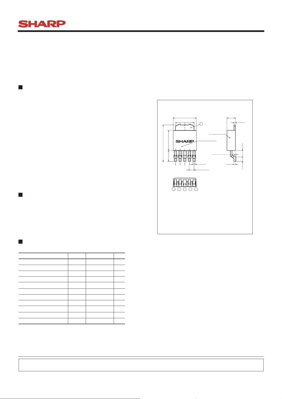
Features Outline Dimensions
■
TO-220 Type Chopper Regulator,
built-in 300kHz oscillation circuit
1.Maximum switching current: 1.5A
2.Built-in ON-OFF control function
3.Built-in soft start function to suppress overshoot of output
5.2
6.6
MAX.
±0.5
voltage in power on sequence or ON/OFF control sequence
4.Built-in oscillation circuit
(Oscillation frequency:TYP.300kHz)
5.Built-in overheat protection function,overcurrent protection
function
6.SC-63 Surface Mount Type package
7.Variable output voltage
(Output variable range: V
ref to 35V/–Vref to –30V)
[Possible to select step-down output/inversing output
MAX.
9.7
±0.5
MIN.
5.5
2.5
1CZ41H
H
according to external connection circuit]
8.P Q1CZ41H2ZZH: Sleeve-packaged product
P Q1CZ41H2ZPH: Tape-packaged product
9.RoHS directive compliant
1 2 3 4 5
Applications
1.Color TV,STB
2.LCD monitors
3.Facsimiles,plinters and other OA equipment
4.CD-ROM drives/DVD-ROM drivers
5.Air conditioners
3
Epoxy resin
Lead finish
identification mark
(0 to 0.25)
+0.2
0.5
-0.1
4-(1.27)
( ) : Typical dimensions
Product mass:(0.3g)
①VIN
②VOUT
③COM(Connected with heat sink)
④O
adj
⑤ON/OFF control
(0.5)
(Unit:mm)
±0.5
2.3
(0.5)
(1.7)(0.9)
Absolute Maximum Ratings
(Composition: Sn2Cu)
(Ta=25℃)
Parameter Symbol Rating Unit
Lead finish:Lead-free solder plating
*1
Input voltage
Error input voltage
Input - output voltage
*2
Output - COM voltage
*3
ON/OFF control voltage
Switching current
*4
Power dissipation P
*5
Junction temperature
Operating temperature
Storage temperature T
Soldering temperature
*1 Voltage between VIN terminal and COM terminal
*2 Voltage between V
*3
Voltage between ON/OFF control and COM terminal
:With infinite heat sink
*4 P
D
*5 There is case that over heat protection function operates at the temperature
j=125
°C
T
Notice The content of data sheet is subject to change without prior notice.
to 150
In the absence of confirmation by device specification sheets, SHARP takes no responsibility for any defects that may occur in equipment using any SHARP
devices shown in catalogs, data books, etc. Contact SHARP in order to obtain the latest device specification sheets before using any SHARP device.
terminal and COM terminal
OUT
°C, so this item cannot be used in this temperature range.
VIN
VADJ
VI-O 41
OUT -1 V
V
VC -0.3 to +40 V
SW 1.5
I
D 8
T
j 150
T
opr
stg
T
sol
40
7
-40 to +85
-40 to +150
260(10s)
W
℃
℃
℃
℃
V
V
V
A
1
Sheet No.: OP06041
Page 2
PQ1CZ41H2ZxH
Electrical Characteristics
Parameter Symbol
Output saturation voltage 0.9 1.5 V
Reference voltage 1.235 1.26 1.285 V
Reference voltage temperature fluctuation
Load regulation |R
Line regulation |RegI| VIN=8 to 35V
Oscillation frequency f
Oscillation frequency temperature fluctuation
Overcurrent detecting level I
Charge current ICHG
Input threshold voltage
Stand-by current
Output OFF-state dissipation current 812
(Unless otherwise specified,condition shall be VIN=12V ,IO=0.2A,VO=5V ,ON-OFF terminals is open,Ta=25℃)
Conditions MIN.
ISW=1AVSAT
Vref
-
Tj=0 to 125℃
egL| IO=0.2 to 1A
-
-
-
-
-
O
L 1.55 2.0 2.6 A
Switching current peak
-
T
j=0 to 125℃
②,④ terminals is open,⑤ terminal
THL
V
VTHH
TH(ON)
Duty ratio=0%,④ terminal=0V,⑤ terminal
Duty ratio=100%,④ terminal =1.1V , ⑤ terminal
④ terminal=0V,⑤ terminal
ISD VIN=40V,⑤ terminal=0V
I
QS VIN=40V,④ terminal=0V ,⑤ terminal =0.9V mA
270 300 330 kHz
-
-
-
-
0.7 0.8 0.9
-
-
TYP.
±0.5
0.2 1.5 %
1.2 2.5 %
84
±3
-10
1.3
2.3
140 400
MAX. Unit
-
-
-
-
-
-
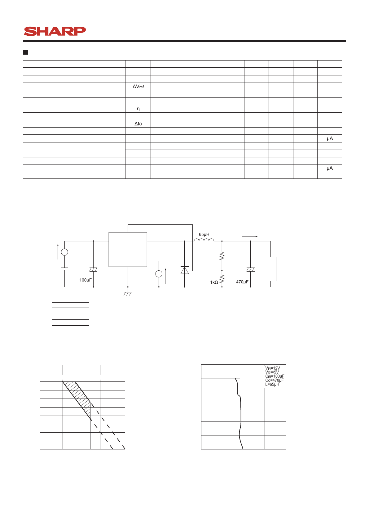
Fig.1 Test Circuit
④
①②
L
I
O
V
O
%
%Efficiency IO=1A
%
V
V
VON threshold voltage V
I
SD
A
A
I
QS
V
IN
ON/OFF control logic
5 pin
LOW
HIGH
OPEN
C
Output
OFF
ON
ON
IN
PQ1CZ41H2ZxH
+
Fig.2 Power Dissipation vs.Ambient
Temperature
10
PD:With infinite heat sink
8
5
Power dissipation PD (W)
R
⑤
③
A
I
CHG
D
L:HK-08S070-6500 (made by Toho Co.)
D:ERC80-004 (made by Fuji electronics Co.)
2
+
C
R
1
O
Load
Fig.3 Overcurrent Protection
Characteristics (Typical Value)
6
5
(V)
O
4
3
2
Output voltage V
1
0
0 25 50 75 100 125
-20
150
Ambient temperature Ta (°C)
Note) Oblique line portion:Overheat protection may operate in this area
0
0123
Output current IO (A)
2
4
Sheet No.: OP06041
Page 3

PQ1CZ41H2ZxH
Fig.4 Efficiency vs. Input Voltage
100
VO=12V,IO=1A
90
VO=12V,IO=0.2A
80
70
VO=5V,IO=0.2A
Efficiency η(%)
60
50
010 203040
VO=5V,IO=1A
Input voltage VIN (V)
Tj=25
°C
Fig.6 Stand-by Current vs. Input Voltage
250
Tj=25
°C
200
(μA)
SD
150
100
Fig.5 Output Saturation Voltage vs.
Switching Current
1.6
1.4
(V)
SAT
1.2
1
0.8
0.6
0.4
0.2
Output saturation voltage V
0
0 0.5 1 1.5
Switching current ISW (A)
Tj=25
°C
Fig.7 Reference Voltage Fluctuation vs.
Junction Temperature
2
1.5
1
0.5
0
-0.5
VIN=12V
O=5V
V
Standby current I
50
0
010 203040
Intput voltage VIN (V)
Fig.8 Load Regulation vs. Output Current
1.5
1
L(%)
eg
0.5
0
Load regulation R
-0.5
0 0.2 0.4 0.6 0.8
Output current IO (A)
Tj=25°C
V
IN=12V
O=5V
V
1 1.2
-1
-1.5
Reference voltage fluctuation (%)
-2
-25 0 25 50 75 100 125-40
Junction temperature Tj (°C)
Fig.9 Line Regulation vs. Input Voltage
1.5
1
0.5
0
Line regulation RegI (%)
-0.5
010203040
Input voltage VIN (V)
Tj=25°C
O=5V
V
O=0.2A
I
Sheet No.: OP06041
3
Page 4

PQ1CZ41H2ZxH
Fig.10 Oscillation Frequency Fluctuation vs.
Junction Temperature
10
5
0
-5
Oscillation frequency fluctuation ΔfO(%)
-10
-25 0 25 50 75 100 125-40
Junction temperature Tj (°C)
VIN=12V
O=5V
V
Fig.12 On Threshold Voltage vs. Junction
Temperature
3
2.5
VTHH
VIN=12V
Fig.11 Overcurrent Detecting Level
Fluctuation vs. Junction Temperature
10
5
0
-5
Overcurrent detecting level fluctuation (%)
-10
-25 0 25 50 75 100 125-40
Junction temperature Tj (°C)
Tj=25°C
Fig.13 Operating Dissipation Current vs.
Input Voltage
10
Tj=25°C
O=5V
' (mA)
Q
9
V
2
VTHL
1.5
1
0.5
VTHON
ON threshold voltage VTHON,VTHL,VTHH (V)
0
-25 0 25 50 75 100 125-40
Junction temperature Tj (°C)
Fig.14 Power Dissipation vs. Ambient
Temperature (Typical Value)
Cu area 740mm
2
(W)
D
Cu area 180mm
1.5
Cu area 100mm
Cu area 70mm
1
Cu area 36mm
0.5
Power dissipation P
2
2
2
2
2
8
IO=0.2A
7
6
Operating dissipation current I
5
010 203040
IO=1A
No Load
Input voltage VIN (V)
Mounting PCB
PCB
Cu
Material : Glass-cloth epoxy resin
Size
Cu thickness
: 50×50×1.6mm
: 35μm
0
-20 0 20 40 60 80 100-40 120
Ambient temperature Ta (°C)
12585
Sheet No.: OP06041
4
Page 5

Fig.15 Block Diagram
1
V
IN
PQ1CZ41H2ZxH
2
V
OUT
Voltage
regulator
PWM COMP.
Overcurrent
detection
circuit
Overheat
detection
circuit
F/F
3
Q
R
S
COM
Fig.16 Step Down Type Circuit Diagram
④
①②
PQ1CZ41H2ZxH
+ +
V
IN
8 to 35V
C
IN
③
ON/OFF
_
+
circuit
Oscillator
Soft start
ERROR AMP.
_
+
V
ref
5
ON/OFF control
4
O
adj
L
V
O
5V
R
⑤
R
C
S
S
D
2
3k
Load
C
O
R
1
1k
ON/OFF control signal
Fig.17 Polarity Inversion Type Circuit Diagram
0.47~1μF
100k~
680kΩ
1
V
IN
5~30V
+
C
IN
100μF
In case that polarity is reverse, depending on the conditions,there is cases that output voltage can not gain,
please use this device after confirming the output voltage at the actual conditions.
4
PQ1CZ41H2ZxH
3
2
5
C
S
R
S
D
ON/OFF control signal
L
65μH
R
3kΩ
R
1kΩ
2
1
R
S
≦50kΩ
O
C
2200μF
+
Load
V
O
-5V
Sheet No.: OP06041
5
 Loading...