

Page 1
Chopper Regulators PQ1CG21H2FZ/PQ1CG21H2RZ
PQ1CG21H2FZ/PQ1CG21H2RZ
TO-220 Type Chopper Regulators
Features
■
●
Maximum switching current: 1.5A
●
Built-in ON/OFF control function
●
Built-in soft start function to suppress overshoot of output
voltage in power on sequence or ON/OFF control sequence
●
Built-in oscillation circuit
(Oscillation frequency: TYP. 100kHz)
●
Built-in overheat, overcurrent protection functions
●
TO-220 package
●
Variable output voltage
(Output variable range: Vref to 35V/-Vref to -30V)
[Possible to select step-down output/inversing output
according to external connection circuit]
●
PQ1CG21H2FZ: Zigzag forming
PQ1CG21H2RZ: Self-stand forming
Applications
■
●
Switching power supplies
●
Facsimiles, printers and other OA equipment
●
Color TVs and video CDs
●
Personal computers and amusement equipment
Absolute Maximum Ratings
■
(Ta=25°C)
Parameter Symbol Rating Unit
❇1
Input voltage
Error input voltage
Input-output voltage
❇2
Output − COM voltage
❇3
ON/OFF control voltage
Switching current
❇4
Power dissipation
❇5
Junction temperature
Operating temperature
Storage temperature
Soldering temperature
❇1 Voltage between VIN terminal and COM terminal
❇2 Voltage between V
❇3 Voltage between ON/OFF control and COM terminal
:With infinite heat sink
❇4 P
D
❇5 Overheat protection may operate at the condition T
terminal and COM terminal
OUT
V
IN
V
ADJ
V
I-O
V
OUT
V
C
I
SW
P
D1
D2
T
j
T
opr
T
stg
T
sol
40
7
41
−1
−0.3 to +40
1.5
1.4
14 WP
150
−20 to +80
−40 to +150 ˚C
260 (10s) ˚C
:125˚C to 150˚C.
j
W
˚C
˚C
8.2
(0.5)
4.7
4.5
±0.6
±0.7
4.5
±0.2
1
2
3
4
5
1
2
3
4
5
(Unit : mm)
±0.2
2.8
±0.5
5.0
(2.0)
(1.5)
MIN.
4.4
±0.5
3.2
V
IN
V
OUT
COM
O
ADJ
ON/OFF
±0.2
±0.2
2.8
(2.2)
(1.7)
±0.6
4.7
±0.5
2.6
V
IN
V
OUT
COM
O
ADJ
ON/OFF
±0.7
16.4
(11.4)(3.6)
±0.5
6.0
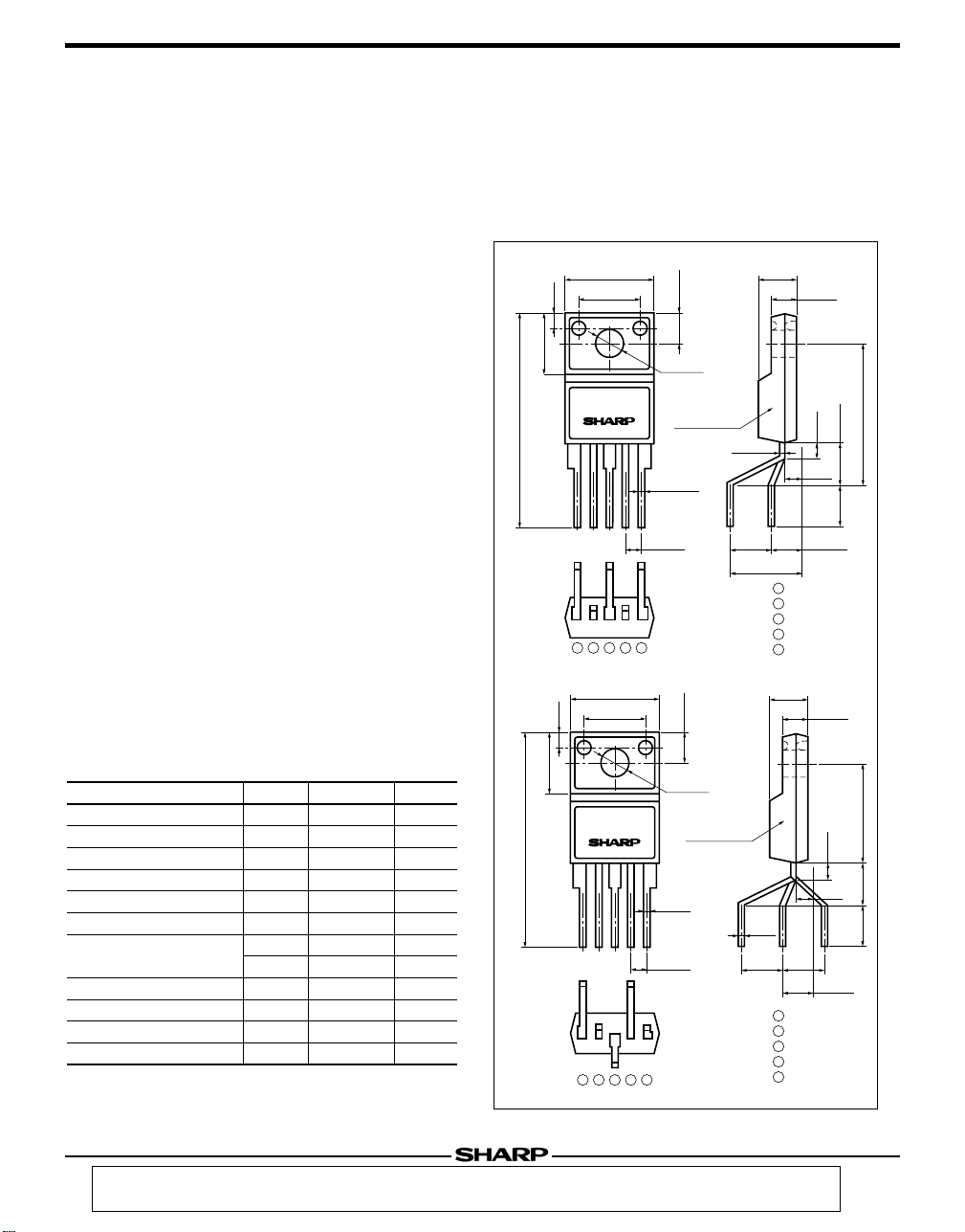
Outline Dimensions
■
PQ1CG21H2FZ
(1.5)
±0.2
7.4
(24.6)
PQ1CG21H2RZ
±0.2
7.4
V
V
V
(24.6)
10.2
PQ1CG21H
1 2 3 4 5
(1.5)
PQ1CG21H
(6.8)
10.2
MAX.
(6.8)
MAX.
ø3.2
5–0.8
4–(1.7)
ø3.2
±0.2
3.6
±0.1
Epoxy resin
(0.5)
±0.1
(5.0)
( ) : Typical dimensions
±0.2
3.6
±0.1
Epoxy resin
V
V
0.8
±0.1
A
4–(1.7)
1 2 3 4 5
•Please refer to the chapter " Handling Precautions ".
( ) : Typical dimensions
Notice In the absence of confirmation by device specification sheets,SHARP takes no responsibility for any defects that may occur in equipment using any SHARP
devices shown in catalogs,data books,etc.Contact SHARP in order to obtain the latest device specification sheets before using any SHARP device.
Internet Internet address for Electronic Components Group http://sharp-world.com/ecg/
Page 2
Chopper Regulators PQ1CG21H2FZ/PQ1CG21H2RZ
Electrical Characteristics
■
Parameter Symbol Conditions
Output saturation voltage
Reference voltage
Reference voltage temperature fluctuation
Load regulation
Line regulation
Efficiency
Oscillation frequency
Oscillation frequency temperature fluctuation
Overcurrent detecting level
Charge current
Input threshold voltage
ON threshold voltage
Stand-by current
Output OFF-state dissipation current
Fig.1 Test Circuit
(Unless otherwise specified, condition shall be V
V
SAT
V
ref
∆V
|RegL|
|R
eg
ref
I|
j
=0 to 125˚C
T
O
I
IN
V
η
f
O
∆f
O
I
L
, terminals is open, terminal
CHG
I
Duty ratio=0%, terminal=0V, terminal
V
THL
Duty ratio=100%, terminals is open, terminal
V
THH
TH(ON)
V
I
SD
I
QS
Tj=0 to 125˚C
42 5
4 5
terminal=0V, terminal
IN
=40V, terminal=0V
V
VIN=40V, terminal=0.9V
I
SW
=1A
−
=0.2 to 1A
=8 to 35V
O
=1A
I
−
−
5
5
IN
=12V, IO=0.2A, VO=5V, ON-OFF terminals is open,
54
54
Ta=25˚C)
1.5
1.285
−
1.5
2.5
−
120
2.6
Unit
V
V
%
%
%
%
kHz
%
A
µA
V
V
V
MIN.
−
1.235
−
−
−
−
80
−−
1.55
−
−
−
MAX.TYP.
1.0
1.26
±0.5
0.2
0.5
84
100
±2
2.0
−10 −
1.3 −
2.3 −
0.7 0.8 0.9
− 140 400 µA
− 812mA
4
12
I
SD
A
A
I
QS
+
V
V
IN
IN
C
IN
100µF
PQ1CG21H2
3
Fig.2 Power Dissipation vs. Ambient
Temperature
20
15
P
: With infinite heat sink
(W)
D
Power dissipation P
Note) Oblique line portion:Overheat protection may operate in this area
D2
10
5
P
: No heat sink
D1
0
−200 20406080100
Ambient temperature T
(°C)
a
L
210µH
R
5
A
I
CHG
D
2
R
1
1kΩ
L : HK-14S100-2110 (made by Toho Co.)
D :ERC80-004 (made by Fuji electronics Co.)
C
470µF
I
O
O
V
O
+
Load
Fig.3 Overcurrent Protection
Characteristics (Typical Value)
6
Ta=25°C
=12V
5
(V)
4
O
3
2
Output voltage V
1
0
01234
Output current IO (A)
V
IN
=5V
V
O
Page 3

Chopper Regulators PQ1CG21H2FZ/PQ1CG21H2RZ
Line regulation R
eg
I
(%)
Input voltage V
IN
(V)
−0.5
0
0.5
1
1.5
5 10152025303540
Tj=25°C
V
O
=5V
I
O
=0.2A
Fig.4 Efficiency vs. Input Voltage Fig.5 Output Saturation Voltage vs.
Switching Current
100
VO=12V, IO=1A
VO=12V, IO=0.2A
Tj=25°C
90
(%)
80
VO=5V, IO=1A
70
Efficiency η
VO=5V, IO=0.2A
60
50
5 15253545
Input voltage V
(V)
IN
1.4
1.2
(V)
SAT
1
0.8
0.6
0.4
Output saturation voltage V
0.2
0
0 0.5 1 1.5 2
Switching current I
SW
Tj=25°C
(A)
Fig.6 Stand-by Current vs. Intput Voltage Fig.7 Reference Voltage Fluctuation vs.
Junction Temperature
250
200
(µA)
SD
150
100
2
VIN=12V
=5V
V
O
1
0
Stand−by current I
50
0
0 5 10 15 20 25 30 4035
Intput voltage V
Fig.8 Load Regulation vs. Output Current Fig.9 Line Regulation vs. Input Voltage
1
0.5
L(%)
eg
0
Load regulation R
−0.5
0 0.2 0.4 0.6 0.8 1 1.2
Output current IO (A)
−1
Reference voltage fluctuation (%)
−2
−20 0 20 40 60 80 100 120
(V)
IN
Junction temperature T
(°C)
j
Tj=25°C
=12V
V
IN
=5V
V
O
Page 4

Chopper Regulators PQ1CG21H2FZ/PQ1CG21H2RZ
j
Fig.10 Oscillation Frequency Fluctuation vs.
Junction Temperature
2
VIN=12V
=5V
V
O
0
−2
−4
−6
−8
Oscillation frequency fluctuation (%)
−10
−20 0 20 40 60 80 100 120
Junction temperature T
(°C)
j
Fig.12 Threshold Voltage vs. Junction
Temperature
3
(V)
TH (H)
V
TH (L) ,
V
TH (ON) ,
2.5
1.5
V
TH(H)
2
V
TH(L)
1
VIN=12V
Fig.11 Overcurrent Detecting Level
Fluctuation vs. Junction Temperature
6
4
2
0
−2
−4
−6
Overcurrent detecting level fluctuation (%)
−8
−20
0 20406080100120
Junction temperature T
(°C)
j
Fig.13 Operating Dissipation Current vs.
Input Voltage
' (mA)
Q
10
9
=1A
I
8
7
=0.2A
I
O
O
Tj=25°C
=5V
V
O
0.5
Threshold voltage V
0
−50 0 50 100 150−25 25 75 125
V
TH(ON)
Junction temperature T
Fig.14 Block Diagram
1
V
IN
Overcurrent
detection
circuit
Overheat
detection
circuit
(°C)
Voltage
regulator
PWM COMP.
F/F
3
Q
S
R
COM
ON/OFF
circuit
_
+
Oscillator
6
Operating dissipation current I
5
Soft start
ERROR AMP.
_
+
V
ref
No load
0 10203040
Input voltage V
2
V
OUT
5
ON/OFF
4
V
ADJ
(V)
IN
Page 5

Chopper Regulators PQ1CG21H2FZ/PQ1CG21H2RZ
Fig.15 Step Down Type Circuit Diagram
4
12
PQ1CG21H2
5
+ +
V
IN
8 to 35V
C
IN
100µF
3
C
S
ON/OFF control signal RS≤50kΩ
Fig.16 Polarity Inversion Type Circuit Diagram
4
V
5 to 30V
1
PQ1CG21H2
+
IN
C
IN
100µF
3
2
5
C
S
L
210µH
R
2
3kΩ
R
S
D
R
1
1kΩ
L
130µH
R
2
3kΩ
R
S
D
R
1
1kΩ
C
470µF
C
2 200µF
VO5V
Load
O
+
Load
O
ON/OFF control signal RS≤50kΩ
V
O
−5V
Page 6

NOTICE
●
The circuit application examples in this publication are provided to explain representative applications of SHARP
devices and are not intended to guarantee any circuit design or license any intellectual property rights. SHARP takes
no responsibility for any problems related to any intellectual property right of a third party resulting from the use of
SHARP's devices.
●
Contact SHARP in order to obtain the latest device specification sheets before using any SHARP device. SHARP
reserves the right to make changes in the specifications, characteristics, data, materials, structure, and other contents
described herein at any time without notice in order to improve design or reliability. Manufacturing locations are
also subject to change without notice.
●
Observe the following points when using any devices in this publication. SHARP takes no responsibility for damage
caused by improper use of the devices which does not meet the conditions and absolute maximum ratings to be used
specified in the relevant specification sheet nor meet the following conditions:
(i) The devices in this publication are designed for use in general electronic equipment designs such as:
--- Personal computers
--- Office automation equipment
--- Telecommunication equipment [terminal]
--- Test and measurement equipment
--- Industrial control
--- Audio visual equipment
--- Consumer electronics
(ii) Measures such as fail-safe function and redundant design should be taken to ensure reliability and safety when
SHARP devices are used for or in connection with equipment that requires higher reliability such as:
--- Transportation control and safety equipment (i.e., aircraft, trains, automobiles, etc.)
--- Traffic signals
--- Gas leakage sensor breakers
--- Alarm equipment
--- Various safety devices, etc.
(iii)SHARP devices shall not be used for or in connection with equipment that requires an extremely high level of
reliability and safety such as:
--- Space applications
--- Telecommunication equipment [trunk lines]
--- Nuclear power control equipment
--- Medical and other life support equipment (e.g., scuba).
●
Contact a SHARP representative in advance when intending to use SHARP devices for any "specific" applications
other than those recommended by SHARP or when it is unclear which category mentioned above controls the
intended use.
●
If the SHARP devices listed in this publication fall within the scope of strategic products described in the Foreign
Exchange and Foreign Trade Control Law of Japan, it is necessary to obtain approval to export such SHARP devices.
●
This publication is the proprietary product of SHARP and is copyrighted, with all rights reserved. Under the copyright
laws, no part of this publication may be reproduced or transmitted in any form or by any means, electronic or
mechanical, for any purpose, in whole or in part, without the express written permission of SHARP. Express written
permission is also required before any use of this publication may be made by a third party.
●
Contact and consult with a SHARP representative if there are any questions about the contents of this publication.
 Loading...