

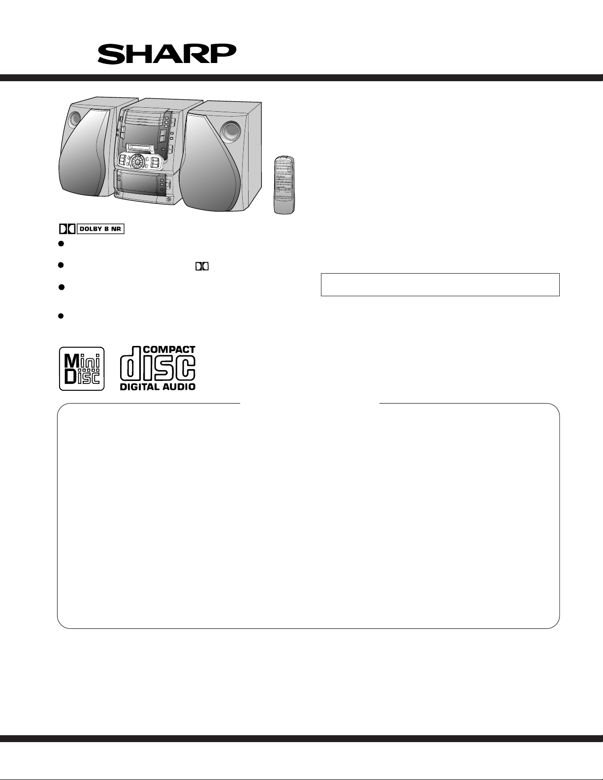
Page 1
SERVICE MANUAL
Dolby noise reduction manufactured under license from Dolby
Laboratories Licensing Corporation.
"DOLBY" and the double-D symbol are trademarks of Dolby
Laboratories Licensing Corporation.
It is the intent of Sharp that this product be used in full compliance
with the copyright laws of the United States and that prior permission
be obtined from copyright owners whenever necessary.
US and foreign patents licensed from Dolby Laboratories Licensing
Corporation.
MD-X60
No.S6839MDX60///
MD-X60
• In the interests of user-safety the set should be restored to its original
condition and only parts identical to those specified should be used.
CONTENTS
Page
IMPOTANT SERVICE NOTES .......................................................................................................................................... 2
SPECIFICATIONS ............................................................................................................................................................. 2
NAMES OF PARTS ........................................................................................................................................................... 3
OPERATION MANUAL ...................................................................................................................................................... 6
QUICK GUIDE ................................................................................................................................................................... 8
DISASSEMBLY.................................................................................................................................................................. 9
REMOVING AND REINSTALLING THE MAIN PARTS................................................................................................... 13
ADJUSTMENT ................................................................................................................................................................. 16
WIRING DIAGRAM .......................................................................................................................................................... 30
BLOCK DIAGRAM ........................................................................................................................................................... 32
SCHEMATIC DIAGRAM / WIRING SIDE OF P.W.BOARD............................................................................................. 36
NOTES ON SCHEMATIC DIAGRAM .............................................................................................................................. 62
TYPE OF TRANSISTOR AND LED ................................................................................................................................. 62
WAVEFORMS OF CD CIRCUIT...................................................................................................................................... 63
WAVEFORMS OF MD CIRCUIT ..................................................................................................................................... 64
TROUBLESHOOTING (CD SECTION) ........................................................................................................................... 66
TROUBLESHOOTING (MD SECTION) ........................................................................................................................... 70
FUNCTION TABLE OF IC................................................................................................................................................ 75
REPLACEMENT PARTS LIST/EXPLODED VIEW/PACKING OF THE SET
SHARP CORPORATION
– 1 –
This document has been published to be used
for after sales service only.
The contents are subject to change without notice.
Page 2
MD-X60
FOR A COMPLETE DESCRIPTION OF THE OPERATION OF THIS UNIT, PLEASE REFER
TO THE OPERATION MANUAL.
IMPORTANT SERVICE NOTES
BEFORE RETURNING THE AUDIO PRODUCT
(Fire & Shock Hazard)
Before returning the audio product to the user, perform the following
safety checks.
1. Inspect all lead dress to make certain that leads are not pinched
or that hardware is not lodged between the chassis and other
metal parts in the audio product.
2. Inspect all protective devices such as insulating materials, cabinet,
terminal board, adjustment and compartment covers or shields,
mechanical insulators etc.
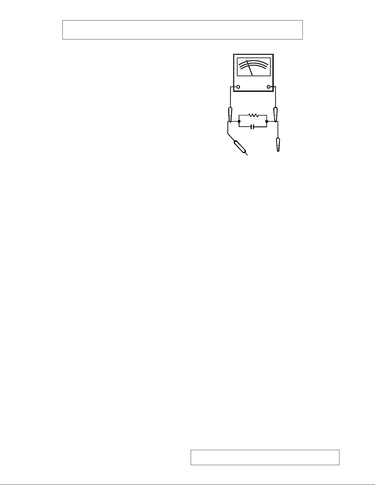
3. To be sure that no shock hazard exists, check for leakage current
in the following manner.
* Plug the AC line cord directly into a 120 volt AC outlet.
* Using two clip leads, connect a 1.5k ohm, 10 watt resistor paralleled
by a 0.15µF capacitor in series with all exposed metal cabinet
parts and a known earth ground, such as conduit or electrical
ground connected to earth ground.
* Use a VTVM or VOM with 1000 ohm per volt, or higher, sensitivity
to measure the AC voltage drop across the resistor (See diagram).
* Connect the resistor connection to all exposed metal parts having
a return path to the chassis (antenna, metal cabinet, screw heads,
knobs and control shafts, escutcheon, etc.) and measure the AC
voltage drop across the resistor.
VTVM
AC SCALE
1.5k ohms
10W
0.15 µ F
TO EXPOSED
METAL PARTS
TEST PROBE
CONNECT TO
KNOWN EARTH
GROUND
All check must be repeated with the AC line cord plug connection
reversed.
Any reading of 0.3 volt RMS (this corresponds to 0.2 milliamp. AC.)
or more is excessive and indicates a potential shock hazard which
must be corrected before returning the audio product to the owner.
SPECIFICATIONS
● MiniDisc recorder section
Type: MiniDisc recorder
Signal readout: Non-contact, 3-beam semi-conductor laser
Audio channel: Stereo; 2 channels
Frequency response: 20 - 20,000 Hz
Rotation speed: 400 - 900 rpm CLV, Approx
Quantization: 16-bit linear
Filter: 8-times oversampling digital filter
Error correction: ACIRC (Advanced Cross Interleave Reed-
Coding: ATRAC (Adaptive TRansform Acoustic
Recording method: Magnetic modulation overwrite method
D/A converter: 1-bit D/A converter
Sampling frequency: 44.1 kHz
Wow and flutter: Unmeasurable
Signal/noise ratio: 95 dB (1 kHz)
Dynamic range: 90 dB (1 kHz)
● Compact disc player section
Type: 3-disc multi-play compact disc player
Signal readout: Non-contact, 3-beam semi-conductor laser
Rotation speed: 200 - 500 rpm CLV, Approx.
Error correction: CIRC (Cross Interleave Reed-Solomon
Quantization: 16-bit linear
D/A converter: 1-bit D/A converter
Filter: 8-times oversampling digital filter
Frequency response: 20 - 20,000 Hz
Signal/noise ratio: 95 dB (1 kHz)
Dynamic range: 90 dB (1 kHz)
Wow and flutter: Unmeasurable
● Tuner section
Frequency range: FM; 87.5 - 108 MHz
Sensitivity: FM; 2.5 µV (75 ohms unbalanced)
pickup
Monaural; 1 channel (long-time recording
mode)
Solomon Code)
Coding)
(less than 0.001% W. peak)
pickup
Code)
(less than 0.001% W. peak)
AM; 530 - 1,720 kHz
AM; 650 µV/m
● Cassette deck section
Type: Compact cassette tape
Frequency response: 50 - 14,000 Hz (Normal tape)
Motor: DC motor with electronic governor × 1
Signal/noise ratio: 50 dB (Recording/Playback, Dolby NR off)
Bias and erasure
system: AC
Tape speed: 1-7/8 ips. (4.76 cm/sec.)
Wow and flutter: 0.15 % (WRMS)
Heads: Record/playback × 1
50 - 15,000 Hz (CrO
Dolby NR effect; 10 dB
(at over 5 kHz)
Erase × 1
2
tape)
● General
Power source: AC 120 V, 60 Hz
Power consumption: 101 W
Output power: 40 watts per channel minimum RMS into 6
Input terminals: MD IN/AUX (Analog-1); 500 mV/47 kohms
Output terminals: Auxiliary; 2.0 V/1 kohm
Dimensions: Width; 9-1/2" (240 mm)
Weight: 19.0 lbs. (8.6 kg)
ohms from 60 Hz to 20 kHz with no more
than 10 % total harmonic distortion
Auxiliary (Analog-2); 500 mV/47 kohms
Auxiliary (Digital); optical
Headphones; 16 - 50 ohms
(recommended; 32 ohms)
Speakers; 6 ohms
Height; 13-1/8" (332 mm)
Depth; 12-13/16" (325 mm)
● Speaker section
Type: 3-way type [6" (150 mm) woofer, 2-1/2" (65
Maximum input power: 100 W
Rated input power: 50 W
Impedance: 6 ohms
Dimensions: Width; 8-1/8" (205 mm)
Weight: 9.3 lbs. (4.2 kg)/each
mm) tweeter and super tweeter]
Height; 13-1/8" (332 mm)
Depth; 12-3/4" (323 mm)
Specifications for this model are subject to change without
prior notice.
– 2 –
Page 3
NAMES OF PARTS
Front panel
11. Power Button: POWER
12. Tuner Call (Band Select) Button: TUNER (BAND)
13. Preset Equalizer Button: PRE-EQ
14. Extra Bass Button: X-BASS
15. Auxiliary Input (Digital/Analog) Select Button: AUX
16. MD Compartment
17. Sampling Frequency Indicators
18. (CD) Open/Close Buttons:
19. (CD) Play Buttons: 1 , 2 , 3
10. (CD) Play/Pause Button and Indicator:
11. (CD) Stop Button:
12. Volume Up/Down Buttons: VOLUME /
13. (MD) Record Button: REC
14. Sound Synchro Record Button
15. (MD) Play/Pause Button:
16. (MD) Stop Button:
17. (MD) Eject Button:
18. CD MD Edit Button: CD MD
19. MD MD Edit Button: MD MD
20. TAPE MD Edit Button: TAPE MD
21. (CD/MD) Track Edit Button: TRACK EDIT
22. Timer/Delete Button: TIMER/DELETE
23. Display Button: DISPLAY
24. (MD) Record Mode Button: REC MODE
25. (MD) Pole Position Button: POLE POSITION
26. CD TAPE Edit Button: CD TAPE
27. MD TAPE Edit Button: MD TAPE
28. (MD) Name/TOC-Edit Button: NAME/TOC EDIT
29. (TUNER) Tuning Down Button:
3 (CD) Track Down/Review Button:
3 (MD) Track Down/Review/Cursor Button:
30. Jog Dial
31. (TUNER) Tuning Up Button:
3 (CD) Track Up/Cue Button:
3 (MD) Track Up/Cue/Cursor Button:
1
2
3
4
5
6
7
33
34
35
18
19
20
21 22
28 29
41
30
42
23
31
8
MD-X60
9
10
11
12
13
14
15
16
17
24
25
26
27
32
36
37
38
39
40
43
32. Enter Button: ENTER
33. (TAPE) Dolby NR Button: DOLBY NR
34. (TAPE) Reverse Mode Button: REVERSE MODE
35. MD Edit/Auxiliary 1 (Analog) Input Jack: MD IN/AUX 1
36. (TAPE) Fast Wind Buttons: /
37. (TAPE) Forward Play Button:
38. (TAPE) Stop Button:
39. (TAPE) Reverse Play Button:
40. (TAPE) Record Pause Button:
41. Auxiliary Input Level (Analog) Control: INPUT LEVEL
42. Cassette Compartment
43. Headphone Jack: PHONES
Rear panel
11. Auxiliary Digital Input Jack (Optical)
12. 75 Ohm FM Antenna Terminal
13. FM Antenna Ground Terminal
14. AM Antenna Ground Terminal
15. AM Antenna Terminal
16. Reset Button
17. Speaker Terminals
18. AUX 2 (Analog) Input Jacks
19. Analog Output Jacks
10. Beat Cancel Switch
11. AC Power Cord
1
2
3
4
5
6
7
8
9
11
10
– 3 –
Page 4
MD-X60
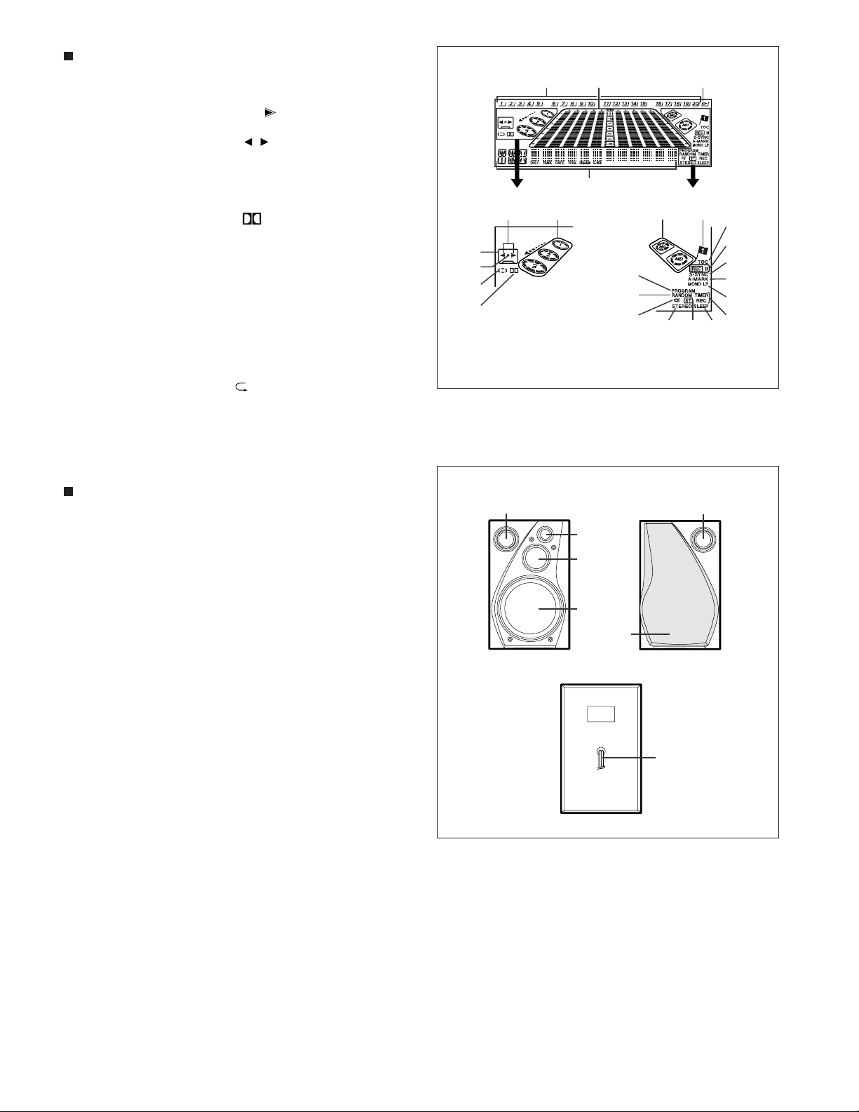
Display window
11. (CD/MD) Music Schedule Indicators
12. Level Meters
13. (CD/MD) More Tracks Indicator:
14. Character Information Display
15. (TAPE) Direction Indicators: /
16. CD Indicator
17. (TAPE) Loading Indicator
18. (TAPE) Recording Indicator
19. (TAPE) Reverse Mode Indicator
10. (TAPE) Dolby NR Indicator:
11. MD Indicator
12. Pole Position Record Indicator
13. (MD) TOC Indicator: TOC
14. (MD) Record Indicator: REC
15. (MD) Sound Synchro Indicator: S.SYNC
16. (MD) Auto Mark Indicator: AUTO MARK
17. (MD) Recording Mode Indicator: MONO LP
18. Timer Play/Timer Record Indicator
19. (CD/MD) Program Indicator: PROGRAM
20. (CD/MD) Random Play Indicator: RANDOM
21. (CD/MD) Repeat Indicator:
22. FM Stereo Mode Indicator: STEREO
23. FM Stereo Indicator: ST
24. Sleep Indicator: SLEEP
7
8
9
10
1
2
3
4
12
19
20
21
11
13
14
15
16
17
18
242322
5
6
Speaker section
11. Bass Reflex Duct
12. Super Tweeter
13. Tweeter
14. Woofer
15. Speaker Grille
16. Speaker Wire
1
1
2
3
4
5
6
– 4 –
Page 5
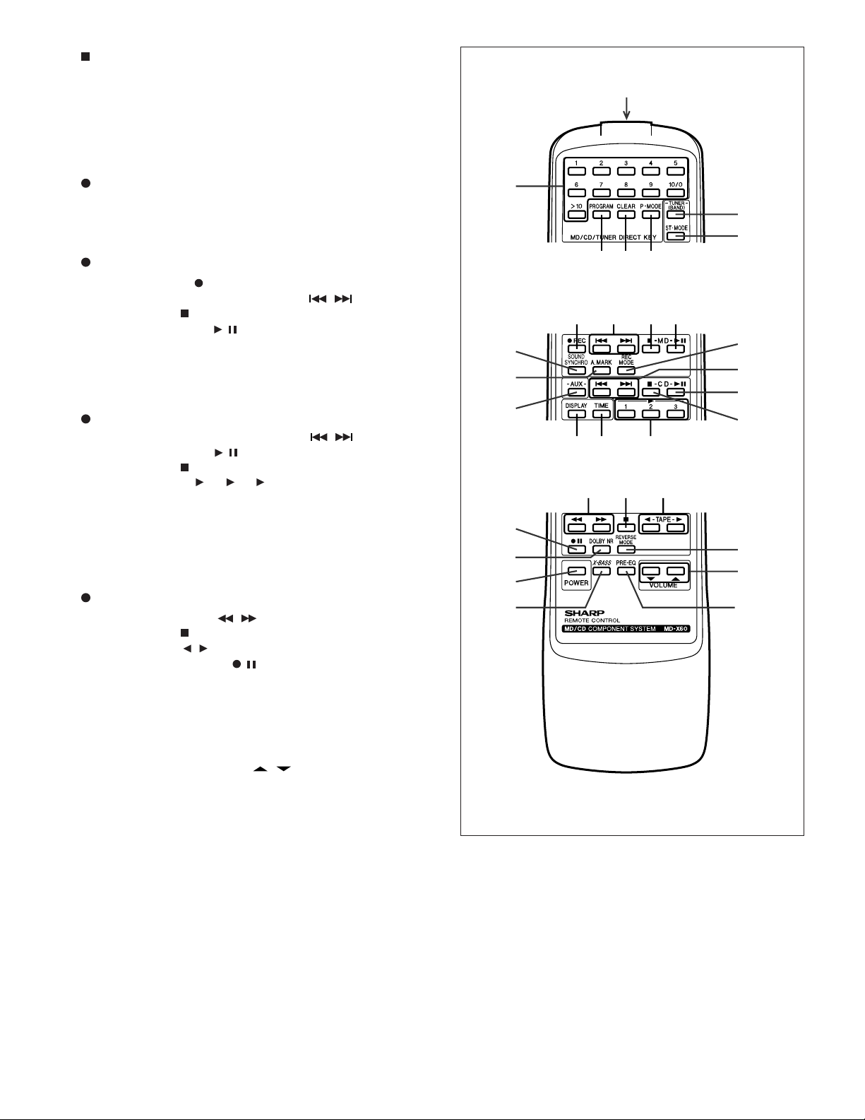
Remote control
11. Remote Control Transmitter LED
12. (MD/CD/TUNER) Direct Key
13. (CD/MD) Program Button: PROGRAM
14. (CD/MD) Program Clear Button: CLEAR
15. (CD/MD) Play Mode Button: P-MODE
MD-X60
1
Tuner control section
16. Tuner Call (Band Select) Button: TUNER/BAND
17. FM Stereo Mode Button: ST MODE
MD control section
18. Record Button: REC
19. Track Up,Cue/Down,Review Buttons: /
10. Stop Button:
11. Play/Pause Button:
12. Sound Synchro Record Button: S.SYNC
13. Auto Mark Button: A.MARK
14. Record Mode Button: REC MODE
CD control section
15. Track Up,Cue/Down,Review Buttons: /
16. Play/Pause Button:
17. Stop Button:
18. Play Buttons: 1 , 2 , 3
19. Auxiliary Input (Digital/Analog) Select Button: AUX
20. Display Button: DISPLAY
21. Time Display Select Button: TIME
Tape control section
22. Fast Wind Buttons: /
23. Stop Button:
24. Play Buttons: /
25. Record Pause Button:
26. Dolby NR Button: DOLBY NR
27. Reverse Mode Button: REVERSE MODE
2
12
13
19
25
26
28
29
3
8
21
20
22 23
6
7
4
5
9
10
11
14
15
16
17
18
24
27
30
31
28. Power Button: POWER
29. Extra Bass Button: X-BASS
30. Volume Up/Down Buttons: /
31. Pre-programed Equalizer Button: PRE-EQ
– 5 –
Page 6
MD-X60
SETTING THE CLOCK
(Main unit operation)
1
Press the POWER button to turn the power on.
2
Press the TIMER/DELETE button.
3
Within 10 seconds, turn the jog dial until "TIME ADJUST" appears.
4
Within 10 seconds, press the ENTER button.
The unit will enter the date setting mode.
5
Adjust the "month" using the jog dial.
When you turn the jog dial and let go, the month will change up or down by
one. When you turn and hold it, the month will change continuously.
6
Press the ENTER button to set the "month".
7
Adjust the "day" using the jog dial.
8
Press the ENTER button to set the "day".
9
Adjust the "year" using the jog dial.
The year 2000 or later is set as follows:
[00] indicates the year 2000.
[01] indicates the year 2001.
The range of dates that can be entered is from January 1, 1997 to December
31, 2099.
10
Press the ENTER button to set the "year".
The unit will enter the time setting mode.
11
Adjust the "hour" using the jog dial.
When you turn the jog dial and let go, the hour will change up or down by one.
When you turn and hold it, the hour will change continuously.
On the display, midnight is "AM 12:00" and noon is "PM 12:00". When setting
the time, be careful not to confuse AM and PM.
12
Press the ENTER button to set the "hour".
13
Adjust the "minute" using the jog dial.
14
Press the ENTER button to set the "minute".
The clock starts operating from "0" seconds. (Seconds are not displayed.)
POWER
TIMER /
DELETE
ENTER
2
14
12
13
3
4
5
6
7
8
9
10
11
Notes:
In the event of a power failure or when the AC power cord is disconnected, the
clock setting will be lost. Reset the time.
While recording an MD, you cannot set the date and clock. Be sure to set the
date and clock before recording.
Resetting the date and time:
Once you have set the date and time, "TIME ADJUST" will not be displayed in
step 2. Turn the jog dial to make the date and time appear.
If you don't need to change the settings, just press the ENTER button without
turning the jog dial again.
Checking the date and time:
Press the TIMER/DELETE button. Then turn the jog dial until the date and time
are displayed.
Press the DISPLAY button to switch between the date and the time.
After about 10 seconds, the original display will appear.
Once the date and the time have been set, this unit will normally display the
time when the unit is in the stand-by mode.
To check the date, press the DISPLAY button.
The display will switch between the date and the time each time you press the
button.
Jog dial
Date setting mode
Time setting mode
MINIDISC SYSTEM LIMITATIONS
Even if the maximum recording time of a MiniDisc has not
been reached, "TOC FULL" may be displayed.
Even if the maximum recording time of a MiniDisc has not
been reached, "DISC FULL" may be displayed.
Even if several short tracks are erased, the remaining
recording time may not show an increase.
Two tracks may not be combined in editing.
The total of the recorded time and time remaining on a
disc may not add up to the maximum possible recording
time.
If recorded tracks are fast reversed or fast forwarded, the
sound may skip.
In the MD system, the delimiter of the recording area on an MD is programmed
in a TOC. If partial erasing, recording and editing are repeated several times,
TOC information will fill up, even though the number of tracks has not reached
the limit (255 tracks), and further recording will be impossible. (If you use the all
erase function, this MD can be used from the beginning.)
If there is any flaw on the MiniDisc, that part is automatically excluded from the
space available for recording. Therefore, the recording time becomes shorter.
When the remaining recording time of a disc is displayed, short tracks less than
12 seconds long may not be included in the total.
For MiniDiscs on which repeated recording and editing operations were per-
formed, the COMBINE function may not work.
A track recorded from a CD (digital recording) and a track recorded from a radio
or other equipment (analog recording) cannot be combined.
A cluster (about 2 seconds) is normally the minimum unit of recording. So, even
if a track is less than 2 seconds long, it will use about 2 seconds of space on
the disc. Therefore, the time actually available for recording may be less than
the remaining time displayed.
If there are scratches on discs, those sections will be automatically avoided (no
recording will be placed in those sections). Therefore, the recording time will be
reduced.
An MD which has been recorded or edited repeatedly may skip during fast reverse
or fast forward.
TROUBLESHOOTING
If a problem occurs
If this unit functions abnormally during operation, first check the following items. If the unit continues to function abnormally, or if an abnormality
appears other than listed below, turn off the player's power and disconnect the AC power plug, then consult your SHARP dealer or service
personnel.
General
SYMPTOM
POSSIBLE CAUSE REMEDY
The clock is wrong.
Did a power failure occur?
Try setting it again.
When a button is pressed, the unit does
not respond.
Set this unit to the stand-by mode and then
turn it back on. Then, retry the operation.
No sound is heard.
Is the volume level is set to "0"?
Are the headphones connected?
Are the speaker wires disconnected?
Increase the volume level.
Disconnect the headphones.
Connect the wires securely.
Radios make unusual noise or the picture
on the TV screen is distorted.
When a radio or TV which uses an indoor
antenna is placed near the unit, the picture
on the TV screen may be distorted or the
radio may not function properly.
It is recommended that you use an external
antenna.
CD playback
SYMPTOM
POSSIBLE CAUSE REMEDY
Even though a disc has been loaded, "NO
DISC" or "ERR" is displayed.
Playback stops in the middle of a track, or
playback is not performed properly.
Playback sounds are skipped.
The disc is loaded up-side down.
The disc is very dirty.
The disc which does not satisfy the stand-
ards.
Is the unit located near excessive vibra-
tions?
Has condensation formed inside the unit?
Load the disc with the correct side up.
Clean the disc.
Load the correct disc.
Place the unit on a firm, level surface free
from vibration.
Remove the disc and leave the power
turned on. The unit should function properly
in about 1 hour.
OPERATION MANUALNAMES OF PARTS
– 6 –
Page 7
MD-X60
(Continued)
MD recording and playback
SYMPTOM
POSSIBLE CAUSE
REMEDY
A recording cannot be made.
Is the MiniDisc protected against accidental
erasure?
Did you tr y to make recordin g on a
playback-only MiniDisc?
Can you see the "TOC FULL" message in
the display?
Slide the accidental erase prevention tab
back to its original position.
Replace it with a recordable disc.
Put in another recordable disc with record-
ing space on it.
Even though a disc has been loaded, "NO
DISC" or "ERR" is displayed.
Playback sounds are skipped.
The disc is very dirty.
Is the unit located near excessive vibra-
tions?
Has condensation formed inside the unit?
Clean the disc.
Place the unit on a firm, level surface free
from vibration.
Remove the disc and leave the power
turned on. The unit should function properly
in about 1 hour.
Tape recording and playback
SYMPTOM
POSSIBLE CAUSE REMEDY
A recording cannot be made.
Is the tape protected against accidental
erasure?
Cover the accidental erase prevention hole.
Sound is skipped.
Sound in high-frequency range cannot be
reproduced.
Sound quivers.
The tape is damaged.
The capstan and pinch roller are very dirty.
Replace the tape.
Clean the capsten and pinch roller.
The cassette cannot be ejected.
Did a power failure occur?
Wait until the power is supplied.
Radio reception
SYMPTOM
POSSIBLE CAUSE
REMEDY
Radios make unusual noise consecutively.
The unit is placed near the TV or computer.
The antenna direction is not placed proper-
ly.
When the unit receives a radio broadcast
near a TV set, a computer or a wordproces-
sor, it may pick up noise. If this happens,
try to move the unit from the place where
the noise is picked up.
Correct the antenna direction.
The preset channel cannot be recalled.
Did you erase the programmed station?
Preset the channel again.
Redo programming.
Remote control
SYMPTOM
POSSIBLE CAUSE REMEDY
The remote control does not function or
does not operate properly.
The batteries (polarity) are not inserted
properly.
The batteries inside the remote control are
dead.
The remote control is operated from an in-
correct distance or angle.
Insert properly.
Replace the batteries.
Operate it within a range of 8" (0.2 m) to
20' (6 m) and within an angle of 15 ° to
either side of center.
The power cannot be turned on from the
remote control.
Is the AC power cord plugged in?
Connect the AC power cord.
(Continued)
If a problem occurs
If this product is subjected to strong external interference (mechanical
shock, excessive static electricity, abnormal supply voltage due to
lightning, etc.) or if it is operated incorrectly, it may malfunction or the
display may not function correctly. If such a problem occurs, do the
following:
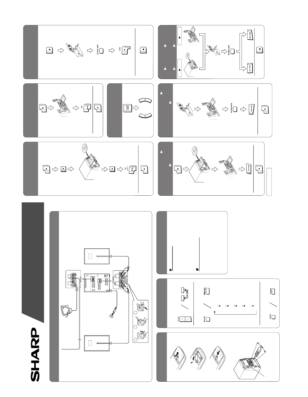
Connect the AC power cord to the AC outlet, and press the RESET
button once on the rear of the main unit.
When the RESET button is pressed, all of the contents in memory
(clock and timer settings, and CD presets) other than the tuner sta-
tions will be erased.
If strange sounds, smells or smoke come out of the unit or if a foreign
object falls into the unit, turn off the power, unplug the AC power
cord from the AC outlet, immediately. Contact the shop where you
purchased the unit.
(Continued)
When an error message is displayed, proceed as follows:
Error messages
Meaning
Remedy
BLANK MD
Nothing is recorded.
Replace it with another disc.
Can't COPY
You tried to record from a copy-protected disc.
Replace it with a regular disc that can be copied.
Can't EDIT
A track cannot be edited.
Change the stop position of the track and then try editing
it.
Can't REC
Recording cannot be performed correctly due to vibra-
tion or shock in the unit.
Re-record.
Can't T REC
Timer recording is impossible or there is no available
space on the MD.
Replace it with another disc.
CH ERROR
There is something wrong with the CD changer.
Set this unit to the stand-by mode and then back to on,
and press the button.
CONNECT ERR
While an MD player is being edited on this unit, incorrect
digital signals are input from the portable MD player.
Make sure the cable is connected correctly and that
power is being supplied to the portable MD player.
DEFECT
Since this disc has scratches on it, the recording opera-
tion was skipped.
Replace it with another disc.
Din UNLOCK
Incorrect digital signals are input.
Connect correct digital signals.
Use the analog input jacks.
DISC ERR
The disc is damaged.
A TOC is not written on the MD or there is something
wrong with data.
Reload the disc or replace it.
DISC FULL
The disc is out of recording space.
Replace the disc with another recordable disc.
EDIT OVER
There is no space to make CD editing on the disc.
Replace it with a disc that has enough time to record.
FOCUS ERROR
A disc has not been loaded.
The disc data cannot be read.
Reload the MiniDisc.
MD ERROR
No operation.
Contact the shop where you purchased the unit.
MECHA ERR∗
(∗:Number or
symbol)
There is a mechanical problem and the disc is not work-
ing properly.
Set this unit to the stand-by mode and press the but-
ton.
NAME FULL
The number of characters for the disc name or track
name exceeds 100.
Shorten the disc or track name.
NO DISC
A disc has not been loaded.
The disc data cannot be read.
Load a disc.
Reload the disc.
NOT AUDIO
The data recorded on this disc is not audio data.
Select another track.
Replace the disc.
PLAYBACK MD
You tried to record on a playback-only disc.
Replace it with another recordable disc.
PROTECT
Trouble is found.
Restart the unit. I f the unit doesn't work, contact a
SHARP Authorized Servicing Dealer or SHARP
Authorized Service station.
PROTECTED
The disc is write protected.
The tape is protected against accidental erasure.
Move the write protection tab back to its original position.
Cover the accidental erase prevention hole.
TAPE ERROR
The tape mechanism is defective.
Try pressing the RESET button.
TEMP OVER
The temperature is too high.
Set this unit to the stand-by mode and wait for a while.
TOC ERR∗
(∗:Number or
symbol)
The disc is damaged.
TOC information cannot be read.
MD not specified.
Replace it with another disc.
TOC FULL∗
(∗:Number or
symbol)
There is no space left for recording character information
(track names, disc names, etc.).
Replace it with another recordable disc.
TOC W ERROR
Recording is impossible.
Contact the shop where you purchased the unit.
TRAY ERROR
The CD tray operates incorrectly.
Unplug the AC power cord, plug it back, and then turn
the power on.
U TOC ERR∗
(∗:Symbol)
TOC information recorded on the MD does not match
the MD specifications or it cannot be read.
Replace it with another disc.
Erase all of the track, and try recording.
U TOC W ERR
The TOC information could not be created properly due
to a mechanical shock or to scratches on the disc.
Turn off the power, and try to write the TOC again.
(Remove any source of shock or vibration while writing.)
? DISC
The data contains an error.
Replace it with another disc.
00:00
Music is not being recorded.
Replace the disc with another recordable disc.
– 7 –
Page 8
MD-X60
MD / CD COMPONENT
SYSTEM
MD-X60
Quick-Guide
Guía rápida
Conexión
Connection
Remote control
Controlador remoto
1
2 3
FM Antenna
Antena de FM
AM Loop Antenna
Antena de cuadro de AM
Right Speaker
Altavoz derecho
Left Speaker
Altavoz izquierdo
AC 120V, 60Hz
120V CA, 60Hz
15
15
The sound level at a given volume setting
depends on a combination of speaker efficiency,
location and various other factors. It is advisable
to avoid exposure to high volume levels, which
can occur while turning the unit on with the
volume control setting up high, or while continu-
ally listening at high volume levels.
El nivel de sonido en una posición de volumen
fijado depende de una combinación del
rendimiento de las altavoces, la posición y varios
otros factores. Es aconsejable evitar un aumento
de volumen. Esto se produce, por ejemplo, al
conectar el aparato con el volumen puesto en
una posición alta. Evite continuar la audición
prolongada a altos niveles de sonido.
Volume setting
Ajuste del volumen
Precaution
Precaución
Volume control
Control del volumen
Volume
Extra-BASS
Graves extra
Remote sensor
Sensor remoto
Connecte el cable negro al terminal negativo (-), y el
cable rojo al terminal positivo (+).
Connect the black wire to the minus (-) terminal, and
the red wire to the plus (+) terminal.
Pre-programmed equalizer
Volumen
Ecualizador preprogramado
8" - 20' (0.2 m - 6 m)
0,2 m - 6 m
2 "AA" batteries
Dos pilas "AA"
FLAT
HEAVY-2
HEAVY-1
SOFT-1
SOFT-2
VOCAL
To an AC outlet
A un tomacorriente de CA
CD playback
Reproducción de
discos compactos
Reproducción de un
minidisco
Playing a MiniDisc
Tape playback
Reproducción de cintas
TINSZ0338AWZZ
Etiqueta hacia arriba.
Label facing up.
Funcionamiento de la
radio
Radio operation
Edición con una
pulsación
(CD
MD)
One-touch editing
(CD MD)
One-touch editing
(TAPE
MD)
Edición con una
pulsación
(TAPE
MD)
Edición con una pulsación
(CD
TAPE) (MD
TAPE)
CD TAPE
Printed in Malaysia
Impreso en Malaysia
A9805.YO
(CD)
(CD)
(CD)
(CD)
(CD)
(MD)
(MD)
(MD)
(CD)
(CD)
(MD)
(TAPE)
(TAPE)
(TAPE)
One-touch editing
(CD TAPE) (MD
TAPE)
(TAPE)
MD TAPE
QUICK GUIDE
– 8 –
Page 9
DISASSEMBLY
(A1) x5
ø3 x8mm
(A1) x2
ø3 x8mm
(A1) x2
ø3 x8mm
(B1) x3
ø3 x8mm
(B1) x11
ø3 x8mm
Cabinet
Front Panel
Rear Panel
(Upper)
Rear Panel
(Bottom)
MD-X60
Caution on Disassembly
The disassembling the machine or assembling it after
repair, observe the following instructions so as to ensure
safety and keep its performance.
1. Unload the compact disc, and mini-disc, casette tape
from machine.
2. Be sure to unplug the power cable before starting
disasembly of the machine.
3. When disassembling each section, remove the nylon
band or wire arrangement.
After servicing the unit, be sure to rearrange the leads
where they were before disassembling.
If a screw of improper length is fit to the MD mechanism.
(a screw fit the part to the mechanism chassis of MD
section), it may contact the optical pickup, impeding
normal operation. Hence, due care must be taken.
4. While repairing, pay utmost attention to static electricity
on ICs.
MAIN UNIT
STEP REMOVAL PROCEDURE FIGURE
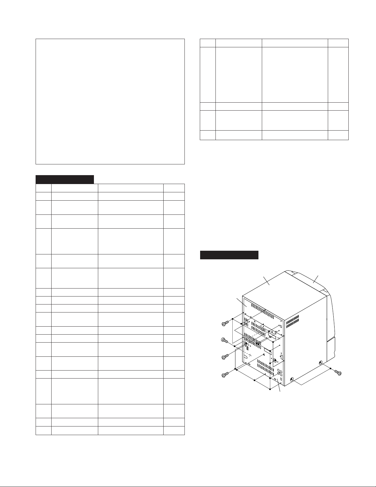
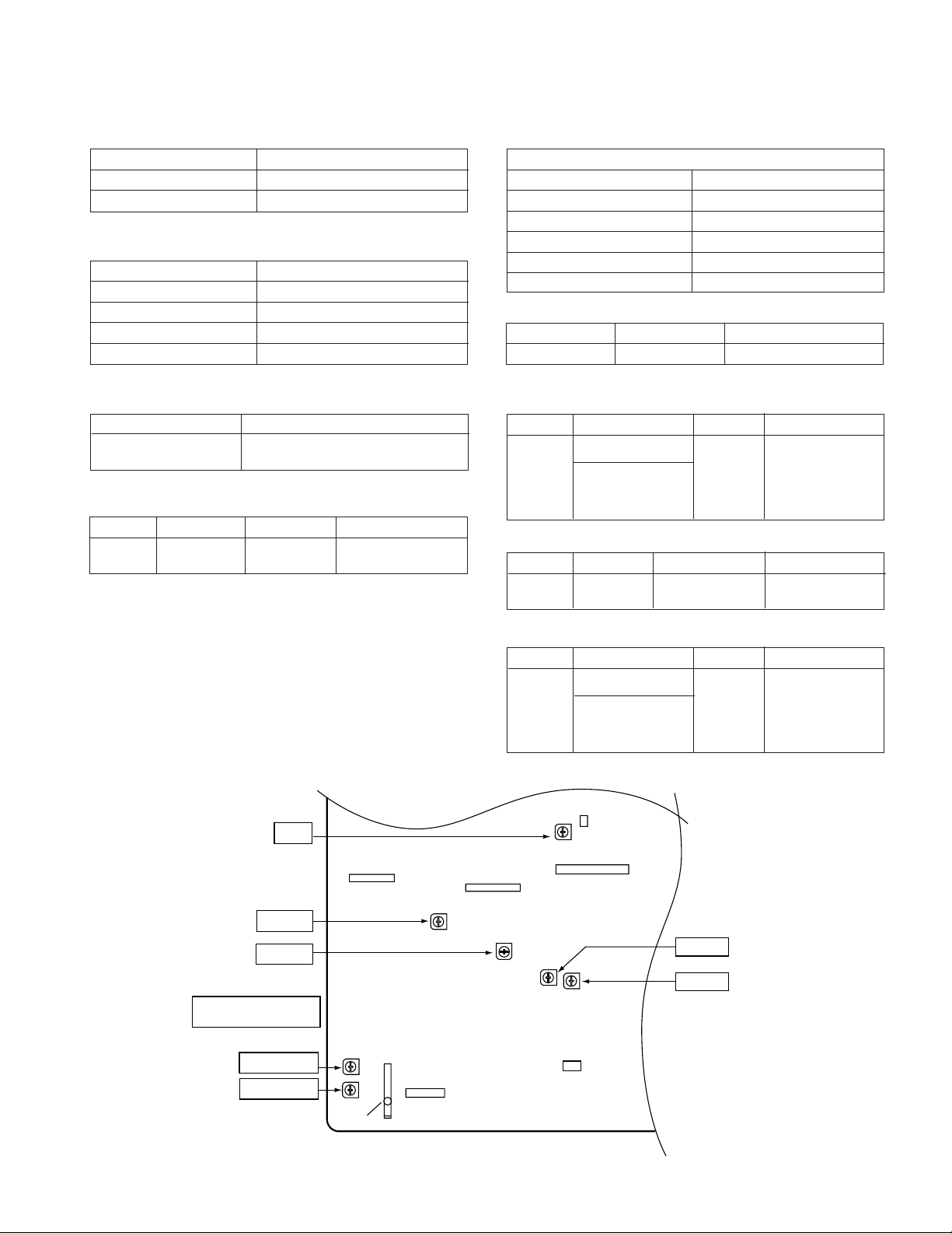
1 Cabinet 1. Screw ................ (A1) x9 9-1
2 Rear Panel 1. Screw ................ (B1) x14 9-1
(Upper,Bottom)
3 CD Changer Block 1. Screw ................ (C1) x6 10-1
4 Main PWB 1. Screw ................ (D1) x3 10-1
5 Fan Motor 1. Socket ............... (E1) x1 10-2
6 Power Amp. PWB 1. Socket ............... (F1) x2 10-2
7 Fuse PWB 1. Screw ................ (G1) x2 10-2
8 MD Holder 1. Screw ................ (H1) x4 10-2,3
9 MD Unit 1. Screw ................ (J1) x2 10-3
10 Front Panel 1. Socket ............... (K1) x1 10-4
11 Power PWB 1. Screw ................ (L1) x5 10-4
12 Tape Mechanism 1. Screw ................ (M1) x4 10-5
13 Tray Switch PWB 1. Screw ................ (N1) x2 10-5
14 Display PWB 1. Screw ................ (P1) x9 10-5
15 Switch A PWB 1. Screw ................ (Q1) x2 10-5
16 Switch B PWB 1. Knob.................. (R1) x1 10-5
17 Jack PWB 1. Socket ............... (S1) x1 10-5
18 Level Volume PWB 1. Screw ................ (T1) x1 10-5
19 Headphone PWB 1. Screw ................ (U1) x1 10-5
2. Screw ................ (C2) x2
2. Socket ............... (D2) x6
3. Flat Cable.......... (D3) x3
4. Socket ............... (D4) x2
2. Screw ................ (E2) x2
2. Lug Wire............ (F2) x1
3. Screw ................ (F3) x3
2. Screw ................ (K2) x5
2. Socket ............... (N2) x1
2. Flat Cable.......... (P2) x1
2. Nut..................... (R2) x1
3. Screw ................ (R3) x5
4. Screw ................ (R4) x1
2. Screw ................ (S2) x1
STEP REMOVAL PROCEDURE FIGURE
20 CD Mechanism 1. Screw ................ (V1) x7 11-1
21 MD Mechanism 1. Screw ................ (W1) x8 11-2
22 MD Main PWB 1. Screw ................ (X1) x4 11-3
(Note 1 ) 2. Socket ............... (X2) x5
23 MD Mechanism 1. Screw ................ (Y1) x4 12-1
2. Top Bord ........... (V2) x1
3. Disc Holder ....... (V3) x1
4. Disc Tray ........... (V4) x3
5. Screw ................ (V5) x3
6. Mechanism Holder
Guide................. (V6) x1
7.
Mechanism Holder
8. Screw ................ (V8) x4
3. Flat Cable.......... (X3) x1
(V7) x1
Cares after repairing
After completion of repair of product set the following shipping
mode to return.
1. Make sure that there is no CD disc, and then press the VOLUP/CD DISC1 PLAY button to turn on the power, and set the
TEST mode.
2. After the indication of TEST END appears, unplug the power
cord. If this test mode is executed, the data stored by the
user in the preset memory are all cleared. It is necessary
tell and obtain the consent of user in advance.
MAIN UNIT
Figure 9-1
Note 1: After removing the connector for the optical pickup
from the connector wrap the conductive aluminium foil
around the front end of connector so as to protect the
optical pickup from electrostatic damage.
– 9 –
Page 10
MD-X60
CD Chenger
Block
(C1) x6
(C2) x2
ø3 x10mm
Front Panel
(D3) x1
Pull
Pull
(D3) x2
Pull
(J1) x1
ø1.7 x3mm
(H1) x1
ø3 x10mm
MD Holder
(J1) x1
ø3 x10mm
Front Panel
(D2) x6
Main PWB
Fuse PWB
(G2) x2
ø3 x10mm
(F1) x1
(F3) x2
ø3 x12mm
Power Amp.
PWB
Fan Motor
(H1) x1
ø3 x10mm
(D4) x2
(E2) x2
ø3 x10mm
(F3) x1
ø3 x10mm
Figure 10-1
(D1) x2
ø3 x10mm
Front Panel
(E1) x1
(F1) x1
Pull
(D1) x1
ø3 x10mm
(F2) x1
Lug wire
MD Unit
MD Holder
(H1) x2
ø3 x10mm
(L1) x1
ø3 x8mm
(L1) x4
ø4 x8mm
Power PWB
Pull
Figure 10-3
(K2) x2
ø3 x10mm
MD Unit
Front Panel
(K1) x1
Pull
(K2) x3
ø3 x8mm
Figure 10-2
Tray Switch PWB
Switch B PWB
(R4) x1
ø3 x8mm
Headphone PWB
(N1) x2
ø3 x10mm
(R3) x5
ø3 x10mm
(U1) x1
ø3 x10mm
(N2) x1
(P1) x9
ø3 x10mm
(M1) x4
ø3 x10mm
(Q1) x2
ø3 x10mm
Display PWB
(T1) x1
ø3 x10mm
Lug Wire
Figure 10-5
Front Panel
Washer
(S2) x1
ø3 x10mm
(R1) x1
(R2) x1
Pull
(P2) x1
Pull
Switch A PWB
Tape Mechanism
Leve Volume PWB
Jack PWB
(S1) x1
Figure 10-4
– 10 –
Page 11
MD-X60
(X3)x1
(X2)x1
(X2)x3
(X2)x1
(X1)x4
ø1.7 x 3mm
MD Main PWB
Pull
(W4) x1
Chassis
Optical pickup
Flexible PWB
(Note 1)
(Note 1) After removing the flexible PWB for optical pickup
from the connector wrap the front end of flexible PWB in
conductive aluminum foil so as to protect the optical pickup
from being damaged electrostatically.
(V1) x2
ø2 x7mm
(V5) x2
ø2 x6mm
Disc Tray 1
Spring
(V2) x1
(V3) x1
(V5) x1
ø2.6 x12mm
(V6) x1
(V7) x1
.
Push
Pawl
CD
Mechanism
(V8) x4
ø2.6 x10mm
(V1) x1
ø3 x10mm
(V1) x2
ø3 x8mm
Turn clockwise the
main cam to raise the
CD mechanism up to
the uppermost position.
PWB-B8
(W1) x 1
ø2 x 4mm
(W1) x 1
ø3 x 10mm
MD Unit
MD Holder
(V4) x3
Disc Tray 2
Disc Tray 3
shield Case(Upper)
(W1) x 1
ø2 x 4mm
(W1) x 1
ø3 x 10mm
(W1) x 1
ø2 x 4mm
MD Holder
(V1) x2
ø3 x10mm
Bracket
(W1) x 1
ø3 x 10mm
Figure 11-1
Press in turns the arrow
1
parts, starting with the
2
uppermost one, to
3
withdraw the disc trays
(W1) x 1
ø2 x 4mm
shield Case(Below)
Figure 11-2
(W1) x 1
ø3 x 10mm
Figure 11-3
– 11 –
Page 12
MD-X60
MD Mechanism
(Y1)x4
ø1.7x8.9mm
Figure 12-1
SPEAKER
STEP REMOVAL PROCEDURE FIGURE
1 Speaker 1. Net ..................... (A1) x9 12-2
2. Front Panel ....... (A2) x9
3. Screw ................ (A3) x9 12-3
SPEAKER
Front Panel
( A2 ) x1
Super Tweeter
Super Tweeter
Front Panel
( A3 ) x2
ø3x10mm
Net
( A1 ) x1
Tweeter
Figure 12-2
Woofer
– 12 –
Tweeter
( A3 ) x1
ø3x6mm
( A3 ) x3
ø3x8mm
( A3 ) x4
ø4x16mm
Woofer
Figure 12-3
Page 13
REMOVING AND REINSTALLING THE MAIN P ARTS
Slider Lever
Cartridge Holder
Clampa Lever
Lack Gear
Roller Arm Lever
Loading Motor
Cam Plate Lever
(B1) x1
Ø1.7x5mm
(B2) x1
Holder Arm
MD-X60
MD MECHANISM SECTION
Perform steps 1 to 9,21 and 23 of the disassembly method to
remove the MD mechanism.(Refering to p.9~12)
How to remove the magnetic head
(See Fig. 13-1)
1. Remove the screws (A1) x 1 pc.
Caution:
Take utmost care so that the magnetic head is not damaged
when it is mounted.
How to remove the cartridge holder
(See Fig. 13-2)
1. Open the rpller arm lever in the arrow direction, and lower
the clamper lever to the rear side.
2. Apply +5V to the red line side of blue connector of loading
motor, push the rack gear in the arrow direction to move the
cam plate lever until tick is heard.
3. Remove the screw (B1) x1 pc., and the spring (B2) x1 pc.,
fitted to the holder arm, and shift the cartridge holder to the
left side to remove it.
(A1)x1
ø1.7x5mm
Magnetic Head
MD Mechanism
Figure 13-1
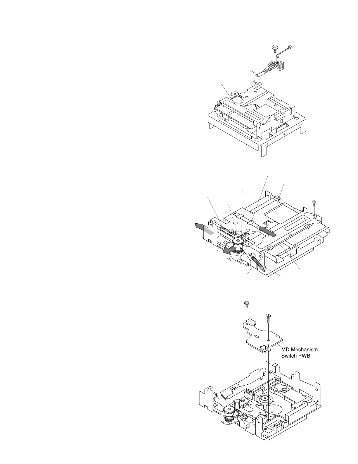
How to remove the mechanism switch PWB
(See Fig. 13-3)
1. Remove the screws (C1) x 2 pcs., and remove the mechanism
switch PWB.
Figure 13-2
(C1)x1
Ø1.7x3mm
(C1)x1
Ø1.7x9.5mm
Figure 13-3
– 13 –
Page 14
MD-X60
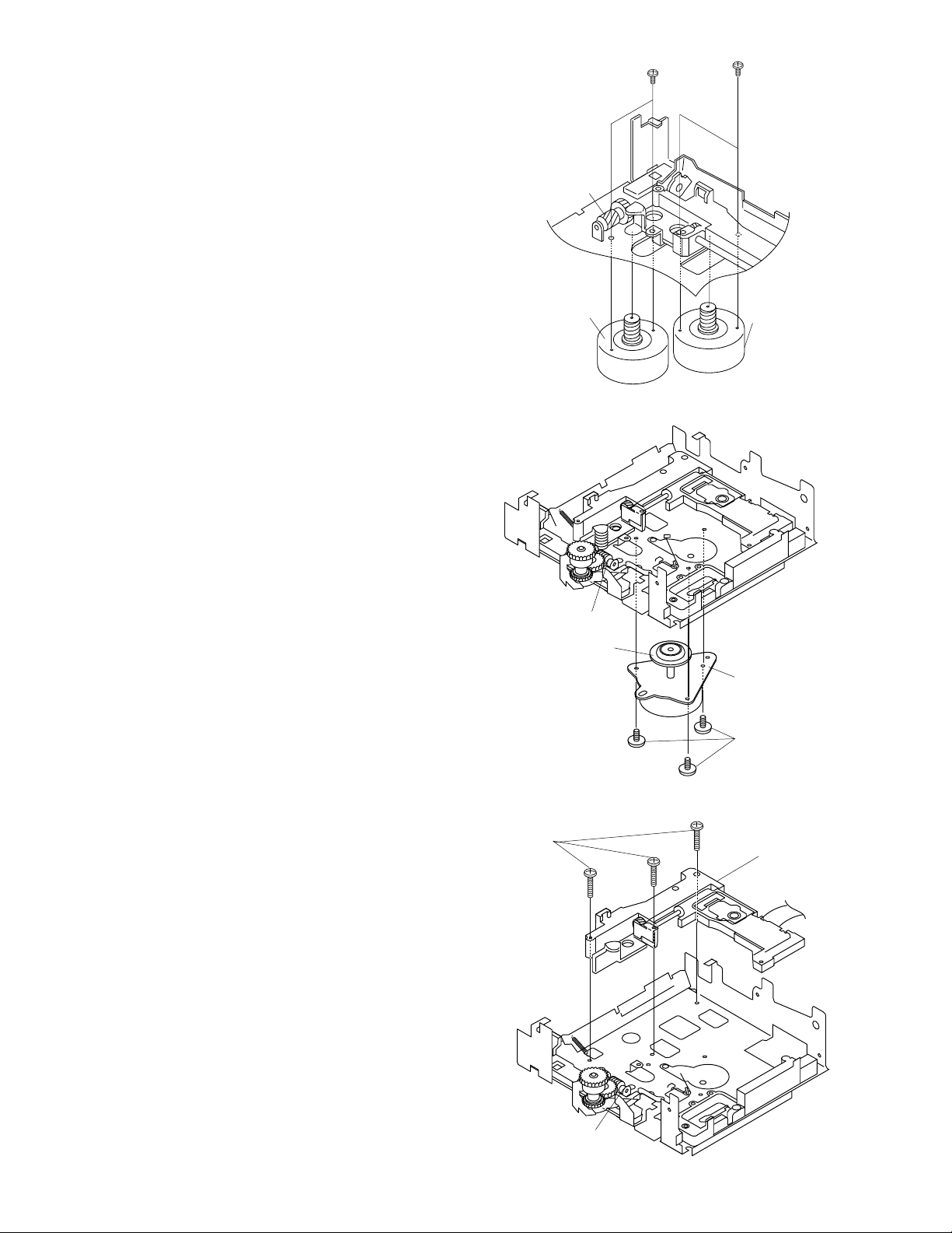
How to remove the sled motor/loading motor
(See Fig. 14-1)
1. Remove the screws (D1) x 4 pcs., and remove the sled
motor/loading motor.
Caution:
Be careful so that the gear is not damaged.
(The damaged gear emits noise during searching.)
How to remove the spindle motor
(See Fig. 14-2)
1. Remove the screws (E1) x 3 pcs., and remove the spidle
motor.
(D1)x2
Ø1.7x2mm
Gear
Loading
Motor
(D1)x2
Ø1.7x2mm
Sled
Motor
Figure 14-1
Caution:
Be careful so that the turntable is not damaged.
How to remove the optical pickup
(See Fig. 14-3)
1. Remove the screws (F1) x 3 pcs.
Caution:
Be careful so that the gear is not damaged.
(The damaged gear emits noise during searching.)
Gear
Turntable
Spindle Motor
(E1)x3
Ø1.7x2.5mm
Figure 14-2
(F1)x3
Ø1.7x9.5mm
Optical Pickup
– 14 –
Gear
Figure 14-3
Page 15
MD-X60
CD MECHANISM SECTION
For the procedure to remove the CD mechanism from the
main unit, refer to Disassembling Procedure, Steps 1~3, and
20. (p.9~11).
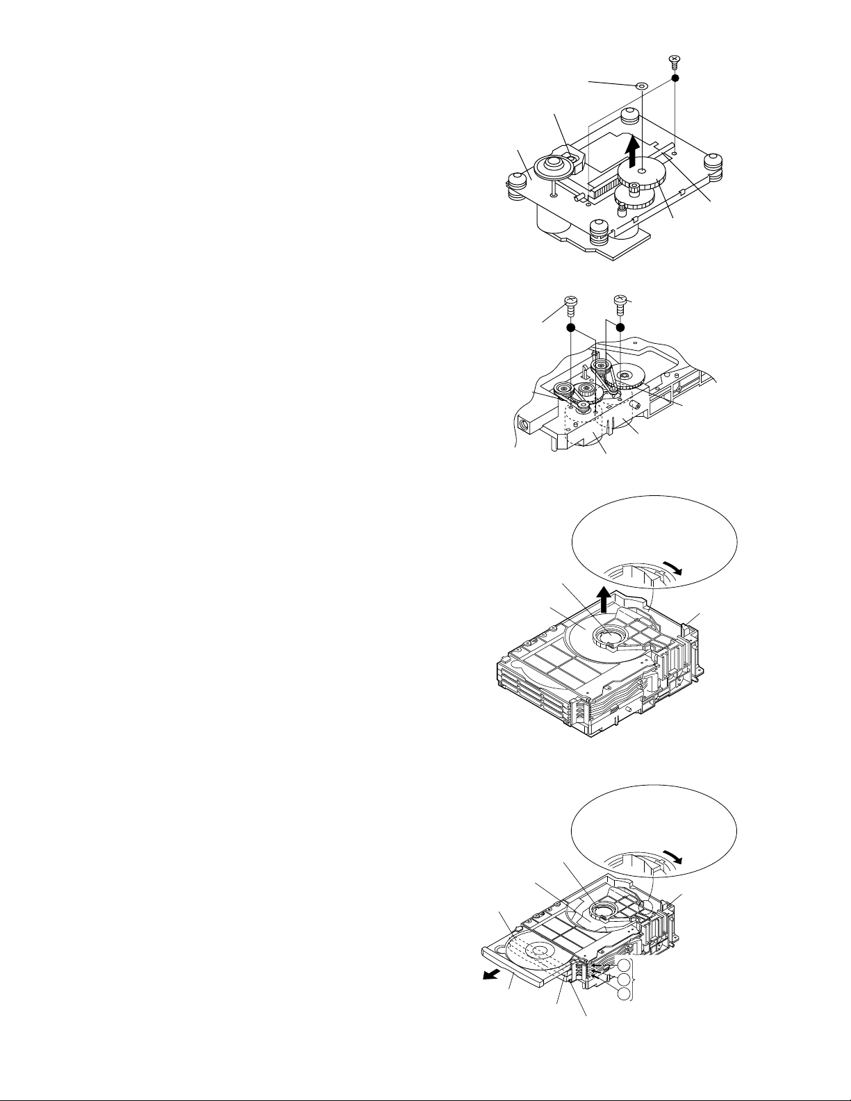
How to Remove the optical pickup
(See Fig. 15-1.)
1. Remove the screws (A1)x 2 pcs., to remove shaft (A2)x 1
pc.
2. Remove stop washer (A3)x 1 pc., to remove gear (A4)x 1 pc.
3. Remove the optical pickup.
Note:
After disconnecting the optical pickup connector wrap the
front end of connector in conductive aluminum foil so as to
prevent damage to the optical pickup by static electricity.
How to Remove the tray motor/main cam motor
(See Fig. 15-2.)
1. Remove the CD changer section by the method described
in page 8, and disassemble as shown in the figure.
2. Remove the belts (B1)x 2 pcs., from the motor side.
3. Remove the screws (B2)x 4 pcs.
4. Remove the tray motor and main cam motor.
Stop Washer
(A3) x1
Pickup
CD
Mechanism
(B2) x2
ø2.6 x4mm
Belt
(B1) x1
(A1) x2
ø2.6 x5mm
Figure 15-1
(B2) x2
ø2.6 x4mm
Main Cam
Motor
Tray Motor
Figure 15-2
Gear
(A4) x1
Belt
(B1) x1
Shaft
(A2) x1
How to remove the CD disc
(When CD is in playback state)
(See Fig. 15-3.)
1. Remove the cabinet and front panel.
2. Disassemble as shown in the figure so that the CD disc of
CD changer becomes visible.
3. Remove the CD disc as shown in the figure.
How to remove the CD disc
(When CD exists in the tray)
(See Fig. 15-4.)
1. Remove the cabinet and front panel.
2. Disassemble as shown in the figure so that the CD disc of
CD changer can be taken out.
3. Remove the CD disc from the tray as shown in the figure.
Turn the main cam clockwise,
and raise the CD mechanism
and disc holder up to
uppermost position.
Disc Holder
CD Disc
(When CD is in playback state.)
Figure 15-3
Turn the main cam clockwise,
and raise the CD mechanism
and disc holder up to
Disc Holder
CD Mechanism
CD Disc
uppermost position.
CD Changer
Block
CD Changer
Block
– 15 –
Disc Tray 1
Disc Tray
Press in turns the arrow
1
parts, starting with the
2
uppermost one, to
3
2
Disc Tray
withdraw the disc trays
3
(When CD exists in the tray.)
Figure 15-4
Page 16
MD-X60
ADJUSTMENT
TUNER SECTION
fL: Low-range frequency
fH: High-renge frequency
• AM adjustment and confirmation
AM signal oscillator Frequency 400 Hz, 30%, AM modulation
Adjusting item Adjusting object
IF Adjust the indication of Set IF wafeform
T351 set to 1,720 kHz.
Frequency cover fL: T306 (530 kHz) fL: 1.1 ± 0.1 V
(VT line voltage of Adjust the indication fH: 5.1 ± 1.3 V of
pin 20 of IC302) of set to 522 kHz. (Only confirmation)
Tracking fL: T302 (990 kHz) Set the output of
• FM mute level adjustment
FM signal oscillator Frequency 400 Hz, 22.5 kHz
Frequency Adjusting
98 MHz 30 dB VR351 Input: SO301
Adjusting
method
object
Adjusting
method
450 kHz to maximum.
speaker terminal
to maximum.
Adjusting object
Output: Speaker
Terminal
• TEST mode setting method
Holding down the ENTER button and TUNER (BAND) button,
turn on the power. Frequency is set in the memory (initial
setting) as shown in Table 16. Call the setting with the
PRESET button to use it for tuner circuit adjustment or
confirmation.
Preset No. Frequency
P01 87.5 MHz P06 530 kHz
P02 108.0 MHz P07 1,720 kHz
P03 90.0 MHz P08 600 kHz
P04 106.0 MHz P09 1,400 kHz
P05 98.0 MHz P10 990 kHz
Preset No. Frequency
Table 16 Initial setting of memory
• Erasing the registered broadcast station
Holding down TRACK EDIT and ENTER in power-off state,
press POWER.
All the registered stations are erased.
Note:
Even when the RESET switch provided at the rear side of this
model, is pressed, the preset of tuner is not cleared.
AM Loop Antenna
FM signal oscillator
IF : Speaker Terminal
Freqency cover: IC302,Pin 20
Loop Antenna
Figure 16-1 AM IF
UNIT
GND
T302
AM Tracking
Electronic
voltmeter
T306
FM signal oscillator
TUNER PWB
T351
AM IF
VR351
FM Mute Level
AM Band Coverge
FE301
20
SO301
Figure 16-2 FM Mute Level
1213
IC302
1
UNIT
Speaker
Terminal
Electronic
voltmeter
SO301
Antenna Terminal
Figure 16-3 Adjustment Point
– 16 –
Page 17
TAPE SECTION
MD-X60
Adjusting the mechanism
Driving Force Check
Torque Meter Specified Value
Play:TW-2412 120 g or more
Reverse Play:TW-2422 120 g or more
Checking the playback/FF/rewinding torque
Torque Meter Specified Value
Play:TW-2111 25 to 65 g.cm
Reverse Play:TW-2121 25 to 6 5 g.cm
Fast forward:TW-2231 60 to 130 g.cm
Rewind:TW-2231 60 to 130 g.cm
Adjusting the record / playback head azimuth
Test Tape
MTT-114 Output: L:TP102 pin 3
Tape Speed
Test Tape
MTT-111 VR107 3,000±30Hz L:TP102 pin 3
* Raise the cassette holder cover and remove it, and then
adjust the azimuth.
Adjusting Point
Instrument Connection
R:TP102 pin 1
Specified Value
Instrument Connection
R:TP102 pin 1
Adjusting the deck circuit
Position of each swich or control
VOLUME MAX
FUNCTION TAPE
TAPE NORMAL
DOLBY NR OFF
REVERSE MODE NORMAL
BEAT SW A
Checking the bias oscillation Frequency
Adjusting Point Specified Value
- 102±7kHz TP101(IC102 pin 3)
Adjusting the record/playback frequency
Test Tape
UR-121 L:VR101 10mV Output
Adjusting Point
Record level control
R:VR102 L:TP102 pin 3
Adjusting the playback amplifier sensitivity
Test Tape
Adjusting Point
MTT-150 L:VR103 Standard:300mV L:TP102 pin 3
R:VR104 R:TP102 pin 1
Specified Value
Instrument Connection
Specified Value
10mV Input:AUX
Instrument Connection
(10kHz)
R:TP102 pin 1
Instrument Connection
TAPE
SPEED
R-CH
PLAY SENS.
L-CH
PLAY SENS.
MAIN PWB
L-CH
REC FREQUENCY
R-CH
REC FREQUENCY
VR101
VR102
TP101
CNP930
IC102
3
VR104
CNP101
Adjusting the record/playback sensitivity
Test Tape
UR-121 L:VR105 100mV Output
VR107
CNP102
VR103
VR105
Adjusting Point
Record level control
Specified Value
100mV Input:AUX
R:VR106 L:TP102 pin 3
CNP103
CNP920
L-CH
REC SENS.
R-CH
VR106
TP102
2
1
3
Pin 1 : R
Pin 3 : L
REC SENS.
Instrument Connection
(1kHz)
R:TP102 pin 1
Figure 17 Adjustment Point
– 17 –
Page 18
MD-X60
CD TEST MODE
CD test mode setting
Any one of test mode can be set by pressing several buttons as follows.
Holding down VOL-UP and CD DISC 3 PLAY, turn on POWER. TEST: CD operation test
Test Mode
Function - CD TEST mode
Setting of Test mode
Indication of CD TEST mode
OPEN/CLOSE operation is manual operation.
The pickup can be moved with the (
) or ( ) button.
<CD MD EDIT> <TRACK> <CD-STOP>
Tracking on the spot. Tracking on the spot. STOP
SERVO ON PLAY SERVO OFF PLAY
<PLAY> button input - TOC. Initialization performed, and the ordinary PLAY is performed.
Press the <STOP> button. Stop
If the following button is pressed during PLAY, it is possible to specify directly any Track No.
<Disc 1 PLAY> button: Track 4
<Disc 2 PLAY> button: Track 9
<Disc 3 PLAY> button: Track 15
Note:
Only in STOP state it is possible to slide the pickup with the (
Cancel method: POWER OFF
Initialization is not performed.
) or ( ) button.
CD SECTION
Since this CD system incorporates the following automatic adjusting function, when the pickup is replaced, it is not necessary
to the readjust it .
Since this CD unit does not need adjustment, the combination of PWB and laser pickup unit is not restricted.
Automatic adjustment items
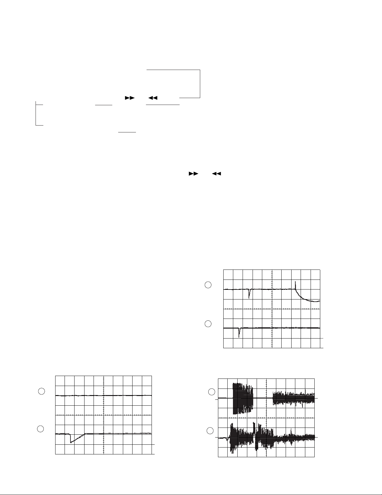
1. Focus Offset (Fig. 18-1)
2. Tracking Offset (Fig. 18-2)
3. E/F Balance (Tracking Error Balance) (Fig. 18-3)
4. R/F level AGC function (HF level: Constant)
5. RF level automatic follow-up of the tracking gain
This automatic adjustment is performed each time a disc
is changed. Therefore, each disc is played back using
the optimal settings.
10ms
0.50 V
IC1 20 FE
Enlarged
View
0.1s
0.50 V
IC1 20 FE
0.1s
0.50 V
IC1 7 TE
200 ms
1V/diV
IC 1 15
TO
Figure 18-1
FOCUS
OFF-SET
ADJUST
TRACKING
OFF-SET
ADJUST
1
2
TRACKING/
ERROR
BARANCE
1
ADJUST
10ms
0.50 V
IC1 7 TE
Figure 18-2
TRACKING
OFF-SET
ADJUST
1
2
– 18 –
200 ms
1V/diV
IC 1 7
TE
2
Figure 18-3
Page 19
MD-X60
MD SECTION
When the combination of mechanism/pickup and PWB was changed , set the TEST mode to perform the AUTO preliminary
adjustment and AUTO adjustment, write the adjustment data in EEPROM.
When EEPROM was replaced, set the TEST mode,write the EEPROM set data (p28,p29) and then perform the preliminary
adjustment and AUTO adjustment, write adjustment data in EEPROM.
1. Preparation for adjustment
Test disc
Type Test disc
1 High reflection disc TGYS1 (SONY) [for Playback] RRCDT0101AFZZ
2 Low reflection disc Recording minidisc UDSKM0001AFZZ
3 Head Adjusting transparent RRCDT0103AFZZ
[TEAC Test MD]
4 Low reflection disc Pre-adjustment disc 88GMMD-318
Extension Cable (See Fig. 19)
Type Part No.
1 Extension PWB for servicing RUNTK0457AFZZ
2 Extension Connector (2 Pin) QCNWK0059AFZZ
3 Extension Connector (6 Pin) QCNWK0107AFZZ
4 Extension Cable (5 Pin) QCNWK0109AFZZ
5 Extension Cable (28 Pin) QCNWK0108AFZZ
Part No.
5Pin extension flat cable
QCNWK0109AFZZ
CN1601(Bottom side)
CN1602
CN1603
CN1604(Bottom side)
MD MAIN PWB
6P-2P extension connector
QCNWK0107AFZZ
CN1252
CN1101
2Pin extension connector
QCNWK0059AFZZ
From
motor
From mechanism switch
PWB
28Pin extension
flat cable
QCNWK0108AFZZ
From Magnetic Head
From Optical
Pickup Unit
Extension PWB for service
(RUNTK0457AFZZ)
Fit the extension PWB for service to the mechanism
Figure 19 Conection of Extention Cable
– 19 –
Page 20
MD-X60
2. Test mode
Test mode setting method
1. Holding down the POLE POSITION button and MD
(State A is changed to state B .)
2. Insert the playback disc 1 (high reflection disc) or recording disc 2 (low reflection disc). (State C is set.)
Thus, the test mode state is set.
(PLAY/PAUSE) button, press the POWER button.
A tsm
TEST STOP state (When the MD
e : TEST MODE represents version of MD microcomputer.
(STOP) button is ressed in the C state, the indication A
is restored. To restore C again, press the CD
(PLAY/ PAUSE)
button.)
B EJECT
TEST
C AUT YOBI
TEST
Entering the specific mode
Whenever the CD
AUTO pre-adjustment AUTO adjustment RESULT Pre-adjustment
(PLAY/PAUSE) button is pressed, the mode is changed.
RESULT
EEPROM setting MANUAL adjustment MANUAL pre-adjustment
Cancel of TEST mode
When the ENTER button is pressed, data is written in EEPROM, and then the TEST mode is canceled. (Mode where automatic
adjustment is not performed)
To restore the usual state once reset.
When the data of EEPROM was changed or the preliminary adjustment was performed again, be sure to press the ENTER
button to write data in the EEPROM.
(Data is written in the EEPROM by pressing the ENTER button.)
* Be sure to ascertain "COMPLETION" by pressing the MD PLAY button in the AUTO preliminary adjustment mode before
pressing the ENTER button.
• Test Mode
1. EJECT mode • TEMP setting (of EEPROM setting)
• CONTROL setting (of EEPROM setting)
• Setting of laser power (record/playback power)
2. AUTO pre-adjustment mode • Automatic pre-adjustment is performed. (After adjustment the grating adjustment mode is set.)
• The adjustment value is output with the aid of system controller interface.
3. AUTO adjustment mode • Automatic adjustment is performed.
• The adjustment value is output with the aid of system controller interface.
• Continuous playback is performed. (Error rate indication, jump test)
• RESULT sub-mode •
• RESULT mode (final adjustment)
• MANUAL pre-adjustment mode
• MANUAL adjustment mode
4. EEPROM setting mode • Various coefficients of digital servo are changed manually.
5. TEST-PLAY mode • Continuous playback from the specified address is performed.
6. TEST-REC mode • Continuous recording from the specified address is performed.
7. INNER mode • The position where the INNER switch is turned on is measured.
Because the data of ROM is rewritten in this mode, set malfunction may occur. Therefore do
not set this mode since it is not necessary for the service.
• C1 error rate measurement, ADIP error rate measurement.
– 20 –
Page 21
MD-X60
1. EJECT mode
Step No.
Step 1 Testmode EJECT state [ _ _ E J E C T _ _ _ ]
Step 2 Press oncethe CD STOP button. Max. power output state [ x p w _ _ _ _ _ _ _ ]
Step 3 Press once the CD STOP button. Record power output state [ r p w _ _ _ _ _ _ _ ]
Step 4 Press once the CD STOP button. Playback power output state [ p p w _ _ _ _ _ _ _ ]
Step 5 Press the CD MD EDIT button. TEMP setting of EEPROM setting
Step 6 Press the TRACK EDIT button. CONTROL setting of EEPROM setting
Confirmation of pickup laser power
It is possible to confirm in the record/playback mode with the aid of laser power meter. However, since the laser power meter
measurement is characterized with dispersion, obtained data are used only for confirmation.
Reference data (at room temperature 25°C)
Playback: 0.72±0.1 mV
Record: 5±1 mV
Note: Never see directly the laser light. Otherwise your eyes are injured.
2. AUTO pre-adjustment mode (Low reflection disc only)
With the pre-adjustment disc (MMD-318)
Step No. Setting Method Display
Step 1 Testmode STOP state [ t s m e ]
Step 2 Press once the CD PLAY button. AUTO pre-adjustment menu [ _ A U T _ Y O B I _ ]
Step 3 Press once the MD PLAY button. The slide moves to the innermost periphery, and automatic [ : _ _ _ _ _ _ ]
End of adjustment If adjustment is OK, Step 4.
Step 4 Grating adjustment, [ _ C O M P L E T E _ ]
adjustment value output
Press once the MD STOP button. STEP 2
Step 5 Adjustment value output [ C a n ' t _ A D J . ]
Press once the MD STOP button. STEP 2 AUTO pre-adjustment menu
• : Adjustment name
Setting Method
Remarks Display
(Refer to TEMP setting of EEPROM)
(Refer to CONTROL setting of EEPROM)
Remarks
pre-adjustment is started.
• During automatic adjustment changes as follows.
HAo→ • • • • • • • • • →LAO
If adjustment is NG, Step 5.
3. AUTO adjustment mode
Step No. Setting Method Remarks Display
Step 1 Testmode STOP state [ t s m e ]
Step 2
Step 3 Press once the MD PLAY button. The slide moves to the innermost periphery, and automatic [ : _ _ _ _ _ _ ]
Step 4 Adjustment value output For grating adjustment [ _ C O M P L E T E _ ]
Step 5 Continuous playback (pit section) Comfirmation of CI error [ s c ]
Step 6 Press the CD STOP button. Comfirmation of ADP error [ a a ]
Step 7 Adjustment value output [ C a n ' t _ A D J . ]
Press the CD PLAY button two times.
End of adjustment If adjustment is OK, Step 4.
Press the MD PLAY button. STEP 5
Press the MD STOP button. STEP 2
Continuous playback (groove section)
Press the MD STOP button. STEP 2 AUTO adjustment menu
Press the MD STOP button. STEP 2 AUTO adjustment menu
AUTO adjustment menu [ A U T O _ A J S T _ ]
adjustment is started.
• In case of high reflection disc changes as follows.
PEG→HAG
•In case of low reflection disc changes as follows.
PEG→LAG→GCG→GEG→LAG
If adjustment is NG, Step 7.
[ a c ]
• : Adjustment name, : Measurement value, : Address
– 21 –
Page 22
MD-X60
4. EEPROM setting mode
a) Focus setting
Step No.
Step 1 Testmode STOP state [ t s m e ]
Step 2
Step 3 Press once the MD PLAY button. [ _ _ F o c u s _ _ _ ]
Step 4 Press once the MD PLAY button. [ F G _ _ _ _ _ _ ]
Step 5 Press once the CD PLAY button. [ F F 1 _ _ _ _ _ ]
Step 6 Press once the CD PLAY button. [ F F 2 _ _ _ _ _ ]
Step 7 Press once the CD PLAY button. [ F Z H L E V _ _ ]
Step 8 Press once the CD PLAY button. [ F O K L E V n _ ]
Step 9 Press once the CD PLAY button. [ F O K L E V f _ ]
Step 10 Press once the CD PLAY button. [ F O K L P F n _ ]
Step 11 Press once the CD PLAY button. [ F O K L P F f _ ]
Step 12 Press once the CD PLAY button. [ W A I T f_ _ _ ]
: Setting value
•
Press the CD PLAY button seventimes.
b) Spindle setting
Step No.
Step 1 Testmode STOP state [ t s m e ]
Step 2
Step 3 Press once the MD PLAY button. [ _ _ F o c u s _ _ _ ]
Step 4 Press once the CD PLAY button. [ _ S p i n d l e _ _ ]
Step 5 Press once the MD PLAY button. [ S P G _ _ _ _ _ ]
Step 6 Press once the CD PLAY button. [ S P G _ i n _ _ ]
Step 7 Press once the CD PLAY button. [ S P G _ m i d _ ]
Step 8 Press once the CD PLAY button. [ S P G _ o u t _ ]
Step 9 Press once the CD PLAY button. [ S P 1 _ _ _ _ _ ]
Step 10 Press once the CD PLAY button. [ S P 2 _ _ _ _ _ ]
Step 11 Press once the CD PLAY button. [ S P 3 _ _ _ _ _ ]
Step 12 Press once the CD PLAY button. [ S P 4 _ _ _ _ _ ]
Step 13 Press once the CD PLAY button. [ S P 5 _ _ _ _ _ ]
Step 14 Press once the CD PLAY button. [ S P D L I M _ _ ]
• : Setting value
Press the CD PLAY button seven times.
Setting Method Display
[E E P R O M _ S E T]
Setting Method
Display
[E E P R O M _ S E T]
c) Tracking setting
Step No.
Step 1 Testmode STOP state [ t s m e ]
Step 2
Step 3 Press once the MD PLAY button. [ _ _ F o c u s _ _ _ ]
Step 4
Step 5 Press once the MD PLAY button. [ T G _ _ _ _ _ _ ]
Step 6 Press once the CD PLAY button. [ T F 1 _ _ _ _ _ ]
Step 7 Press once the CD PLAY button. [ T F 2 _ _ _ _ _ ]
Step 8 Press once the CD PLAY button. [ S V C N T 4 _ _ ]
Step 9 Press once the CD PLAY button. [ T R B L V 0 _ _ ]
Step 10 Press once the CD PLAY button. [ T R B L V t _ _ ]
Step 11 Press once the CD PLAY button. [ T R K L V 0 _ _ ]
Step 12 Press once the CD PLAY button. [ T R K L V t _ _ ]
Step 13 Press once the CD PLAY button. [ T D P W o _ _ _ ]
Step 14 Press once the CD PLAY button. [ T D P W t _ _ _ ]
Press the CD PLAY button seven times.
Press the CD PLAY button two times.
Setting Method Display
[E E P R O M _ S E T]
[ _ T r a c k i n g _ ]
– 22 –
Page 23
c) Tracking setting
Step No. Setting Method
Step 15 Press once the CD PLAY button. [ S L C T 0 _ _ _ ]
Step 16 Press once the CD PLAY button. [ S L C T t _ _ _ ]
Step 17 Press once the CD PLAY button. [ S L C T m _ _ ]
Step 18 Press once the CD PLAY button. [ T C R S C 1 P _ ]
Step 19 Press once the CD PLAY button. [ C O T L V P _ ]
Step 20 Press once the CD PLAY button. [ C O T L V r _ ]
Step 21 Press once the CD PLAY button. [ W A I T m_ _ _ ]
: Setting value
•
Display
d) Slide setting
Step No.
Step 1 Testmode STOP state [ t s m e ]
Step 2
Step 3 Press once the MD PLAY button. [ _ _ F o c u s _ _ _ ]
Step 4
Step 5 Press once the MD PLAY button. [ S L G _ _ _ _ _ ]
Step 6 Press once the CD PLAY button. [ S L 2 _ _ _ _ _ ]
Step 7 Press once the CD PLAY button. [ S L D L I M _ _ ]
Step 8 Press once the CD PLAY button. [ S L D L E V _ _ ]
Step 9 Press once the CD PLAY button. [ S L K L V k _ _ ]
Step 10 Press once the CD PLAY button. [ S L K L V t _ _ ]
Step 11 Press once the CD PLAY button. [ S L K L V m _ _ ]
•
: Setting value
Setting Method
Press the CD PLAY button seven times.
Press the CD PLAY button three times.
[E E P R O M _ S E T]
[ _ _ _ S l e d _ _ _ ]
Display
MD-X60
e) TEMP setting
Step No.
Step 1
Step 2 Press the CD MD EDIT button. [ T E M P _ _ ]
• : Setting value, : Measurement value
EJECT state (or mechanism-less state)
Setting Method
Display
[ _ _ E J E C T _ _ _ ]
f) CONTROL setting
Step No. Setting Method Display
Step 1 Testmode STOP state [ t s m e ]
Step 2
Step 3 Press once the MD PLAY button. [ _ _ F o c u s _ _ _ ]
Step 4
Step 5 Press once the MD PLAY button. [ C O N T R L 1_ ]
Step 6 Press once the CD PLAY button. [ C O N T R L 2_ ]
Step 7 Press once the CD PLAY button. [ S P K L E V m_ ]
Step 8 Press once the CD PLAY button. [ A D J T T M_ _ ]
Step 9 Press once the CD PLAY button. [ H D E Q A D_ _ ]
Step 10 Press once the CD PLAY button. [ L D E Q A D_ _ ]
Step 11 Press once the CD PLAY button. [ G D E Q A D_ _ ]
Step 12 Press once the CD PLAY button. [ H D E Q B C_ _ ]
Step 13 Press once the CD PLAY button. [ L D E Q B C_ _ ]
Step 14 Press once the CD PLAY button. [ G D E Q B C_ _ ]
Step 15 Press once the CD PLAY button. [ H A L S G_ _ _ ]
Step 16 Press once the CD PLAY button. [ L A L S G_ _ _ ]
Step 17 Press once the CD PLAY button. [ G A L S G _ _ ]
Step 18 Press once the CD PLAY button. [ H A L S O F S_ _ ]
Step 19 Press once the CD PLAY button. [ L A L S O F S _ _ ]
Step 20 Press once the CD PLAY button. [ G A L S O F S _ _ ]
• : Setting value
Press the CD PLAY button seven times.
Press the CD PLAY button five times.
[E E P R O M _ S E T]
[ _ C o n t r o l _ _ ]
– 23 –
Page 24
MD-X60
G) ADJUST setting
Step No. Setting Method
Step 1 Testmode STOP state [ t s m e ]
Step 2
Step 3 Press once the MD PLAY button. [ _ _ F o c u s _ _ _ ]
Step 4
Step 5 Press once the MD PLAY button. [ C O K _ _ _ _ _ ]
Step 6 Press once the CD PLAY button. [ F A T _ _ _ _ _ ]
Step 7 Press once the CD PLAY button. [ T A T _ _ _ _ _ ]
Step 8 Press once the CD PLAY button. [ C A T _ _ _ _ _ ]
Step 9 Press once the CD PLAY button. [ F A B _ _ _ _ _ _ ]
Step 10 Press once the CD PLAY button. [ S T R _ _ _ _ _ _ ]
Step 11 Press once the CD PLAY button. [ S F S _ _ _ _ _ _ ]
Step 12 Press once the CD PLAY button. [ S T C _ _ _ _ _ _ ]
: Setting value
•
Press the CD PLAY button seven times.
Press the CD PLAY button six times.
5. TEST-PLAY mode
(For comfirmation of the playback ability at the named address.)
Step No.
Step 1 Testmode STOP state [ t s m e ]
Step 2 Press the CD MD EDIT button. TEST-PLAY menu [ T E S T _ P L A Y _ ]
Step 3 Press once the CD STOP button. ADRES setting (Target address initial value is indicated) [ A D R E S _ 0 0 5 0 ]
Step 4 Continuous playback (pit section) (Address + C1 error indication) [s c ]
Step 5 Press once the CD STOP button. (Address + ADIP error indication) [a a ]
Step 6 Press once the MD STOP button. TEST-PLAY menu [ T E S T _ P L A Y _ ]
• If the MD STOP button is pressed while the TEST-PLAY menu is displayed, TEST mode STOP state is set.
• If the MD PLAY button is pressed while the TEST-PLAY menu is displayed, continuous playback is started from the current pickup position.
• Whenever the CD
0 0 5 0 → 0 3 C 0 → 0 7 0 0 → 0 8 A 0 → 0 0 5 0 → …………
• Whenever the CD STOP button is pressed in the address setting mode, the digit which is changed with - / + changes as follows.
0 0 5 0 → 0 0 5 0 → 0 0 5 0 → 0 0 5 0 → …………
• The digit of address which has been specified with - / + and CD STOP button in the address setting mode is set to +01H/-01H.(0~F)
* If the - / + button is held down, the setting changes continuously with 100 ms cycle.
Setting Method
Press once the MD PLAY button.
Continuous playback (groove section)
Continuous playback (groove section)
MD EDIT button is pressed in the address setting mode, the address changes as follows.
Display
[E E P R O M _ S E T]
[ A D J U S T _ _ _ ]
Remarks
(Address + C1 error indication) [a c ]
Display
6. TEST-REC mode
With recording mini disk (For comfirmation of the playback ability at the named address.)
Step No. Setting Method Remarks Display
Step 1 Testmode STOP state [ t s m e ]
Step 2 Press the CD MD EDIT button. TEST-REC menu [ T E S T _ R E C _ _ ]
Step 3 Press once the CD STOP button. ADRES setting (indication of address initial value) [ a 0 0 5 0 _ p w ]
Step 4 Press once the MD PLAY button.
Step 5 Press once the MD STOP button. TEST-REC menu [ T E S T _ R E C _ _ ]
• If the MD STOP button is pressed while the TEST-PLAY menu is displayed, TEST mode STOP state is set.
• If the MD PLAY button is pressed while the TEST-REC menu is displayed, continuous record is started from the current pickup position.
• Whenever the CD MD EDIT button is pressed in the address setting mode, the address changes as follows.
0 0 5 0 → 0 3 C 0 → 0 7 0 0 → 0 8 A 0 → 0 0 5 0 → …………
• Whenever the CD STOP button is pressed in the address setting mode, the digit which is changed with - / + changes as follows.
0 0 5 0 → 0 0 5 0 → 0 0 5 0 → 0 0 5 0 → …………
• The digit of address which has been specified with - / + and CD STOP button in the address setting mode is set to +01H/-01H.(0~F)
* If the - / + button is held down, the setting changes continuously with 100 ms cycle.
• Be sure to remove since excessive raising results in breakage of the pickup.
While searching, set the search output to "H". To start continuous play,
return it to "L".
Continuous recording
[ a p w ]
– 24 –
Page 25
MD-X60
1
2
3
1
2
3
adjusting
hole
Spindle motor
Check the Lissajou's waveform,
shifting the mounting position with
a screwdriver (to be fitted into the
disc motor adjusting hole).
Spindle Motor
Adjusting hole
7. INNER mode
Step No.
Step 1 Testmode STOP state [ t s m e ]
Step 2 Press the TRACK EDIT button. INNER menu [ _ _ I N N E R _ _ ]
Step 3 Press once the MD PLAY button. INNER switch position measurement [s c ]
Step 4 Press once the MD STOP button. INNER menu [ _ _ I N N E R _ _ ]
• : Adress
Setting Method
Remarks Display
(SUBQ address and C1 error are also indicated.)
Lead-in switch position measurement mode
Insert High reflection test disk (TGYS1)
Note: Adjust the lead-in switch position to FF85 to FFD2.
1. Loosen the screw (A) x 2 pcs. which fix the mechanism switch
PWB.
2. Retighten the screw, pressing the mechanism switch PWB in
the arrow direction, and then measure the lead-in switch
position again.
After position adjustment fix with the two screws (A). (See Fig. 25-1.)
Note: After tightening the two screws on the PWB apply Screw Lock.
Forced rotation of loading motor
While the display indication is test mode STOP state or EJECT state,
the loading motor can be forcibly rotated by press theVOL UP/DOWN
button.
Adjustment of magnetic head mounting position
When the magnetic head and optical pickup have been replaced, be
sure to adjust the mounting position.
For easier adjustment of mounting position move the optical pickup
to the center position, and then adjust the position.
1. Set the adjusting transparent disc 3.
2. Lower the magnetic head up-shift arm with your finger, and raise
the magnetic head.
3. Viewing the set from above, make an adjustment so that the
magnetic head aligns with the optical pickup objective lens.
4. Make sure that there is a clearance as shown in Figure 25-2 and
the magnetic head moves up and down smoothly.
Loosen the
two screws (A).
Mechanism Switch PWB
Magnetic head
Objective lens
Circumferential direction
Lead In Switch
Figure 25-1
Radial direction
Push
Mechanism Adjustment
1. Optical pickup grating inspecting method
43 Pin of IC1101
GND (TP1131)
26 Pin of IC1101
EOUT (TP1133)
25 Pin of IC1101
FOUT (TP1132)
100K
470p
470p
100K
OSILLOSCOPE
GND CH1 CH2
XY
b
LISSAJOUS'S WAVEFORM
Less than a:b = 4:1
a
Figure 25-3 Optical Pickup Grating Deviation
Measuring Method
After the automatic adjustment is performed in the AUTO mode (test
mode) with the aid of high refection MD disc ("COMPLATE" is
displayed), the Lissajous's waveform (x-y) is adjusted.
1. Slightly loosen the 3 screws of spindle moto, and maken an
adjustment, observing the Lissajous's waveform.
2. After adjustment tighten the screw in arder of 1 , 2 , 3 .
Optical Head
Figure 25-2
Figure 25-4
– 25 –
Page 26

MD-X60
EXPLANATION OF ERROR DISPLAY
Error display
Can't REC
Can't COPY
Din UNLOCK
TOC FULL
UTOC ERR R
UTOC ERR A
UTOC ERR L0~4
NOT AUDIO
? DISC
DISC FULL
PLAYBACK MD
PROTECT
PROTECTED
Can't EDIT
TEMP OVER
DISC ERR RD
PA
WR
TOC ERR S
TOC ERR R
TOC ERR T
UTOC W ERR
FOCUS ERROR
Errors
• Defect occurred successively 10 times during REC-PLAY.
• As a result of occurrence of defect during REC-PLAY the
recordable cluster became zero.
• Adress is unreadable. REC state connot be set for 20 seconds
although retry is repeated.
• The following judgement is made according to the channel
status of digital signal which was input from D-IN during RECPAUSE or REC-PLAY.
(1) Other than audio signal
(2) Other than signals of home-use appliances
(3) Copy NG due to inversion of copy bit in CD.
• The digital signal which was input from D-IN during RECPAUSE, REC-PLAY or CD FUNC playback caused the
following.
(1) PLL of digital IN was unlocked.
• There were no areas to record music or character
infomation.(music name, disc name, etc.) during REC-PLAY.
• ETNO > LTNO
• FTNO 0 or 1
• UTOC recorded on disc could not be read.
• Start address > End address
• Any data of UTOC 0 to 4 looped.
• Nonaudio data was recorded in the track mode of currently
selected TNO.
• Data "MINI" of system ID which has been written in TOC with
ASCII code is not correct.
• The disc type written i TOC does not correcpond to pre/
mastered MD, recording MD and hybrid MD.
• When an attempt to set REC-PAUSE was made, there were no
recordable areas.
• An attempt to set REC-PAUSE or to start editing was made on
the playback-only disc.
• As a result of occurrence of failure in the power amplifier circuit
stage the power supply is turned off, and the "PROTECT" error
display blinks.
• An attempt to record or edit was made on the record/playback
disc with its careless rease preventing tab being in rease
preventing state.
• An attempt was made t oedit the track which was writeprotected by information written in UTOC.
• Specific editing conditions were not satisfied.
• Owing to occurrence of some trouble internal temperature of
set (MD unit) rose excessively.
• Read data was not correct or data could not be read correctly.
• Trouble occurred during recording if music data, resulting in
record failure.
• TOC was read but data was not correct.
• TOC could not be rad.
• Trouble occurred during rewriting of UTOC, resulting in UTOC
rewriting failure.
• After the disc was loaded, focusing failure occurred.
Corrective action
• Check that the disc is free from flaw, dust
and fingerprint.
Check whether there is any black spot.
Check for disc disalignment and run-out.
• Check whether CD is copy-inhibited one.
(An exabple: CD-R)
• Check whether there is any abnormality
in the D-IN signal line.
• Replace the disc with a recording/
playback disc in which an area to register
UTOC remains.
• UTOC data is not normal. Replace the
disc with other disc.
• UTOC data is not normal. Replace the
disc with other disc.
• UTOC data is not normal. Replace the
disc with other disc.
• Select other TNO or replace the disc with
other disc.
• The loaded disc is not applicable.
Replace the disc, and check.
• Replace the disc with other recording disc
in which recording area remains.
• The loaded disc is a Playback-only disc.
Replace the disc with a recording disc.
• Check, applying the trouble-shooting
described Page 69.
• Return the careless erase preventing tab
to its initial position, and redo.
• The track on which an attempt to edit was
made is a write-protected track. Redo on
another track.
• The applied operation procedure is not
proper. Redo, applying the correct
procedure.
• Check by troubleshooting.
• Check whether the ambient temperature
is too high.
• Data of TOC or UTOC is not normal or
disc las flaw. Replace the disc with other
disc.
• The TOC information recorded on disc
does not conform to the MD standard.
Replace the disc with other disc.
• The disc has flaw. Replace the disc with
other disc.
• The disc has flaw. Replace the disc with
other disc.
• Check that the disc is free from flaw,
dust, fingerprint and black spot. Check for
disc disalignment and run-out.
– 26 –
Page 27

MD-X60
Error display
BLANK MD
DEFECT
TOC W ERROR
MD ERROR
• UTOC was read but total TNO and the number of characters of
NAME was 0?
• Focusing error was caused by shock during REC-PLAY.
• Although UTOC can be read but UTOC cannot be rewritten.
• Data of EEPROOM is not correct.
Errors
EXPLANATION OF MECHANISM ERROR
Error display
M E C H A _ E R R 1 _ * Ejection failure
M E C H A _ E R R 2 _ * Head-up failure
M E C H A _ E R R 3 _ * Head-down failure
HINF (IC1401 97 PIN)
* = EEjection completion position < 1.3 V
* = MHorizontal midway position > 3.06 V
* = L Load completed position 1.853~2.48 V
* = DHead-down position 1.3~1.853 V
Corrective action
• Perform recording to check that the disc
is recordable disc.
• Check that the disc is free from flaw,
dust, fingerprint and black spot. Check for
disc disalignment and run-out.
• Check that the record head contact is
normal. Check that there is no broken wire
between PWB and the recording head.
• Perform adjustment
• Once reset, and redo. If error occurs
persistently, replace EEPROM.
Errors
– 27 –
Page 28
MD-X60
EEPROM (IC1402) writing procedure
EEPROM DATA LIST
1. Procedure to replace EEPROM and to write the initial
value of microcomputer in EEPROM
(1) Replace EEPROM.
(2) Refer to the latest EEPROM data list.
(3) Hold down the button and MD PLAY button, and press the
POWER button to enter the test mode.
(4) Indication of version.
[ t s m e ]
EEPROM version (c to z)
Microcomputer ROM version
Model code
(5) Set the temperature reference value.
(Refer to "Temperature reference setting procedure".)
(6) Press the CD PLAY key 7 times.
[ E E P R O M S E T ]
(7) Perform the operation shown in the "EEPROM setting mode
chart", compare the indication with the EEPROM data list, and
make a setting according to the EEPROM data list, using [JOG
DIAL UP] or [JOG DIAL DOWN]
(8) The setting must conform to the EEPROM data list.
(9) Turn off power supply to write in EEPROM.
2. Temperature reference value setting procedure
(to be executed at room temperature within 21 to 29°C)
(1) Test mode eject state
Ambient temperature correction
+ 21.0 °C ~ + 22.3 °C -0 1 H
+ 22.3 °C < + 26.3 °C ± 0 H
+ 26.3 °C < + 29.0 °C +0 1 H
An example: When ambient temperature is 22°C and meadured
temperature is 73H
Temperature setting = 73 H - 01 H
= 72 H
* When the measured temperature fluctuates between
two values, take lower one (if temperature fluctuates
between 73H and 72H, take 72H).
(2) Press the CD PLAY button 7 times.
[ E E P R O M S E T ]
(3) Press the MD PLAY button 7 times.
[ F O C U S ]
(4) Press the CD PLAY button 4 times.
[ T e m p ]
(5) Press once the MD PLAY button.
[ T E M P ]
: Measured temperature, : Temperature setting
(6) Set temperature to the value determined above, using
[JOG DIAL UP] or [JOG DIAL DOWN]
(7) Press the MD STOP button.
[ T e m p ]
(8) Write in EEPROM by pressing ENTER button
Focus setting
Item indication Setting
F G D 0 H
F F 1 9 E H
F F 2 E 0 H
F Z H L E V E D H
F O K L E V n 0 8 H
F O K L E V f 0 8 H
F O K L P F n 0 0 H
F O K L P F f 8 8 H
W A I T f 9 0 H
Spin setting
Item indication Setting
S P G 2 0 H
S P G — i n 8 8 H
S P G — m i d 7 6 H
S P G — o u t 5 8 H
S P 1 1 0 H
S P 2 8 7 H
S P 3 E 3 H
S P 4 E 3 H
S P 5 1 0 H
S P D L I M 7 8 H
Temp setting
Item indication Setting
T E M P 7 3 H
Tracking setting
Item indication Setting
T G S F H
T F 1 7 0 H
T F 2 E 0 H
S V C N T 4 0 1 H
T R B L V o 5 3 H
T R B L V t 6 0 H
T R K L V o 4 C H
T R K L V t 3 8 H
T D P W o 8 9 H
T D P W t 1 A H
S L C T o 0 0 H
S L C T t 4 0 H
S L C T m 5 3 H
T C R S C I P 1 6 H
C O T L V P 1 4 H
C O T L V r 2 8 H
W A I T m F F H
• Temperature code check
The temperature code is read after automatic adjustment. If it is within the range shown below, the adjustment is OK.
Ambient temperature
+ 19.6 °C ~ + 30.7 °C 0 6
+ 8.7 °C ~ + 19.6 °C 0 7
temperature code
– 28 –
Page 29
MD-X60
Slide setting
Item indication Setting
S L G 3 5 H
S L 2 2 7 H
S L D L I M 6 5 H
S L D L E V 1 6 H
S L K L V k 5 5 H
S L K L V t 3 A H
S L K L V m 5 5 H
ADJUST setting
Item indication Setting
C O K A 0 H
F A T C 0 H
T A T 3 E H
C A T 2 0 H
F A B 6 4 H
S T R 0 A H
S F S 0 D H
S T C 0 D H
Control setting
Item indication Setting
C O N T R L 1 8 0 H
C O N T R L 2 0 3 H
S P K L E V m 2 6 H
A D J T T M 1 4 H
H D E Q A D 9 0 H
L D E Q A D 8 F H
G D E Q A D 9 1 H
M D E Q B C 9 0 H
L D E Q B C 8 F H
G D E Q B C 8 A H
H A L S G 2 1 H
L A L S G 2 1 H
G A L S G 2 1 H
H A L S O F S F E H
L A L S O F S 0 0 H
G A L S O F S 0 0 H
EEPROM Setting Mode Chart
t m s e
E E P R O M _ S E T
_ _ Focus_ _ _
MD PLAY
CD PLAY
_ S p i n d l e _ _ _ T r a c k i n g _ _ C o n t r o l _ __ _ _ S l e d _ _ _ _ _ _ Temp _ _ _
F G _ _ _ _ _ _ TG _ _ _ _ _ _
CD PLAY REC
F F 1 _ _ _ _ _ T F 1 _ _ _ _ _
CD PLAY
F F 2 _ _ _ _ _
CD PLAY
F Z C L E V _ _
CD PLAY
F O K L E V n _
CD PLAY
F O K L E V f _
CD PLAY
F O K L P F n _
CD PLAY
F O K L P F f _
CD PLAY
W A I T f _ _ _
MD PLAY
S P G _ _ _ _ _ S L G _ _ _ _ _ T E M P_ _ C O N T R L 1 _
CD PLAY
REC REC REC
S P G _ i n _ _
CD PLAY
REC
REC
S P G _ m i d _
CD PLAY
REC
REC
S P G _ o u t _
REC
CD PLAY
REC
S P 1 _ _ _ _ _
REC
CD PLAY
REC
S P 2 _ _ _ _ _
REC
CD PLAY
REC
S P 3 _ _ _ _ _
REC
CD PLAY
REC
S P 4 _ _ _ _ _
REC
CD PLAY
REC
S P 5 _ _ _ _ _
CD PLAY
REC
S P D L I M _ _
CD PLAY X7
MD PLAY
CD PLAY X2 CD PLAY X3 CD PLAY X4
MD PLAY MD PLAY MD PLAY MD PLAY
CD PLAY
CD PLAY
T F 2 _ _ _ _ _
CD PLAY
S V C N Y 4 _ _
CD PLAY
T R B L V o _ _
CD PLAY
T R B L V t _ _
CD PLAY
T R K L V o _ _
CD PLAY
T R K L V t _ _
CD PLAY
T D P W o _ _ _
CD PLAY
T D P W t _ _ _
CD PLAY
S L C T o _ _ _
CD PLAY
S L C T t _ _ _
CD PLAY
S L C T m _ _ _
CD PLAY
C O T L V p _ _
CD PLAY
C O T L V r _ _
CD PLAY
W A I T m _ _ _
Test mode STOP state
EEPROM setting menu
CD PLAY
CD PLAY
REC
S L D L I M _ _
CD PLAY
REC
S L D L E V _ _
REC
CD PLAY
S L K L V k _ _
REC
CD PLAY
S L K L V t _ _
REC
CD PLAY
S L K L V m _ _
REC
REC
REC
REC
REC
REC
REC
REC
REC
REC
REC
REC
REC
REC
_ _ EJECT _ _ _
CD MD
EDIT
CD PLAY REC
C O N T R L 2 _S L 2 _ _ _ _ _
CD PLAY
S P K L E V m _
CD PLAY REC
A D J T T M _ _
CD PLAY
H D E Q A D _ _
CD PLAY REC
L D E Q A D _ _
CD PLAY
G D E Q A D _ _
CD PLAY REC
H D E Q B C _ _
CD PLAY
L D E Q B C _ _
CD PLAY REC
G D E Q B C _ _
CD PLAY
H A L S E G _ _
CD PLAY REC
L A L S E G _ _
CD PLAY
G A L S G _ _ _
CD PLAY REC
H A L S O F S _
CD PLAY
L A L S O F S _
CD PLAY REC
G A L S O F S _
EJECT state
TRACKCD PLAY X5
REC
REC
REC
REC
REC
REC
REC
CD PLAY X6
_ A D J S E T_ _
MD PLAY
C O K _ _ _ _
CD PLAY
F A T _ _ _ _
CD PLAY
T A T _ _ _ _
CD PLAY
C A T _ _ _ _
CD PLAY
F A B _ _ _ _
CD PLAY
S T R _ _ _ _
CD PLAY
S F S _ _ _ _
CD PLAY
S T C _ _ _ _
REC
REC
REC
REC
REC
REC
REC
Figure 29
– 29 –
Page 30
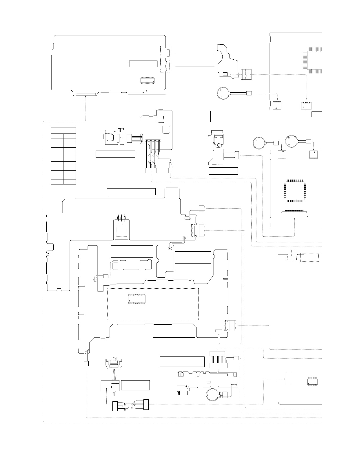
MD-X60
0
4
SO301B
COLOR TABLE
BR
BROWN
RD(R)
OR
ORANGE
YL
YELLOW
GR
GREEN
BL
BLUE
VL
VIOLET
GY
GRAY
WH(W)
WHITE
BK
BLACK
PK
RED
PINK
CNP303
113
JK151
MD IN/AUX1
MD JACK PWB-J
FE302
IC302
TUNER PWB-B3
1
6
CNP151
CNS151
6
CNS630
11
1
WH
WH
CNS401
CNS601
6
RD
1
OPERATION PWB-B2
JOG701
CD EJECT
SWITCH PWB-B7
12
CNP703
MD MECHANISM
SWITCH PWB-E
CN1901
M903
LOADING
MOTOR
MD INPUT
VR630
LEVEL PWB-B4
1
WH
GY
GY
GY
PK
WH
CNS550
1
CNS706-B
1138
2
CNS706-A
RD
WH
4
1
CFW702
1
CFW705
2
1
9
DECK SWITCH
PWB-B6
MD PICKUP
4
1
1
9
RD
BK
FLEXIBLE PWB
FLEXIBLE PWB
CW1901
1
1
5
5
1
2
MD SPINDLE
MOTOR
M901
RD
BK
2
1
MD SLED
MOTOR
1
2
2
CN1603
28
CN1604
M902
1
IC1201
CN1101
SW101
IC1
5
1
CN1601
MD
RD
1
2
BK
12
CN16
1
JK401
CNS704
3
CNS703
GY
31
1
2
RD
WH
RD
1
RECORF/PLAY BACK/
ERACE HEAD(217-1)
61
2
1
CNS101A
FLEXIBLE PWB
TAPE HEAD
PWB-G
WH
BK
1
6
GY
WH
IC712
WH
WH
7
1
CNS101B
FL711
DISPLAY PWB-B1
TAPE MECHANISM
PWB-F
SW4SW5
SOLENOID
SOL 1
SW3
TAPE MOTOR
(217-2)
1
1
CFW701
CNP702
1
4
11 1
GY
1
1
SW2
MM1
8
8
CNS103CNS102
2
1
RD
13
FWM2
13
SW1
14
B
1
7
CNP101
IC101
Figure 30 WIRING BLOCK DIAGRAM (1/2)
– 30 –
Page 31

MD-X60
IC1401
5
1
CN1601
MD MAIN PWB-D (BOTTOM)
D
1
2
K
12
CN1602
1
MD MAIN PWB-D(TOP)
JK401
1
CNP401
8
4
1
CN1904
24
1
CN1252
2
1
CN1902
4
1
CNS1904
MD FLAT CABLE
1241
SW951
BK
WH
(42)
2
1
CNS1252
SW901
24
BK
BK
POWER AMP. PWB-C1
GY
BK
YL
2
1
CNS960
CNP261
12
CNP820
MAGNET
HEAD
(40)
CNP550
JK620
BR
YL
6
BL
1
6
GY
CNS3A
FUSE PWB-C3
1
CNS802B
12
BR
1
CNS801A
1
BR
T801
POWER TRANSFOMER
M702
SLED MOTOR
+
-
1
1
CNP3A
6
6
1
CNS801B
13
CNS802A
(261)
AC CODE(257)
+
BR
YL
CNP801
7
1
YL
12
13
YL
K801
(261)
AC120V 60Hz
-
M701
SPINDLE MOTOR
3
1
CNS850
YL
RD
K802
TO MD UNIT
CNS851
7
CNP850
1
IC201
1
CNP201
6
CNP810
1114 15
21
CNS261
BR
RD
M271
FAN MOTOR
1
6
CNS201
HEAD PHONE
PWB-B5
MAIN PWB-A
UNA901
2
1
CNP960
DIGI IN
2
1
CNP3
CNP2
6
1
1
8
CNS970A
WH
BK
13
YL
7
1
RD
SO201
CNS620
1
WH
RD
POWER PWB-C2
CNS3B
CD MOTOR PWB-H
IC101
1
CNP1
7
1
CNP11
4
5
1
CNP990
6
1
CNP980
CNS1B
CNS2B
CNS2
BIM3
BK
1
8
GY
RD
1
7
WH
1
8
CNS2A
1
7
81
BIM1
YL
4
1
MOB2 MOB1
OR
BR
YL
RD
BR
PICKUP UNIT
71
CNS1A
TRAY SWITCH PWB-I
5
YL
5
BIM2
1
BL
1
BL
6
1
BR
SWB104CAM4
SWB103CAM3
SWB102CAM2
SWB101CAM1
CNP950
2
CNS970
GY
BK
WH
1
1
CNP910
15
1
CNP103
12
CNP920
14
11
CNP102
1
9
CNP930
1
IC901
8
1
CNP940
1
CNP925
13
1
2
23
24
Figure 31 WIRING BLOCK DIAGRAM (2/2)
– 31 –
Page 32

MD-X60
D6.5/4.75 ~ 5.25V
MECHANISM
6.5/4.75~5.25V
D3.2V
AVCC
DVDD
DVDD
D3.2V
DIGITAL
3.2V
D3.2V
D4.3V
A3.2V
D4.3V
D3.2V
D4.3V
D3.2V
VOLTAGE
REGULATOR
POWER
EEPROM
MOTOR
DRIVER
IC1601
VOLTAGE
REGULATOR
POWER
AUDIO INPUT
AUDIO OUTPUT
MD
MICROCOMPUTER
MD
CONTROL
MICROCOMPUTER
IC1401
DIGIN(EIAJ)
PDOWN
DIGOUT(EIAJ)
GND
GND
1
1
224
3
PLL
D/A
CONVERTER
A/D
CONVERTER
R.IN
R.OUT
AA.GND
AD.GND
AA.GND
L.IN
L.OUT
LOAD IN
RESET
MD-ST
DSCK
SERCH
1
2
242322
21
20
1918171615
14
45678
9
13
101112
3
D.GND
D.GND
D.GND
D.GND
DSTB
MDDATA
KDATA
4M
DRAM
ENDEC/ATRAC
IC1201
OSCILLATOR
XL1201
(33.8688MHz)
SW1956
SW1955
SW1954
SW1953
SW1952
Q1251~Q1254
MD
RECORDING
HEAD
M901
SPINDLE MOTOR
M902
SLED MOTOR
M903
LOADING
REC
PLAY
LEAD IN
A–BSIGNALE–FSIGNAL
RF1 ~ RF4SIGNAL
HEAD
DRIVE SIGNAL
IC1251
RF SERVO/
SIGNAL
CONTROL
IC1101
LOADING MOTOR
HEAD UP/DOWN
M
M
DIRECT
WRITE PRO
M
LASER DIODE
MONITOR DIODE
RF4
RF3
RF2
RF1
LIGHT
RECEIVING
SECTION
ERROR
SIGNAL
LIGHT
RECEIVING
SECTION
RF
FAB
E
FOCUS
TRACKING
PICKUP UNIT
Figure 32 BLOCK DIAGRAM (1/4)
– 32 –
Page 33

OPTICAL PICKUP
SW702A
31
FOCUS/TRACKING/
8
9
10
11
12
13
242530
7
IC5
M56748FP
SPIN/SLED
DRIVER
343536
27 262829
20
+B1
MD-X60
M702
SLED
M
MOTOR
FOCUS COIL
TRACKING COIL
M701
SPINDLE
M
MOTOR
6
1
5
14
22
32
15
16
27
23
29
30
31
54
50
51
52
53
4
1
3
2
F
TO
FD
SPO
SP
SLD
SL–
SL+
DRF
CLK
CL
DAT
CE
E
FIN2
FIN1
IC1
LA9241M
SERVO CONTROL
SL
CV+
SLC
RFSM
~
41
44
62
LD0
64
VCC1
JP–
324043
OPTICAL PICKUP UNIT
LASER DRIVER
Q1
+5V
OPTICAL
PICKUP
VOLTAGE
REGULATOR
+7.3V (B2)
IC1,IC2
+5V
Q81
+5V
PU-IN SW
CAM SWITCH
TRAY SWITCH
SWB101
SWB102
SWB103
SWB104
SWB105
SWB106
SWB107
SWB108
SL+. SL–. DRF
CD–D–OUT
JP–
JP+
CL, DAT, SELIAL CONTROL/CE
63
~
68
72
1
MAIN CAM MOTOR
9
1
TRAY MOTOR
9
TGL
SERVO SIGNAL
RES. CQCK. COIN
SQOUT. RWC. WRQ.4M
56
3
7
IC92
TA7291S
DRIVER
IC91
TA7291S
DRIVER
3
7
~
192023242829
V/P
HLF
TES
TOFF
IC2
LC78625E
6
5
6
5
111315
CLV+
EFMIN
+B1
10
EFMO
XIN
XOUT
VVDD
VDD
LVDD
RVDD
XVDD
767551504039842
M
M
77
78
6
27
47
54
79
MAIN CAM
XL1
16.934MHz
MOB1
MOTOR
MOB2
TRY
MOTOR
+5V
MAIN SECTION
(TO µ-CON)
Figure 33 BLOCK DIAGRAM (2/4)
– 33 –
Page 34

ANTENNA
AM LOOP
Figure 34 BLOCK DIAGRAM (3/4)
– 34 –
AM
GND
75ohms
FM
GND
TERMINAL
ANTENNA
SO301
MD-X60
2
OUT
IC303
23
IN
+B4
AM IF
T351
CF352
4
IN
FM IF DET./FM MPX./AM IF,
22
AFC
LA1832S
21
7
STEREO
AM RF IN
IF
OUT
13
10
6
SD
FM IF
AMP
FM IF
8
FM FRONT END
1
Q301
CF302
FE301
2
6
7
3
OSC.
FM
5
4
VT
FM MUTE
LEVEL
VR351
FMOSC
FM IF IN
1
AM OSC
24
OUT
AM RF
FM MONO/STMONO/ST
4.5MHz
X352
T302
COIL
1
OSC.
AM
AFC
8
2
AM RF
7
AM OSC.
14
AM
ANT.
COIL
3
12
13
9
FM +B
+B4
Q360
FM
20
1
OSC.
7
AM IN
XT21
FM IN
22
15
16
10
11
IC302
TC72131
PLL CONTROLLER
4
3
5
CL
CE
DI
IF IN
12
21
6
DO
5
GND
11
PHASE
MPX
REGURATOR
+B4
+5V
17
CF351
+B4
9
8
VCC
12
CUT
VOLTAGE
7
X351
17
MPX
VCO
OUT
14
15
R
L
MUTING
Q354
TUNER MUTE
18
FM/AM
Q353
IN
16
MPX
SD
+B4
5V
Q371
TO µ-COM
Page 35

IC201
POWER AMP.
STK40705
IC710
INVERTER
TC7WU04F
IC912
NAND GATE
74HC00F
IC902
RESET
PST9140
IC903
EEP ROM
S29194A
IC951.IC952
BAND PASS FILTER
BA3835F
IC711
M35500AF
FL DRIVER
IC712
IX0069AW
FL DRIVER
FL711
DISPLAY
Q850
Q851
Q820
Q821
Q830
Q831
Q880
Q881
Q101
Q102
Q840
Q841
Q860
Q861
Q801
Q811
–B1
(–11V)
+B3
(+12V)
+B5
(+5V)
REGURATOR
VOLTAGE
REGURATOR
VOLTAGE
REGURATOR
+B4
(+11V)
+B7
(+5.6V)
+B1
(+9V)
+B2
(+7.3)
+B6
(5.6/6.8V)
10
14
1
2
8
3
15
7
6
+B
–B
R-OUT
L-OUT
RL201
RELAY
Q271
Q272
M
FAN MOTOR
ON–OFF
SW
RIGHT
LEFT
IC401
AUX1/AUX2
INPUT SELECTOR
BU4052BCF
IC101
EQUALIZER
AMP.
M51167BFP1
IC103
DOLBY NR
HA12134AF
IC102
HEAD SELECTOR
BA3126N
IC501
LC75396E
AUDIO
PROSSESOR
IC552
BUFFER AMP.
NJM4565M
–B1
+B4
385
4
7
1
OUT
AUX2
IN
JK401
ANALOG IN/OUT
526051615458535955
57
63 49 48 64
19
21
18
16
1
31
17
23 25
56 26
29
27
30
32
47
293
10
1
11
12 14
57
VR630
INPUT
LEVEL
128 126
1
1
3
7
2
3
67 6596 70
113
97
122 114
64 62 59 33
6260 6444 58 5935 43
60 19
18 9 28
61128
33
4
25
12
24
13
13 2215 23 31
1
14
1
X701
234
876
5
44 3
7
9
12
Q701
Q703
Q704
Q715
Q716
Q724
27
43
18
26
15
5
12
11
131210
14
6
SW731 735
SW741 748
SW751 757
SW701 707
SW711 715
SW721 725
SW736.737
SW716 718
46
385354 13
17
10
29
568
697036
47
49
6
3
28
39 41 42 43
44
55
56
656362
678820
22
84 86 87 40
100
16 18
9
8
14
23 27
JOG701
VOLUME
Q501
Q502
+B4
+B5
REMOTE
SENSOR
12
3
+B5
+B5
+B5
SW951
RESET
~
4749
~
1210
~
~
L
R
L
L
R
L
R
30
7
L
R
29
8
14316
1
L
R
L
RLR
22
23
R
L
L
R
R
L
R
L
R
LRLRLRL
R
~
71 80
~
93
21
99
~
57 92 91 85
NAME IN
APSS IN
REC MUTE
REC MUTE
CONTROL
CrO
2
SWITCHING
DORBY RWC/PB
DORBY ON/OFF
PB MUTE
PLAY
MUTE
CONTROL
SWITCHING
BIAS COTROL
BIAS
OSC
SWITCHING
SWITCHING
REC CONT
REC BIAS
MOTOR
SOL
RUN PLSE
BUFFER
SPEANA
RX701
18 17
1
2
4
5
13
18 17
1
2
4
5
11
13
A/D SW
RA121 RA130
~
~
18 17
1
2
4
5
13
~
~
~
21
9
5
12
2
8
3
19 36
11 26
2
37 19
6
4
5
8
Q103
Q104
Q113
Q114
+B4
B
A
SW5
SW1
SW3
SW4
R–REC
F–REC
PACK
CrO
2
SOL1
SOLENOID
SW2
PLAY
MM1
SW101
BEAT CANCEL
TAPE MOTOR
RLY-OUT
F8025AF803
5A
F804
2.0A
F805
2.0A
+B5 +B5
IC911
BU2092F
INPUT
SELECTOR
IC912
BU2092F
INPUT
SELECTOR
IC771
BU2092F
INPUT
SELECTOR
JK151
MD IN/AUX1
AUX1/MD-MD
EDIT
Q901
LED771
LED782
+B3
SW1
SW9
~
+B5
SW1
SW9
~
SW1
SW9
~
X901
6MHz
X902
IC901
SYSTEM CONTROL MICON.
IX2757AF
FROM CD SECTION
FROM MD SECTION
TO TUNER SECTION
FROM TUNER SECTION
~
4
8
~
GE
~
~~
+
–
–
+
NAME-IN
D-GND
L-IN
R-IN
A-GND
L
L
R
R
–B1
+B4
~~
~~~~
~~
~
~
~
~~
~
~
~
~
D812~D815
–B2
D802~D805
D801
AC CODE
AC120V 60Hz
T801
POWER TRANSFORMER
M971
FAN MOTOR
SO201
SPEAKER TERMINAL
RATED SPEAKER
IMPEDANCE:6 OHMS
JK901
HEAD PHONES
UNA901
AUX OPT.
DIGITAL IN
~~~
~~
~~
+B5
SWITCHING
SWITCHING
SWITCHING
SWITCHING
+B5
+B4
+B4
+B
+B
+B3
+B3
+B3
–B2
–B2
~
–B2
+B5
+B5
~~~~~~~
~
~
RECORD/
PLAYBACK HEAD
VR101
VR102
ERASE HEAD
EH
Q106 Q109
VR107
TAPE SPEED
VR105,VR106
REC SENS.
Q111
Q112
Q108Q110
PHM1
M
Q117
Q115
Q118
Q119
Q116
SWITCHING
TO MD SECTION
CAM SWITCI
FROM CD SECTION
TO MD SECTION
MOTOR DRIVER
SOLENOID DRIVER
MD-X60
Figure 35 BLOCK DIAGRAM (4/4)
– 35 –
Page 36

MD-X60
R
0
B
560
V
A
B
C
D
E
F
G
TAPE HEAD
PWB-F
RECORD/
PLAYBACK HEAD
L-CH
R-CH
EH
ERASE HEAD
R111
C107
0.22/50
6.8K
4.4V
4.4V
EQ AMP NF 2
ALC VALIABLE
RESISTANCE 2
OUT 1
ALC
VALLABLE
REC
4.4V
4.3V
C110
C108
0.22/50
R121
15K
R122
15K
47K
C117
1/50
R109
C109
270P
NC
REC AMP IN
AMP IN 1NCALC
270P
R110
5.6K
TAPE SIGNAL
RECORD SIGNAL
C128
220/10
C103
220/10
R103
39
R101
1K
8.5V
8.0V
C101
560P
C130
33/16
7
1
1
2
2
3
3
4
4
5
5
6
6
CNS101A
7
6
6
5
5
4
4
3
3
2
2
1
1
CNP101
CNS101B
C148
R133
10/16
1K
0.1V
C102
0V
0V
0V
R158
1
2
3
4
2.2K
5
560P
REC SW REC SW
P/B SW P/B SW
CONT
0V
HEAD SELECTOR
0V
HEAD IN 2-A
RIOOPLE FILTER
IC101
M51167BFP1
HEAD IN 1-A
GND
EQUALIZER AMP.
123456789
0V
0V
R102
1K
9
0V
0V
8
7
0V
10.6V
6
IC102
BA3126N
VCC
DABBIMG
0V
C112
270P
C105
0.033
C111
270P
0V
1.2V
HEAD IN 2-B
EQ AMP NF 2
SW CONTROL
HEAD IM 1-B
EQ AMP NF 1EQEQUALIZER 1
0V
1.2V
C106
0.033
R104
39
C104
220/10
+B
R107
3.9K
R105
4.1V
4.1V
EQ
EQUALIZER 2
EQ AMP
4.1V
4.1V
R106
6.8K
R108
3.9K
TP101
R136
10
R129
10K
R135
R-CH REC
FREQUENCY
VR102
22K(B)
C146
330P
C142
560P
10
VR101
22K(B)
L-CH REC
FREQUENCY
C145
330P
C140
0.0082
C139
0.039
Q111
DTC143 TK
2
0V
2
0V 3.8V
C138
0.047
(ML)
1
1
R156
22K
R154
L101
330µH
3
3.8V
0V
0V
3
Q112
DTC143 TK
Q110
2SC3242 G
47K
0V
0V
C143
0.022
0V
R155
R134
1K
4.7
POSISTOR
RP101
C141
100/16
A
B
SW101
BEET CANCEL
R117
1.8K
C121
560P
C119
0.0033
5.6K
4.3V
4.4V
4.3V
2627 25 24 23 22 21 20 193536 34 33 32 31 30 29 28
ALC
NF 2
TAPE
REC AMP
DETECTOR 2
DETECTOR
REC
AMP NF 1
REC AMP
1110 12 13 14 15 16 17 18
4.3V
4.4V
4.4V
C114
1/50
R116
1M
C122
560P
C118
R112
R130
8.2K
Q105
2SB561 C
0V0V
0V
R144
15K
R113
2.2M
C113
1/50
C115
0.001
0.5V0V0V
0.5V
TAPE
TAPE
EQUALIZER
EQUALIZER A
EQUALIZER B
OUT 1
R/P SW
CONTROL
ALC DRIVE
0V
0V
R128
1M
C120
0.0033
R114
2.2M
C124
180P
(CH)
1/50
47K
R118
R131
100
R145
150
R148
33 (1/2W)
R143
56K
C123
180P(CH)
R115
1M
A/B SW
CONTROL
MUSIC SENSER
NOISE FILTER
0.3V
1.8K
R146
150
R147
33 (1/2W)
R157
5.6K
R119
R123
220
C125
10/16
0.4V
MUSIC
MUSIC
SENSOR CR
SENSOR GND
MUSIC SENSER
GAIN CONTROL
MUSIC SENSER
OUT
5.1V
3.4V
C147
10/16
REC IN
EQ OUT
C116
0.001
C150
100P(CH)
0V
R120
120K
Q106
KRA107 S
120K
C149
0V
0V
R124
100K
C129
R125
1/50
1.5K
R127
2.2K
R126
C132
0.1/50
C131
0.1/50
C126
10/16
32
0.5V
1
0V
11V
3
11V
1
2
0V
Q107
DTC144 EK
2
0V
1
0V
100P
(CH)
32
0.5V
1
EQ OUT
REC IN
REC OUT
R132
4.7K
470K
REC OUT
Q102
DTC144 EK
+B
3
0.5V
Q101
DTC144 EK
Cro2
C151
0V
0.47
Q1
2S
5
11
R152
2
H
• NOTES ON SCHEMATIC DIAGRAM can be found on page 62.
1
23456
Figure 36 SCHEMATIC DIAGRAM (1/15)
– 36 –
Page 37

MD-X60
C151
0.47
+B
R199
560
Q108
2SB561 C
11V
0V
11V
C136
R152
560
11V
Q109
2SC2412 KR
M
MM1
TAPE MOTOR
SW2 PHM1
PLAY
SOL1
SOLENOID
SW4
CrO
2
SW3
PACK
SW1
F–REC
SW5
R–REC
C169
4.7/50
C155
220P
PB IN
220P
C159
1/50
C170
4.7/50
TAPE
SPEED
VR107
2.2K(B)
R196
390
R197
2.7K
PLAY SW
+5V SENSOR
SENSOR OUT
R_REC
REC IN
C157
330P
R163
-COM
+MTR
+SOL
CrO2
PACK
F_REC
VR105
47K(B)
270
NC
10/16
0V
R141
100K
R153
56K
0.45V
R150
4
B
A
+
–
1
100K
R137
5.6K
R161
27K
VR103
22K(B)
L-CH PLAY
VR104
22K(B)
R-CH PLAY
R162
27K
R149
C137
47/16
Q103
2SC2412 KR
0.1V
R159
2.2K
C153
1/50
SENS.
C175
390P
SENS.
R160
2.2K
R138
5.6K
0.7V
Q104
2SC2412 KR
5.6K
MOTOR SPEED B
MOTOR SPEED A
470
0V
0V
C154
1/50
C156
L103
6.8mH
0V
0V
TAPE MECHANISM PWB-F
R171
6.8K
4.8V
16 15 14 13
BIAS
1234
9.8V
4.8V
REC IN
C158
330P
L104
6.8mH
C160
1/50
13
13
12
12
11
11
10
9
8
7
6
5
4
3
2
1
FWM2
L-CH REC.
SENS.
C167
10/16
R173
18K
4.8V
0V
C171
220/10
C176
390P
C168
10/16
12V
L105
4.7µH
0.8V
C178
47/16
CNS103
10
9
8
7
6
5
4
3
2
1
PB IN
BIAS
SW
SW
4.8V
C172
1/50
C173
10/16
Q117
2SB561 C
CNP103
1
2
1
2
3
4
5
6
7
8
9
10
CNS102
R165
22K
REC/PB
5.1V
0.9V
PB OUT
121110
BUF
AMP
567
0.7V
4.6V
4.8V
NR ON/OFF
R172
6.8K
10K
R175
R195
820
R194
100K
1
2
1
2
3
4
5
6
7
8
9
111011
CNP102
R167
1K
C165
0.22/50
4.8V
SIDE
CHAIN
SIDE
CHAIN
PB OUT
DET
1.3V
C161
1.3V
DET
C166
R191
470
10/16
REC OUT
4.8V
9
8
REC OUT
4.8V
C162
22/50
R168
VR106
47K(B)
R-CH REC.
SENS.
+B
C163
10/16
IC103
DOLBY NR
HA12134AF
C164
10/16
10/16
1K
R164
R166
22K
12V
D103
1SS133
0V
Q119
2SB561 C
1K
3
2
1
TP102
R187
12V
3
2
1
R184
R179
100K
100K
R169
12K
R170
12K
R180
100K
47K
C177
10/16
Q116
KRC107 S
R186
1K
Q113
2SJ103 GR
0V
C
11V
11V
0V
C
Q114
2SJ103 GR
Q115
KRC107 S
0V
3
0V
1
12V
2
Q118
KRC107 S
D
0V
R177
G
C174
0.22/50
G
AUDIO+12V
5.1V
2
1
12V
5.6K
R181
330K
D102
1SS133
D
0V
R178
5.6K
R183
150K
R182
R193
3.9K
150K
R192
3.9K
R185
4.7K
DOLBY-REC/PB
DOLBY-ON/OFF
0V
3
0V
32
0V
0V
1
MAIN PWB-A(1/4)
R-CH
REC-R-CH
BIAS_GND
MECHA GND
M_12V
REC-BIAS
REC-CONT
R/P-CR02
REC-MUTE
PB-MUTE
A/D-5V
APSS-IN
RUN_PLSE
SIDE_B
CR02_SW
CASSTE_SW
SIDE_A
MAIN_SW
MOTOR
L-CH
REC-L-CH
TP16
TP20
TP11
TP15
TP17
TP10
TP12
TP23
TP21
TP14
TP22
TP13
SOL
TP18
TP19
TP1
101
102
103
TP2
P40 5-A
104
TP3
105
TP4
MAIN PWB (3/4) AUDIO PROCESSOR SECTION
TP5
A
B
C
D
TP6
E
F
G
H
I
TP8
J
TP9
K
TP7
L
P39 7-H
M
N
O
P
Q
TO MAIN PWB (2/4) SYSTEM CONTROL SECTION
R
S
T
U
V
7
8 9 10 11 12
Figure 37 SCHEMATIC DIAGRAM (2/15)
– 37 –
Page 38

MD-X60
T
A
B
7
E
D
P
0V
INPUT/OUTPUT
C958
390P
150P (CH)
0V
1
VSS
5.1V
2
DATA
5.1V
3
CLK
5.1V
4
LCK
11V
5
SW1
6
SW2
7
SW3
8
SW4
9
SW5
C911
0.1
5.1V
IC903
S29194A
EEP ROM
C917 100P
C916 100P
C918 100P
POWER
EXP_LCK3
EXP_LCK2
EXP_LCK1
R919 1K
R918 1K
R917 1K
R916 1K
1819
LCK2
LCK3
POWER
0V
5V
4.5V
IC901
IX2757AF
1.3V
4.7V
AVREF1
FLD_CS1
FLD_CS2
5.1V
R963 1 K
R962 1 K
R965 1 K
FLD_DO
FLD_CS1
FLD_CS2
IC912
BU2092F
EXPANDER
SW12
SW11
SW10
0V
0V
0V
0V
3V
0V
5V
11V
+B
0V0V1V
8
DO
GND
PROT
NC
VCC
CS
1234
5.1V0V5.1V
C915 100P
C914 100P
EXP_CLK
EXP_DATA
R914 1K
R915 1K
R913 1K
R912 1K
151617
CLK
LCK1
DATA
EEP-CS
5V5V5V
5.1V
5.1V
4.7V
4.8V
4.9V
MD-DATA
FLD_A/D IN
FLD_DATA
FLD_CLK
R968 1 K
R967 1 K
R966 1 K
R969 1 K
FLD_DI
FLD_CK
MDDATA
VDD
OE
SW9
SW8
SW7
SW5
567
DI
SK
EEP-SK
0V
0.3V
K-DATA
KDATA
11 10121314
5.1V
18
0V
17
16
15
RA163
14
1K
13
RA161
12
1K
11
10
RA160
R911 1K
R910 1K
EEP-DI
EEP-DO
0V
0V
CD-MUTE
CD_HI-SPEED
3.9V
4.9V
DSLK
RES
R970 1 K
R971 1 K
DSCK
RES_CD
0
SEARCH
R908 1K
89
VDD
0V
5.1V
VSS
MAIN SW
0V
0V
SQOUT
RWC
R973 1 K
R972 1 K
SQOUT
RWC
DIG_B
DB_ON/OFF
PB_MUTE
LOAD_SW
MD_ST
R907 1K
R906 1K
S-ID
SYN
LOAD
0V
0.7V
TAPE
100
99
82
81
4.9V
4.9V
CQCK
COIN
R974 1 K
R975 1 K
COIN
CQCK
RA181
10K
RESET
R905 1K
567
RESET
0V
WRQ
7
767574737270 7169686766656463626051 615958575655545352
R976 1 K
WRQ
V_LOAD
R903 1K
4
VLOAD
C
1V
DRF
R977 1 K
DRF
IC911
BU2092F
A
EXP_DATA
EXP_CLK
RA102 100K
EXP_LCK1
RA103 100K
RA104 100K
RA122
2.2K
RA121
R1078
18K
Q946
2SC2412 KR
CY998
120P
0
R1029 5.6K
R1030 5.6K
R1031 5.6K
R1032 5.6K
R1033 5.6K
R1034 5.6K
R1035 5.6K
R1036 5.6K
R1044 22K
R1045 22K
R1046 12K
R1047
470K
0V
B
A/D_SW
20
AUX_1/2
21
NAME_IN
22
A_GND
P41 11-D
23
MAIN PWB (3/4)
AUDIO PROCESSOR SECTION
TP951
1
TP952
C
D
E
2
3
P45 9-G
4
CD SECTION
5
TO MAIN PWB (4/4)
CNP980
1
2
3
4
BIM3
5
6
1
P45 12-G
CD SECTION
2
3
TO MAIN PWB (4/4)
CNS2
4
5
CNP990
6
7
8
9
10
11
12
13
P45 7-G
CD SECTION
14
15
TO MAIN PWB (4/4)
16
17
18
SW951
RESET
TP953
TP954
TP955
D_GND
CAM_SW1
CAM_SW2
D_GND
CAM_SW3
CAM_SW4
D_GND
TRY_SW1
TRY_SW2
TRY_SW3
TRY_SW4
TP916
TP915
TP914
TP913
TP912
TP911
TP910
TP909
TP908
TP907
TP903
TP902
TP901
C929
100P
PU_IN
SL+
SL–
DRF
WRQ
CQCK
COIN
SQOUT
RWC
RES_CD
CD_9V
CD_7V
CD_GND
MO_H/L
C-MO_FOR
C-MO_REV
T-MO_FOR
T-MO_REV
C930
100P
C931
C932
100P
100P
C936
C935
100P
100P
C934
100P
C933
100P
C902
150P (CH)
RA123
+B
0V
DUBB MODE
0V
0V
2.7K
5.1V
C903
150P (CH)
STOP
SKIP+1
SKIP+10
PLAY N
RA124
C945
C904
5.1V
5.1V
5.1V
3.3K
0.1
INPUT/OUTPUT
EXPANDER
390P
0V
1
VSS
2
DATA
3
CLK
4
LCK1
5
SW1
0V
6
SW2
7
SW3
8
0V
SW4
9
SW5
0V
RA125
3.9K
RA126
4.7K
RA127
+B
CAM_SW1
CAM_SW2
CAM_SW3
CAM_SW4
TRY_SW1
TRY_SW2
TRY_SW3
TRY_SW4
C943
0.1
RES
C942
18P (CH)
RX_IN
PROTECT
VDD
OE
SW12
SW11
SW10
SW9
SW8
SW7
SW5
6.8K
X901
6MHz
22P
C941
SPEANA_A
SPEANA_B
SPEANA_C
RA128
(CH)
5.1V
18
0V
17
0V
16
AUX_1/2
15
0V
14
NAME SEL
13
DATA SEL
12
NEXT
11
PLAY 1T
10
0V
10K
32.768kHz
C908
0.1
0V
RA129
15K
R931 1K
R932 1K
R933 1K
R934 1K
R935 1K
R936 1K
R941 330K
X902
5.1V
5.1V
5.1V
3.0V
3.0V
2.0V
3.8V
C951
DSTB
0.1
C952
0.1
8V
0V
0V
RA130
R938 0
R943 1K
R944 1K
R945 1K
R946 1K
R947 1K
R948 1K
R949 1K
R950 1K
RA132
100K
RA131
39K
22K
R930
1K
0.2V
0.2V
0.2V
0.2V
5.1V
5.1V
5.1V
2.5V
SPEANA_L
SPEANA_R
+B
RA115
1K
AUX_1/2
R1028
R929
1K
0.2V
31
32
33
34
TRY SW2
35
TRY SW3
36
TRY SW4
37
VDD
38
MAIN CLK OUT
39
MAIN CLK IN
40
VSS
41
SUB CLK OUT
42
SUB CLK IN
43
RESET
RX IN
44
PROTECT
45
NAME IN
46
SPE_ANA-A
47
48
49
50
5.1V
C957
C956
150P (CH)
EXP_DATA
RA152 1K
EXP_CLK
RA153 1K
EXP_LCK2
RA154 1K
REC_BIAS
REC_CONT
CRO2
REC_MUTE
DB_PB/REC
RA178 3.3K
RA179 22K
RA177 2.2K
RA155 1K
RA156 100
RA157 220
RA158 100
RA159 1K
RA176 3.3K
27K
R1022 47K
R1026 27K
R1025 27K
R1024 27K
R1027 27K
FLD_RES
T-MO_REV
T-MO_FOR
C-MO_FOR
C-MO_REV
FAN
VPP
RELAY
MO_H/L
R923 1K
R924 1K
R925 1K
R926 1K
R927 1K
R928 1K
0.2V
0.8V
5.0V
0.8V
2829
CAM SW1
CAM SW2
FLD RESET
TRAY MOTOR REV
TRAY MOTOR FOR
SYSTEM CONTROL MICROCOMPUTER
3.0V
3.0V
5.1V
5.1V
JOG-A
AVDD
AVREF0
SPE_ANA-L
SPE_ANA-R
0V
0V
0V
R953 1 K
R954 1 K
R955 1 K
JOG_A
0.8V
0.1V
0.8V
252627
MOTOR H/L
CAM MOTOR REV
CAM MOTOR FOR
31
CAM SW3
32
CAM SW4
33
TRY SW1
48
SPE_ANA-B
49
SPE_ANA-C
50
DSTB
0V
0V
4.6V
JOG-B
INITIAL AREA 1
TEMP
R956 1 K
R957 1 K
R958 1 K
JOG_B
TEMP
R921 1K
0V
2130 20222324
TEST/VPP
FAN MOTOR
0V0V0V
5.1V
0.3V
RDS
VSM
SPAN SEL.
R960 1 K
R959 1 K
VSM
R920 1K
RLY_OUT
0V
AVSS
IC902
PST9140
F
G
RESET
1
5.1V5.1V
2
3
0V
2.6V
C961 0.1
1
1.6V
2
2.6V
C962 0.1
3
RA263 100K
4
5
6
2.6V
C967 0.1
C968 0.1
C969 0.1
7
2.6V
8
5.1V
9
BAND PASS FILTER
BIASC
VREFC
RREF
N.C
DIFOUT
N.C
CIN
AIN
Vcc
IC951
BA3835F
R1043
47K
+B
C944
0.1
0V
GND
18
SPEANA_R
0V
5.1V
SPEANA_C
SPEANA_B
SPEANA_A
0V
+B
17
AOUT
16
TEST
15
N.C
14
SEL
13
N.C
12
0V
C
4.9V
11
B
0V
10
A
H
• NOTES ON SCHEMATIC DIAGRAM can be found on page 62.
1
23456
Figure 38 SCHEMATIC DIAGRAM (3/15)
C971
0.1
C972
0.1
RA272
100K
C979
0.1
– 38 –
C977
0.1
C978
IC952
BA3835F
BAND PASS FILTER
2.6V
1.6V
2.6V
2.6V
0.1
5.1V
1
2
3
4
5
6
7
8
9
BIASC
VREFC
RREF
N.C
DIFOUT
N.C
CIN
AIN
Vcc
GND
AOUT
0V
TEST
0V
2.6V
4.9V
0V
C964
R1062 10K
R1063 10K
R900
56K
0.1
C999
68P
MOTOR
TP961
SOL
TP962
MAIN_SW
SIDE-A_SW
TP969
TP968
SIDE-B_SW
CASSETTE_SW
CRO2_SW
TP967
TP966
TP965
+
APSS
D_+B
RUN_PULSE
TP964
TP963
MNOPQRSTUV
TO M
TAPE
TP999
+B
0V
18
SPEANA_L
17
0V
16
15
N.C
14
SEL
5.1V
13
N.C
12
C
11
B
10
A
SPEANA_C
SPEANA_B
SPEANA_A
C950
220/10
R1055 10K
R1056 10K
RA252
4.7K
RA251
4.7K
R1058 10K
R1059 10K
R1057 10K
RA254
33K
RA253
33K
Page 39

MD DATA
EEP
CS
CS
DO
3
8
0
0
0
4.8V
5
1V
MD-X60
MAIN PWB-A(2/4)
12
92F
UTPUT
DER
5.1V
18
VDD
0V
17
OE
16
SW12
15
SW11
RA163
14
SW10
1K
13
SW9
V
RA161
12
V
SW8
1K
11
SW7
V
10
SW5
1V
RA160
0
0V0V
5
DI
SK
4
R912 1K
R911 1K
R910 1K
R908 1K
11 1012
-
VDD
EEP-DI
EEP-SK
EEP-DO
5.1V
0V
0V
0V
.
MAIN SW
OCOMPUTER
CD-MUTE
CD_HI-SPEED
0.3V
4.9V
0V
3.9V
DSLK
K-DATA
RES
RWC
R969 1 K
R970 1 K
R971 1 K
R972 1 K
KDATA
DSCK
RWC
RES_CD
DB_ON/OFF
PB_MUTE
LOAD_SW
SEARCH
R907 1K
89
SYN
LOAD
0V
0.7V
100
VSS
4.9V0V0V
COIN
SQOUT
R973 1 K
R974 1 K
SQOUT
COIN
DIG_B
RA181
RESET
MD_ST
R906 1K
R905 1K
567
S-ID
0V
TAPE
99
82
81
4.9V
CQCK
R975 1 K
R976 1 K
CQCK
WRQ
C970
0.1
10K
V_LOAD
R903 1K
0V
0V
RESET
VLOAD
0V
SIDE-A SW
CASSETTE SW
CrO2 SW
SIDE-B SW
RUN PULSE
TUNER MUTE
MIC MUTE
1V
0V
WRQ
DRF
SL–
R977 1 K
R978 1 K
DRF
SL–
MOTOR
SOL
R902 1K
R901 1K
1234
0V
MOTOR
APSS
MIC IN
S-MUTE
CCB-CL
CCB-DI
CCB-DO
CCB-CE
L-MUTE
0V
SL+
80797877767574737270 7169
R979 1 K
R980 1 K
PU_IN
SL+
SD
PU IN
SOL
CY952
120P
0V
100
99
98
97
96
95
94
93
92
91
90
89
88
87
86
85
84
83
82
81
5.1V
R1080
+B
0V
0V
0V
0V
0V
0.1V
5.1V
5.1V
5.1V
5.1V
5.1V
0V
5V
0V
0V
5.1V
0V
5V
5V
0V
22K
2.5V
2.5V
4.9V
2.5V
2.5V
4.9V
+B
R999 1K
R998 1K
R997 1K
R996 1K
R995 1K
R994 1K
R993 1K
R992 1K
R991 1K
R988 1K
R987 1K
R986 1K
R985 1K
R984 1K
R983 1K
R982 1K
R981 1K
IC921
74HC00F
NAND GATE
1
2
3
4
5
6
7
GND
0V
C909
0.1
MAIN_SW
SIDE-A_SW
CASSETTE_SW
CRO2_SW
SIDE-B_SW
RUN_PULSE
TUN_MUTE
S_MUTE
CCB_CL
CCB_DI
CCB_DO
CCB_CE
L_MUTE
APSS
Vcc
SD
4.9V
14
0V
13
0V
12
4.9V
11
0V
10
4.1V
9
4.9V
8
RA183
47K
R1099 22K
R1098 22K
R1097 22K
R1096 22K
R1095 22K
R1094 22K
R1093 22K
R1092 22K
R1085
22K
+B
RA241
10K
RA244
10K
RA247
Q951
Q952
10K
0V
0.7V
0V
2SC2412 KR
MDDATA
RA245
4.8V
10K
0V
2SC2412 KR
0V
DSTB
0.2V
3.7V
RA248
0V
10K
RA249
470K
Q953
2SC2412 KR
D_+B
D_GND
C1002
0.1
RA242
10K
RA243
470K
C1001
RA246
1000/6.3
470K
+B+B
1/50
C985
JPY945
C996
0.047
0.1
FM SIGNAL
CD SIGNAL
MD SIGNAL
RECORD SIGNAL
L912
2.2µH
RA232
3.9K
RA231
3.9K
+B
C993
0.1
RA234
100K
RA233
100K
L911
2.2µH
C992
L901
2.2µH
1/50
C991
0.1
1
2
3
UNA901
AUX OPT.
DIGI IN
Y
DIG_GND
GND
MD_RCH
MD_A_GND
MD_LCH
AD_GND
MD_A_GND
A_+B(MD)
D_+B(MD)
D_+B(MD)
DSTB
MDDATA
KDATA
SEARCH
DSCK
RESET
LOAD_SW
P_DOWN
D_+B5V
D_GND
FLD_CS1
FLD_DI
FLD_DO
FLD_CK
FLD_CS2
FLD_RES
JOG_B
JOG_A
D_GND
EXP_DATA
EXP_CLK
EXP_LCK3
RX_IN
J1038
1N4004S
D_+B(MD)
D_GND(MD)
A_+B(MD)
CD_GND
CD_GND
BIAS_GND
V_LOAD
A_GND
A_GND
A_+B(11V)
PROTECT
POWER
R_CH_OUT
A_GND
L_CH_OUT
RELAY
CNS970A
CNP960
R_IN
L_IN
CNP950
M_+B
D_+B
M_+B
M_GND
M_GND
CD_9V
CD_7V
D_+B
D_GND
D_GND
FAN
A_–B
1
2
X
TO MD MAIN PWB
1
CNS960
2
P57 12-B
MD FLAT CABLE
(42)
24
24
23
22
21
20
19
18
17
16
15
14
13
12
11
10
9
8
7
6
5
4
3
2
1
1
8
8
7
TO DISPLAY PWB
6
5
4
3
2
1
1
CNP940
9
9
8
7
TO OPERATION PWB
6
5
4
3
2
1
1
CNP930
14
13
12
11
10
TO POWER AMP. PWB
9
8
7
6
5
4
3
2
CNP920
1
15
14
13
12
11
10
TO POWER AMP. PWB
9
8
7
6
5
4
3
2
1
CNP910
CD SECTION
CNS970
TO MAIN PWB (4/4)
TO MD MAIN PWB
CN1902
P57 12-G
CFW701
P49 8-G
CFW705
P49 12-G
CNP820
P52 1-F
CNP810
P52 1-C
P45 12-C
C905
470/16
J1009
10K
CD_DIGI_IN
MD_D_OUT
D_GND(MD)
D_GND(MD)
D_GND(MD)
D_GND(MD)
MD_ST
SOL
TP962
MAIN_SW
SIDE-A_SW
TP969
TP968
SIDE-B_SW
CASSETTE_SW
CRO2_SW
TP967
TP966
TP965
7
APSS
D_+B
D_GND
DB_ON/OFF
RUN_PULSE
TP964
PB_MUTE
TP975
TP973
TP963
TO MEIN PWB (1/4)
TAPE DECK SECTION
P37 12-E
DB_PB/REC
REC_MUTE
TP972
TP970
CRO2
TP971
REC_CONT
M_+B
M_GND
REC_BIAS
BIAS_GND
A_–B
A_+B
TP976
TP974
TP977
A_+B
ABCDEGFHIJKLMNOPQRSTU
SD
VSM
TEMP
13 12 1110
A_+B
A_GND
CCB_DI
TUN_MUTE
TUN_RCH
TUN_LCH
9876
54321
CNP303
TO TUNER PWB
P60 6-B
CCB_DO
CCB_CE
CNP925
CCB_CL
CCB_CE
CCB_DI
A_GND
S_MUTE
D_GND
CCB_CL
TUN_RCH
TUN_LCH
MAIN PWB (3/4) AUDIO PROCESSOR SECTION
L_MUTE
MD_LCH
MD_RCH
P40 1-E, P40 4-A
A_GND
REC_RCH
REC_LCH
A_GND
68676665646355545352 626160595857565150
8 9 10 11 12
Figure 39 SCHEMATIC DIAGRAM (4/15)
– 39 –
Page 40

MD-X60
M
(
(
M
M
A
B
C
D
E
F
G
H
MAIN PWB-A(3/4)
L_MUTE
57
R567
1K
R565
2.7K
R566
2.7K
C571
22/50
REC-LCH
REC-RCH
CCB_CL
CCB_DI
CCB_CE
S_MUTE
A_GND
A_+B
A_–B
R_CH_OUT
A_GND
L_CH_OUT
22/50
C572
60
A_GND
62
61
P39 10-H
TO MAIN PWB (2/4)
SYSTEM CONTROL SECTION
52
54
53
56
65
64
63
66
67
68
C577
47P (CH)
C578
47P (CH)
R568
1K
IC552
NJM4565M
BUFFER AMP.
0V
6
0V
5
0V
3
0V
2
–10V
C574
82P
(CH)
C592
C591
10/50
R499
220
(1/2W)
D550
1SS133
R526
47K
A_GND
0.1
C557
C573
82P (CH)
–
+
+
–
84
22/25
C556
C555
R521
5.6K
R569
10K
7
1
10.5V
R570
10K
C593
R498
220
(1/2W)
+B
R522
5.6K
0.001
0.001
LOW PASS
FILTER
C575
22/50
0V
0V
C576
22/50
C594
0.1
0.7V
0V
0V
0.7V
10/50
R463
3.9K (1/2W)
R597
2.2K
0V
Q501
2SC2878 A
Q502
2SC2878 A
0V
R598
2.2K
L541
L542
LOW
PASS
FILTER
R462
3.9K
TUN_LCH
R465 2.7K
R464 2.7K
0.0022 (ML)
R509
47K
R510
47K
TO MAIN PWB (2/4)
SYSTEM CONTROL SECTION
51
50
R541 5.6K
C541
0.0056
TUN_RCH
R542 5.6K
C542
0.0056
R505
47K
R506
C520
0.22/50
C522
C524
C526
C528
C530
C532
47K
C518
1/50
D501
1SS133
0.082 (ML)
0.22/50
0.15/50
0.22/50
0.027 (ML)
0.015 (ML)
C534
C536
0.0047
(ML)
C538
1/50
C540
10/16
C493
10/50
C494
10/50
TO MAIN PWB (1/4)
TP401
R436
18K
R434
R438
6.8K
3.3K
C506 1/50
C504 1/50
C508 1/50
5V
5V
5V
R2
R3
R4
IC501
LC75396E
RVREF
VREF
5V
R530 1K
R430
330
(1/2W)
C412
5V
0.1
TAPE DECK SECTION
C502 1/50
R1
DICLVSS
P39 10-H
59
58
55
A_GND
C515
2.2/50
D502
1SS133
5V
1
5V
2
5V
3
5V
4
5V
5
5V
6
5V
7
5V
8
5V
9
5V
10
5V
11
5V
12
5V
13
5V
14
5V
15
5V
16
C516
2.2/50
5V
RF1C1
RF1C2
RF1C3
RF2C1
RF2C2
RF2C3
RF3C1
RF3C2
RF3C3
RF4C1
RF4C2
RF4C3
RF5
RTOUT
RFIN
RFCOM
103
MD_RCH
MD_LCH
TAPE_RCH
R432
2.2K
C512
47/16
C510 1/50
R502
2.2K
R504
6.8K
5V
5V
5V
R5
RTIN
RINVIN1
AUDIO PROCESSOR
RFOUT
RRIN
RRCOM
17 18 19 20 21 22 23 24 25 26 27 28 29 30 31 32
RROUT
5V
5V5V5V5V0V0V0V
C546
C544
1/50
1/50
(OS-CON)
C552
100/10
C558
10/10
C553
220/10
(OS-CON)
R431
330 (1/2W)
P37 12-C
A_GND
R437
18K
R439
3.3K
C501 1/50
C550
5V
10V
L1
VDD
CE
0V
R528 1K
R529 1K
C411
47/25
R435
6.8K
C503 1/50
C505 1/50
C507
1/50
100/16
5V
5V
L3
L2
LVREF
LROUT
5V
5V
C545
1/50
(OS-CON)
C551
100/10
+B
ZD401
MTZJ8.2B
101
TAPE_LCH
R433
2.2K
C509 1/50
5V
5V
L5
L4
LRCOM
LRIN
5V5V5V
5V
C543
TP402
AUX_IN-R
AUX_IN-L
C511
R501
5V
5V
49505152535455565758596061626364
LINVIN1
LFOUT
1/50
REC-LCH
47/16
2.2K
R503
6.8K
LSELO
LTIN
48
LF1C1
47
LF1C2
46
LF1C3
45
LF2C1
44
LF2C2
43
LF2C3
24
LF3C1
41
LF3C2
40
LF3C3
39
LF4C1
38
LF4C2
37
LF4C3
36
LFS
35
LTOUT
34
LFIN
33
LFCOM
C539
10/16
C517 1/50
C519 0.22/50
C521 0.082 (
C523 0.22/50
C525 0.15/50
C527 0.22/50
C529 0.027 (
C531 0.015 (
C533 0.0022
C535 0.0047
C537 1/50
ZD402
MTZJ8.2B
C410
105104102
REC-RCH
5V
5V
5V
5V
5V
5V
5V
5V
5V
5V
5V
5V
5V
5V
5V
5V
C409
47/25
• NOTES ON SCHEMATIC DIAGRAM can be found on page 62.
1
23456
Figure 40 SCHEMATIC DIAGRAM (5/15)
– 40 –
Page 41

ZD402
2
2K
47/16
IN-R
LFCOM
L
L
L
L
L
L
L
L
L
L
L
L
LSELO
IN-L
.
R503
REC-LCH
6.8K
105104
REC-RCH
R408
R409
47K
R405
2.2K
R407
100K
R406
100K
2.2K
Q403
KRA107 S
2
3.6V
3.6V
1
3
0V
INPUT SELECTOR
C403
2.2/50
–8V
–8V
IC401
BU4066BCF
AUX1/AUX2
–8V
5
0V
3
6
9
12
0V
10
13
2
14
7
8V
–8V
MD-X60
CHASSIS
GND
D421
R401
1K
R402
1K
R411
33K
R410
33K
1SS133
D422
1SS133
Q401
2SC2412 KR
0V
0.7V
R403
5.6K
0.7V
R404
5.6K
Q402
2SC2412 KR
0V
4
8V
8
8V
11
1
0V
R417
100K
R418
100K
R413
R412
22K
22K
L421
2.2µH
0V
0V
L423
2.2µH
L401
2.2µH
L410
2.2µH
L402
2.2µH
L422
2.2µH
0V
C405
C406
390P
(CH)
390P
(CH)
C401
C402
330P
330P
(CH)
(CH)
FM SIGNAL
CD SIGNAL
MD SIGNAL
TAPE SIGNAL
RECORD SIGNAL
6
5
4
3
2
1
JK401
ANALOG IN/OUT
LEFT
OUT
RHIGT
LEFT
AUX2
IN
RHIGT
5V
LTIN
48
5V
F1C1
47
5V
F1C2
46
5V
F1C3
45
5V
F2C1
44
5V
F2C2
43
5V
F2C3
24
5V
F3C1
41
5V
F3C2
40
5V
F3C3
39
5V
F4C1
38
5V
F4C2
37
5V
F4C3
36
5V
LFS
35
5V
TOUT
34
5V
LFIN
33
C539
10/16
C517 1/50
C519 0.22/50
C521 0.082 (ML)
C523 0.22/50
C525 0.15/50
C527 0.22/50
C529 0.027 (ML)
C531 0.015 (ML)
C533 0.0022 (ML)
C535 0.0047 (ML)
C537 1/50
MTZJ8.2B
C410
C409
47/25
0.1
R421
47K
Q404
KRC107 S
8V
2
–8V
+B
A_GND
AUX1
AUX2
MD/MD
INHIBITION
C633
0.022
R637
1.8K
C631
100P
(CH)
NAME_IN
AUX_1/2
A/D_SW
AUX_1/2
R632
3.3K
H
L
L
H
CHASSIS
GND
R631
3.3K
–8V
3
1
–8V
R420
8V
47K
3
8V
1
CNP401
8
7
6
5
4
3
2
1
3
2
CNP550
CNS401
CNS401
8
7
6
5
4
3
2
1
3
2
11
CNS550
NAME_IN
11
AD_SW
10
R-IN
9
A-GND
8
L-IN
7
6
5
4
3
2
1
CNS630
AUX-RIN_VOL-OUT
R634
22K
R636
8.2K
R635
8.2K
AUX-RIN_VOL-IN
AUX-LIN_VOL-IN
AUX-GND
R641
1K
2
AUX-LIN_VOL-OUT
4
R642
1K
VR630
20K(B)
INPUT LEVEL VOLUME
C632
100P (CH)
L631
2.2µH
R633
22K
1
3
5
Q405
KRA107 S
R424
1K
2
R630
1K
23
22
21
20
P38 1-C
TO MAIN PWB (2/4)
SYSTEM CONTROL SECTION
CNS601
CNS151
CNP151
1
1
1
2
3
4
5
6
2
2
3
3
4
4
5
5
6
6
MD JACK
PWB-J
R151
1K
NAME_IN
D_GND
A_GND
AD_SW
L_IN
R_IN
JK151
MD-IN
MD-INPUT LEVEL PWB-B4
7
8 9 10 11 12
Figure 41 SCHEMATIC DIAGRAM (6/15)
– 41 –
Page 42

MD-X60
MAIN PWB-A
12
1
2
3
4
5
6
7
8
9
10
11
1
2
3
4
5
6
7
8
9
1
2
3
4
5
6
7
123456789
D
G
C
D
G
C
CNP102
CNP930
Q110
C168
C129
C131
C148
C153
C159
C163
C139
L101
VR103
VR105
VR106
VR107
C538
C534
C
C507
C508
1
2
3
4
5
6
7
8
C537
C531
CNP103
C
1
5
10
15
16
17
20
25
30
32
33
35
40
45
4849
50
55
60
64
C526
C523
C521
C519
R992
R983
R991
R967
R968
R956
R950
X9
R928
VR104
R132
R199
R128
C147
R134
C114
R138
C132
C154
C178
L105
Q119
Q117
R914
R915
R918
R919
1
4
5
8
R916
R917
R920
R921
R999
R993
R994
R995
R996
R997
R998
C509
R167
C529
C525
C527
C510
C177
J1038
C1001
D103
R191
R433
R432
D550
C557
C494
Q502
ECB
ECB
Q501
R521
C533
1
2
3
4
5
6
7
8
9
10
11
12
13
14
1
2
3
4
5
6
7
8
9
10
11
12
13
14
15
C535
C539
C493
R530
R528
R529
CNP401
C540
C546
C552
C551
C543
C545
C558
C553
C544
C536
R431
R430
C410
ZD401
ZD402
D422
D421
C403
L422
L423
L421
L401
L410
L402
SW101
BEAT CANCEL
R168
RA152
RA153
RA154
RA155
RA156
RA157
RA159
RA158
C411
RA163
R163
L104
C171
Q114
Q113
TP102
C160
C172
C166
C162
C164
C173
R181
C174
D102
R183
R182
C165
R164
C161
L103
R161
C113
C117
C167
C137
R144
RP101
C144
Q105
C136
B
C
E
B
ECB
C
E
Q108
R148
R147
R146
R145
C138
C142
C140
R155
TP101
IC102
CNP101
R131
R121
R101
C128
C141
C125
R123
C169
C107
C103
C130
C104
C106
1
51015
18
19
20253035
36
C108
C126
VR102
VR101
C170
R172
C118
SW951
SW951
RESET
CNP910
CNP920
L901
1
2
3
1
5
7
8
10
14
1
5
9
10
15
18
1
5
9
10
15
18
C105
1
5
8
9
10 15
16
1
5
10
15
20
25
30
31
35
40
45
50
51
55
60
65
70
75
80
81
85
90
95
B
C
E
B
C
E
100
BA
C905
R501
R503
R50
R504
R
R9
R962
C964
R1057
R1058
R954
R953
C951
C952
R941
C941
C942
R93
R923
R924
R925
R926
R927
R929
R930
R931
R932
R933
R1024
R1025
R1026
R1027
R1029
R1030
R1031
R1032
Q951
RA243
RA242
RA241
R912
R913
C915
C914
R1056
C918
C998
R1055
Q115
R187
R186
R195
R194
R906
R907
R905
R903
R908
C916
C917
R1044
Q946
R1078
R1047
R137
Q103
R126
Q102
Q104
R129
R130
R120
C150
C122
C124
R114
C116
C120
R116
R118
R112
C110
R110
R162
R108
R160
R106
C112
R104
R103
C111
R159
C109
R105
R107
R171
Q101
R119
C149
R109
R111
R117
C115
R113
R115
C119
C121
C123
R125
R141
C145
C146
R135
R136
R133 R158
R122
R102
C101
C102
R156
R154
C143
Q111
Q112
R124
Q107
R150
R149
R153
Q109
Q106
R143
R152
R157
R169
R177
R179
C175
C155
R173
R165
C157
R409
Q403
RA121
C903
C902
C904
C908
R166
C156
C158
C176
R170
R180
R178
R175
R193
R192
R185
R435
R434
C555
R522
C556
R526
R597
R598
R510
R509
RA103
RA102
RA104
RA122
RA123
RA124
RA125
RA126
RA127
RA128
RA176
RA177
RA178
RA179
C957
C956
C958
C970
Q401
R405
R407
R408
R406
Q402
C402
R402
R401
C401
R403
R404
Q404
R424
Q405
RA115
RA131
RA132
RA130
RA129
C412
C409
C405
R413
R411
R412
C406
R410
R420
R421
R417
R418
R973
R974
R975
R976
R977
R971
R972
R900
IC903
C911
R910
R911
R902
R901
Q116
C909
Q118
IC901
R1099
R1098
R1097
R1096
R1095
R184
R1094
R1093
C1002
R988
R978
R979
R980
R1080
R981
R196
R982
R197
R984
R985
R986
R987
R1085
R1092
IC501
IC401
IC911
R127
C151
IC101
IC103
IC912
RA181
RA160
RA161
CHASSIS
GND
CHASSIS
GND
C971
JK401
ANALOG IN/OUT
LEFT
OUT
AUX2
IN
RHIGT
LEFT
RHIGT
A
B
C
D
E
F
G
H
– 42 –
23456
1
• The numbers 1 to 11 are waveform numbers shown in page 63.
Figure 42 WIRING SIDE OF P.W.BOARD (1/11)
Page 43

MD-X60
4
R
R
R
C991
C992
51015
R39
R19
C15 R40
C14
R15
10
60
55
R41
C50
C30
C32
R32
R35
10
5
75
70
C57
C58
R77
IC91
UNA901
DIGI IN
6
5
4
3
CNP3
C24
R10
R58
XL1
R36
C61
C39
C33
C10
C44
B
C
E
R63
R42
2
1
1
2
3
4
5
CNP2
6
7
Q1
8
C25
C21
R43
1
R9
2
C9
3
R7
4
R5
C6
C4
C5
R4
C3
R67
R64
R65
R62
C37
C34
C42
C41
CNP990
CNP980
CNP1
5
6
7
8
9
C40
C38
C35
2
3
4
5
D2
6
11
R18
1
2
3
CNP11
4
C933
5
C934
4
3
2
C935
C936
1
C932
6
5
C931
4
3
2
C930
1
C929
D3
D4
D5
R31
19
20253035
IC5
18
R28
C11
R29
R13
R12
R11
C13
R8
C12
C8
R6
C7
R14
R2
R3
5
1
64
C2
R66
R34
R37
C31
R56
R38
R57
1
C60B
80
R61
C62
R60
R47
R46
C95
R98
R96
C97
7
C574
R570
IC552
L912
2
4
6
8
10
12
14
16
18
20
22
24
C575
R439
1
3
5
7
9
11
13
15
17
19
21
23
C576
R437
CNP950
10
RA183
C996
WH
BK
C86
R89
C83
14
1
2
1
C51
R91
IC921
CNS970A
CNP960
CY952
BK
C82
R94
SET
951
C515
R498
R463
C541
R541
9
10
15
IC952
5
C972
RA272
C591
C969
C977
C592
R505
C594
C967
C968
5
IC951
15
10
9
C978
C516
R568
J1009
L542
RA263
951
D501
C512
C511
C517
8
7
6
5
4
3
2
1
R965
R969
R935
R1034
C522
CNP940
R1059
R1062
R944
321
R936
R1035
C528
C999
R1063
R963
R955
R1022
R1028
R1046
R1045
C943
C944
IC902
R1043
R1036
D502
C550
R464
C518
C505
C506
RA244
RA247
C945
C508
C507
C534
C532
C530
C526
1
64
R975
R968
R956
50
R941
C952
R929
R1027
R974
R967
R954
R953
51
R930
R1029
R504
R973
R962
R900
R1058
R1057
R950
C951
R931
R1030
R502
R966
C941
R938
X901
R932
R1031
C524
R465
R946
R945
C942
R1032
C520
R960
R959
R958
R957
R949
X902
R933
R970
R948
R947
R943
R934
R1033
0
5
60
982
981
1080
R976
R977
R978
R971
60
0
1025
R972
C964
55
45
R926
R927
R1026
Q952
C979
RA246
RA245
CNP925
18
1
R499
R462
1
2
3
4
5
6
7
8
9
10
11
12
13
C971
Q953
R506
C577
C593
C502
C542
R542
L541
RA251
C962
1
18
RA252
RA249
RA248
C571
R567
R565
CNP550
C961
C950
R566
C572
C578
14
58
R569
C573
123
C503
C504
R438
R436
RA253
RA254
RA232
RA231
RA233
RA234
C501
10
5
1
2
R26
R27
C46
40
41
L2
CA13
2
WH
R78
R45
R48
1
2
3
4
5
6
C84
7
8
9
IC92
R70
8
7
C985
JPY945
C81
C52
C19
C20
32
C59
1
CNS970
C87
R90
R30
33
45
1
BCE
R24
R25
R21
35
50
C85
R97
Q81
30
30
C54
C22
C96
123
L911
C993
R84
R81
ZD81
36
1
C18
C17
R22
R23
R20
R17
C16
R16
1617
15
20
25
IC1
35
40
45
50
48
49
C45
R49
R33
C53
TP
25
24
20
15
IC2
55
60
65
64
C56
C55
C91
1
2
3
R93
4
5
6
C93
7
C94
8
9
7
8 9 10 11 12
Figure 43 WIRING SIDE OF P.W.BOARD (2/11)
– 43 –
Page 44

MD-X60
R
1
0.2V
2.5V
2.5V
0V
2.5V
C33
2.5V
2.4V
1.6V
4.9V
0V
4.9V
0V
4.8V
0V
4.9V
0V
R27
R10
82K
6
0.001
220K
D3
D5
R41
4.7K
C45
R33
5.6K
R32
56K
HF
TP1
C21
1/50
1N4004S
D4
1N4004S
+B
4.7/50
C50
0.1
C34
0.033
R36
47K
C32
27P
C31
0.0027
R35
470
GND
1N4004S
R38
33K
R37
47K
R34
1K
5
D2
1SS133
C53
220P
CD_GND
C46
0.022
4
R49
10K
+B
A
C2
47/16
B
C
D
E
LTOH41M1
VCC
1/2
VCC
MON
GND
F
TR+
FO+
FO–
TR–
ACTUATOR
C3A
CNS2A
7
7
7
6
6
5
4
3
2
1
CNS1A
1
2
3
4
5
6
7
8
5
4
3
2
1
1
2
3
4
5
6
7
8
6
5
4
3
2
1
CNS2B
1
2
3
4
5
6
7
8
E
A
B
F
C
LD
VR1A
CNS1B
PICKUP UNIT
7
6
5
4
3
2
1
1
2
3
4
5
6
7
8
9
C4
0.001
R6
100
R7
1K
8
+B
E
A
B
F
C
GND
PD
VR
LD
CNP2
CNP1
Q1
KTA1266 GR
4.9V 4.9V
C25
0.01
C
R62
A
82K
R64
B
82K
R66
E
68K
F
C3
0.1/50
R2
100K
TE
R4
2.2K
R5
6.8K
C8
0.068
R9
R8
27K
12K
R28
1K
R39
22K
R40
22K
C11
0.1
CD_GND
TR–
TR+
FO+
FO–
PD
LD
CD_GND
4.2V
R11
3.3K
R63
R67
68K
R3
15K
C5
0.033
C6
0.033
C7
0.1/50
C9
0.047
82K
C10
C24
1/50
2.5V
2.5V
2.5V
2.5V
2.5V
2.5V
2.5V
2.5V
2.5V
2.5V
2.6V
2.5V
180P
2.5V
2.5V
2.5V
R43
22
R65
2.5V
1
2
3
4
6
10
11
12
13
14
15
16
R13
33K
C13
0.1
82K
5
7
8
9
FIN2
REF
FIN1
REF
E
F
TB
TE–
TE
TESI
SCI
TH
TD–
TD
JP
TO
FD
R29
1K
C44
100/10
4.9V0V4.2V
LDS
VCC1
–
+
–
+
–
+
REF
REF
REF
–
REF
+
–
GEN
REF
+
–
FD–
2.5V
R12
15K
1
2.5V
1
2.5V
2
0V
3
2.5V
4
2.5V
5
2.0V
6
2.0V
0V
8
0V
9
0V
10
0V
11
2V
12
2V
13
2.5V
14
2.5V
15
0.4V
16
4.6V
17
0V
18
C40
R42
560
RF
–
+
–
+
+
+
–
REF
+
–
+
–
2.5V
R14
10K
R15
47K
VREF-IN
RVEF-OUT
NC
GAIN1
VCTL1(–)
VM1(–)
VM1(+)
7
GND
GND
GND
GND
VM2(+)
VM2(–)
VCTIL2(–)
GAIN2
NC
VCC
REG5V
0.33/50
C39
0.47/50
1.0V
2.2V
LDO
BHI
PHI
FE1
–
+
REF
VCR
VCR
–
+
VCR
+
REF
–
+
TGL1
–
THDL
JP
FSC
REF
FOSTA
TO
GEN
REF
+
–
GEN
REF
FE–
FEFAFA–
2.5V
2.5V
2.5V
C12
330P
C14
0.01
R16
1.5K
VREF
IC5
M56748FP
FOCUS/TRACKING/
VCTIL3(OUT)
2
C38
0.01
C37
220/6.3
C35
0.1/50
1.0V
2.5V
2.5V
4.9V
4.9V0V0V5V5V
VR
LF2
+
–
REF
+
–
+
–
+
–
VCR
IC1
LA9241M
SERVO
AMP.
+
+
REF
GL
THD
FE1
REF
REF
+
+
–
REF
SPI
SP
AGND
23222120191817 24 25 26 27 28 29 30 31 32
0V
2.3V
2.2V
C15
0.0047
R17
82K
R23
R19
1.2K
39K
STANDBY
36
SS. GND
35
STANDBY
34
33
GAIN4
32
VCTL4(–)
31
VM4(–)
30
VM4(+)
29
GND
28
GND
GND
27
GND
26
VM3(+)
25
24
VM3(–)
SPIN/SLIDE DRIVER
23
VCTIL3(–)
22
VCTIL3(+)
21
VCC
20
19
REGBASS
REF1
VCC
–
–
FSTA
S.Q.R
+
–
SPG
2.3V
R20
10K
C17
0.47/50
0V
0V
0V
0.3V
4V
3.8V
0V
0V
0V
0V
0V
2.0V
2.0V
2.5V
2.5V
2.5V
4.6V
0.7V
DEF
HFL
DRF
SP–
R21
REF
–
2.4V
C16
0.001
R22
6.8K
R31
10K
REF
JP
56K
VCC2
EFBAL
FOSTA
TOSTA
2FREQ
LASER
FSTA
8/12CM
SLOF
SPO
4V
FSS
+
+
DRF
–
–
REF
SLEO
R25
1.2K
10
4V
C19
CE
CV–
CV+
JP–
JP+
JPCLO
47/16
SLOF
OR
REF
DAT
LATOH
C18
R24
R30
27K
CL
SLOF
SLOF
1/50
10K
2.5V
FSC
CE
CL
REF
+
–
+
–
+B
CLK
SLD
2.5V
REF
0V
49505152535455565758596061626364
48
DEF
47
TBC
46
DGND
45
SLI
44
++
–
SLC
43
3
RFS–
42
C30
–
1P
RFSM
41
RF
CV+
40
CV–
39
SLOF
38
HFL
37
TES
36
TOFF
35
TGL
34
JP+
33
JP–
SL+
SL–
0V
2.3V
2.3V
7
C20
0.0033
R26
220K
G
CD MOTOR PWB-H
CNP3
CNS3B
CNP3A
M701
SPINDLE
MOTOR
M702
SLED
MOTOR
SW702A
PICKUP IN
M
M
CNS3A
6
6
6
5
5
5
4
4
4
3
3
3
2
2
2
1
1
1
H
SP+
6
SP–
5
SL_+
4
SL_–
3
PU_IN
2
1
PU_IN
DRF
SL+
SL–
7869
WRQ
10
TO MAIN PWB (2/4)
• NOTES ON SCHEMATIC DIAGRAM can be found on page 62.
1
23456
Figure 44 SCHEMATIC DIAGRAM (7/15)
– 44 –
Page 45

R77
1K
R46
1K
R47
1K
4
3
0P
R49
10K
6
22
WRQ
DRF
SL–
10 1511 12 13 14 16 18
8179
PWB (2/4) SYSTEM CONTROL SECTION
CQCK
COIN
P38 1-E
RWC
SQOUT
RES
R45 1K
R78 1K
R48 1K
+B
R18
3.3M
C41
0.047
R57
27K
R58
680
C42
0.047
R56
1.2K
C22
0.01
11
0V
C59
0.022
47/16
IN2
1234
5V
R94
1 (1/2W)
C86
100P
(CH)
TA7291S
VCC
9.6V
MAIN CAM MOTOR DRIVER
C82
CD_GND
CD_9V
+B
CD_7V
XL1
16.934MHz
C61
12P
DIGITAL SERVO
R61
220
4.9V
2.1V
0V
80
XOUT
XVDD
TEST1
X-TAL
GENERATOR
VCO CLOCK
OSC CONTROL
SLICE LEVEL
CONTROL
CLV
IC2
LC78625E
2.1V
0V
0V
/CS
XIN
XVSS
TEST5
ERROR COERECT
FLAG CONTROL
RAM
ADDRESS
GENERATOR
2KX8
RAM
SYNC-DETECT
EFM DEMODULATE
INTERPOLATION
MUTE
LEVEL METER
PEAK METER
MICN INTERFACE
CONT
SERVO/SIGNAL
CONTOROL
8fs OVER SAMPLING
SERVO
COMMAND
THLD
TEST3
VDD
JP+
25 26 27 28 29 30 31 32 33 34 35 36 37 38 39 40
0V
0V
0V0V0V0V0V
4.9V
+B
DIGITAL FILTER
DEMO
LRCK0
DFOR0
TEST4
EMPH
JP–
2.5V
2.8V
2.2V
4.9V
2.5V
0.2V
4.9V
0.3V
0.3V
2.5V
0.2V
4.9V
4.9V
C62
15P
0V
DEF1
1
0V
TA1
2
PDO
3
0V
0V
VVSS
4
ISET
5
VVDD
6
0V
FR
7
0V
VSS
8
/EFMO
9
EFMO
10
EFMIN
11
0V
TEST2
12
CLV+
0V
13
CLV–
14
V/P
15
FOCS
0V
16
17
18
0V
19
HLF
0V
20
TES
PCK
21
FSEQ
22
TOFF
23
TGL
24
IC92
TRAY MOTOR DRIVER
OUT2NCGNDVSOUT1
0.6V
C84
VREF
IN1
89
0.022
C85
0.1
567
0V
9.6V
0.6V
R89
C83
7.2V
2.7K
47/16
R90
8.2K
5.0V
R91
5.6K
C87
MO_H/L
C_MO_FOR
100P
(CH)
1234
TO MAIN PWB (2/4) SYSTEM CONTROL SECTION
P38 1-C
C91
47/16
C_MO_REV
T_MO_FOR
5V
R93
1 (1/2W)
C96
100P
(CH)
T_MO_REV
MAIN PWB-A(4/4)
5
R60
1K
2V
2.5V0V0V
4M
16M
LASER
DFOL0
DACK0
TSTIO
2.8V
2.4V
CD_GND
IC91
TA7291S
IN2
VCC
OUT2NCGNDVSOUT1
1234
0.6V
9.6V
0V
0V0V0V
C94
C95
0.1
• The numbers 1 to 11 are waveform numbers shown in page 63.
7
8 9 10 11 12
Figure 45 SCHEMATIC DIAGRAM (8/15)
– 45 –
5.1V
0V
/RES
TEST11
SUB-CODE
DIGITAL
DIGITAL ATTENUATOR
ANTISHOCK
INTERFACE
ASDACK
ASDFIN
ASDEPC
0V
89
567
4.5V
0.6V
9.6V
0.9V
R97
2.7K
0.022
C93
47/16
R98
8.2K
C58
100P (CH)
5.1V
/CQCK
OUT
1BIT
DAC
VREF
IN1
5V
R96
3.3K
C57
100P (CH)
4.9V
5.1V
656667686970717273747576777879
COIN
RWC
SQOUT
WRQ
FSX
SBCK
SFSY
PW
EFLG
SBSY
DOUT
MUTER
RVDD
RCHP
RCHN
RVSS
LVSS
LCHN
LCHP
LVDD
MUTEL
C2F
ROMXA
CK2
LRSY
ASLRCK
C97
MT–
MT+
CNP11
+B
C55
100P
(CH)
C56
100P
0V
(CH)
64
0V
0.7V
2.0V
0.7V
0V
2.5V
0V
2.5V
0V
4.9V
2.5V
2.5V
0V
0V
2.5V
2.5V
4.9V
0.1V
0.1V
3V
2.5V
2.5V
0V
C51
0.022
C54
100P
(CH)
R70
330
CD_D_OUT
DIG_GND
0.01
CA13
+B
Q81
2SD468 C
+5V
6.6V
4.9V
L2
1K
C52
100/10
+7.3V
5.5V
C81
R84
22
100/10
CD_7V
R81
220
63
62
61
60
59
58
57
56
55
54
53
52
51
50
49
48
47
46
45
44
43
42
41
CD SIGNAL
100P
(CH)
1
2
3
4
BIM1
1
2
3
4
3-TRAY MOTOR
–
MOB1
+
M
MAIN CAM MOTOR
–
MOB2
TRAY MOTOR
M
+
TRAY SWITCH PWB-I
SWB105
CD EJECT
SWB106
CD TRAY CLOSE
SWB107
CD IN
SWB108
CD SET
CAM SWITCH
SWB101 CAM1
SWB102 CAM2
SWB103 CAM3
SWB104 CAM4
ZD81
MTZJ5.6B
BIM2
BIM3
1
2
3
4
5
6
1
2
Y
1
2
3
4
5
6
CNS970
CNS2
1
2
3
4
5
GND(D)
CAM_SW1
CAM_SW2
GND(D)
CAM_SW3
CAM_SW4
X
1
2
3
4
5
MD-X60
CNS970A
P39 12-B
TO MAIN PWB (2/4) SYSTEM CONTROL SECTION
P38 1-D
CNP980 CNP990
TO MAIN PWB (2/4) SYSTEM CONTROL SECTION
Page 46

MD-X60
A
B
MD SLED MOTOR
M902
MD SPINDLE MOTOR
M901
RD
1
2
BK
RD
1
2
BK
MD MECHANISM SWITCH PWB-E
SW1953
LEAD IN
C
R1904
SW1954
SW1956
LOADING
PLAY
R1903
CN1901
SW1955
RECORD
R1902
R1901
SW1952
D
DERECT
LOADING MOTOR
M903
RD
1
2
BK
MD PICKUP
MAGNET
HEAD
(40)
E
F
BK
1
2
BK
G
FLEXIBLE PWB
COLOR TABLE
BR
BROWN
RD(R)
RED
OR
ORANGE
YL
YELLOW
GR
GREEN
BL
BLUE
VL
VIOLET
GY
GRAY
WH(W)
WHITE
BK
BLACK
PK
PINK
H
1
23456
Figure 46 WIRING SIDE OF P.W.BOARD (3/11)
– 46 –
Page 47

TRAY SWITCH PWB-I
MD-X60
5
4
3
2
BIM2
1
CD IN
SWB107
SPINDLE MOTOR
M701
CD SET
SWB108
SWB106
CD TRAY
CLOSE
CD EJECT
SWB105
CD MOTOR PWB-H
-
+
SW702A
PICKUP IN
6
5
4
3
2
CNP3A
1
-
RECORF/PLAY BACK/
ERACE HEAD(217-1)
+
SLED MOTOR
M702
PICK UP UNIT
FLEXIBLE PWB
SWB101 CAM1
SWB102 CAM2
SWB103
CAM3
SWB104 CAM4
BR
123456
7654321
78 654321
BIMO3
BR
1
2
3
4
5
6
BL
MOB2MOB1
TRAY MOTORMAIN CAM MOTOR
YL
RD
OR
BIMO1
YL
4
3
2
1
BR
TAPE MECHANISM PWB-F
SW4 SW3 SW1
SW5
SOLENOID
SOL 1
TAPE HEAD PWB-G
PHM1
SW2
TAPE MOTOR
MM1
(217-2)
13121110987654321
14
B
7
8 9 10 11 12
Figure 47 WIRING SIDE OF P.W.BOARD (4/11)
– 47 –
Page 48

MD-X60
A
B
R782 33
R781 33
GS1
GS0
–31V
–31V
–25V
–25V
–25V
128 127 126 124 123 122 121 120
FILMNT1
FILMNT1
123 56789
FILMNT1
-25V
-25V
FILMNT1
FILMNT1
-25V
FILMNT1
IC
GS0
GS1
C789
C788
C787
C786
C785
C784
C783
C782
C781
C781-C789:220P (CH)
R789 33
R788 33
R787 33
R786 33
R785 33
R784 33
R783 33
–33V
–33V
GP10
–33V
GP11
–33V
GP12
–33V
GP13
P0P1P2P3P4P5P6P7P8
–33V
5.1V
–
P0
DHGP14
S9
S10
S11
S12
S13
S14
S15
S16
GS8
GS7
GS6
GS5
GS4
GS3
GS2
–35V
–35V
–35V
–35V
–35V
–35V
–35V
–35V
–35V
–35V
–35V
–35V
–35V
–35V
–35V
–35V
–35V
–31V
–31V
–31V
–31V
–31V
–31V
–31V
119 118 117 116 115 114 113 112 111 110 109 108 107 106 105 104 103 102 101 100
S15
S16
GS3
GS4
GS5
GS6
GS7
GS8
GS2
10 11 12 13 14 15 16 17 18 29 20 21 22 23 24 25 26 27 28 29 30 31 32 33 34 35 3637 38 39 40 4142 43 444546474849 505152 53 54 55 56 57 58 59 60 62 63 64
S9
S10
S11
S12
S13
S14
99 98 97 96 95 94 93 92 91 90 89 88 87 86 85 84 3 82 81 80 79 7877 76 75 74 7372 71 70 69 67 66 65
S1
S0
S4S5S6S7S8
S3
S2
P25
P26
–33V
–33V
P25
P26
FL711
DISPLAY
P24
–33V
–33V
P27
P24
P27
P23
–33V
–33V
P28
P23
P28
P22
–33V
–33V
P29
P22
P29
P21
–33V
P21
P30
–33V
P30
P15S3P16
P17
P18
P19
P20
–33V
–33V
–33V
–33V
–33V
–33V
P16
P15
P20
P19
P18
P17
GP0
P35
P34
P33
P32
P31
35V–35V–35V–35V–35V–35V–35V–35V–35V–35V–35V–35V–35V–35V–35V
–33V
–33V
–33V
–33V
–33V
–
P34
P33
P32
P35
P31
S0S1S2
S4S5S6S7S8
P14
–33V
P14
GP1
P13
–33V
P13
GP2
P12
–33V
P12
GP3
P9
P10
P11
–33V
–33V
–33V
–33V
–33V
–33V
P9P8P7P6P5P4P3P2P1
P11
P10
GP5
GP4
GP8
GP7
GP6
GP9
–25V
–25V
FILMNT2
FILMNT2
FILMNT2
FILMNT2
–25V
–25V
–25V
FILMNT2
FILMNT2
–25V
C
Q701-Q715:KTC3875 GR
R751
R752
R753
R754
R755
P2
–33V
575859
SEG01
100K
5.1V
P3
–33V
56
SEG02
-35V
P4
–33V
55
SEG03
-35V
–33V
54
SEG04
Q706Q705Q704
–33V
53
SEG05
R756
100K
5.1V
–33V
SEG06
-35V
–33V
SEG07
-35V
P9P8P7P6P5
–33V
SEG08
SEG09
100K
100K
100K
DIGB13
64
–35V
5.1V
–35V
63
DIG12
-35V
–35V
DIG13
-35V
–35V
DIG14
100K
5.1V
DIGB14
606162
DIG15
5.1V
VCC2
-35V
P0
–33V
-35V
DIGB00 DIGB01 DIGB02
–33V
SEG00
GP12
-35V
GP13 GP14 GP0 GP1 GP2
-35V
-35V
-35V
-35V
5.1V
5.1V
Q701 Q702 Q703
D
DIGB12
R766 33
R767 33
R768 33
R769 33
R770 33
C766
C767
C768
C769
C770
C780-C766:220P (CH)
R757
R758
100K
GP3 GP4
-35V
5.1V
P10
P12
P11
–33V
–33V
–33V
49505152
SEG10
SEG11
R759
100K
100K
GP5 GP6 GP7 GP8 GP9 GP10 GP11
-35V
-35V
-35V
-35V
5.1V
5.1V
DIGB03 DIGB04 DIGB05 DIGB11DIGB10DIGB09DIGB08DIGB07DIGB06
P19P1P21
P15
P17
P16
P18
P13
P14
–33V
–33V
–33V
–33V
–33V
–33V
–33V
SEG12
SEG13
45464748
44
SEG14
SEG15
SEG16
SEG17
40 414243
SEG18
R771 33
R772 33
C771
C772
-35V
P20
–33V
–33V
39
SEG19
SEG20
R773 33
C773
R760
100K
5.1V
P22
–33V
SEG21
SEG22
R774 33
R775 33
C774
C775
-35V
-35V
P24
P23
–33V
–33V
35363738
SEG23
R776 33
R777 33
C776
C777
R761
100K
5.1V
P26
P25
–33V
–35V
33
34
SEG24
SEG25
R778 33
R779 33
C778
C779
-35V
-35V
Q712 Q715Q714Q713Q711Q710Q709Q708Q707
SEG26
R780 33
GP0
C780
R762
100K
-35V
5.1V
IC712
GP1
GP2
GP3
GP4
GP5
GP6
GP7
GP8
GP9
GP10
GP11
GP12
GP13
GP14
R763
R764
100K
5.1V
R765
100K
-35V
-35V
-35V
+B
5.1V
100K
-35V
-35V
-35V
5.1V
IX0069AW
FL DRIVER
DIG11
DIG10
DIG09
DIG08
DIG07
DIG06
DIG05
DIG04
DIG03
DIG02
DIG01
DIG00
RESETCSSCK
SDATAP1P0
VCC1
XOUT
XIN
VSS
SEG35
SEG34
SEG33
SEG32
SEG31
SEG30
SEG29
SEG28
SEG27
–33V
P30
DIGA4
DIGA3
DIGA2
DIGA1
DIGA0
–33V
P29
L731
47µH
CLK_A
DO
DI
CS1
RES
–33V
P28
–33V
P27
–35V
DIGA8
–31V
VP
R798
100K
Q724
–31V
L732
47µH
C735
1/50
–31V
R797
100K
DIGA7
Q723
–31V
+B
R796
100K
Q716-Q723:KTC3875 GR
DIGA4
DIGA5
DIGA6
Q722
Q721
5V5V5V5V
–31V
–31V
R795
100K
–31V
R794
100K
–31V
–31V
R799
2.2K
Q720
–31V
GS4GS5GS6GS7GS8
R793
100K
DIGA3
Q719
–31V
–31V
R792
100K
DIGA2
Q718
–31V
–31V
R791
100K
DIGA1
Q717
5V5V5V5V
–31V
–31V
GS1GS2GS3
R790
100K
DIGA0
Q716
–31V
–31V
5V
GS0
E
+B
1234
–34V
–34V
–34V
DIGB09
DIGB11
DIGB10
–34V
DIGB08
F
X701
C702
8MHz
100P
1.9V
1
1.9V
2
3
0V
G
4
R602
1M
C701
100P
R601
680
5.0V
8
1.9V
7
6
1.9V
5
IC710
TC7WU04F
PC CONTROL
10 11 12 13 14 15 16 17 18 19 20 21 22 23 24 25 26 27 28 29 30 31 32
89
567
–34V
–34V
DIGB07
DIGB06
+B
–34V
–34V
DIGB05
DIGB04
S9
S8
S7
S6
S5
S4
S3
S2
S1
S0
–34V
DIGB03
–35V
–35V
–35V
–35V
–35V
–35V
–35V
–35V
–35V
–35V
5.0V
C733
–34V
DIGB02
10/16
–34V
DIGB01
34
35
36
37
38
39
40
41
42
43
44
–34V
DIGB00
RES
SEG9
SEG8
SEG7
SEG6
SEG5
SEG4
SEG3
SEG2
SEG1
SEG0
VDD
CS2DICLK_A
S10
–35V
VDD
1234
5.0V
4.1V5V4.3V
4.3V
5.1V
5.1V
R691
68K
S15
S14
S13
S12
S11
–35V
–35V
–35V
–35V
–35V
3233
3031
29
28
SEG14
SEG13
SEG12
SEG11
SEG10
IC711
M35500AF
FL DRIVER
XOUT
VSS
XIN
RESET
6789
5
0V
0V
1.9V
AN5
5.1V
27
SEG15
AN5
2.4V
S16
–35V
SEG16
AN4
AN4
DIGA8
–31V
26
AN3
2.4V
DIG8
0V
C732
DIGA7
–31V
25
AN3
AN2
27P
DIG7
AN2
–33V
DIGA6
–35V
24
10 11
AN1
P35
DIG6
AN1
–33V
P34
DIGA5
–35V
23
DIG5
DIG4
DIG3
DIG2
DIG1
DIG0
SCLK
SOUT
AN0
5V5V5V5V5V5V5V
AN0
VEE
VEE
SIN
CS
–33V
P33
–33V
–33V
P32
C731
220/10
C730
1/50
22
21
20
19
18
17
16
15
14
13
12
P31
–31V
–31V
–31V
–31V
–31V
–35V
5.0V
5.1V
4.4V
1.6V
H
• NOTES ON SCHEMATIC DIAGRAM can be found on page 62.
1
23456
Figure 48 SCHEMATIC DIAGRAM (9/15)
R697
R696
R695
– 48 –
R694
R693
R692
R692-R697:10K
L733
47µH
DISPLAY
Page 49

C745
1/50
C744
100/50
C746
1/50
P_VF2
P_–31V
P_VF1
CNS704
3
3
2
2
1
1
TO POWER PWB
CNP801
P53 8-G
MD-X60
+B
DIGA1
DIGA0
Q716
Q717
5V
5V
–31V
–31V
–31V
–31V
GS1
S2
R791
100K
R790
100K
GS0
C712
390P
(CH)
DISPLAY PWB-B1
C711
390P
(CH)
R701
R702
R703
R704
R705
R706
AN3
AN4
AN5
D-GND
CNP702
RES
CS2
CLK_A
CS1
D-GND
D+5V
CFW701
AN0
1.2K
1.8K
2.2K
2.7K
4.7K
6.8K
DO
DI
SW701
VOLUME
-UP
SW702
VOLUME
-DOWN
SW703
MD REC
SW704
S.SYNC
SW705
MD
PLAY
SW706
MD
STOP
SW707
MD
EJECT
1
2
3
4
1
8
SW711
AN1
CD
STOP
SW712
CD
R711
1.2K
PLAY
SW713
R712
1.8K
DISC1
PLAY
SW714
DISC2
R713
2.2K
PLAY
SW715
DISC3
R714
2.7K
PLAY
R715
4.7K
DISPLAY PWB-B1
CFW702
1
4
SW731
SW732
R731
1.2K
SW733
R732
1.8K
SW734
R733
2.2K
SW735
R734
2.7K
R735
4.7K
R707
1K
R708
1K
R709
1K
CNP940
P39 12-D
TO MEIN PWB (2/4)
SYSTEM CONTROL SECTION
R725
LED771
R721
R722
R723
R724
2.7K
C751
150P (CH)
R726
820
KL052UL
LED772
SW721
AN2
AUX
SW722
1.2K
X-BASS
SW723
TUNER
1.8K
BAND
SW724
2.2K
PRE-EQ
SW725
POWER
TRACK
EDIT
NAME/TOC
EDIT
CD>MD
EDIT
MD>MD
EDIT
TAPE>MD
EDIT
C753
390P (CH)
C752
150P (CH)
CD>MD EDIT
MD>MD EDIT
TAPE>MD EDIT
MD>TAPE EDIT
R728
820
820
R727
820
LED774
LED773
KL052UL
KL052UL
KL052UL
1
2
CNS703
SW741
DOWN
SW742
R737
1.2K
TIMER/
DELETE
SW743
R738
1.8K
DISPLAY
SW744
R739
2.2K
UP
SW745
R740
2.7K
ENTER
SW746
R741
4.7K
REC
MODE
SW747
R742
6.8K
CD>TAPE
EDIT
SW748
15K
VSS
DATA
CLK
LCK3
SW1
SW2
SW3
SW4
SW5
IC771
BU2092F
EXPANDER
820
KL052UL
MD>TAPE
EDIT
VDD
SW12
SW11
SW10
SW9
SW8
SW7
SW6
R743
0V
1
2
3
4
5
6
7
8
9
CD>TAPE EDIT
INPUT/OUTPUT
R729
LED775
CD EJECT
SWITCH PWB-B7
DISC1
EJECT
DISC2
EJECT
DISC3
EJECT
CNP703
121
2
DECK
SWITCH PWB-B6
R736
6.8K
CNS706-B
21
21
CNS706-A
SW751
SW752
R744
1.2K
SW753
R745
1.8K
SW754
R746
2.2K
SW755
R747
2.7K
SW756
R748
4.7K
SW757
R749
6.8K
C754
150P
(CH)
5V
18
0V
17
OE
16
15
14
48kHz
13
44.1kHz
12
32kHz
11
10
POLE
POSITION
R720 680
R750 820
R730 680
LED782
LED776
+B
LED781
LED779
SW718
SW717
SW716
SW736
SW737
R717
15K
R716
6.8K
DOLBY NR
REVERSE
MODE
OPERATION PWB-B2
POLE
POSITION
TAPE
FORWARD
TAPE
STOP
TAPE
REVERSE
REC
PAUSE
REWIND
C706
100P
FF
(CH)
RX701
REMOTE
SENSOR
C755
1/50
R710 680
LED776-LED782
:K5052UL
LED780
LED778
LED777
K5052UL:GREEN
KL052UL:YELLOW
3
R718
1K
R719
100
12
C707
1/50
C708
100P(CH)
+B
CFW705
JOG701
RX_IN
+12V
LCK3
CLK_B
DATA
D_GND
JOGA
JOGB
1
+5V
CNP930
P39 12-E
9
TO MAIN PWB (2/4) SYSTEM CONTROL SECTION
7
8 9 10 11 12
Figure 49 SCHEMATIC DIAGRAM (10/15)
– 49 –
Page 50

MD-X60
A
R718
RX701
B
C
C706
3
2
1
C707
R709
C752
R726
R729
R708
R728
C708
R707
R725
9
10
R719
C753
IC771
R750
C755
C751
5
15
R730
LED781
R720
1
18
R710
R738
SW733
CD>MD
EDIT
C754
/DELETE
CFW705
1
CFW702
4
R733
SW734
MD>MD
EDIT
LED771
SW731
R727
TRACK EDIT
R737
SW742
TIMER
19
2
1
R734
LED772
R732
R735
R731
SW741
DOWN
SW735
TAPE>MD
EDIT
LED773
SW732
NAME/TOC
EDIT
CNS706-A
C631
C632
R631
R632
6
5
CNS601
R637
4
3
2
1
R630
MD-INPUT LEVEL PWB-B4
INPUT LEVEL VOLUME
R634
R633
L631
R636
C633
R642
R635
CNS630
CHASSIS
GND
D
VR630
1234567891011
JK620
HEADPHONES
C626
R641
MAXMIN
R626
L601
R625
C625
CASSETTE
MACHANISM
CHASSIS GROUND
CNS640
JOG701
SW743
R739
E
LED778 LED777 LED780 LED779 LED782
F
DISPLAY
LED776
SW746
REC MODE
LED775
SW744
UP
R741
R742
R740
LED774
SW745
ENTER
HEAD PHONE PWB-B5
JK151
MD IN/AUX 1
123456
CNS620
CHASSIS
GND
1
2
3
4
5
CNP151
6
R151
MD JACK PWB-J
R743
SW751
POLE
G
POSITION
SW747
CD>TAPE
EDIT
SW748
MD>TAPE
EDIT
R744
SW757
FF
SW752
TAPE
FORWARD
R745
R749
SW753
TAPE
STOP
SW756
REWIND
R746
R748
SW754
REVERSE
REC PAUSE
R747
TAPE
SW755
OPERATION
PWB-B2
H
1
23456
Figure 50 WIRING SIDE OF P.W.BOARD (5/11)
– 50 –
Page 51

MD-X60
SW725
POWER
R724
DISPLAY PWB-B1
DECK SWITCH
PWB-B6
2
1
CNS706-B
SW736
DOLBY NR
R736
SW737
REVERSE
MODE
R716
SW716
DISC3
EJECT
SW718
DISC1
EJECT
R717
SW717
DISC2
EJECT
CD EJECT SWITCH PWB-B7
R714R713
R712
R711
SW714
DISC2
PLAY
SW711
CD STOP
SW713
SW712
CD PLAY
DISC1
PLAY
CNP703
SW715
DISC3
PLAY
SW724
PRE-EQ
R722
R723
SW723
TUNER BAND
128
127
C781
126
C782
124
C783
123
122
R790
121
120
C784
C785
C786
C787
C788
C789
R781
R782
R783
R784
R785
R786
R787
R788
R789
12
119
118
117
116
115
114
113
112
111
110
109
108
107
106
105
104
103
102
101
FL711
100
99
98
97
96
95
94
93
92
91
90
89
88
87
86
85
84
83
82
81
80
79
78
77
76
75
74
73
72
71
70
69
67
66
65
R792
R794
R796
R798
X701
C701
C702
R791
R793
R795
R797
Q724
R601
64
Q717
Q719
Q722 Q721
Q723
30
33
35
34
R602
1
8
45
IC710
35
40
45
50
55
60
Q716
Q718
Q720
2223
25
IC711
40
44
30
25
20
15
IC712
10
20
5
1
C733
5
Q711
SW722
X-BASS
R721
SW721
AUX
R799
C735
15
12
R692
10
11
R693
R694
R697
C730
3233
C731
R691
C732
Q704
Q705
Q706
R759
R761
1
Q707
Q708
Q709
Q713
Q710
Q714
Q712
Q715
18
CFW701
C712
C711
1
2
3
5
6
7
8
9
10
11
12
13
14
15
16
17
18
19
20
21
22
23
24
R762
R779
R760
R765
R777
R778
R751
R780
Q702
L733
Q703
C767
C769C773
C771
C775C777
25
26
27
28
29
30
31
32
33
34
35
36
37
38
39
40
41
42
43
44
45
46
47
48
49
50
51
52
53
54
55
56
57
58
59
60
C779
62
R753
63
64
C766
C780
C768C770C772C774C776C778
R754
R766
R767
R756
R768
R769
R758
R770
R771
R772
R773
R774
R763
R775
R776
R695
R696
L731
R755
R757
R764
R752
Q701
1
2
3
CNP702
4
C746
C744
SW707
R706
R705
MD EJECT
SW706
MD STOP
1
2
CNS704
3
R715
L732
1
2
R701
C745
CNS703
SW701
VOLUME-UP
SW703
MD REC
R702
R703
SW702
VOLUME-DOWN
SW704
S.SYNC
R704
SW705
MD PLAY
7
8 9 10 11 12
Figure 51 WIRING SIDE OF P.W.BOARD (6/11)
– 51 –
Page 52

MD-X60
3
1
R
0
POWER AMP
P39 12-G
CNP920 CNP910
P39 12-F
PWB-C1
RELAY
1
L_IN
2
A1_GND
3
R_IN
4
POWER
5
PROTECT
6
A_11V
7
8
A_GND
9
A_–B
10
FAN
11
VLOAD
12
BIAS_GND
13
14
15
CNP810
CNP820
D_GND
1
2
D_+B
3
CD_7V
4
CD_GND
5
6
CD_9V
7
A_GND(MD)
8
A_10V(MD)
9
D_GND(MD)
10
+B(MD)
11
12
M_GND
13
M_+12V
14
A
B
C
TO MAIN PWB (2/4) SYSTEM CONTROL SECTION
D
E
F
TO MAIN PWB (2/4) SYSTEM CONTROL SECTION
G
FM SIGNAL
C221
1/50
R201
100K
R202
100K
C222
1/50
+B
+B
+B
+B
C203
C204
C852
470P
470P
+B
C832
0.022
R205
100
2SD2012
5.6V
C885
12354
–34V
–34V
R261
8.2K
R203
56K
R211
820
C209
100/35
C210
100/35
R212
820
R204
56K
R206
100
C241
47/25
C818
0.022
Q831
6.8V
7.6V
47/25
C831
0.022
8.2V
C833
100/16
Q851
2SD2012
12.5V
Q850
KTC3199 GR
6.2V
C851
47/25
C850
100/16
C884
220/16
0.022
Q881
KRC102 M
0V
C882
0.022
–5.6V
–7V
34V
R263
12K
C207
15P
ZD241
MTZJ11C
C242
0.022
5.1V
C815
100/10
18V
Q830
KTC3199 GR
9.5V
R831
220
C830
0.022
12.5V
6.8V
R852
220
6V
Q880
2SD2012
ZD881
MTZJ6.8B
6.8V
0V
ZD882
MTZJ8.2A
FR202
100
R209
56K
FR201
100
R210
56K
C208
15P
C816
ZD821
C853
6
0V
+B1-1
GND1-1
–B1-1
R243
820 (3W)
Q811
2SD2012
12.5V
5.5V
R811
100
100/10
9.5V
R830
1K
+B
MTZJ8.2B
R853
1K
0.022
18V
6.7V
R879
470
R881
470
+
–
7
0V
–34V
C215
100/50
C817
0.022
Q821
2SD2012
18V
10.1V
C821
47/25
C822 0.022
C820
100/16
12.5V
C842
0.022
ZD851
MTZJ6.8B
18V
7.3V
98
0V0V0V
34V
R245
68K
C245
47/50
C223
100/50
34V
30V
R247
2.2K
R813
1K
ZD810
MTZJ5.6C
Q820
KTC3199 GR
R821
220
10.7V
C823
0.022
ZD820
MTZJ110A
Q841
2SD2012
KTC3199 GR
13.1V
C841
47/25
C840
100/16
+B
R880
Q882
C880
KTC3199 GR
100/16
C205
470P
34V
POSISTOR
RP811
+B
10.7V
R823
47K
22.3V
Q840
13.7V
1.5K
+
–
–34V
R244
22K
R246
15K
Q253
2SB1238 R
Q823
KRA102 M
10.7V
0V
2
0V
+B
22.3V
R841
100
C843
0.022
RP870
POSISTOR
0V
C206
470P
+B
POSISTOR
RP821
R820
2.2K
3
Q822
KRC102 M
5V
1
POSISTOR
RP841
R840
1K
ZD840
MTZJ13C
IC201
STK40705
POWER AMP.
151413121110
0V
0V
0V
R253
10K
C250
R251
0.2 (1W)
R259
0.2 (1W)
R266
4.7
C237
4700/50
C238
4700/50
J82
POSISTOR
Q251
KTC3199 GR
4.5V
0.022
R254
R255
1K
C251
0.022
R252
0.2(1W)
0.2 (1W)
Q252
KTC3199 GR
0V
4.5V
0V
10K
R265
4.7
L203
3µH
R256
R260
L204
3µH
C218
0.1 (ML)
R228
4.7
C220
0.1 (ML)
C888
6800/25
13V
C868
0.022
C861
RP880
POSISTOR
C217
0.1 (ML)
1K
C219
0.1 (ML)
Q861
2SD2012
13.6V
14.2V
47/25
C860
100/16
D201
1SS133
D202
1SS133
R227
22.3V
Q201
4.7
KRC107 M
3
0V
2
1
0V
R225
10K
R862
680
Q860
KTC3199 GR
R861
220
C867
0.022
5V
D206
1SS133
POSISTO
14.2V
ZD861
MTZJ13C
D20
1SS
D260
FR896
Q863
KRA102
0V
14.2V
1SS133
2
0V
R863
47K
H
• NOTES ON SCHEMATIC DIAGRAM can be found on page 62.
1
23456
Figure 52 SCHEMATIC DIAGRAM (11/15)
– 52 –
Page 53

R225
C
33
33
201
RC107 M
3
1
10K
R862
680
14.2V
60
3199 GR
861
0
C867
0.022
5V
D206
1SS133
POSISTOR
14.2V
ZD861
MTZJ13C
D203
1SS133
D260
1SS133
FR896
Q863
KRA102 M
0V
0V
R863
4.5V
0V
Q297
KTC3199 GR
KTC3199 GR
A_GND3
1
2
0V
Q260
KRC107 M
3
2
5V
1
Q862
0V
KRC102 M
47K
MD-X60
C272
1K
470K
ZD271
MTZJ6.2B
R275
3.9K
7.6V
0V
0V
Q274
1
KRC107 M
2
12V
CNS620
1
2
3
4
5
6
220/10
8.1V
7.6V
0V
Q271
KTC3199 GR
R270
270
RELAY1
A_GND
HP_OUT-R
A_GND
HP_OUT-L
RELAY
Q272
2SA562 Y
2
1
R625
330
(1/2W)
L601
2.2µH
2
1
CNS261
CNP261
R626
330 (1/2W)
HEADPHONE PWB-B5
CNS801A
C808
220/50
C809
220/63
POWER PWB-C2
R812
4.7M (1/2W)
T801
POWER TRANSFORMER
10
11
12
13
14
15
16
17
9
18
M271
M
FAN MOTOR
C626
0.001
TO MD UNIT
8
7
4
3
TF801
150 C
2
1
HP_GND
C625
0.001
JK620
HEADPHONES
AC POWER
CORD(257)
AC120V
K801
60Hz
(261)
K802
(261)
RELAY
RL201
OUL_L
4
2
5
6
R239
330
0V
3
1
R278
100
OUL_R
D270
1SS133
+B
1SS133
R240
330
0V
Q273
KTC3199 GR
0.7V
R277
47K
R229
56K
R230
56K
0V
4.5V
0V
Q298
0V
R298
56K
C297
47/50
0V
3
0V
D261
1SS133
D205
C261
10/50
C262
10/50
R271
22K
R272
22K
CNS851
CNS802A
CNS802B
11 1
22 2
33 3
44 4
55 5
66 6
77 7
88 8
99 9
10 10 10
11
12 12 12
F805
F804
F803
F802
11 11
CNS801B
2.5A/250V
2A/250V
5A/125V
5A/125V
FUSE PWB-C3
C801
R803
10K
0.1 (ML)
C802
0.1 (ML)
ZD802
MTZJ360D
C803
C804
C805
C806
C811
0.1
0.1
0.1
0.1
220/63
(ML)
(ML)
(ML)
(ML)
C810
220/50
D819
1N4004S
1
1
2
2
3
3
4
4
5
5
6
6
7
7
CNP850
TO DISPLAY PWB
P49 10-A
CNS704
+B1
1
GND1
2
–B1
3
4
GND2
5
6
7
CNS850
Q805
CNP801
P_VF1
1
P_-31V
2
P_VF2
3
+B2
C813
–34.5V
2SB1565 F
–34.5V
–24V
R805
4.7K
D801
C891
6800/25
47/50
S4VB20
D802
1N4004S
D803
1N4004S
D812
1N4004S
D813
1N4004S
Q801
–34.5V
ZD803
MTZJ10C
1N4004S
1N4004S
C812
47/50
R802
1K
2SB1565 F
–35V
FR801
–45V
2.2
D805
1N4004S
D804
D815
1N4004S
D814
R276
47
D271
1SS133
D272
1SS133
R273
C271
10/50
R274
3
0V
CNS201
CNP201
1
1
2
2
3
3
4
4
5
5
6
6
SO201
SPEAKERS
+
LEFT
–
–
RHIGT
+
RATED SPEAKER
IOMPEDANCE:6 OHMS
1
2
3
4
5
6
7
8
9
10
11
12
13
13
D816
1N4004S
D817
1N4004S
D818
1N4004S
0V
CHASSIS
GND
7
8 9 10 11 12
Figure 53 SCHEMATIC DIAGRAM (12/15)
– 53 –
Page 54

MD-X60
F805
2.5A 250V
F804
2A 250V
F803
5A 125V
F802
5A 125V
CNS802B
1
4
7
8
11
12
1
4
7
8
13
12
CNS801B
AC POWER CORD
AC 120V 60Hz
(257)
T801
POWER TRANSFORMER
C804
C810
R802
ZD802
C812
FR801
R805
Q805
BCE
E
C
B
Q801
D805
D804
C803
D803
D802
D815
C805
D812
D813
C806
D814
C811
R803
POWER PWB-C2
C813
ZD803
D819
D818
D817
D816
C808
C891
C809
CNP801
1
7
6
5
4
3
2
1
2
3
CNS850
C801
C802
CNS801A
T.F801
1 4 7 8 12 13
1 4 7 8 11 12
CNS802A
K802
(261)
K801
(261)
D801
FUSE PWB-C3
R812
A
B
C
D
E
F
G
H
1
23456
Figure 54 WIRING SIDE OF P.W.BOARD (7/11)
– 54 –
Page 55

MD-X60
CHASSIS
GND
CHASSIS
GND
FAN MOTOR
M271
CNS261
RD
12
BR
CNS851
C218
R230
RP880
Q831Q841
R831
R830
C840
R841
R840
C842
C841
ZD821
C830
C833
C831
C821
Q830
C832
Q823
Q822
C822
R823
C823
C820
ZD820
R821
R820
Q821
RP821
RP841
C843
ZD840
Q274
FR896
CNP261
Q271
R274
C271
R276
R273
C272
ZD271
R275
R270
Q272
D206
R813
C816
C851
C204
R204
C222
R202
GND850
Q811Q851
C818
RP811
C817
ZD810
R811
12
D271
D272
C850
C815
R852
R853
Q850
ZD851
C853
C852
D205
Q273
C297
R277
R278
R227
R271
R239
R229
C219
C217
D270
R243
R298
Q297
Q298
Q201
Q260
D260
D261
R225
C241
C242
ZD241
C203
R203
C221
R201
D203
R246
R245
R272
R240
R228
C220
R261
1
2
3
4
5
6
7
8
9
10
11
12
13
14
15
R263
FR201
FR202
R244
C215
C223
C238
C205
C206
R212
C237
Q253
R247
R211
C262
C209
C243
RP870
R879
R880
ZD882
ZD881
C880
R881
C210
C261
R205
R206
J82
C888
CNP850
1
2
3
4
5
6
7
Q881
C882
C884
Q863
R863
R861
C885
C861
C868
C860
Q862
IC201
C207
R209
R210
C208
Q861
Q880
C867
ZD861
R252
Q860
R862
R256
R254
R260
D202
C251
Q252
R255
D201
R253
C250
Q251
R251
R259
R265
SO201
SPEAKERS
R266
CNP201
1
B
E
C
B
CE
ECB
321
321
2
3
4
5
6
CNP820
12345678910111213141234567891011121314 15
Q840
Q820
L203
RL201
CNP810
L204
Q882
POWER AMP. PWB-C1
ECB
B
C
E
B
C
E
BCE
ECB
123
B
C
E
B
C
E
B
C
E
3
2
1
BCE
E
C
B
E
C
B
E
C
B
B
TO MD UNIT
C
E
1
2
3
B
C
E
B
C
E
B
C
E
ECB
BCE
BCE
E
C
B
E
C
B
RATED SPEAKER
IMPEDANCE:6 OHMS
LEFT
RHIGT
7
8 9 10 11 12
Figure 55 WIRING SIDE OF P.W.BOARD (8/11)
– 55 –
Page 56

MD-X60
AVCK1
FOK
0
1
2
C
P
5
K
6
K
1
4
Y
O
0
18V
TP1141
C1110
0.47
1
1V
0V
EFMAGC
3.2V
Low reflection:0VHigh reflection:
SGAIN
0V
AGND
3.2V
AGND
LOGIC
0V
C1109
1.6V
AVCC
EFMI
ADIP
AGC
LPF HPF
DTEMP
DGND
1.45V
DTEMP
1.6V
EFMO
LATCH
3.2V
LATCH
0.033
1.6V
1.6V
POUT
C1118
C1117
0.0033
A
B
RF2
RF1
RF4
RF3
BIN
AIN
EIN
FIN
0.7V
0.7V
0.7V
0.7V
0.7V
C1102
C1103
1
1
R1105
C1104
0.027
390K
RF2
RF1
RF4
RF3
1.6V
1.6V
0.7V
1.6V
1.6V
10
1.6V
11
1.6V
12
EFMAGI
EFM
ATTR
GOUT
1
2
3
4
5
6
7
8
9
REFI
REFO
RFADD
TCGI
1.6V
AIN
BIN
SW
AGC
R
&
DIFF
DIFF
IC1101
IR3R55
RF SIGNAL
PROCESSOR
BIAS
EIN
FIN
Group:3.2V
Bit:0V
AVCC
DISC
BIAS
STBY
13 14 15 16 17 18 19 20 21 22 23 24
0V
3.2V
3.2V
C1105
1
TP1129
TP1150
TP1114
RF3
I/V
R1902
1.8K
470
820
TP1113
RF4
I/V
TP1109
TP1112
TP1111
10111213141516171819202122232425262728
VCC
AGND
MP/R
RF2
987654321
I/V
LOADING
R1903
L1102
0.47µH
TP1108
APCIN
LEAD IN
820
HINF
GND
MINF
TP1107
DGND
TP1106
LVVIN
FN
TP1104
TP1105
F–
MAGNETIC
1
2
3
4
5
CN1901
CN1602
1
2
CN1603
1
2
CN1604
1
2
TP
FP
TP1103
T+F+T–
T.COOL
HEAD
C1145
TN
TP1102
TP1101
123456789
F.COOL
CW1901
1
2
1
2
1
2
0.033
SLD+
SLD–
SP+
SP–
TRY+
TRY–
1
2
CN1252
CN1601
1
2
3
4
5
2
2SK2909
TP1252
LEAD IN
HINF
GND
LOADING
MINF
15
TP1610
TP1611
12
C1252
120P
TP1251
(CH)
Q1251
2.6V
TP1607
TP1606
TP1608
TP1609
C1609
R/P
R1166
1.2K
LDVAR
LDON
3
C1251
0.027
10
R1251
4.4V
4.4V
D
D
G
S
15V
D
Q1253
2SK1473
TP1605
TP1604
TP1602
TP1601
C1421
0.022
2.6V
Q1252
2SK2909
1.4V
S
D1252
SB0209CP
Q1254
15V
2SK1473
D
G
2.6V
S
0V
C1422
0.022
Q1601
2SA1314C
4.4V
5.45V
C1610
4.8V
R1617
R1609
47K
1.5K
R1612
56K
6.8K
820P
R1656
C1653
TRDRF
C1601
4.7
TRDRR
6.8K
R1654
T–
C1652
TN
820P
T+
TP
FP
F+
F–
FN
R1652
820P
C1651
10K
FODRR
FODRF
R1650
10K
820P
C1650
G
1.4V
D1251
SB0209CP
G
2.6V
S
0V
16
C1631
1
SPN
SPP
SLP
SLN
C
R1100
27
D
CN1101
FLEXIBLE
PWB
SW
28272625242322212019181716151413121110
TP1128
TP1127
TP1126
+2.8VBLVVOUT
C1101
4.7
APCOUT
LDVCC
TP1123
DGNG
R1107
DGND
R1106
10K
1
LDON
TP1120
LDVAR
TP1119
A
TP1118
COM
RF1FE
TP1116
TP1115
I/V
LDOUT
VCC
1
8
EXT.C
GND
2
7
3
6
L.DON
APC
4
5
E
LVV
L.DVAR
MD PICKUP UNIT
WRITE
PRO
SW1952
DIRECT
LEAD IN
RECORD
PLAY
SW1953
SW1954
SW1955
F
R1901
R1904
LOADING
SW1956
MD MECHANISM SWITCH PWB-G
G
+
M902
MD
M
–
SLED
MOTOR
+
M901
MD
M
SPINDLE
–
MOTOR
+
M903
MD
M
MOTOR
–
LOADING
C1254
10
C1107
0.0047
1.6V
RF2-1
CLOCK
0V
CLOCK
10
C1255
4.7
C1605
100/10
1.25V
4V
1.5V
5.5V
1.5V
5V
2.7V
2.8V
2.76V
1
TP1131
C1106
0.47
0.3V
373839404142434445464748
1.6V
1.6V
ADAGI
ADAGC
1.6V
ADLPFO
22KO
22KI
WBO
TCGO
AOUT
BOUT
EOUT
FOUT
DATA
DVCC
0V
3.2V
DATA
L1251
47uH
2.6V
5.2V
14 13 12 11 10
VCC
1234567
2.6V
2.6V
0.1V
LEAD IN
HINF
LOADING
MINF
TP1616
C1604
56P(CH)
REG+
1
REGB
2
IN1+
3
5.5V
4
VBS1
Vm1
5
IN1–
6
OUT1
7
VM1–
8
9
VM1+
0V
10
GND
0V
11
VM2+
2.7V
12
13
VM2–
1.6V
14
OUT2
1.6V
IN2–
15
1.6V
16
IN2+
3.15V
MUTE1
17
3.15V
18
MUTE2
0V
19
SS.GND
VREF
1.6V
20
1.6V
21
VREFO
5-ch MOTOR DRIVER
ADIPI
36
ADIPO
35
0V
34
1.6V
33
1.6V
32
31
1.6V
30
1.6V
29
1.36V
28
1.35V
27
1.78V
26
1.78V
25
R1223
680
0.1V
1.56V
2.6V
R1610
30K
R1611
12K
+
–
1.25V
M56758FP
1.6V
R1102
TP1136
TP1135
TP1134
TP1133
TP1132
EFMO
0.1V
2.6V
98
2.6V
0.1V
R1425
IC1601
560
2.7K
TP1142
R1155
56K
TP1138
TP1260
1.56V
GND
0V
HDON
R1152
R1151
R1150
R1613
C1119
330P
TP1137
R1154
R1153
22K
22K
22K
27K
22K
22K
1.62V
TP1140
TP1139
5
IC1251
TP1255
74ACT02F
R1427
CH3IN
VBS2
Vm2
4
C1116
270P(CH)
C1115
270P(CH)
HEAD DRIVER
4.7K
R1614
18K
1.68V
42
1.68V
OUT3
41
IN3–
1.64V
40
5.5V
39
5.5V
38
1.64V
37
IN3+
C1602
36
0V
4.7
VM3–
35
3V
34
0V
VM3+
33
0V
32
GND
2.7V
31
VM4+
2.7V
30
VM4–
2.8V
29
VM5+
2.7V
28
VM5–
OUT5
27
1.6V
IN5–
26
1.6V
25
IN5+
1.23V
IN4+
24
1.23V
23
IN4–
1.6V
22
OUT4
C1114
SPN
SPP
2.4V
SLP
SLN
AOUT-IN
EOUT-IN
BOUT-IN
FOUT-IN
270P(CH)
C1113
270P(CH)
MINF
HINF
EFMO-I
WBO-I
C1112
TP1130
TCG
270P(CH)
L1101
LOADING
C1656
0.0056
C1657
0.0056
VREF
R1668
10µH
INNSW
C1654
6.8K
0.015
HDON
VREF
R1426
C1121
1
1K
LOADIN
R1662
R1664
R1658 15K
R1667
22K
R1669
6.8K
R1420
C1412
680P
10K
10K
C1655 0.015
R1660 15K
R1666
22K
1K
R1428
LD+
1K
LD+
LD–
SPDRR
SPDRF
LD–
SLDRR
SLDRF
R1409
EFMO-I
AOUT-IN
EOUT-IN
TCG
BOUT-IN
FOUT-IN
WBO-I
TP1220
R/P
R1401
1K
MINF
HINF
R1404
1K
C1402
0.047
R1472
47K
100
99 98 97 96 95 94 93 92
3.2V
0V
1
AVCC
0V
2
LDVAR
R1406
3.3K
0.022
C1423
RESET
0.047
C1401
MCCK
680P
C1403
100K
DINT
R1408
DSENSE
SERCH
3.3K
R1407
R1413
3.3K
CIN
1K
R/P
R1412
C1661
100/10
100K
TP1612
0.022
C1424
J1405
10K
1
3.18V
3123
2
3.15V 3.15V
0V
Q1403
RN2404
L1601
1µH
R1415
1K
3.2V
3.2V
3.2V
3
4
5
6
7
8
9
10
11
12
13
14
15
16
17
18
19
20
21
22
23
0V
24
25
26
0V
27
0V
28
2V
29
30
R/P
3.18V
LDVAR
ADJS
0V
LOAD IN
ERROR
BYTE
CNVSS
STID OUT
SEACH OUT
RESET
VSS
MCCK
VCC
3.2V
DINT
DSENSE
ST-ID
SERCH
MDRSW
FSW
VARI-P SW
P-DOWN
HDON
LD+
LD–
CIN
INNER
0V
Q1404
RNC1404
0.2V
3.2V
0V
3.1V
0V
0V
0V
3.18V
0V
1.5V
3.2V
3.1V
0V
0V
0V
3.15V
DATA
31 32
31 32
33 34 35 36 37 38 39 4
0V
3.2V0V0.8V
DATA
LATCH
CLOCK
STID
1
22
3.2V
Q1401
RN2404
FODRF
FODRR
R1651
TRDRF
R1657
TRDRR
R1655
SLDRF
R1661
SLDRR
R1659
R1665
SPDRF
SPDRR
TP1405
R1430
10K
10K
R1429
GND
HINF
VREF
0V0V2V
TESTK1
TESTK2
2.2V
3.2V
3.2V
3.2V
Low reflection:
0V
IX02
MD S
MICROC
LATCH
KDATA
DSCK
MDDATA
DSTB
CLOCK
0V
2.2V
0.2V
2.3V
KDATA
MDDATA
DSTB
DSCK
Q1402
3.2V
RNC1404
33
0V
0V
1
0V
1
T
C1
1
R16
100
R1
62
1
1
DTEMP
TP1458
TP1404
9
MINF
DTEMP
0.1V
1.4V
High reflection:
IC
PLAY:3.15V
REC:0V
4M/16M
R/P
0V
10K
R1471
FOK
2.3V
C1407
H
• NOTES ON SCHEMATIC DIAGRAM can be found on page 62.
1
23456
Figure 56 SCHEMATIC DIAGRAM (13/15)
– 56 –
Page 57

DSTB
HINF
S
S
S
S
T
T
3
2V
1
TP1275
1.48V
TP1274
1
0V
2
1.6V
C1202
3
1
0V
4
1.36V
5
1.77V
6
1.6V
7
1.36V
8
1.77V
9
1.25V
10
1.6V
11
C1211
3.17V
12
1
0V
13
0V
14
0V
15
0V
16
1.45V
R1653
17
100K
FODRF
FODRR
RDRF
RDRR
LDRF
LDRR
PDRF
PDRR
R1651 100K
R1657 120K
R1655 120K
R1661 82K
R1659 82K
R1665 62K
R1663
62K
1.56V
18
1.62V
19
1.7V
20
1.5V
21
1.63V
22
1.53V
23
1.8V
24
1.4V
25
11
10
VREF3.2V
DTEMP
P1405
10K
R1429
96 95 94 93 92
GND
0V
TESTK2
3.2V
MD SYSTEM
MICROCOMPUTER
MDDATA
KDATA
35 36 37 38 39 40 41 42 43 44
2.2V
0.2V
KDATA
MDDATA
Q1402
RNC1404
2
0V
V
1
TP1458
R1430
10K
TP1404
10K
R1422
91 90 89 88 87 86 85 84 83 82 81
MINF
AVCK1
AVCK2
AVCK3
DTEMP
TESTK1
2.2V
0.1V
1.7V
1.8V
1.8V
1.4V
3.2V
Low reflection:
High reflection:
IC1401
IX0246AW
PLAY:3.15V
REC:0V
S2S1SYSD7
4M/16M
DSCK
FOK
R/P
0V
0V0V0V
2.3V
10K
R1471
DSCK
FOK
2.3V
3
0V
0.022
C1407
R1416
10K
TP1455
TP1456
TEST1
TEST0
3.2V
3.2V
82 81
SYRS
45 46 47 48 49 50
0V0V0V0V0V
3.2V
SYRD
SYRS
PRO
EEPD
10K
R1414
R1211
C1208
220
0.047
CIN
XRST
DINT
FOK
SYD1
SYD0
TP1204
0V
3.17V
SYD0
SYD1
VDD1
RSTX
DGND
0.5V
0.6V
3.17V
13
IC1201
LR376481
ENDEC
RAA7
RAOEX
RAA8
DGND
RACASX
1.7V
1.3V
2.2V0V2.4V
C1209
3.1V
1.2V
1
DINTX
14
RAD2
MCCK
1.5V
1.1V
MCCK
RAD3
R1210
1.5V
RAA9
1.5V
A9
DSENSE
100
0V
COUT
2V
FOK
SENSE
78 77 76
SBCK
18
19
21
20
17
48 49 50
RAWEX
RARASX
3V
SFSY
TEMON
ACRCER
RAD1
1.1V
SYD6
SYD5
SYD4
SYD3
SYD2
SYD7
SYRS
SYRD
SYWR
100
99 98 97 96 95 94 93 92 91 90 89 88 87 86 85 84 83 82 81 80 79 78 77 76
0V
3.16V
3.15V
EFMMON
AVCC
EFMI
AGND
AIN
EIN
TCG
BIN
FIN
VBAT
WBI
VDD1
DGND
TEST0
TEST1
TEST2
X176KO
FODRF
FODRR
TRDRF
TRDRR
SLDRF
SLDRR
SPDRF
SPDRR
26 27 28 29 30 31 32 33 34 35 36 37 38 39 40 41 42 43 44 45 46 47 48 49 50
1.2V
2.5V
100
SYRS
26 27 28
0.8V
RAA3
99 98
1.8V
C1210
SYD7
0.8V
SYRDX
RAA2
RAA0
1
1.4V
SYD6
0.7V
SYWRX
RAA1
RAA10
3.2V
SYD2
SYD3
SYD4
SYD5
0.4V
0.4V
0.4V
0.9V
RAA6
RAA5
RAA4
VDD2
1.2V
2.5V
1.3V
A3A2A1A0A4A5A6A7A8
TP1215
A3A2A1A0A9
1.1V3V2V
1.5V
1.8V
0.8V
2.4V
1.2V
3.2V
10
C1206
TP1457
R1424
10K
TEST2
3.2V
EMPH
SYRD
3.15V
SYWR
R1423
10K
3.2V
3.2V
MUTE
DOUTMT
ADMUT
SYSD5
49 50
SYWR
SYD7
S29294A
0V
5
0V
6
0V
7
0V
8
EEP-ROM
DAMUT
0V
0V
3.2V
3.2V
0V
97A:0V
97B:3.1V
3.1V
0V
3.1V
3.2V
3.2V
L3MODE
3.2V
SYSD4
SYSD6
SYD5
SYD6
IC1402
DI
DATA
GND
PRTCT
XRST
DIGCD
DIGEX
DFS1
0V
DFS0
DAPON
ADPON
LDON
PCNT1
PCNT0
L3CLK
L3DATA
EEPK
EEPD
EPCS
EEPRO
SYSD0
SYSD1
SYSD2
SYSD3
0V
SYD4
SK
CS
VCC
1
A4
A5
A6
A7
A8
0V0V3.2V
3.15V
80
79
78
77
76
75
74
73
A/B
72
71
TP1416
70
0V
69
0V
68
TP1413
67
TP1414
66
TP1415
65
C1406
0V
GND
64
0V
63
3.2V
R1476
62
VCC
1K
3.2V
61
0V
60
3.2V
59
R1474
0V
58
1K
0V
57
56
0V
0V
55
SYD0
0V
54
0V
SYD1
53
SYD2
0V
52
SYD3
0V
51
EEPK
3.2V
4
3.2V
3
3.2V
2
C1405
0V
1
0.1
R1418
47K
XRST
TP1454
EPCS
EEPK
EEPD
EPCS
R1473
100K
11
1.2V
1
PRO
A3
A2
A1
VCC
IC1202
IX2474AF
4M BIT D-RAM
A7
A5
A4
A6
2.5V
1.3V
1.7V
1.3V
LDON
R1475
1K
µCON 3.2V
TP1412
A0
A8
R1478
10K
PCNT0
L3CLK
L3MODE
L3DATA
RNC1407
3.08V
3
RNC1407
PCNT0
OE
2.2V
Q1821
0V
Q1822
A9
RAS
CAS
2.4V
2SA1162G
3.18V
1
I/O2
WE
I/O3
I/O4
201918171615141312
1.2V
1.1V
Q1820
2.4V
R1827
270
2
0V
1
0V
2
0V
3
0.1V
3.16V0V0V
SBSY
TOTMON
EFMO
PLCK
RAD0
0V
1.1V
1.1V
123456789
I/O1
GND
0V
3.2V
PCNT0
6
0V
SBO
3.17V
1.58V
DIC IN
OTHER:0V
3V
TCRS
TP1212
VREF3.2V
TP1218
0V
1.56V
FEMON
DADATA
ADDATA
DFCK
BCLK
LRCK
0V
DGND
VDD3
DOUT
:1.58V
1.3V
1.3V
DGND
VDD1
CDBCLK
CDLRCK
CDDATA
TEST4
TEST3
TESO1
EXPORT1
EXPORT0
X700KO
1.56V
TP1214
TP1213
TP1217
1.55V
DIN
VPD
VXI
7
1.8V
XO
XI
PLAY:0V
REC:1.5V
75
1V
74
0V
73
1.5V
72
1.55V
71
1.5V
70
69
68
67
66
65
64
0V
63
62
0V
61
60
59
58
57
0V
56
0V
55
54
53
0V
0V
52
51
58V
R1221
220
BUCKUP
VREF3.2V
TP1802
Waveforms should be measured by inserting the circuit,
TP1210
9
~
6
9
100K
270P
as shown in the figure.
Connect an oscilloscope.
TP1216
RC120
220
C1207
1
23
L1203
4.7µH
R1254
220
C1203
1
3.17V
3.17V
3.2V
3.2V
3.2V
TP1273
58V
8
C1807
220/4
C1205
R1281
12P
(CH)
R1266
10K
L1201
TP1801
R1202
47
TP1279
0.47µH
R1804
220K
R1805
100K
R1269
C1806
1M
00
R1261
10K
C1952
1.45V
1.7V
1.7V
1.7V
0V
TP1701
C1743
C1703
AA.GND
R1711
39K
2SA1314C
3.2V 3.95V
10
3.1V
Q1803
RN1406
22
R1201
150
XL1201
C0001AW
C1204
12P(CH)
10K
R1262
C1954
15P
(CH)
R1962
220K
R1961
100
0.01
0.47
C1953
1
2
1.45V
3
4
1.45V
5
6
7
GND
IC1990
74AC04FS
INVERTER
47/4
47/4
R1710
30K
C1720
0.01
Q1807
R18211R1820
3.3V
R1809
390
3.1V
0V
5
IC1801
XC62EP32
REGULATOR
2SA1314C
5V
10
C1803
0V
1
AND GATE
IC1906
TP1278
TC7ST08F
5.5V
1
1.6V
2
0V
R1263
GND
34
10K
R1967
2.8V
R1963
1
REF
1.5K
2.6V
2
PD
4.9V
3
VDDA
2.6V
4
AMPI
1.6V
5
AMPO
0V
6
VSSA
XI
7
NC
89
0.047
47/6.3
C1955
C1956
TC9246F
GENERATOR
1.37V
Vcc
14
1.7V
13
1.37V
12
1.7V
11
1.37V
10
1.45V
9
C1990
8
1.7V
24
C1709
0.047
L1702
10µH
L1701
10µH
TP1702
R1715
1K
2.46V
13
R1716
3.3K
AA.GND
AA.GND
REGULATOR
1
R1808
27K
34
3.2V
44V
2
0V
1
C1805
Q1806
RNC1404
3.1V
Q1801
5V
43V
1.8K
R1801
R1802
C1802
100/10
270
223
3
0V
0V
Q1802
RN1406
1
0V
Vcc
47
0V
4.9V
IC1907
CLOCK
D1990
1SS372
1
2
0V
NJM431U
1
3
C1801
2.2
P.GND
0.15V
5
5.5V
2.8V
VDD
LOCK
S2
S1
M2
M1
CKO
VSS
C1992
0.1
C1702
0.047
C1700
0.01
2SC2412KR
3.2V
3.85V
IC1802
BUCKUP
2SA1162G
0V
1
3.85V
5V
16
15
14
13
12
11
10
C1710
Q1701
TP1803
Q1804
2
0.7V
C1951
0.047
R1969
56
C1958
0.047
C1957
100/6.3
3.1V
3.2V
0V
5V
5V
2.2V
R1968
0V
220
C1991
10
C1711
0.01
1.57V
28 27 26 25
VSSO
VREFD
0V
1.6V
47/4
VSSA
VDDA
VINL
123456789
0V
3.2V
1.4V
C1701
0.01
R1713
39K
R1701
1M
5.4V
R1717
820
1
C1810
5.4V
5.4V
R1807
R1810
4.8V
1K
R1811
27K
J1720
330P
DADATA
ADDATA
DFCK
BCLK
LRCK
TP1911
6.8K
R1964
10K
R1965
0.001
C1964
TP1712
TP1713
C1716
0.01
0V
3.2V
3.2V
1.57V
24 23 22 21 20
AVSS
AVDD
VDDO
TEST3
TEST2
VOUTL
VOUTR
IC1701
UDA1340
AD/DACONVERTER
VREFA
VINR
VADCN
VADCP
OVERFL
TEST1
0V
0V
0V
1.4V
3.2V
1.5V
TP1711
TP1710
R1714
47/4
C1714
39K
R1702
680K
C1707
10/16
10/16
C1706
R1806
12
12
C1704
1
R1708
4.3K
2.2V
3.2V
3.2V
97A:3.2V
97B:1V
97A:3.2V
97B:0.9V
LRCK
ADDATA
DADATA
3.17V0V1V0V0V
19 18 17 16 15
WS
DATAI
DATAO
VDDD
SYSCLK
VSSD
10 11 12 13 14
0V
3.2V
1.5V
C1717
C1712
47/4
R1707
4.3K
MD MAIN PWB-D
IC1916
74VHC08F
AND GATE
GND
8
9
10
11
12
13
14
Vcc
C1927
0.047
CD SIGNAL
PLAYBACK SIGNAL
RECORD SIGNAL
BCLK
DFCK
R1712
100K
L3DATA
3.17V
1.55V
BCK
L3DATA
L3MODE
L3CLK
3.17V
3.17V
C1713
L3CLK
0.01
L3MODE
LOADIN
RESET
3.18V
STID
DSCK
SERCH
KDATA
MDDATA
DSTB
C1904
0.33
C1460
LR190
1
4.7µH
R1995
2.2K
R1994
2.2K
R1731
47
R1733
R1735
47
47K
R1734
47K
22/4
2
R1463
MD-X60
DIG IN:1.58V
OTHER:0V
R1927
22
1.55V
7
6
DIG IN:
2.2V
5
OTHER:
0V
C1913
22P(CH)
3.2V
4
R1974
1.58V
3
220
3.2V
2
R1973
1
6.8K
1.58V
C1715
22/4
R1947
Z2134S
JC121
0.047
PDOWN
R1939
1K
R1456
1K
Q1451
RNC1407
0.1V
R1452
3
3.3K
0V
1
TP1505
TP1506
TP1507
TP1508
TP1509
TP1510
10K
C1425
0.047
R1459 10K
R1461 10K
D.GND
L1950
JC196
1µH
Z2134SC
TP1518
TP1520
C1724
JC171
100P
Z2134SC
(CH)
AA.GND
C1722
100P
(CH)
DOUTO
TP1901
TP1902
TP1904
BUCKUP
TP1502
TP1503
TP1504
R1454 1K
R1458 6.8K
R1460 6.8K
R1462 6.8K
R1464 220
R1466 220
TP1511
TP1512
TP1515
TP1516
TP1517
TP1519
TP1521
TP1522
TP1523
TP1524
JC170
Z2134SC
TP1501
CN1904
CNS1904
1
1
2
2
3
3
DIGIN
4
4
2
1
CNS960
CNP960
P39 11-B
TO MAIN PWB (2/4) SYSTEM CONTROL SECTION
CNP950
P39 12-C
TO MAIN PWB (2/4) SYSTEM CONTROL SECTION
CN1902
1
1
PDOWN
2
LOAD SW
3
4
RESET
MD-ST
5
DSCK
6
SERCH
7
KDATA
8
9
MDDATA
10
DSTB
11
D.GND
12
D.GND
D.GND
13
14
D.GND
15
DVDD
16
DVDD
17
AVCC
18
L IN
19
AA.GND
20
R IN
21
AD.GND
22
L OUT
23
AA.GND
24
R OUT
24
MD FLAT CABLE
(42)
• The numbers 1 to 24 are waveform numbers shown in page 64 and 65.
7
8 9 10 11 12
Figure 57 SCHEMATIC DIAGRAM (14/15)
– 57 –
Page 58

MD-X60
A
CN1902
R1460
R1459
20
1
R1221
50
76
R1458
55
60
65
70
R1454
C1425
80
1
R1452
45
R1456
24
C1724
B
J1720
C
24
C1711
C1701
D
15
E
16
8
C1709
R1701
28
1
R1713
CN1602
R1807
C1716
C1702
25
R1714
1
2
R1733
R1735
Q1804
R1702
R1734
R1731
R1707
R1806
R1811
20
IC1701
105
C1700
L1702
C1610
R1994
R1708
R1810
C1810
C1717
L1701
LR190
C1722
R1995
C1460
C1704
Q1806
15
R1717
14
22
Q1601
F
23
R1617
CN1603
R1609
1
2
R1613
R1611
R1610
R1612
R1614
C1604
XL1201
R1669
R1712
R1710
R1715
C1720
L1950
C1904
R1711
Q1701
R1266
R1262
R1261
C1205
R1263
C1203
C1204
R1466
R1464
R1463
R1202
R1201
C1207
RC120
R1462
R1461
51
75
17
R1668
L1601
R1939
16
5
40
IC1201
85
R1210
R1827
14
1
L1203
35
90
C1208
C1209
Q1820
Q1451
Q1404
C1927
J1921
IC1916
15
IC1202
6
95
L1201
C1210
30
R1211
Q1822
Q1821
Q1403
8
7
20
15
10
5
100
L1102
L1251
IC1251
8
11
IC1906
C1206
10
R1471
26
25
C1211
1
C1202
R1100
1
3
Q1251
D1251
Q1253
17
14
R1166
C1145
C1255
5
4
R1409
R1106
R1107
C1958
R1965
C1424
1
C1101
28
CN1252
2
C1252
IC1907
C1964
1
C1951
C1954
R1963
1
7
1
Q1254
C1254
R1964
C1955
CN1101
C1251
R1251
R1223
R1962
IC1990
C1952
14
8
R1969
R1968
C1992
C1990
R1961
D1990
D1252
Q1252
R1967
916
8
C1953
10
11
3
12
2
1
G
20
21
19
9
7
18
6
14
13
MD MAIN PWB–D (TOP VIEW)
H
• The numbers 1 to 24 are waveform numbers shown in page 64 and 65.
1
23456
Figure 58 WIRING SIDE OF P.W.BOARD (9/11)
– 58 –
Page 59

• Through-hole where the top, bottom and +B patterns are connected.
• Through-hole where the top, bottom and ground patterns are connected.
• Through-hole where the top, and bottom patterns are connected.
TP1251
C1991
TP1112
TP1116
C1103
C1104
R1105
TP1126
TP1141
TP1113
TP1118
TP1910
TP1909
C1956
Q1402
Q1401
TP1122
L1101
C1117
C1118
C1102
TP1115
TP1114
C1957
C1407
TP1108
1
12
R1408
48
5
10
13
TP1119
R1412
R1413
C1412
C1403
C1121
C1110
45
15
TP1906
TP1904
R1973
R1974
TP1911
TP1412
R1406
J1405
R1407
TP1150
TP1142
IC1101
20
C1105
TP1130
TP1131
C1402
R1472
R1420
C1423
C1401
R1415
TP1105
C1109
C1107
40
35
30
TP1127
4
TP1902
1
30
TP1458
TP1107
TP1140
37
36
24
TP1132
CN1904
100
10
25
31
C1106
TP1139
TP1138
25
TP1255
TP1405
5
15
20
TP1109
C1199
R1102
TP1136
R1152
TP1134
R1150
C1112
1
R1429
35
TP1210
R1155
TP1137
R1154
TP1135
R1151
TP1133
TP1905
R1430
R1404
R1401
95
TP1120
TP1123
TP1128
R1659
R1653
TP1252
TP1901
C1913
TP1260
TP1404
90
IC1401
40
R1661
R1651
C1116
TP1204
C1115
R1153
C1114
C1113
TP1612
TP1907
TP1802
R1927
TP1455
R1422
R1663
R1657
TP1106
TP1111
TP1908
C1806
TP1456
R1423
TP1457
85
45
R1665
TP1275
TP1220
TP1274
R1808
R1655
R1809
C1807
81
75
70
65
60
55
50
R1654
R1281
C1661
R1947
Q1807
R1424
TP1278
80
51
TP1215
TP1273
C1652
R1254
TP1507
TP1506
TP1216
R1821
R1820
R1418
C1406
TP1214
TP1213
R1656
R1652
C1650
TP1129
TP1501
TP1505
TP1508
TP1413
R1476
R1474
4
IC1801
5
TP1509
TP1510
TP1416
R1478
TP1415
TP1212
C1631
TP1218
JC121
TP1502
TP1503
R1805
3
1
C1805
R1802
4
IC1402
R1475
5
R1414
R1667
1
C1653
C1601
C1651
R1650
21
TP1217
R1804
Q1802
R1473
TP1104
TP1504
R1416
TP1279
R1666
5
10
15
20
TP1512
C1803
R1801
Q1803
C1703
TP1102
TP1103
TP1516
TP1517
Q1801
C1801
1
8
TP1280
TP1515
IC1802
TP1702
TP1414
C1405
TP1454
IC1601
TP1101
TP1518
TP1801
TP1601
TP1607
40
35
30
25
C1706
R1716
TP1606
22
TP1519
TP1520
JC196
JC171
TP1521
C1802
C1713
TP1713
C1707
TP1712
C1712 C1714
C1743
R1427
R1425
R1428
C1421
42
C1656
C1602
C1654
TP1711
R1426
TP1603
C1422
TP1602
TP1604
R1662
TP1608
R1658
R1660
C1609
TP1522
C1715
TP1803
TP1605
TP1609
TP1523
TP1511
TP1710
5
4
3
2
1
TP1616
R1664
C1655
TP1611
2
1
MD-X60
TP1524
JC170
C1710
TP1701
TP1990
CN1601
C1657
C1605
TP1610
CN1604
4
MD MAIN PWB–D (BOTTOM VIEW)
7
8 9 10 11 12
Figure 59 WIRING SIDE OF P.W.BOARD (10/11)
5
– 59 –
Page 60

D352
1SS133
D351
1SS133
C367
1/50
R350
2.7K
L342
2.2µH
R369
1.2K
C321
100/16
Q371
KTA1266 GR
R378
82K
R376
1K
C301
0.001
C340
0.001
CHASSIS
GND
CHASSIS
GND
SO301
ANTENNA
CNP303
TH1
THERMISTOR
C347
0.022
C337
0.022
D304
1SS133
D303
1SS133
C338
0.001
R379
2.2K
C386
330P
C382
15P
C381
12P
(CH)
X352
4.5MHz
C385
0.01
R377
47K
L351
100µH
R363
1.2K
R366
10K
R368
33K
R365
10K
C375
3.3/50
R367
1K
Q353
KTC3199 GR
Q354
KTC3199 GR
R364
1.2K
X351
10.7MHz
R357
470K
R356
1K
C368
1/50
C365
0.022
C364
10/16
VR351
10K(B)
R358
8.2K
C342
0.022
R353
270
C351
0.022
C350
0.022
C352
10/16
IC303
LA1832S
FM IF DET/
FM MPX./AM IF
R351
5.6K
L352
100µH
C370
1/50
R372
1K
R374
1K
R371
1K
C357
2.2/50
R355
3.3K
C358
1/50
R354
4.7K
C356
0.001
C354
0.022
CF351 FM IF
C353
0.022
C398
100/10
C399
0.022
C363
0.022
C361
0.022
C366
0.001
C362
3.3/50
C343
33P
(CH)
C373
0.018
C374
0.018
R362
3.3K
C372
1/50
R361
3.3K
C371
1/50
C393
1/50
R380
1.5K
R381
10K
R382
150
C394
47/16
C387
0.022
C392
0.001
D353
1SS133
47K
R395
R359
1.8K
R360
4.7K
ZD351
MTZJ5.1B
C396
100/10
C395
0.022
C391
47/16
R385
5.6K
Q360
KTA1266 GR
R384
5.6K
R383
5.6K
R392
390
R391
390
R393
1K
L353
1mH
C397
0.022
C348
0.01
R346
330
R347
6.8K
C341
0.022
R348
680
C345
0.022
R349
33
CF301
FM IF
C346
0.022
Q301
2SC380 O
R399
33
R345
4.7K
R344
470
C334
18P
R336
4.7K
R324
100K
T306
C336
470P
C335
18P (CH)
VD301-2
KV1236Z23F
R323
68K
C384
0.001
CF302
FM IF
C323
0.022
C330
10P
T302
AM TRACKING
AM BAND
COVERAGE
AM
IF
FM MUTE
LEVEL
C332
0.022
R319
100K
C331
0.047
VD301-1
KV1236Z23F
D301
1SS133
D302
1SS133
R352
1K
CF352
T351
R373
1K
IC302
LC72131
PLL CONTROL
C380
10/16
R387
22K
Q361
KRC107 M
ZD352
MTZJ3.9B
1234
5
6
7
8
1234
5
6
7
8
9
10111213
1234
5
6
7
89
10
11
1213141516171819202122
123 4
5
6
7
89
10
11
12
131415161718192021222324
ANT
GND
GND
GND
VT
VCC
IF OUT
F OUT
FE301
FM FRONTEND
FM
MW
MO/ST
ST IND
MO/ST
TP
FM
A GND
A+12V
+B
+B
+B
SM
SD
DI
CE
TUN MUTE
TUN_L-CH
TUN_R-CH
DO
CLK
D GND
3
2
1
3
2
1
3
2
1
3
2
1
FM IF IN
AM MIX OUT
AM OSC OUT
FM AFC
AM OSC IN
AM RF IN
AM LOW CUT
VSM
FM/AM OUT
MPX VCO
MPX IN
R-CH OUT
L-CH OUT
PHASE(FM/AM)
PHASE
IF OUT
VCC
FM DET
STEREO
SD
GND
AM IF IN
REG
IF IN
X OUT
X IN
CE
DI
CL
DO
AM IN
FM IN
VDD
PD
AIN
AOUT
VSS
FM
75OHMS
AM
CNP925
TUNER PWB-B3
0.8V
9.5V
0V
0V
4.9V
4.8V
0V
3.6V
0V
4.9V
3.8V
0V
0V
0.2V
4.9V
0V
0V
0V
0V
2.4V
0V
2.2V
0V
0V
2.5V
4.9V
1V
1V
0.9V
0V
2.4V
11V
10V
11V
3.7V
4.9V
2.8V
5V
4.8V
0V
2.1V
2.1V
4.9V
2.1V
3.5V
4.9V
3.6V
3.6V
1V
0V
1.2V
0.6V
0V
0V
0V
0V
0.6V
3.6V
3.6V
2.3V
2.1V
1.3V
1.3V
3.8V
C355
22P
(CH)
GND
GND
AM SIGNAL
FM SIGNAL
TO MAIN PWB (2/4) SYSTEM CONTROL SECTION
P39 9-H
MD-X60
A
B
C
D
E
F
G
H
– 60 –
• NOTES ON SCHEMATIC DIAGRAM can be found on page 62.
1
23456
Figure 60 SCHEMATIC DIAGRAM (15/15)
Page 61

CNP303
13
12
11
10
9
8
7
6
5
4
3
2
1
CHASSIS
GND
C396
C395
Q361
C391
R382
D352
C384
R387
R391
321
D351
R392
R384
ZD351
R395
ZD352
R385
BCE
R383
Q360
L352
R367
C355
C370
T351
C375
R354
C356
C354
NC
R377
C376
CF352
C342
VR351
D353
321
R368
R359
C398
R353
R352
R363
R355
C358
C351
C352
VD301-2
C334
R323
R393
R364
3
2
1
L353
C336
C335
Q353
X351
12
C357
C399
5
CF351
1
R332
TH1
R365
C371
10
IC303
R351
CF302
C343
BCE
R361
C353
C366
C350
15
R333
C373
13
20
24
R366
R362
R358
Q354
C372
C367
C361
BCE
CHASSIS
GED
C374
C368
R356
TP
R350
MD-X60
R357
C365
C364
C363
C362
E
C
Q371
B
11
R371
R372
C382
R374
R373
CHASSIS
TUNER PWB-B3
1
GND
10
5
R376
R360
R378
C386
IC302
15
C387
C340
C301
C385
12
C392
20
22
X352
SO301
ANTENNA
TERMINAL
L351
C397
C381
C393
C380
R336
R379
R381
C394
R380
FE301
C345
C347
1
2
3
4
R345
5
6
7
8
FM
75 OHMS
CF301
R344
R369
C332
R319
3
2
1
B
C
E
R346
C346
R324
L342
GNDGND
Q301
C348
C341
R348
R347
R349
T306
R399
Q310
C330
C321
AM
D302
R331
C328
CHASSIS
D301
GND
C337
R335
C331
C323
VD301-1
T302
C338
D303
D304
7
8 9 10 11 12
Figure 61 WIRING SIDE OF P.W.BOARD (11/11)
– 61 –
Page 62

MD-X60
• Resistor:
NOTES ON SCHEMATIC DIAGRAM
To differentiate the units of resistors, such symbol as K and M are
used: the symbol K means 1000 ohm and the symbol M means 1000
kohm and the resistor without any symbol is ohm-type resistor.
Besides, the one with “Fusible” is a fuse type.
• Capacitor:
To indicate the unit of capacitor, a symbol P is used: this symbol P
means micro-micro-farad and the unit of the capacitor without such
a symbol is microfarad. As to electrolytic capacitor, the expression
“capacitance/withstand voltage” is used.
(CH), (TH), (RH), (UJ): Temperature compensation
(ML): Mylar type
(P.P.): Polypropylene type
• Schematic diagram and Wiring Side of P.W.Board for this model are
subject to change for improvement without prior notice.
REF. NO DESCRIPTION
SW1 F-REC OFF
SW2 TAPE PLAY OFF
SW3 PACK OFF
SW4 CrO2 OFF
SW5 R-REC OFF
SW101 BEAT CANCEL B
SW701 VOLUME UP OFF
SW702 VOLUME DOWN OFF
SW702A OPTICAL PICKUP IN OFF
SW703 MD REC OFF
SW704 S.SYNC OFF
SW705 MD PLAY OFF
SW706 MD STOP OFF
SW707 MD EJECT OFF
SW711 CD STOP OFF
SW712 CD PLAY OFF
SW713 DISC 1 PLAY OFF
SW714 DISC 2 PLAY OFF
SW715 DISC 3 PLAY OFF
SW716 DISC 1 EJECT OFF
SW717 DISC 2 EJECT OFF
SW718 DISC 3 EJECT OFF
SW721 AUX OFF
SW722 X-BASS OFF
SW723 TUNER(BAND) OFF
SW724 PRE-EQ OFF
SW725 POWER OFF
SW731 TRACK EDIT OFF
SW732 NAME/TOC EDIT OFF
SW733 CD>MD EDIT OFF
SW734 MD>MD EDIT OFF
POSITION REF. NO DESCRIPTION
• The indicated voltage in each section is the one measured by Digital
Multimeter between such a section and the chassis with no signal
given.
1. In the tuner section,
( ) indicates AM
< > indicates FM stereo
2. In the main section, a tape is being played back.
3. In the deck section, a tape is being played back.
( ) indicates the record state.
4. In the power section, a tape is being played back.
5. In the CD section, the CD is stopped.
• Parts marked with “ ” ( ) are important for maintaining
the safety of the set. Be sure to replace these parts with specified
ones for maintaining the safety and performance of the set.
POSITION
SW735 TAPE>MD EDIT OFF
SW736 DOLBY NR OFF
SW737 TAPE REVERSE MODE OFF
SW741 DOWN OFF
SW742 TIMER/DELETE OFF
SW743 DISPLAY OFF
SW744 UP OFF
SW745 ENTER OFF
SW746 REC MODE OFF
SW747 CD>TAPE EDIT OFF
SW748 MD>TAPE EDIT OFF
SW751 POLE POSITION OFF
SW752 TAPE FOWARD OFF
SW753 TAPE STOP OFF
SW754 TAPE REVERSE OFF
SW755 REC PAUSE OFF
SW756 REWIND OFF
SW757 FF OFF
SW951 RESET OFF
SW1952 DERECT OFF
SW1953 LEAD IN OFF
SW1954 MD PLAY OFF
SW1955 MD REC OFF
SW1956 LOADING OFF
SWB101,102 CAM1,2 OFF
SWB103,104 CAM3,4 OFF
SWB105 CD EJECT OFF
SWB106 CD TRAY CLOSE OFF
SWB107 CD IN OFF
SWB108 CD SET OFF
FRONT
VIEW
B
E
C
(D)
(S)
(G)
(3)
(1)
(2)
2SA562 Y
2SB561 C
2SC2878 A
2SC3242 G
2SC380 O
2SD468 C
2SJ103 GR
KRA102 M
KRC102 M
KRC107 M
KTA1266 GR
KTC3199 GR
B
(D)
(3)
E
(G)
(1)
DTC143 TK
DTC144 EK
2SC2412 KR
KRA107 S
KRC107 S
KTC3875 GR
TOP
VIEW
FRONT
C
(S)
(2)
FRONT
VIEW
CE
B
VIEW
B
E
C
(D)
(S)
(G)
(3)
(1)
(2)
2SD2012 2SB1565 F2SB1238 R
FRONT
VIEW
CBE
FRONT
VIEW
1
2SK1473
(S)3(D)2(G)
Figure 62 TYPES OF TRANSISTOR/DIODE AND LED
– 62 –
FRONT
VIEW
BCE
2SA1314 C
TOP VIEW
1SS372
SB0209CP
KL052UL[GREEN]
K5052UL[YELLOW]
Page 63

5ms
0.50 V
1
IC1 20 F.E
5ms
5.0 V
2
IC1 54 DRF
WAVEFORMS OF CD CIRCUIT
STOP PLAY
FOCUS SERCH
0.5ms
6
10.0 V
JP+
0.5ms
7
10.0 V
JP-
0.5ms
8
0.50 V
3
1
JP
0.5ms
9
1.00 V
TE
MD-X60
0.5ms
1.00 V
3
HF
0.5ms
5.0 V
4
HFL
0.5ms
5.0 V
5
TES
0.5ms
3
1.00 V
HF
0.5ms
5.0 V
4
HFL
0.5ms
5.0 V
5
TES
50ms
10.0 V
6
JP+
50ms
7
10.0 V
JP-
50ms
8
0.50 V
JP
50ms
1.00 V
9
TE
CUE
1
2
3
REVIEW
1
2
3
CUE
10
11
10
11
12
20ms
1.00 V
SPO
20ms
2.00 V
CLV+
50ms
1.00 V
SPO
50ms
2.00 V
CLV+
5s
100mV
SLD
NORMAL DISC
TN0=01
TCD-712 (140mm)
TN0=01
TCD-712
PLAY
PLAY
PLAY
0.5ms
10.0 V
6
JP+
0.5ms
7
10.0 V
JP-
0.5ms
8
0.50 V
JP
0.5ms
9
1.00 V
TE
50ms
10.0 V
6
JP+
50ms
7
10.0 V
JP-
50ms
8
0.50 V
JP
50ms
9
1.00 V
TE
REVIEW
12
0.5s
100mV
SLD
1
1
– 63 –
Page 64

MD-X60
(1)
(1)
Stopped
1
2
4
MODISC (NORMAL PLAY)
CH1 =500mV
500µs/div
}
DC P 10
CH2 =500mV
}
DC P 10
CH4 =2V
}
DC P 10
10
0%
100
90
TP1104
(T+)
TP1106
(T-)
15
16
Filter
SMOOTH ON
Stopped
NORM 1k S/s
TP1136
POWER SUPPLY OFF ¤Standby
(FEOUT)
CH1 1 V
1s/div
DC 10:1
CH2 1 V
DC 10:1
CH3 2 V
DC 10:1
CH4 2 V
DC 10:1
V1(1) 2.000V
1
V2(1) 960.0mV
V(1) 1.040V
MAIN: 10K
MIN
AUTO
EDGE
CH1
0.00 s
ZOOM: 500
BW FULL
CH1 0.000V
CH2 0.000V
CH3 0.000V
CH4 0.000V
Offset
Record Len
Hold Off
Trigger
Delay
2
4
3
T
TP1137
(TEOUT)
(SLD+)
TP1601
(SLD-)
TP1607
4
8
9
10
WAVEFORMS OF MD CIRCUIT
1
2
3
2
3
1
8
13
14
Stopped
NORM 100M S/s
TP1112
T
(EFM)
1
V1(1) 2.470V
V2(1) 470.0mV
V
Stopped
TP1112
1
(EFM)
T
1
V1(1) 2.210V
V2(1) 450.0mV
V
Stopped
NORM 50M S/s
HPFO
T
1
WBO
2
V1(1) 2.940V
V2(1) -1.060V
V(1) 4.000V
Stopped
NORM 50M S/s
HPFO
T
1
WBO
2
V1(1) 2.000V
V2(1) 960.0mV
V(1) 1.040V
Stopped
TP1112
(EFM)
TP1137
(TEOUT)
TP1144
(TOTAL)
10
0%
TP1143
(TCRSO)
CH1 500mV
DC 10:1
2.000V
NORM 100M S/s
CH1 500mV
DC 10:1
1.760V
EFM (MO DISC) PLAY
PLAYBACK MD – PLAY
EFM (PLAYBACK DISC) PLAY
CH1 500mV
DC 10:1
PLAY (MO DISC)
CH1 1V
CH2 2V
DC 10:1
DC 10:1
1.04V
1.48V
PLAY (RECORDBLE MD MO DISC)
CH1 =2V
CH2 =2V
}
DC P 10
CH3 =500mV
}
DC P 10
}
DC P 10
CH4 =2V
}
DC P 10
500ns/div
500ns/div
20ns/div
20ns/div
1ms/div
Filter
SMOOTH ON
BW FULL
Offset
CH1 0.0000V
CH2 0.000V
CH3 0.000V
CH4 0.000V
Record Len
MAIN: 500
ZOOM: 20
Delay
0.000 000 000 s
Hold Off
MIN
Trigger
AUTO
EDGE
CH1
Filter
SMOOTH ON
BW FULL
Offset
CH1 0.0000V
CH2 0.000V
CH3 0.000V
CH4 0.000V
Record Len
MAIN: 500
ZOOM: 20
Delay
0.000 000 000 s
Hold OFF
MIN
Trigger
AUTO
EDGE
CH1
Filter
SMOOTH ON
BW FULL
Offset
CH1 0.000V
CH2 0.000V
CH3 0.000V
CH4 0.000V
Record Len
MAIN: 10K
ZOOM: 500
Delay
0.000 000 0 s
Hold Off
MIN
Trigger
AUTO
EDGE
CH1
Filter
SMOOTH ON
BW FULL
Offset
CH1 0.000V
CH2 0.000V
CH3 0.000V
CH4 0.000V
Record Len
MAIN: 10K
ZOOM: 500
Delay
0.000 000 0 s
Hold Off
MIN
Trigger
AUTO
EDGE
CH1
1
2
3
4
– 64 –
8
9
10
4
5
6
7
8
9
10
TP1136
(FEOUT)
TP1107
(F+)
(DSENSE)
(FOK)
TP1137
(TE OUT)
TP1606
(SLD+)
TP1607
(SLD-)
TE OUT
SLD+
SLD-
SLD0
T
1
2
4
V1(1) 2.000V
V2(1) 960.0mV
V(1) 1.040V
Stopped
T
1
2
3
T
1
2
3
4
Stopped
NORM 5k S/s
CH1 1 V
DC 10:1
NORM 200 S/s
CH1 1 V
DC 10:1
Stopped
NORM 200 S/s
CH1 1 V
DC 10:1
RESET (Standby¤PLAY¤Standby)
CH2 500mV
CH3 5 V
DC 10:1
CH4 5 V
DC 10:1
DC 10:1
PLAY (MO DISC)
CH2 500mV
DC 10:1
CH3 500m V
DC 10:1
PLAY (MO DISC)
CH2 500mV
DC 10:1
CH3 500m V
DC 10:1
CH4 500m V
DC 10:1
5s/div
5s/div
200ms/div
Filter
SMOOTH ON
BW FULL
Offset
CH1 0.000V
CH2 2.0000V
CH3 0.000V
CH4 0.000V
Record Len
MAIN: 10K
ZOOM: 500
Delay
0.000 s
Hold Off
MIN
Trigger
AUTO
EDGE
CH1
Filter
SMOOTH ON
BW FULL
Offset
CH1 1.590V
CH2 2.7050V
CH3 2.585V
CH4 0.000V
Record Len
MAIN: 10K
ZOOM: 400
Delay
0.00 s
Hold Off
MIN
Trigger
AUTO
EDGE
CH1
Filter
SMOOTH ON
BW FULL
Offset
CH1 1.590V
CH2 2.7050V
CH3 2.5850V
CH4 1.5700V
Record Len
MAIN: 10K
ZOOM: 400
Delay
0.00 s
Hold Off
MIN
Trigger
AUTO
EDGE
CH1
Page 65

MD-X60
Stopped
1
CH1 = 1V
500µs/div
}
DC P 10
10
0%
100
90
VOUTL
VOUTR
PLAYBACK (1kHz,0dB)
V: 6.48V
2.80V
3.68V6.48V
25
Filter
SMOOTH ON
Stopped
NORM 100M S/s
DIN
REC
CH1 2 V
1µs/div
DC 10:1
CH2 2 V
DC 10:1
1
MAIN: 1K
MIN
AUTO
EDGE
CH3
0.000 000 00 s
ZOOM: 50
BW FULL
CH1 2.800V
CH2 1.645V
CH3 2.6600V
CH4 1.550V
Offset
Record Len
Hold Off
Trigger
Delay
2
T
DOUT
26
27
17
18
17
18
LRCK
DADATA
LRCK
DADATA
Stopped
CH1 = 2V
}
100
90
10
0%
Stopped
CH1 = 2V
}
100
90
10
0%
DC P 10
DC P 10
CH2 = 2V
}
CH2 = 2V
}
PLAY (MO DISC)
DC P 10
PLAY (PLAYBACK MD)
DC P 10
5µs/div
5µs/div
Stopped
CH1 = 2V
}
DC P 10
100
90
1
SYSCLK
23
DABCK
SYSCLK
DABCK
10
0%
Stopped
CH1 = 2V
}
100
90
10
0%
DC P 10
24
2
1
23
24
2
CH2 = 2V
}
DC P 10
CH2 = 2V
}
DC P 10
PLAY
5µs/div
1
2
1µs/div
1
2
17
19
17
19
LRCK
ADDATA
LRCK
ADDATA
ANALOG REC (AUX-IN¤NO SIGNAL)
Stopped
CH1 = 2V
CH2 = 2V
}
DC P 10
}
DC P 10
100
90
10
0%
ANALOG REC (AUX-IN¤NO SIGNAL)
Stopped
CH1 = 2V
CH2 = 2V
}
DC P 10
}
DC P 10
100
90
10
0%
5µs/div
1
2
5µs/div
1
2
20
21
22
PLAY (RECORDBLE MD MO DISC)
Stopped
CH1 = 2V
}
DC P 10
100
90
DASDA
ADBCK
10
0%
ADWS
CH2 = 2V
}
DC P 10
CH3 = 2V
}
DC P 10
5µs/div
1
2
3
– 65 –
Page 66

MD-X60
TROUBLESHOOTING (CD SECTION)
When the CD does not function
When the CD section does not operate When the objective lens of the optical pickup is dirty,this section may not operate.Clean
the objective lens,and check the playback operation.When this section does not operate even after the above step is taken,check
the following items.
Remove the cabinet and follow the troubleshooting instructions.
"Track skipping and/or no TOC(Table Of Contents) may be caused by build up of dust other foreign matter on the laser pickup lens.
Before attempting any adjustment make certain that the lens is clean. If not, clean it as mentioned below."
Turn the power off.
Gently clean the lens with a lens cleaning tissue and a small amount of isopropyl alcohol.
Do not touch the lens with the bare hand.
• The CD tray fails to operate.
Check the changer mechanism cam switch (SWB101 to
SWB104) and tray switch (SWB105 to SWB108).
Yes
Check whether state changes to Low when
IC901 pin 29 to 36 and cam SW1 (SWB 105 to SWB 108)
is on.
pin 30 cam SW2
pin 31 cam SW3
pin 32 cam SW4
is on.
Check whether state changes to Low when
IC901 pin 33 tray SWA.
pin 34 cam SWB
pin 35 cam SWC
pin 36 cam SWB
is on.
Yes
ICheck whether output of pins 3 and 7 of main cam motor
driver IC92 is normal.
Yes
Check whether the output of pins 3 and 7 of tray motor driver
IC91 is normal.
Yes
Check the motors MOB1 and MOB2.
• The CD function will not work.
No
No
No
Check the connection between IC901 and SW.
Check the connection from IC2 of pins 24 and 25 to IC92.
Check the connection from IC2 of pins 26 and 27 to IC9.
The CD operating keys don't work
Yes
Check the CD, DSP, power supply, and 16.93 MHz clock and
reset terminal IC2 pin 68.
Yes
Check the waveform of SCK, SO (DATA) and SI (COMM).
Check the waveform of IC2 pin 65 (SQOUT), pin 66 (COIN), and
pin 67 (CQCK).
Yes
Check that the pickup is in the PICKUP IN switch position of
SW702A.
Yes
If the items mentioned above are OK, check the main
microcomputer IC901.
– 66 –
Page 67

• The CD operation keys work.
Check the FOCUS-HF system.
Playback can be performed without a disc.
Yes
MD-X60
Does the pickup move up and down two twice?
Yes
Does the output waveform of IC1 pin 16 (FD) match that
shown in Figure 67-1?
Yes
Check 4 MHz of IC1 pin 50 (CLK) line and the microcomputer
data of pin 51 (CL), pin 52 (DAT) and pin 53 (CE).
• Playback can only be performed when disc is
loaded.
Is the Focus servo active? (Can you hear it working?)
Yes
No
No
No
Focus search OK
Check the area around IC5 to CNP2.
0.5s
0.50 V
IC1 16 FD
0.5s
0.50 V
IC1 7 TE
Focus search is
performed two
times when play
operation is done
without disc.
1
2
Figure 67-1
Check the laser diode driver.
Check the area around IC1 pin 16 to pin 21 (focus servo circuit).
Does the DRF signal of IC1 pin 54 change from "L" to "H"?
Yes
Is HF waveform normal (see the Figure 67-2, Figure67-3.)?
Yes
Check the tracking system.
HF
1.0V/DIV
0.5µsec/DIV(DC)
(When playing
back the disc)
Figure 67-2
No
No
If the disc is not turning, the
DRF should not change to
"H".
Level is abnormal
Waveform is unstable.
0.5s
1.00 V
IC1 16 FD
0.5s
10.0 V
IC2 13 CLV+
0.5s
10.0 V
IC1 54 DRF
0.5s
2.00 V
IC1 7 TE
Yes
Yes
Yes
Figure 67-3
Check the spindle system.
Check the periphery of
IC1 pin 41 and pin 42.
Check the spindle system.
Waveform in case of
normal play-back
2
1
3
4
– 67 –
Page 68

MD-X60
• Check the tracking system.
Check the waveform of IC1 pin 7 (TE).
The waveform shown in Figure 68-1
appears, and no disc state appears soon.
Playback is possible in TEST mode.
Data cannot be read.
5ms
1.00 V
IC1 7 TE
5 ms
5.0 V
IC1 54 DRF
Tracking servo is inoperative.
Yes
Playback is impossible
Yes
although initialization is
possible.
Yes
Figure 68-1
Normal jump is
Yes
impeded, and the
program top cannot
be reached.
Check the VCO-PLL system.
Check the periphery of IC1 pin 8 to pin
15, and IC5 to CNP2.
Yes
Check the periphery
Yes
of IC1 pin 14.
4
3
• Check the spindle system
Play operation is performed without disc.
Yes
The turntable rotates a little.
Yes
The turntable fails to rotate or rotates at high speed.
• Checking the VCO-PLL system.
Play operation is performed when disc exists.
Yes
Although the HF waveform is normal, TOC data cannot be
read.
0.5s
1.00 V
IC2 3 PDO
0.5s
1.00 V
IC2 16 FD
2
No
No
No
Stop -- > Play
As VCO freque-
ncy is locked at
4.32 MHz, voltage
of PDD rises and
stabili- zes.
The spindle driver is normal.
Check the periphery of IC1 pin 23 to pin 27, pin 39, pin 40, IC2 pin
12, pin 13, from IC5 to CNP3.
Check the PDD waveform of IC2 pin 3. (Figure 68-2)
Abnormal
Check the IC1 pin 43, pin 44, IC2 pin 3, pin 5, pin 7, pin 10, and
pin 11.
Figure 68-2
3
– 68 –
Page 69

• Although HF waveform is normal and time
indication is normal, no sound is not output.
MD-X60
Check the IC2 pin 58 (EFLG).
Yes
Check the IC2 pin 56.
Yes
Check IC501 and POWER AMP. IC201.
TROUBLE-SHOOTING (AMP SECTION)
• When the power supply is turned off (POWER
OFF), and the "PROTECT" blinks
Is IC901 pin 45 PROTECT input in Low
state?
Yes
Is Q260 in ON
state?
No
Check IC201
and Q260.
Yes
No
Monitoring the IC901 pin 45, press the
POWER key to turn on the power
supply again.
The state of pin 45 of IC901 is changed from H to L, and the power supply is turned off
again, resulting in "PROTECT" error.
No
Usually, the number of pulses of flawless disc is 100 pulses/sec or
less.
The pin 45 of IC901 keeps High state,
and normal rise is ensured.
Yes
No
No
Is Q297 collector
voltage 0V?
No
Is Q251 collector
voltage 0V?
No
Check Q252.
Check IC201,
Q297 and Q298.
Yes
Check Q251.
Yes
Monitor the Q297 collector when the
power supply is on.
Is the state changed from H to L?
No
Monitor the Q251 collector when the
power supply is on. Is the state
changed from H to L?
No
Monitor the Q252 collector when the
power supply is on.
No
Error due to detection of abnormal
temperature rise in IC201After
cooling the set turn on the power
supply again.
No
The state of pin 45 of OC901 is changed from H to L, and the power supply is turned off
again, resulting in "PROTECT" error. Check IC201.
Error due to DC detection
Check IC201.
Yes
Check the power circuit.
Error due to Lch side overcurent detection
Check for short-circuiting on the L-ch side
Yes
SP terminal and subsequent parts.
Error due to Rch side overcurent detection
Check for short-circuiting on the R-ch side
Yes
SP terminal and subsequent parts.
The pin 45 of IC901 keeps High state, and
normal rise is ensured.
Yes
– 69 –
Page 70

MD-X60
TROUBLE SHOOTING (MD SECTION)
When MD fails to operate
If the objective lens of optical pickup is contaminated, MD may fail to operate. At first, clean the objective lens to check playback
operation. If MD fails persistently to operate, perform checks as follows.
If dust or foreign substance is accumulated on the pickup lens, playback is disturbed and indication of TOC (content of tracks) may
be disabled. Before adjusting check that the lens is clean. If the lens is contaminated, treat it as follows.
Turn off power supply, impregnate the lens cleaning paper with a small quantity of isopropyl alcohol, and gently wipe the lens with
it with due care so that the lens is not damaged. At this time do not touch the lens directly with your finger.
Is power turned on in the MD position when the remote
controller or main unit MD STOP button is pressed?
Yes
Is disc loading normal?
Yes
Is playback state set when the MD PLAY/PAUSE button is
pressed?
Yes
Is audio output normal?
Yes
Is record and playback operations normal?
• MD power cannot be turned on.
Is normal operation performed when the main unit MD STOP
is pressed?
No
No
No
No
No
Yes
Check as stated in item "MD power cannot be turned on".
Check as stated in "Disc Loading is nor normal".
Check as stated in item "Playback state cannot be set".
Check as stated in item "Audion playback circuit".
Check as stated in item "Record playback operations".
Check the remote controller, main unit and display PWB.
No
Is +5V to +6V applied to the pins 15 and 16 of CN1902?
Yes
Is pulse given to the pin 5 of CN1902? Check the system PWB, CN1902.
Yes
Is +3.2V applied to the pin 62 of IC1401?
Yes
Is 8.4672 MHz pulse applied to the pin 15 of IC1401? Check IC1201.
Yes
Is pulse output from the pin 34 of IC1401?
Yes
Check CN1902 and system PWB.
No
No
No
No
No
Check the power PWB, system PWB and CN1902.
Check the periphery of IC1401.
Check IC1401.
– 70 –
Page 71

• Disc loading is not normal.
MD-X60
Is disc loaded when it is inserted?
No
Is the pin 4 of CN1601 set to L state?
Yes
Is change observed on the pin 23 or 24 of IC1601?
No
Yes
Is change observed on the pin 30 or 31 of IC1601?
Yes
Check CN1604 and CN1604
Yes
Is ejection performed when the MD taking-out button is
pressed?
Yes
Check CN1601 and SW1956.
No
Check IC1401.
No
Check CN1604 and IC1601.
No
No
Yes
Disc retracts soon after completion of disc ejection.
Yes
Check CN1601 and SW1956.
• Playback state cannot be set.
Is it impossible to set both high reflection disc and low
reflection disc to playback state?
Yes
Only the high reflection disc cannot be played back.
Yes
Is 1.02V±0.3V (high reflection disc) applied to the pin 93 of
IC1401 in the TEST mode where the high reflection disc has been
inserted?
Yes
No
No
Check as stated in item "TEST mode check".
No
Only the low reflection disc cannot be played back.
Yes
Is 3.2V±0.3V(record enabied) or 2.06V± 0.3V (record disabled)
applied to the IC1401 pin 93 after the low reflection disc has been set?
After adjustment check as stated in item "Normal playback".
Yes No
Check SW1951A/B, mechanism switch PWB, and CN1601.
– 71 –
Page 72

MD-X60
• Normal playback
When it has been confirmed that EEPROM value is normal in the TEST mode
Is initialization performed normally when high reflection disc is
played back?
No No
Does disc rotate normally?
Yes
Is an attempt to read repeatedly the TOC section of low reflection
disc made?
Yes
Check the position as stated in item "lead-in switch position
measurement mode" (high reflection disc adjustment).
No
No
Does the playback time display advance?
Check IC1201
Is lead-in switch turned on in the TEST mode when the pickup is on
the innermost periphery (Is the pin 6 of IC1401 on L level?)
No
Check SW1953, mechanism switch PWB soldering joint, and CN1601
pin 1 periphery.
Since the TOC section has not been recorded on the new disc,
replace it with recorded low reflection disc.
• Audio playback circuit
When sound is not output although the playback time display advances during playback in the normal mode.
Is audio output waveform observed on the pins 24 to 26 of
IC1701?
Yes
Is audio output waveform observed on the pins 22 and 24 of
CN1901?
Yes
Check the system PWB and power PWB.
No
No
Check the pins 70, 71, 72 and 74 of IC1201, and the pins
12, 16, 17, and 19 of IC1701.
Check connection between IC1701 and CN1901.
– 72 –
Page 73

• Record and playback operation
Insert the low reflection disc, and after verifying the audio output in the normal mode playback set the record/playback TEST mode
MD-X60
Recording from start address cannot be performed.
Yes
Is RF waveform output to the pin 1 IC1201 or TP1274 when
playback is performed after recording?
No
Does the level of pins 3 and 26,39 of IC1401 and the pins 9
and 19 of CN1101 in record state differ from that in playback
state?
Yes
Does RF pattern appear on the pin 50 of IC1201?
Yes
Check the IC1251, Q1251 to 1254 and CN1252.
Is input waveform given to the pins 18 and 20 of CN1902 in
AUX input record in the NORMAL mode?
No
No
Check whether the disc is record-prohibited.
Yes
Check periphery of IC1401 and CN1101.
No
Check for IC1201 soldering failure.
No
Check the system PWB.
No
Is input waveform given to the pins 3 to 5 of IC1701?
No
Yes
Check the periphery of IC1701, check the pins 70, 71, 72,
and 73 of IC1201.
Check connection between IC1701 and CN1902.
• Focus servo failure
Is waveform on the pins 27 and 28 of IC1101 normal in the TEST
mode focus gain coarse adjustment step?
Yes
Is level of pin 81 of IC1201 changed from H to L?
Is pulse waveform output to the pin 82 of IC1201?
Yes
Does the pulse waveform duty of pins 18 and 19 of IC1201
change?
Yes
Does waveform change on the pins 12 to 15 of IC1601? Check soldering joint and part of IC1601.
No
No
No
No
Check waveform on the pins 9 and 10 of IC1101 and soldering joint.
Check waveform on the pins 8 and 9 of IC1201 and soldering joint.
Check soldering joint and part of IC1201.
Yes
Does waveform change on the pins 2 and 4 of CN1101?
Yes
OK
No
Check CN1101 and pickup.
– 73 –
Page 74

MD-X60
• Disc motor fails to run
Does waveform appear on the pins 24 and 25 of IC1201 in the
TEST mode focus gain coarse adjustment step?
Yes
Does waveform appear on the pins 34 and 35 of IC1601, pins
1 and 2 of CN1603?
Yes
Replace the completed disc motor.
• Tracking servo failure
Does waveform appear on the pins 8 and 9 of IC1601, and pins
1 and 3 of CN1101 in the TEST mode focus gain adjustment
step?
Yes
Replace the optical pickup.
No
No
No
Check soldering joint and parts of pins 24 and 25 of IC1201, and
peripheral circuit.
Check soldering joint of PWB of completed IC1601 and CN1601 disc
motor.
Check the soldering joint of pins 20 and 21 of IC1201, IC1601,
CN1101.
• Slide servo failure
Does the pickup move to external and internal periphery when
the or button is pressed in the TEST mode?
No
Is there any change on the pins 22 and 23 of IC1201 when the
or button is pressed?
Yes
Is there any change on the pins 28 and 29 of IC1601, and the
pins 1 and 2 of CNP1602 when the or button is
pressed?
Yes
Does voltage on the positive and negative terminals of slide
motor change when the or button is pressed?
Yes
Replace the slide motor.
Yes
No
No
No
Check the waveform on the pins 22 and 23 of IC1201, check the
peripheral parts and soldering joint.
Check the waveform on the pins 22 and 23 of IC1201, check the
peripheral parts and soldering joint.
Check the soldering joint of IC1601 and CN1602.
Check the soldering joint connected to the slide motor to see whether
there is wire breakage.
– 74 –
Page 75

MD-X60
FUNCTION TABLE OF IC
IC901 RH-iX2757AFZZ:System Control Micon (1/4)
Pin No.
1 SOL P60/A16 Output H L TAPE mechanism solenoid control. "H" state: Solenoid ON
2 MOTOR P61/A17 Output H L TAPE mechanism motor control. "H" state: Motor drive
3* Not used P62/A18 Output – – Open
4 V.LOAD P63/A19 Output L H Selection of voltage 6.5V/5V to be supplied to MD
5 RESET P64/RD Output H L Reset signal for MD microcomputer
6 S-ID P65/WR Output H L Track mark signal for MD and MD ON/OFF control signal.
7 LOAD P66/WAIT Output H – MD loading SW detection.DISC IN: H
8 SYN P67/ASTB Output H L Syncro signal in case of MD syncro REC
9 – VDD – – – To be connected to VDD
10 EEP DO P100 Input L/H – Serial data input into EEPROM (S29194A)
11 EEP DI P101 Output L/H L Output of serial data to EEPROM (S29194A)
12 EEP SK P102 Output H L Output of serial clock to EEPROM (S29194A)
13 EEP CS P103 Output H L Output of chip selection to EEPROM (S29194A)
14 DATA P30/T00 Output L/H L Output of 12-bit serial data to serial parallel conversion
15 CLK P31/T01 Output L H Output of 12-bit serial clock to serial parallel conversion
16 LCK1 P32/T02 Output H L Latch clock to serial parallel conversion element 1. H pulse
17 LCK2 P33/T11 Output H L Latch clock to serial parallel conversion element 2. H pulse
18 LCK3 P34/T12 Output H L Latch clock to serial parallel conversion element 3. H pulse
19 POWER P35/T100 Output H L Power ON/OFF control.ON: H Output paper, OFF: L output
20 RLY P36/T101 Output H L Relay ON/OFF control
21 FAN MOTOR P37 Output H L Heat radiation fan motor control
22 – TEST/VPP – – – Flash ROM writing VPP terminal
23 MOTOR P90 Output L H Cam motor voltage control. Nch open drain
VOLTAGE
24 CAM MOTOR P91 Output L H TA7291S IN2 control. Refer to the true value table.
FOWARD For Nch open drain, the external pull-up is required.
ROTATION
25 CAM MOTOR P92 Output L H TA7291S IN1 control. Refer to the true value table.
REVERSE For Nch open drain, the external pull-up is required.
ROTATION
26 TRAY MOTOR P93 Output L H TA7291S IN2 control. Refer to the true value table.
Port Name
T15/T05 At the EEPROM side, data is output at the H edge.
T16/T06 At the EEPROM side, data is taken in at the H edge.
T17/T07 Usually 27 clock one communication. Address 8-bit. Data 16-
T18/T08
Input/Output
Active
Level
Setting
in Reset
FunctionTerminal Name
Usually L Only when MD is set to LOAD or EJECT mode, "H"
is set,selecting the 6.5 V line.
The TUNER preset is set in the backup memory.
bit
element
MSB fast transmission
element
At the serial parallel conversion element side, data is taken in
at the H edge.
output
At the serial parallel conversion element side, signal is output
to the port at the H edge.
output
At the serial parallel conversion element side, signal is output
to the port at the H edge.
output
At the serial parallel conversion element side, signal is output
to the port at the H edge.
ON: H output paper OFF: L output
H output according to AN14 posister input A/D
For Nch open drain, the external pull-up is required.
In this unit, the terminal with asterisk mark (*) is (open) terminal which is not connected to the outside.
– 75 –
Page 76

MD-X60
IC901 RH-iX2757AFZZ:System Control Micon (2/4)
Pin No.
27 TRAY MOTOR P94 Output L H TA7291S IN1 control. Refer to the true value table.
Terminal Name
Port Name
Input/Output
Active
Level
Setting
in Reset
Function
For Nch open drain, the external pull-up is required
INPUT
IN1 IN2
00∞∞ STOP
1 0 H L CW(FORWARD)
0 1 L H CCW(REVERSE)
1 1 L L BRAKE
28 FLD RESET P95 Output L L Reset output to M35500AFP/M66004FP
29 CAM SW1 P120/RTP0 Input L – Detection input of cam SW1 to cam SW4
L: SW ON H: SW OFF
30 CAM SW2 P121/RTP1 Input L – 14 cam positions (drum positions) are detected by using the
combination of SW1 to 4.
31 CAM SW3 P122/RTP2 Input L –
32 CAM SW4 P123/RTP3 Input L _
33 CAM SW-A P124/RTP4 Input H – Main tray OPEN completion detection SW input
H: SW OFF (OPEN completion state)
L: SW ON (other state)
The CLOSE function is given with this SW when the tray lid is
pressed.Main tray OPEN completion detection SW input
34 CAM SW-B P125/RTP5 Input L – Main tray CLOSE completion detection SW input
L: SW ON (CLOSE completion state)
H: SW OFF (other state)
35 CAM SW-C P126/RTP6 Input L – Sub-tray storage completion detection SW input
L: SW ON (storage completion state)
H: SW OFF (other state)
36 CAM SW-D P127/RTP7 Input H – Sub-tray SET completion detection SW input
H: SW OFF (SET completion state)
L: SW ON (other state)
37 – VDD – – – Connected to VDD
38 MAIN CLK X2 – – – 6 Mhz sera-lock
39 MAIN CLK X1 Input – – 6 Mhz sera-lock
40 – VSS – – – Ground potential To be connected to VSS
41 SUB CLK XT2 – – – 32.768 kHz crystal
42 SUB CLK XT1 Input – – 32.768 kHz crystal
43 RESET RESET Input L H Reset input
44 RX IN P00/INTP0 Input L H Remote control input
45 PROTECT P01/INTP1 Input L H POWER AMP state abnormal detection input.
Abnormal sate: L
46 NAME IN P02/INTP2 Input L H TEXT input from external MD
NM1
47 SPEANA-A P03/INTP3 Output L/H L Control of MPX part of BA3835S
48 SPEANA-B P04/INTP4 Output L/H L
49 SPEANA-C P05/INTP5 Output L/H L
OUTPUT
OUT1 OUT2 MODE
BA3835S
A B C AOUT
LLL GND
L L H 105Hz
L H L 340Hz
L H H GND
H L L 1kHz
HLH GND
H H L 3.4kHz
H H H 10.5kHz
50 DSTB P06/INTP6 Input L/H L Strobe input from MD microcomputer. Interruption input
51 – AVDD – – – A/D converter analog power supply. To be connected to VDD
52 – AVREFO Input – – A/D converter reference voltage input. To be connected
toVDD..
In this unit, the terminal with asterisk mark (*) is (open) terminal which is not connected to the outside.
– 76 –
Page 77

MD-X60
IC901 RH-iX2757AFZZ:System Control Micon (3/4)
Pin No.
53 SPEANA-Lch P10/AN10 Input – – AOUT input of Lch side BA3835S. A/D input
54 SPEANA-Lch P11/ANI1 Input – – AUTO input of Rch side BA3835S. A/D input
55 JOG-A P12/ANI2 Input L H JOG input A. Port input. External PUL-UP is required.
56 JOG-B P13/ANI3 Input L H JOG input B. Port input. External PUL-UP is required.
57 POSISTER P14/ANI4 Input – – POWER IC posister value detection. A/D input
58 Initial Setting P14/ANI5 Input – – Setting of destination with A/D value
59 SPAN Slection P14/ANI6 Input L/H – TUNER span selection. Port input
60 VSM P14/ANI7 Input – – Input of intensity of electric field in state of RDS ASPM
61 – AVSS Input – – A/D converter ground potential. To be connected to VSS
62 FLD CS1 P130/AN00 Output L H FL driver. M35500AFP chip selection output
63 FLD CS2 P131/AN01 Output L H FL driver. M66004FP chip selection output
64 – AVREF1 Input – H D/A converter reference voltage input.
65 FLD A/D IN P70/RXD2 Input L/H – Serial data input from FL driver M35500AFP
66 FLD DATA P71/RXD2 Output L/H L Serial data output to M35500AFP/M66004FP
67 FLD SCLK P72/ASCK2 Output L H Serial clock output to M35500AFP/M66004FP
68 MD-DATA P20/RXD1 Input L/H – Serial data input from MD microcomputer
69 K-DATA P21/TXD1 Output L/H H Serial data output to MD microcomputer
70 DSCK P22/ASCK1 Output L H Serial clock output to MD microcomputer
71 RES P23/PCL Output L H Reset output to CD DSP element
72 RWC P24/BUZ Output L/H H READ/WRITE control output to CD DSP element
73 SQOUT P25/SI0 Input L/H – Serial input of sub-code data Q from CD DSP
74 COIN P26/SO0 Output L/H H Serial output of command data to CD DSP
75 CQCK P27/SCK0 Output L H Serial clock output to CD DSP
76 WRQ P80/A0 Input H L Sub-code Q output standby input
77 DRF P81/A1 Input H L RF level detection input. (DETECT RF)
78 SL+ P82/A2 Output H L Slide feed signal output +
79 SL- P83/A3 Output H L Slide feed signal output 80 PU IN P84/A4 Intput L L Pickup innermost periphery detection SW input.
81* HS P85/A5 Output H L CD x2 speed control output.
82* C.MUTE P86/A6 Output – L
83 L.MUTE P87/A7 Output H H AUDIO system line mute output
84 CCB-CE P40/AD0 Output L H Chip enable output to AUDIO/PLL/RDS element of CCB
85 CCB-DO P41/AD1 Input L/H – serial data input from PLL/RDS element of CCB
86 CCB-DI P42/AD2 Output L/H H serial data output to AUDIO/PLL/RDS element of CCB
87 CCB-CL P43/AD3 Output L H Serial clock output to AUDIO/PLL/RDS element of CCB
88 S.MUTE P44/AD4 Output H H AUDIO system mute output
89* Not Used P45/AD5 Output – L
90* Not Used P46/AD6 Output – L
91 TUNER MUTE P47/AD7 Output H H TUNER MUITE control
92 SD P50/A8 Input L H SD input in case of TUNER AUTO SCAN
Port Name
SI2 Taking-in of key input with 6 byte A/D value
SO2 Indication data output
SCK2
SI1
SO1
SCK1
Input/Output
Active
Level
In this unit, the terminal with asterisk mark (*) is (open) terminal which is not connected to the outside.
Setting
in Reset
FunctionTerminal Name
with A/D value
To be connected to VDD.
Innermost periphery: L
x2 speed: H output, Usual speed: L output
ON: H output, OFF: L output
communication
communication
communication
communication
ON: H output, OFF: L output
– 77 –
Page 78

MD-X60
IC901 RH-iX2757AFZZ:System Control Micon (4/4)
Pin No.
Port Name
Input/Output
Active
Level
93 APSS Detection P51/A9 Input H H Detection of APSS signal.
94 RUN PULSE P52/A10 Input – – Tape end detection.
95 Side B FP SW P53/A11 Input L – Detection of B side record enabling/disabling "L": Record is
96 Side A FP SW P54/A12 Input L – Detection of A side record enabling/disabling "L": Record is
97 Casette SW P55/A13 Input L – Cassette detection.
98 CrO2 SW P56/A14 Input L – CrO2 tape detection.
99 MAIN SW P57/A15 Input L – Mechanism operation detection.
100 – VSS – – – Ground potential. Connected to VSS.
In this unit, the terminal with asterisk mark (*) is (open) terminal which is not connected to the outside.
Setting
in Reset
FunctionTerminal Name
Detection by switching L to H only in APSS operation mode.
Repeated input of L->H->L->H during tape running.
enabled if SW is ON.
enabled if SW is ON.
"L": Cassette exists if SW is ON.
"H": Cassette does not exist if SW ON.
"H": CrO2 tape exists if SW is OFF.
"L": Normal tape exists if SW is ON.
"H": Any state other than STOP state if SW is ON.
"L": STOP state if SW is ON.
IC501 VHiLC75396E-1 (LC75396E):Audio Prosessor
LSELO
LINVIN1
R3
R4
R5
RINVIN1
RSELO
RTIN
L5
L4
L3
L2
L1
R1
R2
LTIN
LF1C1
48
49
50
51
52
53
-
54
55
56
57
58
59
60
61
62
63
64
+
+
-
1
RF1C2
RF1C1
-
+
LF1C2
+
-
RF1C3
LF1C3
CONTROL
CIRCUIT
432
5
RF2C1
LF2C1
-
+
RF2C2
LF2C2
6
RF2C3
+
-
+
7
LF2C3
RF3C1
LF3C1
+
-
LOGIC CIRCUIT
+
8
RF3C2
LF3C2
9
RF3C3
+
-
10 11
LF3C3
LF4C1
LF4C2
-
+
12 13 14 15 16
RF4C1
RF4C2
RF4C3
+
-
LF5
LF4C3
INTERFACE
RF5
RTOUT
CCB
LTOUT
+
RFIN
333435363738394041424344454647
+
-
LVref
RVref
LFIN
-
+
RFCOM
LFCOM
32
LFOUT
-
+
+
-
+
-
31
+
LRIN
30
LRCOM
29
LROUT
28
LVref
27
VSS
26
CE
25
DI
24
CL
23
Vref
22
RVref
21
-
+
RROUT
20
RRCOM
19
RRIN
18
+
-
RFOUT
17
Figure 78 BLOCK DIAGRAM OF IC
– 78 –
Page 79

IC951,952 VHiBA3835F/-1 (BA3835F):Speana,Band Pass Filter
BIASC
1
BIAS
MD-X60
GND
18
VREFC
RREF
N.C.
DIFOUT
N.C.
CIN
AIN
VCC
AOUT
2
3
VREF
REFFERENCE CURRENT
4
105Hz
BPF
A-C
5
6
C
7
8
DIF
A
340Hz
BPF
1kHz
BPF
3.4kHz
BPF
10.5kHz
BPF
9
PEAK
HOLD
PEAK
HOLD
PEAK
HOLD
PEAK
HOLD
PEAK
HOLD
RES
RES
MPX
RES
RES
RES
DEC
17
TEST
16
N.C.
15
SEL
14
N.C.
13
C
12
B
11
A
10
Figure 79-1 BLOCK DIAGRAM OF IC
FL711 VVKCK1671M/-1
Figure 79-2 LCD SEGMENT
– 79 –
Page 80

MD-X60
MEMO
– 80 –
Page 81

PARTS GUIDE
MD-X60
“HOW TO ORDER REPLACEMENT PARTS”
To have your order filled promptly and correctly, please furnish the
following information.
1. MODEL NUMBER 2. REF. No.
3. PART NO. 4. DESCRIPTION
MARK: SPARE PARTS-DELIVERY SECTION
Explanation of capacitors/resistors parts codes
Capacitors
VCC ....................... Ceramic type
VCK........................ Ceramic type
VCT ........................ Semiconductor type
VC • • MF ............... Cylindrical type (without lead wire)
VC • • MN............... Cylindrical type (without lead wire)
VC • • TV................ Square type (without lead wire)
VC • • TQ ............... Square type (without lead wire)
VC • • CY ............... Square type (without lead wire)
VC • • CZ ............... Square type (without lead wire)
VC • • • • • • • • • J .. The 13th character represents capacity difference.
("J" ±5%, "K" ±10%, "M" ±20%, "N" ±30%,
"C" ±0.25 pF, "D" ±0.5 pF, "Z" +80-20%.)
If there are no indications for the electrolytic capacitors, error is ±20%.
MODEL
For U.S.A. only
Contact your nearest SHARP Parts Distributor to order.
For location of SHARP Parts Distributor,
Please call Toll-Free;
1-800-BE-SHARP
MD-X60
Resistors
VRD ....................... Carbon-film type
VRS........................ Carbon-film type
VRN ....................... Metal-film type
VR • • MF ............... Cylindrical type (without lead wire)
VR • • MN............... Cylindrical type (without lead wire)
VR • • TV................ Square type (without lead wire)
VR • • TQ ............... Square type (without lead wire)
VR • • CY ............... Square type (without lead wire)
VR • • CZ ............... Square type (without lead wire)
VR • • • • • • • • • J .. The 13th character represents error.
("J" ±5%, "F" ±1%, "D" ±0.5%.)
If there are no indications for other parts, the resistors are ±5%
carbon-film type.
NOTE:
Parts marked with “ ” are important for maintaining the safety of the set.
Be sure to replace parts with specified ones for maintaining the safety and performance of the set.
– 81 –
Page 82

MD-X60
PRICE
RANK
DESCRIPTIONNO. PART CODE NO. PARTS CODE
INTEGRATED CIRCUITS
IC1 VHILA9241M/-1 J AS Servo Amp.,LA9241M
IC2 VHILC78625E-1 J BA Servo/Signal Control,LC78625E
IC5 VHIM56748FP-1 J AR Focus/Tracking/Spin/Slide
IC91 VHITA7291S/-1 J AH Tray Motor Driver,TA7291S
IC92 VHITA7291S/-1 J AH Main Cam Motor Driver,
IC101 VHIM51167BFP1 J AL Equalizer AMP M51167BFP1
IC102 VHIBA3126N/-1 J AF Head Selector,BA3126N
IC103 VHIHA12134AF1 J AK Dolby NR,HA12134AF
IC201 VHISTK40705-1 J BA Power Amp.,STK40705
IC302 VHILC72131/-1 J AP PLL (Tuner) LC72131
IC303 VHILA1832S/-1 J AN FM IF Det./FM Mpx./ AM IF,
IC401 VHIBU4066BCF1 J AD AUX1/AUX2 Input Selector,
IC501 VHILC75396E-1 J AT Audio Processor,LC75396E
IC552 VHINJM4565M-1 J AC Buffer Amp.,NJM4565M
IC710 VHITC7WU04F-1 J AD PC Control,TC7WU04F
IC711 VHIM35500AF-1 J AM FL Driver,M35500AF
IC712 RH-IX0069AWZZ J BA FL Driver,IX0069AW
IC771 VHIBU2092F/-1 J AM Input/Output Expander,
IC901 RH-IX2757AFZZ J System Control Microcomputer,
IC902 VHIPST9140/-1 J AG Reset,PST9140
IC903 VHIS29194A/-1 J AG EEPROM,S29194A
IC911,912 VHIBU2092F/-1 J AM Input/Output Expander,
IC921 VHI74HC00F/-1 J AD NAND Gate,74HC00F
IC951,952 VHIBA3835F/-1 J AS Band Pass Filter,BA3835F
IC1101 VHIIR3R55//-1 J AQ RF Signal,Processor,IR3R55
IC1201 VHILR376481-1 J BD ENDEC,LR376481
IC1202 RH-IX2474AFZZ J BF 4Mbit D-RAM,IX2474AF
IC1251 VHI74ACT02F-1 J AF Head Driver,74ACT02F
IC1401 RH-IX0246AWZZ J BA MD System Microcomputer,
IC1402 VHIS29294A/-1 J AH EEPROM,S29294A
IC1601 VHIM56758FP-1 J AM 5-CH Motor Driver,M56758FP
IC1701 VHIUDA1340/-1 J BA AD/DA Converter,UDA1340
IC1801 VHIXC62EP32-1 J AE Regulator,XC62EP32
IC1802 VHINJM431U/-1 J AE Regulator,NJM431U
IC1906 VHITC7ST08F-1 J AE Invertor,TC7ST08F
IC1907 VHITC9246F/-1 J AM Invertor,TC9246F
IC1916 VHI74VHC08FT1 J AF AND Gate,74VHC08FT
IC1990 VHI74AC04FS-1 J AF µP Converter,74AC04FS
Driver,M56748FP
TA7291S
LA1832S
BU4066BCF
BU2092F
IX2757AF
BU2092F
IX0246AW
TRANSISTORS
Q1 VSKTA1266GR-1 J AB Silicon,PNP,KTA1266 GR
Q81 VS2SD468-C/-1 J AD Silicon,NPN,2SD468 C
Q101,102 VSDTC144EK/-1 J AB Digital,NPN,DTC144 EK
Q103,104 VS2SC2412KR-1 J AB Silicon,NPN,2SC2412 KR
Q105 VS2SB561-C/-1 J AC Silicon,PNP,2SB561 C
Q106 VSKRA107S//-1 J AB Digital,NPN,KRA107 S
Q107 VSDTC144EK/-1 J AB Digital,NPN,DTC144 EK
Q108 VS2SB561-C/-1 J AC Silicon,PNP,2SB561 C
Q109 VS2SC2412KR-1 J AB Silicon,NPN,2SC2412 KR
Q110 VS2SC3242-G-1 J AC Silicon,NPN,2SC3242 G
Q111,112 VSDTC143TK/-1 J AB Digital,NPN,DTC143 TK
Q113,114 VS2SJ103GR/-1 J AC FET,2SJ103 GR
Q115,116 VSKRC107S//-1 J AB Digital,NPN,KRC107 S
Q117 VS2SB561-C/-1 J AC Silicon,PNP,2SB561 C
Q118 VSKRC107S//-1 J AB Digital,NPN,KRC107 S
Q119 VS2SB561-C/-1 J AC Silicon,PNP,2SB561 C
Q201 VSKRC107M//-1 J AC Digital,NPN,KRC107 M
Q251,252 VSKTC3199GR-1 J AB Silicon,NPN,KTC3199 GR
Q253 VS2SB1238R/-1 J AD Silicon,PNP,2SB1238 R
Q260 VSKRC107M//-1 J AC Digital,NPN,KRC107 M
Q271 VSKTC3199GR-1 J AB Silicon,NPN,KTC3199 GR
Q272 VS2SA562-Y/-1 J AC Silicon,PNP,2SA562 Y
Q273 VSKTC3199GR-1 J AB Silicon,NPN,KTC3199 GR
Q274 VSKRC107M//-1 J AC Digital,NPN,KRC107 M
Q297,298 VSKTC3199GR-1 J AB Silicon,NPN,KTC3199 GR
Q301 VS2SC380-O/-1 J AC Silicon,NPN,2SC380 O
Q353,354 VSKTC3199GR-1 J AB Silicon,NPN,KTC3199 GR
Q360 VSKTA1266GR-1 J AB Silicon,PNP,KTA1266 GR
Q361 VSKRC107M//-1 J AC Digital,NPN,KRC107 M
Q371 VSKTA1266GR-1 J AB Silicon,PNP,KTA1266 GR
Q401,402 VS2SC2412KR-1 J AB Silicon,NPN,2SC2412 KR
PRICE
RANK
Q403 VSKRA107S//-1 J AB Digital,NPN,KRA107 S
Q404 VSKRC107S//-1 J AB Digital,NPN,KRC107 S
Q405 VSKRA107S//-1 J AB Digital,NPN,KRA107 S
Q501,502 VS2SC2878A/-1 J AE Silicon,NPN,2SC2878 A
Q701~724 VSKTC3875GR-1 J AB Silicon,NPN,KTC3875 GR
Q801 VS2SB1565F/-1 J AG Silicon,PNP,2SB1565 F
Q805 VS2SB1565F/-1 J AG Silicon,PNP,2SB1565 F
Q811 VS2SD2012//-1 J AD Silicon,NPN,2SD2012
Q820 VSKTC3199GR-1 J AB Silicon,NPN,KTC3199 GR
Q821 VS2SD2012//-1 J AD Silicon,NPN,2SD2012
Q822 VSKRC102M//-1 J AC Digital,NPN,KRC102 M
Q823 VSKRA102M//-1 J AC Digital,PNP,KRA102 M
Q830 VSKTC3199GR-1 J AB Silicon,NPN,KTC3199 GR
Q831 VS2SD2012//-1 J AD Silicon,NPN,2SD2012
Q840 VSKTC3199GR-1 J AB Silicon,NPN,KTC3199 GR
Q841 VS2SD2012//-1 J AD Silicon,NPN,2SD2012
Q850 VSKTC3199GR-1 J AB Silicon,NPN,KTC3199 GR
Q851 VS2SD2012//-1 J AD Silicon,NPN,2SD2012
Q860 VSKTC3199GR-1 J AB Silicon,NPN,KTC3199 GR
Q861 VS2SD2012//-1 J AD Silicon,NPN,2SD2012
Q862 VSKRC102M//-1 J AC Digital,NPN,KRC102 M
Q863 VSKRA102M//-1 J AC Digital,PNP,KRA102 M
Q880 VS2SD2012//-1 J AD Silicon,NPN,2SD2012
Q881 VSKRC102M//-1 J AC Digital,NPN,KRC102 M
Q882 VSKTC3199GR-1 J AB Silicon,NPN,KTC3199 GR
Q946 VS2SC2412KR-1 J AB Silicon,NPN,2SC2412 KR
Q951~953 VS2SC2412KR-1 J AB Silicon,NPN,2SC2412 KR
Q1251,1252 VS2SK2909//-1 J AE FET,2SK2909
Q1253,1254 VS2SK1473//-1 J AF FET,2SK1473
Q1401 VSRN2404///-1 J AC Digital,PNP,RN2404
Q1402 VSRNC1404//-1 J AB Digital,NPN,RNC1404
Q1403 VSRN2404///-1 J AC Digital,PNP,RN2404
Q1404 VSRNC1404//-1 J AB Digital,NPN,RNC1404
Q1451 VSRNC1407//-1 J AC Digital,NPN,RNC1407
Q1601 VS2SA1314C/-1 J AD Silicon,PNP,2SA1314 C
Q1701 VS2SC2412KR-1 J AB Silicon,NPN,2SC2412 KR
Q1801 VS2SA1314C/-1 J AD Silicon,PNP,2SA1314 C
Q1802,1803 VSRN1406///-1 J AB Digital,NPN,RN1406
Q1804 VS2SA1162G/-1 J AB Silicon,PNP,2SA1162 G
Q1806 VSRNC1404//-1 J AB Digital,NPN,RNC1404
Q1807 VS2SA1314C/-1 J AD Silicon,PNP,2SA1314 C
Q1820 VS2SA1162G/-1 J AB Silicon,PNP,2SA1162 G
Q1821,1822 VSRNC1407//-1 J AC Digital,NPN,RNC1407
DESCRIPTION
DIODES
D2 VHD1SS133//-1 J AA Silicon,1SS133
D3~5 VHD1N4004S/-1 J AB Silicon,1N4004S
D102,103 VHD1SS133//-1 J AA Silicon,1SS133
D201~203 VHD1SS133//-1 J AA Silicon,1SS133
D205,206 VHD1SS133//-1 J AA Silicon,1SS133
D260,261 VHD1SS133//-1 J AA Silicon,1SS133
D270~272 VHD1SS133//-1 J AA Silicon,1SS133
D301~304 VHD1SS133//-1 J AA Silicon,1SS133
D351~353 VHD1SS133//-1 J AA Silicon,1SS133
D421,422 VHD1SS133//-1 J AA Silicon,1SS133
D501,502 VHD1SS133//-1 J AA Silicon,1SS133
D550 VHD1SS133//-1 J AA Silicon,1SS133
! D801 VHDS4VB20//-1 J AG Rectifier,S4VB20
! D802~805 VHD1N4004S/-1 J AB Silicon,1N4004S
! D812~819 VHD1N4004S/-1 J AB Silicon,1N4004S
D1251,1252 VHDSB0209CP-1 J AC Silicon,SB0209CP-1
D1990 VHD1SS372//-1 J AD Silicon,1SS372
J1038 VHD1N4004S/-1 J AB Silicon,1N4004S
LED771~776 VHPKL052UL/-1 J AF LED,KL052UL [Green]
LED777~782 VHPK5052UL/-1 J AD LED,K5052UL [Yellow]
VD301-1,2 VHCKV1236Z23F J AS Variable Capacitance,
ZD81 VHEMTZJ5R6B-1 J AD Zener,5.6V,MTZJ5.6B
ZD241 VHEMTZJ110C-1 J AA Zener,11V,MTZJ11C
ZD271 VHEMTZJ6R2B-1 J AC Zener,6.2V,MTZJ6.2B
ZD351 VHEMTZJ5R1B-1 J AC Zener,5.1V,MTZJ5.1B
ZD352 VHEMTZJ3R9B-1 J AC Zener,3.9V,MTZJ3.9B
ZD401,402 VHEMTZJ8R2B-1 J AC Zener,8.2V,MTZJ8.2B
ZD802 VHEMTZJ360D-1 J AB Zener,36V,MTZJ360D
ZD803 VHEMTZJ100C-1 J AC Zener,10V,MTZJ10C
ZD810 VHEMTZJ5R6C-1 J AB Zener,5.6V,MTZJ5.6C
ZD820 VHEMTZJ110A-1 J AA Zener,11V,MTZJ11A
ZD821 VHEMTZJ8R2B-1 J AC Zener,8.2V,MTZJ8.2B
ZD840 VHEMTZJ130C-1 J AB Zener,13V,MTZJ13C
ZD851 VHEMTZJ6R8B-1 J AC Zener,6.8V,MTZJ6.8B
ZD861 VHEMTZJ130C-1 J AB Zener,13V,MTZJ13C
KV1236Z23F
– 1 –
Page 83

MD-X60
PRICE
RANK
ZD881 VHEMTZJ6R8B-1 J AC Zener,6.8V,MTZJ6.8B
ZD882 VHEMTZJ8R2A-1 J AA Zener,8.2V,MTZJ8.2A
DESCRIPTION
FILTERS
CF301,302 RFILF0124AFZZ J AD FM IF,10.7 MHz
CF351 RFILF0003AWZZ J AK FM IF
CF352 RFILA0009AWZZ J AE AM IF
TRANSFORMERS
T302 RCILA1064AFZZ J AD MW Antenna
T306 RCILB1074AFZZ J AC OSC,MW
T351 RCILI0011AWZZ J AD AM IF
! T801 RTRNP0226AWZZ J Power
COILS
JC170,171 RCILZ2134SCZZ J Impeder,Z2134SC
JC196 RCILZ2134SCZZ J Impeder,Z2134SC
L101 VP-MK331K0000 J AB 330 µH,Choke
L103,104 RCILC0094AFZZ J AD 6.8 mH
L105 VP-YF470K0000 J AB 47 µH,Choke
L203,204 RCILZ0254AFZZ J AE 3 µH,Trap
L342 VP-DH2R2K0000 J AB 2.2 µH,Peaking
L351,352 VP-DH101K0000 J AB 100 µH,Choke
L353 VP-DH102K0000 J AB 1 mH,Choke
L401,402 VP-DH2R2M0000 J AB 2.2 µH,Choke
L410 VP-DH2R2M0000 J AB 2.2 µH,Choke
L421~423 VP-DH2R2M0000 J AB 2.2 µH,Choke
L541,542 92LCOILZ1756A J AF Low Pass Filter
L601 VP-DH2R2M0000 J AB 2.2 µH,Choke
L631 VP-DH2R2M0000 J AB 2.2 µH,Choke
L731~733 VP-DH470K0000 J AB 47 µH,Choke
L901 VP-DH2R2M0000 J AB 2.2 µH,Choke
L911,912 VP-DH2R2M0000 J AB 2.2 µH,Choke
L1101 VPBNN100K0000 J AC 10 µH
L1102 VPBNNR47K0000 J AC 0.47 µH
L1201 VPBNNR47K0000 J AC 0.47 µH
L1203 VPBNN4R7K0000 J AC 4.7 µH
L1251 VP-NM470K0000 J AC 47 µH
L1601 RCILZ0016AWZZ J AD 1 µH
L1701,1702 VPBNN100K0000 J AC 10 µH
L1950 RCILZ0016AWZZ J AD 1 µH
LR190 VPBNN4R7K0000 J AC 4.7 µH
R1947 RCILZ2134SCZZ J Impeder,Z2134SC
VARIABLE RESISTORS
VR101 RVR-M0028AWZZ J AC 22 kohms (B),Semi-VR
VR102 RVR-M0028AWZZ J AC 22 kohms (B),Semi-VR
VR103 RVR-M0028AWZZ J AC 22 kohms (B),Semi-VR
VR104 RVR-M0028AWZZ J AC 22 kohms (B),Semi-VR
VR105 RVR-M0030AWZZ J AC 47 kohms (B),Semi-VR
VR106 RVR-M0030AWZZ J AC 47 kohms (B),Semi-VR
VR107 RVR-M0022AWZZ J AC 2.2 kohms (B),Semi-VR
VR351 RVR-M0026AWZZ J AC 10 kohm (B),Semi-VR
VR630 RVR-B0009AWZZ J AM 20 kohm (B),Semi-VR
[L-CH Rec Frequency]
[R-CH Rec Frequency]
[L-CH Play Sens.]
[R-CH Play Sens.]
[L-CH Rec.Sens.]
[R-CH Rec.Sens]
[Tape Speed]
[FM Mute Level]
[Input Level]
VIBRATORS
X351 RCRM-0028AWZZ J AE Ceramic,10.7 MHz
X352 RCRSP0002AWZZ J AH Crystal,4.5 MHz
X701 RCRM-0033AWZZ J AF Ceramic,8 MHz
X901 RCRM-0032AWZZ J Ceramic,6 MHz
X902 RCRSP0051AWZZ J Crystal,32.768 kHz
XL1 RCRSP0005AWZZ J AF Crystal,16.934 MHz
XL1201 RCRSC0001AWZZ J AL Crystal,33.8688 MHz
THERMISTOR
! FR896 RH-QX0003AWZZ J AK Posistor,2.2 ohms
! J82 RH-QX0002AWZZ J AK Posister,0.7 ohms
NO.
RP101 RH-QX0003AWZZ J AK Posistor,2.2 ohms
! RP811 RH-QX0008AWZZ J AF Posistor,0.9 ohms
! RP821 RH-QX0002AWZZ J AK Posistor,0.7 ohms
! RP841 RH-QX0003AWZZ J AK Posistor,2.2 ohms
! RP870 RH-QX0002AWZZ J AK Posistor,0.7 ohms
! RP880 RH-QX0003AWZZ J AK Posistor,2.2 ohms
TH1 VHH4G42104E-1 J AE Thermistor,Positive/Negative C
PARTS CODENO. PART CODE
PRICE
RANK
DESCRIPTION
CAPACITORS
C2 VCEAZA1CW476M J AB 47 µF,16V,Electrolytic
C3 VCEAZA1HW104M J AB 0.1 µF,50V,Electrolytic
C4 VCKYTV1HB102K J AA 0.001 µF,50V
C5,6 VCKYTV1HB333K J AA 0.033 µF,50V
C7 VCEAZA1HW104M J AB 0.1 µF,50V,Electrolytic
C8 VCKYTV1CB683K J AB 0.068 µF,16V
C9 VCKYTV1HB473K J AA 0.047 µF,50V
C10 VCCCTV1HH181J J AB 180 pF (CH),50V
C11 VCTYPA1HF104Z J AB 0.1 µF,50V
C12 VCCCTV1HH331J J AA 330 pF (CH),50V
C13 VCTYPA1CX104K J AB 0.1 µF,16V
C14 VCKYTV1HB103K J AA 0.01 µF,50V
C15 VCKYTV1HB472K J AA 0.0047 µF,50V
C16 VCKYTV1HB102K J AA 0.001 µF,50V
C17 VCEAZA1HW474M J AB 0.47 µF,50V,Electrolytic
C18 VCEAZA1HW105M J AB 1 µF,50V,Electrolytic
C19 VCEAZA1CW476M J AB 47 µF,16V,Electrolytic
C20 VCKYTV1HB332K J AA 0.0033 µF,50V
C21 VCEAZA1HW105M J AB 1 µF,50V,Electrolytic
C22 VCKYTV1HB103K J AA 0.01 µF,50V
C24 VCEAZA1HW105M J AB 1 µF,50V,Electrolytic
C25 VCKYTV1HF103Z J AA 0.01 µF,50V
C30 VCCSTV1HL1R0C J AA 1 pF,50V
C31 VCKYTV1HB272K J AA 0.0027 µF,50V
C32 VCCSTV1HL270J J AA 27 pF,50V
C33 VCKYTV1HB102K J AA 0.001 µF,50V
C34 VCTYPA1CX333K J AA 0.033 µF,16V
C35 VCEAZA1HW104M J AB 0.1 µF,50V,Electrolytic
C37 VCEAZA0JW227M J AC 220 µF,6.3V,Electrolytic
C38 VCTYPA1CX103K J AA 0.01 µF,16V
C39 VCEAZA1HW474M J AB 0.47 µF,50V,Electrolytic
C40 VCEAZA1HW334M J AB 0.33 µF,50V,Electrolytic
C41 VCKYPA1HF473Z J AB 0.047 µF,50V
C42 VCKYTV1HF473Z J AA 0.047 µF,50V
C44 VCEAZA1AW107M J AB 100 µF,10V,Electrolytic
C45 VCEAZA1HW475M J AB 4.7 µF,50V,Electrolytic
C46 VCKYTV1HB223K J AA 0.022 µF,50V
C50 VCTYPA1CX104K J AB 0.1 µF,16V
C51 VCKYTV1HF223Z J AA 0.022 µF,50V
C52 VCEAZA1AW107M J AB 100 µF,10V,Electrolytic
C53 VCKYPA1HB221K J AA 220 pF,50V
C54~58 VCCCTV1HH101J J AA 100 pF (CH),50V
C59 VCKYPA1HF223Z J AB 0.022 µF,50V
C61 VCCCTV1HH120J J AA 12 pF (CH),50V
C62 VCCCTV1HH150J J AA 15 pF (CH),50V
C81 VCEAZA1AW107M J AB 100 µF,10V,Electrolytic
C82,83 VCEAZA1CW476M J AB 47 µF,16V,Electrolytic
C84 VCKYTV1HF223Z J AA 0.022 µF,50V
C85 VCTYPA1HF104Z J AB 0.1 µF,50V
C86,87 VCCCTV1HH101J J AA 100 pF (CH),50V
C91 VCEAZA1CW476M J AB 47 µF,16V,Electrolytic
C93 VCEAZA1CW476M J AB 47 µF,16V,Electrolytic
C94 VCKYTV1HF223Z J AA 0.022 µF,50V
C95 VCTYPA1HF104Z J AB 0.1 µF,50V
C96,97 VCCCTV1HH101J J AA 100 pF (CH),50V
C101,102 VCKYTV1HB561K J AA 560 pF,50V
C103,104 VCEAZA1AW227M J AC 220 µF,10V,Electrolytic
C105,106 VCTYPA1CX333K J AA 0.033 µF,16V
C107,108 VCEAZA1HW224M J AB 0.22 µF,50V,Electrolytic
C109~112 VCKYTV1HB271K J AA 270 pF,50V
C113,114 VCEAZA1HW105M J AB 1 µF,50V,Electrolytic
C115,116 VCKYTV1HB102K J AA 0.001 µF,50V
C117,118 VCEAZA1HW105M J AB 1 µF,50V,Electrolytic
C119,120 VCKYTV1HB332K J AA 0.0033 µF,50V
C121,122 VCKYTV1HB561K J AA 560 pF,50V
C123,124 VCCCTV1HH181J J AB 180 pF (CH),50V
C125,126 VCEAZA1CW106M J AC 10 µF,16V,Electrolytic
C128 VCEAZA1AW227M J AC 220 µF,10V,Electrolytic
C129 VCEAZA1HW105M J AB 1 µF,50V,Electrolytic
C130 VCEAZA1CW336M J AB 33 µF,16V,Electrolytic
C131,132 VCEAZA1HW104M J AB 0.1 µF,50V,Electrolytic
C136 VCEAZA1CW106M J AC 10 µF,16V,Electrolytic
– 2 –
Page 84

MD-X60
PRICE
RANK
C137 VCEAZA1CW476M J AB 47 µF,16V,Electrolytic
C138 RC-QZA473AFYJ J AB 0.047 µF,50V,Mylar
C139 VCTYPA1EX393K J AA 0.039 µF,25V
C140 VCQPKA2AA822J J AA 0.0082 µF,100V,Polypropylene
C141 VCEAZA1CW107M J AC 100 µF,16V,Electrolytic
C142 VCCSPA1HL561J J AA 560 pF,50V
C143 VCKYTV1HF223Z J AA 0.022 µF,50V
C145,146 VCKYTV1HB331K J AA 330 pF,50V
C147,148 VCEAZA1CW106M J AC 10 µF,16V,Electrolytic
C149,150 VCCCTV1HH101J J AA 100 pF (CH),50V
C151 VCKYTV1EF474Z J AA 0.47 µF,25V
C153,154 VCEAZA1HW105M J AB 1 µF,50V,Electrolytic
C155,156 VCKYTV1HB221K J AA 220 pF,50V
C157,158 VCKYTV1HB331K J AA 330 pF,50V
C159,160 VCEAZA1HW105M J AB 1 µF,50V,Electrolytic
C161~164 VCEAZA1CW106M J AC 10 µF,16V,Electrolytic
C165 VCEAZA1HW224M J AB 0.22 µF,50V,Electrolytic
C166 VCEAZA1HW226M J AB 22 µF,50V,Electrolytic
C167,168 VCEAZA1CW106M J AC 10 µF,16V,Electrolytic
C169,170 VCEAZA1HW475M J AB 4.7 µF,50V,Electrolytic
C171 VCEAZA1AW227M J AC 220 µF,10V,Electrolytic
C172 VCEAZA1HW105M J AB 1 µF,50V,Electrolytic
C173 VCEAZA1CW106M J AC 10 µF,16V,Electrolytic
C174 VCEAZA1HW224M J AB 0.22 µF,50V,Electrolytic
C175,176 VCKYTV1HB391K J AA 390 pF,50V
C177 VCEAZA1CW106M J AC 10 µF,16V,Electrolytic
C178 VCEAZA1CW476M J AB 47 µF,16V,Electrolytic
C203~206 VCCSPA1HL471J J A A 470 pF,50V
C207,208 VCCSBT1HL150J J AA 15 pF,50V
C209,210 VCEAZA1VW107M J AC 100 µF,35V,Electrolytic
C215 VCEAZA1HW107M J AC 100 µF,50V,Electrolytic
C217~220 VCQYKA1HM104J J AC 0.1 µF,50V,Mylar
C221,222 VCEAZA1HW105M J AB 1 µF,50V,Electrolytic
C223 VCEAZA1HW107M J AC 100 µF,50V,Electrolytic
C237,238 RC-EZ0032AWZZ J AV 4700 µF,50V,Electrolytic
C241 VCEAZA1EW476M J AB 47 µF,25V,Electrolytic
C242 VCKYPA1HF223Z J AB 0.022 µF,50V
C245 VCEAZA1HW476M J AB 47 µF,50V,Electrolytic
C250,251 VCKYPA1HF223Z J AB 0.022 µF,50V
C261,262 VCEAZA1HW106M J AB 10 µF,50V,Electrolytic
C271 VCEAZA1HW106M J AB 10 µF,50V,Electrolytic
C272 VCEAZA1AW227M J AC 220 µF,10V,Electrolytic
C297 VCEAZA1HW476M J AB 47 µF,50V,Electrolytic
C301 VCKYTQ1HB102K J AB 1000 pF,50V
C321 VCEAZA1CW107M J AC 100 µF,16V,Electrolytic
C323 VCKYTQ1HB223K J AB 0.022 µF,50V
C330 VCCUPA1HJ100D J AA 10 pF (UJ),50V
C331 VCKYPA1HF473Z J AB 0.047 µF,50V
C332 VCKYTQ1HB223K J AB 0.022 µF,50V
C334 VCCUPA1HJ180J J AA 18 pF (UJ),50V
C335 VCCCTV1HH180J J AA 18 pF (CH),50V
C336 VCCCTV1HH471J J AB 470 pF (CH),50V
C337 VCKYTQ1HB223K J AB 0.022 µF,50V
C338 VCKYTQ1HB102K J AB 1000 pF,50V
C340 VCKYTQ1HB102K J AB 1000 pF,50V
C341,342 VCKYTQ1HB223K J AB 0.022 µF,50V
C343 VCCCTQ1HH330J J AB 33 pF (CH),50V
C345~347 VCKYTQ1HB223K J AB 0.022 µF,50V
C348 VCKYTQ1HB103K J AB 0.01 µF,50V
C350,351 VCKYTQ1HB223K J AB 0.022 µF,50V
C352 VCEAZA1CW106M J AC 10 µF,16V,Electrolytic
C353,354 VCKYTQ1HB223K J AB 0.022 µF,50V
C355 VCCCTQ1HH220J J AB 22 pF (CH),50V
C356 VCKYTQ1HB102K J AB 1000 pF,50V
C357 VCEAZA1HW225M J AB 2.2 µF,50V,Electrolytic
C358 VCEAZA1HW105M J AB 1 µF,50V,Electrolytic
C361 VCKYTQ1HB223K J AB 0.022 µF,50V
C362 VCEAZA1HW335M J AB 3.3 µF,50V,Electrolytic
C363 VCKYTQ1HB223K J AB 0.022 µF,50V
C364 VCEAZA1CW106M J AC 10 µF,16V,Electrolytic
C365 VCTYPA1CX223K J AA 0.022 µF,16V
C366 VCKYTQ1HB102K J AB 1000 pF,50V
C367,368 VCEAZA1HW105M J AB 1 µF,50V,Electrolytic
C370~372 VCEAZA1HW105M J AB 1 µF,50V,Electrolytic
C373,374 VCTYPA1CX183K J AA 0.018 µF,16V
C375 VCEAZA1HW335M J AB 3.3 µF,50V,Electrolytic
C380 VCEAZA1CW106M J AC 10 µF,16V,Electrolytic
C381 VCCCTQ1HH120J J AB 12 pF (CH),50V
C382 VCCCTV1HH150J J AA 15 pF (CH),50V
C384 VCKYTQ1HB102K J AB 1000 pF,50V
C385 VCKYTQ1HB103K J AB 0.01 µF,50V
C386 VCCCTQ1HH331J J AC 330 pF (CH),50V
DESCRIPTIONNO. PART CODE NO. PARTS CODE
PRICE
RANK
C387 VCKYTQ1HB223K J AB 0.022 µF,50V
C391 VCEAZA1CW476M J AB 47 µF,16V,Electrolytic
C392 VCKYTQ1HB102K J AB 1000 pF,50V
C393 VCEAZA1HW105M J AB 1 µF,50V,Electrolytic
C394 VCEAZA1CW476M J AB 47 µF,16V,Electrolytic
C395 VCKYTQ1HB223K J AB 0.022 µF,50V
C396 VCEAZA1AW107M J AB 100 µF,10V,Electrolytic
C397 VCKYTQ1HB223K J AB 0.022 µF,50V
C398 VCEAZA1AW107M J AB 100 µF,10V,Electrolytic
C399 VCKYTQ1HB223K J AB 0.022 µF,50V
C401,402 VCCCTV1HH331J J AA 330 pF (CH),50V
C403 VCEAZA1HW225M J AB 2.2 µF,50V,Electrolytic
C405,406 VCCCTV1HH391J J AA 390 pF (CH),50V
C409 VCKYTV1HF104Z J AA 0.1 µF,50V
C410,411 VCEAZA1EW476M J AB 47 µF,25V,Electrolytic
C412 VCKYTV1HF104Z J AA 0.1 µF,50V
C493,494 VCEAZA1HW106M J AB 10 µF,50V,Electrolytic
C501~510 VCEAZA1HW105M J AB 1 µF,50V,Electrolytic
C511,512 VCEAZA1CW476M J AB 47 µF,16V,Electrolytic
C515,516 VCEAZA1HW225M J AB 2.2 µF,50V,Electrolytic
C517,518 VCEAZA1HW105M J AB 1 µF,50V,Electrolytic
C519,520 VCEAZA1HW224M J AB 0.22 µF,50V,Electrolytic
C521,522 RC-QZA823AFYJ J AC 0.082 µF,50V,Mylar
C523,524 VCEAZA1HW224M J AB 0.22 µF,50V,Electrolytic
C525,526 VCEAZA1HW154M J AB 0.15 µF,50V,Electrolytic
C527,528 VCEAZA1HW224M J AB 0.22 µF,50V,Electrolytic
C529,530 RC-QZA273AFYJ J AB 0.027 µF,50V,Mylar
C531,532 RC-QZA153AFYJ J AB 0.015 µF,50V,Mylar
C533,534 RC-QZA222AFYJ J AB 0.0022 µF,50V,Mylar
C535,536 RC-QZA472AFYJ J AA 0.0047 µF,50V,Mylar
C537,538 VCEAZA1HW105M J AB 1 µF,50V,Electrolytic
C539,540 VCEAZA1CW106M J AC 10 µF,16V,Electrolytic
C541,542 VCKYTV1HB562K J AA 0.0056 µF,50V
C543~546 VCEAZA1HW105M J AB 1 µF,50V,Electrolytic
C550 VCEAZA1CW107M J AC 100 µF,16V,Electrolytic
C551,552 RC-EZ0004AWZZ J AD 100 µF,10V,Electrolytic
C553 VCEAZA1AW227M J AC 220 µF,10V,Electrolytic
C555,556 VCKYTV1HB102K J AA 0.001 µF,50V
C557 VCEAZA1EW226M J AB 22 µF,25V,Electrolytic
C558 RC-EZ0007AWZZ J AF 10 µF,10V,Electrolytic
C571,572 VCEAZA1HW226M J AB 22 µF,50V,Electrolytic
C573,574 VCCCTV1HH820J J AA 82 pF (CH),50V
C575,576 VCEAZA1HW226M J AB 22 µF,50V,Electrolytic
C577,578 VCCCTV1HH470J J AA 47 pF (CH),50V
C591 VCEAZA1HW106M J AB 10 µF,50V,Electrolytic
C592,593 VCKYTV1HF104Z J AA 0.1 µF,50V
C594 VCEAZA1HW106M J AB 10 µF,50V,Electrolytic
C625,626 VCKYTV1HB102K J AA 0.001 µF,50V
C631,632 VCCCTV1HH101J J AA 100 pF (CH),50V
C633 VCKYTV1EF223Z J AA 0.022 µF,25V
C701,702 VCCCTV1HH101J J AA 100 pF (CH),50V
C706 VCCCTV1HH101J J AA 100 pF (CH),50V
C707 RC-EZD105AF1H J AB 1 µF,50V,Electrolytic
C708 VCCCTV1HH101J J AA 100 pF (CH),50V
C711,712 VCCCTV1HH391J J AA 390 pF (CH),50V
C730 RC-EZD105AF1H J AB 1 µF,50V,Electrolytic
C731 RC-EZD227AF1A J AC 220 µF,10V,Electrolytic
C732 VCCCTV1HH270J J AA 27 pF (CH),50V
C733 RC-EZD106AF1C J AB 10 µF,16V,Electrolytic
C735 RC-EZD105AF1H J AB 1 µF,50V,Electrolytic
C744 VCEAZA1HW107M J AC 100 µF,50V,Electrolytic
C745,746 VCEAZA1HW105M J AB 1 µF,50V,Electrolytic
C751,752 VCCCTV1HH151J J AA 150 pF (CH),50V
C753 VCCCTV1HH391J J AA 390 pF (CH),50V
C754 VCCCTV1HH151J J AA 150 pF (CH),50V
C755 RC-EZD105AF1H J AB 1 µF,50V,Electrolytic
C766~789 VCCCTV1HH221J J AA 220 pF (CH),50V
C801~806 VCQYKA1HM104K J AB 0.1 µF,50V,Mylar
C808 VCEAZV1HW227M J AD 220 µF,50V,Electrolytic
C809 VCEAZV1JW227M J 220 µF,63V,Electrolytic
C810 VCEAZV1HW227M J AD 220 µF,50V,Electrolytic
C811 VCEAZV1JW227M J 220 µF,63V,Electrolytic
C812,813 VCEAZA1HW476M J AB 47 µF,50V,Electrolytic
C815,816 VCEAZA1AW107M J AB 100 µF,10V,Electrolytic
C817,818 VCKYPA1HF223Z J AB 0.022 µF,50V
C820 VCEAZA1CW107M J AC 100 µF,16V,Electrolytic
C821 VCEAZA1EW476M J AB 47 µF,25V,Electrolytic
C822,823 VCKYPA1HF223Z J AB 0.022 µF,50V
C830 VCKYPA1HF223Z J AB 0.022 µF,50V
C831 VCEAZA1EW476M J AB 47 µF,25V,Electrolytic
C832 VCKYPA1HF223Z J AB 0.022 µF,50V
C833 VCEAZA1CW107M J AC 100 µF,16V,Electrolytic
DESCRIPTION
– 3 –
Page 85

MD-X60
PRICE
RANK
C840 VCEAZA1CW107M J AC 100 µF,16V,Electrolytic
C841 VCEAZA1EW476M J AB 47 µF,25V,Electrolytic
C842,843 VCKYPA1HF223Z J AB 0.022 µF,50V
C850 VCEAZA1CW107M J AC 100 µF,16V,Electrolytic
C851 VCEAZA1EW476M J AB 47 µF,25V,Electrolytic
C852,853 VCKYPA1HF223Z J AB 0.022 µF,50V
C860 VCEAZA1CW107M J AC 100 µF,16V,Electrolytic
C861 VCEAZA1EW476M J AB 47 µF,25V,Electrolytic
C867,868 VCKYPA1HF223Z J AB 0.022 µF,50V
C880 VCEAZA1CW107M J AC 100 µF,16V,Electrolytic
C882 VCKYPA1HF223Z J AB 0.022 µF,50V
C884 VCEAZA1CW227M J AC 220 µF,16V,Electrolytic
C885 VCKYPA1HF223Z J AB 0.022 µF,50V
C888 VCEAZW1EW688M J AL 6800 µF,25V,Electrolytic
C891 VCEAZW1EW688M J AL 6800 µF,25V,Electrolytic
C902,903 VCCCTV1HH151J J AA 150 pF (CH),50V
C904 VCKYTV1HB391K J AA 390 pF,50V
C905 VCEAZA1CW477M J AC 470 µF,16V,Electrolytic
C908,909 VCKYTV1HF104Z J AA 0.1 µF,50V
C911 VCKYTV1HF104Z J AA 0.1 µF,50V
C914~918 VCKYTV1HB101K J AA 100 pF,50V
C929~936 VCKYTV1HB101K J AA 100 pF,50V
C941 VCCCTV1HH220J J AA 22 pF (CH),50V
C942 VCCCTV1HH180J J AA 18 pF (CH),50V
C943,944 VCKYTV1HF104Z J AA 0.1 µF,50V
C945 VCKYTQ1HF104Z J AB 0.1 µF,50V
C950 VCEAZA1AW227M J AC 220 µF,10V,Electrolytic
C951 VCKYTV1HF104Z J AA 0.1 µF,50V
C952 VCKYTQ1HF104Z J AB 0.1 µF,50V
C956,957 VCCCTV1HH151J J AA 150 pF (CH),50V
C958 VCKYTV1HB391K J AA 390 pF,50V
C961,962 VCKYTV1HF104Z J AA 0.1 µF,50V
C964 VCKYTQ1HF104Z J AB 0.1 µF,50V
C967~970 VCKYTV1HF104Z J AA 0.1 µF,50V
C971 VCKYTV1HF104Z J AA 0.1 µF,50V
C972 VCKYTV1HF104Z J AA 0.1 µF,50V
C977~979 VCKYTV1HF104Z J AA 0.1 µF,50V
C985 VCEAZA1HW105M J AB 1 µF,50V,Electrolytic
C991 VCKYTV1HF104Z J AA 0.1 µF,50V
C992 VCEAZA1HW105M J AB 1 µF,50V,Electrolytic
C993 VCKYTV1HF104Z J AA 0.1 µF,50V
C996 VCKYTV1HF104Z J AA 0.1 µF,50V
C999 VCCCTV1HH680J J AA 68 pF (CH),50V
C1001 VCEAZA0JW108M J AC 1000 µF,6.3V,Electrolytic
C1002 VCKYTV1HF104Z J AA 0.1 µF,50V
C1101 RC-KZ0003AWZZ J AE 4.7 µF,10V
C1102 VCKYTV0JB105K J AD 1 µF,6.3V
C1103 VCKYTV1CF105Z J AB 1 µF,16V
C1104 VCKYTV1HB273K J AA 0.027 µF,50V
C1105 RC-KZ0002AWZZ J AE 10 µF,10V
C1106 VCKYTV1CB474K J AC 0.47 µF,16V
C1107 VCKYTV1HB472K J AA 0.0047 µF,50V
C1109 VCKYTV0JB105K J AD 1 µF,6.3V
C1110 VCKYTV1CB474K J AC 0.47 µF,16V
C1112~1116 VCCCCY1HH271J J AA 270 pF (CH),50V
C1117 VCKYCY1HB332K J AA 0.0033 µF,50V
C1118 VCKYTV1HB333K J AA 0.033 µF,50V
C1119 VCCCCY1HH331J J AA 330 pF (CH),50V
C1121 VCKYTV1CF105Z J AB 1 µF,16V
C1145 VCKYCY1CB333K J AA 0.033 µF,16V
C1202,1203 VCKYTV1CF105Z J AB 1 µF,16V
C1204,1205 VCCCCY1HH120J J AA 12 pF (CH),50V
C1206,1207 VCKYTV1CF105Z J AB 1 µF,16V
C1208 VCKYCY1CB473K J AA 0.047 µF,16V
C1209~1211 VCKYTV1CF105Z J AB 1 µF,16V
C1251 VCKYCY1CB273K J AA 0.027 µF,16V
C1252 VCCCTV1HH121J J AA 120 pF (CH),50V
C1254 RC-KZ0002AWZZ J AE 10 µF,10V
C1255 RC-KZ0003AWZZ J AE 4.7 µF,10V
C1401,1402 VCKYCY1CB473K J AA 0.047 µF,16V
C1403 VCKYCY1HB681K J AA 680 pF,50V
C1405 VCKYCY1EF104Z J AA 0.1 µF,25V
C1406 VCKYTV1CF105Z J AB 1 µF,16V
C1407 VCKYCY1CB223K J AA 0.022 µF,16V
C1412 VCKYCY1HB681K J AA 680 pF,50V
C1421~1424 VCKYCY1CB223K J AA 0.022 µF,16V
C1425 VCKYCY1CB473K J AA 0.047 µF,16V
C1460 VCKYTV1CF105Z J AB 1 µF,16V
C1601,1602 RC-KZ0003AWZZ J AE 4.7 µF,10V
C1604 VCCCCY1HH560J J AA 56 pF (CH),50V
C1605 VCEAPS107AF1A J AD 100 µF,10V,Electrolytic
C1609 VCKYTQ1CF105Z J AC 1 µF,16V
DESCRIPTION
NO.
C1610 RC-KZ0002AWZZ J AE 10 µF,10V
C1631 VCKYTV1CF105Z J AB 1 µF,16V
C1650~1653 VCCSCY1HL821J J AA 820 pF,50V
C1654,1655 VCKYCY1EB153K J AA 0.015 µF,25V
C1656,1657 VCKYCY1HB562K J AA 0.0056 µF,50V
C1661 VCEAPS107AF1A J AD 100 µF,10V,Electrolytic
C1700,1701 VCKYTV1HF103Z J AA 0.01 µF,50V
C1702 VCKYCY1CB473K J AA 0.047 µF,16V
C1703 VCEAPS476AF0G J AC 47 µF,4V,Electrolytic
C1704 VCKYTV1CF105Z J AB 1 µF,16V
C1706,1707 RC-EZ1620AFZZ J AC 10 µF,16V,Electrolytic
C1709 VCKYCY1CB473K J AA 0.047 µF,16V
C1710 VCEAPS476AF0G J AC 47 µF,4V,Electrolytic
C1711 VCKYTV1HF103Z J AA 0.01 µF,50V
C1712 VCEAPS476AF0G J AC 47 µF,4V,Electrolytic
C1713 VCEAPS226AF0G J AC 22 µF,4V,Electrolytic
C1714 VCEAPS476AF0G J AC 47 µF,4V,Electrolytic
C1715 VCEAPS226AF0G J AC 22 µF,4V,Electrolytic
C1716,1717 VCKYTV1HF103Z J AA 0.01 µF,50V
C1720 VCKYCY1CB103K J AA 0.01 µF,16V
C1722 VCCCCY1HH101J J AA 100 pF (CH),50V
C1724 VCCCCY1HH101J J AA 100 pF (CH),50V
C1743 VCEAPS476AF0G J AC 47 µF,4V,Electrolytic
C1801 VCKYTQ1CF225Z J AB 2.2 µF,16V
C1802 VCEAPS107AF1A J AD 100 µF,10V,Electrolytic
C1803 RC-KZ0002AWZZ J AE 10 µF,10V
C1805 VCKYTV1CF105Z J AB 1 µF,16V
C1806 RC-KZ0002AWZZ J AE 10 µF,10V
C1807 VCEAPS227AF0G J AC 220 µF,4V,Electrolytic
C1810 VCKYTV1CF105Z J AB 1 µF,16V
C1904 VCKYTQ1CB334K J AC 0.33 µF,16V
C1913 VCCCCY1HH220J J AA 22 pF (CH),50V
C1927 VCKYCY1CB473K J AA 0.047 µF,16V
C1951 VCKYCY1CB473K J AA 0.047 µF,16V
C1952 VCKYCY1CB103K J AA 0.01 µF,16V
C1953 VCKYTV1CB474K J AC 0.47 µF,16V
C1954 VCCCCY1HH150J J AA 15 pF (CH),50V
C1955 VCKYCY1CB473K J AA 0.047 µF,16V
C1956 VCEAPS476AF0J J AC 47 µF,6.3V,Electrolytic
C1957 VCEAPS107AF0J J AC 100 µF,6.3V,Electrolytic
C1958 VCKYCY1CB473K J AA 0.047 µF,16V
C1964 VCKYCY1HB102K J AA 1000 pF,50V
C1990 VCKYTV0JB105K J AD 1 µF,6.3V
C1991 RC-KZ0002AWZZ J AE 10 µF,10V
C1992 VCKYCY1EF104Z J AA 0.1 µF,25V
CA13 VCKYTV1HF103Z J AA 0.01 µF,50V
CY952 VCCCTV1HH121J J AA 120 pF (CH),50V
CY998 VCCCTV1HH121J J AA 120 pF (CH),50V
J1720 VCCCTV1HH331J J AA 330 pF (CH),50V
JC121 VCKYCY1CB473K J AA 0.047 µF,16V
JPY945 VCKYTQ1CF473Z J 0.047 µF,16V
PARTS CODENO. PART CODE
PRICE
RANK
DESCRIPTION
RESISTORS
VRD-ST2CD0R0J J AA 0 ohm,1/6W,Jumper
VRS-CY1JB000J J AA 0 ohm,Jumper,0.8×1.55mm,
VRS-TQ2BB000J J AA 0 ohm,Jumper,1.55×3.1mm,
VRS-TV2AB000J J AA 0 ohm,Jumper,1.25×2mm,Green
VRS-TV2AB000J J AA 0 ohm,Jumper,1.25×2mm,Green
! FR201,202 VRG-ST2EC101J J AB 100 ohm,1/4W,Fusible
! FR801 VRG-ST2EG2R2J J AB 2.2 ohms,1/4W,Fusible
J1009 VRD-ST2CD103J J AA 10 kohm,1/6W
J1405 VRS-CY1JB103J J AA 10 kohm,1/16W
L2 VRD-ST2CD102J J AA 1 kohm,1/6W
R2 VRS-TV2AB104J J AA 100 kohm,1/10W
R3 VRS-TV2AB153J J AA 15 kohms,1/10W
R4 VRS-TV2AB222J J AA 2.2 kohms,1/10W
R5 VRS-TV2AB682J J AA 6.8 kohms,1/10W
R6 VRS-TV2AB101J J AA 100 ohm,1/10W
R7 VRS-TV2AB102J J AA 1 kohm,1/10W
R8 VRS-TV2AB123J J AA 12 kohms,1/10W
R9 VRS-TV2AB273J J AA 27 kohms,1/10W
R10 VRS-TQ2BB823J J AA 82 kohms,1/8W
R11 VRS-TV2AB332J J AA 3.3 kohms,1/10W
R12 VRS-TV2AB153J J AA 15 kohms,1/10W
R13 VRS-TV2AB333J J AA 33 kohms,1/10W
R14 VRS-TV2AB103J J AA 10 kohm,1/10W
R15 VRS-TV2AB473J J AA 47 kohms,1/10W
R16 VRS-TV2AB152J J AA 1.5 kohms,1/10W
R17 VRS-TV2AB823J J AA 82 kohms,1/10W
Green
Green
– 4 –
Page 86

MD-X60
PRICE
RANK
R18 VRD-ST2CD335J J AA 3.3 Mohms,1/6W
R19 VRS-TV2AB393J J AA 39 kohms,1/10W
R20 VRS-TV2AB103J J AA 10 kohm,1/10W
R21 VRS-TV2AB563J J AA 56 kohms,1/10W
R22 VRS-TV2AB682J J AA 6.8 kohms,1/10W
R23 VRS-TV2AB122J J AA 1.2 kohms,1/10W
R24 VRD-ST2CD103J J AA 10 kohm,1/6W
R25 VRS-TV2AB122J J AA 1.2 kohms,1/10W
R26,27 VRD-ST2CD224J J AA 220 kohms,1/6W
R28,29 VRD-ST2CD102J J AA 1 kohm,1/6W
R30 VRD-ST2CD273J J AA 27 kohms,1/6W
R31 VRS-TV2AB103J J AA 10 kohm,1/10W
R32 VRS-TV2AB563J J AA 56 kohms,1/10W
R33 VRS-TV2AB562J J AA 5.6 kohms,1/10W
R34 VRS-TV2AB102J J AA 1 kohm,1/10W
R35 VRS-TV2AB471J J AA 470 ohms,1/10W
R36,37 VRS-TV2AB473J J AA 47 kohms,1/10W
R38 VRS-TV2AB333J J AA 33 kohms,1/10W
R39,40 VRS-TV2AB223J J AA 22 kohms,1/10W
R41 VRS-TV2AB472J J AA 4.7 kohms,1/10W
R42 VRS-TV2AB561J J AA 560 ohms,1/10W
R43 VRD-ST2EE220J J AA 22 ohms,1/4W
R45 VRD-ST2CD102J J AA 1 kohm,1/6W
R46,47 VRS-TV2AB102J J AA 1 kohm,1/10W
R48 VRD-ST2CD102J J AA 1 kohm,1/6W
R49 VRD-ST2CD103J J AA 10 kohm,1/6W
R56 VRS-TV2AB122J J AA 1.2 kohms,1/10W
R57 VRS-TV2AB273J J AA 27 kohms,1/10W
R58 VRS-TV2AB681J J AA 680 ohms,1/10W
R60 VRS-TV2AB102J J AA 1 kohm,1/10W
R61 VRS-TV2AB221J J AA 220 ohms,1/10W
R62~65 VRD-ST2CD823J J AA 82 kohms,1/6W
R66,67 VRD-ST2CD683J J AA 68 kohms,1/6W
R70 VRS-TV2AB331J J AA 330 ohms,1/10W
R77,78 VRD-ST2CD102J J AA 1 kohm,1/6W
R81 VRD-ST2EE221J J AA 220 ohms,1/4W
R84 VRD-ST2EE220J J AA 22 ohms,1/4W
R89 VRS-TV2AB272J J AA 2.7 kohms,1/10W
R90 VRS-TV2AB822J J AA 8.2 kohms,1/10W
R91 VRS-TV2AB562J J AA 5.6 kohms,1/10W
R93,94 VRD-RT2HD1R0J J A A 1 ohm,1/2W
R96 VRS-TV2AB332J J AA 3.3 kohms,1/10W
R97 VRS-TV2AB272J J AA 2.7 kohms,1/10W
R98 VRS-TV2AB822J J AA 8.2 kohms,1/10W
R101 VRD-ST2CD102J J AA 1 kohm,1/6W
R102 VRS-TV2AB102J J AA 1 kohm,1/10W
R103,104 VRS-TV2AB390J J AA 39 ohms,1/10W
R105,106 VRS-TV2AB682J J AA 6.8 kohms,1/10W
R107,108 VRS-TV2AB392J J AA 3.9 kohms,1/10W
R109,110 VRS-TV2AB562J J AA 5.6 kohms,1/10W
R111,112 VRS-TV2AB473J J AA 47 kohms,1/10W
R113,114 VRS-TV2AB225J J AA 2.2 Mohms,1/10W
R115,116 VRS-TV2AB105J J AA 1 Mohm,1/10W
R117,118 VRS-TV2AB182J J AA 1.8 kohms,1/10W
R119,120 VRS-TV2AB124J J AA 120 kohms,1/10W
R121 VRD-ST2CD153J J AA 15 kohms,1/6W
R122 VRS-TV2AB153J J AA 15 kohms,1/10W
R123 VRD-ST2EE221J J AA 220 ohms,1/4W
R124 VRS-TV2AB104J J AA 100 kohm,1/10W
R125 VRS-TV2AB152J J AA 1.5 kohms,1/10W
R126 VRS-TV2AB474J J AA 470 kohms,1/10W
R127 VRS-TV2AB222J J AA 2.2 kohms,1/10W
R128 VRD-ST2CD105J J AA 1 Mohm,1/6W
R129 VRS-TV2AB103J J AA 10 kohm,1/10W
R130 VRS-TV2AB822J J AA 8.2 kohms,1/10W
R131 VRD-ST2EE101J J AA 100 ohm,1/4W
R132 VRD-ST2CD472J J AA 4.7 kohms,1/6W
R133 VRS-TV2AB102J J AA 1 kohm,1/10W
R134 VRD-ST2CD102J J AA 1 kohm,1/6W
R135,136 VRS-TV2AB100J J AA 10 ohm,1/10W
R137 VRS-TV2AB562J J AA 5.6 kohms,1/10W
R138 VRD-ST2CD562J J AA 5.6 kohms,1/6W
R141 VRS-TV2AB104J J AA 100 kohm,1/10W
R143 VRS-TV2AB563J J AA 56 kohms,1/10W
R144 VRD-ST2CD153J J AA 15 kohms,1/6W
R145,146 VRD-ST2EE151J J AA 150 ohms,1/6W
R147,148 VRD-RT2HD330J J AA 33 ohms,1/2W
R149 VRS-TV2AB562J J AA 5.6 kohms,1/10W
R150 VRS-TV2AB104J J AA 100 kohm,1/10W
R151 VRD-ST2CD102J J AA 1 kohm,1/6W
R152 VRS-TV2AB561J J AA 560 ohms,1/10W
R153 VRS-TV2AB563J J AA 56 kohms,1/10W
DESCRIPTIONNO. PART CODE NO. PARTS CODE
PRICE
RANK
R154 VRS-TV2AB223J J AA 22 kohms,1/10W
R155 VRD-ST2CD4R7J J AA 4.7 ohms,1/6W
R156 VRS-TV2AB473J J AA 47 kohms,1/10W
R157 VRS-TV2AB562J J AA 5.6 kohms,1/10W
R158~160 VRS-TV2AB222J J AA 2.2 kohms,1/10W
R161 VRD-ST2CD273J J AA 27 kohms,1/6W
R162 VRS-TV2AB273J J AA 27 kohms,1/10W
R163 VRD-ST2EE271J J AA 270 ohms,1/4W
R164 VRD-ST2CD102J J AA 1 kohm,1/6W
R165,166 VRS-TV2AB223J J AA 22 kohms,1/10W
R167,168 VRD-ST2CD102J J AA 1 kohm,1/6W
R169,170 VRS-TV2AB123J J AA 12 kohms,1/10W
R171 VRS-TV2AB682J J AA 6.8 kohms,1/10W
R172 VRD-ST2CD682J J AA 6.8 kohms,1/6W
R173 VRS-TV2AB183J J AA 18 kohms,1/10W
R175 VRS-TV2AB103J J AA 10 kohm,1/10W
R177,178 VRS-TV2AB562J J AA 5.6 kohms,1/10W
R179,180 VRS-TV2AB104J J AA 100 kohm,1/10W
R181 VRD-ST2CD334J J AA 330 kohms,1/6W
R182,183 VRD-ST2CD154J J AA 150 kohms,1/6W
R184 VRS-TV2AB473J J AA 47 kohms,1/10W
R185 VRS-TV2AB472J J AA 4.7 kohms,1/10W
R186 VRS-TV2AB102J J AA 1 kohm,1/10W
R187 VRS-TV2AB104J J AA 100 kohm,1/10W
R191 VRD-ST2CD471J J AA 470 ohms,1/6W
R192,193 VRS-TV2AB392J J AA 3.9 kohms,1/10W
R194 VRS-TV2AB104J J AA 100 kohm,1/10W
R195 VRS-TV2AB821J J AA 820 ohms,1/10W
R196 VRS-TV2AB391J J AA 390 ohms,1/10W
R197 VRS-TV2AB272J J AA 2.7 kohms,1/10W
R199 VRD-ST2CD561J J AA 560 ohms,1/6W
R201,202 VRD-ST2CD104J J AA 100 kohm,1/6W
R203,204 VRD-ST2CD563J J AA 56 kohms,1/6W
R205,206 VRD-ST2CD101J J AA 100 ohm,1/6W
R209,210 VRD-ST2CD563J J AA 56 kohms,1/6W
R211,212 VRD-ST2CD821J J AA 820 ohms,1/6W
R225 VRD-ST2CD103J J AA 10 kohm,1/6W
R227,228 VRD-ST2EE4R7J J AA 4.7 ohms,1/4W
R229,230 VRD-ST2CD563J J AA 56 kohms,1/6W
R239,240 VRD-ST2EE331J J AA 330 ohms,1/4W
R243 VRS-VV3LA821J J AB 820 ohms,3W
R244 VRD-ST2CD223J J AA 22 kohms,1/6W
R245 VRD-ST2CD683J J AA 68 kohms,1/6W
R246 VRD-ST2CD153J J AA 15 kohms,1/6W
R247 VRD-ST2CD222J J AA 2.2 kohms,1/6W
R251,252 VRS-VV3AAR20J J AB 0.2 ohms,1W
R253,254 VRD-ST2CD103J J AA 10 kohm,1/6W
R255,256 VRD-ST2CD102J J AA 1 kohm,1/6W
R259,260 VRS-VV3AAR20J J AB 0.2 ohms,1W
R261 VRD-ST2CD822J J AA 8.2 kohms,1/6W
R263 VRD-ST2CD123J J AA 12 kohms,1/6W
R265,266 VRD-ST2EE4R7J J AA 4.7 ohms,1/4W
R270 VRD-ST2EE271J J AA 270 ohms,1/4W
R271,272 VRD-ST2CD223J J AA 22 kohms,1/6W
R273 VRD-ST2CD102J J AA 1 kohm,1/6W
R274 VRD-ST2CD474J J AA 470 kohms,1/6W
R275 VRD-ST2CD392J J AA 3.9 kohms,1/6W
R276 VRD-ST2CD470J J AA 47 ohms,1/6W
R277 VRD-ST2CD473J J AA 47 kohms,1/6W
R278 VRD-ST2CD101J J AA 100 ohm,1/6W
R298 VRD-ST2CD563J J AA 56 kohms,1/6W
R319 VRS-TQ2BB104J J AA 100 kohm,1/8W
R323 VRS-TQ2BB683J J AA 68 kohms,1/8W
R324 VRS-TQ2BB104J J AA 100 kohm,1/8W
R336 VRD-ST2CD472J J AA 4.7 kohms,1/6W
R344 VRS-TQ2BB471J J AA 470 ohms,1/8W
R345 VRS-TQ2BB472J J AA 4.7 kohms,1/8W
R346 VRS-TQ2BB331J J AA 330 ohms,1/8W
R347 VRS-TQ2BB682J J AA 6.8 kohms,1/8W
R348 VRS-TQ2BB681J J AA 680 ohms,1/8W
R349 VRD-ST2CD330J J AA 33 ohms,1/6W
R350 VRD-ST2CD272J J AA 2.7 kohms,1/6W
R351 VRS-TQ2BB562J J AA 5.6 kohms,1/8W
R352 VRS-TQ2BB102J J AA 1 kohm,1/8W
R353 VRS-TQ2BB271J J AA 270 ohms,1/8W
R354 VRD-ST2CD472J J AA 4.7 kohms,1/6W
R355 VRS-TQ2BB332J J AA 3.3 kohms,1/8W
R356 VRS-TQ2BB102J J AA 1 kohm,1/8W
R357 VRD-ST2CD474J J AA 470 kohms,1/6W
R358 VRS-TQ2BB822J J AA 8.2 kohms,1/8W
R359 VRS-TQ2BB182J J AA 1.8 kohms,1/8W
R360 VRS-TQ2BB472J J AA 4.7 kohms,1/8W
DESCRIPTION
– 5 –
Page 87

MD-X60
PRICE
RANK
R361,362 VRS-TQ2BB332J J A A 3.3 kohms,1/8W
R363,364 VRS-TQ2BB122J J A A 1.2 kohms,1/8W
R365,366 VRS-TQ2BB103J J A A 10 kohm,1/8W
R367 VRS-TQ2BB102J J AA 1 kohm,1/8W
R368 VRD-ST2CD333J J AA 33 kohms,1/6W
R369 VRS-TQ2BB122J J AA 1.2 kohms,1/8W
R371~374 VRS-TQ2BB102J J AA 1 kohm,1/8W
R376 VRS-TQ2BB102J J AA 1 kohm,1/8W
R377 VRD-ST2CD473J J AA 47 kohms,1/6W
R378 VRS-TQ2BB823J J AA 82 kohms,1/8W
R379 VRS-TQ2BB222J J AA 2.2 kohms,1/8W
R380 VRS-TQ2BB152J J AA 1.5 kohms,1/8W
R381 VRS-TQ2BB103J J AA 10 kohm,1/8W
R382 VRD-ST2EE151J J AA 150 ohms,1/4W
R383~385 VRS-TQ2BB562J J AA 5.6 kohms,1/8W
R387 VRS-TQ2BB223J J AA 22 kohms,1/8W
R391,392 VRD-ST2EE391J J AA 390 ohms,1/4W
R393 VRD-ST2CD102J J AA 1 kohm,1/6W
R395 VRD-ST2CD473J J AA 47 kohms,1/6W
R399 VRS-TQ2BB330J J AA 33 ohms,1/8W
R401,402 VRS-TV2AB102J J AA 1 kohm,1/10W
R403,404 VRS-TV2AB562J J AA 5.6 kohms,1/10W
R405,406 VRS-TV2AB222J J AA 2.2 kohms,1/10W
R407,408 VRS-TV2AB104J J AA 100 kohm,1/10W
R409 VRS-TV2AB473J J AA 47 kohms,1/10W
R410,411 VRS-TV2AB333J J AA 33 kohms,1/10W
R412,413 VRS-TV2AB223J J AA 22 kohms,1/10W
R417,418 VRS-TV2AB104J J AA 100 kohm,1/10W
R420,421 VRS-TV2AB473J J AA 47 kohms,1/10W
R424 VRS-TV2AB102J J AA 1 kohm,1/10W
R430,431 VRD-RT2HD331J J AA 330 ohms,1/2W
R432,433 VRD-ST2CD222J J AA 2.2 kohms,1/6W
R434,435 VRS-TV2AB682J J AA 6.8 kohms,1/10W
R436,437 VRS-TV2AB183J J AA 18 kohms,1/10W
R438,439 VRS-TV2AB332J J AA 3.3 kohms,1/10W
R462,463 VRD-ST2CD392J J AA 3.9 kohms,1/6W
R464,465 VRS-TV2AB272J J AA 2.7 kohms,1/10W
R498,499 VRD-RT2HD221J J AA 220 ohms,1/2W
R501,502 VRS-TV2AB222J J AA 2.2 kohms,1/10W
R503,504 VRS-TV2AB682J J AA 6.8 kohms,1/10W
R505,506 VRS-TV2AB473J J AA 47 kohms,1/10W
R509,510 VRS-TV2AB473J J AA 47 kohms,1/10W
R521 VRD-ST2CD562J J AA 5.6 kohms,1/6W
R522 VRS-TV2AB562J J AA 5.6 kohms,1/10W
R526 VRS-TV2AB473J J AA 47 kohms,1/10W
R528~530 VRD-ST2CD102J J AA 1 kohm,1/6W
R541,542 VRS-TV2AB562J J AA 5.6 kohms,1/10W
R565,566 VRS-TV2AB272J J AA 2.7 kohms,1/10W
R567,568 VRS-TV2AB102J J AA 1 kohm,1/10W
R569,570 VRS-TV2AB103J J AA 10 kohm,1/10W
R597,598 VRS-TV2AB222J J AA 2.2 kohms,1/10W
R601 VRS-TV2AB681J J AA 680 ohms,1/10W
R602 VRS-TV2AB102J J AA 1 kohm,1/10W
R605 VRS-TV2AB102J J AA 1 kohm,1/10W
R625,626 VRD-RT2HD331J J AA 330 ohms,1/2W
R630 VRS-TV2AB102J J AA 1 kohm,1/10W
R631,632 VRS-TV2AB332J J AA 3.3 kohms,1/10W
R633,634 VRS-TV2AB223J J AA 22 kohms,1/10W
R635,636 VRS-TV2AB822J J AA 8.2 kohms,1/10W
R637 VRS-TV2AB182J J AA 1.8 kohms,1/10W
R641,642 VRS-TV2AB102J J AA 1 kohm,1/10W
R691 VRS-TV2AB683J J AA 68 kohms,1/10W
R692~697 VRS-TV2AB103J J AA 10 kohm,1/10W
R701 VRS-TV2AB122J J AA 1.2 kohms,1/10W
R702 VRS-TV2AB182J J AA 1.8 kohms,1/10W
R703 VRS-TV2AB222J J AA 2.2 kohms,1/10W
R704 VRS-TV2AB272J J AA 2.7 kohms,1/10W
R705 VRS-TV2AB472J J AA 4.7 kohms,1/10W
R706 VRS-TV2AB682J J AA 6.8 kohms,1/10W
R707~709 VRS-TV2AB102J J AA 1 kohm,1/10W
R710 VRS-TV2AB681J J AA 680 ohms,1/10W
R711 VRS-TV2AB122J J AA 1.2 kohms,1/10W
R712 VRS-TV2AB182J J AA 1.8 kohms,1/10W
R713 VRS-TV2AB222J J AA 2.2 kohms,1/10W
R714 VRS-TV2AB272J J AA 2.7 kohms,1/10W
R715 VRS-TV2AB472J J AA 4.7 kohms,1/10W
R716 VRS-TV2AB682J J AA 6.8 kohms,1/10W
R717 VRS-TV2AB153J J AA 15 kohms,1/10W
R718 VRS-TV2AB102J J AA 1 kohm,1/10W
R719 VRS-TV2AB101J J AA 100 ohm,1/10W
R720 VRS-TV2AB681J J AA 680 ohms,1/10W
R721 VRS-TV2AB122J J AA 1.2 kohms,1/10W
DESCRIPTION
NO.
R722 VRS-TV2AB182J J AA 1.8 kohms,1/10W
R723 VRS-TV2AB222J J AA 2.2 kohms,1/10W
R724 VRS-TV2AB272J J AA 2.7 kohms,1/10W
R725~729 VRS-TV2AB821J J AA 820 ohms,1/10W
R730 VRS-TV2AB681J J AA 680 ohms,1/10W
R731 VRS-TV2AB122J J AA 1.2 kohms,1/10W
R732 VRS-TV2AB182J J AA 1.8 kohms,1/10W
R733 VRS-TV2AB222J J AA 2.2 kohms,1/10W
R734 VRS-TV2AB272J J AA 2.7 kohms,1/10W
R735 VRS-TV2AB472J J AA 4.7 kohms,1/10W
R736 VRS-TV2AB682J J AA 6.8 kohms,1/10W
R737 VRS-TV2AB122J J AA 1.2 kohms,1/10W
R738 VRS-TV2AB182J J AA 1.8 kohms,1/10W
R739 VRS-TV2AB222J J AA 2.2 kohms,1/10W
R740 VRS-TV2AB272J J AA 2.7 kohms,1/10W
R741 VRS-TV2AB472J J AA 4.7 kohms,1/10W
R742 VRS-TV2AB682J J AA 6.8 kohms,1/10W
R743 VRS-TV2AB153J J AA 15 kohms,1/10W
R744 VRS-TV2AB122J J AA 1.2 kohms,1/10W
R745 VRS-TV2AB182J J AA 1.8 kohms,1/10W
R746 VRS-TV2AB222J J AA 2.2 kohms,1/10W
R747 VRS-TV2AB272J J AA 2.7 kohms,1/10W
R748 VRS-TV2AB472J J AA 4.7 kohms,1/10W
R749 VRS-TV2AB682J J AA 6.8 kohms,1/10W
R750 VRS-TV2AB821J J AA 820 ohms,1/10W
R751~765 VRS-TV2AB104J J AA 100 kohm,1/10W
R766~789 VRS-TV2AB330J J AA 33 ohms,1/10W
R790~798 VRS-TV2AB104J J AA 100 kohm,1/10W
R799 VRD-ST2CD222J J AA 2.2 kohms,1/6W
R802 VRD-ST2CD102J J AA 1 kohm,1/6W
R803 VRD-ST2CD103J J AA 10 kohm,1/6W
R805 VRD-ST2CD472J J AA 4.7 kohms,1/6W
R811 VRD-ST2EE101J J AA 100 ohm,1/4W
R812 RR-HZ0001AWZZ J AE 4.7 Mohms,1/2W
R813 VRD-ST2CD102J J AA 1 kohm,1/6W
R820 VRD-ST2CD222J J AA 2.2 kohms,1/6W
R821 VRD-ST2EE221J J AA 220 ohms,1/4W
R823 VRD-ST2CD473J J AA 47 kohms,1/6W
R830 VRD-ST2CD102J J AA 1 kohm,1/6W
R831 VRD-ST2CD221J J AA 220 ohms,1/6W
R840 VRD-ST2CD102J J AA 1 kohm,1/6W
R841 VRD-ST2EE101J J AA 100 ohm,1/4W
R852 VRD-ST2CD221J J AA 220 ohms,1/6W
R853 VRD-ST2EE102J J AA 1 kohm,1/4W
R861 VRD-ST2EE221J J AA 220 ohms,1/4W
R862 VRD-ST2EE681J J AA 680 ohms,1/4W
R863 VRD-ST2CD473J J AA 47 kohms,1/6W
R879 VRD-ST2CD471J J AA 470 ohms,1/6W
R880 VRD-ST2EE152J J AA 1.5 kohms,1/4W
R881 VRD-ST2CD471J J AA 470 ohms,1/6W
R900 VRS-TQ2BB563J J AA 56 kohms,1/8W
R901~903 VRS-TV2AB102J J AA 1 kohm,1/10W
R905,906 VRS-TV2AB102J J AA 1 kohm,1/10W
R907 VRS-TQ2BB102J J AA 1 kohm,1/8W
R908 VRS-TV2AB102J J AA 1 kohm,1/10W
R910~913 VRS-TV2AB102J J AA 1 kohm,1/10W
R914~921 VRD-ST2CD102J J AA 1 kohm,1/6W
R923~927 VRS-TV2AB102J J AA 1 kohm,1/10W
R928 VRD-ST2CD102J J AA 1 kohm,1/6W
R929~936 VRS-TV2AB102J J AA 1 kohm,1/10W
R938 VRS-TQ2BB000J J AA 0 ohm,Jumper,1.55×3.1mm,
R941 VRS-TV2AB334J J AA 330 kohms,1/10W
R943~949 VRS-TV2AB102J J AA 1 kohm,1/10W
R950 VRD-ST2CD102J J AA 1 kohm,1/6W
R953,954 VRS-TV2AB102J J AA 1 kohm,1/10W
R955,956 VRD-ST2CD102J J AA 1 kohm,1/6W
R957~960 VRS-TV2AB102J J AA 1 kohm,1/10W
R962 VRS-TQ2BB102J J AA 1 kohm,1/8W
R963 VRS-TV2AB102J J AA 1 kohm,1/10W
R965,966 VRS-TV2AB102J J AA 1 kohm,1/10W
R967 VRD-ST2CD102J J AA 1 kohm,1/6W
R968~970 VRD-ST2CD102J J AA 1 kohm,1/6W
R971~982 VRS-TV2AB102J J AA 1 kohm,1/10W
R983 VRD-ST2CD102J J AA 1 kohm,1/6W
R984~987 VRS-TV2AB102J J AA 1 kohm,1/10W
R988 VRS-TQ2BB102J J AA 1 kohm,1/8W
R991~999 VRD-ST2CD102J J AA 1 kohm,1/6W
R1022 VRS-TV2AB473J J AA 47 kohms,1/10W
R1024~1028 VRS-TV2AB273J J AA 27 kohms,1/10W
R1029~1036 VRS-TV2AB562J J AA 5.6 kohms,1/10W
R1043 VRS-TV2AB473J J AA 47 kohms,1/10W
PARTS CODENO. PART CODE
PRICE
RANK
DESCRIPTION
Green
– 6 –
Page 88

MD-X60
PRICE
RANK
R1044,1045 VRS-TV2AB223J J AA 22 kohms,1/10W
R1046 VRS-TV2AB123J J AA 12 kohms,1/10W
R1047 VRS-TV2AB474J J AA 470 kohms,1/10W
R1055~1059 VRS-TV2AB103J J AA 10 kohm,1/10W
R1062,1063 VRS-TV2AB103J J AA 10 kohm,1/10W
R1078 VRS-TV2AB183J J AA 18 kohms,1/10W
R1080 VRS-TV2AB223J J AA 22 kohms,1/10W
R1085 VRS-TV2AB223J J AA 22 kohms,1/10W
R1092~1099 VRS-TV2AB223J J AA 22 kohms,1/10W
R1100 VRS-TQ2BB270J J AA 27 ohms,1/8W
R1102 VRS-CY1JB561J J AA 560 ohms,1/16W
R1105 VRS-CY1JB394J J AA 390 kohms,1/16W
R1106 VRS-CY1JB103J J AA 10 kohm,1/16W
R1107 VRS-CY1JB1R0J J AA 1 ohm,1/16W
R1150~1154 VRS-CY1JB223J J AA 22 kohms,1/16W
R1155 VRS-CY1JB563J J AA 56 kohms,1/16W
R1166 VRS-CY1JB122J J AA 1.2 kohms,1/16W
R1201 VRS-CY1JB151J J AA 150 ohms,1/16W
R1202 VRS-CY1JB105J J AA 1 Mohm,1/16W
R1210 VRS-CY1JB101J J AA 100 ohm,1/16W
R1211 VRS-CY1JB221J J AA 220 ohms,1/16W
R1221 VRS-CY1JB221J J AA 220 ohms,1/16W
R1223 VRS-TV2AB681J J AA 680 ohms,1/10W
R1251 VRS-CY1JB100J J AA 10 ohm,1/16W
R1254 VRS-TV2AB221J J AA 220 ohms,1/10W
R1261~1263 VRS-CY1JB103J J AA 10 kohm,1/16W
R1266 VRS-CY1JB103J J AA 10 kohm,1/16W
R1281 VRS-CY1JB470J J AA 47 ohms,1/16W
R1401 VRS-CY1JB102J J AA 1 kohm,1/16W
R1404 VRS-CY1JB102J J AA 1 kohm,1/16W
R1406,1407 VRS-CY1JB332J J AA 3.3 kohms,1/16W
R1408 VRS-CY1JB104J J AA 100 kohm,1/16W
R1409 VRS-CY1JB102J J AA 1 kohm,1/16W
R1412 VRS-CY1JB104J J AA 100 kohm,1/16W
R1413 VRS-CY1JB332J J AA 3.3 kohms,1/16W
R1414 VRS-CY1JB103J J AA 10 kohm,1/16W
R1415 VRS-CY1JB102J J AA 1 kohm,1/16W
R1416 VRS-CY1JB103J J AA 10 kohm,1/16W
R1418 VRS-CY1JB473J J AA 47 kohms,1/16W
R1420 VRS-CY1JB102J J AA 1 kohm,1/16W
R1422~1424 VRS-CY1JB103J J AA 10 kohm,1/16W
R1425 VRS-CY1JB272J J AA 2.7 kohms,1/16W
R1426 VRS-CY1JB102J J AA 1 kohm,1/16W
R1427 VRS-CY1JB472J J AA 4.7 kohms,1/16W
R1428 VRS-CY1JB102J J AA 1 kohm,1/16W
R1429,1430 VRS-CY1JB103J J AA 10 kohm,1/16W
R1452 VRS-CY1JB332J J AA 3.3 kohms,1/16W
R1454 VRS-CY1JB102J J AA 1 kohm,1/16W
R1456 VRS-CY1JB102J J AA 1 kohm,1/16W
R1458 VRS-CY1JB682J J AA 6.8 kohms,1/16W
R1459 VRS-CY1JB103J J AA 10 kohm,1/16W
R1460 VRS-CY1JB682J J AA 6.8 kohms,1/16W
R1461 VRS-CY1JB103J J AA 10 kohm,1/16W
R1462 VRS-CY1JB682J J AA 6.8 kohms,1/16W
R1463 VRS-CY1JB103J J AA 10 kohm,1/16W
R1464 VRS-CY1JB221J J AA 220 ohms,1/16W
R1466 VRS-CY1JB221J J AA 220 ohms,1/16W
R1471 VRS-CY1JB103J J AA 10 kohm,1/16W
R1472 VRS-CY1JB473J J AA 47 kohms,1/16W
R1473 VRS-CY1JB104J J AA 100 kohm,1/16W
R1474~1476 VRS-CY1JB102J J A A 1 kohm,1/16W
R1478 VRS-CY1JB103J J AA 10 kohm,1/16W
R1609 VRS-CY1JB152J J AA 1.5 kohms,1/16W
R1610 VRS-CY1JB303D J AA 30 kohms,1/16W
R1611 VRS-CY1JB123D J AA 12 kohms,1/16W
R1612 VRS-CY1JB563J J AA 56 kohms,1/16W
R1613 VRS-CY1JB273J J AA 27 kohms,1/16W
R1614 VRS-CY1JB183D J AA 18 kohms,1/16W
R1617 VRS-CY1JB473J J AA 47 kohms,1/16W
R1650 VRS-CY1JB103J J AA 10 kohm,1/16W
R1651 VRS-CY1JB104J J AA 100 kohm,1/16W
R1652 VRS-CY1JB103J J AA 10 kohm,1/16W
R1653 VRS-CY1JB104J J AA 100 kohm,1/16W
R1654 VRS-CY1JB682J J AA 6.8 kohms,1/16W
R1655 VRS-CY1JB124J J AA 120 kohms,1/16W
R1656 VRS-CY1JB682J J AA 6.8 kohms,1/16W
R1657 VRS-CY1JB124J J AA 120 kohms,1/16W
R1658 VRS-CY1JB153J J AA 15 kohms,1/16W
R1659 VRS-CY1JB823J J AA 82 kohms,1/16W
R1660 VRS-CY1JB153J J AA 15 kohms,1/16W
R1661 VRS-CY1JB823J J AA 82 kohms,1/16W
R1662 VRS-CY1JB103J J AA 10 kohm,1/16W
DESCRIPTIONNO. PART CODE NO. PARTS CODE
PRICE
RANK
R1663 VRS-CY1JB623J J AA 62 kohms,1/16W
R1664 VRS-CY1JB103J J AA 10 kohm,1/16W
R1665 VRS-CY1JB623J J AA 62 kohms,1/16W
R1666,1667 VRS-CY1JB223J J AA 22 kohms,1/16W
R1668,1669 VRS-CY1JB682J J AA 6.8 kohms,1/16W
R1701 VRS-CY1JB105J J AA 1 Mohm,1/16W
R1702 VRS-CY1JB684J J AA 680 kohms,1/16W
R1707,1708 VRS-CY1JB432J J AA 4.3 kohms,1/16W
R1710 VRS-CY1JB303J J AA 30 kohms,1/16W
R1711 VRS-CY1JB393J J AA 39 kohms,1/16W
R1712 VRS-CY1JB104J J AA 100 kohm,1/16W
R1713,1714 VRS-CY1JB393J J AA 39 kohms,1/16W
R1715 VRS-CY1JB102D J AA 1 kohm,1/16W
R1716 VRS-CY1JB332D J AA 3.3 kohms,1/16W
R1717 VRS-CY1JB821J J AA 820 ohms,1/16W
R1731 VRS-CY1JB470J J AA 47 ohms,1/16W
R1733 VRS-CY1JB470J J AA 47 ohms,1/16W
R1734,1735 VRS-CY1JB473J J AA 47 kohms,1/16W
R1801 VRS-CY1JB182J J AA 1.8 kohms,1/16W
R1802 VRS-CY1JB271J J AA 270 ohms,1/16W
R1804 VRS-CY1JB224D J AA 220 kohms,1/16W
R1805 VRS-CY1JB104D J AA 100 kohm,1/16W
R1806,1807 VRS-TV2AB120J J AA 12 ohms,1/10W
R1808 VRS-CY1JB273J J AA 27 kohms,1/16W
R1809 VRS-CY1JB391J J AA 390 ohms,1/16W
R1810 VRS-CY1JB102J J AA 1 kohm,1/16W
R1811 VRS-CY1JB273J J AA 27 kohms,1/16W
R1820,1821 VRS-TV2AB1R0J J AA 1 ohm,1/10W
R1827 VRS-CY1JB271J J AA 270 ohms,1/16W
R1901 VRS-TV2AB471J J AA 470 ohms,1/10W
R1902 VRS-TV2AB182J J AA 1.8 kohms,1/10W
R1903,1904 VRS-TV2AB821J J AA 820 ohms,1/10W
R1927 VRS-TV2AB220J J AA 22 ohms,1/10W
R1939 VRS-CY1JB102J J AA 1 kohm,1/16W
R1961 VRS-CY1JB101J J AA 100 ohm,1/16W
R1962 VRS-CY1JB224J J AA 220 kohms,1/16W
R1963 VRS-CY1JB152J J AA 1.5 kohms,1/16W
R1964 VRS-CY1JB682J J AA 6.8 kohms,1/16W
R1965 VRS-CY1JB103J J AA 10 kohm,1/16W
R1967 VRS-CY1JB470J J AA 47 ohms,1/16W
R1968 VRS-CY1JB221J J AA 220 ohms,1/16W
R1969 VRS-TQ2BB560J J AA 56 ohms,1/8W
R1973 VRS-CY1JB682J J AA 6.8 kohms,1/16W
R1974 VRS-CY1JB221J J AA 220 ohms,1/16W
R1994,1995 VRS-CY1JB222J J AA 2.2 kohms,1/16W
RA102~104 VRS-TV2AB102J J AA 1 kohm,1/10W
RA115 VRS-TV2AB102J J AA 1 kohm,1/10W
RA122 VRS-TV2AB222F J AB 2.2 kohms,1/10W
RA123 VRS-TV2AB272F J AA 2.7 kohms,1/10W
RA124 VRS-TV2AB332F J AB 3.3 kohms,1/10W
RA125 VRS-TV2AB392F J AB 3.9 kohms,1/10W
RA126 VRS-TV2AB472F J AA 4.7 kohms,1/10W
RA127 VRS-TV2AB682F J AA 6.8 kohms,1/10W
RA128 VRS-TV2AB103F J AB 10 kohms,1/10W
RA129 VRS-TV2AB153F J AA 15 kohms,1/10W
RA130 VRS-TV2AB223F J AA 22 kohms,1/10W
RA131 VRS-TV2AB393F J AA 39 kohms,1/10W
RA132 VRS-TV2AB104F J AA 100 kohm,1/10W
RA152~155 VRD-ST2CD102J J AA 1 kohm,1/6W
RA156 VRD-ST2CD101J J AA 100 ohm,1/6W
RA157 VRD-ST2CD221J J AA 220 ohms,1/6W
RA158 VRD-ST2CD101J J AA 100 ohm,1/6W
RA159 VRD-ST2CD102J J AA 1 kohm,1/6W
RA160 VRS-TV2AB000J J AA 0 ohm,Jumper,1.25×2mm,Green
RA161 VRS-TV2AB102J J AA 1 kohm,1/10W
RA163 VRD-ST2CD102J J AA 1 kohm,1/6W
RA176 VRS-TV2AB332J J AA 3.3 kohms,1/10W
RA177 VRS-TV2AB222J J AA 2.2 kohms,1/10W
RA178 VRS-TV2AB332J J AA 3.3 kohms,1/10W
RA179 VRS-TV2AB223J J AA 22 kohms,1/10W
RA181 VRS-TV2AB103J J AA 10 kohm,1/10W
RA183 VRS-TV2AB473J J AA 47 kohms,1/10W
RA231,232 VRD-ST2CD392J J AA 3.9 kohms,1/6W
RA233,234 VRS-TV2AB104J J AA 100 kohm,1/10W
RA241,242 VRS-TV2AB103J J AA 10 kohm,1/10W
RA243 VRS-TV2AB474J J AA 470 kohms,1/10W
RA244 VRS-TQ2BB103J J AA 10 kohm,1/8W
RA245 VRD-ST2CD103J J AA 10 kohm,1/6W
RA246 VRD-ST2CD474J J AA 470 kohms,1/6W
RA247 VRS-TV2AB103J J AA 10 kohm,1/10W
RA248 VRD-ST2CD103J J AA 10 kohm,1/6W
RA249 VRD-ST2CD474J J AA 470 kohms,1/6W
DESCRIPTION
– 7 –
Page 89

MD-X60
PRICE
RANK
RA251,252 VRS-TV2AB472J J AA 4.7 kohms,1/10W
RA253 VRS-TV2AB333J J AA 33 kohms,1/10W
RA254 VRD-ST2CD333J J AA 33 kohms,1/6W
RA263 VRS-TV2AB104J J AA 100 kohm,1/10W
RA272 VRS-TV2AB104J J AA 100 kohm,1/10W
RC120 VRS-CY1JB221J J AA 220 ohms,1/16W
DESCRIPTION
OTHER CIRCUITRY PARTS
BIM1 QCNWN1263AWZZ J AE Connector Ass’y,4Pin
BIM2/CNS2 QCNWN1020AWZZ J AF Connector Ass’y,5-5Pin
BIM3 QCNWN0987AWZZ J AH Connector Ass’y,6Pin
CFW701 QCNWN1204AWZZ J AD Flat Wire,8Pin
CFW702 QCNWN1205AWZZ J AC Flat Wire,4Pin
CFW705 QCNWN1206AWZZ J AD Flat Wire,9Pin
CN1101 QCNCWY028AFZZ J AE Plug,23Pin
CN1252 QCNCM891BAFZZ J AC Plug,2Pin
CN1601 QCNCWXC05AFZZ J AC Plug,5Pin
CN1602 QCNCM890BAF02 J AD Plug,2Pin
CN1603 QCNCM890BAFZZ J AC Plug,2Pin
CN1604 QCNCM890BAF06 J AD Plug,2Pin
CN1901 QCNCW037EAWZZ J AH Socket,5Pin
CN1902 QCNCWZC24AWZZ J AH Socket,24Pin
CN1904 QCNCM891DAFZZ J AD Plug,4Pin
CNP1 QCNCM705GAFZZ J AB Plug,7Pin
CNP2 QCNCM705HAFZZ J AB Plug,8Pin
CNP3 92LCONE6P53253 J AC Plug,6Pin
CNP3A 92LCONE6P53254 J AC Plug,6Pin
CNP11 92LCONE4P53014 J AC Plug,4Pin
CNP101 92LCONE7P53014 J AC Plug,7Pin
CNP102 QCNCM705LAFZZ J AC Plug,11Pin
CNP103 QCNCM705BAFZZ J AA Plug,2Pin
CNP151 QCNCM786FAFZZ J AD Plug,6Pin
CNP201 92LCONE6P53253 J AC Plug,6Pin
CNP261 92LCONE2P53253 J AB Plug,2Pin
CNP303 QCNCW010NAWZZ J AC Socket,13Pin
CNP401 QCNCM705HAFZZ J AB Plug,8Pin
CNP550 QCNCM705CAFZZ J AA Plug,3Pin
CNP702 92LCONE4P52147 J AC Socket,4Pin,Wire Trap
CNP703 92LCONE2P53253 J AB Plug,2Pin
CNP801 92LCONE3P5267X J AB Plug,3Pin
CNP810 QCNCW010QAWZZ J AE Socket,15Pin
CNP820 QCNCW010PAWZZ J AE Socket,14Pin
CNP850 92LCONE7P5267X J AC Plug,7Pin
CNP910 QCNCM010QAWZZ J AD Plug,15Pin
CNP920 QCNCM010PAWZZ J AD Plug,14Pin
CNP925 QCNCM010NAWZZ J AC Plug,13Pin
CNP930 92LCONPB9BPHK J Socket,9Pin
CNP940 92LCONE8P52147 J AD Socket,8Pin
CNP950 QCNCWYZ24AWZZ J AE Socket,24Pin
CNP960 QCNCM705BAFZZ J AA Plug,2Pin
CNP980 92LCONE6P53253 J AC Plug,6Pin
CNP990 QCNCM931EAFZZ J AC Plug,5Pin
CNS1A/B QCNWN0858AWZZ J AG Connector Ass’y,8-8Pin
CNS2A/B QCNWN0859AWZZ J AF Connector Ass’y,7-7Pin
CNS3A/B QCNWN0857AWZZ J AF Connector Ass’y,6-6Pin
CNS101A/B QCNWN1215AWZZ J AL Connector Ass’y.,6-7Pin
CNS102/CNS103/FWM2
CNS261 QCNWN1310AWZZ J Connector Ass’y.,
CNS601/CNS151
CNS620/CNS201
CNS630/CNS401/CNS550
CNS640 QCNWN1297AWZZ J AD Lead Wire Ass’y.
CNS703 QCNWN1207AWZZ J AE Connector Ass’y.,2-2Pin
CNS704 QCNWN1208AWZZ J AE Connector Ass’y.,3-3Pin
CNS706A/B QCNWN1209AWZZ J AE Connector Ass’y.,2-2Pin
CNS801A/B QCNWN1299AWZZ J AH Connector Ass’y.,13-13Pin
CNS802A/B QCNWN1300AWZZ J AH Connector Ass’y.,12-12Pin
CNS850 QCNWN1212AWZZ J AG Connector Ass’y.,7-7Pin
CNS851 QCNWN1298AWZZ J AD Lead Wire Ass’y.,
CNS960/CNS1904
CNS970/A QCNWN1271AWZZ J AG Connector Ass’y.,2-2Pin
CW1901 QCNWN1042AWZZ J AD Flat Cable,5Pin
! F802,803 92LFUSE-T502-D J AD Fuse,T5A/125V
! F804 92LFUSE-T202-D J AD Fuse,T2A/250V
! F805 92LFUSE-T252-D J AD Fuse,T2.5A/250V
FE301 RTUNS0008AWZZ J AN FM Front End
FL711 VVKCK1671M/-1 J BD FL Display
JK151 QJAKM0190AFZZ J AG Jack,MD IN/AUX 1
JK401 92LJACKL1706A J AH Jack,ANALOG IN/OUT
JK620 QJAKH0001AWZZ J AH Jack,Headphones
JOG701 QSW-Z0003AWZZ J AH Switch,Push Type [JOG]
QCNWN1216AWZZ J AL Connector Ass’y.,11-2-13Pin
QCNWN1256AWZZ J AG Connector Ass’y,6-6Pin›
QCNWN1210AWZZ J AG Connector Ass’y,6-6Pin›
QCNWN1211AWZZ J AP Connector Ass’y,11-8-3Pin
QCNWN1296AWZZ J AH Connector Ass’y,2-4Pin and Lug
NO.
M271 92LMTR1810A J AK Motor,Air Cooling Fan
M701 92LMTR1854CASY J AS CD Spindle Motor with Chassis
M702 92LMTR1854BASY J AP CD Sled Motor with Gear Ass’y.
M901 RMOTV0012AWZZ J AV MD Spindle Motor Ass’y.
M902 RMOTV0013AWZZ J AP MD Sled Motor Ass’y.
M903 RMOTV0014AWZZ J AP MD Loading Motor Ass’y.
MM1 92PF525-304 J AX Motor with Pulley [TAPE]
MOB1 RMOTV0373AFM1 J AQ Motor with Pulley [CD Changer]
MOB2 RMOTV0373AFM1 J AQ Motor with Pulley [CD Changer]
PHM1 ———— — Phote Interrupter
RL201 RRLYD0004AWZZ J AP Relay
RX701 VHLNJL62H38-1 J AF Remote Sensor
SO201 QTANA0404AWZZ J AF Terminal,Speaker
SO301 QTANC0404AWZZ J AF Treminal,Antenna
SOL1 ———— — Solenoid
SW1 ———— — Switch,Leaf Type [F-REC]
SW2 ———— — Switch,Leaf Type [Play]
SW3 ———— — Switch,Leaf Type [Pack]
SW4 ———— — Switch,Leaf Type [CrO
SW5 ———— — Switch,Leaf Type [R-REC]
SW101 92LSWICH-414D J AD Switch,Slide Type
SW701 QSW-K0006AWZZ J AC Switch,Key Type [VOLUME-UP]
SW702 QSW-K0006AWZZ J AC Switch,Key Type
SW702A QSW-F9001AW01 J AD Switch,Push Type [Pickup In]
SW703 QSW-K0006AWZZ J AC Switch,Key Type [MD REC]
SW704 QSW-K0006AWZZ J AC Switch,Key Type [S.SYNC]
SW705 QSW-K0006AWZZ J AC Switch,Key Type [MD PLAY]
SW706 QSW-K0006AWZZ J AC Switch,Key Type [MD STOP]
SW707 QSW-K0006AWZZ J AC Switch,Key Type [MD EJECT]
SW711 QSW-K0006AWZZ J AC Switch,Key Type [CD STOP]
SW712 QSW-K0006AWZZ J AC Switch,Key Type [CD PLAY]
SW713 QSW-K0006AWZZ J AC Switch,Key Type [DISC1 PLAY]
SW714 QSW-K0006AWZZ J AC Switch,Key Type [DISC2 PLAY]
SW715 QSW-K0006AWZZ J AC Switch,Key Type [DISC3 PLAY]
SW716 QSW-K0006AWZZ J AC Switch,Key Type [DISC3 EJECT]
SW717 QSW-K0006AWZZ J AC Switch,Key Type [DISC2 EJECT]
SW718 QSW-K0006AWZZ J AC Switch,Key Type [DISC1 EJECT]
SW721 QSW-K0006AWZZ J AC Switch,Key Type [AUX]
SW722 QSW-K0006AWZZ J AC Switch,Key Type [X-BASS]
SW723 QSW-K0006AWZZ J AC Switch,Key Type
SW724 QSW-K0006AWZZ J AC Switch,Key Type [PRE-EQ]
SW725 QSW-K0006AWZZ J AC Switch,Key Type [POWER]
SW731 QSW-K0006AWZZ J AC Switch,Key Type [TRACK EDIT]
SW732 QSW-K0006AWZZ J AC Switch,Key Type
SW733 QSW-K0006AWZZ J AC Switch,Key Type [CD>MD EDIT]
SW734 QSW-K0006AWZZ J AC Switch,Key Type [MD>MD EDIT]
SW735 QSW-K0006AWZZ J AC Switch,Key Type
SW736 QSW-K0006AWZZ J AC Switch,Key Type [DOLBY NR]
SW737 QSW-K0006AWZZ J AC Switch,Key Type
SW741 QSW-K0006AWZZ J AC Switch,Key Type [DOWN]
SW742 QSW-K0006AWZZ J AC Switch,Key Type
SW743 QSW-K0006AWZZ J AC Switch,Key Type [DISPLAY]
SW744 QSW-K0006AWZZ J AC Switch,Key Type [UP]
SW745 QSW-K0006AWZZ J AC Switch,Key Type [ENTER]
SW746 QSW-K0006AWZZ J AC Switch,Key Type [REC MODE]
SW747 QSW-K0006AWZZ J AC Switch,Key Type
SW748 QSW-K0006AWZZ J AC Switch,Key Type
PARTS CODENO. PART CODE
PRICE
RANK
DESCRIPTION
Ass’y.
(Supplies at Ref No.217-2)
(Supplies at Ref No.PWB-F)
(Supplies at Ref No.217-3
[PWB-F])
(Supplies at Ref No.217-3
[PWB-F])
(Supplies at Ref No.217-3
[PWB-F])
(Supplies at Ref No.217-3
[PWB-F])
2]
(Supplies at Ref No.217-3
[PWB-F])
(Supplies at Ref No.217-3
[PWB-F])
[BEAT CANCEL]
[VOLUME-DOWN]
[TUNER BAND]
[NAME/TOC EDIT]
[TAPE>MD EDIT]
[REVERSE MODE]
[TIMER/DELETE]
[CD>TAPE EDIT]
[MD>TAPE EDIT]
– 8 –
Page 90

MD-X60
PRICE
RANK
SW751 QSW-K0006AWZZ J AC Switch,Key Type
SW752 QSW-K0006AWZZ J AC Switch,Key Type
SW753 QSW-K0006AWZZ J AC Switch,Key Type [TAPE STOP]
SW754 QSW-K0006AWZZ J AC Switch,Key Type
SW755 QSW-K0006AWZZ J AC Switch,Key Type [REC PAUSE]
SW756 QSW-K0006AWZZ J AC Switch,Key Type [REWIND]
SW757 QSW-K0006AWZZ J AC Switch,Key Type [FF]
SW951 92LSWICH-1385A J AC Switch,Key Type [RESET]
SW1952 QSW-P0006AWZZ J AG Switch,Push Type [DERECT]
SW1953 QSW-M0157AFZZ J AD Switch,Push Type [LEAD IN]
SW1954 QSW-M0002AWZZ J AD Switch,Push Type [PLAY]
SW1955 QSW-M0002AWZZ J AD Switch,Push Type [RECORD]
SW1956 QSW-M0156AFZZ J AC Switch,Push Type [LOADING]
SWB101,102 QSW-F0353AFZZ J AD Switch,Leaf Type [Cam1,2]
SWB103,104 QSW-F0353AFZZ J AD Switch,Leaf Type [Cam3,4]
SWB105 QSW-P0920AFZZ J AC Switch,Leaf Type [CD EJECT]
SWB106 QSW-P0920AFZZ J AC Switch,Leaf Type
SWB107 QSW-P0920AFZZ J AC Switch,Leaf Type [CD IN]
SWB108 QSW-P0920AFZZ J AC Switch,Leaf Type [CD SET]
TP102 QCNCW679CAFZZ J AC Test Pin,3Pin
UNA901 VHPGP1F32R/-1 J AP Optical Fiber Data Link,
DESCRIPTIONNO. PART CODE NO. PARTS CODE
[POLE POSITION]
[TAPE FORWARD]
[TAPE REVERSE]
[CD Tray CLOSE]
GP1F32R
MD MECHANISM PARTS
1 LANGF0033AWZZ J AD MD Guide (A)
2 LANGF0034AWZZ J AD MD Guide (B)
3 LANGK0092AWFW J AM Base Frame
4 LCHSM0060AWM1 J AP Drive Plate
5 LHLDX3001AWM1 J AP Holder,Cartridge
6 MLEVF0024AWM1 J AF Lever,Cam Plate
7 MLEVF0025AWZZ J AD Arm,H/A Shift
8 MLEVF0026AWZZ J AF Arm,Holder
9 MLEVF0029AWM1 J AL Lever,Roller Arm
10 MLEVP0075AWZZ J AD Lever,Clampa
11 MLEVP0076AWZZ J AC Lever,Catch
12 MLEVP0077AWZZ J AC Lever,Slider
13 MSPRD0103AWFJ J AB Spring,Roller Holder
14 MSPRD0105AWFJ J AB Spring,Spin
15 MSPRD1318AFFJ J AB Spring,Shift Arm
16 MSPRD1319AFFJ J AB Spring,Holder Arm
17 MSPRT0018AWFJ J AB Spring,Lack
18 MSPRD1334AFFJ J AC Spring,Catch
19 MSPRP0015AWFJ J AB Spring,Board (A)
20 MSPRP0017AWFJ J AB Spring,Drive Shaft
21 MSPRT1566AFFJ J AB Spring,Roller Arm
22 NGERH0066AWZZ J AC Gear,Loading (B)
23 NGERH0067AWZZ J AC Gear,Drive
24 NGERH0068AWZZ J AC Gear,Loading (A)
25 NGERH0069AWZZ J AC Gear,Roller
26 NGERR0002AWZZ J AC Gear,Lack
29 NROLP0010AWZZ J AC Holder,Roller
30 NROLR0001AWZZ J AC Roller,Transfer
31 NSFTD0005AWFT J AF Screw,Drive
32 NSFTM0017AWFW J AC Shaft,Loading Gear
33 NSFTM0277AFFW J AC Shaft,Pickup Slide
34 NSFTM0278AFFW J AC Shaft,Pickup Guide
35 PCOVS3021AWFW J AL Cover,Top
36 PCOVS3022AWFW J AK Cover,Bottom
37 PCUSG0531AFSA J AD Cushion (A)
38 PCUSG0531AFSB J AD Cushion (B)
39 PCUSS0041AWZZ J AC Cushion,Head
40 RCILH0108AFZZ J A P Magnetic Head
! 41 RCTRH8173AFZZ J BN Optical Pickup Unit
42 QCNWN6715AFM1 J AM MD Flat Cable,24Pin
43 QCNWN1044AWZZ J AG Connector Ass’y,2Pin
45 PSHEP0024AWZZ J AC Sheet,Head
46 PSHEP0026AWZZ J AC Sheet,H/A Shift Arm
601 LX-BZ0030AWZZ J AB Screw,ø1.7×9.5mm
602 LX-BZ0031AWZZ J AB Screw,ø1.7×7.5mm
603 LX-BZ0032AWZZ J AB Screw,ø1.7×2mm
604 LX-BZ0804AFFF J AA Screw,ø1.4×2.2mm
605 LX-BZ0846AFZZ J AB Screw,ø1.7×3mm
606 LX-BZ0851AFZZ J AB Screw,ø1.7×2.5mm
607 LX-BZ0852AFFD J AC Screw,ø1.7×8.9mm
608 LX-BZ0883AFZZ J AB Screw,ø1.7×5mm
609 LX-WZ9268AFZZ J AA Washer,ø1.5×ø3.2×0.5mm
610 LX-WZ9269AFZZ J AA Washer,ø1.2×ø3×0.25mm
PRICE
RANK
611 XBPSD20P04K00 J AA Screw,ø2×4mm with Washer
612 XSPSN17P03K00 J AB Screw,ø1.7×3mm
M901 RMOTV0012AWZZ J AV MD Spindle Motor Ass’y
M902 RMOTV0013AWM1 J AQ MD Sled Motor Ass’y
M903 RMOTV0014AWM1 J AQ MD Loading Motor Ass’y
SW1952 QSW-P0006AWZZ J AG Switch,Push Type [DERECT]
SW1953 QSW-M0157AFZZ J AD Switch,Slide Type [LEAD IN]
SW1954 QSW-M0002AWZZ J AD Switch,Push Type [PLAY]
SW1955 QSW-M0002AWZZ J AD Switch,Push Type
SW1956 QSW-M0156AFZZ J AC Switch,Push Type [LOADING]
DESCRIPTION
[MD RECORD]
CD MECHANISM PARTS
301 NGERH0011AWZZ J AC Gear,Middle
302 NGERH0012AWZZ J AC Gear,Drive
303 MLEVP0010AWZZ J AC Rail,Guide
304 NSFTM0002AWFW J AE Shaft,Guide
305 92LMCUSN1524A J AD Cushion [Gray]
! 306 RCTRH8164AFZZ J BF Pickup Unit Ass’y
306- 1 ———— — Pickup Unit
306- 2 NGERH0010AWZZ J AB Gear,Rack
306- 3 MSPRC0961AFZZ J AA Spring,Rack
307 PCUSG0001AWSA J AD Cushion [Green]
308 PCUSG0004AWSA J AD Cushion [Red-Brown]
701 XBSSD26P06000 J AA Screw,ø2.6×6mm
702 XHBSD20P05000 J AA Screw,ø2×5mm
703 XBBSD20P03000 J AA Screw,ø2×3mm
704 LX-WZ1070AFZZ J A A Washer,ø1.5×ø3.8×0.25mm
M701 92LMTR1854CASY J AS Motor,Ass’y.
M702 92LMTR1854BASY J AP Motor,Ass’y.
SW702A QSW-F9001AW01 J AD Switch,Push Type [PICKUP IN]
(Not Replacement Item)
CHANGER MECHANISM
101 LCHSM0037AWZZ J AP Main Base
102 LANGF0024AWZZ J AE Top Board
103 NROLP0007AWZZ J AB Rollar,Cam Guide
104 NPLYR0004AWZZ J AC Pulley,Drive
105 NGERH0052AWZZ J AC Gear,Idler
106 NGERH0053AWZZ J AB Gear,Cam
107 NGERH0054AWZZ J AB Gear,Middle
108 NGERH0057AWZZ J AB Gear,Tray Idler
109 MCAMP0127AFZZ J AR Main Cam
110 MLEVP0056AWZZ J AC Lever,Front Switch
111 MLEVP0057AWM1 J AC Lever,Rear Switch Ass’y.
112 MLEVP0058AWZZ J AB Lever,Tray Lock
113 PGIDM0018AWZZ J AF Holder Mecha
114 PGIDM0019AWZZ J AE Stabilizer Holder
115 LHLDM1008AWZZ J AD Stabilizer
116 PGIDM0017AWZZ J AC Guide,Mecha Holder
119 GCOVA1152AWZZ J AL Tray,Disc Guide
120 GCOVA1153AWZZ J AF Tray,Disc
121 LANGF0025AWZZ J AB Bracket,Switch
122 NSFTL0001AWZZ J AB Shaft,Tray Change
123 MSPRD0078AWFJ J AB Spring,Tray Switch
124 MSPRD0080AWFJ J AB Spring,Tray Lock Lever
125 MSPRD0079AWFJ J AB Spring,Disc Top
126 NBLTK0028AWZZ J AB Belt,Tray Drive
127 NBLTK0027AWZZ J AB Belt,Cam Drive
128 PMAGF0001AWZZ J AF Magnet
129 92LN-BAND1318A J AA Nylon Band,80mm
130 PGUMS0016AWZZ J AB Rubber,Tray
131 LANGF0028AWZZ J AB Bracket,Mecha Holder
132 LCHSM0038AWZZ J AK Changer Box
133 NGERH0055AWZZ J AC Gear,Center
134 NGERH0056AWZZ J AB Gear,Center Tray
135 NGERH0058AWZZ J AB Gear,Tray Drive
136 MLEVP0052AWZZ J AC Lever,Tray Change
137 MLEVP0053AWZZ J AC Lever,Top Joint
138 MLEVP0054AWZZ J AC Lever,Middle Joint
139 MLEVP0055AWZZ J AC Lever,Bottom Joint
801 XBPSD26P04000 J AA Screw,ø2.6×4mm
802 XEBSD20P07000 J AB Screw,ø2×7mm
803 XEBSD20P06000 J AA Screw,ø2×6mm
804 XEBSD26P12000 J AA Screw,ø2.6×12mm
805 LX-EZ0005AWFD J AA Screw,ø2.6×10mm
MOB1 RMOTV0373AFM1 J AQ Motor with Pulley
MOB2 RMOTV0373AFM1 J AQ Motor with Pulley
SWB101,102 QSW-F0353AFZZ J AD Switch,Leaf Type [Cam1,2]
SWB103,104 QSW-F0353AFZZ J AD Switch,Leaf Type [Cam3,4]
– 9 –
Page 91

MD-X60
PRICE
RANK
SWB105 QSW-P0920AFZZ J AC Switch,Push Type [CD EJECT]
SWB106 QSW-P0920AFZZ J AC Switch,Push Type
SWB107 QSW-P0920AFZZ J AC Switch,Push Type [CD IN]
SWB108 QSW-P0920AFZZ J AC Switch,Push Type [CD SET]
DESCRIPTION
[CD Tray CLOSE]
CABINET PARTS
201 92LCAB2941AS1 J Front Panel Ass’y
201- 1 ———— — Front Panel
201- 2 92LCUSN1746A J AA Cushion,Leg
201- 3 HBDGB1001AWSA J AD Badge,SHARP
201- 4 HDECQ0379AWSA J Display Panel
201- 5 HDECQ0320AWSA J AC Indicator,CD>MD
201- 6 HDECQ0321AWSA J AC Indicator,MD>MD
201- 7 HDECQ0322AWSA J AC Indicator,TAPE>MD
201- 8 HDECQ0323AWSA J AC Indicator,POLE POSITION
201- 9 HDECQ0324AWSA J AC Indicator,CD>TAPE
201-10 HDECQ0325AWSA J AC Indicator,MD>TAPE
201-11 HDECQ0326AWSA J AF Panel,Knob,Jog
201-12 HDECQ0328AWSA J AG Indicator,DUB MODE
201-13 HDECQ0329AWSA J AE Button,DISC 1 PLAY
201-14 HDECQ0330AWSA J AE Button,DISC 2 PLAY
201-15 HDECQ0331AWSA J AE Button,DISC 3 PLAY
201-16 JKNBZ0500AWSA J AE Button,POWER
201-17 JKNBZ0501AWSA J AE Button,PRE-EQ/X-BASS
201-18 JKNBZ0502AWSA J AE Button,REC/S.SYNC
201-19 JKNBZ0504AWSA J AG Button,TUNER (BAND)/AUX
201-20 JKNBZ0505AWSA J AG Button,VOLUME-UP/DOWN
201-21 JKNBZ0506AWSA J AE Button,DOLBY NR/REVERSE
201-22 JKNBZ0507AWSA J AH Button,TAPE FF/REWIND/REC
201-23 JKNBZ0508AWSA J AG Button,CD OPERATION
201-24 JKNBZ0509AWSB J Button,MD PLAY/STOP
201-25 JKNBZ0510AWSA J AG Button,TAPE FORWARD/
201-26 JKNBZ0511AWSA J AL Button,OPERATION Ass’y.
201-27 PSHEP0015AWZZ J AD Cover,Jack
202 92LCAB2854CS1 J BA Cabinet
203 92LCSPR1431C J AA Ring,Spring
204 92LCUSN1746A J AA Cushion,Leg
205 92LN-BAND1318A J AA Nylon Band,80mm
206 GCOVA1192AWSA J AG Cover,CD Tray 1
207 GCOVA1193AWSA J AG Cover,CD Tray 2
208 GCOVA1194AWSA J AG Cover,CD Tray 3
209 GCOVD1007AW00 J AC Cover,Connector
210 GDORF0037AWSA J AF MD Lid
211 GITAR0377AWSA J Back Panel [Upper]
212 GITAR0378AWSA J Back Panel [Bottom]
213 HDECQ0317AWSA J AL Cover,Cassette Holder
214 HDECQ0318AWSA J AE Decoration Plate,Tape Deck,Left
215 HDECQ0319AWSA J AE Decoration Plate,Tape Deck,
216 JKNBK0045AWSC J Knob,MD INPUT LEVEL
217 KMECB0007AWZZ J BL Cassette Mechanism Ass’y.
217- 1 92PF513-810 J AY Head,Playback/Record/Erase
217- 2 92PF525-304 J AX Motor with Pulley [MM1]
217- 3 92PF567-616 J AX Cassette Mechanism [PWB-F]
217- 4 92PF522-037 J AR Clutch
217- 5 92PFF17G-31 J AG Belt,Flywheel
217- 6 92PF522-031 J AT Clutch
217- 7 92PF514-118 J AK Pinch Roller Ass’y.,Forward
217- 8 92PF514-119 J AK Pinch Roller Ass’y.,Reverse
217- 9 92PFF18W-12 J AF Belt,FF/REW
218 KNOB2854AASY1 J AH Knob,Jog Ass’y.
218- 1 ———— — Knob,Jog
218- 2 HDECQ0327AWSA J AH Knob Decoration,Jog
219 LANGK0060AWFW J AD Bracket,PWB-B3 [Top]
220 LANGK0061AWFW J AD Bracket,PWB-B3 [Bottom]
221 LANGK0083AWFW J AD Bracket,PWB-J
222 LANGK0111AWFW1 J AD Bracket,Cassette Mechanism
223 LANGK0116AWFW J AE Bracket,PWB-C2
224 LANGK0117AWFW J AH Bracket,CD Changer [Bottom]
225 LANGK0118AWFW J AH Bracket,CD Changer [Back]
226 LANGK0119AWFW J AG Bracket,Fan Motor
227 LANGK0120AWFW J AE Bracket,PWB-C1,Left
228 LANGK0121AWFW J AE Bracket,PWB-C1,Right
229 LANGK0133AWFW J AF Bracket,MD Frame Side
(Not Replacement Item)
MODE
PAUSE
REVERSE/STOP
Right
(Not Replacement Item)
NO.
230 LANGZ0021AWFW J AF Bracket,MD Mechanism,Back
! 231 LBSHC0002AWZZ J AD Bushing,AC Power Supply Cord
232 LCHSM0069AWFW J AS Main Chassis
233 LCHSS0004AWZZ J AS Holder,MD
235 LHLDX1013AWSA J AG Holder,Panel Cassette Tape
236 LHLDZ1124AW00 J AC Holder,MD Lid
237 LHLDZ1190AWZZ J AC Holder,LED,Left
238 LHLDZ1191AWZZ J AC Holder,LED,Right
239 LHLDZ1192AWZZ J AC Holder,DUB MODE,LED
240 LHLDZ1193AWZZ J AF Holder,FL
241 LHLDZ1194AWZZ J AE Holder,MD Unit,Left
242 LHLDZ1195AWZZ J AE Holder,MD Unit,Right
243 MLIFP0006AWZZ J AE Damper
244 MLOKC0004AWZZ J AD Lock Lever,Cassette
245 MSPRD0027AWZZ J AB Spring,MD Door
246 MSPRD0093AWFJ J AB Spring,Cassette Holder
247 MSPRD0108AWFJ J AC Spring,Fan Motor
248 MSPRD0110AWFJ J AB Spring,Lock Lever,Cassette
249 NBRGC0003AWZZ J AC Bearing Metal
250 NFANP0001AWZZ J AD Fan Motor
251 PCOVS3023AWFW J AK Cover,FL
252 PCOVS3026AWFW J AH Shield,Display P.W.B.
253 PCUSG0008AWZZ J AB Cushion,Fan Motor
254 PRDAR0049AWFW J AK Heat Sink
255 PRDAR0075AWFW J AP Heat Sink
256 PRDAR0076AWFW J AQ Heat Sink
! 257 QACCD0014AWZZ J AK AC Power Cord
! 258 QFSHD0001AWZZ J AB Holder,Fuse [FH803~FH810]
261 92LLUG1746A J AA Lug,K801,K802
601 LX-BZ0880AFZZ J AC Screw,ø2×2.2mm
602 LX-HZ0009AWFD J AC Screw,Special
603 LX-HZ0082AFZZ J AA Screw,ø4×8mm
604 LX-JZ0010AFFD J AA Screw,ø3×10mm
605 LX-JZ0022AFFD J AA Screw,ø3×10mm
606 LX-JZ0033AFFF J AA Screw,ø3×8mm
607 LX-JZ0039AFFD J AA Screw,ø3×12mm
608 XBPSD30P10KS0 J AA Screw,ø3×10mm
609 XEBSD26P10000 J AA Screw,ø2.6×10mm
610 XEBSD30P10000 J AA Screw,ø3×10mm
611 XEBSF30P10000 J AA Screw,ø3×10mm
612 XHBSD26P04000 J AA Screw,ø2.6×4mm
613 XJBSD30P08000 J AA Screw,ø3×8mm
614 XJBSD30P14000 J AA Screw,ø3×14mm
615 XJBSF30P08000 J AA Screw,ø3×8mm
616 XESSD30P10000 J AA Screw,ø3×10mm
617 XBPSD30P14KS0 J AA Screw,ø3×14mm
618 XWHFZ32-10100 J AA Fiber Washer ø3.2×ø10×1mm
PARTS CODENO. PART CODE
PRICE
RANK
DESCRIPTION
SPEAKER BOX PARTS
901 92L100L2PX6010 J BL Cabinet Ass’y.,Left
901 92L100R2PX6010 J BL Cabinet Ass’y.,Right
902 92L200L0PX6010 J AR Front Panel,Left
902 92L200R0PX6010 J AR Front Panel,Right
903 92L201L0PX6010 J AR Net Frame Ass’y.,Left
903 92L201R0PX6010 J AR Net Frame Ass’y.,Right
904 92L21000PX6000 J AP Holder,Woofer
905 92L23056121000 J AD Holder,Catcher
906 92L303R0300610 J AQ Holder Ass’y.,Super Tweeter
907 92L3121CPX6010 J AN Speaker Cord Ass’y.
908 92L3141CPX6010 J AP Net Work Cord Ass’y.
909 411B1300B0P1 J AC Screw,ø3×10mm
910 411B840160P1 J AD Screw,ø4×16mm
911 411B930100P1 J AC Screw,ø3×8mm
912 411S84016AB1 J AE Screw,ø4×16mm
913 92L43040410000 J AE Duct Pipe
914 92L44010110200 J AE Cushion,Duct
915 92L44210310100 J AD Cushion,Wire
916 92L60000PX6000 J AD Label,Specification
917 411B930060P1 J AC Screw,ø3×6mm
SP1,2 VSP0015WB066A J Woofer
SP3,4 VSP0065TB244A J AU Tweeter
(SP5,6)
[Condenser and Wire Lied]
ACCESSORIES/PACKING PARTS
SPAKA0199AWZZ J AR Packing Add.,Left/Right Unit
SPAKC0687AWZZ J AX Packing Case(Canada Only)
SSAKH0029AWZZ J AF Polyethylene Bag,Unit
(Canada Only)
(Canada Only)
– 10 –
Page 92

MD-X60
PRICE
RANK
TINSE0226AWZZ J Operation Manual
TINSZ0338AWZZ J Quick Guide
TLABR0986AWZZ J AB Label,Bar Code(Canada Only)
TLABZ0485AWZZ J Label,Feature(Canada Only)
––––––––––––––– J AE Battery,SUM-3
92LBAG1460C1 J AB Polyethylene Bag,Accessories
92LF-ANT1533A J AD FM Antenna
92LL-ANT1676A J AK AM Loop Antenna
92LLABL372C J AB Label,Serial No.
92L70032002110 J Polyethylene Bag,Speaker
92L71525003000 J AD Sheet,Speaker(Canada Only)
92L7200CPX6000 J AT Packing Add.,Top/Bottom
92L74231001800 J AE Shield Pad,Speaker
RRMCG0156AWSA J Remote Control
GFTAB1020AWSA J Lid,Remote Control
DESCRIPTIONNO. PART CODE NO. PARTS CODE
(Not Replacement Item)
(Canada Only)
Speaker(Canada Only)
(Canada Only)
P.W.B. ASSEMBLY (Not Replacement Item)
PWB-A 92LPWB2941MANS J – Main
PWB-B1~8 92LPWB2941DPLS J – Display/Operation/Tuner/MD
! PWB-C1~3 92LPWB2941PWRS J – Power/Power Amp./Fuse
PWB-D 92LPWB2844MDSS J – MD Main
PWB-E QPWBF0400AWZZ J AC MD Mechanism Switch(PWB
PWB-F 92PF567-616 J AX Tape Mechanism
PWB-H QPWBF0027AWZZ J AD CD Motor (PWB Only)
PWB-I QPWBF0322AWZZ J AC Tray Switch (PWB Only)
PWB-J QPWBX0004AWZZ J AE MD Jack (PWB Only)
Input Level/Headphone/Switch/
CD Eject Switch/Holder
(Combined Ass’y)
(Combined Ass’y)
Only)
PRICE
RANK
DESCRIPTION
– 11 –
Page 93

608
MD-X60
16
A
45
8
611
35
12
10
5
B
11
18
609
29
30
C
13
609
25
9
608
41
40
611
39
B
1
A
1
3
607
B
37
2
33
21
D
610
17
22
610
26
601
23
SW1956
604
605
31
19
601
601
20
601
38
607
38
A
2
37
607
42
607
E
6
SW
1952
CW1901
SW1955
603x2
PWB-E
SW1953
SW1954
32
15
1
7
46
43
14
F
602
24
603x2
PWB-D
612x4
34
602
4
B
A
1
2
611
B
G
2
M903
H
1
A
2
36
M901
M902
611
606x3
1
23456
Figure 12 MD MECHANISM EXPLODED VIEW
– 12 –
Page 94

MD-X60
A
306-2
306
306-1
306-3
701
704
B
701
C
702
304
302
702
301
D
303
703x2
E
M701
F
307
308
M702
305x2
G
SW702A
H
PWB-H
1
23456
Figure 13 CD MECHANISM EXPLODED VIEW
– 13 –
Page 95

MD-X60
120
120
119
120
119
109
114
803x2
131
101
802
802
802
803
129
80mm
123x4
MOB1
121
SWB101
~104
MOB2
801x2
801
x2
128
115
125
102
127
104
105
106
108
126
104
103
101
111x2
110x2
PWB-F
103
130
103
107
122
133
139
138
137
108
108x3
134
135
136
135
804x3
119
112
116
113
804
124
805x4
112
124
112
124
108
108x3
134
135
136
135
108
108x3
134
135
136
135
CD Mechanism
132
SWB
105
SWB
106
SWB
108
SWB
107
A
B
C
D
E
F
G
H
1
23456
Figure 14 CHANGER MECHANISM EXPLODED VIEW
– 14 –
Page 96

MD-X60
PWB-B8
610
211
606x3
615x5
613x2
CD Chenger Block
A
206
253
608
212
226
247
613x2
614x2
230
242
605
610
249
607
253
613x2
613x3
610x2
M271
256
255
610
254
615x2
227
610
606x11
231
257
607
PWB-C1
228
207
615x2
220
240
208
604x2
610
610x9
224
610x2
MD Unit
608
241
252
615x2
615x2
B
202
C
D
610
618
604x2
613x2
245
PWB-A
609x2
PWB-B3
219
604x2
FL
251
250
PWB-B7
225
610
203
610
610x2
601x2
605
610
E
201-6
201-7
201-12
201-18
201-24
616x3
PWB-B2
201-5
201-8
201-9
243
616
CNS640
222
612x2
201-10
610
239
244
237
PWB-B6
248
602
PWB-J
216
201-26
610x2
PWB-B4
221
233
238
PWB-B1
610
605
604
610x5
605
PWB-C3
603x4
T801
615
PWB-B5
604
258x8
613
610x2
223
613
610
617
611
229
261x2
PWB-C2
610
613
232
204x2
210
201
201-1
201-3
F
214
G
218-2
218
218-1
201-4
201-11
215
H
213
246
236
201-16
201-17
201-2x2
235
201-19
613x3
201-23
201-13
201-14
201-15
201-20
201-21
201-25
201-27
201-22
217
217-1,217-2,217-3,
217-4,217-5,217-6,
217-7,217-8,217-9
205
1
23456
Figure 15 CABINET EXPLODED VIEW
– 15 –
Page 97

MD-X60
903
905x2
905x2
902
901
913
914
SP3,4
908
916
907
915
904
SP1,2
909
911x3
906
(SP5,6)
910x4
912x4
917
SP3 (L-CH)
SP4 (R-CH)
1.8µF
SP5 (L-CH)
SP6 (R-CH)
SP1 (L-CH)
SP2 (R-CH)
SP1 (L-CH)
SP2 (R-CH)
SP3 (L-CH)
SP4 (R-CH)
1.8µF
SP5 (L-CH)
SP6 (R-CH)
TWEETER
WOOFER
SUPER
TWEETER
CAPACITOR
TWEETER
WOOFER
SUPER
TWEETER
CAPACITOR
A
B
C
D
E
F
G
H
1
23456
Figure 16 SPEAKER EXPLODED VIEW
– 16 –
Page 98

MD-X60
PACKING OF THE SET (For U.S.A. Only)
Unit
SSAKH0029AWZZ
Polyethylene Bag
Label,Serial
TLABZ0469AWZZ
Pop Label
Front Speaker(L/R)
SPAKA0199AWZZ
Packing Add.,(Left/Right)
TOP
FRONT
BOTTOM
92L70032002110
Polyethylene Bag
Remote Control
Bottan Side
A
A
AM Loop Antenna
FM Antenna
Operation Manual
Quik Guide
Front
Batteries
FRONT
92LBAG1460C1
Polyethylene Bag,
Accessories
B
Speaker
FRONT
REAR SIDE
FRONT
92L74231001800
Pad
FRONT
92L71525003000
Sheet
92L7200CPX6000
Packing Add.,(Top/Bottom)
B
MAIN UNIT
SPAKC0687AWZZ
Packing Case
– 17 –
TLABR0986AWZZ
Label,Bar Code
: Not Replaceable Items
Page 99

MEMO
MD-X60
Page 100

MD-X60
COPYRIGHT 1998 BY SHARP COPORATION
©
ALL RIGHTS RESERVED.
No part of this publication may be reproduced,
stored in a retrieval system, or transmitted in
any from or by any means, electronic, mechanical,
photocopying, recording, or otherwise, without
prior written permission of the publisher.
SHARP CORPORATION
Communication Systems Group
Quality & Reliability Control Center
Higashihiroshima, Hiroshima 739-0192, Japan
Printed in Japan
A9806-2506SS•IY•M
SC•SL•LAG
 Loading...