SHARI=
To;
1 SPEC
SPECIFICATIONS
Product Type Single chip drive IC (270K/320K
Model
No.
LZ9GG33M
pixels B/W CCD)
ISSUE:
No.
/ E L 0 7 Z 0 4 1 A )
Jan. 23 1996
#This specifications contains 58 pages including the cover and appendix.
If you have any objections,please contact us before issuing purchasing order.
CUSTOMERS ACCEPTANCE
DATE :
BY: PRESENTED
Dept. General Manager
REVIEWED BY: PREPARED BY:
Tenri Integrated Circu
SHARP CORPORATION
LZ9GG33M
ILZ9GG33M
l
Handle this document carefully for it contains material protected by international
copyright law.
without the express written permission of the company.
0 When using the products covered herein, please observe the conditions written herein
and the precautions outlined in the following paragraphs. In no event shall the
company be liable for any damages resulting from failure to strictly adhere to these
conditions and precautions.
(1) The products covered herein are designed and manufactured for the following
application areas.
listed in Paragraph (Z), even for the following application areas, be sure
to observe the precautions given in Paragraph (2).
for the equipment listed in Paragraph
Any reproduction, full or in part, of this material is prohibited
When using the products covered herein for the equipment
Never use the products
(3).
*Office electronics
*Instrumentation and measuring equipment
*Machine tools
*Audiovisual equipment
*Home appliances
*Communication equipment other than for trunk lines
(2) Those contemplating using the products covered herein for the following
equipment which demands high reliability, should first contact a sales
representative of the company and then accept responsibility for incorporating
into the design fail-safe operation, redundancy, and other appropriate
measures for ensuring reliability and safety of the equipment and the overall
system.
*Control and safety devices for airplanes, trains, automobiles, and other
transportation equipment
*Mainframe computers
*Traffic control systems
*Gas leak
*Rescue and security equipment
*Other safety devices and safety equipment,etc.
(3) Do not use the products covered herein for the following equipment which
demands extremely high performance in terms of functionality, reliability, or
accuracy.
*Aerospace equipment
*Communications equipment for trunk lines
*Control equipment for the nuclear power industry
detectors
and automatic cutoff devices
*Medical equipment related to life support, etc.
(4) Please direct all queries and comments regarding the interpretation of the
above three Paragraphs to a sales representative of the company.
l Please direct all queries regarding the products covered herein to a sales
representative of the company.
LZ9GG33M 1
ILZ9GG33M
CONTENTS
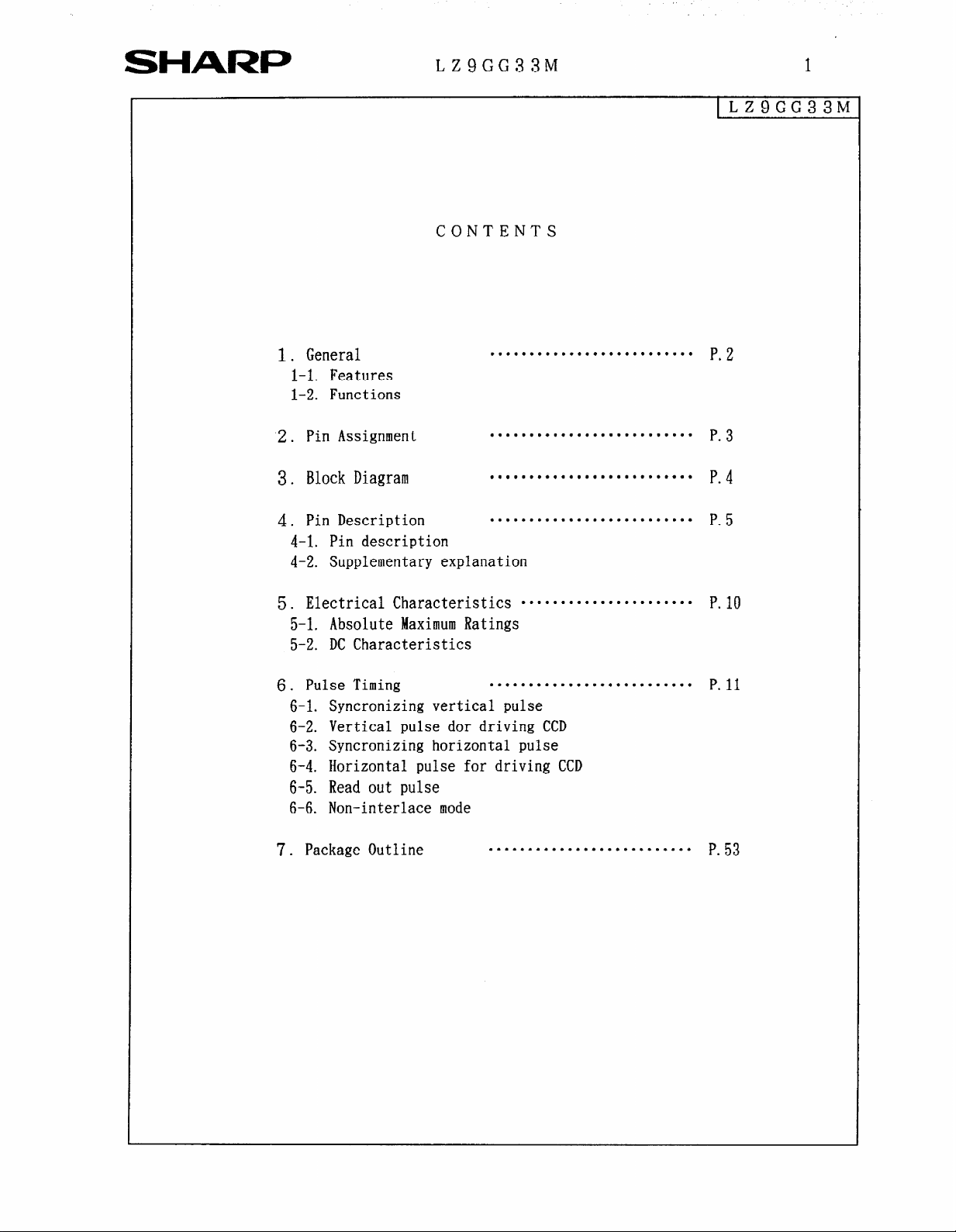
1. General
l-l. Features
l-2. Functions
2. Pin Assignment
3. Block Diagram
4. Pin Description
4-l.
Pin description
4-2. Supplementary explanation
5. Electrical Characteristics l *.*..******....*..*.. P.10
5-L Absolute Maximum Ratings
5-2. DC Characteristics
6 f Pulse Timing
6-l. Syncronizing vertical pulse
6-2. Vertical pulse dor driving CCD
6-3. Syncronizing horizontal pulse
6-4. Horizontal pulse for driving CCD
6-5. Read out pulse
6-6. Non-interlace mode
l t....**.*.~*****..~.*~...
. . . . . . . . . . . . . ..I..........
.**..****..*.*...........*
..,...****................
..*.***......,r***~......*
P. 2
P. 3
P. 4
P. 5
P. 11
7. Package Outline
. . ..+...*........****.*..*
P. 53
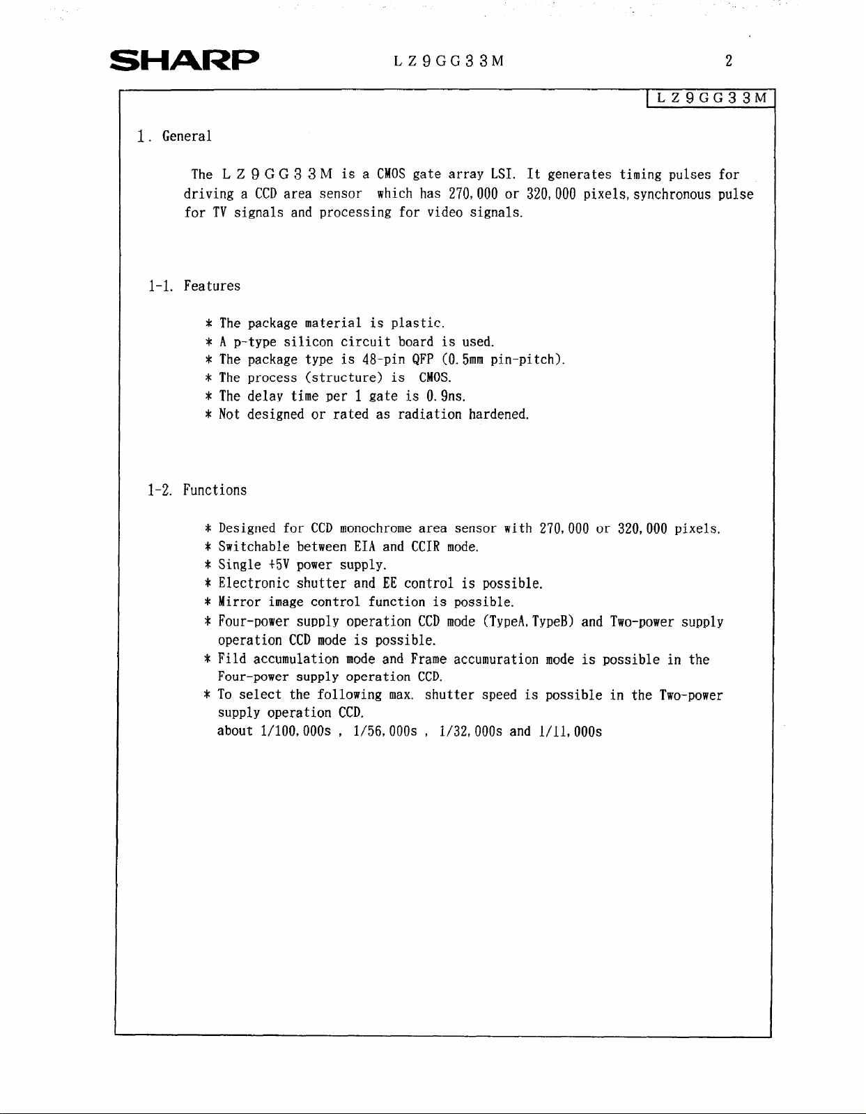
1. General
LZ9GG33M
1 LZ9GG33M
The LZ9GG33M
driving a CCD area sensor which has 270,000 or 320,000 pixels,synchronous pulse
for TV signals and processing for video signals.
l-l. Features
t The package material is plastic.
* A p-type silicon circuit board is used.
* The package type is 4%pin QFP (0.5mm pin-p
t The process (structure) is CMOS.
* The delay time per 1 gate is 0.9ns.
t Not designed or rated as radiation hardened.
1-2. Functions
$ Designed for CCD monochrome area sensor with 270,000 or 320,000 pixels.
I Switchable between EIA and CCIR mode.
* Single +5V power supply.
* Electronic shutter and EE control is possible.
* Mirror image control function is possible.
* Four-power supply operation CCD mode (TypeA,TypeB) and Two-power supply
operation CCD mode is possible.
* Fild accumulation mode and Frame accumuration mode is possible in the
Four-power supply operation CCD.
t To select the following max.
supply operation CCD.
about l/lOO,OOOs , 1/56,OOOs , 1/32,OOOs and l/ll,OOOs
is a CMOS gate array LSI. It generates timing pulses for
itch
1.
shutter speed is possible in the Two-power
SHARP
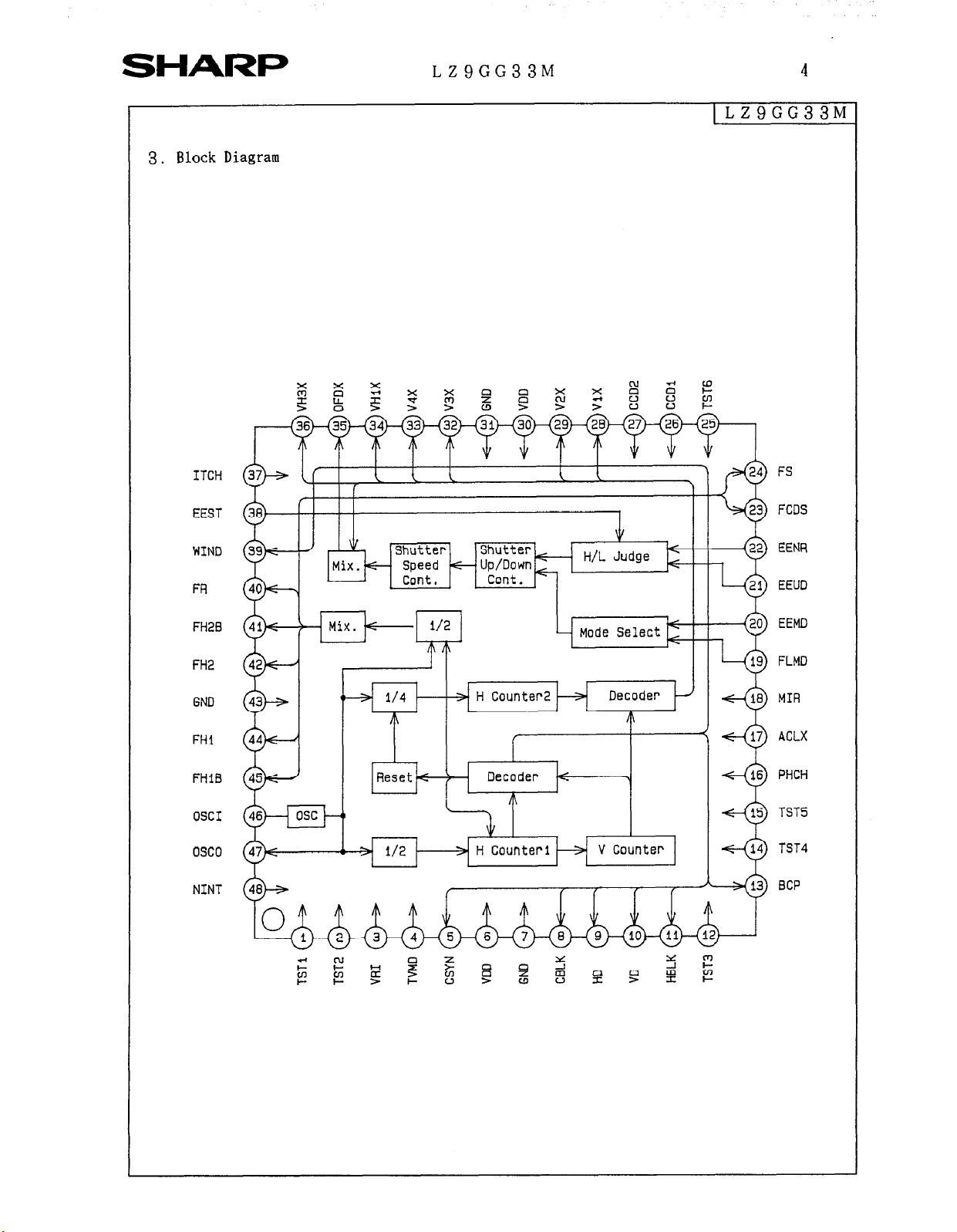
2. Pin Assignment
LZ9GG33M
ILZ9GG33M
IC : Input (CMOS level)
I cu : Input (CMOS level with pull-up resister)
I csu : Input (CMOS Schmitt-trigger level with pull-up resister)
ICD : Input (CMOS level with pull-down resister)
0 : output
06MA2 :Output
06MA3 :Output
ON : Output(N-ch open drain)
OSCI : Input pin for oscillation
osco
: Output pin for oscillation
SHARP
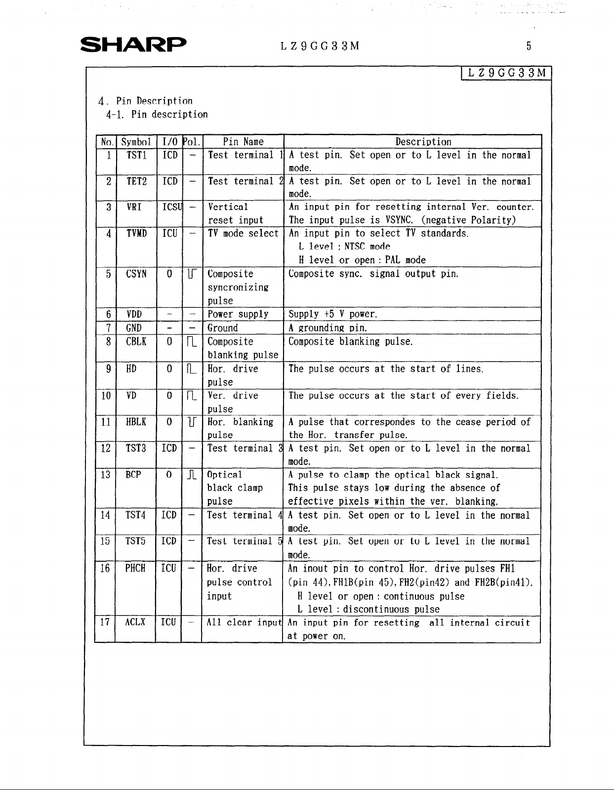
3. Block Diagram
ITCH
EEST
LZ9GG33M
4
1 LZ9GG33M
WIND
FR
FH2B
FH2
GND
FHI
FHlB
NINT @+-
,
l/4
m
Reset
f f f f
Decoder
LZ9GG33M
ILZ9GG33M
4.
Pin Description
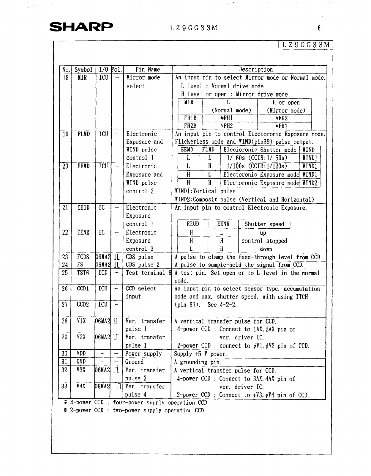
4-1. Pin description
No. Symbol I/O ‘01. Pin Name Description
1 TSTl
2 TET2
3 VRI ICSU - Vertical
4
TVMD ICU - TV mode select An input pin to select TV standards.
5 CSYN
6 VDD - - Power supply Supply +5 V power.
7
GND -
8 CBLK
9 HD 0 I-L Hor. drive
10 VD 0 /l- Ver. drive The pulse occurs at the start of every fields.
11 HBLK 0 u Hor. blanking A pulse that correspondes to the cease period of
12 TST3 ICD - Test terminal 3 A test pin. Set open or to L level in the normal
13 BCP 0 J-L Optical A pulse to clamp the optical black signal.
14 TST4 ICD - Test terminal 4 A test pin. Set open or to L level in the normal
15 TST5 ICD - Test terminal 5 A test pin. Set open or to L level in the normal
16 PHCH ICU - Hor. drive An inout pin to control Hor. drive pulses FHl
17 ACLX ICU - All clear input An input pin for resetting all internal circuit
ICD - Test terminal 1 A test pin. Set open or to L level in the normal
mode.
ICD - Test terminal 2 A test pin. Set open or to L level in the normal
mode.
An input pin for resetting internal Ver. counter.
reset input
0 r Composite
syncronizing
pulse
- Ground A grounding pin.
0 [-L Composite Composite blanking pulse.
blanking pulse
pulse
pulse
pulse the Hor. transfer pulse.
black clamp This pulse stays low during the absence of
pulse effective pixels within the ver. blanking.
pulse control (pin 44), FHlB(pin 45), FH2(pin42) and FH2Bcpin41).
input H level or open : continuous pulse
The input pulse is VSYNC. (negative Polarity)
L level; NTSC mode
H level or open : PAL mode
Composite sync. signal output pin.
The pulse occurs at the start of lines.
mode.
mode.
mode.
L level : discontinuous pulse
at power on.
SHARP
LZ9GG33M 6
ILZ9GG33M
No. Symbol I/O ‘01.
18 MIR
19 FLMD ICU - Electronic An input pin to control Electoronic Exposure mode
20 EEMD ICU - Electronic
21 EEUD IC
22 EENR IC
23 FCDS 36MA2 k CDS pulse 1 A pulse to clamp the feed-through level from CCD.
24 FS
25 TSTG ICD - Test terminal 6 A test pin. Set open or to L level in the normal
26 CCDl
27 CCD2 ICU - (pin 37). See 4-2-2.
ICU - Mirror mode
- Electronic An input pin to control Electronic Exposure.
- Electronic
36WA2 J-L CDS pulse 2 A pulse to sample-hold the signal from CCD.
ICU - CCD select An input pin to select sensor type, accumulation
Pin Name Description
An input pin to select Mirror mode or Normal mode
select L level : Normal drive mode
H level or open
MIR
(Normal mode) (Mirror mode)
FHlB =FHl *FHZ
FHZB
Exposure and Flickerless mode and WIND(pin39) pulse output.
WIND pulse
control 1
Exposure and
WIND pulse
control 2 WIND1:Vertical pulse
WIND2 : Composit pulse (Vertical and Horizontal)
Exposure
control 1 EEUD EENR Shutter speed
H L
Exposure H H control stopped
control 2 L H down
mode.
input
mode and max. shutter speed, with using ITCH
: Mirror drive mode
L
=FH2 *FHl
H or open
UP
28 VlX 36MA2 r Ver. transfer A vertical transfer pulse for CCD.
pulse 1 4-power CCD ; Connect to lAX, 2AX pin of
29 V2X 36MA2 r Ver. transfer
pulse 1 2-power CCD ;
30 VDD 31 CND - - Ground A grounding pin.
32 V3X 36MA2 n Ver. transfer
33 V4X 36MA2 fl Ver. transfer ver. driver IC.
c
I $-power CCD ; four-power supply operation CCD
% 2-power CCD ; two-power supply operation CCD
- Power supply Supply +5 V power.
A vertical transfer pulse for CCD.
pulse 3 $-power CCD ; Connect to 3AX,4AX pin of
pulse 4
2-power CCD ; Connect to 1V3, #V4 pin of CCD.
ver. driver IC.
connect to ,Vl,iVZ pin of CCD.
SHARP
LZ9GG33M
[LZ9GG33M
No. Symbol I/O pal.
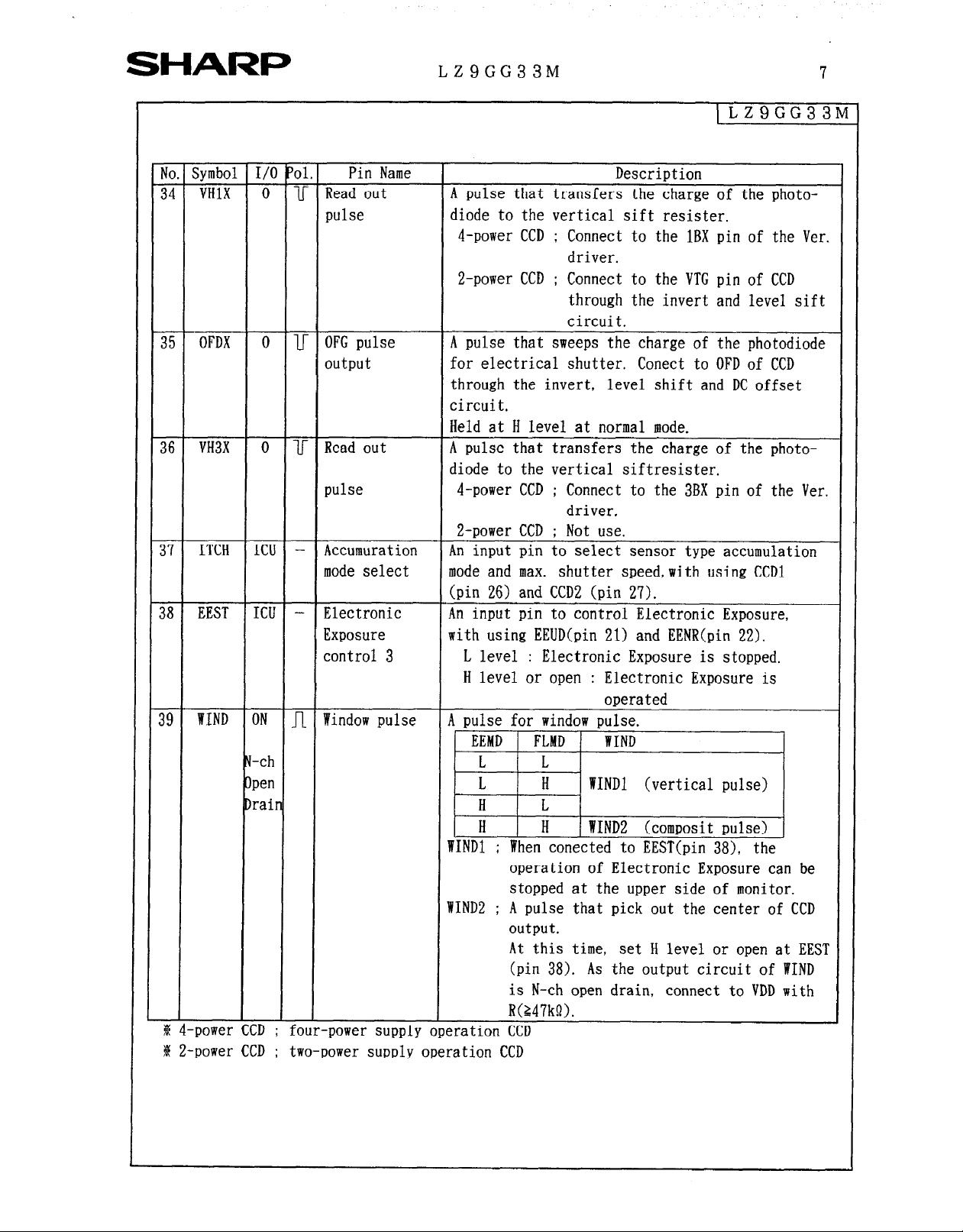
34 VHlX
35 OFDX 0 jJ OFG pulse A pulse that sweeps the charge of the photodiode
36 VH3X
37 ITCH ICU - Accumuration
38 EEST ICU - Electronic An input pin to control Electronic Exposure,
39 WIND ON n Window pulse
0 JJ- Read out A pulse that transfers the charge of the photo-
0 lJ Read out
Pin Name
pulse
output for electrical shutter. Conect to OFD of CCD
pulse q-power CCD ; Connect to the 38X pin of the Ver.
mode select mode and max. shutter speed,with using CCDl
Exposure
control 3 L level : Electronic Exposure is stopped.
diode to the vertical sift resister.
$-power CCD ; Connect to the 1BX pin of the Ver.
driver.
2-power CCD ; Connect to the VTG pin of CCD
through the invert and level sift
circuit.
through the invert, level shift and DC offset
circuit.
Held at H level at normal mode.
A pulse that transfers the charge of the photodiode to the vertical siftresister.
driver,
2-power CCD ; Not use.
An input pin to select sensor type accumulation
(pin 26) and CCDZ (pin 27).
with using EEUD(pin 21) and EENR(pin 22).
H level or open : Electronic Exposure is
A pulse for window pulse.
Description
operated
;;z,
I 4-power CCD ; four-power supply operation CCD
31t 2-power CCD ; two-power supply operation CCD
tij
WIND1 ; When conected to EEST(pin 381, the
operation of Electronic Exposure can be
stopped at the upper side of monitor.
WIND‘2 ; A pulse that pick out the center of CCD
output.
At this time, set H level or open at EEST
(pin 38). As the output circuit of WIND
is N-ch open drain, connect to VDD with
R(S47kB).
SHARP
No, Symbol I/O Pal. Pin Name Description
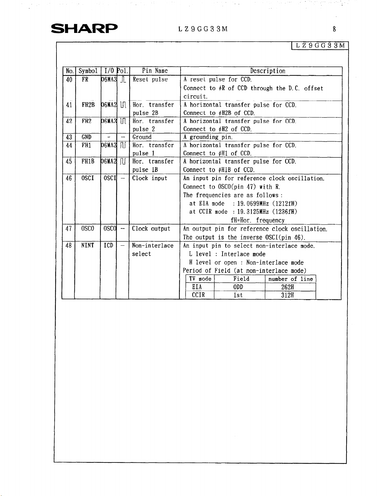
40 FR
41 FH2B 36MA2 lJ Hor. transfer A horizontal transfer pulse for CCD.
42 FH2 36MA3 m Hor. transfer A horizontal transfer pulse for CCD.
43 GND - - Ground
44 FH1 36MA3 m Hor. transfer A horizontal transfer pulse for CCD.
45 FHlB 36MA2 jlj Hor. transfer A horizontal transfer pulse for CCD.
46 OSCI OSCI - Clock input An input pin for reference clock oscillation.
47 OSCO OSCC - Clock output An output pin for reference clock oscillation,
48 NINT ICD - Non-interlace An input pin to select non-interlace mode.
L
36MA3
1 Reset pulse A reset pulse for CCD.
pulse 2B Connect to $HZB of CCD.
pulse 2 Connect to #HZ of CCD.
pulse 1 Connect to #Hl of CCD.
pulse 1B Connect to OHlB of CCD.
select L level :
LZ9GG33M
Connect to
circuit.
A grounding pin.
Connect to OSCO(pin 47) with R.
The frequencies are as follows :
at EIA mode
at CCIR mode : 19.3125MHz (1236fH)
The output is the inverse OSCI(pin 46).
H level or open : Non-interlace mode
Period of Field (at non-interlace mode)
TV mode Field number of line
EIA
CCIR
#R
of CCD through the D.C. offset
: 19.0699MHz (1212fH)
fH=Hor. frequency
Interlace mode
ODD 2628
1st 312H
8
(LZ9GG33M
SHARI=
LZ9GG33M
4-2. Supplementary explanation
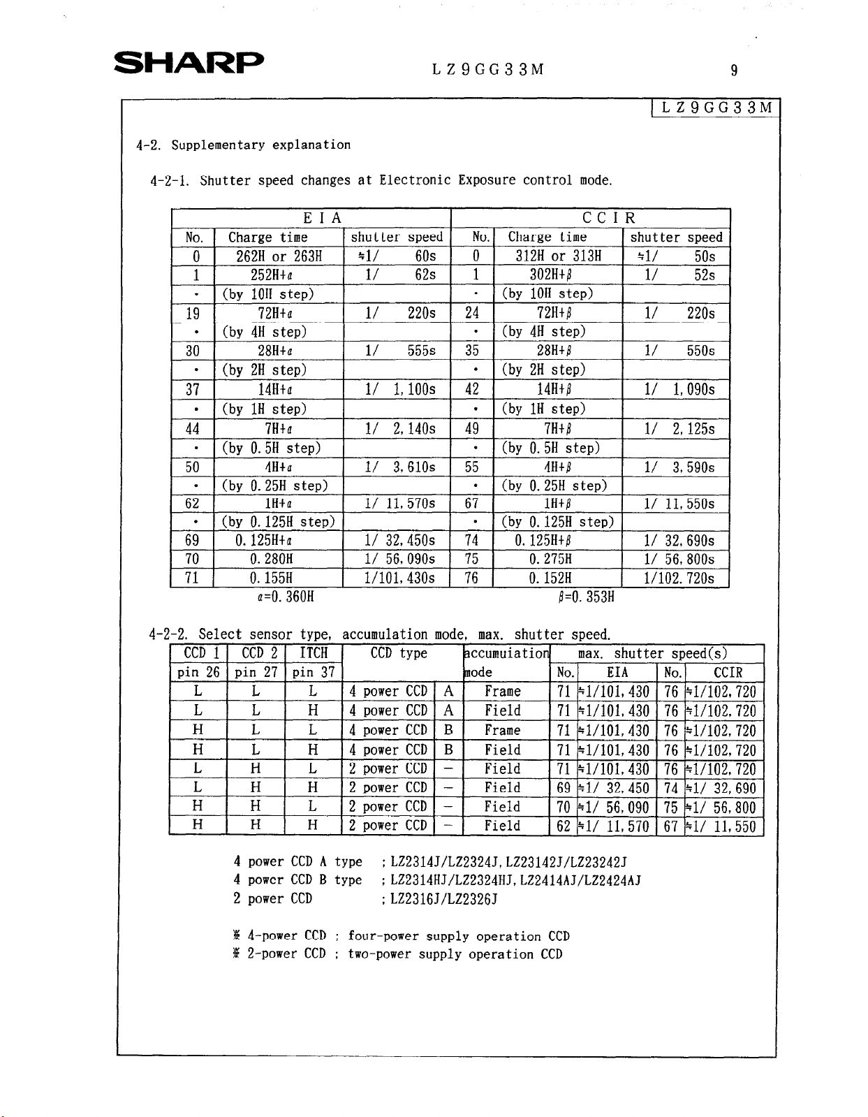
4-2-l. Shutter speed changes at Electronic Exposure control mode.
9
1 LZ9GG33M
l
(by 0.125H step)
69
0.125Hta
70 0.280H
71 0.155H
a=O. 360H
l/ 32,450s 7;
1/ 56,090s 75 0.275H l/ 56,800s
1/101,43Os 76 0.152H 1/102.720s
(by 0.125H step)
0.125Htb
8=0.3538
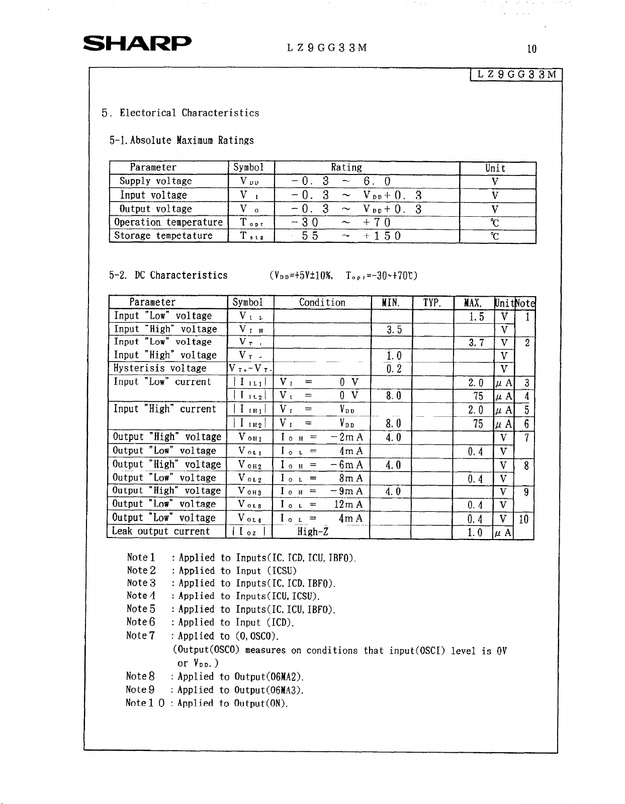
4-2-2. Select sensor type, accumulation mode, max. shutter speed.
4 power CCD A type
CCD
CCD
CCD
CCD
CCD
; LZ2314J/LZ2324J,LZ23142J/LZ232425
Field
Frame
Field
Field
Field
Field
Field
71 *l/101,430
71 =l/lOl, 430 76 +1/102,
69 =l/ 32,450 74 =l/ 32,
70 *l/ 56,090
62 =l/ 11,570
4 power CCD B type ; LZ2314HJ/LZ2324HJ, LZ2414AJ/LZ2424AJ
2 power CCD
; LZ2316J/LZ2326J
l/ 32,690s
76 *l/102,
75 *l/ 56,
67 =l/ 11,
I 4-power CCD
)g: 2-power CCD
; four-power supply operation CCD
; two-power supply operation CCD
.
.
SHARP
5.
Electorical Characteristics
5-l.Absolute Maximum Ratings
LZ9GG33M
10
iLZ9GG33M
Parameter
Supply voltage V
Input voltage
Output voltage v 0 -0.
Operation temperature T Opr
Storage tempetature T stB
5-2. DC Characteristics
Symbol Rating
DD
v I -0.
-0. 3 - 6. 0
3
- VDDf 0.
3
- VDDf 0.
-30
-55
- +70
-
U,,=t5VilO%, To,,=-30-t70t)
+150
Parameter Symbol Condition MIN. TYP.
Input
Input “High” voltage VI H 3. 5
“Low”
- -
voltage V 1 L
Input “Low” voltage VT +
Input “High” voltage VT -
Hysterisis voltage
Input “Low” current
VT+-VT- 0. 2
I 1 lLJvl= ov
I 1 ~1 Vr =
Input
Output
“High” current
“High” voltage
I 1
IH,t vl = VDD
( IIHZ~ VI =
0 V 8.0
VDD
I 0 H = -2mA 4.0
I I
1 0 L =
4mA 1
1. 0 V
8.0 75
I
3
3
1 I
Unit
V
V
V
“C
“C
MAX. kJni tvotl
1.5 v 1
3.7 v 2
2.0
,uA 3
75
fiA 4
2.0
/LA 5
PA 6
I
I n.4 Id
V
V
v
7
Note 1 : Applied to Inputs(IC,
ICD, ICU,
IBFO).
Note 2 : Applied to Input (ICSU)
Note 3 : Applied to Inputs(IC, ICD, IBFO).
Note 4
Note 5
Note 6
Note 7
Note 8
Note
Note1
: Applied to Inputs(ICU, ICSU).
: Applied to Inputs(IC. ICU, IBFO).
: Applied to Input (ICD).
: Applied to (0, OSCO).
(Output(OSCO) measures on conditions that input(OSC1) leve
or
VDD. >
: Applied to Output(OGMA2).
9
: Applied to Output(OGMA3).
0 : Applied to Output(
1 is
OV
v)
I
P
i3
u
-.----
,
,
: : :
---
-_-_.- _---mm-
NTSC
325 326 327 328 329 330 331 332 333 334 335 336 337
324
323
319 320 321 322
: : I I : : j i ; , , :
, :
I : j i : ; :
,
.--...-~
,
I : j
: :
n .wj
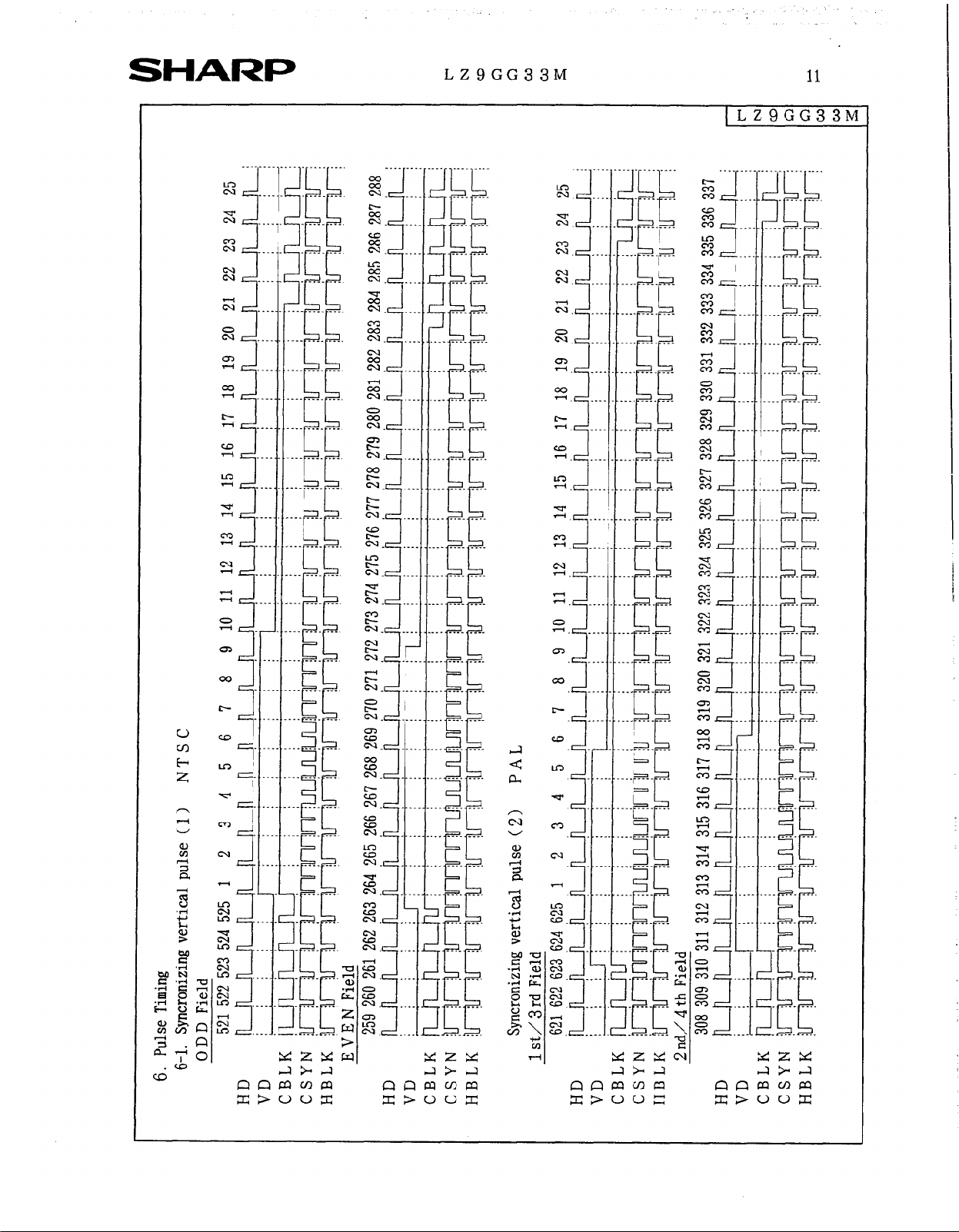
6-l. Syncronizing vertical pulse ( 1)
6. Pulse Timing
0 DD Field
HD
VD
CBLK
CSYN
E
-
HBLK
308 309 310 311 312 313 314 315 316 317 318
~n?lnn~~~~n~~~??~?~n~~~~~~~~~~~
i ; ;
!-I
CBLK n
HD
VD
SHARP
LZ9GG33M
i-$
I-
c
. . . . ..__....__
c
c
II
_. . . . . .
. . . .._..._
--...____.
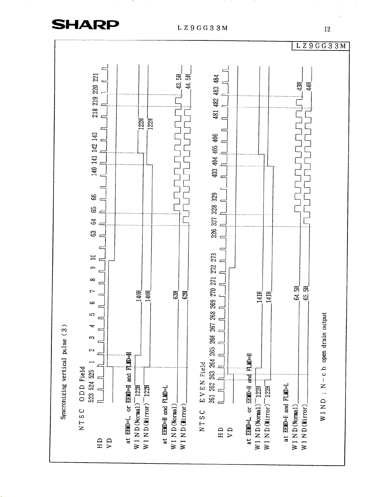
12
ILZ9GG33M
. .
. .
-.........____
. . . . . . .._..._.
3 E
.-......__
SHARI=
LZ9GG33M
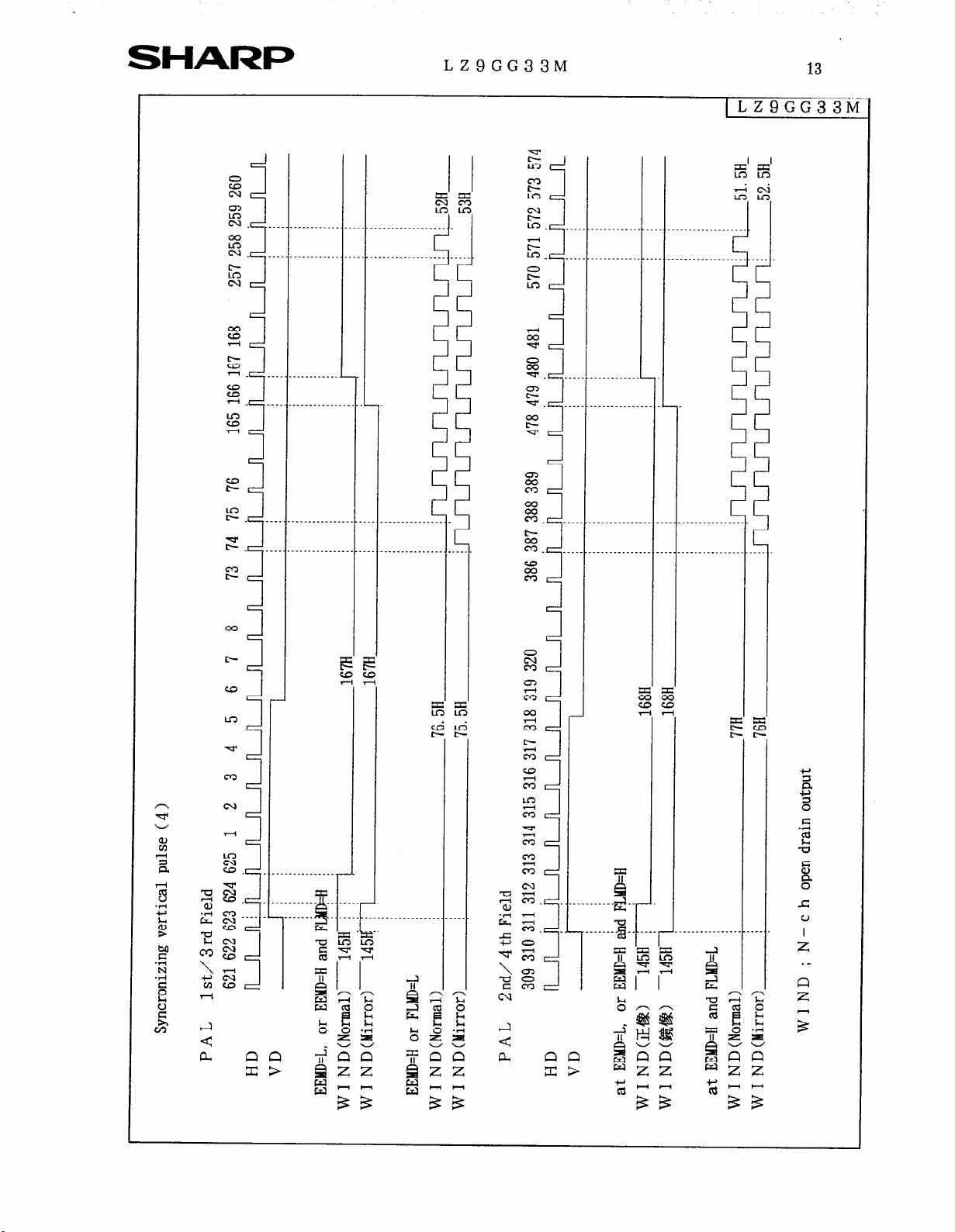
13
ILZ9GG33M
L.
. .
._.. .
_ _. _ . _ _. _
_ _ _ . _ _ _ . . .
,, ., .
,,
,“” . ,.
.” ,, . .
,,
287
286
285
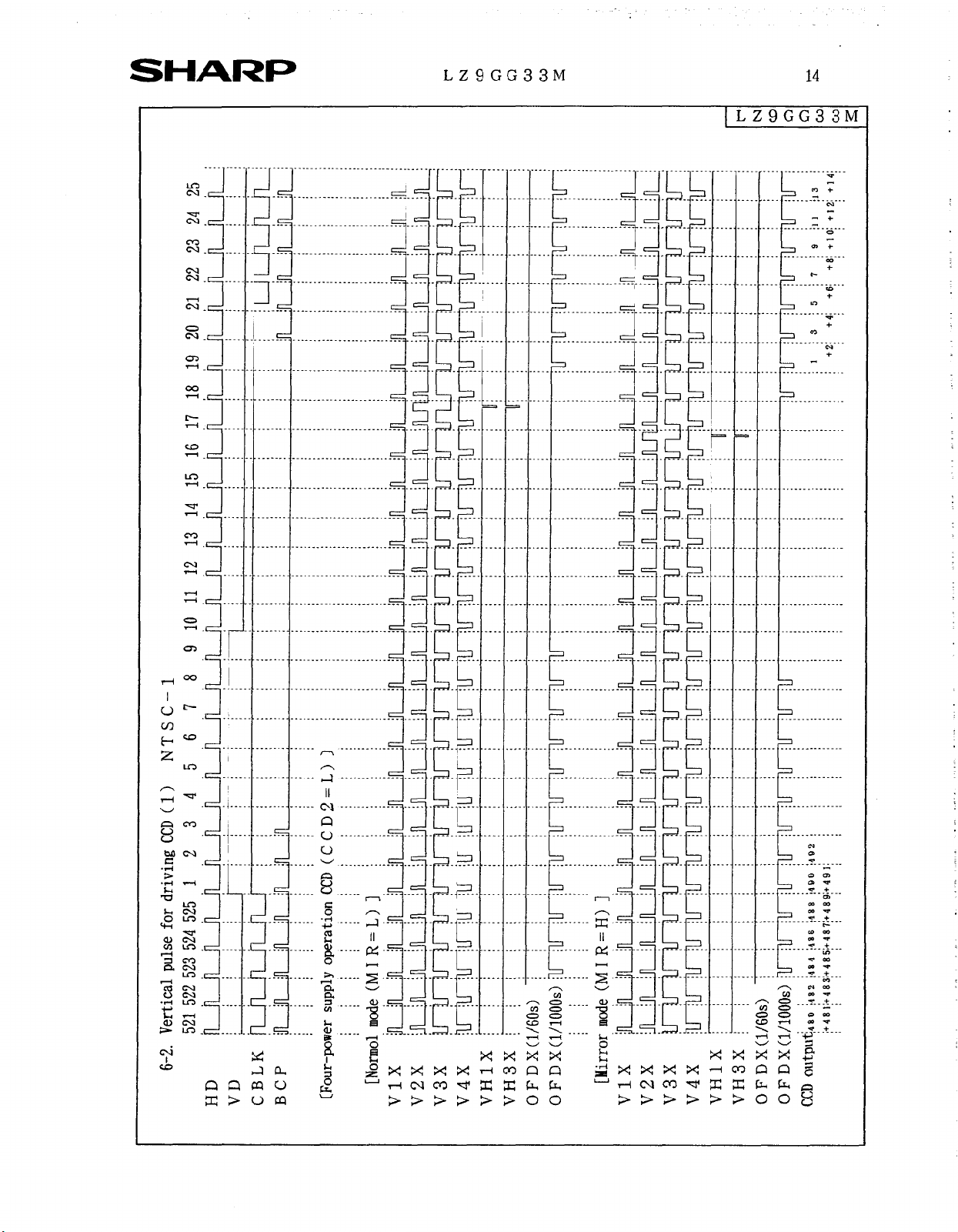
N T S C - 2
282 283 284
, , , , , ,
280 281
279
278
276 277
, ,,,
274 275
270 271 272 273
II,,
269
I
,, I., .
,, ,,
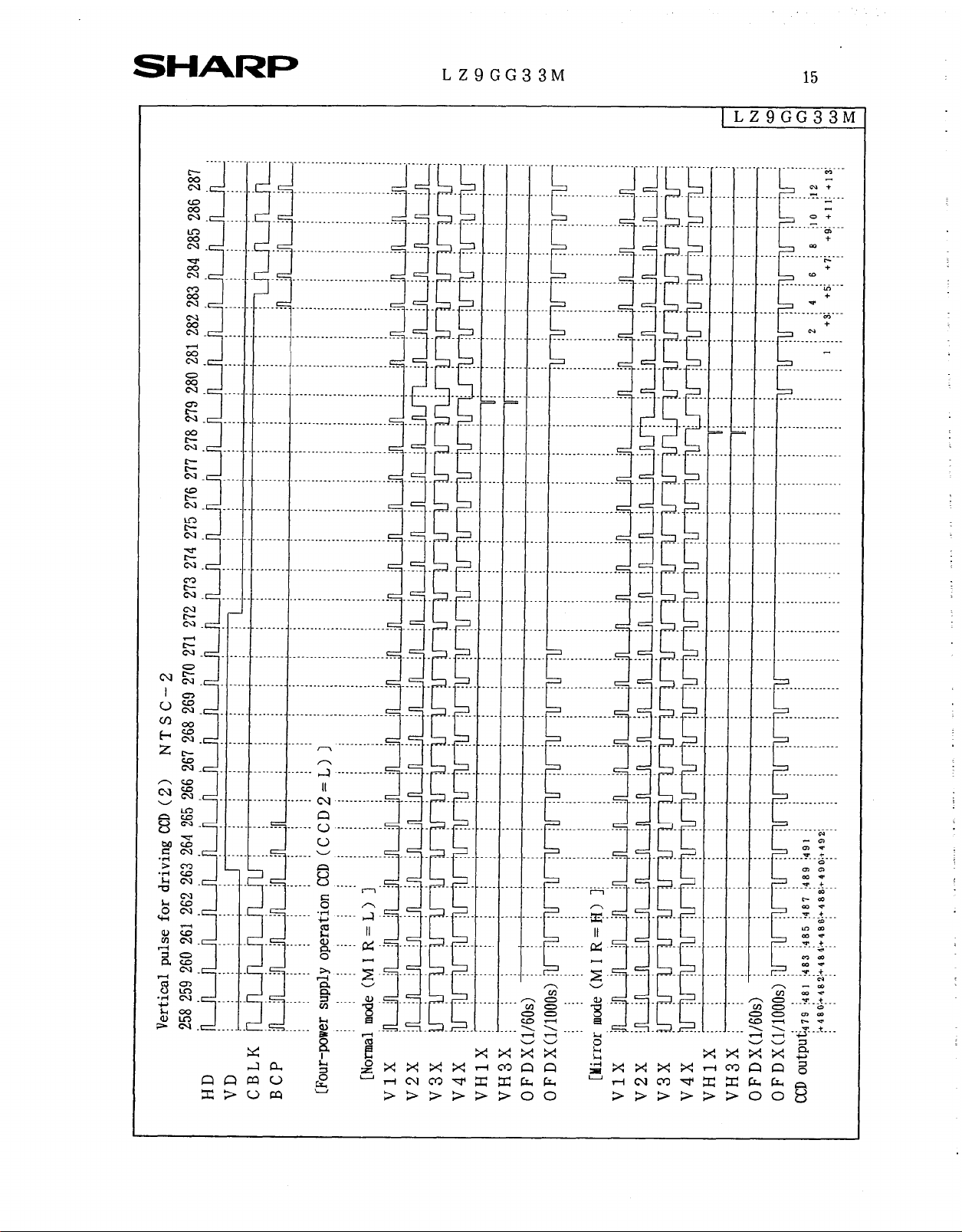
Vertical pulse for driving CCD (2 >
I I I.
I
260 261 262 263 264 265 266 267 268
259
258
III I
HD
.“” . ,.
,” ,, . .
,,,

NT S C - 4
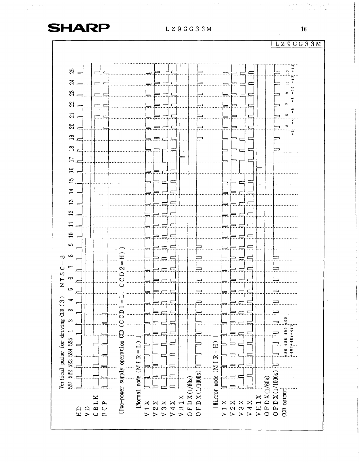
Vertical pulse for driving CCD (4 >
258 259 260 261 262 263 264 265 266 267

23 24
15 16 17 18 19 20 21 22
10 11 12 13 14
ll,llllll.ll,,,~
9
:
,-
1
. : : j
* I I
P A L - 1
Vertical pulse for driving CCD (5 >
6 7 8
’ ’ ’ ’ ’ ’ ’
620 621 622 623 624 625 1 2 3 4 5
,,III.IIIIIIIII
HD
VD I~i:iiIiii:::iiiii~:~::~iiiiiirii
VlX
v 2 x
v3x
v4x
VHlX
VHSX
OFDX(
-.
._ _
- ---- \_
in
in
in ;n

i
337
I ,, . , I , , ~
PAL-2
(6)
308 309 310 311 312 313 314 315 316 317 318 319 320 321 322 323 324 325 326 327 328 329 330 331 332 333 334 335 336
Vertical pulse for driving CCD
I I I I I I. I I . % I I I I < * <
HD
I I I I # , ,


 Loading...