SHARP
1 To : ED1
SPECIFICATIONS.
ISPEC No.
ISSUE:
Sep. 2 1999
Product Type
Model No.
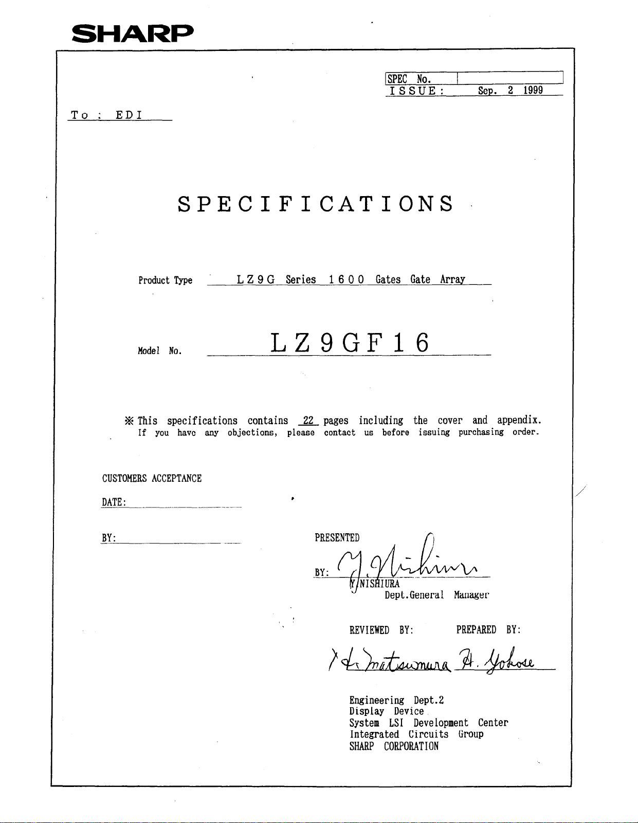
-X This specifications contains 22 pages including the cover and appendix.
If you have any objections, please contact us before issuing purchasing order.
CUSTOMERS ACCEPTANCE
DATE :
BY:
__-__---
_- --.-
LZ 9 G Series 1 6 0 0 Gates Gate Array
LZ9GFl6
PRESENTED
Dept.General Manager
REVIEWED BY:
Engineering Dept. 2
Display Device
System LSI Development Center
Integrated Circuits Group
SHARi CORPORATION -
PREPARED BY:
SHARP
LZ9GF16
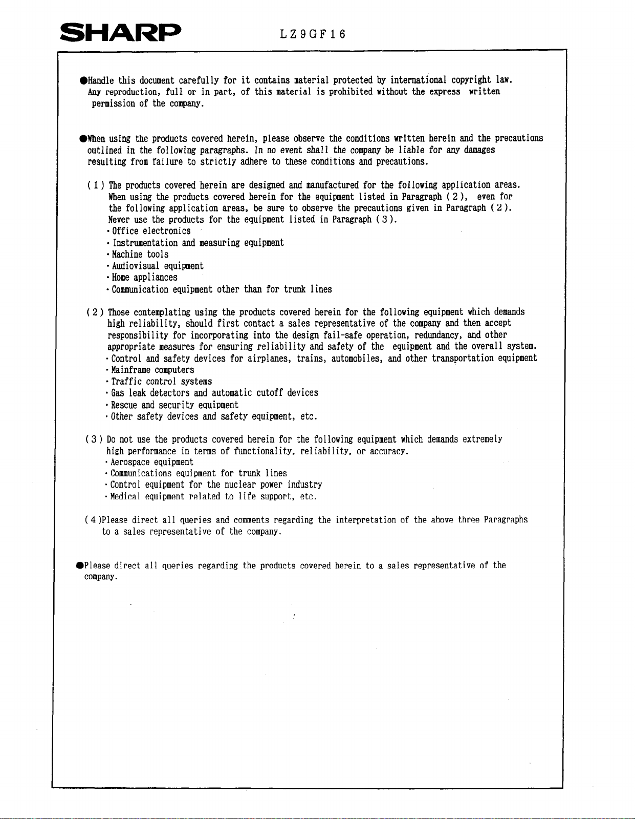
@Handle this document carefully for it contains material protected by international copyright law.
Any reproduction, full or in part, of this material is prohibited without the express written
permission of the company.
@When using the products covered herein, please observe the conditions written herein and the precautions
outlined in the following paragraphs. In no event shall the company be liable for any damages
resulting from failure to strictly adhere to these conditions and precautions.
( 1 ) The products covered herein are designed and manufactured for the following application areas.
When using the products covered herein for the equipment listed in Paragraph (2 1, even for
the following application areas, be sure to observe the precautions given in Paragraph ( 2 ).
Never use the products for the equipment listed in Paragraph ( 3 ).
*Office electronics
. Instrumentation and measuring equipment
l
Machine tools
* Audiovisual equipment
l
Home appliances
* Communication equipment other than for trunk lines
( 2 > Those contemplating using the products covered herein for the following equipment which demands
high reliability, should first contact a sales representative of the company and then accept
responsibility for incorporating into the design fail-safe operation, redundancy, and other
appropriate measures for ensuring reliability and safety of the equipment and the overall system.
. Control and safety devices for airplanes, trains, automobiles, and other transportation equipment
. Mainframe computers
. Traffic control systems
. Gas leak detectors and automatic cutoff devices
0 Rescue and security equipment
0 Other safety devices and safety equipment, etc.
( 3 ) Do not use the products covered herein for the following equipment which demands extremely
high performance in terms of functionality, reliability, or accuracy.
*Aerospace equipment
* Communications equipment for trunk lines
. ControI equipment for the nuclear power industry
*Medical equipment related to life support, etc.
( 4 )Please direct all queries and comments regarding the interpretation of the above three Paragraphs
to a sales representative of the company.
l Please direct all queries regarding the products covered herein to a sales representative of the
company.
LZ9GFi6
CONTENTS
1
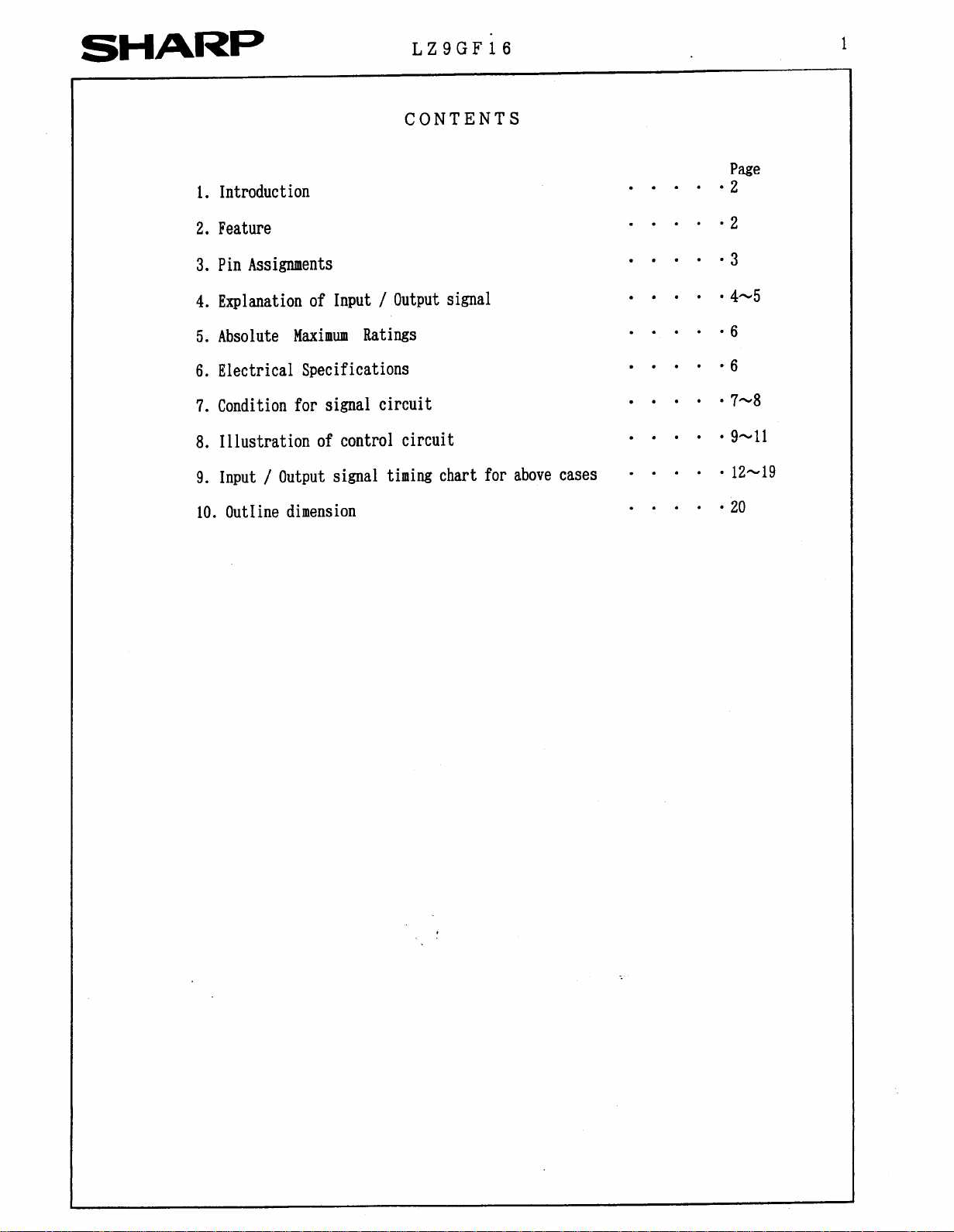
1. Introduction
2. Feature
3. Pin Assignments
4. Explanation of Input / Output signal
5. Absolute Maximum Ratings
6. Electrical Specifications
7. Condition for signal circuit
8. Illustration of control circuit
9. Input / Output signal timing chart for above cases
10. OutIine dimension
. . . .
. . . .
. . . .
. . . .
. . . .
. . . .
. . . .
. . . .
. . . .
. . . .
Page
02
92
l 3
l
4-5
-6
-6
l
7-8
l
9-11
’ 12-19
l
20
* SHARI=
1. Introduction
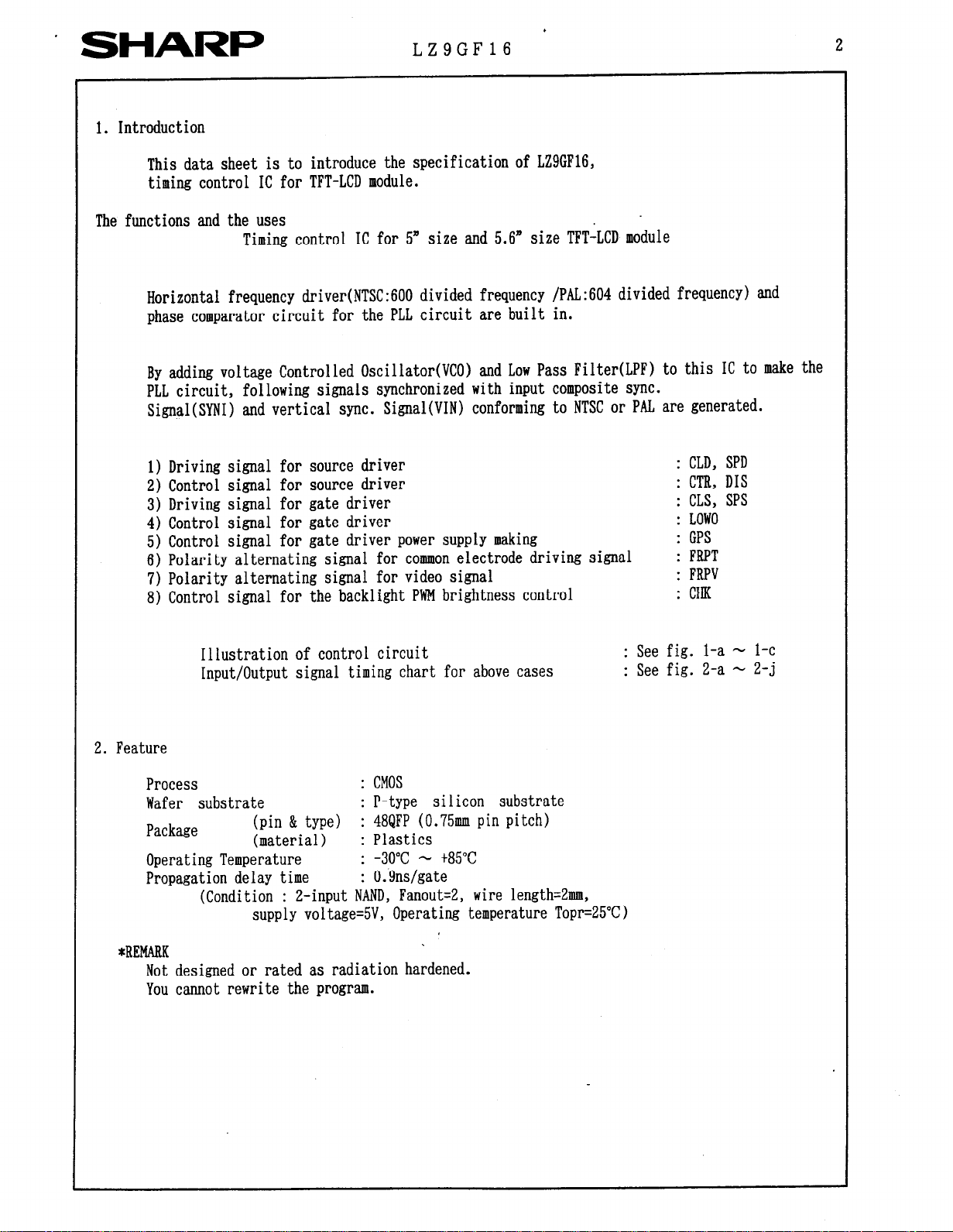
This data sheet is to introduce the specification of LZ9GF16,
timing control IC for TFT-LCD module.
The functions and the uses
Horizontal frequency driver(NTSC:600 divided frequency /PAL:604 divided frequency) and
phase comparator circuit for the PLL circuit are built in.
By adding voltage Controlled Oscillator(VC0) and Low Pass Filter(LPF) to this IC to make the
PLL circuit, following signals synchronized with input composite sync.
Signal(SYN1) and vertical sync. Signal(VIN) conforming to NTSC or PAL are generated.
.
LZ9GF16
Timing control IC for 5” size and 5.6” size TFTlLCD module
2
1) Driving signal for source driver
2) Control signal for source driver
3) Driving signal for gate driver
4) Control signal for gate driver
5) Control signal for gate driver power supply making
6) Polarity alternating signal for common electrode driving signal
7) Polarity alternating signal for video signal
8) Control signal for the backlight PWM brightness control
2. Feature
Process
Wafer substrate
Package
Operating Temperature : -30°C - +85”C
Propagation delay time
Illustration of control circuit
Input/Output signal timing chart for above cases
: CMOS
: P-type silicon substrate
(pin & type)
(material) : Plastics
(Condition
supply voltage=5V, Operating temperature Topr=25”C)
: Z-input NAND, Fanout=X, wire length=2mm,
: 48QFP (0.75mm pin pitch)
: 0. Snslgate
: CLD, SPD
: CTR, DIS
: CLS, SPS
: LOW0
: GPS
: FBPT
: FRPV
: CHK
: See fig. l-a - l-c
: See fig. 2-a - 2-j
*REMARK
Not designed or rated as radiation hardened.
You cannot rewrite the program.
SHARP
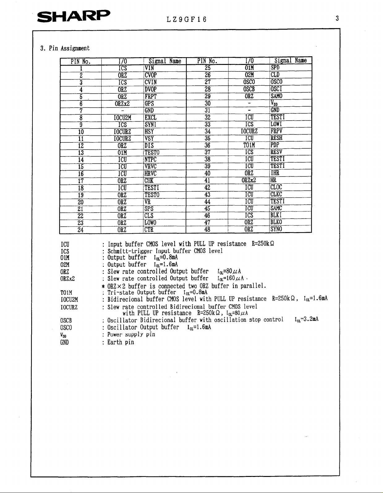
3. Pin Assignment
LZ9GF16
3
ICU
ICS
01M
02M
ORZ
ORZx2
TOlM
IOCUBM
IOCURZ
OSCB
osco
hD
GND
: Input buffer CMOS level with PULL UP resistance R=250k8
: Schmitt-trigger Input buffer CMOS level
: Output buffer I,=O.BmA
: Output buffer 1,,=1.61nA
: Slew rate controlled Output buffer
: Slew rate controlled Output buffer 1~,=16OflA .
* ORZx2 buffer is connected two ORZ buffer in parallel.
: Tri-state Output buffer 1,,,=0.8mA
: Bidirecional buffer CMOS level with PULL UP resistance R=250kQ, 1,~=1.6mA
: Slew rate controlled Bidirecional buffer CMOS level
with PULL UP resistance R=250kQ, IoL=80pA
: Oscillator Bidirecional buffer with oscillation stop control
: Oscillator Output buffer Io,=l.6mA
: Power supply pin
: Earth pin
I,,=BOfiA
10,=3. 2mA
SHARP
LZ9GF16
4
1
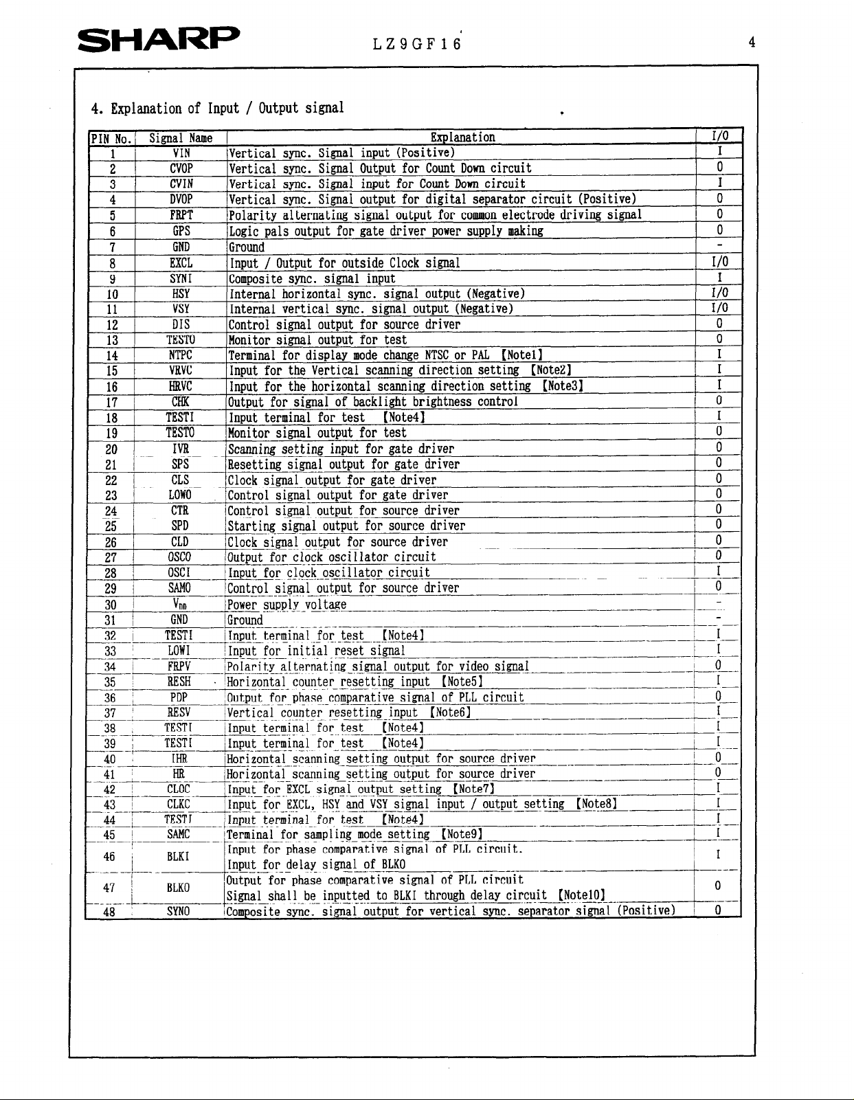
4. Explanation of Input / Output signal
?IN No.’
1 I
Signal Name
VIN Vertical sync. Signal input (Positive)
Explanation I/O
.
2 CVOP Vertical sync. Signal Output for Count Down circuit
3 CVIN Vertical sync. Signal input for Count Down circuit
4 DVOP Vertical sync. Signal output for digital separator circuit (Positive) 0
5
FBJT Polarity alternating signal output for common electrode driving signal 0
6 GPS Logic pals output for gate driver power supply making 0
7
a
GND
Ground
EXCL Input / Output for outside Clock signal
9 SYNI Composite sync. signal input
10 HSY Internal horizontal sync. signal output (Negative)
11 VSY Internal vertical sync. signal output (Negative)
12 DIS Control signal output for source driver
13
TEST0
Monitor signal output for test
14 NTPC Terminal for display mode change NTSC or PAL [Note11 I
15
16
17
ia
VRVC Input for the Vertical scanning direction setting (Note21
HRVC Input for the horizontal scanning direction setting (Note31
CHK Output for signal of backlight brightness control 0
TEST1
Input terminal for test (Note41
19 TEST0 Monitor signal output for test
20
21
22
23
24
25
26
27
28 ,
29 I
30 j
31 / GND I Ground
32 I
-__
33
---__
34
.__ -.- -
35 I
36 :
-~---
37 ’
_____.____~ __ ._~ ~..... ._ ~. .- __ ..-. ~-____-__
38
39 ; TEST1
_---
40 F---
.-.- ~~ A&y-:--.
41 ,Horlzontal scanning setting output for source driver
_-.------e-.---. --- -__--___
42 ~
IVB Scanning setting input for gate driver
_--
SPS Besetting signal output for gate driver
CLS
Clock signal output for gate driver
.__.
LOW0 Control signal output for gate driver 0
CT& Control signal output for source driver
--__
_____-
SPD Starting signal output for source driver
CLD Clock signal output for source driver
osco
osc I Input for clock oscillator circuit
SAM0 Control signal output for source driver
~----t---------.~... --.. ~__
bD
TEST1
7---./Input-f;;-ini fil ye;;7-;j-ga1
LOW1
--F-~~--~-‘--.-..-
__--_- _.-
Output for clock oscillator circuit
_---_ .---
..___- --._- . .._--.- ___IPower supply voltage
_ ._ ..-. -~- -- -..__--__ ~-______
f--------;. _- ---- --
IInput terminal for test(Note41
-
~~~--~
-____
-__
-__-
IPoIarlty alternating<ign&%$ut for video signa
RESH TGi%t!l-counter resetting input (Note51
PDP 1 o-
IOutput for_phasecomparative signal of PLL circuit
--.--
RESV /Vertical counter resetting input (Note61
TEST1 Input terminal for test (Note41
-I-
__-.._ . ~.---- ____---
IInput terminal for test (Note41
___. -_- .-. --.-__-__ -_.~
iHorizontal scanning setting output for source driver
- -.-.
_-__--~-~
-__
-------------,~ -
--j--‘-t
--
___-
CLOC
Input for EXCL si&l-outpu%etting (Note71
____
1-- --
--i--t-
VSY signal input / output setting (Note81
I
0
I
I/O
I
I/O
I/O
0
0
I
I
I
0
0
0
0
0
/ 0
/ I
_.-
-L--I .-
SHARF=
LZ9GF16
.
5
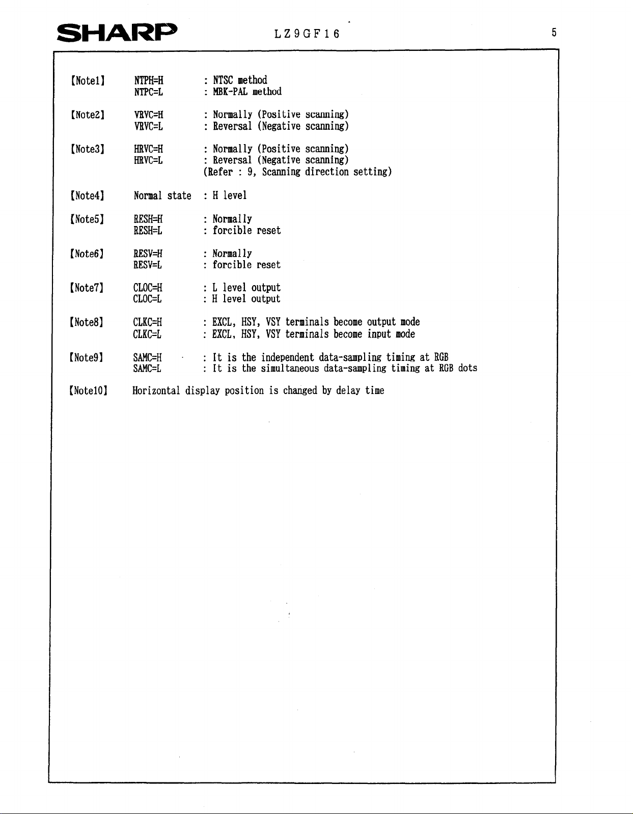
(Note11
(Note21
[Note31
(Note41
(Note51
[Note61
(Note71
(Note81
(Note91
NTPH=H
NTPC=L
VRVC=H
VRVC=L
HRVC=H
HRVC=L
Normal state : H level
BESH=H
RESH=L
RESV=H
RESV=L : forcible reset
CLOC=H : L level output
CLOC=L
CLKC=H
CLKC=L
SAMC=H : It is the independent data-sampling timing at RGB
SAMC=L
: NTSC nethod
: MBK-PAL method
: Normally (Positive scanning)
: Reversal (Negative scanning)
: Normally (Positive scanning)
: Reversal (Negative scanning)
(Refer : 9, Scanning direction setting)
: Normally
: forcible reset
: Normally
: H level output
: EXCL, HSY, VSY terminals become output mode
: EXCL, HSY, VSY terminals become input mode
: It is the simultaneous data-sampling timing at RGB dots
(Note101
Horizontal display position is changed by delay time
 Loading...