

Sharp LH540205D-35, LH540205D-20, LH540205D-50, LH540205D-25 Datasheet
LH540205
CMOS 8192 × 9 Asynchron ous FIFO
FEATURES
•• Fast Acces s Times : 20/25/ 35/ 50 ns
•• Fast- Fall-Through Time Ar chitect ure Based on
CMOS Dual-Port SRAM Tec hnology
•• Input Port and Output Port Have Entirely
Indepen dent Timing
•• Expandable in Width and Depth
•• Full, Half-Full, and Empty Status Flags
•• Data Retransmission Capability
•• TTL-Compa tible I/O
•• Pin and Functiona lly Compatible with Am/IDT72 05
•• Cont rol Signals Ass ertive- LOW for No ise Immunit y
•• Package: 28-Pin, 300-mil PDIP
FUNCTIONAL DESCRIPTION
The LH540205 is a FIFO (First-In, First-Out) memory
device, bas ed o n fully-stat ic CMO S dual-port SRAM tec hnology, capable of storing up to 8192 nine-bit words. It
follows the industry-standard architecture and package
pinouts for nine-bit asynchronous FIFOs. Each nine-bit
LH540205 wor d may consist of a standar d e ight-bit by te,
toget her with a parit y bit or a block-mark in g/fr am ing bit.
The input and output ports operate entirely inde-
pendently of each other , unless the LH540205 becomes
either tota lly full or else totally empty. Data flow at a port
is initiated by asserting either of two asynchronous, assertiv e-LOW contr ol input s: W rite ( W) f or dat a ent ry at the
input por t, or Read (R ) for data retrieval at the output port.
Full, Half-Full, and Empty status flags monitor the
extent to which the internal memory has been filled. The
system may make use of these status outputs to avoid
the risk of data loss, which otherwise might occur either
by attempt ing to write additiona l words into an alrea dy-full
LH540205, or by attempting to read additional words from
an already-empty LH540205. When an LH540205 is
operating in a depth-cascaded configuration, the Half-Full
Flag is not available.
Data words are read out from the LH540205’s output
port in precisely the same order that they were writt en in
at its input port; that is, accord ing to a First-I n, First Out
(FIFO ) queu e discipline. Since the addr essing sequ ence
for a FI FO device’s memory is internally predefined, no
external addr essin g informa tion is required for the operation of the LH540205 device.
Drop-in-replacement compatibility is maintained with
both larger sizes and smaller sizes of industry-standard
nine-bit asynchronous FIFOs. The only change is in the
number of internally-stored data words implied by the
states of the Full Flag and the Half- Full Fla g.
The Retra nsmit (RT) control signal caus es the internal
FIFO -memory -a rray read- addr ess point er to be set back
to zero, to point to the LH540205’ s first physical me mory
location , without affecting the internal FIFO-memoryarra y write- addr ess p oint er. Th us, t he Ret ransm it c ont ro l
signal provides a mechanism w hereby a block of data,
delimited by the zero physical address and the current
write-address-pointer value, may be read out
repeatedly
an arbitr ary number of times. The only restrict ions ar e that
neither the read-address pointer nor the write-address
point er may ‘wr ap ar ou n d’ dur ing t his e ntir e pro c ess, i.e. ,
advance past physical location zero after traversing the
entire memory. The retransmit facility is not avai lable
when an LH5 40205 is ope rating i n a depth-expanded
configura tion.
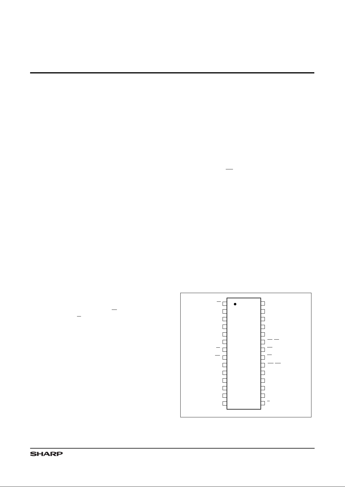
PIN CONNECTIONS
540205-2D
1
2
3
4
5
6
7
8
9
10
11
12
13
14
W
D
8
D
3
D
2
D
1
D
0
XI
FF
Q
0
Q
1
Q
2
Q
3
Q
8
V
SS
28
27
26
25
24
23
22
21
20
19
18
17
16
15
D
7
FL/RT
RS
EF
XO/HF
Q
5
Q
4
R
Q
6
Q
7
D
6
D
5
D
4
V
CC
28-PIN PDIP TOP VIEW
Figure 1. Pin Conn ections for PDIP Packages
1
The Reset (RS) control si gnal returns the LH540205
to an initial state, empty and ready to be filled. An
LH540205 should be reset during ever y system power-up
sequence. A reset operation causes the internal FIFOmemor y-array write-addr ess point er , as well as the readaddress pointer, to be set back to zero, to point to the
LH540205’s firs t physica l memor y location . Any inf ormation which previously had been stored within the
LH540205 is not recoverab le after a reset operation.
A ca scading (dept h-expansion) sc heme may be implemented by using the Expansion In (XI) i nput signal and
the Expansion Ou t (XO/HF) output signal. This scheme
allows a deeper ‘effective FIFO’ to be implemented by
using two or more indiv idual LH540205 devices, without
incurring additional latency (‘fallthrough’ or ‘bubblethrough’) delays, and without the necessity of storing
and ret rieving an y given data word more than onc e. In this
cascaded operating mode, one LH540205 device must
be designated a s the ‘first-load’ or ‘master’ device, by
grounding its First-Load (FL/RT ) control input; the remaining LH54 0205 devices are designat ed as ‘slaves, ’ by tying
their FL/RT input s HIGH. Because of the need to share
contro l signals on pins, the Half-Full Flag and the r etran smission capability are not available for either ‘master’ or
‘sla ve’ LH5402 05 devices oper at ing in c asca ded mod e.
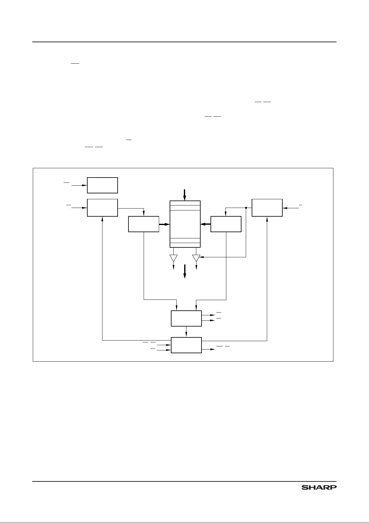
FUN CTIONAL DESCRIPTION (con t’d)
DATA OUTPUTS
Q
0
- Q
8
FLAG
LOGIC
EXPANSION
LOGIC
WRITE
POINTER
INPUT
PORT
CONTROL
READ
POINTER
DATA INPUTS
D
0
- D
8
DUAL-PORT
RAM
ARRAY
8192 x 9
R
W
XO/HF
XI
FL/RT
EF
FF
. . .
540205-1
RESET
LOGIC
RS
OUTPUT
PORT
CONTROL
Figure 2. LH540205 Block Diagram
LH540205 CMOS 8192 × 9 Asynchronous FIFO
2

OPERATIONAL DESCRI PT ION
Reset
The LH540 205 is r eset whenever the Reset input (RS)
is taken LO W. A re set operation initializes bot h the readaddress pointer and the write- add res s point er to point to
location zero, t he firs t physical memo ry l ocation. During
a reset operation, the state of the XI and FL/RT inputs
determines whethe r the device is in standalone mode or
in depth-cascaded mode. (See Tables 1 and 2 .) The
reset operation forces th e Emp ty Flag EF to be asserted
(EF = LOW), and t he Half-Full Flag HF and the Full Flag
FF to be de assert ed (HF = FF = HIGH); the Data Out pins
(D0 – D8) are for ced int o a high-im peda nce st ate.
A reset oper at ion is required whenever t he LH540 205
first is powered up. The Read (R) and Write (W) inputs
may be in any state when the re set oper ation is initiat ed;
but they must be HIGH, before the reset operation is
terminated by a rising edge of RS, by a time t
RRSS
(for
Read) or t
WRSS
(for Write) respectively. (See Figure 9 .)
Write
A write cycle is initiated by a falling edge of the Write
(W) contr ol input . Data setup times and hold times must
be observed for the data i nputs (D0 – D8). Write operations may occur independently of any ongoing read operation s. However , a write operat ion is possible only if the
FIFO is not full, (i. e., if the Fu ll Flag FF is HIGH).
At the fa lling e dge of W for the first write o peration after
the memory is half filled, the Half-Full Flag is asserted
(HF = LOW). It remains asserted until the difference
between the write pointer and the read pointer indicates
that the data words remaining in the LH540205 are filling
the FIFO memory to less than or equal to one-half of its
total capacity. The Half-Full Flag is deasserted
(HF = HIGH) by the appropriate rising edge o f R. (See
Table 3.)
The Full F lag is as serted (FF = LOW) at the falling edge
of W for the write operation which fills the last available
location in the FIFO mem ory a rray. FF = LOW inhibits
further write oper ations until FF is cleared by a v al id r ead
operation. The Full Flag is deasser ted (FF = HIGH) after
the next rising edge of R releases anot he r mem ory lo cation. (See Table 3.)
Read
A read cycle is initiated by a falling edge of the Read
(R) control input. Read data becomes valid at the data
output s (Q0 – Q8) after a time tA from the falling e dge of
R. After R goes HIGH, the data outputs return to a
high-impedance stat e. Read oper ations m ay occur in dependently of any ongoing write operations. However, a
read operation is possible only i f the FIFO is not empty
(i.e., if the Empty Flag EF is HIGH).
The LH540205’s in ternal read -ad dress and wri teaddres s point er s oper ate in suc h a way that con secut ive
read operations always access data words in the same
order that they wer e written . The Empty Flag is asse rted
(EF = LOW) after that falling edge of R which accesses
the last available data word in the FIFO memory. EF is
deasserted (EF = HIGH) after th e next rising edge of W
loads another valid data word. (See Table 3.)
Data Flow-Through
Read-data flow- throu gh mode occurs when the Read
(R) cont rol inpu t is brought LOW while the FIFO is empty ,
and is held LOW in antic ipation of a write cycle. At the end
of the next write cycle, the Empty F lag EF momentarily is
deasserted, and the data word just written becomes
available at the data outputs (Q0 – Q8) after a maximum time of t
WEF
+ tA. Additional write operations may occur
while the R input remains LOW; but only data from the
first write operation flows through to the data outputs.
Additional data words, if any, may be accessed only by
toggling R.
Write-data flow-through mode occurs when the Write
(W) input is brought LOW while t he FIFO is full, and is
held LOW in anticipation of a read cycle. At the end of the
read cycle, the Full Flag momentarily is deasserted, but
then immediately is reasserted in response to W being
held LOW. A data word is written into the FIFO on the
rising edge of W, which may occur no sooner than
t
RFF
+ t
WPW
after the read oper ation.
PIN DESCRIPT IONS
PIN PIN TYPE
1
DESCRIPTION
D0 – D
8
I
Input Data Bus
Q0 – Q
8
O/Z
Out put Data Bu s
W
I
Write Request
R
I
Read Request
EF
O
Empt y Flag
FF
O
Full Flag
PIN PIN TYPE
1
DESCRIPTION
XO/HF
O
Expansion Out/Half-Full Flag
XI
I
Expansion In
FL/RT
I
First Load/ Retransmit
RS
I
Reset
V
CC
V
Positive Power Supply
V
SS
V
Ground
NOTE:
1. I = Input, O = Output, Z = High-Impedance, V = Power Voltage Level
CMOS 8192 × 9 Asynchronous FIFO LH540205
3
OPERATIONAL DESCRIPTION (cont’d)
Retransmit
The FIFO can be made to reread previously-read data
by means of the Retransmit function. A retransmit operation is initiated by pulsing the
RT input LOW. Both R and
W must be deasserted (HIGH) for the duration of the
retransmit pulse. The FIFO’s internal read-address
pointer is reset to point to location zero, the first physical
memory location, while the internal write-address
pointer remains unchanged.
After a retransmit operation, those data words in the
region in between the read-address pointer and the
write-address pointer may be reaccessed by subsequent
read operations. A retransmit operation may affect the
state of the status flags
FF, HF, and EF, depending on
the relocation of the read-address pointer. There is no
restriction on the number of times that a block of data
within an LH540205 may be read out, by repeating the
retransmit operation and the subsequent read operations.
The maximum length of a data block which may be
retransmitted is 8192 words. Note that if the write-address
pointer ever ‘wraps around’ (i.e., passes location zero
more than once) during a sequence of retransmit operations, some data words will be lost.
The Retransmit function is not available when the
LH540205 is operating in depth-cascaded mode,
because the
FL/RT control pin must be used for first-load
selection rather than for retransmission control.
Table 1. Grouping-Mode Determination
During a Reset Operation
XI
FL/
RT
MODE
XO/HF
USAGEXIUSAGE
FL/RT
USAGE
H 1H
Cascaded
Slave
2
XO XI FL
H
1
L
Cascaded
Master
2
XO
XI FL
L
X
Standalone
HF (none) RT
NOTES:
1. A reset operation forces
XO HIGH for the nth FIFO, thus forcing
XI HIGH for the (n+1)st FIFO.
2. The terms ‘master’ and ‘s lave’ refer to operation in depth-cas-
caded groupin g m ode.
3. H = HIGH; L = LOW; X = Don’t Care.
Table 2. Expansion-Pin Usage Acco rding t o
Grouping Mode
I/O PIN
STANDALONE
CASCADED
MASTER
CASCADED
SLAVE
I
XI Grounded
From
XO
(n-1st
FIFO)
From XO
(n-1st
FIFO)
O
XO/HF
Becomes
HF
To
XI
(n+1st
FIFO)
To XI
(n+1st
FIFO)
I
FL/RT
Becomes
RT
Grounded
(Logic
LOW)
Logic
HIGH
Table 3. Status Flags
NUMBER OF UNREAD DATA
WORDS PRESENT WITHIN
8192 × 9 FIFO
FF HF EF
0HHL
1 to 4096 H H H
4097 to 8191 H L H
8192 L L H
LH540205 CMOS 8192 × 9 Asynchronous FIFO
4
OPERATIONAL MO DES
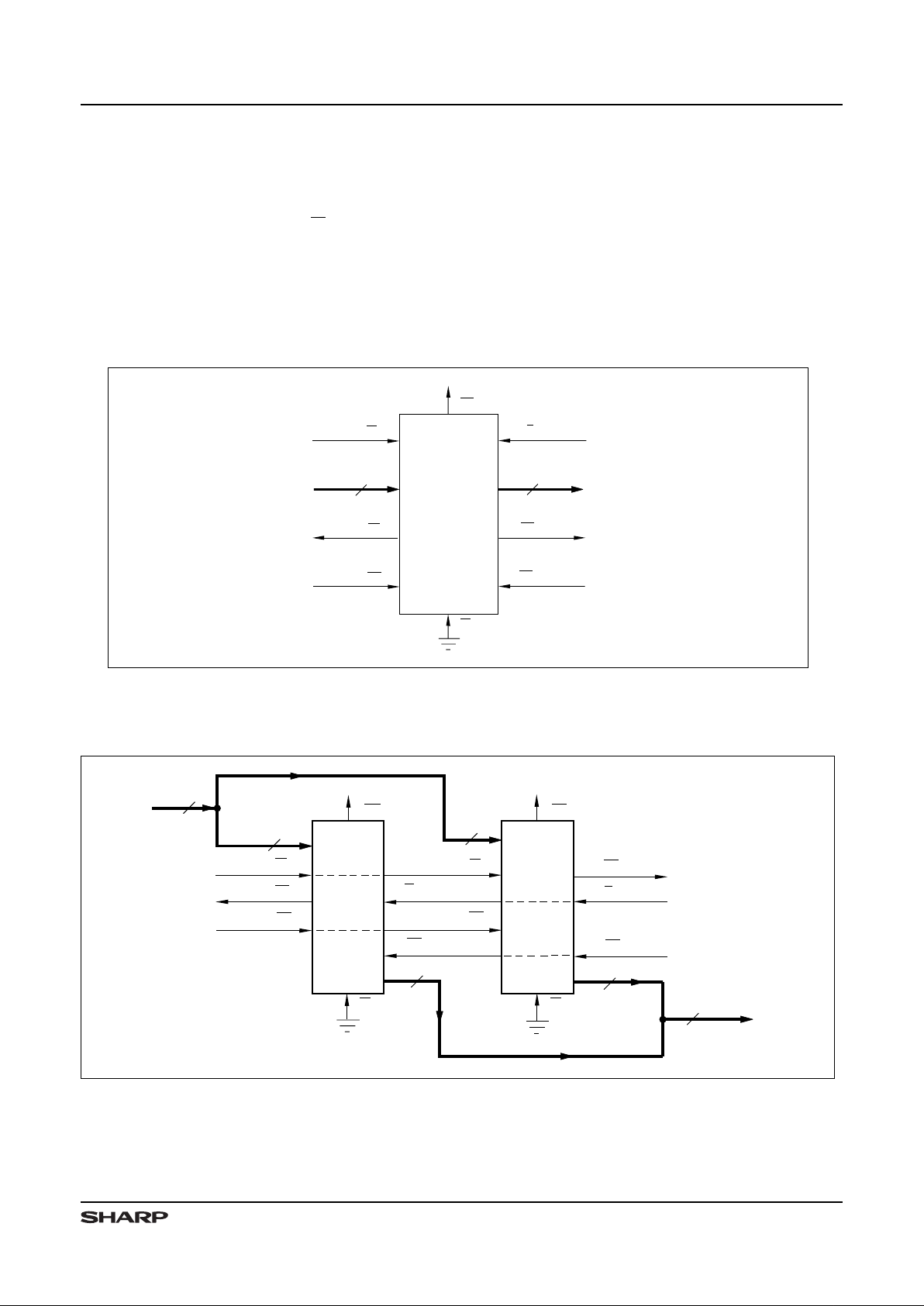
Standalo n e Configuration
When depth cascading is not required for a given
application, the LH540205 is placed in st anda lone mode
by tying the Expansion In input (XI) to ground. This
input is interna lly sampled during a reset operatio n. (See
Table 1.)
Width Expansion
Word -width expansion is imp lemented by placing multiple LH540205 devices in parallel. Each LH540205
should be configured for standalone mode. In this arrangem ent, the behavior of the status flags is ident ical for
all devices; so, in principle, a representative value for
each of these flags could be der ived from any one device .
In practice , it is better to derive ‘composite’ flag values
using external logic, since there may be minor speed
variatio ns between differe nt actual devices. (See Figures
3 and 4.)
WRITE
DATA IN
D
0
- D
8
9
FULL FLAG
RESET
XI
RT
RETRANSMIT
EMPTY FLAG
9
READ
HF
LH540205
W
FF
RS
R
EF
DATA OUT
Q
0
- Q
8
540205-17
Figur e 3. Standalone FI FO (8192 × 9)
18
WRITE
FULL FLAG
RESET
9
READ
EMPTY FLAG
R
EF
XI
RT
R
W
540205-18
RS
RETRANSMIT
RT
XI
HF
W
FF
RS
9
18
9
HF
9
LH540205
LH540205
DATA IN
D
0
- D
17
DATA OUT
Q
0
- Q
17
Figure 4. FIFO Word-Width Expansion ( 8192 × 18)
CMOS 8192 × 9 Asynchronous FIFO LH540205
5
OPERATIONAL MO DES (cont’d)
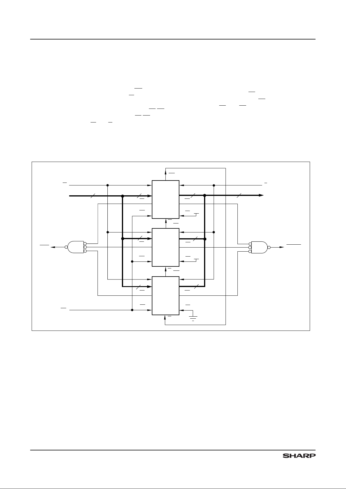
Depth Cascading
Depth cascading is implemented by configuring the
required nu mber of LH540205s in dept h-casca ded mode.
In this arrangem ent, the FIFOs are c onnected in a circular
fashion, with the Expansion Out output (XO) of each
device tied to the Expansion In input (XI) of the next
device. One FIFO in the c ascad e must be designat ed as
the ‘f irst - load’ device, by t ying its First Load in put ( FL/RT)
to ground. Al l ot her devices must have th e ir FL/RT inpu ts
tied HIGH. In this mode, W and R signals are shared by
all devices, while logic within each LH540205 controls the
steering of data. Only one LH540205 is enabled during
any given write cycle; thus, the common Data In inputs of
all devices are tied together. Likewise, only one
LH540205 is enabled during any given read cycle; thus,
the common Da ta Out outputs of all devices are wireORed toget her
In depth-cascaded mode, external logic should be
used t o gene rate a composite F u ll Flag and a compos ite
Empty Flag, by ANDing the FF ou tputs of all LH540205
devices together and ANDing the EF outputs of all devices
together. Since FF and EF are assertive-LOW signals,
this ‘ANDing’ actually is implemented using an assert iveHIGH physical OR gate. The Half-Full Flag and the
Retransmit function are not available in depth-cascaded m ode.
LH540205
RS
RS
FF
9
9
RS
W
FF
RS
FF
9
9
9
R
9
FL
FL
EF
XI
XO
FL
EF
Vcc
Vcc
XO
XO
9
9
XI
540205-19
XI
EMPTY
FULL
EF
LH540205
LH540205
DATA IN
D
0
- D
8
DATA OUT
Q
0
- Q
8
Figur e 5. FIFO Depth Cascading ( 24576 × 9)
LH540205 CMOS 8192 × 9 Asynchronous FIFO
6
 Loading...