


Sharp LH53B16R00N Datasheet
LH53B16R00
CMOS 16M (1M × 16/51 2K × 32) MROM
FEATURES
•• 1,048,5 76 × 16 bit organization
(Word mode: W = VIL)
524,288 × 32 bit organization
(Double Word mode: W = VIH)
•• Access time: 120 ns (MAX.)
Access time in page mode : 50 ns (MAX.)
•• Supply curre nt :
– Operating: 180 mA (MAX.)
– Standby: 300 µA (MAX.)
•• TTL compatible I/O
•• Three-state outputs
•• Singl e +5 V p owe r su ppl y
•• Static operation
•• Packa ge:
70-pi n , 500 -mil SSOP
•• Others:
– Non prog rammab le
– Not de sign ed o r ra ted a s rad iation
– harden ed
– CMOS process (P typ e sil icon
substrate)
DESCRIPTION
The LH53B16R00 is a 16M-bit CMOS mask ROM
(mask-programmable-read-only mem ory) organized as
1,048,576 × 16 bits (Word mode) or 524,288 × 32 bits
(Double Word mode). It is fabricated using silicon-gate
CMOS process technology.
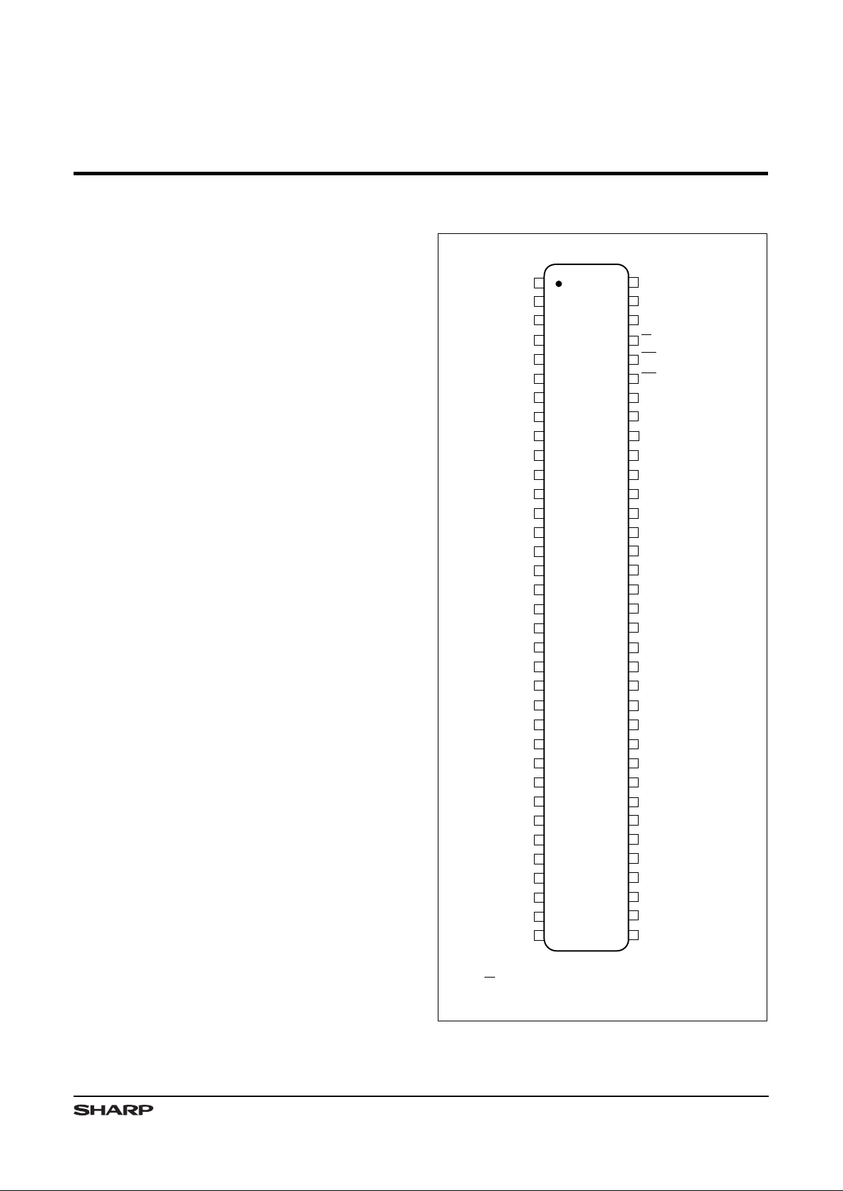
PIN CONNECTIONS
53B16R00-1
TOP VIEW
2
3
4
5
8
9
D
0
A
4
67
66
65
64
63
62
59
56
A
2
A
3
6
7V
CC
V
CC
A
5
61
60
W
OE
GND
D
15
D
13
10
11
12
69
68 NC
D
16
13 58
D
29
V
CC
GND
57
GND
D
1
CE
70-PIN SSOP
14
15
16
17
18
19
20
21
53
50
55
54
52
51
D
12
D
27
D
11
D
26
D
20
D
5
D
4
D
3
D
18
D
19
D
2
D
21
GND GND
D
31/A-1
(NOTE)
D
30
D
28
NC701
A
1
A
0
22 49
D
10
D
17
D
14
NC
46
43
48
47
V
CC
23
24
25
26 45
D
8
D
24
D
9
44
V
CC
27
28
29
30
31
32
33
34
40
37
42
41
39
38
A
18
A
17
A
16
A
15
A
9
A
10
A
8
A
6
A
7
GND
A
11
A
12
V
CC
NC
35 36
A
14
A
13
D
6
D
7
D
23
D
22
D
25
NOTE: D31/A-1 pin becomes LSB address input (A-1) when the
W pin is set to be LOW in word mode, and data output
(D
31
) when set to be HIGH in double word mode.
Figure 1. Pin Connecti ons
1
53B16R00-2
A
3
A
2
A
12
A
11
A
10
A
9
A
8
35
34
33
32
29
4
3
A
7
A
6
A
4
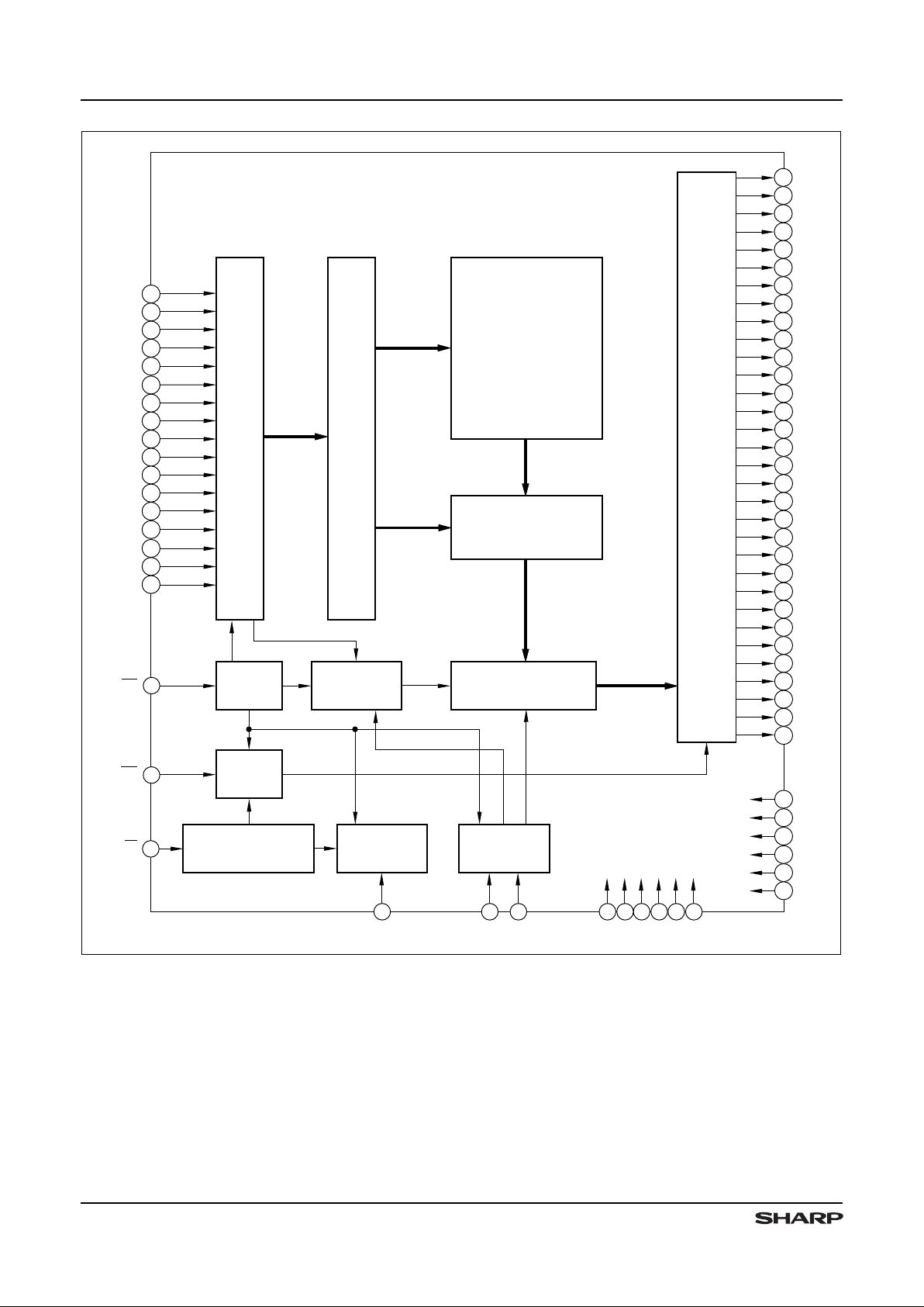
MEMORY
MATRIX
(1,048,576 x 16)
(524,288 x 32)
SENSE AMPLIFIER
30
67
5
31
A
5
6
A
13
36
ADDRESS BUFFER
CE
ADDRESS DECODER
COLUMN SELECTOR
CE
BUFFER
OE
BUFFER
A
14
37
A
15
38
65
TIMING
GENERATOR
A
16
39
W
A
17
40
A
18
41
ADDRESS
BUFFER
WORD/DOUBLE
WORD SWITCHOVER
CIRCUIT
66
OE
ADDRESS
BUFFER
DATA SELECTOR/OUTPUT BUFFER
D
3
D
2
D
1
D
7
D
6
D
4
D
5
D
0
20
14
10
8
59
16
26
D
8
44
D
9
46
18
24
D
13
D
12
D
11
D
17
D
16
D
14
D
15
D
10
62
54
52
50
56
11
D
18
15
D
19
17
60
9
D
23
D
22
D
21
D
27
D
26
D
24
D
25
D
20
47
25
21
19
27
53
D
28
55
D
29
57
D
30
61
D
31
63
45
51
63
A
-1
A
0
1
A
1
2
V
CC
GND
48
64
49
28
22
12
5823 437 13
Figure 2. LH53B16R00 Block Diagram
LH53B16 R00 CMOS 1 6M (1 M x 16/512 K x 32) MROM
2