

Sharp LH28F160S3HT-L10A Datasheet

®
PRODUCT SPECIFICATIONS
Integrated Circuits Group
LH28F160S3HT-L10A
Flash Memory
16M (2MB × 8/1MB × 16)
(Model No.: LHF16KA7)
Spec No.: EL127111A
Issue Date: August 29, 2000
SHARP
. -
l
Handle this document carefully for it contains material protected by international copyright
law. Any reproduction, full or in part, of this material is prohibited without the express
written permission of the company.
l
When using the products covered herein, please observe the conditions written herein
and the precautions outlined in the following paragraphs. In no event shall the company
be liable for any damages resulting from failure to strictly adhere to these conditions and
precautions.
(1) The products covered herein are designed and manufactured for the following
application areas. When using the products covered herein for the equipment listed
in Paragraph (2), even for the following application areas, be sure to observe the
precautions given in Paragraph (2). Never use the products for the equipment listed
in Paragraph (3).
i *Office electronics
l
instrumentation and measuring equipment
l
Machine tools
aAudiovisual equipment
*Home appliance
l
Communication equipment other than for trunk lines
LHF16KA7
-
(2) Those contemplating using the products covered herein for the following equipment
which demands high reliability, should first contact a sales representative of the
company and then accept responsibility for incorporating into the design fail-safe
operation, redundancy, and other appropriate measures for ensuring reliability and
safety of the equipment and the overall system.
-Control and safety devices for airplanes, trains, automobiles, and other
transportation equipment
*Mainframe computers
l
Tcaff
ic control systems
aGas leak detectors and automatic cutoff devices
*Rescue and security equipment
@Other safety devices and safety equipment, etc.
(3) Do not use the products covered herein for the following equipment which demands
extremely high performance in terms of functionality, reliability, or accuracy.
aAerospace equipment
l
Communications equipment for trunk lines
l
Control equipment for the nuclear power industry
l
Medical equipment related to life support, etc.
(4) Please direct all queries and comments regarding the interpretation of the above
three Paragraphs to a sales representative of the company.
l
Please direct all queries regarding the products covered herein to a sales representative
of the company.
Rev.1.9
SHARP
. -
_-
--
LHF16KA7
CONTENTS
PAGE PAGE
1
I INTRODUCTION
1.1 Product Overview.. .............................................. 3
2 PRINCIPLES OF OPERATION
2.1
Data Protection ................................................... 7
3 BUS OPERATION.. ..................................................
3.1 Read
3.2 O&put
3.3 Standby.. ............................................................. 7
3.4 Deep Power-Down .............................................. 7
3.5 Read Identifier Codes Operation.. ....................... 8
3.6 Query Operation
3.7 Write.. .................................................................. 8
1 COMMAND
4.1 Read Array Command
4.2 Read Identifier Codes Command ...................... 11
4.3 Read Status Register Command.. ..................... 11
4.4 Clear Status Register Command.. .....................
4.5 Query Command
4.51 Block Status Register
4.5.2 CFI Query Identification StAng.. ................... 13
4.5.3 System Interface.lnformation..
4.5.4 Device Geometry
4.5.5 SCS OEM Specific Extended Query Table.. 14
4.6 Block Erase Command.. ....................................
4.7 Full Chip Erase Command
4.8 Word/Byte Write Command.. ............................. 16
4.9 Multi Word/Byte Write Command ...................... 16
4.10 Block Erase Suspend Command.. ................... 17
4.11 (Multi) Word/Byte Write Suspend Command ... 17
4.12 Set Block Lock-Bit Command.. ........................ 18
4.13 Clear Block Lock-Bits Command..
4.14 STS Configuration Command
................................................................... 7
...................................................... 3
................................ 6
Disable
....................................................
.................................................. 8
DEFINITIONS.. ..................................... 8
....................................... 11
............................................... 12
.................................. 12
.....................
Definition ......................... 14
................................ 15
...................
.........................
5 DESIGN CONSIDERATIONS
5.1 Three-Line Output Control
5.2 STS and Block Erase, Full Chip Erase, (Multi)
Word/Byte Write and Block Lock-Bit Configuration
Polling ................................................................ 3c
5.3 Power Supply Decoupling .................................. 3c
5.4 V,, Trace on Printed Circuit Boards..
7
5.5 Vcc,
5.6 Power-Up/Down Protection..
7
5.7 Power Dissipation
6 ELECTRICAL SPECIFICATIONS..
6.1 Absolute Maximum Ratings
6.2 Operating Conditions ......................................... 32
6.2.1 Capacitance ................................................. 32
6.2.2 AC Input/Output Test Conditions..
6.2.3 DC Characteristics ........................................ 34
6.2.4 AC Characteristics - Read-Only Operations .3E
6.2.5 AC Characteristics - Write Operations..
11
13
15
18
19
6.2.6 Alternative CE#-Controlled Writes..
6.2.7 Reset Operations
6.2.8 Block Erase, Full Chip Erase, (Multi)
7 ADDITIONAL INFORMATION ................................ 4E
7.1 Ordering Information .......................................... 46
V,,,, RP# Transitions.. .............................. .31
............................................. .31
Word/Byte Write and Block Lock-Bit
Configuration Performance..
................................
................................ .3C
.............................
........................
.............................. .3i
........................................ .4Z
........................
...............
...............
....... .3E
.............
.3C
.3C
.31
.3i
.3Z
.41
.44
Rev. 1.9
SHAl?P
LHFlGKA7 2
-
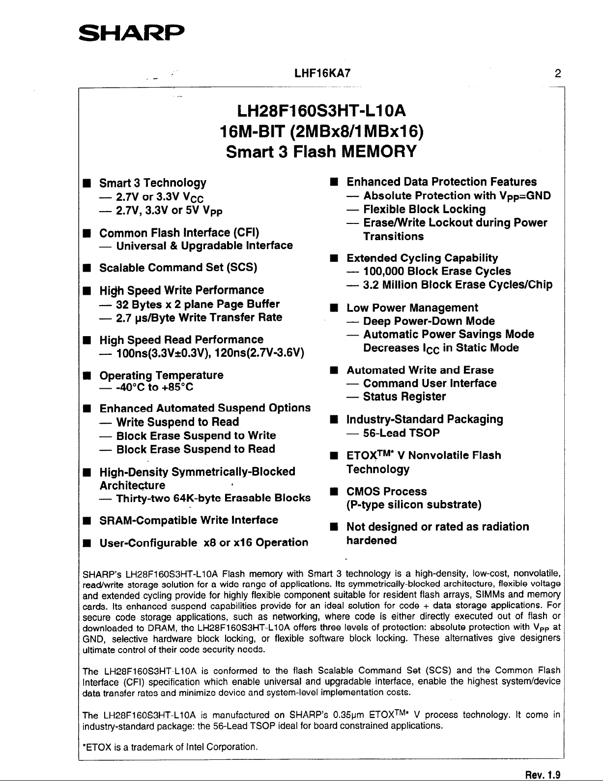
LH28F160S3HT-Ll OA
1 GM-BIT (2MBx8/1 MBxl6)
Smart 3 Flash MEMORY
n Smart 3 Technology
- 2.7V or 3.3V Vcc
- 2.7V, 3.3V or SV Vpp
I Common Flash Interface (CFI)
-
Universal & Upgradable Interface
I Scalable Command Set (SCS)
n High Speed Write Performance
-
32 Bytes x 2 plane Page Buffer
-
2.7 @Byte Write Transfer Rate
n High Speed Read Performance
- 1 OOns(3.3V*O.3V), 120ns(2.7\1-3.6V)
I Operating Temperature
- -40°C to +85X
n Enhanced Automated Suspend Options
-
Write Suspend to Read
- Block Erase Suspend to Write
-
Block Erase Suspend to Read
n High-Density Symmetrically-Blocked
Architecture
-
Thirty-two 64K-byte Erasable Blocks
n Enhanced Data Protection Features
- Absolute Protection with VpP=GND
- Flexible Block Locking
- Erase/Write Lockout during Power
Transitions
n Extended Cycling Capability
- 100,000 Block Erase Cycles
- 3.2 Million Block Erase Cycles/Chip
n Low Power Management
- Deep Power-Down Mode
- Automatic Power Savings Mode
Decreases ICC in Static Mode
n Automated Write and Erase
- Command User Interface
- Status Register
n Industry-Standard Packaging
- 56-Lead TSOP
n ETOgTM* V Nonvolatile Flash
Technology
n CMOS Process
(P-type silicon substrate)
I SRAM-Compatible Write Interface
I User-Configurable x8 or x16 Operation
SHARP’s LH28F160S3HT-LlOA Flash memory with Smart 3 technology is a high-density, low-cost, nonvolatile,
*cad/write storage solution for a wide range of applications. Its symmetrically-blocked architecture, flexible voltage
and extended cycling provide for highly flexible component suitable for resident flash arrays, SlMMs and memory
:ards. Its enhanced suspend capabilities provide for an ideal solution for code + data storage applications. For
secure code storage applications, such as networking, where code is either directly executed out of flash or
downloaded to DRAM, the LH28F160S3HT-LlOA offers three levels of protection: absolute protection with V,, at
?ND, selective hardware block locking, or flexible software block locking. These alternatives give designers
Jltimate control of their code security needs.
The LH28F160S3HT-LlOA is conformed to the flash Scalable Command Set (SCS) and the Common Flash
nterface (CFI) specification which enable universal and upgradable interface, enable the highest system/device
data transfer rates and minimize device and system-level implementation costs.
The LH28F160S3HT-LlOA is manufactured on SHARP’s 0.35um
ndustry-standard package: the 56-Lead TSOP ideal for board constrained applications.
‘ETOX is a trademark of Intel Corporation.
n Not designed or rated as radiation
hardened
ETOX TM* V process technology. It come in
Rev. 1.9
SHARP
. -
LHFlGKA7
1 INTRODUCTION
This datasheet contains LH28F160S3HT-Ll OA
specifications. Section 1 provides a flash memory
overview. Sections 2, 3, 4, and 5 describe the
memory organization and functionality. Section 6
covers electrical specifications.
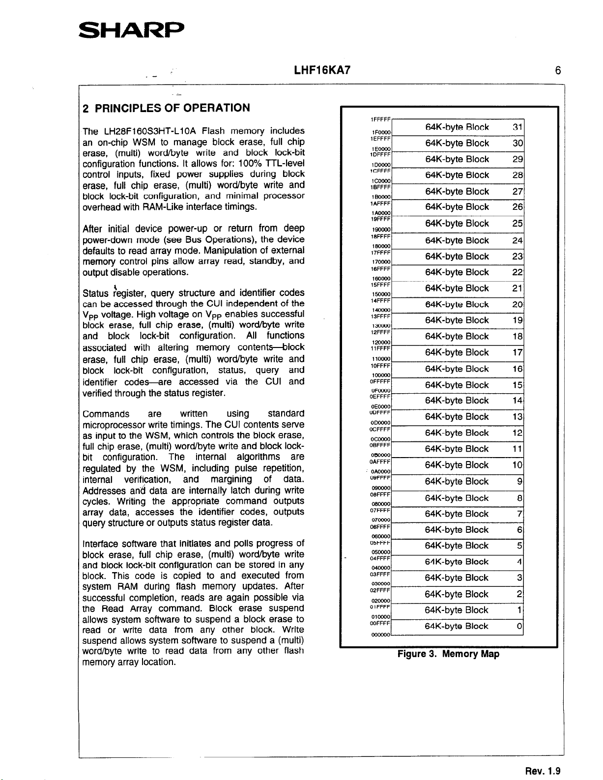
1 .l Product Overview
The LH28F160S3HT-Ll OA is a high-performance
16M-bit Smart 3 Flash memory organized as
2MBx80MBxl6. The 2MB of data is arranged in
thirty-two 64K-byte blocks which are individually
erasable, lockable, and unlockable in-system. The
memory map is shown in Figure 3.
Smart 3’ technology provides a choice of V,, and
V,, combinations, as shown in Table 1, to meet
system performance and power expectations. 2.7V
Vc, consumes approximately one-fifth the power of
5V Vc,. V,, at 2.7V, 3.3V and 5V eliminates the
need for a separate 12V converter, while V,,=5V
maximizes erase and write performance. In addition
to flexible erase and program voltages, the dedicated
V,, pin gives complete data protection when
Table 1. Vcc and Vpp Voltage Combinations
Offered by Smart 3 Technology
Vcc Voltage Vpp Voltage
2.7V 2.7V, 3.3V, 5V
3.3v 3.3v, 5v
Internal
automatically configures the device for optimized
read and write operations.
VW
and
VP,
detection Circuitry
3
1
write suspend mode enables the system to read data
or execute code from any other flash memory array
location.
Individual block locking uses a combination of bits
and WP#, Thirty-two block lock-bits, to lock ant
unlock blocks. Block lock-bits gate block erase, full
chip erase and (multi) word/byte write operations.
Block lock-bit configuration operations (Set Block
Lock-Bit and Clear Block Lock-Bits commands) sei
and cleared block lock-bits.
The status register indicates when the WSM’s block
erase, full chip erase, (multi) word/byte write or block
lock-bit configuration operation is finished.
The STS output gives an additional indicator of WSM
activity by providing both a hardware signal of status
(versus software polling) and status maskins
(interrupt masking for background block erase, fol
example). Status polling using STS minimizes bott
CPU overhead and system power consumption. STS
pin can be configured to different states using the
Configuration command. The STS pin defaults tc
RY/BY# operation. When low, STS indicates that the
WSM is performing a block erase, full chip erase
(multi) word/byte write or block lock-bit configuration
STS-High Z indicates that the WSM is ready for a
new command, block erase is suspended and (multi:
word/byte write are inactive, (multi) word/byte write
are suspended, or the device is in deep power-dowr
mode. The other 3 alternate configurations are al
pulse mode for use as a system interrupt.
The access time is 100ns (tAVQv) over the extendec
temperature range (-40°C to +85”C) and Vc, suppI\
voltage range of 3.OV-3.6V. At lower V,, voltage, the
access time is 120ns (2.7V-3.6V).
A Command User Interface (CUI) serves as the
interface between the system processor and internal
operation of the device. A valid command sequence
written to the CUI initiates device automation. An
internal Write State Machine (WSM) automatically
executes the algorithms and timings necessary for
block erase, full chip erase, (multi) word/byte write
and block lock-bit configuration operations.
4 block erase operation erases one of the device’s
%lK-byte blocks typically within 0.41s (3.3V Vcc, 5V
VP,) independent of other blocks. Each block can be
independently erased 100,000 times (3.2 million
olock erases per device). Block erase suspend mode
allows system software to suspend block erase to
read or write data from any other block.
A word/byte write is performed in byte increments
typically within 12.95ps (3.3V V,,, 5V VP,). A multi
word/byte write has high speed write performance of
2.7@byte (3.3V V,,, 5V VP,). (Multi) Word/byte
The Automatic Power Savings (APS) feature
substantially reduces active current when the device
is in static mode (addresses not switching). In APS
m‘ode, the typical I,,, current is 3 mA at 3.3V V,c.
When either CE,# or CE,#, and RP# pins are at V,,
the I,, CMOS standby mode is enabled. When the
RP# pin is at GND, deep power-down mode ic
enabled which minimizes power consumption and
provides write protection during reset. A reset time
(tPHav) is required from RP# switching high until
outputs are valid. Likewise, the device has a wake
time (tPHEL) from RP#-high until writes to the CUI are
recognized. With RP# at GND, the WSM is reset and
the status register is cleared.
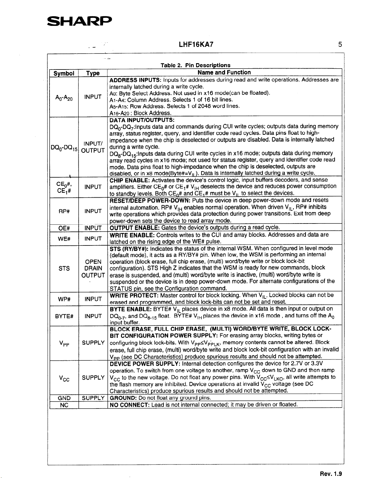
The device is available in 56-Lead TSOP (Thin Small
Outline Package, 1.2 mm thick). Pinout is shown in
Figure 2.
Rev. 1.9
SHARP
LHFlGKA7 4
Comparator
I/ + b
Cl3
WEX
OE%
RP#
WP#
II-4 I
kE,#
./
VCC
CEo#
VPP
RP#
GND
NC
NC
Azo
AIS
Al6
A17
Al6
A15
Al.4
A13
Al2
41
AIO
As
Ae
A7
As
A5
2
A2
AI
:
3
4
5
6
‘7
8
9
10
11
12
13
14
15
16
17
18
19
20
21
22
d 23
24
25
26
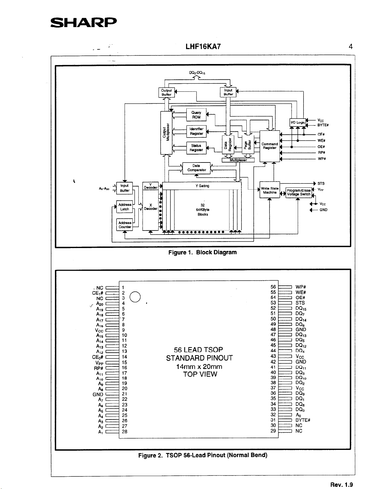
Figure 1. Block Diagram
56 LEAD TSOP
STANDARD PINOUT
14mm x 20mm
TOP VIEW
----G-L
53
52
51
50
49
48
47
46
45
44
43
42
41
40
39
38
37
36
35
34 1
33 I
32 I
31 )
30
29
WP#
WE#
OE#
STS
DQ15
z:,
DQ6
GND
DQ13
DQ5
DQ12
DQ4
vcc
GND
DQll
DQ3
DQlo
DQz
vcc
DQP
DQ;
DQe
DQo
A0
BYTE#
NC
NC
Figure 2. TSOP 56-Lead Pinout (Normal Bend)
Rev. 1.9
SHARP
*o-*20
x&)-DC+!
CEO%
CE,#
RP#
OE#
WE#
STS
WP#
BYTE#
“PP
“cc
GND
NC
I
_ -
Type
INPUT
INPUT/
3UTPUT
INPUT
INPUT
INPUT
INPUT
OPEN
DRAIN
OUTPUT
tWPUT
lNPUT
SUPPLY
SUPPLY
SUPPLY
LHF16KA7
-
Table 2. Pin Descriptions
T
ADDRESS INPUTS: Inputs for addresses during read and write operations. Addresses are
internally latched during a write cycle.
Ao: Byte Select Address. Not used in x16 mode(can be floated).
AI-AK Column Address. Selects 1 of 16 bit lines.
A+Ai5: Row Address. Selects 1 of 2048 word lines.
A164420
DATA INPUT/OUTPUTS:
DQo-DQ,:lnputs data and commands during CUI write cycles; outputs data during memory
array, status register, query, and identifier code read cycles. Data pins float to highimpedance when the chip is deselected or outputs are disabled. Data is internally latched
during a write cycle.
DQs-DQ15:lnpUtS data during CUI write cycles in x16 mode; outputs data during memory
array read cycles in xl 6 mode; not used for status register, query and identifier code read
mode. Data pins float to high-impedance when the chip is deselected, outputs are
disabled, or in x8 mode(Byte#=V,, ). Data is internally latched during a write cycle.
CHIP ENABLE: Activates the device’s control logic, input buffers decoders, and sense
amplifiers. Either CE,# or CE,# V,, deselects the device and reduces power consumption
to standby levels. Both CE,-# and CE,# must be V,, to select the devices.
RESET/DEEP POWER-DOWN: Puts the device in deep power-down mode and resets
internal automation. RP# V,, enables normal operation. When driven \JIL, RP# inhibits
write operations which provides data protection during power transitions. Exit from deep
power-down sets the device to read array mode.
OUTPUT ENABLE: Gates the device’s outputs during a read cycle.
WRITE ENABLE: Controls writes to the CUI and array blocks. Addresses and data are
latched on the rising edge of the WE# pulse.
STS (RY/BY#): Indicates the status of the internal WSM. When configured in level mode
(default mode), it acts as a RY/BY# pin. When low, the WSM is performing an internal
operation (block erase, full chip erase, (multi) word/byte write or block lock-bit
configuration). STS High Z indicates that the WSM is ready for new commands, block
erase is suspended, and (multi) word/byte write is inactive, (multi) word/byte write is
suspended or the device is in deep power-down mode. For alternate configurations of the
STATUS pin, see the Configuration command.
WRITE PROTECT: Master control for block locking. When V,,, Locked blocks can not be
erased and programmed, and block lock-bits can not be set and reset.
BYTE ENABLE: BYTE# V,, places device in x8 mode. All data is then input or output on
DQO-,, and DQse15 float. BYTE# V,, places the device in x16 mode , and turns off the A,
input buffer.
BLOCK ERASE, FULL CHIP ERASE, (MULTI) WORD/BYTE WRITE, BLOCK LOCK-
BIT CONFIGURATION POWER SUPPLY: For erasing array blocks, writing bytes or
configuring block lock-bits. With V+V+~,K, memory contents cannot be altered. Block
erase, full chip erase, (multi) word/byte write and block lock-bit configuration with an invalid
vpp (see DC Characteristics) produce spurious results and should not be attempted.
DEVICE POWER SUPPLY: Internal detection configures the device for 2.7” or 3.3”
operation. To switch from one voltage to another, ramp V,, down to GND and then ramp
V,, to the new voltage. Do not float any power pins. With V,,IV,,,, all write attempts to
the flash memory are inhibited. Device operations at invalid V,, voltage (see DC
Characteristics) produce spurious results and should not be attempted.
GROUND: Do not float any ground pins.
NO CONNECT: Lead is not internal connected; it may be driven or floated.
: Block Address.
Name and Function
5
I
I
Rev. 1.9
SHARP
. -
r
.i
2 PRINCIPLES OF OPERATION
The LH28F160S3HT-Ll OA Flash memory includes
an on-chip WSM to manage block erase, full chip
erase, (multi) word/byte write and block lock-bit
configuration functions. It allows for: 100% TTL-level
control inputs, fixed power supplies during block
erase, full chip erase, (multi) word/byte write and
block lock-bit configuration, and minimal processor
overhead with RAM-Like interface timings.
After initial device power-up or return from deep
power-down mode (see Bus Operations), the device
defaults to read array mode. Manipulation of external
memory control pins allow array read, standby, and
output disable operations.
Status :egister, query structure and identifier codes
can be accessed through the CUI independent of the
V,, voltage. High voltage on VPP enables successful
block erase, full chip erase, (multi) word/byte write
and block lock-bit configuration. All functions
associated with altering memory contents-block
erase, full chip erase, (multi) word/byte write and
block lock-bit configuration, status, query and
identifier codes-are accessed via the CUI and
verified through the status register.
Commands are
microprocessor write timings. The CUI contents serve
as input to the WSM, which controls the block erase,
full chip erase, (multi) word/byte write and block lockbit configuration. The internal algorithms are
regulated by the WSM, including pulse repetition,
internal verification,
Addresses and data are internally latch during write
cycles. Writing the appropriate command outputs
array data, accesses the identifier codes, outputs
query structure or outputs status register data.
Interface software that initiates and polls progress of
block erase, full chip erase, (multi) word/byte write
and block lock-bit configuration can be stored in any
block. This code is copied to and executed from
system RAM during flash memory updates. After
successful completion, reads are again possible via
the Read Array command. Block erase suspend
allows system software to suspend a block erase to
read or write data from any other block. Write
suspend allows system software to suspend a (multi)
word/byte write to read data from any other flash
memory array location.
written using standard
and margining of data.
LHFlGKA7 6
64K-byte Block
1AFFFF
1 AOOW
ISFFFF
1SOOCKl
1SFFFF
laOW0
17FFFF
17OmO
IGFFFF
160000
15FFFF
15OoM)
14FFFF
14oooo
13FFFF
,-mm
IPFFFF
4~cyyI
1lFFFF
11ocw
1OFFFF
lcmoa
OFFFFF
OFOOOO
OEFFFF
OEOOOO
OIJFFFF
ODoooO
OCFFFF
ocoooo
OBFFFF
OAFFFF
OAOWO
OSFFFF
OSOWO
08FFFF
OKCOO
07FFFF
07wOo
OGFFFF
060000
OBFFFF
nE-n
04FFFF
04OWO
OIFFFF
03Ocm
OZFFFF
OZWOO
01 FFFF
01wo0
OOFFFF
64K-byte Block 26
64K-byte Block 25
64K-byte Block 24
64K-byte Block 23
64K-byte Block 22
64K-byte Block 21
64K-byte Block 20
64K-byte Block 19
64K-byte Block
64K-byte Block 17
64K-byte Block 16
64K-byte Block 15
64K-byte Block 14
64K-byte Block 13
64K-byte Block 12
64K-byte Block 11
64K-byte Block 10
64K-byte Block 9
64K-byte Block 8
64K-byte Block 7
64K-byte Block 6
64K-byte Block 5
64K-byte Block 4
64K-byte Block
64K-bvte Block 0
Figure 3. Memory Map
3’1
‘81
3 64K-byte Block
2 64K-byte Block
1
1
L
Rev. 1.9
SHARP
LHFlGKA7
-
2.1 Data Protection
Depending on the application, the system designer
may choose to make the V,, power supply
switchable (available only when block erase, full chip
erase, (multi) word/byte write and block lock-bit
configuration are required) or hardwired to VPPH1,2/3.
The device accommodates either design practice and
encourages optimization of the processor-memory
interface.
When Vpp~VppLKt
altered. The CUI, with multi-step block erase, full chip
erase, (multi) word/byte write and block lock-bit
configuration command sequences, provides
protection from unwanted operations even when high
voltage,is applied to V,,. All write functions are
disabled when Vcc is below the write lockout voltage
V,,, or when RP# is at V,,. The device’s block
locking capability provides additional protection from
inadvertent code or data alteration by gating block
erase, full chip erase and (multi) word/byte write
operations.
memory contents cannot be
3 BUS OPERATION
The local CPU reads and writes flash memory insystem. All bus cycles to or from the flash memory
conform to standard microprocessor bus cycles.
3.1 Read
Information can be read from any block, identifier
codes, query structure,‘or status register independent
of the V,, voltage. RP# must be at VI,.
The first task is to write the appropriate read mode
command (Read Array, Read Identifier Codes, Query
or Read Status Register) to the CUI. Upon initial
device power-up or after exit from deep power-down
mode, the device automatically resets to read array
mode. Five control pins dictate the data flow in and
out of the component: CE# (CE,#, CE,#), OE#, WE#,
RP# and WP#. CE,#, CE,# and OE# must be driven
active to obtain data at the outputs. CE,#, CE,# is
the device selection control, and when active enables
the selected memory device. OE# is the data output
(DC&-DQ,,) control and when active drives the
selected memory data onto the I/O bus. WE# and
RP# must be at V,,. Figure 17, 18 illustrates a read
cycle.
7
3.2 Output Disable
With OE# at a logic-high level (VI,), the devict
outputs are disabled. Output pins DO,-DQ,, an
placed in a high-impedance state.
3.3 Standby
Either CE,# or CE,# at a logic-high level (V,,) place:
the device in standby mode which substantiall!
reduces device power consumption. DQo-DQ,,
outputs are placed in a high-impedance statt
independent of OE#. If deselected during bloc1
erase, full chip erase, (multi) word/byte write ant
block lock-bit configuration, the device continue:
functioning, and consuming active power until the
operation completes.
3.4 Deep Power-Down
RP# at V,, initiates the deep power-down mode.
In read modes, RP#-low deselects the memory
places output drivers in a high-impedance state ant
turns off all internal circuits. RP# must be held low fol
a minimum of 100 ns. Time t,,crv is required after
return from power-down until initial memory access
outputs are valid. After this wakeup interval, norma
operation is restored. The CUI is reset to read arra)
mode and status register is set to 80H.
During block erase, full chip erase, (multi) word/byte
write or block lock-bit configuration modes, RP#-low
will abort the operation. STS remains low until the
reset operation is complete. Memory contents being
altered are no longer valid; the data may be partially
erased or written. Time tPHWL is required after RP#
goes to logic-high (V,,) before another command can
be written.
As with any automated device, it is important tc
assert RP# during system reset. When the system
comes out of reset, it expects to read from the flash
memory. Automated flash memories provide status
information when accessed during block erase, full
chip erase, (multi) word/byte write and block lock-bit
configuration. If a CPU reset occurs with no flash
memory reset, proper CPU initialization may not
occur because the flash memory may be providing
status information instead of array data. SHARP’s
flash memories allow proper CPU initialization
following a system reset through the use of the RP#
input. In this application, RP# is controlled by the
same RESET# signal that resets the system CPU.
-l
Rev. 1 .Q
_ -
I
--
LHFlGKA7
8
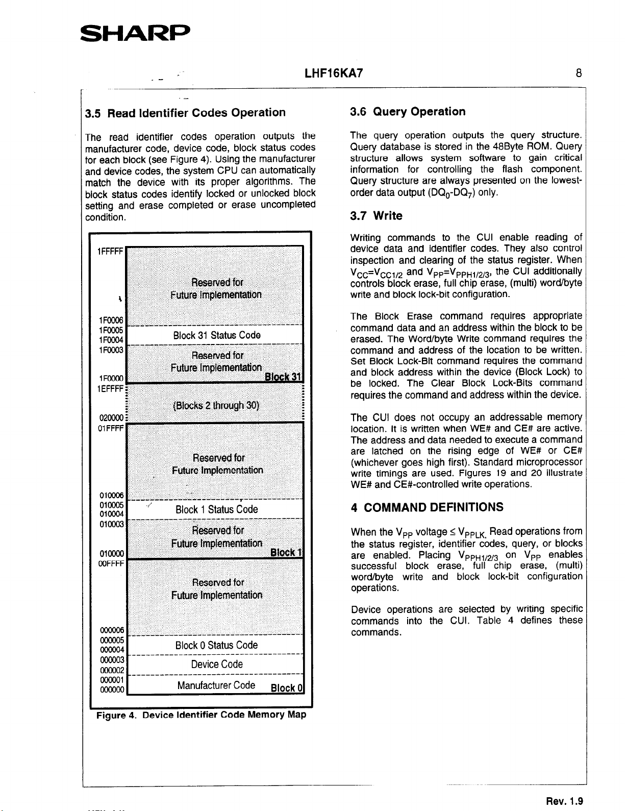
3.5 Read Identifier Codes Operation
The read identifier codes operation outputs the
manufacturer code, device code, block status codes
for each block (see Figure 4). Using the manufacturer
and device codes, the system CPU can automatically
match the device with its proper algorithms. The
block status codes identify locked or unlocked block
setting and erase completed or erase uncompleted
condition.
1FFFFF :.. :
l !", ,: :.
,Fm; .. :.
,K)oo5
IF0004
,Fooo3 T ---,-. ~ _____ --; ____ T-------y---I
,Foooo :,. ., :‘i:
IEFFFF;:. :' . ; : ':,,..
02oooo; ,+ ..: ,, '. ', : .,. :.
OlFFFF ',
o,o(y& (I ” y.,
01ooo5 ./’
010004
010003-
01~ 1. .,: .’ ‘.,
OOFFFF ;. 1.
ooooO6 . .
coo005
OoOcQ4
OOanI3
OOmO2
oooQo1
'.
: :. . . .,.
>
. . . .
..A. 1;; ,, . . .
,., . .
:'.. ;.
;.
iilr-' l_l..d+ - -----------_-------1----
.: ,;.'
'. .' j.: R&&&&, .,:, ': .:' .:
.. Future ~+irnentatt~n '.
Block 31 Status Code
JGxwv~d for
;.
:.
m..
w.
:.
tfutye h$e.merrtiian
: :
: . . '(~ioiks2thi~gl-l~) ;
" : ..,I. ; ,:" "')
: B&;k31
l---l-l---l-~--l’l-l----rll---lll-l---------
___________ --- ______ ---__----------
: .;
Block 1 Status Code
. . ..
i&e&ed~for ,:
:.. .: .f;uture:‘tmplemen~tiQn ..
Block”
Resewed far
Future Implementation
___- -- ____ -- ____ --------_------ -----_____-_____-_______-----------------____________________-----------------
Block 0 Status Code
Device Code
Manufacturer Code
Block (
3.6 Query Operation
The query operation outputs the query structure.
Query database is stored in the 48Byte ROM. Query
structure
information for controlling the flash component.
Query structure are always presented on the lowest-
order data output (DQc-DQ,) only.
allows system software to gain critical
3.7 Write
Writing commands to the CUI enable reading of
device data and identifier codes. They also control
inspection and clearing of the status register. When
Vcc=Vcc1,2 and VPP=VPPHt/2/3, the CUI additionally
controls block erase, full chip erase, (multi) wordlbyte
write and block lock-bit configuration.
The Block Erase command requires appropriate
command data and an address within the block to be
erased. The Word/byte Write command requires the
command and address of the location to be written.
Set Block Lock-Bit command requires the command
and block address within the device (Block Lock) to
be locked. The Clear Block Lock-Bits command
requires the command and address within the device.
The CUI does not occupy an addressable memory
location. It is written when WE# and CE# are active.
The address and data needed to execute a command
are latched on the rising edge of WE# or CE#
(whichever goes high first). Standard microprocessor
write timings are used. Figures 19 and 20 illustrate
WE# and CE#-controlled write operations.
4 COMMAND DEFINITIONS
When the V,, voltage I V,,,,, Read operations from
the status register, identifier codes, query, or blocks
are enabled. Placing V,,,,,us on V,, enables
successful block erase, full chip erase, (multi)
word/byte write and block lock-bit configuration
operations.
Device operations are selected by writing specific
commands into the CUI. Table 4 defines these
commands.
Figure 4. Device Identifier Code Memory Map
Rev. 1.9
SHARP
_- =
LHFlGKA7 9
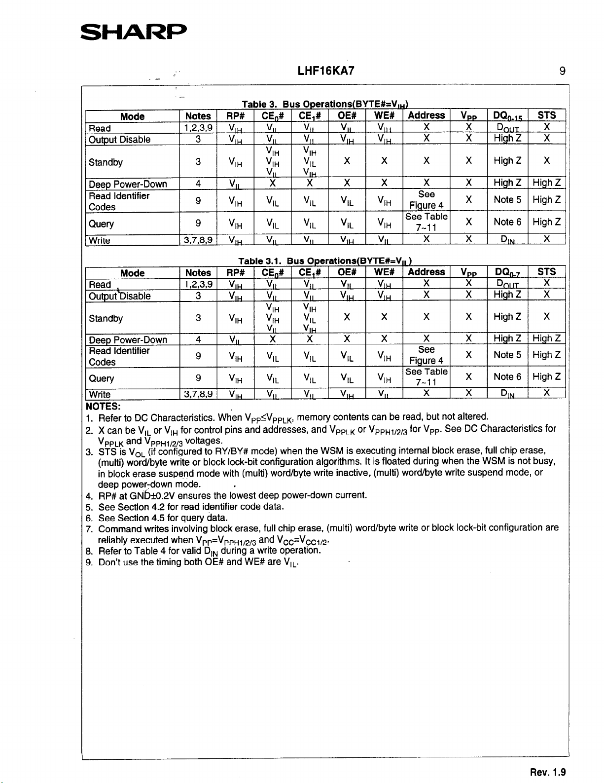
Table 3. Bus Operations(BYTE#=V,Uj
Mode
Read
Output Disable
jeep Power-Down
lead Identifier
Lodes
Query
Write
Deep Power-Down
Read Identifier
Codes
Query
Write
Notes RP#
1,2,3,9 v,w
3 V,H
CE”# CE,# OE# WE#
V,, V,, V,, V,H X X D&r X
V,,
v,,, 11 1
V,, V,w V,H X X High Z X
v
4 V,, X X X X
9
9
I
1
3,7&W
VI, %L
vlH VI, 4, VI,
I I I I I
1 ‘.‘,H 1 VII 1 VII 1 VI’I 1 VII I
VI,
%L 4, 4,
V,w
4 VI, X X X
9
9
‘1, VlL
‘1,
3,7,8,9 VI,,
VI,
VII
VI, YL ‘1,
VI,
VII
VI, vlH
V,H VII
1 Address 1 Vpp 1 DQnm15 1 STS
X X High Z High Z
See Table x
vlH
See
Figure 4
7-11
X
X Note 5 High Z
Note 6 High Z
1 x 1 DIN I x
X X X High Z High Z
See
Figure 4
SeeTable x
7-11
X Note 5 High Z
Note 6 High Z
X X DIN X
NOTES:
1. Refer to DC Characteristics. When V&f,,,,,
memory contents can be read, but not altered.
2. X can be V,, or VrH for control pins and addresses, and VP,,, or VPr+rt/2/s for V,,. See DC Characteristics for
bPLK and VPPH1/~3 voitagese
3. STS is V,, (if configured to RY/BY# mode) when the WSM is executing internal block erase, full chip erase,
(multi) word/byte write or block lock-bit configuration algorithms. It is floated during when the WSM is not busy,
in block erase suspend mode with (multi) word/byte write inactive, (multi) word/byte write suspend mode, or
deep power;down mode.
.
4. RP# at GN&O.2V ensures the lowest deep power-down current.
5. See Section 4.2 for read identifier code data.
6. See Section 4.5 for query data.
7. Command writes involving block erase, full chip erase, (multi) word/byte write or block lock-bit configuration are
reliably executed when
Vpp=VPPH1/2/3
and Vcc=Vcc1~2.
8. Refer to Table 4 for valid D,, during a write operation.
9. Don’t use the timing both OE# and WE# are VI,.
Rev. 1.9
,
SHARP
. -
I
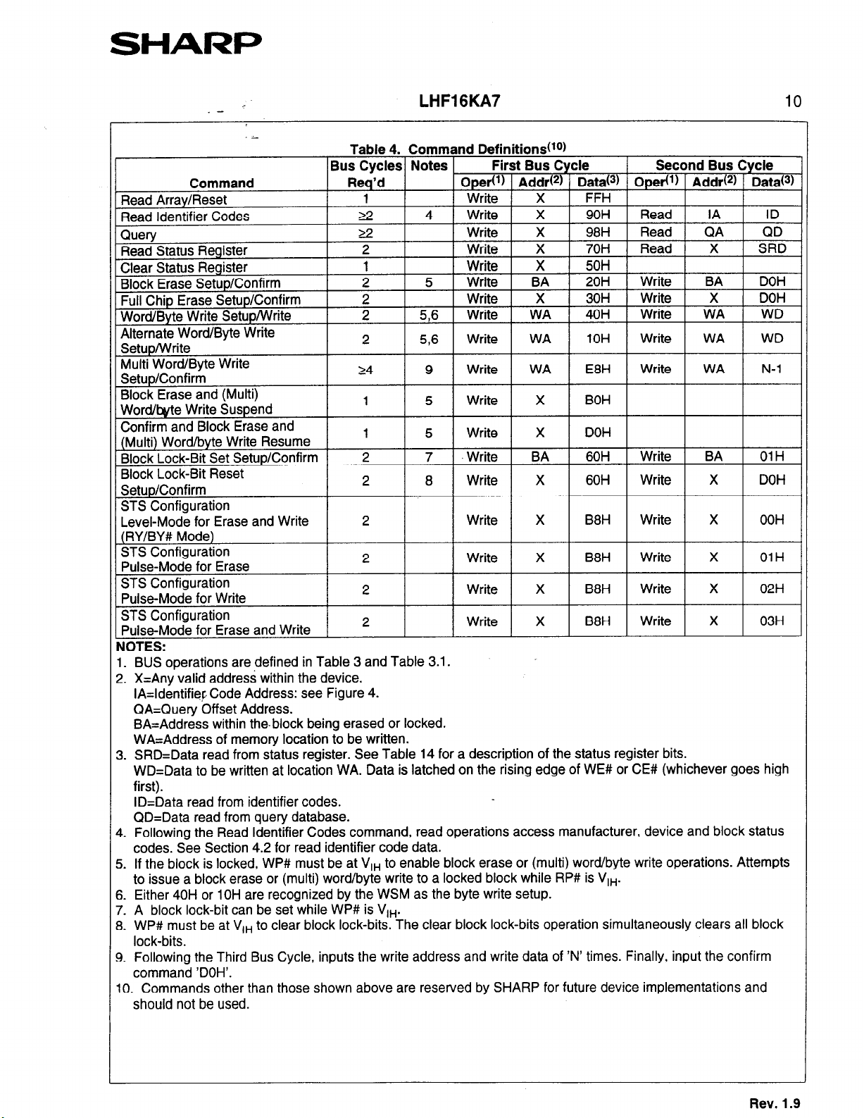
Command
Read Array/Reset
.i
Table 4. Command Definitions(l”)
Bus Cycles Notes First Bus Cycle Second Bus Cycle
Req’d
1 Write ( X 1 FFH
22 4 Write X 90H Read IA
22
2
T
2
2
2
4lternate Word/Byte Write
SetupWrite
Multi Word/Byte Write
Setup/Confirm
Block Erase and (Multi)
Word/byte Write Suspend
Confirm and Block Erase and
(Multi) Word/byte Write Resume
Block Lock-Bit Set Setup/Confirm
Block Lock-Bit Reset
Setup/Confirm
STS Configuration
Level-Mode for Erase and Write
(RY/BY# Mode)
STS Configuration
Pulse-Mode for Erase
STS Configuration
Pulse-Mode for Write
STS Configuration
Pulse-Mode for Erase and Write
NOTES:
1. BUS operations are defined in Table 3 and Table 3.1.
2. X=Any valid address within the device.
IA=ldentifiep Code Address: see Figure 4.
QA=Quety Offset Address.
BA=Address within the. block being erased or locked.
WA=Address of memory location to be written.
3. SRD=Data read from status register. See Table 14 for a description of the status register bits.
WD=Data to be written at location WA. Data is latched on the rising edge of WE# or CE# (whichever goes high
first).
ID=Data read from identifier codes.
QD=Data read from query database.
4. Following the Read Identifier Codes command, read operations access manufacturer, device and block status
codes. See Section 4.2 for read identifier code data.
5. If the block is locked, WP# must be at VI, to enable block erase or (multi) word/byte write operations. Attempts
to issue a block erase or (multi) word/byte write to a locked block while RP# is VI,.
6. Either 40H or 10H are recognized by the WSM as the byte write setup.
7. A block lock-bit can be set while WP# is VI,.
8. WP# must be at VI, to clear block lock-bits. The clear block lock-bits operation simultaneously clears all block
lock-bits.
9. Following the Third Bus Cycle, inputs the write address and write data of ‘N’ times. Finally, input the confirm
command ‘DOH’.
10. Commands other than those shown above are reserved by SHARP for future device implementations and
should not be used.
2
24
1
1 5
2
2 8 Write X
2
2
2 Write X B8H Write X 02H
2 Write X B8H
LHFlGKA7
Oper(‘)
Write X 98H Read QA C
Write X 70H Read X
Write X
5 Write BA
Write X
55
596
Write WA
Write WA 10H
9 Write WA E8H
5 Write X BOH
Write X DOH
7 Write BA 60H
Write X B8H Write X OOH
Write X B8H Write X OlH
1 Add&*) 1 Data13) Ope#) 1 Addr(*) 1 Data13)
_ . .._-
60H Write X DOH
‘D II
Write WA WD
Write WA N-l
Write BA
Write X 03H
OlH
10
I
Rev. 1.9
SHARI=
. -
--
LHF16KA7
4.1 Read Array Command 4.3 Read Status Register Command
Upon initial device power-up and after exit from deep
power-down mode, the device defaults to read array
mode. This operation is also initiated by writing the
Read Array command. The device remains enabled
for reads until another command is written. Once the
internal WSM has started a block erase, full chip
erase, (multi) word/byte write or block lock-bit
configuration, the device will not recognize the Read
Array command until the WSM completes its
operation unless the WSM is suspended via an Erase
Suspend and (Multi) Word/byte Write Suspend
command. The Read Array command functions
independently of the VP,, voltage and RP# must be
Vi,*
The
status
register may be read to determine when i
block erase, full chip erase, (multi) word/byte write OI
block lock-bit configuration is complete and whethei
the operation completed successfully(see Table 14)
It may be read at any time by writing the Read Statu:
Register command. After writing this command, al
subsequent read operations output data from the
status register until another valid command is written
The status register contents are latched on the fallins
edge of OE# or CE#(Either CE,# or CE,#)
whichever occurs. OE# or CE#(Either CE,# or CE,#:
must toggle to ‘Jr, before further reads to update the
status register latch. The Read Status Register
command functions independently of the V,, voltage
RP# must be VI,.
4.2 F&ad Identifier Codes Command
The extended status register may be read tc
The identifier code operation is initiated by writing the
Read Identifier Codes command. Following the
command write, read cycles from addresses shown in
Figure 4 retrieve the manufacturer, device, block lock
configuration and block erase status (see Table 5 for
identifier code values). To terminate the operation,
write another valid command. Like the Read Array
command, the Read Identifier Codes command
functions independently of the V,, voltage and RP#
must be V,,. Following the Read Identifier Codes
command, the following information can be read:
Table 5. Identifier Codes
Code
Manufacture Code
./
Device Code
Block Status Code
*Block is Unlocked
l Block is Locked
*Last erase operation
completed successfully
@Last erase operation did
not completed successfully
OReserved for Future Use
NOTE:
1. X selects the specific block status code to be
read. See Figure 4 for the device identifier code
memory map.
Address
00000
00001
00002
00003
x0004(’ )
x0005(‘) ~
1 / DQ,=O 1
Data
BO
DC&,=0
DQc= 1
DQ,=l
DQyw7
determine multi word/byte write availability(see Table
14.1). The extended status register may be read a
any time by writing the Multi Word/Byte Write
command. After writing this command, all subsequen
read operations output data from the extended statuz
register, until another valid command is written. Mult
Word/Byte Write command must be re-issued tc
update the extended status register latch.
4.4 Clear Status Register Command
Status register bits SR.5, SR.4, SR.3 and SR.l are
set to “1”s by the WSM and can only be reset by the
Clear Status Register command. These bits indicate
various failure conditions (see Table 14). By allowins
system software to reset these bits, severa
operations (such as cumulatively erasing or lockinc
multiple blocks or writing several bytes in sequence:
may be performed. The status register may be pollee
to determine if an error occurs during the sequence.
To clear the status register, the Clear Status Register
command (50H) is written. It functions independently
of the applied V,, Voltage. RP# must be VI,. This
command is not functional during block erase, ful
chip erase, (multi) word/byte write block lock-bii
configuration, block erase suspend or (multi:
word/byte write suspend modes.
11
Rev. 1.9
SHARP
. -
--
LHFlGKA7
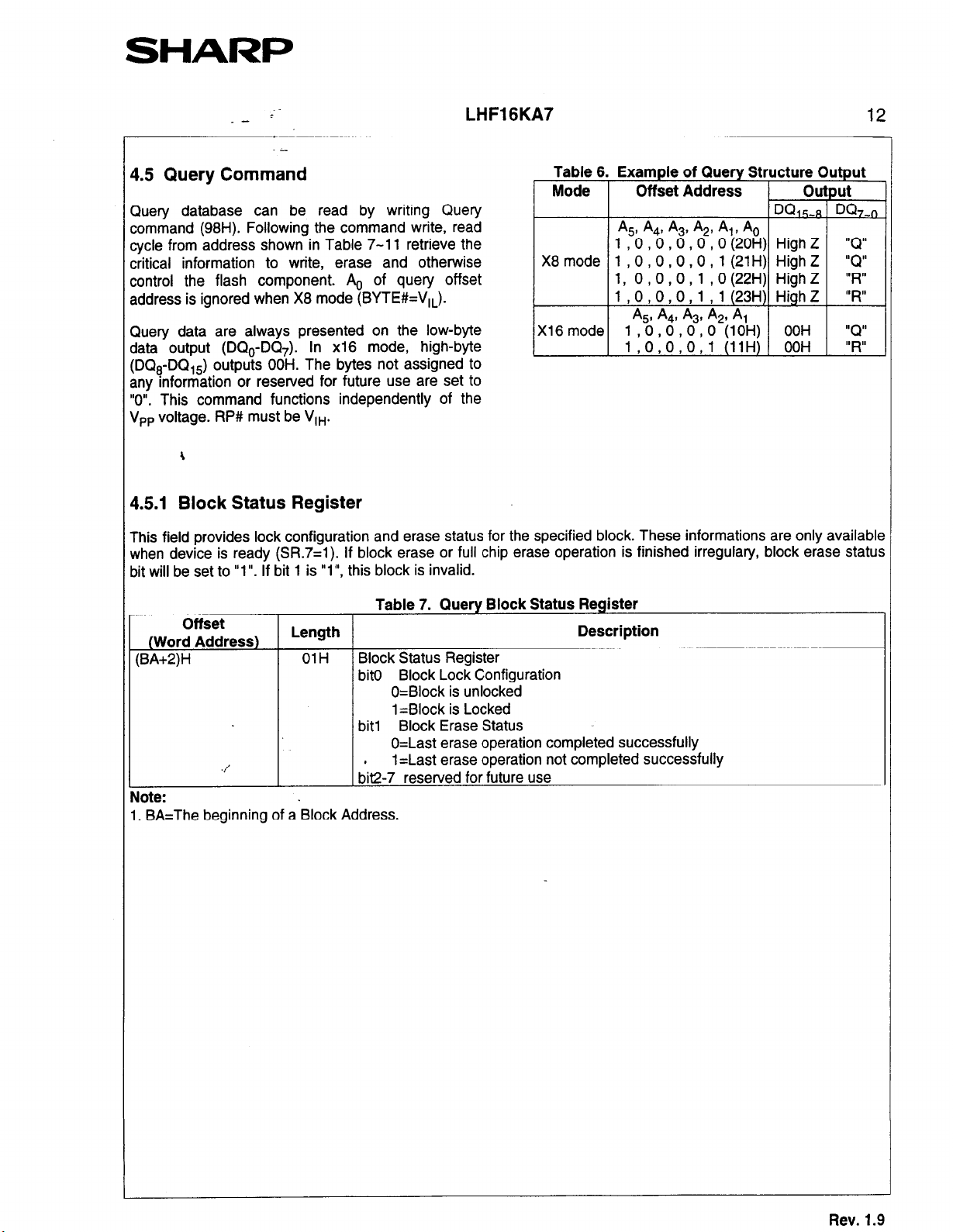
1.5 Query Command
=luery database can be read by writing Query
:ommand (98H). Following the command write, read
ycle from address shown in Table 7-l 1 retrieve the
xitical information to write, erase and otherwise
:ontrol the flash component. A, of query offset
address is ignored when X8 mode (BYTE#=V,L).
;luery data are always presented on the low-byte
jata output (DC&-D&). In x16 mode, high-byte
;DQs-DQ,s) outputs OOH. The bytes not assigned to
any information or reserved for future use are set to
‘0”. This command functions independently of the
Jpp voltage. RP# must be V,,.
Table 6. Example of Query Structure (
Mode Off set Address
A,, A,, A,, A,, A,, A,
1 , 0 , 0 , 0 (0 , 0 (20H) High Z
X8 mode 1 , 0 , 0 , 0 , 0 , 1 (21H) High Z
1, O,O,O,l ,0(22H) HighZ
1 , 0 , 0 , 0 , 1 , 1 (23H) High Z
A,, A,, A,, A,, A,
X16mode 1 ,O,O,O,O (10H) OOH
l,O,O,O,l (11H) OOH
ou
DQ%8
12
But
DQm-,
"Q"
"Q"
“R”
“R”
“Q”
“R”
1.5.1 Block Status Register
This field provides lock configuration and erase status for the specified block. These informations are only available
Nhen device is ready (SR.7=1). If block erase or full chip erase operation is finished irregulary, block erase status
lit will be set to “1”. If bit 1 is “l”, this block is invalid.
Table 7. Query Block Status Register
Offset
(Word Address)
(BA+2)H
v’
Uote:
I. BA=The beginning of a Block Address.
Length
OlH Block Status Register
bit0 Block Lock Configuration
O=Block is unlocked
1 =Block is Locked
bit1 Block Erase Status
O=Last erase operation completed successfully
1 =Last erase operation not completed successfully
t&2-7 reserved for future use
Description
Rev. 1.9
SHARP
_ -
LHFlGKA7
13
--
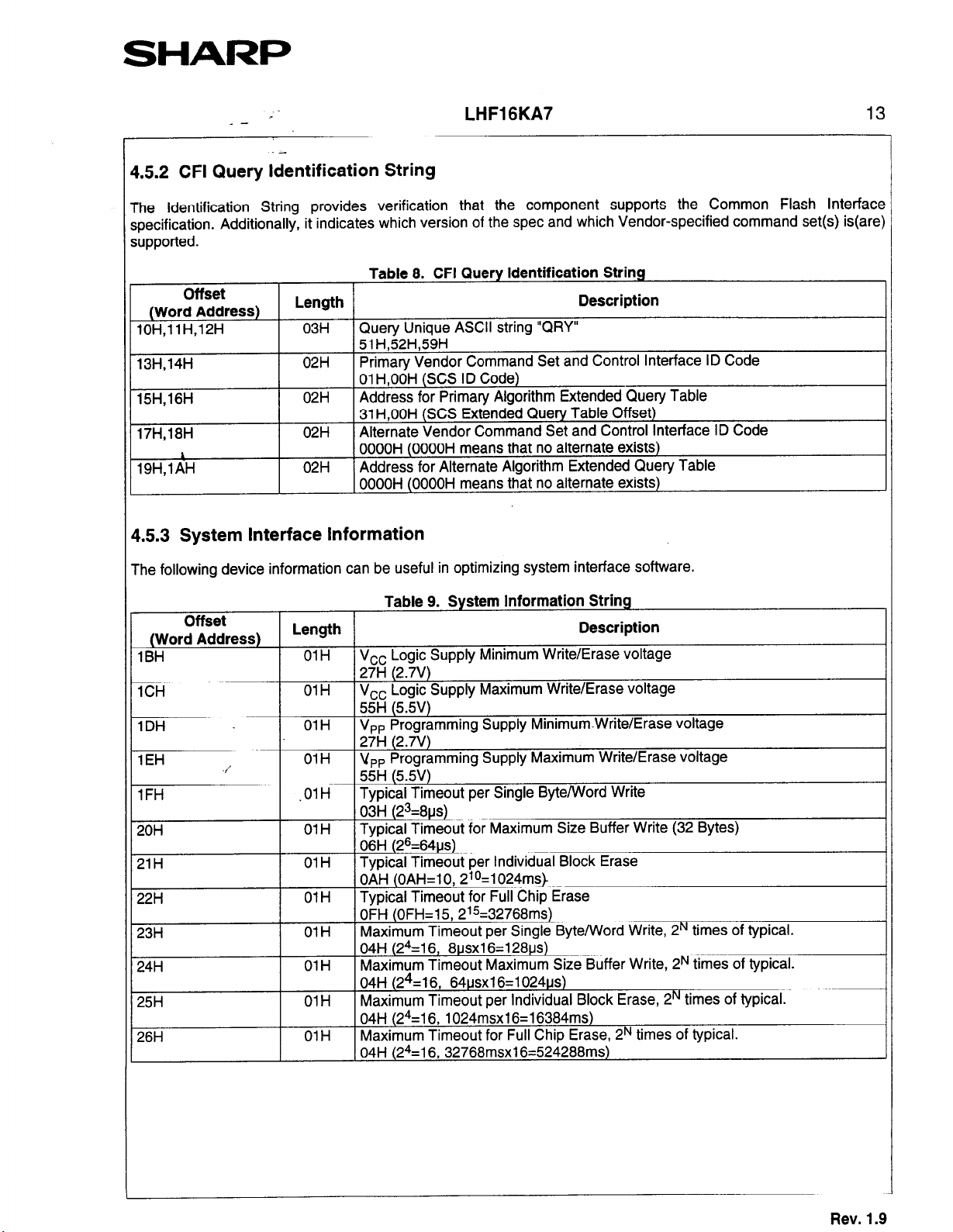
IS.2
CFI Query Identification String
‘he identification String provides verification that the component supports the Common Flash Interface
specification. Additionally, it indicates which version of the spec and which Vendor-specified command set(s) is(are)
upported.
Table 8. CFI Query Identification String
Offset
(Word Address)
lOH,l lH,12H
13H,14H
15H.16H
17H,18H
i
lSH,lAH
Length
03H Query Unique ASCII string “QRY”
51 H,52H,59H
02H
02H Address for Primary Algorithm Extended Query Table
02H
02H
Primary Vendor Command Set and Control Interface ID Code
01 H,OOH (SCS ID Code)
31 H,OOH (SCS Extended Query Table Offset)
Alternate Vendor Command Set and Control Interface ID Code
OOOOH (OOOOH means that no alternate exists)
Address for Alternate Algorithm Extended Query Table
1 OOOOH (OOOOH means that no alternate exists)
Description
1.53 System Interface Information
The following device information can be useful in optimizing system interface software.
Table 9. System Information String
Offset
(Word Address)
1BH
1CH
1DH OlH
1EH
1FH
20H
21H
22H
23H
24H
25H OlH
26H OlH Maximum Timeout for Full Chip Erase, 2N times of typical.
./’
Length
OlH
OlH V,, Logic Supply Maximum Write/Erase voltage
OlH
.OlH Typical Timeout per Single Byte/Word Write
1 01 H 1 Typical Timeout for Maximum Size Buffer Write (32
OlH Typical Timeout per Individual Block Erase
OlH Typical Timeout for Full Chip Erase
OlH Maximum Timeout per Single Byte/Word Write, 2N times of typical.
1 01
Voc Logic Supply Minimum Write/Erase voltage
27H (2.7V)
55H (5.5V)
V,, Programming Supply Minimum.Write/Erase voltage
27H (2.7V)
Up,, Programming Supply Maximum Write/Erase voltage
55H (5.5V)
I03H (23=8us)
06H (26=64us)
OAH (OAH=lO 21°=1024ms)
OFH (OFH=15, 215=32768ms)
I04H (24=1 6, 8usxl6=128us)
H
1 Maximum Timeout Maximum Size Buffer Write, 2N times of
04H (24=1 6, 64usxl6=1024us)
Maximum Timeout per Individual Block Erase, 2N times of typical.
04H (24=1 6,1024msxl6=16384ms)
I04H (24=1 6,32768msxl6=524288ms)
Description
Bytes)
_
typiCal.
Rev. 1.9
SHARI=
_ -
/
LHFlGKA7 14
.i
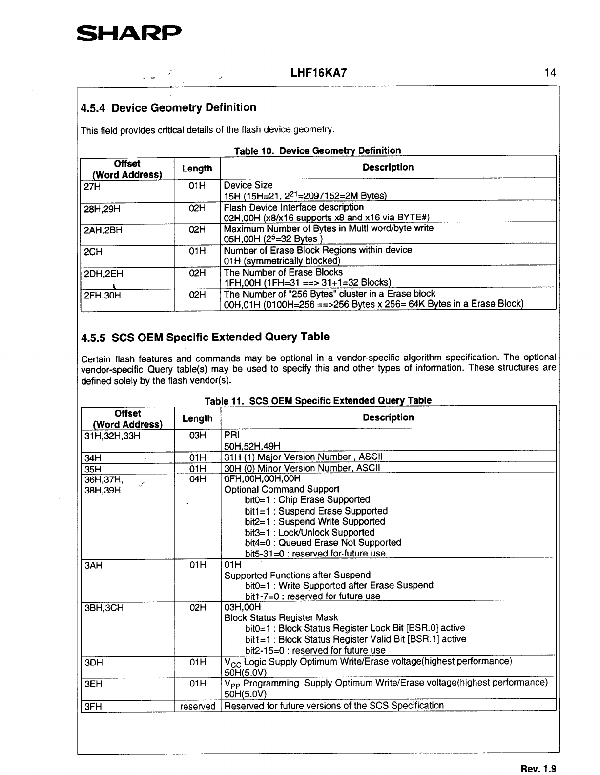
1.5.4 Device Geometry Definition
rhis field provides critical details of the flash device geometry.
Table 10. Device Geometry Definition
Offset
(Word Address)
27H
28H,29H
2AH,2BH
2CH
2DH,2EH
\
2FH,30H
Length
OlH Device Size
15H (15H=21,221=20971 52=2M Bytes)
02H
02H
01H
02H
02H
Flash Device Interface description
02H,OOH (x8/x16 supports x8 and xl 6 via BYTE#)
Maximum Number of Bytes in Multi word/byte write
05H,OOH (2s=32 Bytes )
Number of Erase Block Regions within device
01 H (symmetrically blocked)
The Number of Erase Blocks
1 FH,OOH (1 FH=31 ==> 31+1=32 Blocks)
The Number of “256 Bytes” cluster in a Erase block
, OOH,OlH (OlOOH=256 ==>256 Bytes x 256= 64K Bytes in a Erase Block)
1.5.5 SCS OEM Specific Extended Query Table
Description
Zertain flash features and commands may be optional in a vendor-specific algorithm specification. The optional
rendor-specific Query table(s) may be used to specify this and other types of information. These structures are
defined solely by the flash vendor(s).
Tat
e 11. SCS OEM Specific Extended Query Table
Offset
(Word Address)
31 H,32H,33H
38H,39H ”
3AH
3BH,3CH
3DH
3EH
3FH
Length
03H
OlH
OlH
04H OFH,OOH,OOH,OOH
OlH
02H
OlH
OlH
reserved
PRI
50H,52H,49H
31 H (1) Major Version Number , ASCII
30H (0) Minor Version Number, ASCII
Optional Command Support
bitO=l : Chip Erase Supported
bit1 =l : Suspend Erase Supported
bit2=1 : Suspend Write Supported
bit3=1 : Lock/Unlock Supported
bit4=0 : Queued Erase Not Supported
bit531 =O : reserved for-future use
OlH
Supported Functions after Suspend
bitO=l : Write Supported after Erase Suspend
bit1 -7=O : reserved for future use
03H,OOH
Block Status Register Mask
bitO=l : Block Status Register Lock Bit [BSR.O] active
bitl=l : Block Status Register Valid Bit [BSR.l] active
bit2-15=0 : reserved for future use
V,, Logic Supply Optimum Write/Erase voltage(highest performance)
50H@.OV)
Vpp Programming Supply Optimum Write/Erase voltage(highest performance)
56i-l(5.OV)
deserved for future versions of the SCS Specification
Description
Rev. 1.9
 Loading...