

Sharp LH28F160BJHE-TTL90 Datasheet

®
PRODUCT SPECIFICATIONS
Integrated Circuits Group
LH28F160BJHE-TTL90
Flash Memory
16M (1M × 16/2M × 8)
(Model No.: LHF16J04)
Spec No.: EL11X036
Issue Date: November 11, 1999
SliARP
LHF16504
l Handle this document carefully for it contains material protected by international copyright law.
Any reproduction, full or in part, of this material is prohibited without the express written
permission of the company.
l When using the products covered herein, please observe the conditions written herein and the
precautions outlined in the following paragraphs. In no event shall the company be liable for any
damages resulting from failure to strictly adhere to these conditions and precautions.
(1) The products covered herein are designed and manufactured for the following application
areas. When using the products covered herein for the equipment listed in Paragraph (2),
even for the following application areas, be sure to observe the precautions given in
Paragraph (2). Never use the products for the equipment listed in Paragraph (3).
*Office electronics
aInstrumentation and measuring equipment
@Machine tools
*Audiovisual equipment
*Home appliance
l Com’munication equipment other than for trunk lines
(2) Those contemplating using the products covered herein for the following equipment which
demands hiuh reliabilitv, should first contact a sales representative of the company and then
accept responsibility for incorporatin,
other appropriate measures for ensuring reliability and safety of the equipment and the
overall system.
@Control and safety devices for airplanes, trains, automobiles, and other
transportation equipment
*Mainframe computers
@Traffic control systems
*Gas leak detectors and automatic cutoff devices
*Rescue and security equipment’
aOther safety devices and safety equipment, etc.
(3) Do not use the products covered herein for the following equipment which demands
extremely high oerformance in terms of functionality, reliability, or accuracy.
aAerospace equipment
*Communications equipment for trunk lines
*Control equipment for the nuclear power industry
*Medical equipment related to life support, etc.
(4) Please direct all queries and comments regardin,
Paragraphs to a sales representative of the company.
0 into the design fail-safe operation, redundancy, and
0 the interpretation of the above three
l Please direct all queries regardin,
company.
0 the products covered herein to a sales representative of the
Rev. 1.15
SHARP
LHFl6504
CONTENTS
PAGE
INTRODUCTION.. ............................................................ 3
1.1 Features ........................................................................ 3
1.2 Product Overview..
1.3 Product Description.. ................................................... .4
1.3.1 Package Pinout ...................................................... .4
1.3.2 Block Organization.. ............................................... 4
PRINCIPLES OF OPERATION.. ...................................... 7
2.1 Data Protection.. .......................................................... .8
BUS OPERATION
3.1 Read .............................................................................. 8
3.2 Output Disable
3.3 Standby.. ....................................................................... 8
3.4 Reset ............................................................................. 8
3.5 Read Identifier Codes.. ................................................ .9
3.6 Write.. ..........................................................................
COMMAND DEFINITIONS ............................................. 9
4.1 Read Array Command.. .............................................. 12
4.2 Read
4.3 Read Status Register Command.. ............................... 12
4.4 Clear Status Register Command..
4.5 Block Erase Command..
4.6 Full Chip Erase
4.7 Word/Byte Write Command.. ..................................... 13
4.8 Block Erase Suspend Command ................................ I4
4.9 Word/Byte Write Suspend Command..
4.10 Set Block and Permanent Lock-Bit Command.. ....... I5
4.1 1 Clear Block Lock-Bits Command
4.12 Block Locking by the WP#
Identifier Codes Command ............................... 12
....................................................... 3
............................................................ 8
.............................................................. 8
.9
...............................
............................................. 13
Command ......................................... 13
......................
............................ 15
......................................
12
14
16
PAGE
5 DESIGN CONSIDERATIONS ....................................... 25
5.1 Three-Line Output Control
5.2 RY/BY# and WSM Polling .......................................
5.3 Power Supply Decoupling
5.4 Vccw Trace on Printed Circuit Boards
5.5 v,, . vccw.
5.6 Power-Up/Down
5.7 Power Dissipation
5.8 Data Protection Method
6 ELECTRICAL SPECIFICATIONS ................................
6.1 Absolute Maximum Ratings..
6.2 Operating Conditions .................................................
6.2.1 Capacitance
AC Input/Output Test Conditions.. ...................... 28
6.2.2
6.2.3 DC Characteristics ............................................... 29
6.2.4 AC Characteristics - Read-Only Operations..
6.2.5 AC Characteristics - Write Operations
6.2.6 Alternative CE#-Controlled Writes
6.2.7 Reset Operations
6.2.8 Block Erase. Full Chip Erase, Word/Byte Write and
Lock-Bit Configuration Performance ................. 39
7 PACKAGE AND PACKING SPECIFICATIONS
RP# Transitions .................................... 25
Protection.. ..................................... 26
...................................................... 26
.......................................................... 27
........................................ 25
25
......................................... 25
..................... 25
............................................. 26
27
.................................... 27
27
...... 31
................ 34
...................... 36
.................................................. 38
.......... 40
1
Rev. 1.25
LI-IFI 6504
LH28F 160B JHE-TTL90
2
IGM-BIT ( 1Mbit x16 / 2Mbit
Boot Block Flash MEMORY
n Low Voltage Operation
- v,,=v(-cw-L.
n User-Configurable x8 or x 16 Operation
n High-Performance Read Access Time
- 90ns(Vcc=2.7V-3.6V)
n Operating Temperature
- -40°C to +85”C
I Low Power Management
-
Typ. 2uA (V,,=3,OV) Standby Current
-
Automatic Power Savings Mode Decreases ICCR in
Static Mode
- Typ. 120pA (V,,=3.OV, T,=+25”C. f=32kHz)
Read Current
n Optimized Array Blocking Architecture
-
Two 4K-word (8K-byte) Boot Blocks
-
Six 4K-word (8K-byte) Parameter Blocks
-
Thirty-one 32K-word (64K-byte) Main Blocks
- Top Boot Location
n Extended Cycling Capability
-
Minimum 100,000 Block Erase Cycles
-’ 7V-3.6V Single Voltage
x8
)
H Enhanced Automated Suspend Options
-
Word/Byte Write Suspend to Read
-
Block Erase Suspend to Word/Byte Write
-
Block Erase Suspend to Read
n Enhanced Data Protection Features
-
Absolute Protection with VCCWIVCCWLK
-
Block Erase, Full Chip Erase, Word/Byte Write and
Lock-Bit Configuration Lockout during Power
Transitions
-
Block Locking with Command and WP#
-
Permanent Locking
n
Automated Block Erase, Full Chip Erase,
Word/Byte Write and Lock-Bit Configuration
-
Command User Interface (CUB
-
Status Register (SR)
n SRAM-Compatible Write Interface
n Industry-Standard Packaging
-
G-Lead TSOP
n ETOXTkt* Nonvolatile Flash Technology
W CMOS Process (P-type silicon substrate)
w Not designed or rated as radiation hardened
iHARP’s LH28F160BJHE-TTL90 Flash memory is a high-density. low-cost. nonvolatile, read/write storage solution for a
vide range of applications.
,H28F160BJHE-TTL90 can operate at V,,=2.7V-3.6V and Vc-w--.
:apability realize battery life and suits for cellular phone application.
ts Boot, Parameter and Main-blocked architecture, low voltage and extended cycling provide for highly flexible component
uitable for portable terminals and personal computers. Its enhanced suspend capabilities provide for an ideal solution for code
- data storage applications.
:or secure code storage applications, such as networking, where code is either directly executed out of flash or downloaded to
IRAM, the LH28F160BJHE-TTL90 offers four levels of protection: absolute protection with VccwlVc-wLK, selective
lardware block locking or flexible software block locking. These alternatives Z
ecurity needs.
he LH28F160BJHE-‘ITL90 is manufactured on SHARP’s 0.25pm ETOXT”*
tandard package: the 4%lead TSOP, ideal for board constrained applications.
ETOX is a trademark of Intel Corporation.
-3 TV-3.6V or 11.7V-12.3V. Its low voltage operation
oive designers ultimate control of their code
process technology. It come in industry-
Rev. 1.25
SHARP
LHF16504
1 INTRODUCTION
This
specifications. Section 1 provides a flash memory
overview. Sections 2. 3. 4 and 5 describe the memory
organization and functionality. Section 6 covers electrical
specifications.
datasheet
contains
LH28F160BJHE-T-IL90
1.1 Features
Key enhancements of LH28F16OBJHE-TTL90 boot block
Flash memory are:
Gingle low voltage operation
*Low power consumption
*Enhanced Suspend Capabilities
l Boot Block Architecture
Please note following:
l
VCCWLK has been lowered to l.OV to support 2.7V-
3.6V block erase. full chip erase. word/byte write and
lock-bit configuration operations. The Vccw voltage
transitions to GND is recommended for designs that
switch Vccw off during read operation.
1.2 Product Overview
The LH28F160BJHE-TTL90 is a high-performance 16Mait Boot Block Flash memory organized as lM-word of 16
aits or 2M-byte of 8 bits. The lM-word/2M-byte of data is
u-ranged in two 4K-word/SK-byte boot blocks, six 4Kword/8K-byte parameter blocks and thirty-one 32Kvord/64K-byte main blocks which are individually
:rasable, lockable and unlockable in-system. The memory
nap is shown in Figure 3.
Ihe dedicated V ccw pin gives complete data protection
vhen V
CCW’VCCWLK.
4 Command User Interface (CUD serves as the interface
jetween the system processor and internal operation of the
ievice. A valid command sequence written to the CUI
nitiates device automation. An internal Write State
vlachine (WSM) automatically executes the algorithms
md timings necessary for block erase, full chip erase.
vord/byte write and lock-bit configuration operations.
3
A block erase operation erases one of the device’s 32K-
word/6JK-byte blocks typically within 1.2s (3V Vcc. 3V
ccw). JK-word/8K-byte blocks typically within 0.6s (3V
V
V,,. 3V Vccw) independent of other blocks. Each block
can be independently erased minimum 100,000 times.
Block erase suspend mode allows system software to
suspend block erase to read or write data from any other
block.
Writing memory data is performed in word/byte
increments of the device’s 32K-word blocks typically
within 33~s (3V V,,. 3V Vccw). 6JK-byte blocks
typically within 31~s (3V V,,. 3V Vccw). 4K-word
blocks typically within 36~s (3V Vcc. 3V V,,,), 8Kbyte blocks typically within 32~s (3V Vcc. 3V Vccw).
Word/byte write suspend mode enables the system to read
data or execute code from any other flash memory array
location.
Individual block locking uses a combination of bits, thirty-
nine block lock-bits. a permanent lock-bit and WP# pin. to
lock and unlock blocks. Block lock-bits gate block erase.
full chip erase and word/byte write operations. while the
permanent lock-bit pates block lock-bit modification and
locked block alternation. Lock-bit configuration
operations (Set Block Lock-Bit, Set Permanent Lock-Bit
and Clear Block Lock-Bits commands) set and cleared
lock-bits.
The status register indicates when the WSM‘s block erase,
fuli chip erase. word/byte write or lock-bit configuration
operation is finished.
The RY/BY# output gives an additional indicator of WSM
activity by providing both a hardware signal of status
(versus software polling) and status masking (interrupt
masking for background block erase, for example). Status
polling using RY/BY# minimizes both CPU overhead and
system power consumption. When low, RY/BY# indicates
that the WSM is performing a block erase. full chip erase.
word/byte write or lock-bit configuration. RY/BY#-high Z
indicates that the WSIM is ready for a new command.
block erase is suspended (and word/byte write is
inactive), word/byte write is suspended. or the device is in
reset mode.
1
Rev. 1.25
LHFl6504
4
The access time is 90ns (tAv v) over the operating
temperature range (-40°C to + 5°C) 8 and V,- supply
voltage range of 2.7V-3.6V.
The Automatic Power Savings (APS) feature substantially
reduces active current when the device is in static mode
(addresses not switching). In APS mode, the typicaJ ICCR
current is 2pA (CMOS) at 3.OV V,,.
When CE# and RP# pins are at V,-. the I,, CMOS
standby mode is enabled. When the RP# pin is at GND,
reset
mode is enabled which minimizes power
consumption and provides write protection. A reset time
(tpHQv) is required from RP# switching high until outputs
are valid. Likewise, the device has a wake time (tpHEL)
from RP#-high until writes to the CljI are recognized.
With RP# at GND, the WSM is reset and the status
register is cleared.
Please do not
has already been programed “0”. Overwrite operation may
generate unerasable bit. In case of reprogramming “0” to
the data which has been programed “1”.
.Prograrn “0” for the bit in which you want to change
data from ” 1” to “0”.
.Program “1” for the bit which has already been
programmed “0”.
For example, changing data from “10111101” to
‘10111100” requires “11111110” programming.
execute
reprogramming “0” for the bit which
1.3 Product Description
1.3.1 Package Pinout
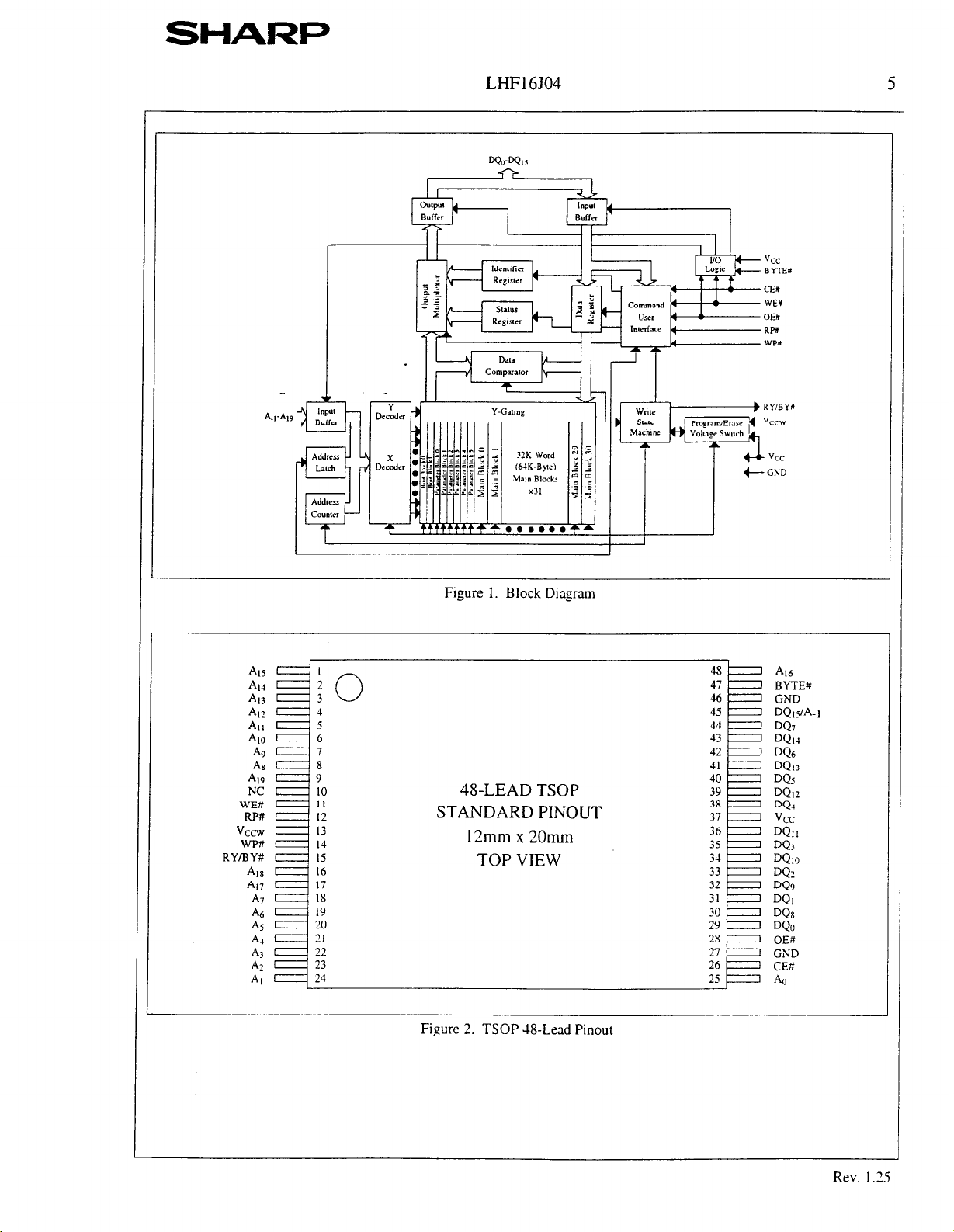
LH28F160BJHE-TTL90 Boot Block Flash memory is
available in J8-lead TSOP package (see Figure 2).
1.32 Block Organization
This product features an asymmetrically-blocked
architecture providing system memory integration. Each
erase block can be erased independently of the others up to
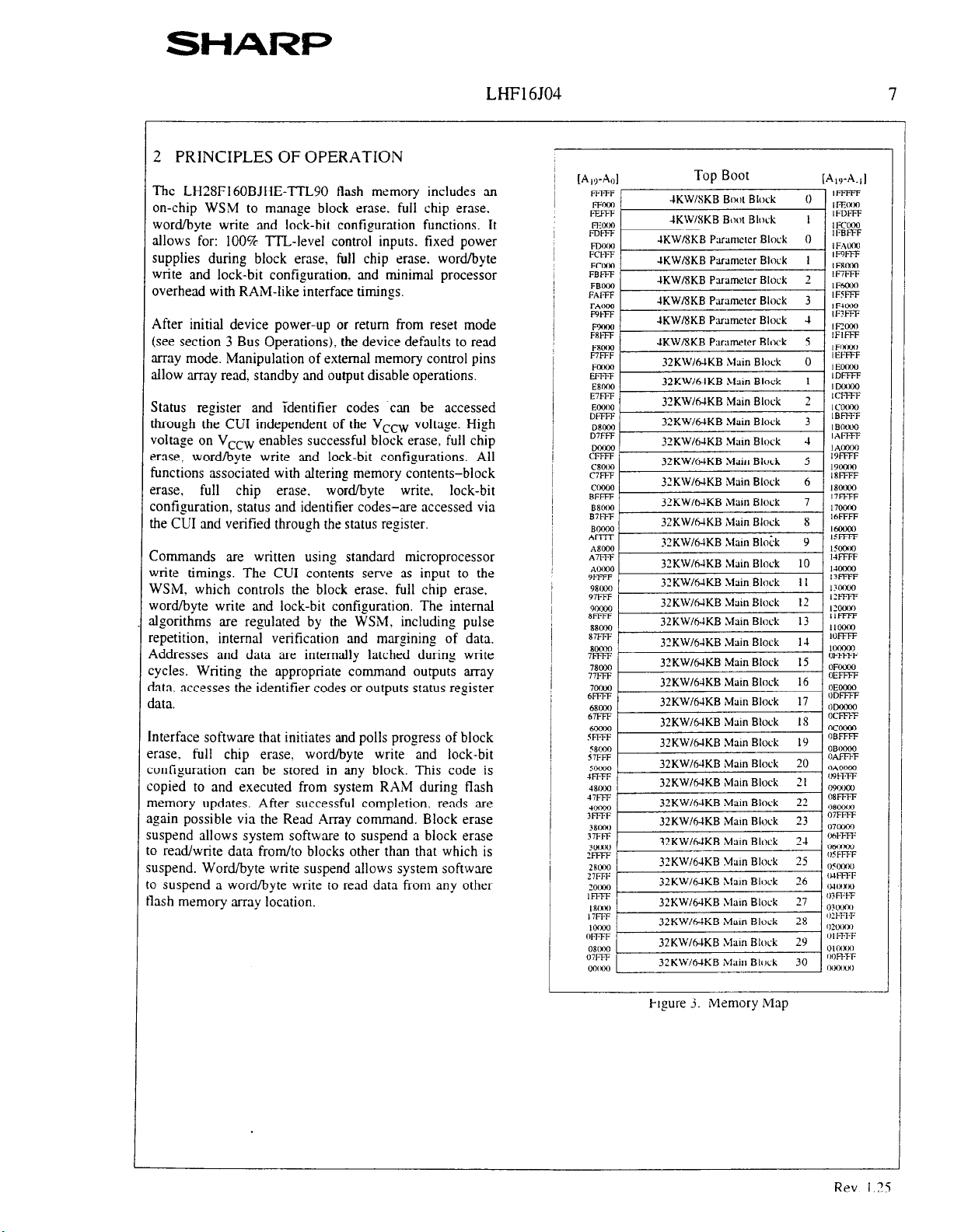
100,000 times. For the address locations of the blocks. see
the memory map in Figure 3.
Boot Blocks: The boot block is intended to replace a
dedicated boot PROM in a microprocessor or
microcontroller-based system. This boot block 4K words
(4.096words) features hardware controllable write-
protection to protect the crucial microprocessor boot code
from accidental modification. The protection of the boot
block is controlled using a combination of the Vccw, RP#.
WP# pins and block lock-bit.
Parameter Blocks: The boot block architecture includes
parameter blocks to facilitate storage of frequently update
small parameters that would normally require an
EEPROM. By using software techniques. the word-rewrite
functionality of EEPROMs can be emulated. Each boot
block component contains six parameter blocks of 4K
words (4.096 words) each. The protection of the parameter
block is controlled using a combination of the Vccw. RP#
and block lock-bit.
Main Blocks: The reminder is divided into main blocks for
data
or
code storage.
one 32K words (32,768 words) blocks. The protection of
the main block is controlled using a combination of the
Vccw, RP#
and
Each 16M-bit device contains thirty-
block lock-bit.
Rev. 1.25
SHARI=
LHF16504 5
CEY
WEX
OEX
RF?+
Buffer h /
WE#
RP#
vccw
WP#
RYlBY#
Al5
Al4
A13
A12
All
40
A9
‘48
49
NC
‘418
A17
A7
%
A5
A.,
A3
A2
Al
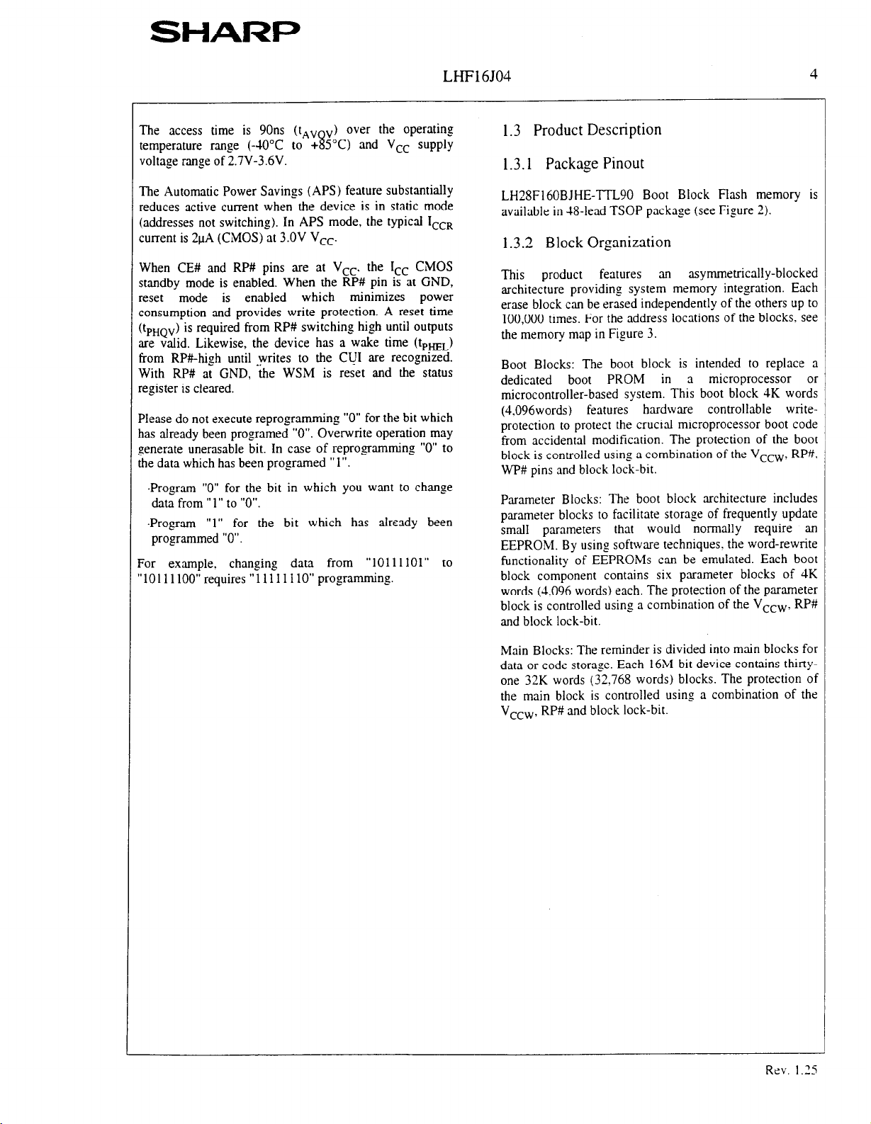
Figure 1. Block Diagram
4%LEAD TSOP
STANDARD PINOUT
12mm x 20mm
TOP VIEW
Figure 2. TSOP -%Lead Pinout
A16
BYTE?4
GND
DQJA-I
DQ7
DQu
DQ6
DQu
DQ5
DQlr
DQa
vcc
DQII
DQ3
DQIO
DQz
DQ!,
DQI
DQs
DQo
OE#
GND
CE#
A0
Rev. 1.25
LHFl6JO4
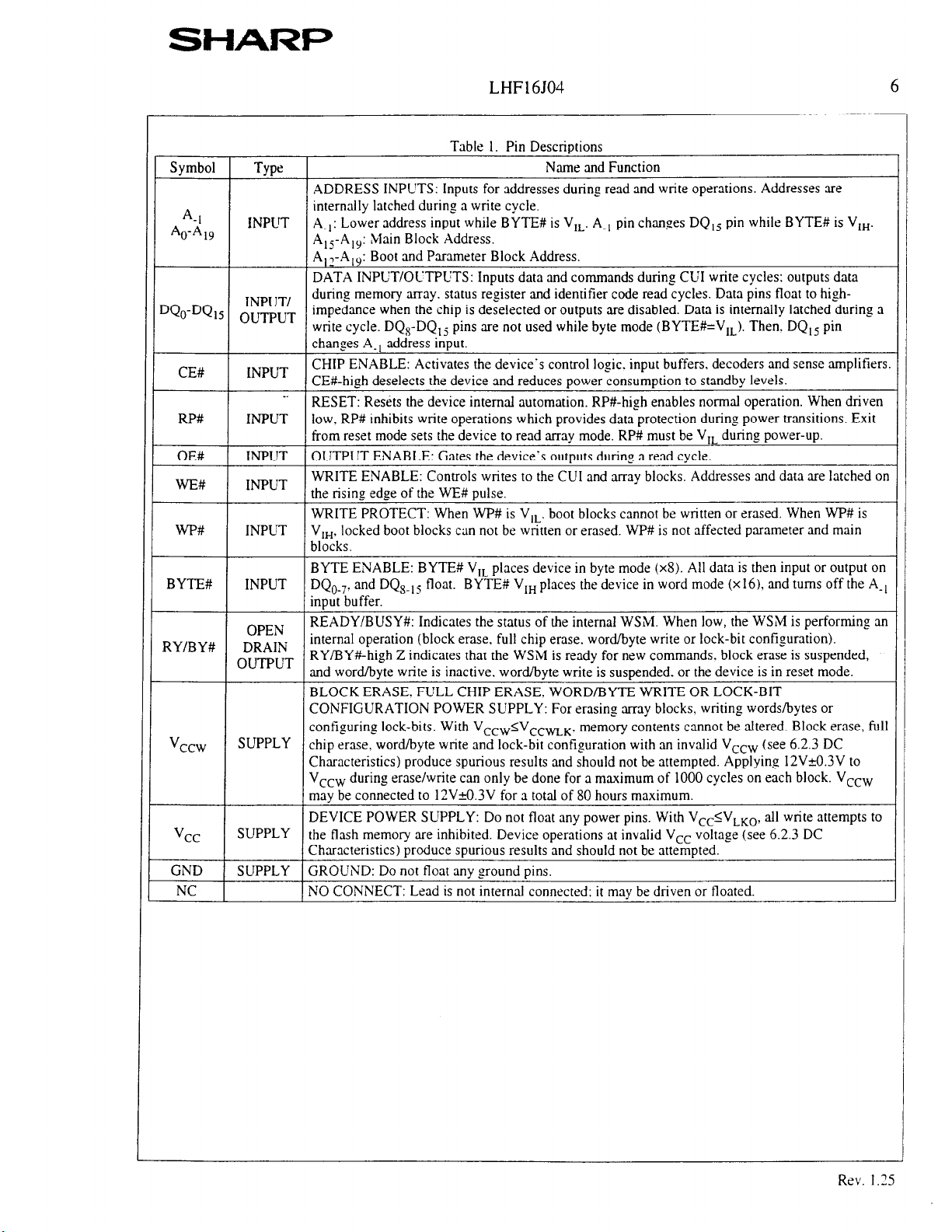
Table 1. Pin Descriptions
Symbol
A-1
A,-‘419
"Qo-DQ,,
CE#
RP#
OE#
WE#
WP#
BYTE# INPUT DQO-,. and DQ,., j float. BYTE# V,, places the device in word mode (x16), and turns off the A-,
RY/BY# DRAIN
Vccw
vcc
GND SUPPLY GROUND: Do not float any ground pins.
NC NO CONNECT: Lead is not internal connected: it may be driven or floated.
Type
ADDRESS INPUTS: Inputs for addresses during read and write operations. Addresses are
internally latched during a write cycle.
INPUT A-,: Lower address input while BYTE# is V,,. A-, pin changes DQ, j pin while BYTE# is Vt,.
A, j-A,,: Main Block Address.
A,,-A,,: Boot and Parameter Block Address.
DATA INPUT/OUTPUTS: Inputs data and commands during CUI write cycles: outputs data
INPUT/
OUTpUT
INPUT
INPUT low. RP# inhibits write operations which provides data protection during power transitions. Exit
INPUT
INPUT
INPUT V,,, locked boot blocks can not be written or erased. WP# is not affected parameter and main
OPEN
OUTPUT
SUPPLY
SUPPLY the flash memory are inhibited. Device operations at invalid V,, voltage (see 6.2.3 DC
during memory array. status register and identifier code read cycles. Data pins float to highimpedance when the chip is deselected or outputs are disabled. Data is internally latched during a
write cycle. DQs-DQ, j pins are not used while byte mode (BYTE#=V,,). Then. DQls pin
changes A-, address input.
CHIP ENABLE: Activates the device’s control logic. input buffers. decoders and sense amplifiers.
CE#-high deselects the device and reduces power consumption to standby levels.
_.
RESET: Resets the device internal automation. RP#-high enables normal operation. When driven
from reset mode sets the device to read array mode. RP# must be V,, during power-up.
OUTPUT ENABLE: Gates the device’s outputs during a read cycle.
WRITE ENABLE: Controls writes to the CUI and array blocks. Addresses and data are latched on
the rising edge of the WE# pulse.
WRITE PROTECT: When WP# is V,,. boot blocks cannot be written or erased. When WP# is
blocks.
BYTE ENABLE: BYTE# V,, places device in byte mode (x8). All data is then input or output on
input buffer.
READY/BUSY#: Indicates the status of the internal WSM. When low, the WSM is performing an
internal operation (block erase. full chip erase. word/byte write or lock-bit configuration).
RY/BY#-high Z indicates that the WSM is ready for new commands. block erase is suspended,
and word/byte write is inactive. word/byte write is suspended. or the device is in reset mode.
BLOCK ERASE. FULL CHIP ERASE. WORD/BYTE WRITE OR LOCK-BIT
CONFIGURATION POWER SUPPLY: For erasing array blocks, writing words/bytes or
configuring lock-bits. With VCCW<VCCWLK.
chip erase, word/byte write and lock-bit configuration with an invalid V,--w (see 6.2.3 DC
Characteristics) produce spurious results and should not be attempted. Applying 12Va0.3V to
Vc-w during erase/write can only be done for a maximum of 1000 cycles on each block. V,,,
may be connected to 12V@.3V for a total of 80 hours maximum.
DEVICE POWER SUPPLY: Do not float any power pins. With V&V,,,, all write attempts to
Characteristics) produce spurious results and should not be attempted.
Name and Function
memory contents cannot be altered. Block erase, full
6
Rev. 1.25
SHARI’=
LHFI 6504 7
2 PRINCIPLES OF OPERATION
The LH?8F160BJHE-TTL90
on-chip WSM to manage block erase. full chip erase.
wordlbyte write and lock-bit configuration functions. It
allows for: 100% TILleve control inputs. fixed power
supplies during block erase, full chip erase. word/byte
write and lock-bit configuration. and minimal processor
overhead with RAIM-like interface timings.
After initial device power-up or return from reset mode
(see section 3 Bus Operations), the device defaults to read
array mode. Manipulation of external memory control pins
allow array read, standby and output disable operations.
Status register and identifier codes can be accessed
through the CUI independent of the Vccw voltage. High
voltage on Vccw enables successful block erase, full chip
erase, word/byte write and lock-bit configurations. All
functions associated with altering memory contents-block
:rase, full chip erase. word/byte write. lock-bit
:onfiguration, status and identifier codes-are accessed via
he CUI and verified through the status register.
Commands are written using standard microprocessor
vrite timings. The CUI contents serve as input to the
WSM, which controls the block erase. full chip erase,
vord/byte write and lock-bit configuration. The internal
tlgorithms are regulated by the WSM, including pulse
,epetition, internal verification and margining of data.
iddresses and data are internally latched during write
:ycles. Writing the appropriate command outputs array
lata. accesses the identifier codes or outputs status register
lata.
nterface software that initiates and polls progress of block
‘rase. full chip erase, word/byte write and lock-bit
onfiguration can be stored in any block. This code is
opied to and executed from system RAIM during flash
nemory updates.
After successful
gain possible via the Read Array command. Block erase
uspend allows system software to suspend a block erase
I read/write data from/to blocks other than that which is
uspend. Word/byte write suspend allows system software
I suspend a word/byte write to read data from any other
lash memory array location.
flash memory includes an
completion, reads are
[AII-&II
FtlTF
FFm
FE.
Flilx4
rnr7+
mow
FCtFF
FCMI
FBWF
FBCW
FAFFF
FAlKK?
F9tFF
FW”,,
FRWF
FPIIXK)
RFFF
FM*)
EFFFF
E8MO
E7FFF
Eixml
DFFFF
D8D00
D7WF
c%
C8cix)
c7m
ET?=
B8Nx)
B7tFF
BOOM)
AFFFF
A8033
Am
AcmO
9tFFF
98wxl
97FFF
9MXJ
WFFF
88mo
87FFF
8oIx)t)
7FFFF
780X
77m
7oM
6FFFF
68oMl
67FFF
5Fkz
58Mo
57FFF
5OlXKl
JFFFF
48*M
J7FFF
:I
38mi,
37FFF
3otml
FFFF
28ooo
27FFF
XOXJ
IFFFF
,R,XX,
I7FFT
IIWX
OFFFF
“8MM
“7FFF
OO~KHI
Top Boot
B
Main
Block
32KWlhAKB Mam Block 23
32KW/6-lKB Xlam Block
32KWNKB ,Mun Block 28
Figure 3. Memory ~Map
Rev. 1.35
SHARP
LHFl6504
2.1 Data Protection
Wkn vccw~vccw,,~
altered. The GUI. with two-step block erase. full chip
erase. word/byte write or lock-bit configuration command
sequences, provides protection from unwanted operations
even when high voltage is applied to Vccw. All write
functions are disabled when Vcc is below the write
lockout voltage VLKO or when RP# is at V,,. The device’s
block locking capability provides additional protection
from inadvertent code or data alteration by gating block
erase, full chip erase and word/byte write operations.
Refer to Table 5 for write protection alternatives.
memory contents cannot be
3 BUS OPERATlON
l3e local CPU reads and writes flash memory in-system.
411
bus cycles to or from the flash memory conform to
standard microprocessor bus cycles.
3.1 Read
nformation can be read from any block. identifier codes
)r status register independent of the Vccw voltage. RP#
:an be at V,,.
i-he first task is to write the appropriate read mode
:ommand (Read Array, Read Identifier Codes or Read
itatus Register) to the GUI. Upon initial device power-up
jr after exit from reset mode, the device automatically
esets to read array mode. Six control pins dictate the data
low in and out of the component: CE#. OE#. BYTE#,
JZ#, RP# and WP#. CE# and OE# must be driven active
3 obtain data at the outputs. CE# is the device selection
ontrol. and when active enables the selected memory
evice. OE# is the data output (DQ,-DQlj) control and
{hen active drives the selected memory data onto the l/O
us. BYTE# is the device l/O interface mode control.
VE# must be at V,,, RP# must be at V,,. and BYTE#
nd WP# must be at V,,
:ad cycle.
2 Output
v’ith OE# at a logic-high level (VI,), the device outputs
re disabled. Output pins (DQ,-DQ,,) are placed in a
igh-impedance state.
Disable
or V,,. Figure 14. 15 illustrates
8
3.3 Standby
CE# a.t a logic-high level (V,,) places the device ir
standby mode which substantially reduces device powel
consumption. DQ,-DQ,, outputs are placed in a highimpedance state independent of OE#. If deselected during
block erase, full chip erase, word/byte write or lock-bil
confi,ouration, the device continues functioning, ant
consuming active power until the operation completes.
3.4 Reset
RP# at V,, initiates the reset mode.
In read modes, RP#-low deselects the memory. places
output drivers in a high-impedance state and turns off all
internal circuits. RP# must be held low for a minimum ot
IOOns. Time tpHQV
mode until initial memory access outputs are valid. After
this wake-up interval. normal operation is restored. The
GUI is reset to read array mode and status register is set to
80H.
During block erase. full chip erase, word/byte write or
lock-bit configuradon modes. RP#-low will abort the
operation. RY/E%Y# remains low until the reset operation
is complete. Memory contents being altered are no longer
valid; the data may be partially erased or written. Time
tpmvL is required after RP# goes to logic-high (VIH)
before another command can be written.
As with any automated device, it is important to assert
RP# during system reset. When the system comes out of
reset, it expects to read from the flash memory. Automated
flash memories provide status information when accessed
during block erase. full chip erase. word/byte write or
lock-bit configuration modes. If a CPU reset occurs with
no flash memory reset. proper CPU initialization may not
occur because the flash memory may be providing status
information instead of array data. SHARP’s flash
memories allow proper CPU initialization following a
system reset through the use of the RP# input. In this
application. RP# is controlled by the same RESET# signal
that resets the system CPU.
is required after return from reset
Rev. 1.25
SHARP
I:::_::_::::::
LHFl6504
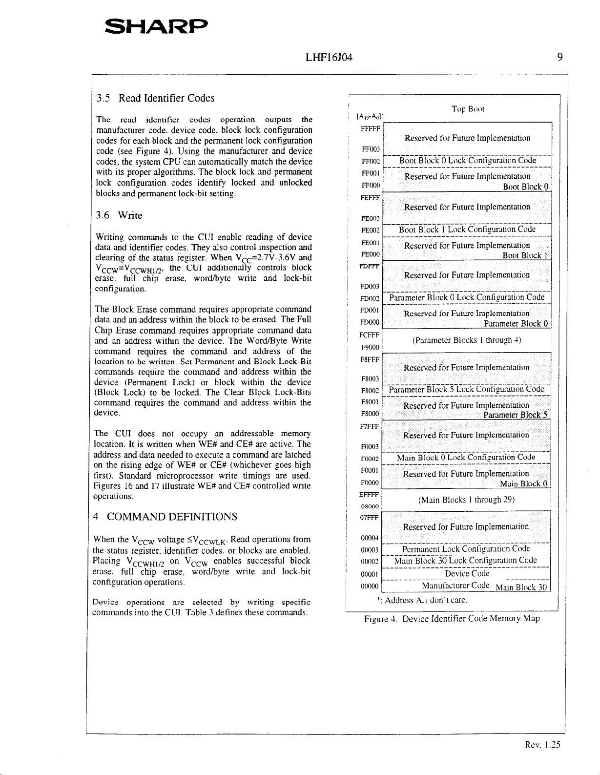
3.5 Read Identifier Codes
The read identifier codes operation outputs the
manufacturer
codes for each block and the permanent lock configuration
code (see Figure 4). Using the manufacturer and device
codes. the system CPU can automatically match the device
with its proper algorithms. The block lock and permanent
lock configuration codes identify locked and unlocked
blocks and permanent lock-bit settin:.
code.
device code. block lock configuration
3.6 Write
Writing commands to the CUI enable reading of device
data
and
identifier codes. They also control inspection and
clearing of the status register. When V&=2.7V-3.6V and
V
CCW=VCCWHIR)
erase. full chip erase, word/byte write and lock-bit
configuration.
The Block Erase command requires appropriate command
data and an address within the block to be erased. The Full
Chip Erase command requires appropriate command data
and
an address within the device. The Word/Byte Write
command requires the command and address of the
location to be written. Set Permanent and Block Lock-Bit
commands require the command and address within the
zlevice (Permanent Lock) or block within the device
iBlock Lock) to be locked. The Clear Block Lock-Bits
:ommand requires the command and address within the
levice.
lhe CUI does not occupy an addressable memory
ocation. It is written when WE# and CE# are active. The
iddress and data needed to execute a command are latched
)n the rising
‘First). Standard microprocessor write timings are used.
?gures 16 and 17 illustrate WE# and CE# controlled write
operations.
t COMMAND DEFINITIONS
Nhen the VCcw voltage IV,,,,. Read operations from
he
status
register, identifier codes. or blocks are enabled.
‘lacing VCCWH,,2 on VCCw enables successful block
:rase. full chip erase. word/byte write and lock-bit
configuration operations.
device operations are selected by writing specific
ommands into the CUI. Table 3 defines these commands.
the CUI additionally controls block
edge
of WE# or CE# (whichever goes high
FFFFFf
Reserved for Future Implementation
FFrm
I
_______________-----------------------
FFOOZ
FFOOI
FFOOO
FEFFF
FE003
FE002
FDOOl
FDmil
FCFFF ;
FW,-!il !
. ,.I--
FXOO?
F8001
F8000
F7FFF
FOO03
EFFFF:
“----
07FFF
00004
00003
OOOO?
0000 I
00000 Manufacturer Code Main Block
Figure 4. Device Identifier Code Memory .Map
Boot Block 0 Lock Conliguration Co&
_________------------~~~~~~~~~~~~~~~~~
Reserved for Future Implementation
Boot Block 0
Reserved for Future Implementation
_____________ ------- ---------- ------
Boot Block 1 Lock Conlieuration Code
__________---------------_----_-
Reserved for Future Implementation
(Parameter Blocks I through -I)
Reserved for Future Implementation
_--_-______-__-___-_------------------
Reserved for Future ImpIementation
Reserved for Future Implementation
(Main Blocks 1 through 29)
Reserved for Future Implementation
Permanent Lock Conligrration Code
Main Block 30 Lock Configuration Code
____________________------------------
*: Address A.1 don‘t care.
Device Code
Parameter Block 0
-
Parameter Block 5
9
1
I
j[J
Rev. 1.25
SHAl?P
Read Identifier Codes
LHFl6J04
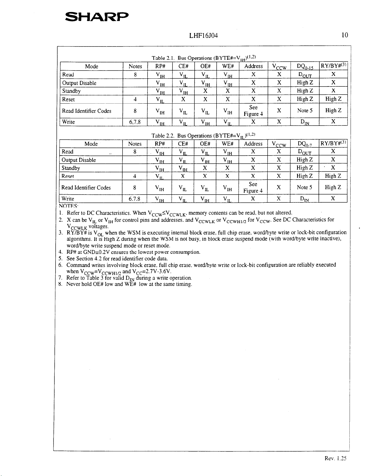
Table 2.1. Bus Onerations (BYTE#=V,U)tt+z)
Write 1 6.7.8
VOTES:
1. Refer to DC Characteristics. When V,-,wIV,,w,,. memory contents can be read. but not altered.
2. X can be V,, or V,, for control pins and addresses. and V,,,,, or V,,,,,,? for Vccw. See DC Characteristics for
VCCwLK voltages.
3. RY/BY# is V,, when the WSM is executing internal block erase. full chip erase, word/byte write or lock-bit configuration
algorithms. It is High Z during when the WSIM is not busy, in block erase suspend mode (with word/byte write inactive),
word/byte write suspend mode or reset mode.
4. RP# at GNDk0.2V ensures the lowest power consumption.
5. See Section 4.2 for read identifier code data.
6. Command writes involving block erase. full chip erase. word/byte write or lock-bit configuration are reliably executed
when VCCw=VCCWHln and V,-,=2.7V-3.6V.
7. Refer to Table 3 for valid Dt, during a write operation.
8. Never hold OE# low and WE# low at the same timing.
VI, VI, VI, VI,
X
DIN
X
Rev. 1.25
SHARP
LHF 16504 11
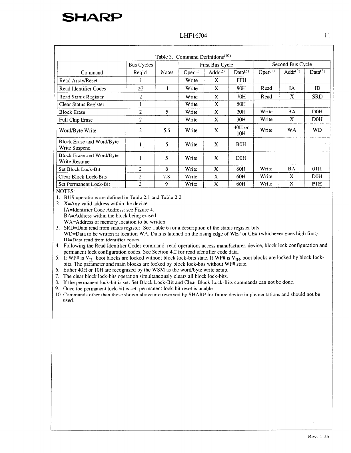
Table 3. Command Definition&to)
1 Block Erase I 2 1 5 1 Write 1 X 1 20H 1 Write 1 BA 1 DOH 1
1 Full Chio Erase
Word/Byte Write
Block Erase and Word/Byte
Write Suspend -.
Block Erase and Word/Byte
Write Resume
Set Block Lock-Bit
Clear Block Lock-Bits
Set Permanent Lock-Bit
NOTES:
1. BUS operations are defined in Table 2.1 and Table 2.2.
2. X=Any valid address within the device.
IA=Identifier Code Address: see Figure 4.
BA=Address within the block being erased.
WA=Address of memory location to be written.
3. SRD=Data read from status register. See Table 6 for a description of the status register bits.
WD=Data to be written at location WA. Data is latched on the rising edge of WE# or CE# (whichever goes high first).
ID=Data read from identifier codes.
4. Following the Read Identifier Codes command, read operations access manufacturer, device, block lock configuration and
permanent lock configuration codes. See Section 4.2 for read identifier code data.
5. If WP# is V,, boot blocks are locked without block lock-bits state. If WP# is V,,, boot blocks are locked by block lockbits. The parameter and main blocks are locked by block lock-bits without WP# state.
6. Either 4OH or 10H are recognized by the WSM as the word/byte write setup.
7. The clear block lock-bits operation simultaneously clears all block lock-bits.
8. If the permanent lock-bit is set, Set Block Lock-Bit and Clear Block Lock-Bits commands can not be done.
9. Once the permanent lock-bit is set. permanent lock-bit reset is unable.
10. Commands other than those shown above are reserved by SHARP for future device implementations and should
I
2 I
2
1 5 Write X BOH
1 5 Write X DOH
2 8 Write X 60H
2 7.8 Write X 60H Write X DOH
2 9 Write X 60H
56
I
Write
Write X
I
X
l
30H I Write ( X I DOH I
40H or
10H
Write WA WD
Write BA
Write
X FlH
OIH
not be
Rev. 1.25
LHF16504
12
4.1 Read Array Command
Upon initial device power-up and after exit from reset
mode, the device defaults to read array mode. This
aperation is also initiated by writing the Read Array
zomrnand. The device remains enabled for reads until
mother command is written. Once the internal WSM has
started a block erase. full chip erase. word/byte write or
.ock-bit configuration the device will not recognize the
Read Array command until the WSIM completes its
operation unless the WSM is suspended via an Erase
Suspend or Word/Byte Write Suspend command. The
iead Array command functions independently of the
Vccw
voltage and RP# can be Vt,.
L
1.2 Read Identifi& Codes Command
The identifier code operation is initiated by writing the
i
tead Identifier Codes command. Following the command
\
write. read cycles from addresses shown in Figure 4
r
etrieve the manufacturer. device, block lock configuration
a
tnd permanent lock configuration codes (see Table 4 for
i’
dentifier code values). To terminate the operation. write
a
another valid command. Like the Read Array command,
t
he Read Identifier Codes command functions
ndependently of the Vccw voltage and RP# can be V,,.
;
:ollowing the Read Identifier Codes command. the
f
ollowing information can be read:
Table 4. Identifier Codes
4.3 Read Status Register Command
The status register may be read to determine when a block
erase, full chip erase. word/byte write or lock-bil
configuration is complete and whether the operation
completed successfully. It may be read at any time by
writing the Read Status Register command. After writing
this command, all subsequent read operations output data
from the status register until another valid command is
written. The status register contents are latched on the
falling edge of OE# or CE#. whichever occurs. OE# or
CE# must toggle to V,, before further reads to update the
status register latch. The Read Status Register command
functions independently of the Vccw voltage. RP# can be
VI,.
4.4 Clear Status Register Command
Status register bits SRS. SR.4 SR.3 or SR.1 are set to
“1”s by the WSM and can only be reset by the Clear Status
Register command. These bits indicate various failure
conditions (see Table 6). By allowing system software to
reset these bits. several operations (such as cumulatively
erasing multiple blocks or writing several words/bytes in
sequence) may be performed. The status register may be
polled to determine if an error occurred during the
sequence.
To clear the status register, the Clear Status Register
command (50H) is written. It functions independently of
the applied Vccw
command is not functional during block erase or
word/byte write suspend modes.
Voltage. RP# can be V,,. This
Block Lock Configuration
*Block is Unlocked
*Block is Locked
*Reserved for Future Use
Permanent Lock Configuration
*Device is Unlocked
*Device is Locked
*Reserved for Future Use
IOTE:
BA selects the specific block lock configuration code
to be read. See Figure 4 for the device identifier code
memory map.
A-, don’t care in byte mode.
DQ, ,-DQ, outputs OOH in word mode.
DQI-7
Rev. 1.25
SHARP
LHF 16JO4
4.5 Block Erase Command
Erase is executed one block at a time and initiated by a
two-cycle command. A block erase setup is first written.
followed by an block erase confirm. This command
sequence requires appropriate sequencing and an address
within the block to be erased (erase changes all block data
to FFFFH/FFH). Block preconditioning. erase, and verify
are handled internally by the WSIM (invisible to the
system). After the two-cycle block erase sequence is
written. the device automatically outputs status register
data when read (see Figure 5). The CPU can detect block
erase completion by analyzing the output data of the
RY/BY# pin or status register bit SR.7.
When the block erase-is complete, status register bit SR.5
should be checked. If a block erase error is detected. the
status register should be cleared before system software
Ittempts corrective actions. The CUI remains in read
status register mode until a new command is issued.
I’his two-step command sequence of set-up followed by
:xecution ensures that block contents are not accidentally
:rased. An invalid Block Erase command sequence will
esult in both status register bits SR.4 and SR.5 being set
o “1”. Also, reliable block erasure can only occur when
dcc=2.7V-3.6V and VCCW=VC-wBl,,. In the absence of
his high voltage. block contents are protected against
:rasure. If block erase is attempted while VCCW<VCCWLK.
iR.3 and SR.5 will be set to “1”. Successful block erase
equires for boot blocks that WP# is V,, and the
,orresponding block lock-bit be cleared. In parameter and
nain blocks case, it must be cleared the corresponding
Ilock lock-bit. If block erase is attempted when the
xcepting above conditions. SR.1 and SR.5 will be set to
1 ‘I,
I.6 Full Chip Erase Command
his command followed by a confirm command erases all
f the unlocked blocks. A full chip erase setup (30H) is
lrst written, followed by a full chip erase confirm (DOH).
hfter a confirm command is written, device erases the all
nlocked blocks block by block. This command sequence
:quires appropriate sequencing. Block preconditioning,
rase and verify are handled internally by the WSM
nvisible to the system). After the two-cycle full chip
rase sequence is written, the device automatically outputs
atus register data when read (see Figure 6). The CPU can
etect full chip erase completion by analyzing the output
ata of the RY/BY# pin or status register bit SR.7.
ihen the full chip erase is complete. status register bit
R.5 should be checked. If erase error is detected, the
atus register should be cleared before system software
tempts corrective actions. The CUI remains in read
13
status register mode until a new command is issued. I
error is detected on a block during full chip erase
operation. WSM stops erasing. Full chip erase operatior
start from lower address block. finish the higher addres:
block. Full chip erase can not be suspended.
This two-step command sequence of set-up followed by
execution ensures that block contents are not accidentally
erased. An invalid Full Chip Erase command sequencr
will result in both status register bits SR.4 and SR.5 being
set to “1”. Also, reliable full chip erasure can only occur
when V,,=2.JV-3.6V and VCCW=VCCWHt,2. In thr
absence of this high voltage, block contents are protectec
against erasure. If full chip erase is attempted while
ccwlV,,,,, SR.3 and SR.5 will be set to “1”
V
Successful full chip erase requires for boot blocks thal
WP# is V,, and the corresponding block lock-bit be
cleared. In parameter and main blocks case, it must be
cleared the corresponding block lock-bit. If all blocks are
locked. SR.1 and SR.5 will be set to “1”.
4.7 Word/Byte Write Command
Word/Byte write is executed by a two-cycle command
sequence.
alternate 10H) is written. followed by a second write that
specifies the address and data (latched on the rising edge
of WE#). The WSiM then takes over, controlling the
word/byte write and write verify algorithms internally.
After the word/byte write sequence is written. the device
automatically outputs status register data when read (see
Figure 7). The CPU can detect the completion of the
word/byte write event by analyzing the RY/BY# pin or
status register bit SR.7.
When word/byte write is complete, status register bit SR.4
should be checked. If word/byte write error is detected. the
status register should be cleared. The internal WSM verify
only detects errors for “1”s that do not successfully write
to “0”s. The CUI remains in read status register mode until
it receives another command.
Reliable word/byte writes can only occur when
V,,=2.7V-3.6V and VCCw=VC-wHIR. In the absence of
this high voltage. memory contents are protected against
word/byte writes. If word/byte write is attempted while
V CCwIVCCLVLK. status register bits SR.3 and SR.4 will be
set to “1”. Successful word/byte write requires for boot
blocks that WP# is Vt, and the corresponding block lockbit be cleared. In parameter and main blocks case. it must
be cleared the corresponding block lock-bit. If word/byte
write is attempted when the excepting above conditions,
SR. 1 and SR.4 will be set to “1”.
Word/Byte write setup (standard 40H
OI
Rev. 1.25
 Loading...