

Page 1
TopPage
LC-32M400M-BK/WH/RD
SERVICE MANUAL
No. S51Q1LC32M40M
LCD COLOUR TELEVISION
LC-32M400M-BK
LC-32M400M-WH
MODELS
In the interests of user safety (required by safety regulations in some countries) the set should be restored to its
original condition and only parts identical to those specified should be used.
LC-32M400M-RD
CONTENTS
SAFETY PRECAUTION
IMPORTANT SERVICE SAFETY PRE-
CAUTION ............................................................i
PRECAUTIONS FOR USING LEAD-FREE
SOLDER ............................................................ ii
OUTLINE
MAJOR SERVICE PARTS ................................ iii
CHAPTER 1. SPECIFICATIONS
[1] SPECIFICATIONS ......................................... 1-1
CHAPTER 2. OPERATION MANUAL
[1] OPERATION MANUAL .................................. 2-1
CHAPTER 3. DIMENSIONS
[1] DIMENSIONS ................................................ 3-1
CHAPTER 4. REMOVING OF MAJOR PARTS
[1] REMOVING OF MAJOR PARTS ................... 4-1
CHAPTER 5. ADJUSTMENT
[1] ADJUSTMENT PROCEDURE ....................... 5-1
[2] USB Clone (Smart Loader) ............................ 5-6
[3] PUBLIC MODE SETTING PROCEDURE........ 5-7
CHAPTER 6. TROUBLESHOOTING TABLE
[1] TROUBLESHOOTING TABLE ......................6-1
CHAPTER 7. OVERALL WIRING/BLOCK DIAGRAM
[1] OVERALL WIRING DIAGRAM ......................7-1
[2] SYSTEM BLOCK DIAGRAM .........................7-2
CHAPTER 8. PRINTED WIRING BOARD ASSEMBLIES
[1] MAIN Unit ...................................................... 8-1
[2] IR OPC Unit ...................................................8-4
[3] TERMINAL Unit ............................................. 8-5
CHAPTER 9. SCHEMATIC DIAGRAM
[1] DESCRIPTION OF SCHEMATIC DIA-
GRAM............................................................9-1
[2] MAIN Unit ...................................................... 9-2
[3] IR OPC Unit .................................................9-13
[4] TERMINAL Unit ........................................... 9-14
Parts Guide
Parts marked with " " are important for maintaining the safety of the set. Be sure to replace these parts with specified ones for maintaining the
safety and performance of the set.
This document has been published to be used for
after sales service only.
The contents are subject to change without notice.
Page 2
LC-32M400M-BK/WH/RD
LC32M400MBK
SAFETY PRECAUTION
Service Manual
IMPORTANT SERVICE SAFETY PRECAUTION
Service work should be performed only by qualified service technicians who are thoroughly familiar with all safety checks and the
servicing guidelines which follow:
WARNING
1. For continued safety, no modification of any circuit should be
attempted.
2. Disconnect AC power before servicing.
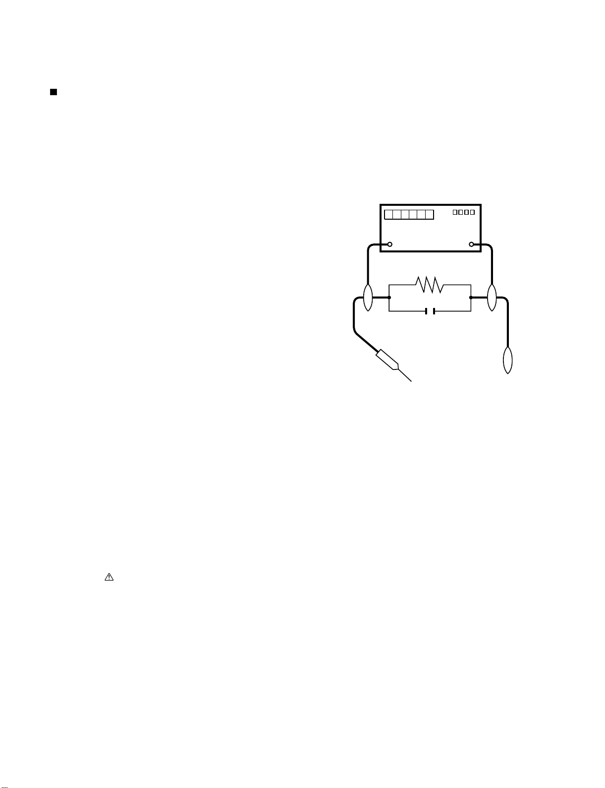
BEFORE RETURNING THE RECEIVER (Fire &
All checks must be repeated with the AC cord plug connection
reversed. (If necessary, a nonpolarized adaptor plug must be used
only for the purpose of completing these checks.)
Any reading of 0.74 Vrms (this corresponds to 0.5 mA rms AC.) or
more is excessive and indicates a potential shock hazard which
must be corrected before returning the monitor to the owner.
Shock Hazard)
Before returning the receiver to the user, perform the following
safety checks:
3. Inspect all lead dress to make certain that leads are not pinched,
and check that hardware is not lodged between the chassis and
other metal parts in the receiver.
4. Inspect all protective devices such as non-metallic control knobs,
insulation materials, cabinet backs, adjustment and compartment
covers or shields, isolation resistor-capacitor networks, mechanical
insulators, etc.
5. To be sure that no shock hazard exists, check for leakage current in
the following manner.
• Plug the AC cord directly into a 110-240 volt AC outlet.
• Using two clip leads, connect a 1.5k ohm, 10 watt resistor paralleled by a 0.15µF capacitor in series with all exposed metal cabinet
parts and a known earth ground, such as electrical conduit or electrical ground connected to an earth ground.
• Use an AC voltmeter having with 5000 ohm per volt, or higher, sensitivity or measure the AC voltage drop across the resistor.
• Connect the resistor connection to all exposed metal parts having a
return to the chassis (antenna, metal cabinet, screw heads, knobs
and control shafts, escutcheon, etc.) and measure the AC voltage
drop across the resistor.
///////////////////////////////////////////////////////////////////////////////////////////////////////////////////////////////////////////////////////////////////////////////////////////////////////////////////////////////////////////
TO EXPOSED
METAL PARTS
DVM
AC SCALE
1.5k ohm
10W
0.15µF
TEST PROBE
CONNECT TO
KNOWN EARTH
GROUND
SAFETY NOTICE
Many electrical and mechanical parts in LCD colour television have
special safety-related characteristics.
These characteristics are often not evident from visual inspection, nor
can protection afforded by them be necessarily increased by using
replacement components rated for higher voltage, wattage, etc.
Replacement parts which have these special safety characteristics are
identified in this manual; electrical components having such features
are identified by " " and shaded areas in the Replacement Parts List
and Schematic Diagrams.
///////////////////////////////////////////////////////////////////////////////////////////////////////////////////////////////////////////////////////////////////////////////////////////////////////////////////////////////////////////
For continued protection, replacement parts must be identical to those
used in the original circuit.
The use of a substitute replacement parts which do not have the same
safety characteristics as the factory recommended replacement parts
shown in this service manual, may create shock, fire or other hazards.
i
Page 3
LC-32M400M-BK/WH/RD
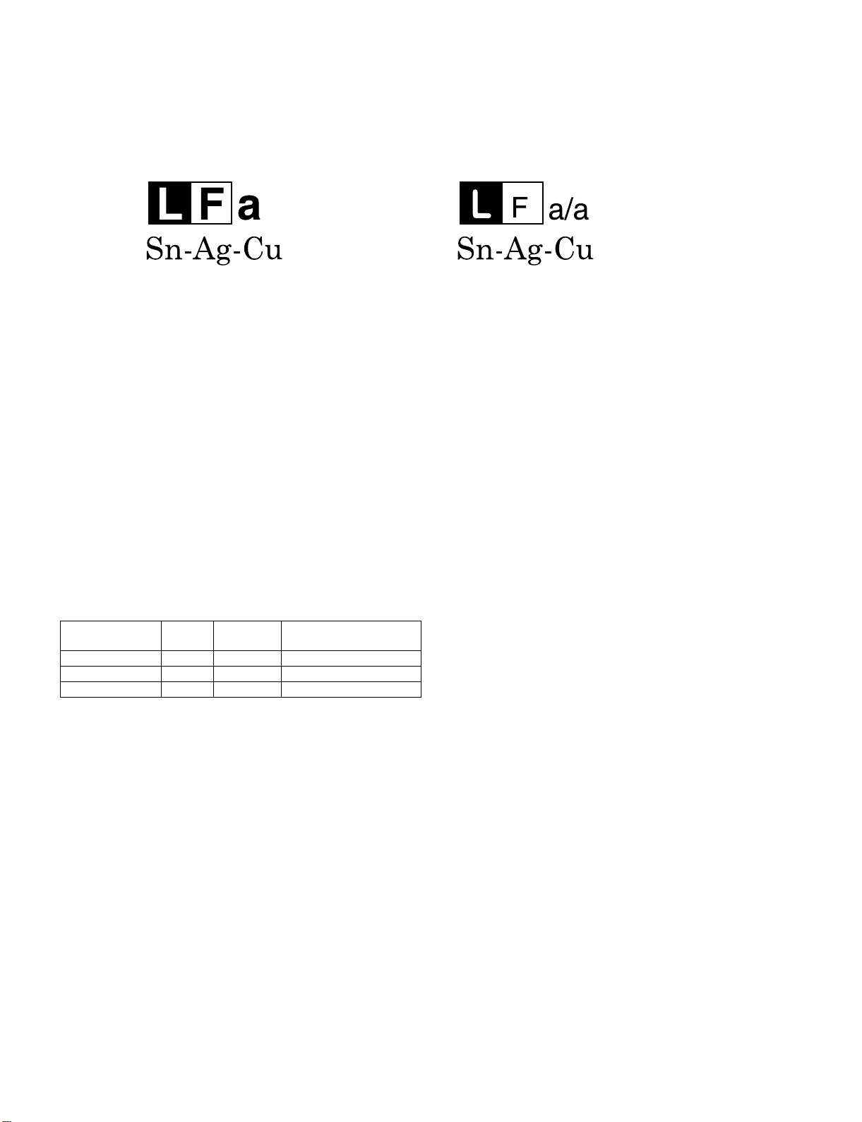
PRECAUTIONS FOR USING LEAD-FREE SOLDER
Employing lead-free solder
• “PWBs” of this model employs lead-free solder. The LF symbol indicates lead-free solder, and is attached on the PWBs and service manuals. The
alphabetical character following LF shows the type of lead-free solder.
Example:
Indicates lead-free solder of tin, silver and copper. Indicates lead-free solder of tin, silver and copper.
Using lead-free wire solder
• When fixing the PWB soldered with the lead-free solder, apply lead-free wire solder. Repairing with conventional lead wire solder may cause damage or accident due to cracks.
As the melting point of lead-free solder (Sn-Ag-Cu) is higher than the lead wire solder by 40 °C, we recommend you to use a dedicated soldering
bit, if you are not familiar with how to obtain lead-free wire solder or soldering bit, contact our service station or service branch in your area.
Soldering
• As the melting point of lead-free solder (Sn-Ag-Cu) is about 220 °C which is higher than the conventional lead solder by 40 °C, and as it has poor
solder wettability, you may be apt to keep the soldering bit in contact with the PWB for extended period of time. However, Since the land may be
peeled off or the maximum heat-resistance temperature of parts may be exceeded, remove the bit from the PWB as soon as you confirm the
steady soldering condition.
Lead-free solder contains more tin, and the end of the soldering bit may be easily corroded. Make sure to turn on and off the power of the bit as
required.
If a different type of solder stays on the tip of the soldering bit, it is alloyed with lead-free solder. Clean the bit after every use of it.
When the tip of the soldering bit is blackened during use, file it with steel wool or fine sandpaper.
• Be careful when replacing parts with polarity indication on the PWB silk.
Lead-free wire solder for servicing
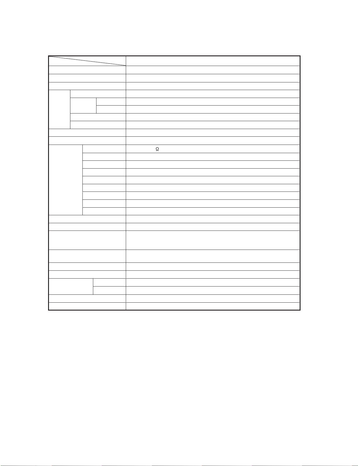
PARTS CODE
ZHNDAi123250E BL J φ0.3mm 250g (1roll)
ZHNDAi126500E BK J φ0.6mm 500g (1roll)
ZHNDAi12801KE BM J φ1.0mm 1kg (1roll)
PRICE
RANK
PART
DELIVERY
DESCRIPTION
ii
Page 4
LC-32M400M-BK/WH/RD
LC32M400MBK
OUTLINE
Service Manual
MAJOR SERVICE PARTS
PWB UNIT
Ref No. Part No. Description
N DKEYMF878FM01 MAIN Unit (Except for Philippines)
N DKEYMF878FM02 MAIN Unit (for Philippines)
N DUNTKF879WE01 IR/OPC Unit
N DUNTKF885FM01 TERMINAL Unit
N RDENCA438WJPZ POWER Unit
N RUNTKA860WJPZ INVERTER Unit
OTHER UNIT
Ref No. Part No. Description
N R1LK315T3LW7AW 32” LCD Panel Module
IC FOR EXCLUSIVE USE OF THE SERVICE
Ref No. Part No. Description Q'ty
IC508 RH-iXD169WJQZS IC, PC EDID 1
IC1501 RH-iXD170WJQZS IC, HDMI 1 EDID 1
IC1502 RH-iXD189WJQZS IC, HDMI 3 EDID 1
IC1503 RH-iXD188WJQZS IC, HDMI 2 EDID 1
SERVICE JIGS
Ref No. Part No. Description Q’ty
N QCNW-M159WJPZ Connecting Cord, TERMINAL-LCD Control (RA) 1
N QCNW-M160WJPZ Connecting Cord, MAIN-POWER (PI) 1
N QCNW-M161WJPZ Connecting Cord, MAIN-Speaker (SP) 1
N QCNW-M162WJPZ Connecting Cord, MAIN-LCD Control (LW) 1
N QCNW-M165WJPZ Connecting Cord, POWER-INVERTER (VA/VB) 2
iii
Page 5
LC32M400MBK
CHAPTER 1. SPECIFICATIONS
[1] SPECIFICATIONS
LC-32M400M-BK/WH/RD
Service Manual
Item
LCD panel
Resolution
Video Colour System PAL/SECAM/NTSC 3.58/NTSC 4.43/PAL 60
TV
Function
Viewing angles H : 176º V : 176º
Audio amplifier/Speakers
Terminals Antenna input
USB device/File system USB Memory / FAT/FAT32
Photo file format JPEG (.jpg) (DCF2.0 compliant). Progressive format jpeg files are not supported.
Music file format
(Files may not be playable
depending on the bitrate.)
OSD language English/Simplied Chinese/Arabic/French/Portuguese/Russian/Persian/Thai/
Power Requirement AC 110—240 V, 50/60 Hz
Power Consumption 102 W (0.8 W Standby)
Dimensions
Weight
Operating Temperature 0°C — 40°C
• As a part of policy of continuous improvement, SHARP reserves the right to make design and specification changes for
product improvement without prior notice. The performance specification figures indicated are nominal values of production
units. There may be some deviations from these values in individual units.
TV-Standard PAL: B/G, D/K, I SECAM: B/G, D/K, K/K
Receiving
Channel
TV-Tuning System Auto Preset 99 ch
STEREO/BILINGUAL NICAM: B/G, I, D/K A2 stereo: B/G
INPUT 1 HDMI (HDMI input), AUDIO in (
INPUT 2/INPUT 3 HDMI (HDMI input) / HDMI (HDMI input)
INPUT 4 S-VIDEO in, VIDEO in, AUDIO in
INPUT5 VIDEOin,AUDIOin
INPUT6 AUDIO in, COMPONENT in
INPUT 7 (PC input) 15 pin mini D-sub, AUDIO in (common use with INPUT 1) (
AUDIO OUT AUDIO out
RS-232C 9 pin D-sub male connector
Model
VHF/UHF 44.25—863.25 MHz
CATV
without stand
with stand
LC-32M400M
31.5" (800 mm) Advanced Super View & BLACK TFT LCD
1,049,088 pixels (1366 x 768)
1
NTSC: M
S1—S41ch (including Hyperband)
5Wx2/5x9cm 2pcs
UHF/VHF 75
MP3(.mp3) Bitrate:32k,40k,48k,56k,64k,80k,96k,112k,128k,160k,
192 k, 224 k, 256 k, 320 kbps
Sampling frequency: 32 k, 44.1 k, 48 kHz
Vietnamese/Indonesian
792 (W) x 540 (H) x 113 (D) mm
792 (W) x 576 (H) x 242 (D) mm
8.5 kg (without stand) / 9.2 kg (with stand)
DIN type
Ø
3.5 mm jack)
Ø
3.5 mm jack)
1 – 1
Page 6
LC-32M400M-BK/WH/RD
LC32M400MBK
CHAPTER 2. OPERATION MANUAL
[1] OPERATION MANUAL
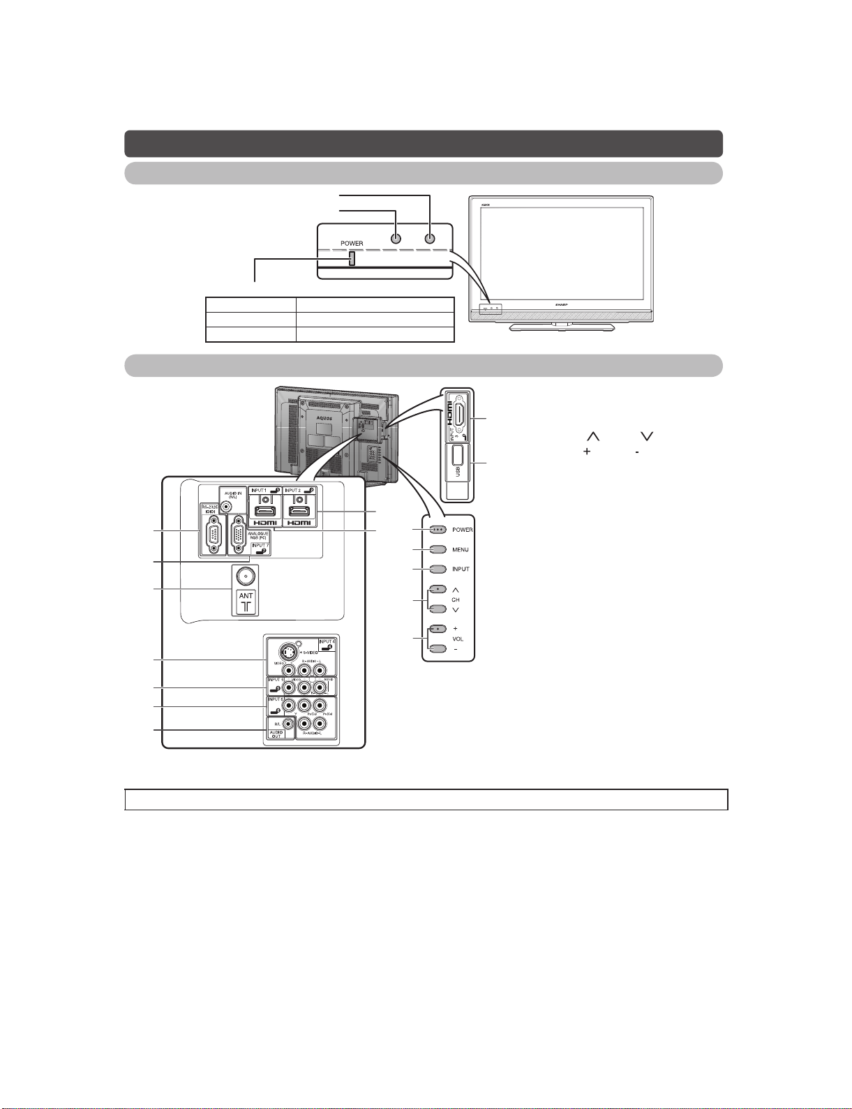
Part names
TV (Front)
Remote control sensor
OPC sensor
POWER indicator
Light off Power off
Lighted (Red) The TV is in standby mode.
Lighted (Green) The TV is on.
TV (Rear)
13
6
7
8
9
14
Service Manual
1
2
3
4
5
1POWER(On/Off) button
2MENUbutton
15
3INPUTbutton
4 Channel up ( )/down ( ) buttons
5 Volume up ( )/down ( ) buttons
16
6 RS-232C terminal
7INPUT 7 (PC) terminals*
8 Antenna input terminal
9 INPUT 4 terminals
10 INPUT 5 terminals
11 INPUT 6 terminals
12 AUDIO OUT terminal
13 INPUT 2 (HDMI) terminal
14 INPUT 1 (HDMI) terminal*
15 INPUT 3 (HDMI) terminal
16 USB terminal
10
11
12
* The INPUT 1 and INPUT 7 terminals can both use the same audio input terminal. However, the proper item must be
selected in the “PC Audio Select” menu.
• The illustrations in this operation manual are for explanation purposes and may vary slightly from the actual operations.
2 – 1
Page 7
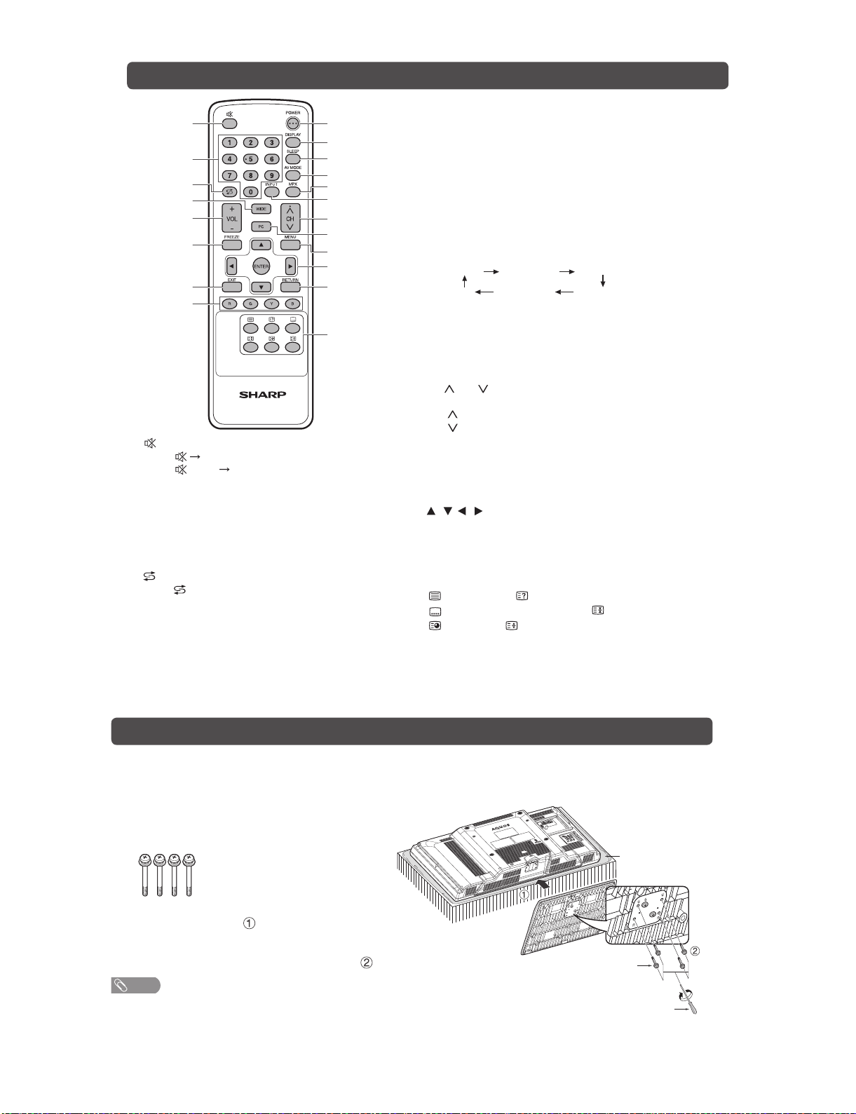
Remote control unit
1
2
3
4
5
6
7
8
1 (Mute)
Press
Press again Restores sound.
Mute will be cancelled after 30 minutes. However,
the TV will not suddenly output loud sound as the
volume level will be set to 0 automatically. Increase
the volume level by pressing VOL +.
20–9
Set the channel.
TELETEXT mode: Set the page.
3 (Flashback)
Press to return to the previous selected channel
or external input mode.
4 WIDE
Change the wide image mode.
5VOL+/VOL
Set the volume.
(VOL+) Increase the volume.
(VOL-) Decrease the volume.
Mutes sound.
-
9
10
11
12
13
14
15
16
17
18
19
20
LC-32M400M-BK/WH/RD
6 FREEZE
Freeze a motion picture on the screen.
7EXIT
Return to the default screen.
8 Colour (Red/Green/Yellow/Blue)
TELETEXT mode: Select a page.
9 POWER (STANDBY/ON)
To switch the power on and off.
10 DISPLAY
Display the channel or input information.
11 SLEEP
Set the Sleep timer.
0 hr. 30 min. 1 hr. 00 min.
Off
2 hr. 30 min.
12 AV MODE
Select an audio and video setting.
13 MPX
Select the sound multiplex mode.
14 INPUT (INPUT SOURCE)
Select an input source.
15 CH /C H
TV input mode: Select the channel.
(CH ) Increase the channel number.
(CH ) Decrease the channel number.
TELETEXT mode: Select the page.
16 PC
Directly select the PC terminal.
17 MENU
Display the menu screen.
18 / / / (Cursor)
Select a desired item on the setting screen.
ENTER
Execute a command.
19 RETURN
MENU mode: Return to the previous menu screen.
20 (TELETEXT), (Reveal hidden for TELETEXT),
(SUBTITLE for TELETEXT), (Hold),
(Subpage), (Top/Bottom/Full)
Use for TELETEXT mode.
1 hr. 30 min.
2 hr. 00 min.
Attaching the stand
• Before attaching (or detaching) the stand, unplug the AC cord from the AC outlet.
• Before performing work spread cushioning over the base area to lay the TV on. This will prevent it from
being damaged.
Confirm the screws supplied with the TV.
1
Screws (x 4)
(usedinstep3)
Insert the stand base to the stand post on the
2
bottom of the TV. ( )
Insert and tighten the 4 screws into the 4
3
holes on the bottom of the stand base.( )
NOTE
• To detach the stand, perform the steps in reverse
order.
2 – 2
Soft cushion
Screw
Screw driver
Page 8
LC-32M400M-BK/WH/RD
PC Control of the TV
•
When a programme is set, the TV can be controlled from the PC using the RS-232C terminal.
The input signal (PC/video) can be selected, the volume can be adjusted and various other
adjustments and settings can be made, enabling automatic programmed playing.
•
Attach an RS-232C cable cross-type (commercially available) to the Din/D-sub RS-232C for the
connections.
NOTE
•
This operation system should be used by a person who is accustomed to using PCs.
Communication conditions
Set the RS-232C communications settings on the PC to match the communications conditions of
the TV. The communications settings of the TV are as follows:
Baud rate: 9,600 bps
Data length: 8bits
Parity bit: None
Stop bit: 1bit
Flow control: None
Communication procedure
Send the control commands from the PC via the RS-232C connector.
The TV operates according to the received command and sends a response message to the PC.
Do not send multiple commands at the same time. Wait until the PC receives the OK response before
sending the next command.
Command format
Eight ASCII codeseCR
C1 C2 C3 C4 P1 P2 P3 P4
Command 4-digits Parameter 4-digits Return code
Command 4-digits: Command. The text of four
characters.
Parameter 4-digits: Parameter 0 - 9, space, ?
Parameter
Input the parameter values, aligning left, and fill with space(s) for the remainder. (Be sure that four
values are input for the parameter.)
When the input parameter is not correct, "ERR" returns. (Refer to "Response code format".)
0
0009
a30
Response code format
Problem response (communication error or
Normal response
incorrect command)
OK ERR
Return code (0DH)
Return code (0DH)
2 – 3
Page 9
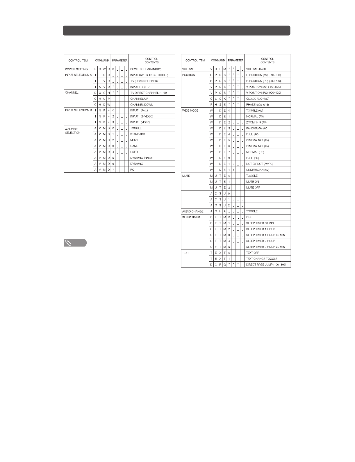
RS-232C commands list
Commands
•
Commands not indicated here are not guaranteed to operate.
4
4
4
LC-32M400M-BK/WH/RD
NOTE
•
If an underbar (_) appears in the parameter column,
enter a space.
•
If an asterisk (*) appears, enter a value in the range
indicated in brackets under CONTROL CONTENTS.
SURROUND TOGGLESURROUND
SURROUND ON
SURROUND OFF
2 – 4
Page 10
LC-32M400M-BK/WH/RD
LC32M400MBK
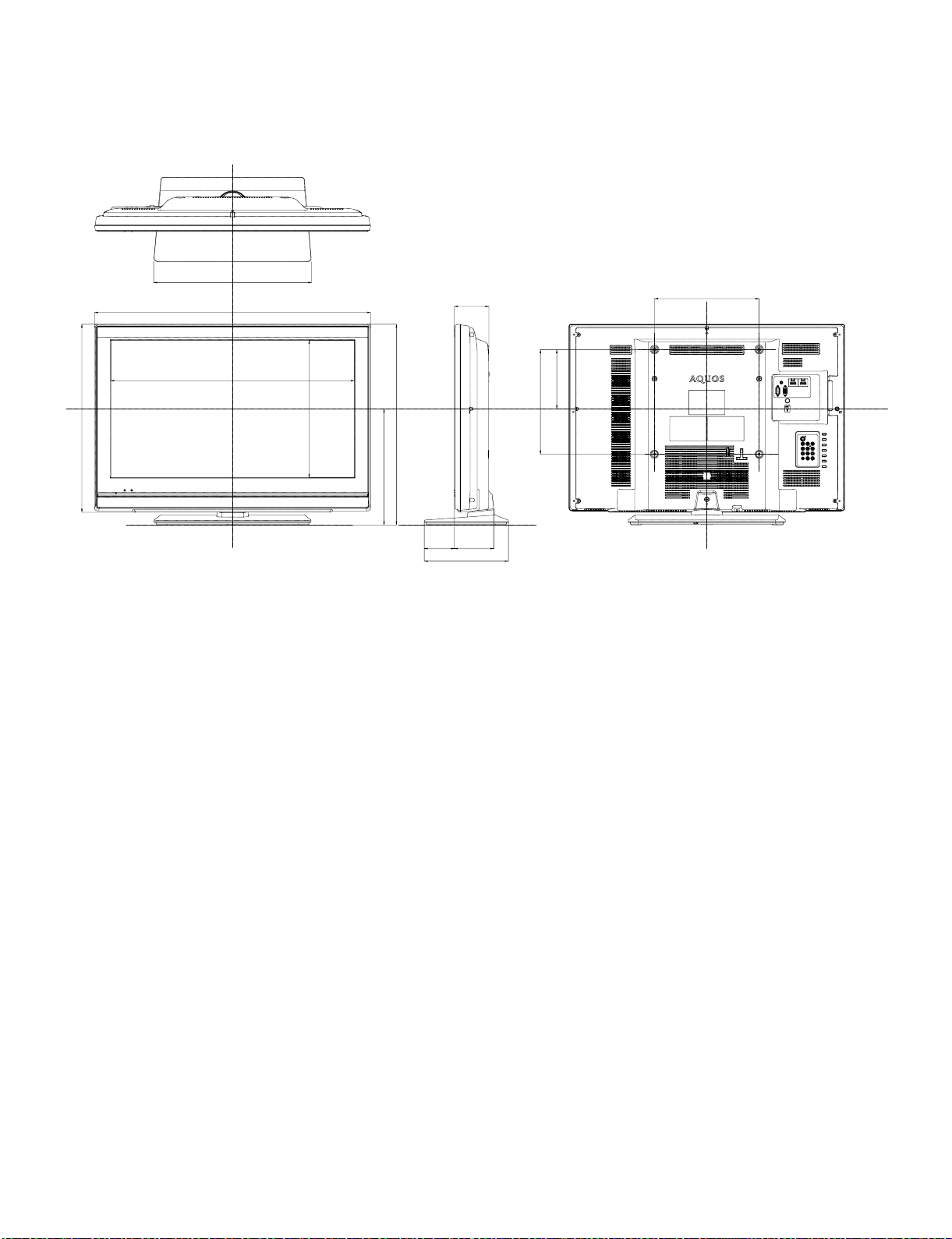
CHAPTER 3. DIMENSIONS
[1] DIMENSIONS
453
792.2
Service Manual
99.2
Unit: mm
300
539.5
699.2
393.8
333
575.9
86.3
170
300
113.3
241.6
3 – 1
Page 11
LC32M400MBK
CHAPTER 4. REMOVING OF MAJOR PARTS
Service Manual
[1] REMOVING OF MAJOR PARTS
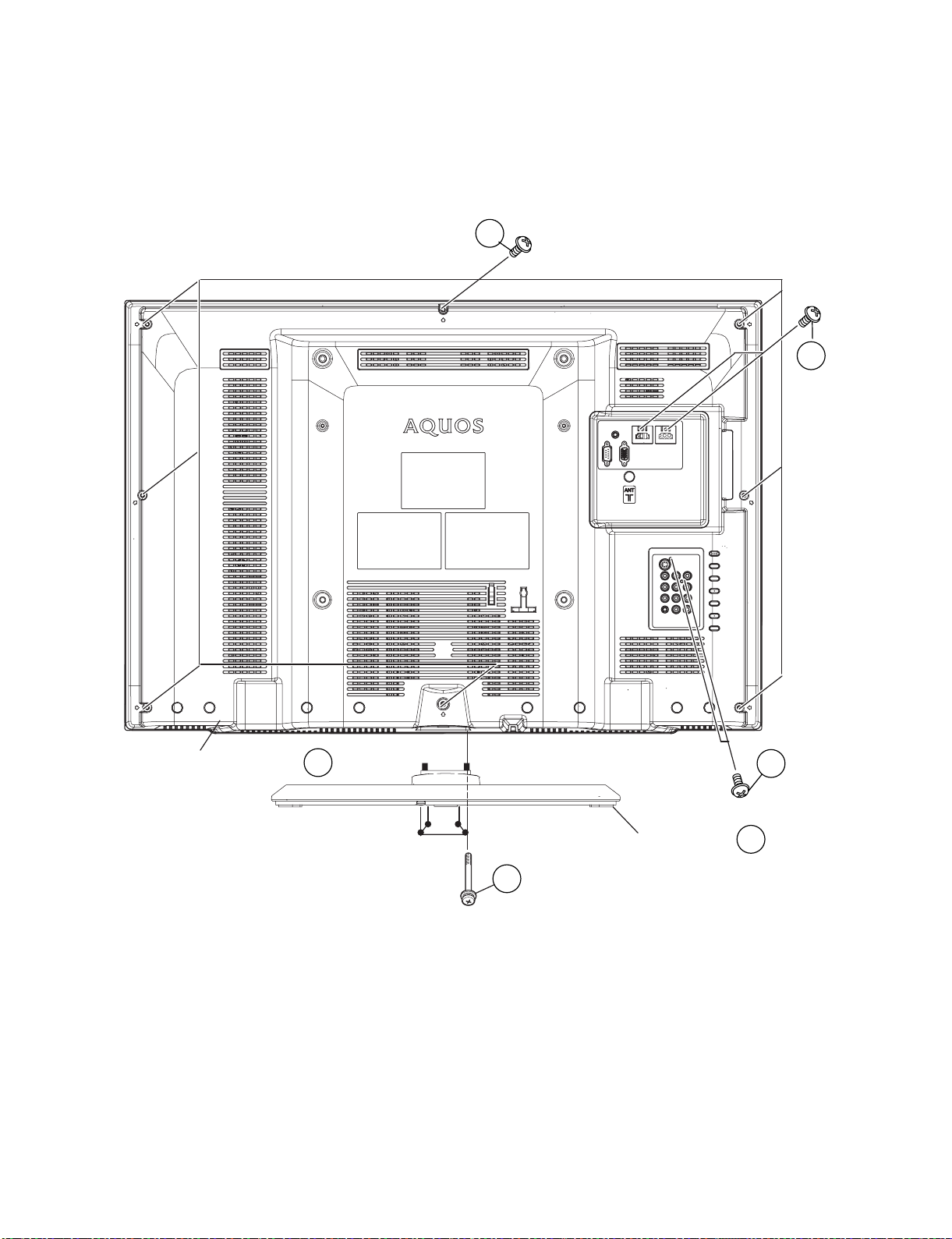
1. Removing of the Stand Unit and Rear Cabinet
1. Remove the 4 lock screws [1] and detach the Stand Unit [2].
2. Remove the 2 lock screws [3], 2 lock screw [4], 8 lock screw [5] and detach the Rear Cabinet Ass’y [6].
5
LC-32M400M-BK/WH/RD
4
Rear Cabinet Ass'y
6
Stand Unit
3
2
1
4 – 1
Page 12
LC-32M400M-BK/WH/RD
2. Disconnect the connectors
1. Disconnect the connectors from the MAIN Unit, IR/OPC Unit, POWER, Unit, TERMINAL Unit, INVERTER Unit and LCD Panel Module [1].
LCD Panel Module
VA/VB
1
POWER Unit
SP
LVDS
VA/VB
MAIN Unit
P0
LVDS
1
MA MB
MA MB
1
RA
SP
RA
PW
1
SP
AC
INVERTER Unit
IR/OPC Unit
4 – 2
Page 13
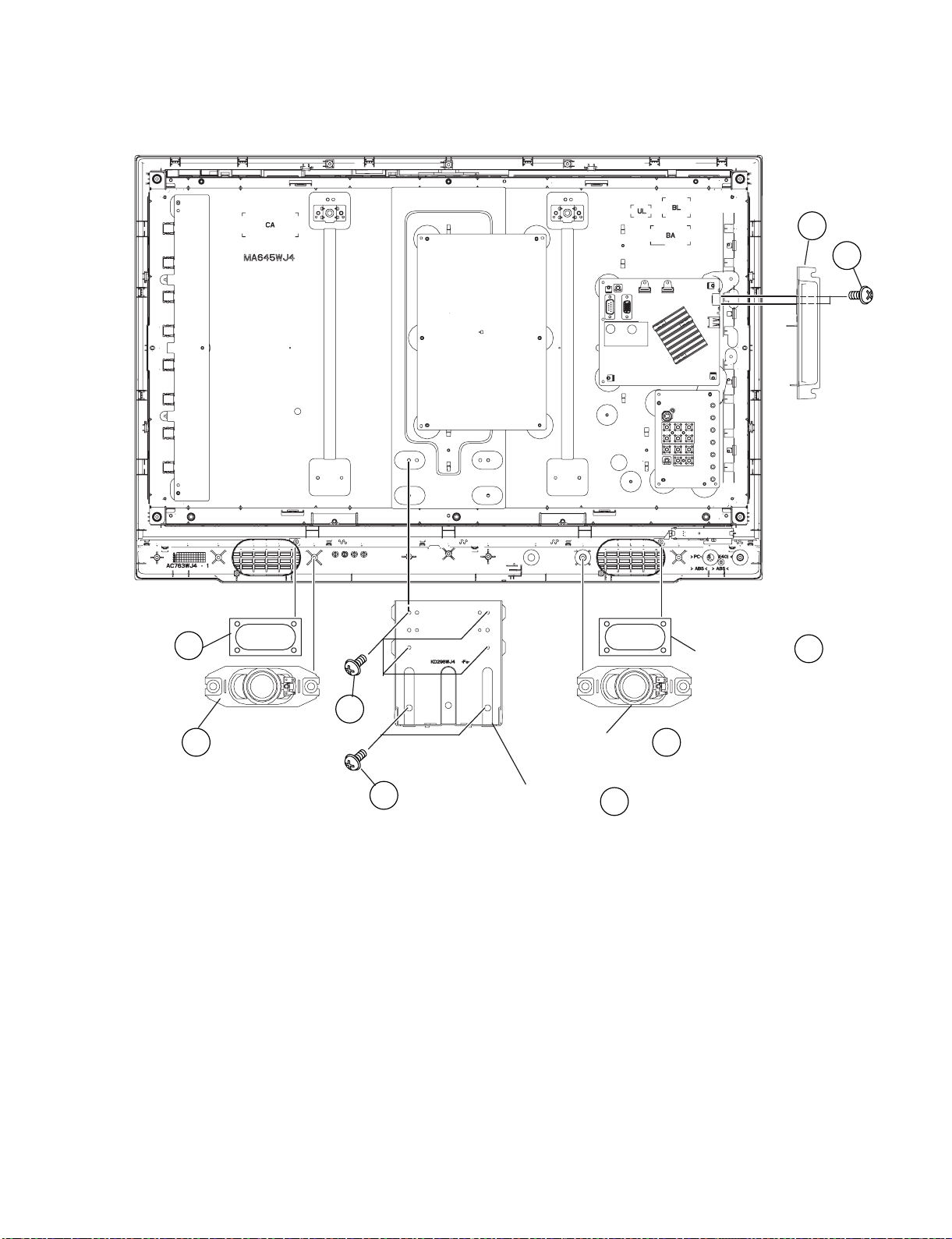
3. Removing of the Side AV Cover Ass’y, Speaker-L/R and Bottom Bracket
1. Remove the 2 lock screws [1], and detach the Side AV Cover Ass’y [2].
2. Remove the 2 lock screws [3], 4 lock screws [4] and detach the Bottom Bracket [5].
3. Detach the Speaker L/R [6] and the Molt Plane [7].
LC-32M400M-BK/WH/RD
Side AV
Cover Ass'y
2
1
Molt Plane
Speaker-L
7
Molt Plane
7
4
6
3
Bottom Bracket
Speaker-R
5
6
4 – 3
Page 14
LC-32M400M-BK/WH/RD
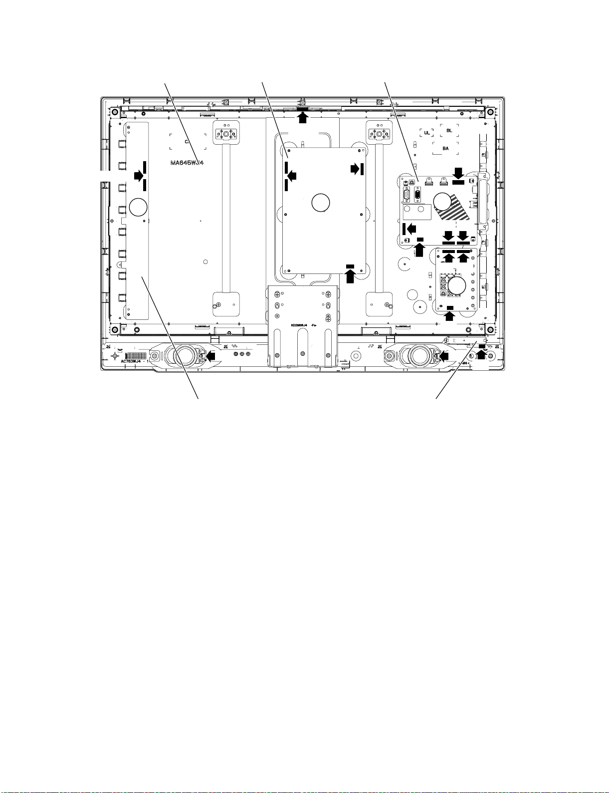
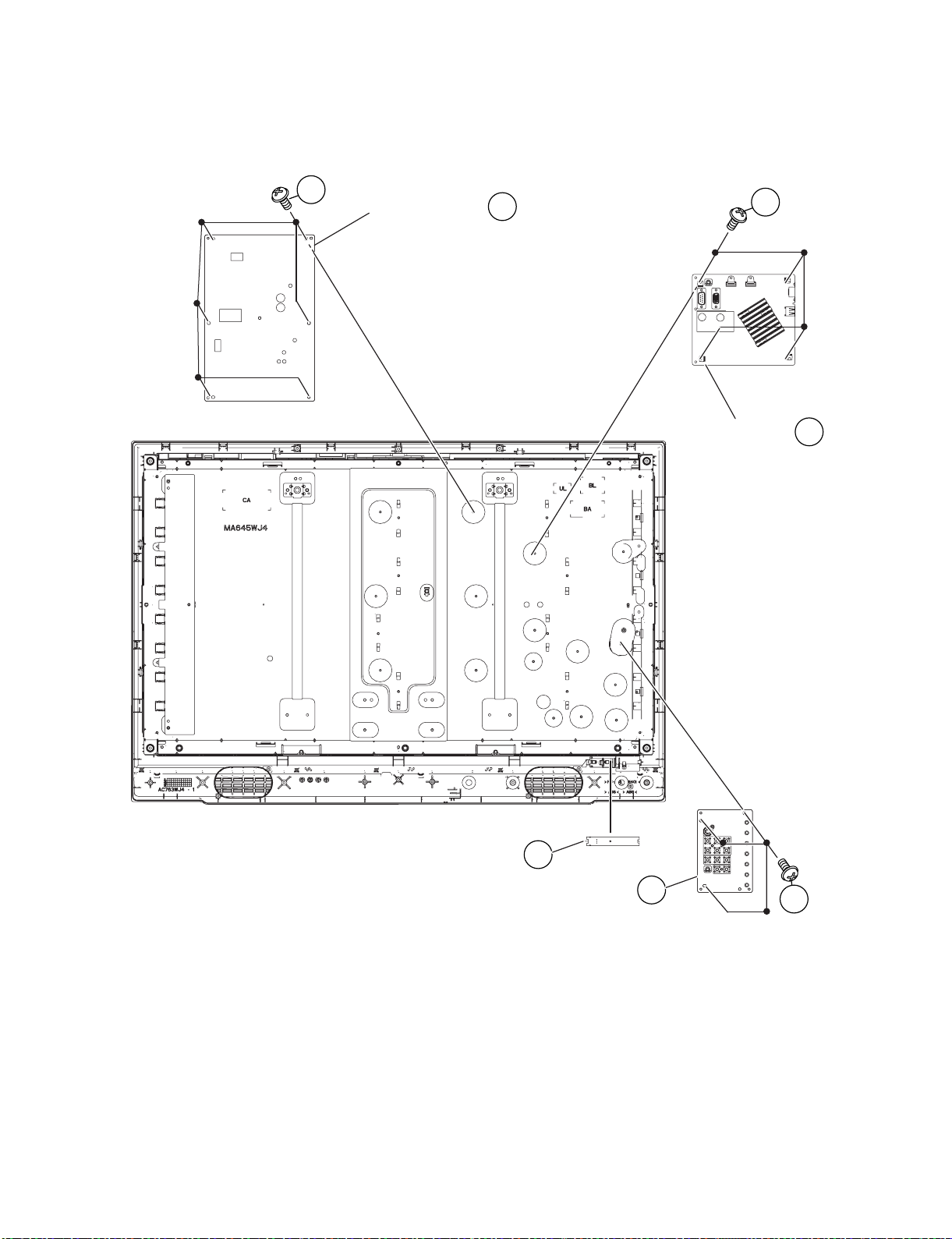
4. Removing of the PWB Units
1. Detach the IR/OPC Unit [1].
2. Remove the 4 lock screws [2] and detach the TERMINAL Unit [3].
3. Remove the 4 lock screws [4] and detach the MAIN Unit [5].
4. Remove the 6 lock screws [6] and detach the POWER Unit [7].
6
POWER Unit
7
MAIN Unit
4
5
IR OPC Unit
TERMINAL Unit
4 – 4
1
3
2
Page 15
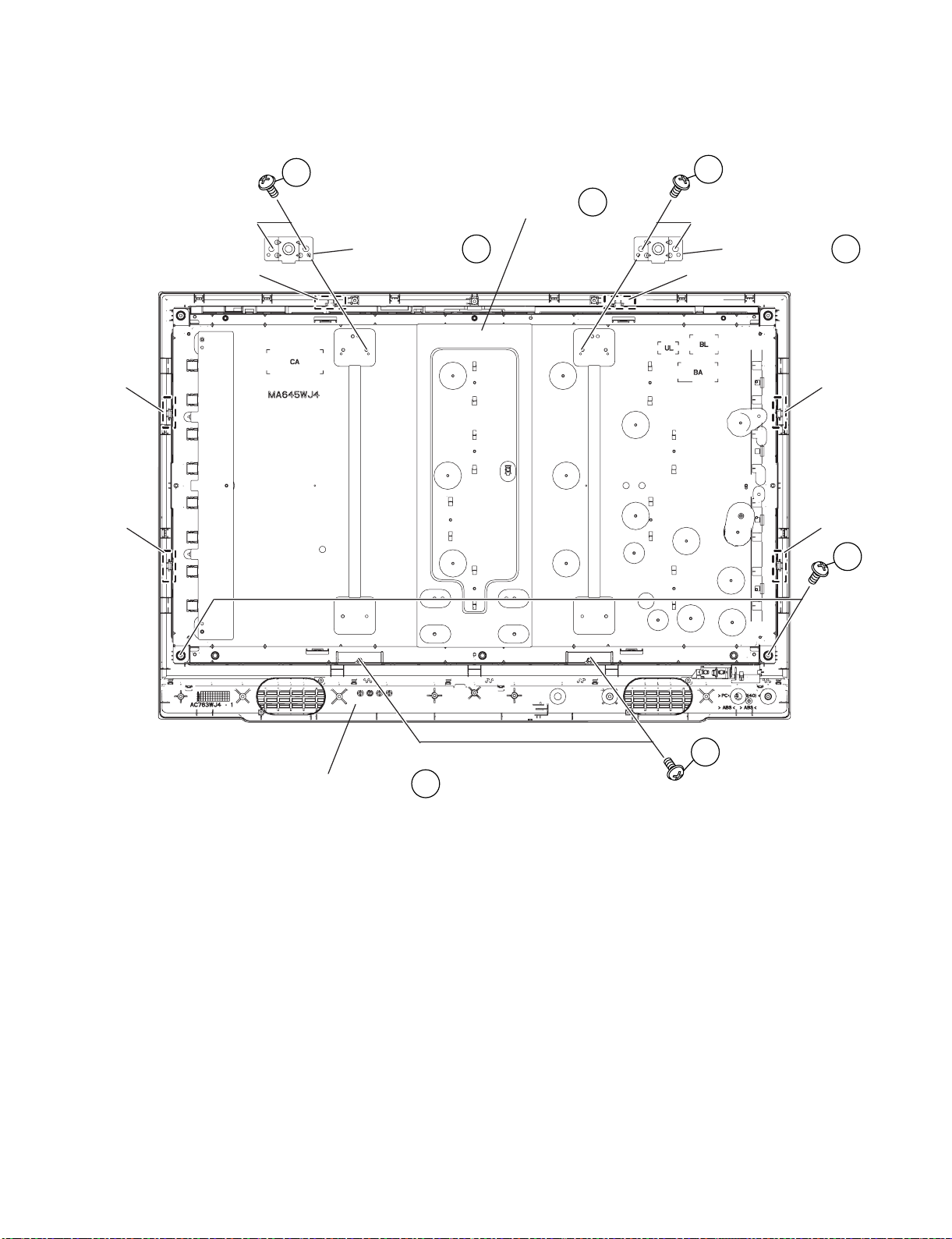
5. Removing of the LCD Panel Module
1. Remove the 4 lock screws [1] and detach VESA Angle [2].
2. Remove the 2 lock screws [3], 2 lock screws [4].
3. Detach the 6 pieces claws and detach the LCD Panel Module [5] from the Front Cabinet [6].
LC-32M400M-BK/WH/RD
Claw
Claw
Claw
1
LCD Panel Module
VESA Angle
2
5
1
VESA Angle
2
Claw
Claw
Claw
4
Front Cabinet Ass'y
3
6
4 – 5
Page 16
LC-32M400M-BK/WH/RD
LC32M400MBK
CHAPTER 5. ADJUSTMENT
Service Manual
[1] ADJUSTMENT PROCEDURE
1. Entering and cancel the adjustment process mode
1) While holding down the TV/VIDEO and Volume DOWN keys at the same time, plug in the AC cord to turn on the power. (“K” standing for inspection process mode is displayed on the upper left position of the screen.)
2) Press the Channel DOWN and Volume DOWN keys at the same time. (The adjustment process mode screen appears.)
3) To cancel it, turn off the power using the Power switch or remote control.
2. Remote controller key operation and description of display in adjustment process mode.
1. key operation
Remote controller key Main unit key Function
CH ( / )
VOL (+ / –) VOL (+ / –) Changing volume (UP/DOWN)
Cursor ( / )
Cursor ( / )
TV/VIDEO button on remote
controller
ENTER —————— ——————
* Input mode is switched automatically when relevant adjustment is started so far as the necessary input signal is available.
CH ( / )
—————— Turning a page (PREVIOUS/NEXT)
—————— Changing a selected line setting (+10/-10)
TV/VIDEO button Input source switching (toggle switching)
Changing channel (UP/DOWN)
(T V-DAV-1/ SAV-1 → AV- 2 → COMPONENT → HDMI → PC)
3. Software upgrading. (Method D)
1) Plug off the LCD TV.
2) Insert the USB device to the USB terminal at the LCD TV.
(Make sure that the latest software is installed in the USB device.)
3) Hold the LCD TV power key and plug on the LCD TV.
4) LCD TV is on and detecting the USB device.
USB device found
5) A few seconds later, the software upgrading will start automatically.
Do not power off
Chip Programming
>>>>>>>>
5 – 1
Page 17
6) Let the process running & entering verification.
Verifying
Verified
7) Software is successfully installed when the following appears at the end of the process.
LC-32M400M-BK/WH/RD
Please re-boot the system
Update Finished
8) Plug off the LCD TV and plug ON again as usual.
9) LCD TV is running with the latest software.
4. Signal adjustment
4.1. Signal check
Confirmation of signal from generator (setting to spec level)
• PAL Composite signal : 0.7Vp-p ± 0.02Vp-p (Pedestal to white level)
• 15K Component signal (50Hz) : Y level:
Pb, Pr level:
• 33K component signal : Y level:
Pb, Pr level:
4.1.1 PROCESS MODE
Adjustment item Adjustment conditions Adjustment procedure
1 Adjustment mode 1) Press the test key at the test remote control.
0.7Vp-p ± 0.02Vp-p (Pedestal to white level)
0.7Vp-p ± 0.02Vp-p
0.7Vp-p ± 0.02Vp-p (Pedestal to white level)
0.7Vp-p ± 0.02Vp-Com
5 – 2
Page 18
LC-32M400M-BK/WH/RD
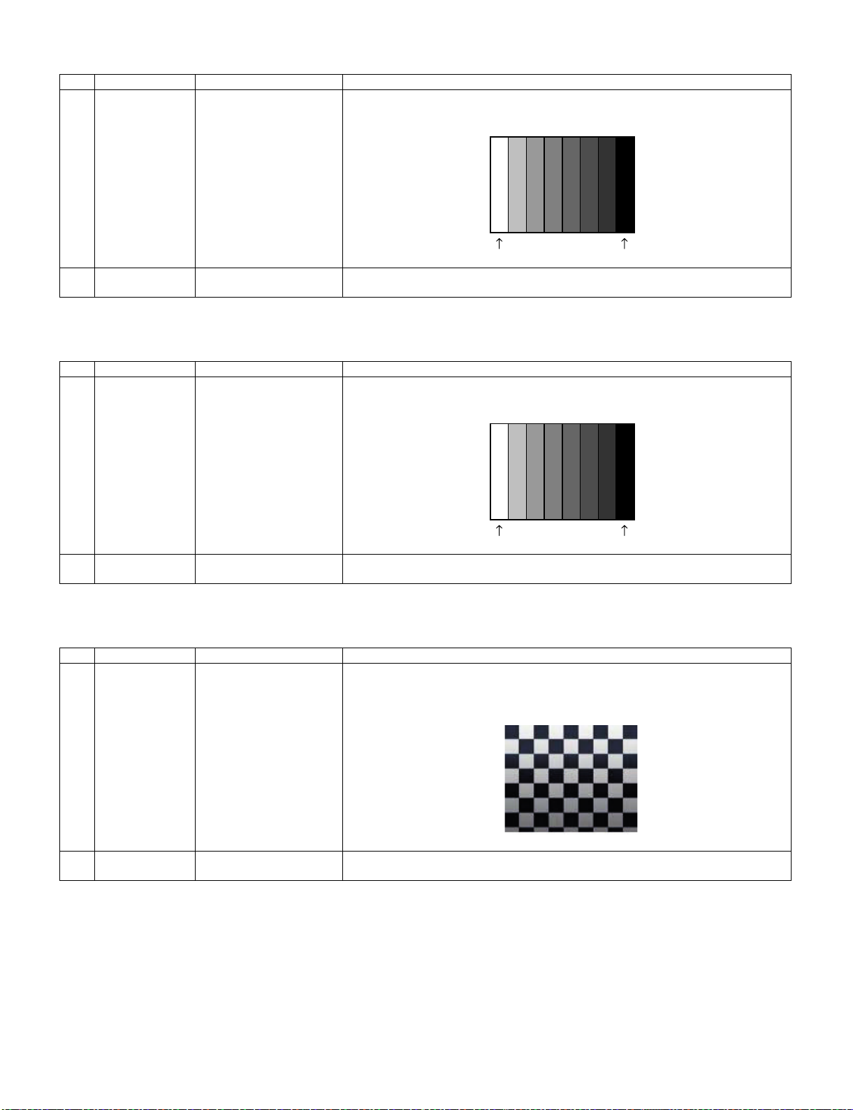
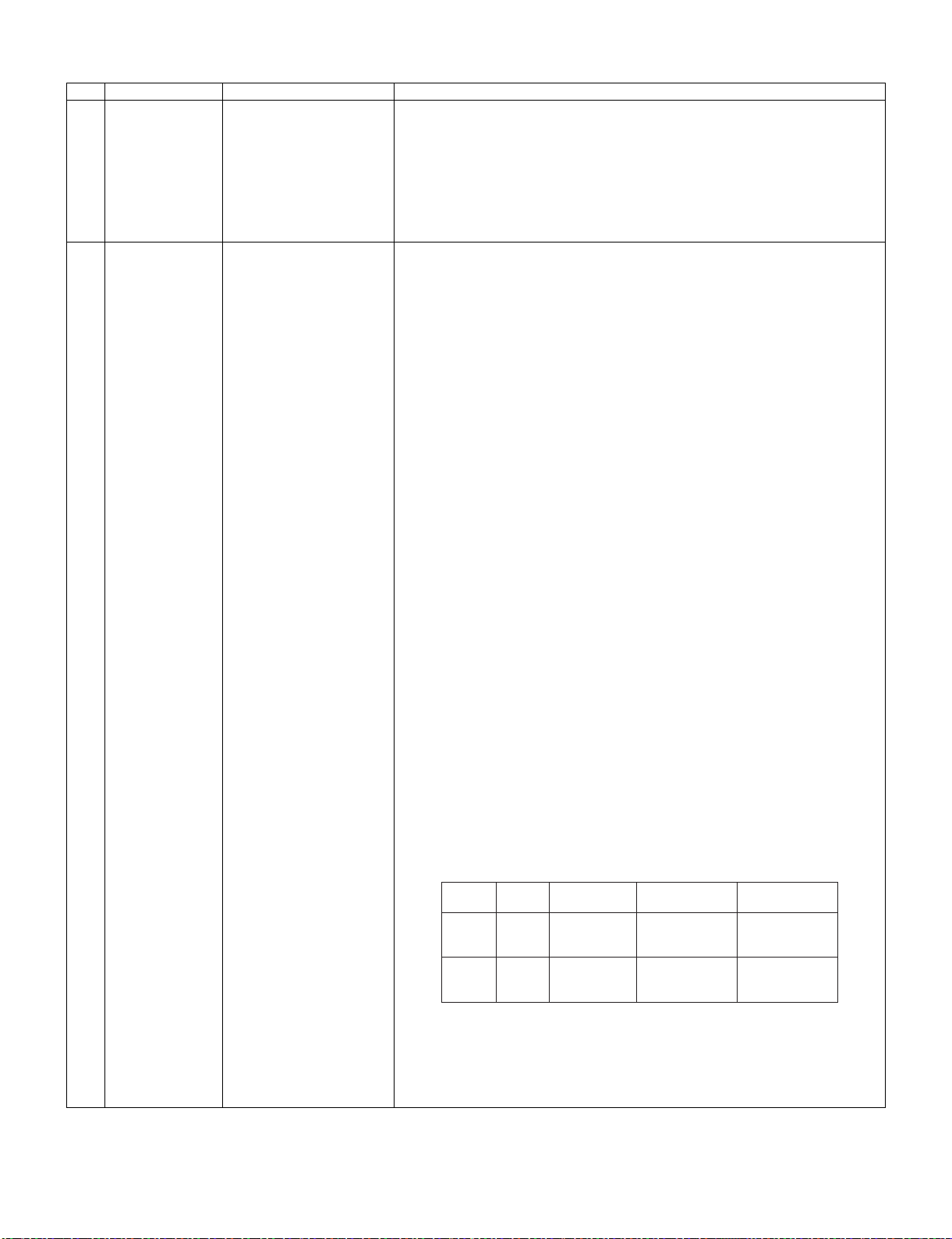
4.1.2 Component 15K 50Hz signal adjustment (COMP-SD)
Adjustment item Adjustment conditions Adjustment procedure
1 Adjustment [Signal]
COMP 15K 50Hz (576i)
100% Full-field Colour Bar
[Terminal]
INPUT 6 COMPONENT
Feed the COMPONENT 15K 50Hz (576i) 100% Full-field Colour Bar signal (100% colour
saturation) to INPUT 6 COMPONENT terminal.
100% white Black
2 Auto adjustment
performance
Process Mode page 4
(COMP SD)
1) At the related page, move cursor to [COMP SD ADJ], press ENTER.
2) [OK] appears when finished.
4.1.3 Component 33K 60Hz signal adjustment (COMP-HD)
Adjustment item Adjustment conditions Adjustment procedure
1 Adjustment [Signal]
COMP 33K 60Hz (1080i)
100% Full-field Colour Bar
[Terminal]
INPUT 6 COMPONENT
Feed the COMPONENT 33K 60Hz (1080i) 100% Full-field Colour Bar signal (100%
colour saturation) to INPUT 6 COMPONENT terminal.
100% white Black
2 Auto adjustment
performance
Process Mode page 5
(COMP HD)
1) At the related page, move cursor to [COMP HD ADJ], press ENTER.
2) [OK] appears when finished.
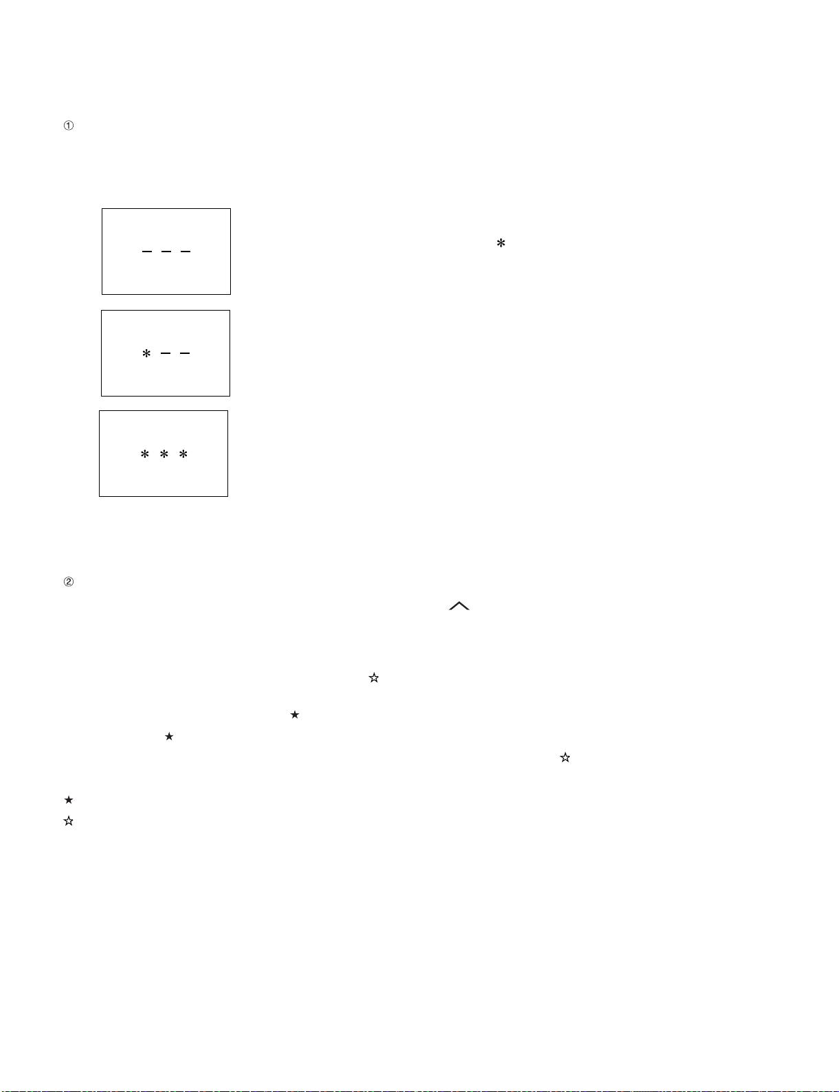
4.1.4 PC (ANALOG RGB) signal adjustment (PC-RGB)
Adjustment item Adjustment conditions Adjustment procedure
1 Adjustment [Signal]
XGA 60Hz
100% Checkered Pattern
[Terminal]
PC INPUT
Feed the XGA 60Hz 100% Checkered pattern signal (100% colour saturation) to PC
INPUT.
*Please make sure SYNC is OFF.
2 Auto adjustment
performance
Process Mode page 6
(PC-RGB)
1) At the related page, move cursor to [RGB ADJ], press ENTER.
2) [OK] appears when finished.
5 – 3
Page 19
4.2. White balance adjustment
Adjustment item Adjustment conditions Adjustment procedure
1 Adjustment Brightness : MAX
Set the luminance meter on
the center of the screen
LC-32M400M-BK/WH/RD
For the details of white balance adjustment procedure, please refer to white balance
adjustment spec for current model.
1) Confirm the set condition.
2) Connect the luminance meter CA-210.
3) Through RS-232C command, adjustment mode screen is displayed.
2 Auto Adjustment
performance
[command]
Adjustment Mode
KRSW0001
KKT10037
Setting
KYOF0001
OSDS0001
SBSL16_ _
Multi point adj. Mode
MSET0000
WBI20255
Point 2
WBI20204
MG2G****
MG2B****
MG2R****
Point 1
WBI10064
MG1G****
MG1B****
MG1R****
Write
MSET0003
[Adjustment Procedure]
1) Using the remote control, set the LCD TV to adjustment mode.
2) Measure Max brightness (Lmax).
3) Calculate min. brightness (Lmin)=Lmax/5000.
4) Measure Point 2 brightness (Lhigh).
5) Set the reference value R,G,B of Point 2 (R2)=3264 x (204/P2)
where P2=255 x [(Lhigh-Lmin)/(Lmax-Lmin)]1/2.2
6) Set the specified gradation for point 2, fix the most faint colour to get reference
value, adjust others 2 colour to minus adjustment for reference value of point 2.
7) Measure Point 1 brightness (Llow).
8) Set the reference value R,G,B of Point 1 (R1)=1024 x (64/P1)
where P1=255 x [(Llow-Lmin)/(Lmax-Lmin)]1/2.2
9) Set the specified gradation for point 1. Set G of point 1 to the default value [(R1 x G
value of point 2/R2), with fractions rounded] and adjust RB to the reference value of
point 1.
10)Adjusted value is writing at [command] MSET0003.
11)Set the G of point Max. to the default value (4080 x G value of point 2/R2). Set the
R,B Max. value [Gmax-G value of point 2 + (R,B value of pint 2)].
Set Max.Level
MGMG****
MGMB****
MGMR****
12)Shut down the AC power.
*Initial value at RGB 2 point : 3264
*Initial value at RGB 1 point : 1024
[Adjustment Value]
✩Specification data by engineering dept is set as reference.
[Reference value for adjustment reference]
Equipment: Luminance meter [Minolta CA-210]
Level
Point 2
ref.
values
Point 1
ref.
values
Ref. : For inspection, set the LCD TV as below.
AV MODE: [DYNAMIC] (Reset)
Monochrome: ON
Aging Time: Minimum 60 minutes
204
64
Spec
Data
x=0.272
y=0.277
x=0.272
y=0.277
Adjustment
Spec.
r0.0010
r0.0045
Inspection
Spec.
r0.0020
r0.0090
5 – 4
Page 20

LC-32M400M-BK/WH/RD
5. Factory setting
AC power is plug off after shipment setting is done.
CAUTION: Do not plug on again after shipment setting is done. If do, please re-do the shipment setting. Do not off with remote control.
Adjustment item Adjustment condition Adjustment procedure
Factory setting AC power off to exit the fac-
tory setting.
1) Setting is done with test remote control.
2) Press the “Factory Setting” key on the remote control continuously.
3) When Green background appears on screen and “K” mark disappears, setting is completed.
The followings are initialized to factory setting
1) User setting
2) Channel data (e. g. broadcast frequencies)
3) Manufacturer’s option settings
4) Password data
5) Setting values are set based on model destination
5 – 5
Page 21

LC-32M400M-BK/WH/RD
[2] USB Clone (Smart Loader)
1. Description
The Smart Loader is a function implemented in the service software to easily replicate the user settings of one TV into another.
These settings include (but not restricted to): picture and audio, turning set-up, language and country selection, PIN, child locked programs etc.
Factory adjustments are not copied as they are different for every TV.
The Smart Loader makes possible the user data to be stored in a memory device connected to the USB terminal of the TV that is used as reference
and later load those data into other TVs by using their respective USB terminal.
2. How it works
1. Enter USB clone menu (Smart Loader)
i) Press panel key [TV/VIDEO] and [VOL+] and AC on, it will go to password entry OSD
---
ii) Enter digit "369" then it will go to Smart Loader Menu
Smart Loader
SMLD Store [ ]
SMLD Restore [ ]
2. Smart Loader function
SMLD Store SMLD Restore
USB1st AQUOS TV
i) SMLD Store
• To copy all related data from TV -> USB and put under a fixed filename "SHP_SMLD.bin" (8kB).
ii) SMLD Restore
• To restore the related data from USB -> TV.
iii) SMLD Store and Restore execution
• To execute SMLD Store or SMLD Restore, highlight at selected item and press Enter.
• When copying is in process, "WAIT" is displayed.
• After cloning process is done, "OK" is displayed.
If cloning process is not finished due to error (e.g. no pendrive detected), "NG" is displayed.
2nd AQUOS TV
3. Exit USB Clone menu (Smart Loader)
i) To exit Smart Loader menu, plug off AC Cord.
5 – 6
Page 22
LC-32M400M-BK/WH/RD
[3] PUBLIC MODE SETTING PROCEDURE
1. How to start Public Mode
• There are the following two ways to get the public mode setup screen displayed.
1) Press the “TV/VIDEO” and “VOL (+)” keys on the set at once and turn on the power.
2) Get the password input screen displayed.
Procedure
• The input starts with the leftmost digit.
• Use the numeric keys [1] thru [9] and [10/0] keys on the remote controller.
The other keys are not acceptable.
• With a numeric-key input, “–” will change to “ “. The input position will move one digit to the right.
• With all the 3 digits entered, the password will be verified.
3) The 3-digit password is now verified.
The password [0] [2] [7] provides for the public mode screen. (This screen comes on with whatever adjustment process settings.)
With any other passwords, the screen changes to the normal mode.
In the adjustment process mode, turn on “PUBLIC MODE”. Also press the “CH ( )” and “VOL (+)” keys on the set at once and turn on the power.
2. How to exit Public Mode
There are the following ways to quit the public mode setup screen.
• Turn off “PUBLIC MODE” in the adjustment process mode. ( ) ← This way alone is not for quitting the setup screen, but for quitting the mode by
itself.
• Turn off the power with the “POWER” key. ( )
• Select “ENTER”.( )
• Move the cursor to “RESET” and press the “FLASHBACK” key. (Back to the normal mode screen) ( )
••• “PUBLIC MODE” stays on in the adjustment process mode.
••• The settings will be back to the factory ones.
3. Public Mode Setting Values
• With the factory settings made, the public mode settings get initialized. (The adjustment process remains intact.)
5 – 7
Page 23
LC-32M400M-BK/WH/RD
4. Public Mode Menu
The guidance is not displayed onscreen.
Setup procedure
• To move the cursor up and down, use the “cursor UP/DOWN” key (remote controller) and “CH ( )/( )” key (remote controller and set).
• To change the settings, use the “cursor RIGHT/LEFT” key (remote controller) and “VOL (+)/(–)” key (remote controller and set).
• To save new settings, keep the cursor at “Enter” and use the “cursor RIGHT/LEFT” key (remote controller) and “VOL (+)/(–)” key (remote controller
and set).
Public mode
Power on fixed
Maximum volume
Volume fixed
Volume fixed level
RC button
Panel button
Menu button
On screen display
Blue Screen
Input mode start
Input mode fixed
232C Powon
RC path through
Reset
Execute
5. On Setting Items
1. POWER ON FIXED
Selection Variable/Fixed
Default Variable
Explanation When set to “Fixed”, the power cannot be turned off with the power key on the remote control or main unit, and the image
Limit in setting • Power key on the main unit/remote control power supply key
Exception None
Remarks • Selection of “FIXED” assumes use of STB, etc.
2. MAXIMUM VOLUME
Selection Adjustment from 1 to 60 (no loop)
Default 60
Explanation Sound volume can not be adjusted higher than the preset value.
Limit in setting • When the sound volume is set lower than 59, only figures are displayed and the sound volume bar is not displayed.
Exception • In the item “VOLUME” of adjustment process, the sound volume can be set freely irrespective of this setting.
Remarks • Setting is valid only for the speakers of the unit. (As for the headphone, the sound volume can be set up to 60 irrespective
[Variable ]
[ 60]
[Variable ]
[ 20]
[Respond ]
[Respond ]
[Respond ]
[Yes ]
[No ]
[Normal ]
[Variable ]
[Disable ]
[Off ]
reception state is kept (it does not enter the standby state).
The power can be turned off by shutting off power supply from AC.
• OFF timer/ON timer
• When set to “Variable”, if the main power switch is set to off, the power is turned off after a wait of 1 second.
(Push-push switch only)
• Display ON/OFF in the hotel menu is controlled by the adjustment process “HOTEL POWERFIX”.
• When the power button is operated, a caution is displayed (it times out in 5 seconds).
(For the caution, refer to the power on fixed message sheet.)
* The caution is not displayed when in the adjustment process, hotel menu, default setting, MCL operation and auto preset
(Ch search operation).
The OSD display including the menu and this caution have priority over all others.
When “OSD display” (described below) is set to “Variable”, this caution is displayed as a special case.
• The maximum sound volume for ON-timer (Wake up timer) is limited also to the preset value.
of the limit.)
• In line output (sound volume variable), the sound volume can be adjusted from -60 to 0 irrespective of pre-adjusted value.
• When the sound volume is set higher than the MAX setting by the adjusting process or headphone, the sound volume control operation is prohibited for turn-up and the sound volume should be turned down to MAX in this state.
5 – 8
Page 24

LC-32M400M-BK/WH/RD
3. VOLUME FIXED
Selection Selection between “Variable” and “Fixed” (loop provided)
Default Variable
Explanation Sound volume is fixed and made invariable.
Limit in setting • The sound volume for the ON-timer (Wake up timer) is fixed also without display of menu. Besides, the setting is made
Exception • In the item “VOLUME” of adjustment process, the sound volume can be set freely irrespective of this setting.
Remarks • In “Variable” setting, the sound volume had been conventionally set at 1 but this operation has been abolished (and follows
4. VOLUME FIXED LEVEL
Selection Adjustment from 1 to 60 (no loop)
Default 20
Explanation The sound volume to be fixed by “Volume fixed” is determined.
Limit in setting None
Exception None
Remarks Setting is valid only when “Volume fixed” is selected for “fixed”.
impossible. (Basically, the menu is not displayed.)
• The following keys become invalid:
1) Sound volume Up/Down (VOL +/-) [for both remote control and the unit]
2) Mute (MUTE)
the last memory).
• The sound volume for the ON-time is not set at 1 either and the sound volume set value of the ON-timer before the hotel
mode is executed.
• Setting is valid only for the speakers of the unit. (As for the headphone, the sound volume can be set up to 60 irrespective
of the limit.)
• In line output (sound volume variable), the sound volume can be adjusted from -60 to 0 irrespective of pre-adjusted value.
• As for sound volume fixing and sound volume MAX level, the sound volume fixing has priority.
• Once the sound volume has been changed by adjustment process or headphone, it should be set back to the sound volume
preset by sound volume fixing level when the adjustment process ends or when the headphone is removed.
This must be confirmed actually by changing also the sound volume in accordance with setting.
5. R/C BUTTON
Selection Selection between “Respond”, “Limited” and “No respond” (loop provide)
Default Respond
Explanation Acceptability of keys by remote control is limited or reception of keys can be prohibited.
Limit in setting
Exception • Adjustment process, factory setting, inspection process and hotel only keys are valid irrespective of setting.
Remarks
6. PANEL BUTTON
Selection Selection between “Respond” and “No respond” (loop provide)
Default Respond
Explanation All the operations by keys (except the power key) of the unit can be invalidated.
Limit in setting
Exception • Inspection mode and hotel menu mode can be started irrespective of setting.
Remarks
7. MENU BUTTON
Selection Selection between “Respond” and “No respond” (loop provide)
Default Respond
Explanation In “No respond” setting, the menu operation by the menu key of the remote control and the menu key of the unit is invalidated.
Limit in setting • ON-timer (Wakeup Timer) is turned OFF.
Exception • Inspection mode and hotel menu mode can be started irrespective of setting.
Remarks
1) In “limited” setting, only power ON/OFF, sound volume , tuning and BACKLIGHT (brightness sensor) are
accepted.
2) In “No respond” setting, all the keys (including the power key) are not accepted.
• All the keys can be used in adjustment process, inspection mode and hotel menu irrespective of setting.
• All the keys can be used in adjustment process, inspection mode and hotel menu irrespective of setting.
• The following keys become invalid.
Wake-up timer and clock setting keys and all of the direct change keys to menu display
• All the keys can be used in adjustment process, inspection mode and hotel menu irrespective of setting.
5 – 9
Page 25

LC-32M400M-BK/WH/RD
8. ON SCREEN DISPLAY
Selection Selection between “Yes”, “No” (loop provide)
Default Yes
Explanation The following OSD displays are made ineffective.
Displays of menu group, channel call, sound volume bar and direct key call
Limit in setting • Set time of the OFF-timer (SLEEP TIMER) is cleared.
• Setting of the no-signal power-OFF (AUTO POWER OFF) is cleared to “OFF”.
• Setting of the no-operation power-OFF is cleared to “OFF”.
• Keys falling under any of the following items become invalid.
1) Appearance of screen changes and the sound changes.
2) Personal functions which are hard to restore.
Ex.) Screen display, menu, OFF-timer, ON-timer, AV MODE, screen size switching, clock setting, treble emphasis, AUDIO
ONLY, sound changeover, LANGUAGE, CLOSED CAPTION
Others • Simple input switching is generated. Those which are restored soon after leaving as they are and may be requested for
change by customer are not prohibited.
Ex.) Brightness sensor (BACKLIGHT) and PIC. FLIP
Exception • Such a caution which is displayed independently is displayed as it is.
9. BLUE SCREEN
Selection Selection between “Yes”, “No”
Default No
Explanation When no signal inputs, selecting the background color.
10.INPUT MODE START
Non-responding signal caution, TELE TEXT caution and power-ON fixing caution
Selected to “Yes”---Blue screen
Selected to “No”---No Blue screen
Selection Selection between “Normal”, “TV (CH~)” “INPUT1~8” (loop provide)
Default Normal
Explanation In power-ON, the input source to be started or channel can be set.
(In standard mode, the operation follows the last memory.)
About options • All the input sources in the model are made selectable.
• When the input/output switchable input source is selected and the input source is set to output, the setting of input/output
switching is changed to input at the execution of hotel menu. In addition, the input/output switching by menu is prohibited.
• In TV mode, the display of all channels is stopped and it is treated as an input source. At this time, the channel to be set follows the last memory and the content of the last memory is included in the notation by options. Ex.) TV (CH2), TV (CH4)
etc.
• The order of appearance of options in the hotel menu should agree with the order of toggles by input switching key.
Limit in setting • The display of channel setting menu and the channel setting operation are prohibited (except for MCL).
Exception None
Remarks • In setting at “Normal”, the setting of “Input mode fixed” is changed to “Variable” and selection should be prohibited.
11.INPUT MODE FIXED
Selection Selection between “Variable” and “Fixed” (loop provide)
Default – (Variable)
Explanation The input mode is fixed at the input source or the channel set at the “Input mode start” in 9 and other input sources and chan-
Limit in setting • With the execution of hotel mode, the input source is forced to change to that set by “Input mode start” and the channel
Exception None
Remarks • In the following case, setting is cancelled and mode is changed to “Variable”.
nels can be made non-selectable.
switching and input switching are prohibited thereafter.
• The following keys are invalidated.
CH , direct tuning button, FLASHBACK, input
*However, the keys (input switching and CH , keys) of the unit for menu operation remain valid.
When the setting of “Input mode start” is set to “Standard (Normal)”
12.232C POWON
Selection “Enable” and “Disable”
Default Disable
Explanation When in the standby state, power ON by the RS-232C command is enabled or disabled.
Limit in setting None
Exception None
Remarks
RS-232C power ON command “POWR1_ _ _ ”
5 – 10
Page 26

LC-32M400M-BK/WH/RD
13.RC PATH THROUGH
Selection “Off”, “On: TV RCE”, “On: TV RCD”
Default Off
Explanation Remote control signal output from the pin 9 of the RS-232C terminal and signal reception is enabled or disabled.
When set to “ON: TV RCE”, TV also receives signals. With “ON: TV RCD”, the remote control signal is output from the pin 9,
but TV does not respond to the remote control.
Limit in setting When set to “ON: TV RCD”, TV does not accept the remote control.
Exception None
Remarks
5 – 11
Page 27

LC-32M400M-BK/WH/RD
LC32M400MBK
CHAPTER 6. TROUBLESHOOTING TABLE
Service Manual
[1] TROUBLESHOOTING TABLE
No power (front LED failure to light up) or no startup (front LED failure to turn from red to green)
Is the AC cord connector tightly connected to the set? NO Reconnect the AC cord tightly and turn on the power again.
YES
Is the output voltage at pin (6), (7) and (8) of P9601 (13.0V line)
as specified?
YES
Are the wire harnesses and other cables properly connected in
the set?
YES
Is there the AC_DET and PNL_ON signal input at pins (11) and
(12) of P9601?
NO Replace the power unit.
NO Reconnect the wire harnesses and other cables properly in the
set.
NO Check the AC_DET signal line PNL_ON signal line.
YES
Are the DC/DC converter outputs and the output voltages along
the control lines as specified?
1) B5.6V (IC9603)
2) B1.26V (IC9604)
3) STB+3.3V (IC9606)
4) D2.6V (IC9607)
5) B5V (IC9608)
6) D3.3V (IC9609)
NO Check the DC/DC converters and the control lines. Replace
defective parts as required.
6 – 1
Page 28

LC-32M400M-BK/WH/RD
With [RF] signal input No video onscreen (1)
No video in the UHF/VHF reception
Is there IF output from the tuner pin(10) of TU1101 as specified? NO Check TU1101 and its peripheral circuits.
YES
Is there VIF input at pin 56 & 57 of IC3301? NO Check the circuit between TU1101 & IC3301.
YES
Are there the signal outputs of IC3301? NO Check IC3301 and its peripheral circuit.
YES
Check LVDS cable, LCD controller (incl. panel) and their periph-
eral circuits.
With <Video> signal input No video onscreen (2)
No external input video onscreen <INPUT 4>
Is INPUT 4 selected on the input select menu screen? NO Select INPUT 4 on the input select menu screen to pick up the
right input signal.
YES
Is there the video signal input at pin (35) of IC3301? NO Check the line between pin (4) of SC5201 and pin (35) of IC3301.
YES
Are there signal outputs of IC3301? NO Check IC3301 and its peripheral circuits.
YES
Check LVDS cable, LCD controller (incl. panel) and their peripheral circuits.
6 – 2
Page 29

LC-32M400M-BK/WH/RD
With <Video> signal input No video onscreen (3)
No external input video onscreen <INPUT 5>
Is INPUT 5 selected on the input select menu screen? NO Select INPUT 5 on the input select menu screen to pick up the
YES
Is there the video signal input at pin (33) of IC3301? NO Check the line between pin (6) of SC5201 and pin (33) of IC3301.
YES
Are there signal outputs of IC3301? NO Check IC3301 and its peripheral circuits.
YES
Check LVDS cable, LCD controller (incl. panel) and their periph-
eral circuits.
With <S-video> signal input No video onscreen (4)
right input signal.
No external input video onscreen <INPUT 4>
Is INPUT 4 selected on the input select menu screen? NO Select INPUT 4 on the input select menu screen to pick up the
right input signal.
YES
Are there the following signal inputs at the input terminals of
IC3301?
<S-video signal>
Are there the Y and C signal inputs at pins (30) and (29), respectively?
YES
Are there signal outputs of IC3301? NO Check IC3301 and its peripheral circuits.
YES
Check LCD controller (incl. panel) and their peripheral circuits.
NO <S-video signal>
Check the line between pins (1), (2) of SC5201 and pins (30)/(29)
of IC3301.
6 – 3
Page 30

LC-32M400M-BK/WH/RD
With <Component> signal input No video onscreen (5)
No external input video onscreen <INPUT 6>
Is INPUT 6 selected on the input select menu screen? NO Select INPUT 6 on the input select menu screen to pick up the
YES
Are there the Y, Pb and Pr signal inputs at pins (15), (13) and
(17) of IC3301 respectively?
YES
Is input waveform of IC3301 normal?
Y=(15) pin, Pb=(13) pin, Pr=(17) pin
YES
Check LVDS cable, LCD controller (incl. panel) and their periph-
eral circuits.
With <HDMI> signal input No video onscreen (6)
NO Check the line between pins (15)/(13)/(12) of SC5201 and pins
NO Check IC3301 and its peripheral circuits.
right input signal.
(15)/(13)/(17) of IC3301.
No external input video onscreen <INPUT 1>, <INPUT 2>,
<INPUT 3>
Is INPUT 1/INPUT 2/INPUT 3 selected on the menu screen? NO Select INPUT 1/INPUT 2/INPUT 3 on the input select menu
YES
Are there the signal input from HDMI connector to the following
input terminals of IC1551?
YES
Are there signal outputs from IC1551 to IC3301? NO Check peripheral circuits between IC1551 and IC3301.
YES
Are there signal outputs of IC3301? NO Check IC3301 and its peripheral circuits.
YES
Check LVDS cable, LCD controller (incl. panel) and their periph-
eral circuits.
NO Check IC1551 and their peripheral circuits.
screen to pick up the right signal input.
6 – 4
Page 31

LC-32M400M-BK/WH/RD
No audio heard (1)
No sound in the UHF/VHF reception.
Is the IF output from the tuner pin (10) of TU1101 as specified? NO Check TU1101 and its peripheral circuits.
YES
Is there the I2S signal input at pins (180), (181) of IC3301? NO Check IC3301 and its peripheral circuits.
YES
Is there L-ch audio signal input at pin(3) of IC2701? NO Check connection between IC3301 and IC2701 and its
Is there R-ch audio signal input at pin(7) of IC2701?
YES
Is the L-ch audio signal output at pin(27), (28), (29), (30) and (31) of
IC2701 normal?
Is the R-ch audio signal output at pin(11), (12), (13), (14) and (15) of
IC2701 normal?
NO Check IC2701 and its peripheral circuits.
peripheral circuits.
YES
Are the audio signal L-ch and R-ch output at (3)/(4) and (1)/(2) of
P2701 normal?
YES
Check speakers and their peripheral circuits.
NO Check circuit between IC2701 & P2701.
6 – 5
Page 32

LC-32M400M-BK/WH/RD
No audio heard (2)
No external audio heard
<INPUT 4>
Is there the L-ch audio signal input from pin (8) of input terminal
SC5201 to pin (77) of IC3301?
Is there the R-ch audio signal input from pin (9) of input terminal
SC5201 to pin (78) of IC3301?
<INPUT 5>
Is there the L-ch audio signal input from pin (10) of input terminal
SC5201 to pin (75) of IC3301?
Is there the R-ch audio signal input from pin (11) of input terminal
SC5201 to pin (76) of IC3301?
<INPUT 6>
Is there the L-ch audio signal input from pin (1) of input terminal
SC5202 to pin (72) of IC3301?
Is there the R-ch audio signal input from pin (2) of input terminal
SC5202 to pin (73) of IC3301?
YES
Is there the I2S signal input at pin (180), (181) of IC3301? NO Check IC3301 and its peripheral circuits.
YES
Is there L-ch audio signal input at pin(3) of IC2701? NO Check connection between IC3301 and IC2701 and its periphIs there R-ch audio signal input at pin(7) of IC2701?
eral circuits.
YES
Is the L-ch audio signal output at pin(27), (28), (29), (30) and (31)
of IC2701 normal?
Is the R-ch audio signal output at pin(11), (12), (13), (14) and (15)
of IC2701 normal?
YES
Are the audio signal L-ch and R-ch output at (3)/(4) and (1)/(2) of
P2701 normal?
YES
Check speakers and their peripheral circuits.
NO Check IC2701 and its peripheral circuits.
NO Check circuit between IC2701 & P2701.
6 – 6
Page 33

LC-32M400M-BK/WH/RD
No audio heard (3)
No HDMI sound heard. <INPUT 1>, <INPUT 2>, <INPUT 3>
(*INPUT 1 is digital audio.)
Does the HDMI image appear onscreen? NO Refer to “<INPUT 1> in No external input video onscreen
(HDMI)”.
YES
No audio output from <INPUT 1>, <INPUT 2>, <INPUT 3>. NO Check the EDID.
YES
Are waveforms input in to the pins of IC3301 normally and I2S output from the pins (255), (256) normally?
YES
Is there L-ch audio signal input at pin(3) of IC2701? NO Check connection between IC3301 and IC2701 and its periphIs there R-ch audio signal input at pin(7) of IC2701?
NO Check peripheral circuits between IC3301 and IC1551.
eral circuits.
YES
Is the L-ch audio signal output at pin(27), (28), (29), (30) and (31)
of IC2701 normal?
Is the R-ch audio signal output at pin(11), (12), (13), (14) and (15)
of IC2701 normal?
YES
Are the audio signal L-ch and R-ch output at (3)/(4) and (1)/(2) of
P2701 normal?
YES
Check speakers and their peripheral circuits.
NO Check IC2701 and its peripheral circuits.
NO Check circuit between IC2701 & P2701.
6 – 7
Page 34

LC-32M400M-BK/WH/RD
No audio heard (4)
No sound from the HDMI sound input terminal.
(INPUT 1 analog audio)
YES
Is there the L-ch audio signal input from pin (2) of external input
terminal J506 (HDMI AUDIO IN) to pin (70) of IC3301?
Is there the R-ch audio signal input from pin (3) of external input
terminal J506 (HDMI AUDIO IN) to pin (71) of IC3301?
YES
Are I2S signal output from the pins (180), (181) of IC3301 nor-
mally?
YES
Is there L-ch audio signal input at pin(3) of IC2701? NO Check connection between IC3301 and IC2701 and its periphIs there R-ch audio signal input at pin(7) of IC2701?
YES
Is the L-ch audio signal output at pin(27), (28), (29), (30) and (31)
of IC2701 normal?
Is the R-ch audio signal output at pin(11), (12), (13), (14) and (15)
of IC2701 normal?
NO Check peripheral circuits of IC3301.
eral circuits.
NO Check IC2701 and its peripheral circuits.
YES
Are the audio signal L-ch and R-ch output at (3)/(4) and (1)/(2) of
P2701 normal?
YES
Check speakers and their peripheral circuits.
NO Check circuit between IC2701 & P2701.
6 – 8
Page 35

LC-32M400M-BK/WH/RD
No audio heard (5)
No PC audio output
YES
Pin (2) of J506: Is L-ch input into the pin (70) of IC3301?
Pin (3) of J506: Is R-ch input into the pin (71) of IC3301?
YES
Are I2S signal output from the pins (180), (181) of IC3301 normally? NO Check peripheral circuits of IC3301.
YES
Is there L-ch audio signal input at pin(3) of IC2701? NO Check connection between IC3301 and IC2701 and its
Is there R-ch audio signal input at pin(7) of IC2701?
YES
Is the L-ch audio signal output at pin(27), (28), (29), (30) and (31) of
IC2701 normal?
Is the R-ch audio signal output at pin(11), (12), (13), (14) and (15) of
IC2701 normal?
NO Check IC2701 and its peripheral circuits.
peripheral circuits.
YES
Are the audio signal L-ch and R-ch output at (3)/(4) and (1)/(2) of
P2701 normal?
YES
Check speakers and their peripheral circuits.
NO Check circuit between IC2701 & P2701.
6 – 9
Page 36

LC-32M400M-BK/WH/RD
- MEMO -
6 – 10
Page 37

LC32M400MBK
CHAPTER 7. OVERALL WIRING/BLOCK DIAGRAM
[1] OVERALL WIRING DIAGRAM
LC-32M400M-BK/WH/RD
Service Manual
7 – 1
Page 38

LC-32M400M-BK/WH/RD
㪣
㪮㪧㪶㪚㪫㪩㪣㩿㪫㫉㫀㪸㫃㩷㫆㫅㫃㫐㪀
㪩
㪣
㪩
㪩
㪣
㪩
㩿㪉㪀
[2] SYSTEM BLOCK DIAGRAM
㪨㪪㪦㪚㪱㪘㪈㪎㪌㪮㪡㪱㪱㪰
㪟㪧㪛㪇㪶㪠
㪜㪜㪧㪩㪦㪤
㪠㪚㪌㪇㪏
㪭㪟㪠㪪㪉㪋㪚㪪㪇㪉㪡㪄㪈㪰
㪧㪚㩷㩷㪛㪪㪬㪙㩷㪈㪌㫇㫀㫅
㪪㪚㪌㪇㪉
㪪㪘㪥㪡㪠㩷㩿㪛㪪㪄㪇㪈㪙㪄㪇㪈㪤㪀
㪠㪥㪧㪬㪫㪎
㪟㪛㪤㪠㪆㪧㪚㩷㪣㪆㪩
㪨㪡㪘㪢㪡㪘㪇㪉㪋㪮㪡㪱㪱
㪠㪥㪧㪬㪫㪈㪆
㪠㪥㪧㪬㪫㪎
㪻㪸㫋㪸㩿㪋㪀
㪠㪥㪧㪬㪫㪈
㪟㪛㪤㪠㩷㪈
㪪㪚㪈㪌㪇㪈
㪺㫃㫂㩿㪉㪀
㪡㩷㪌㪇㪍
㪠㪉㪚㩿㪟㪛㪤㪠
㪭㪟㪠㪪㪉㪋㪚㪪㪇㪉㪡㪄
㪧㪚㩿㪩㪞㪙㪀
㪟㪛
㪭㪛
㪜㪜㪧㪩㪦㪤
㪠㪚㪈㪌㪇㪈
㪨㪪㪦㪚㪱㪘㪈㪋㪐㪮㪡㪨㪱㪰
㪟㪧㪛㪈㪶㪠
㪯㪫㪘㪣㩿㪈㪋㪅㪊㪈㪏㪤㪟㫑㪀
㪩㪚㪩㪪㪚㪘㪉㪋㪐㪮㪡㪨㪱㪰
㪠㪉㪚㩷㪘㪛㪛㪩㪜㪪㪪䋺㪘㪏
㪜㪜㪧㪩㪦㪤㩿㪟㪛㪚㪧㪀
㪩㪟㪄㪠㪯㪛㪈㪈㪇㪮㪡㪨㪱㪰
㪠㪉㪚㩷㪘㪛㪛㪩㪜㪪㪪䋺㪘㪋
㪜㪜㪧㪩㪦㪤㩿㪛㪘㪫㪘㪀
㪭㪟㪠㪩㪉㪋㪇㪍㪋㪘㪪㪄㪈㪰
㪠㪥㪧㪬㪫㪉 㪠㪥㪧㪬㪫㪊
㪟㪛㪤㪠㩷㪉
㪪㪚㪈㪌㪇㪉
㪺㫃㫂㩿㪉㪀
㪻㪸㫋㪸㩿㪋㪀
㪠㪉㪚㩿㪟㪛㪤㪠
㪟㪛㪤㪠㩷㩷㪪㪮
㪠㪚㪈㪌㪌㪈
㪙㪬㪈㪍㪇㪉㪏㪢
㪯㪊㪊㪇㪈
㪠㪚㪏㪋㪇㪊
㪠㪚㪏㪋㪇㪉
㪍㪋㪢㪹㫀㫋
㪜㪜㪧㪩㪦㪤
㪠㪚㪈㪌㪇㪉
㪭㪟㪠㪪㪉㪋㪚㪪㪇㪉㪡㪄
㪯㪠㪥㪆㪯㪦
㪨㪪㪦㪚㪱㪘㪈㪎㪌㪮㪡㪱㪱㪰
㪟㪧㪛㪉㪶㪠
㪠㪉㪚
㪠㪉
㪟㪛㪤㪠㩷㪊
㪪㪚㪈㪌㪇㪊
㪻㪸㫋㪸㩿㪋㪀
㪺㫃㫂㩿㪉㪀
㪠㪉㪚㩿㪟㪛㪤㪠
㪟㪛㪤㪠㩷㪠㪥㪈
㪟㪛㪤㪠㩷㪛㪛㪚㪈
㪧㪚㩷㪛㪛㪚
㪣㪆㪩㩷㪠㪥㪇
㪜㪜㪧㪩㪦㪤
㪠㪚㪈㪌㪇㪊
㪭㪟㪠㪪㪉㪋㪚㪪㪇㪉㪡㪄
㪟㪧㪛㪇㪶㪠㪥㪃
㪟㪧㪛㪈㪶㪠㪥㪃
㪟㪧㪛㪉㪶㪠㪥
㪟㪦㪫㪧㪣㪬㪞
㪭㪠㪝
㪪㪘㪮㩷㪝㫀㫃㫋㪼㫉
㪭㪠㪝㪂
㪭㪠㪝㩷㪠㪥
㪠㪉㪚㩷㪘㪛㪛㪩㪜㪪㪪䋺㪚㪇
㪩㪫㪬㪥㪨㪘㪇㪍㪎㪮㪡㪨㪱
㪠㪝
㪠㪝㩷㪘㪤㪧
㪭㪠㪝㪄
㪪㪠㪝
㪪㪘㪮㩷㪝㫀㫃㫋㪼㫉
㪪㪠㪝㩷㪠㪥
㪫㪬㪥㪜㪩
㪫㪬㪈㪈㪇㪈
㪪㪠㪝㪂㪪㪠㪝㪄
㪠㪉㪚
㪫㪜㪤㪧㩷㪪㪜㪥㪪㪦㪩
㪫㪟㪊㪊㪇㪈
㪩㪟㪄㪟㪯㪘㪇㪋㪎㪮㪡㪨㪱㪰
㪪㪘㪩㩿㪊㪀
㪧㪌㪋㪇㪊
㪩㪘㩿㪎㪀
㪦㪧㪚
㪠㪚㪈㪇㪈
㪠㪩㪶㪦㪧㪚
㪨㪧㪣㪞㪥㪙㪇㪋㪏㪮㪡㪱㪱
㪠㪩㩷㪩㪼㪺㫀㪼㫍㪼㫉
㪩㪤㪚㪈㪇㪈
㪪㪬㪙
㪣㪜㪛
㪣㪜㪛
㪛㪈㪇㪊㪆㪈㪇㪉
㪢㪜㪰
㪧㪦㪮㩷㪪㪮
㪈
㪫㪜㪩㪤㪠㪥㪘㪣
㪬㪥㪠㪫
㪪㪐㪇㪎
㪚㪦㪥㪫㪩㪦㪣㩷㪪㪮
㪪㪐㪇㪈㪄㪪㪐㪇㪌
㪣㪠㪥㪜㪶㪦㪬㪫㩷㪘㪤㪧
㪠㪚㪉㪎㪇㪉
㪭㪟㪠㪛㪩㪭㪍㪈㪉㪂㪂㪄㪠㪰
㪤㪘㪠㪥㩷㪪㪮
㪙㩷㫋㫆㩷㪙
㪪㪚㪌㪉㪇㪉
㪈㪌㫇㫀㫅
㪨㪚㪥㪚㪮㪘㪐㪏㪍㪮㪡㪨㪱㪰
㪙㩷㫋㫆㩷㪙
㪪㪚㪌㪉㪇㪈
㪈㪌㫇㫀㫅
㪚㪦㪤㪧㪦㪥㪜㪥㪫㩷㪈㩷㪠㪥
㪘㪬㪛㪠㪦㩷㪠㪥
㪡㪌㪌㪇㪊
㪤㪦㪥㪠㪫㪦㪩㩷㪣㪆㪩㩷㪦㪬㪫
㪡㪌㪌㪇㪋
㪚㪭㪙㪪㪈㩷㪠㪥
㪚㪭㪙㪪㪉㩷㪠㪥
㪡㪌㪌㪇㪉
㪪㪰㪆㪚㩷㪠㪥
㪡㪌㪌㪇㪈
㪢㪜㪰㪉
㵘㵘㵘㵘
㪘㪛㪚㩿㪋㪀
㪠㪩㪜㪤
㪦㪧㪚
㪠㫅㫋㪼㫉㪽㪸㪺㪼
㪠㪩
㪘㪛㩿㪇㪀
㪪㪘㪩㩿㪈㪀㪪㪘㪩㩿㪇㪀
㪚㪦㪤㪧㪶㪇
㪣㪆㪩㩷㪠㪥㪈
㪤㪦㪥㪠㪫㪦㪩
㪦㪬㪫㪶㪇
㪚㪭㪙㪪㪈
㪣㪆㪩㩷㪠㪥㪉
㪚㪭㪙㪪㪉
㪣㪆㪩㩷㪠㪥㪊
㪰㪆㪚㪇
㪠㪥㪧㪬㪫㪋㪶㪰㪃㪧㪹㪃㪧㫉
㪠㪥㪧㪬㪫㪋㩷㪣㪆㪩
㪣㪠㪥㪜㩷㪦㪬㪫㪇㩷㪣㪆㪩
㪠㪥㪧㪬㪫㪌㩷㪚㪭㪙㪪
㪠㪥㪧㪬㪫㪌㩷㪣㪆㪩
㪠㪥㪧㪬㪫㪍㩷㪚㪭㪙㪪
㪠㪥㪧㪬㪫㪍㩷㪣㪆㪩
㪠㪥㪧㪬㪫㪌㩷㪪㪰㪆㪪㪚
㪠㪥㪧㪬㪫㪌㪶㪪㩷㪻㪼㫋㪼㪺㫋
㪩㩷㪣㪜㪛
䌇㩷㪣㪜㪛
㪤㪘㪠㪥
㵘
㪠㪥㪭㪜㪩㪫㪜㪩
㪬㪥㪠㪫
AC
IN
㪠㪚㪌㪇㪊
㪭㪟㪠㪘㪟㪫㪈㪞㪇㪏㪮㪄
㪈㪰
IR
IR PASS
THROUGH
PIN 9
㪬㪘㪩㪫
㵘㵘㵘
㪩㪪㪉㪊㪉㪚㩷㪙㫌㪽㪽㪼㫉
㪠㪚㪌㪇㪈
㪭㪟㪠㪤㪊㪉㪉㪈㪜㪠㪧㪄㪈㪰
㪩㪪㪄㪉㪊㪉㪚
㪪㪚㪌㪇㪈
㪪㪘㪥㪡㪠㩷㩿㪛㪧㪄㪇㪊㪄㪇㪈㪤㪱㪈㪀
㵘㵘㵘㵘㵘㵘㵘
㪬㪪㪙㩷㪠㪝
㪬㪪㪙
㪡㪌㪇㪉
㪨㪪㪦㪚㪱㪘㪉㪏㪋㪮㪡㪨㪱
㪤㪪㪫㪐㪘㪏㪏㪋㪡㪣㩿㪮㪯㪞㪘㩷㪤㪦㪛㪜㪣㪀
㪏㪄㪹㫀㫋㩷㪮㪯㪞㪘㩷㪘㫅㪸㫃㫆㪾
㪩㪼㪽㩷㪥㫆㪅㪠㪚㪊㪊㪇㪈
㪩㪟㪄㪠㪯㪛㪇㪈㪏㪮㪡㪱㪱
㪟㪆㪮㩷㪩㪜㪪㪜㪫
㪛㪛㪩㪉㩿㪈㪉㪏㪤㪹㪀
㪩㪟㪄㪠㪯㪚㪐㪐㪋㪮㪡㪨㪱㪨
㪬㪪㪙㩷㪌㪭
㪠㪚㪌㪇㪐
㪭㪟㪠㪪㪈㪎㪇㪙㪌㪇㪬㪄㪈㪰
㪩㪜㪪㪜㪫
㪠㪚㪊㪊㪇㪉
㪭㪟㪠㪧㪪㪫㪏㪋㪉㪐㪬㪄㪈㪰
㪛㪩㪘㪤㩷㪠㪝
㪠㪚㪊㪌㪇㪈
㪭㪟㪠㪰㪛㪘㪈㪋㪏㪨㪱㪄㪈㪰
㪪㪧㪶
㪨㪧㪣㪞㪥㪘㪐㪍㪈㪮㪡㪱㪱㪰
㪪㪧㪶
㪪㪧 㪣
㪏㱅㩷㪌㪮
㪘㪬㪛㪠㪦㪶㪦㪬㪫
㪪㪧㪶
㪘㪬㪛㪠㪦㩷㪘㪤㪧
㪠㪚㪉㪎㪇㪈
㪪㪧
㪧㪉㪎㪇㪈
㪙㪣㪶㪦㪥
㪦㪝㪣
㪣㪘㪤㪧㩷㪜㪩㪩
㪘㪚㪶㪛㪜㪫
㪧㪪㪶㪦㪥
㪎㪅㪌㹢㪈㪊㪅㪌㪭
㪪㪫㪙
㪂㪌㪭
㪪㪫㪙
㪂㪊㪅㪊㪭
㪛㪉㪅㪍㪭
㪙㪌㪭
㪛㪊㪅㪊㪭
㪈㪅㪉㪍㪭
㪨㪚㪥㪚㪮㪙㪇㪈㪐㪮㪡㪨㪱㪰
㪧㪥㪣㪈㪉㪭
㪛㪘㪫㪘㩷㪘㩿㪈㪇㪀
㪣㪭㪛㪪㩷㩿㪏㩷㪙㫀㫋㪀
㪚㪣㪢㩷㪘㩿㪉㪀
㪪㪧㪠㩷㪠㪝
㪪㪧㪠
㪪㪧㩷㪤㪬㪫㪜
㪪㪧㪶
㪠㪯㪛㪊㪍㪏㪮㪡㪨㪱㪨
㪪㪧㪶
㪪㪧㪶
㪪㪧
㪏㱅㪌㪮
㪪㪧㪠㩷㪝㪣㪘㪪㪟
㪠㪚㪏㪋㪇㪈
㪩㪟㪄
㪋㪤㪙
㪪㪧㪠㩷㪝㪣㪘㪪㪟
㪮㪩㪠㪫㪜
㪚㪟㪜㪢㪜㪩㩷㪣㪘㪥㪛
㪪㪚㪉㪍㪇㪈
㪋㪈㫇㫀㫅
㪣㪮
㪛㪘㪫㪘㩷㪘㩿㪈㪇㪀
㪚㪣㪢㩷㪘
㪣㪢㪊㪈㪌㪫㪊㪣㪘㪎㪎㩿㪫㪼㫄㫇㫆㫉㪸
㪧㪦㪮㪜㪩
㪧㪘㪥㪜㪣
㪊㪉㩹㪮㪯㪞㪘
㪌㪇㪆㪍㪇㪟㫑
㫉㫐㪀
㪬㪥㪠㪫
7 – 2
Page 39

LC32M400MBK
CHAPTER 8. PRINTED WIRING BOARD ASSEMBLIES
[1] MAIN Unit
MAIN Unit
(Side-A)
LC-32M400M-BK/WH/RD
Service Manual
8 – 1
Page 40

LC-32M400M-BK/WH/RD
MAIN Unit
(Chip Parts Side-A)
8 – 2
Page 41

MAIN Unit
(Side-B)
LC-32M400M-BK/WH/RD
8 – 3
Page 42

LC-32M400M-BK/WH/RD
[2] IR OPC Unit
I/R OPC Unit
(Side-A)
I/R OPC Unit
(Chip Parts Side-A)
I/R OPC Unit
(Side-B)
8 – 4
Page 43

[3] TERMINAL Unit
LC-32M400M-BK/WH/RD
Terminal Unit
8 – 5
Page 44

LC-32M400M-BK/WH/RD
Terminal Unit
(Chip Parts)
8 – 6
Page 45

LC32M400MBK
CHAPTER 9. SCHEMATIC DIAGRAM
[1] DESCRIPTION OF SCHEMATIC DIAGRAM
1. VOLTAGE MEASUREMENT CONDITION:
1) The voltages at test points are measured on exclusive AC adaptor and the stable supply voltage of AC 110-240V. Signals are fed by a color bar signal generator for servicing purpose and the above voltages are measured with a 20k ohm/V tester.
2. INDICATION OF RESISTOR & CAPACITOR:
RESISTOR
1) The unit of resistance "Ω" is omitted.
(K=kΩ=1000Ω, M=MΩ).
2) All resistors are ± 5%, unless otherwise noted.
(K= ± 10%, F= ± 1%, D= ± 0.5%)
3) All resistors are 1/16W, unless otherwise noted.
CAPACITOR
1) All capacitors are µF, unless otherwise noted.
(P=pF=µµF).
2) All capacitors are 50V, unless otherwise noted.
CAUTION:
This circuit diagram is original one, therefore there may be a slight
difference from yours.
LC-32M400M-BK/WH/RD
Service Manual
SAFETY NOTES:
1) DISCONNECT THE AC PLUG FROM THE AC OUTLET
BEFORE REPLACING PARTS.
2) SEMICONDUCTOR HEAT SINKS SHOULD BE REGARDED AS
POTENTIAL SHOCK HAZARDS WHEN THE CHASSIS IS
OPERATING.
IMPORTANT SAFETY NOTICE:
PARTS MARKED WITH " " ( ) ARE IMPORTANT
FOR MAINTAINING THE SAFETY OF THE SET. BE SURE TO
REPLACE THESE PARTS WITH SPECIFIED ONES FOR MAINTAINING THE SAFETY AND PERFORMANCE OF THE SET.
9 – 1
Page 46

LC-32M400M-BK/WH/RD
[2] MAIN Unit
•MAIN Unit-1/11
9 – 2
Page 47

•MAIN Unit-2/11
LC-32M400M-BK/WH/RD
9 – 3
Page 48

LC-32M400M-BK/WH/RD
•MAIN Unit-3/11
9 – 4
Page 49

•MAIN Unit-4/11
LC-32M400M-BK/WH/RD
9 – 5
Page 50

LC-32M400M-BK/WH/RD
•MAIN Unit-5/11
9 – 6
Page 51

•MAIN Unit-6/11
LC-32M400M-BK/WH/RD
9 – 7
Page 52

LC-32M400M-BK/WH/RD
•MAIN Unit-7/11
9 – 8
Page 53

•MAIN Unit-8/11
LC-32M400M-BK/WH/RD
9 – 9
Page 54

LC-32M400M-BK/WH/RD
•MAIN Unit-9/11
9 – 10
Page 55

• MAIN Unit-10/11
LC-32M400M-BK/WH/RD
9 – 11
Page 56

LC-32M400M-BK/WH/RD
•MAIN Unit-11/11
9 – 12
Page 57

[3] IR OPC Unit
LC-32M400M-BK/WH/RD
9 – 13
Page 58

LC-32M400M-BK/WH/RD
[4] TERMINAL Unit
• TERMINAL Unit 1
9 – 14
Page 59

• TERMINAL Unit 2
LC-32M400M-BK/WH/RD
9 – 15
Page 60

LC-32M400M-BK/WH/RD
•TERMINAL Unit 3
9 – 16
Page 61

PartsGuide
LC-32M400M-BK/WH/RD
PARTS GUIDE
No. S51Q1LC32M40M
LCD COLOUR TELEVISION
LC-32M400M-BK
LC-32M400M-WH
MODELS
Note:
The reference numbers on the PWB
are arranged in alphabetical order.
[1] PRINTED WIRING BOARD
ASSEMBLIES
[2] LCD PANEL
[3] DKEYMF878FM01/FM02 (MAIN
Unit)
[4] DUNTKF879WE01 (IR/OPC Unit)
[5] DUNTKF885FM01 (TERMINAL
Unit)
LC-32M400M-RD
CONTENTS
[6] CABINET AND MECHANICAL
PARTS
[7] SUPPLIED ACCESSORIES
[8] PACKING PARTS (NOT
REPLACEMENT ITEM)
[9] SERVICE JIGS (USE FOR
SERVICING)
INDEX
Parts marked with " " are important for maintaining the safety of the set. Be sure to replace these
parts with specified ones for maintaining the safety and performance of the set.
This document has been published to be used
for after sales service only.
The contents are subject to change without notice.
Page 62

LC-32M400M-BK/WH/RD
NO. PARTS CODE
PRICE
RANK
NEW
MARK
PAR T
DELIVERY
[1] PRINTED WIRING BOARD ASSEMBLIES
N DKEYMF878FM01 BS N V MAIN Unit (Except for Philippines)
N DKEYMF878FM02 BS N V MAIN Unit (for Philippines)
N DUNTKF879WE01 AT N V IR/OPC Unit
N DUNTKF885FM01 AZ N V TERMINAL Unit
N RDENCA438WJPZ BM N V POWER Unit
N RUNTKA860WJPZ AW N V INVERTER Unit
[2] LCD PANEL
N R1LK315T3LW7AW CX V 32" LCD Panel Module Unit
[3] DKEYMF878FM01/FM02 (MAIN Unit)
C501 RC-KZA837WJQZY AB V Capacitor
C504 VCKYCY1HB104KY AA V Capacitor 0.1 50V Ceramic
C505 VCKYCY1HB104KY AA V Capacitor 0.1 50V Ceramic
C506 VCKYCY1HB104KY AA V Capacitor 0.1 50V Ceramic
C507 VCKYCY1HB104KY AA V Capacitor 0.1 50V Ceramic
C510 VCKYCZ1AB104KY AB V Capacitor 0.1 10V Ceramic
C519 VCCCCZ1HH102JY AA V Capacitor 1000p 50V Ceramic
C543 VCCCCZ1HH560JY AB V Capacitor 56p 50V Ceramic
C544 VCCCCZ1HH560JY AB V Capacitor 56p 50V Ceramic
C548 VCCCCZ1HH102JY AA V Capacitor 1000p 50V Ceramic
C553 VCCCCZ1HH102JY AA V Capacitor 1000p 50V Ceramic
C560 VCCCCZ1HH470JY AB V Capacitor 47p 50V Ceramic
C561 VCCCCZ1HH470JY AB V Capacitor 47p 50V Ceramic
C565 RC-KZA837WJQZY AB V Capacitor
C566 VCKYCZ1AB104KY AB V Capacitor 0.1 10V Ceramic
C568 RC-KZA837WJQZY AB V Capacitor
C569 RC-KZA837WJQZY AB V Capacitor
C570 VCKYCZ1AB104KY AB V Capacitor 0.1 10V Ceramic
C1103 VCKYCZ1AB104KY AB V Capacitor 0.1 10V Ceramic
C1105 RC-KZA837WJQZY AB V Capacitor
C1106 RC-KZA837WJQZY AB V Capacitor
C1107 RC-KZA837WJQZY AB V Capacitor
C1108 VCKYCZ1EB103KY AA V Capacitor 0.01 25V Ceramic
C1110 VCKYCZ1EB103KY AA V Capacitor 0.01 25V Ceramic
C1113 VCKYCZ1EB103KY AA V Capacitor 0.01 25V Ceramic
C1114 VCKYCZ1EB103KY AA V Capacitor 0.01 25V Ceramic
C1115 VCKYCZ1EB103KY AA V Capacitor 0.01 25V Ceramic
C1116 VCKYCZ1EB103KY AA V Capacitor 0.01 25V Ceramic
C1117 VCKYCZ1EB103KY AA V Capacitor 0.01 25V Ceramic
C1118 VCKYCZ1EB103KY AA V Capacitor 0.01 25V Ceramic
C1120 VCKYCZ1EB103KY AA V Capacitor 0.01 25V Ceramic
C1121 RC-KZA837WJQZY AB V Capacitor
C1501 RC-KZA837WJQZY AB V Capacitor
C1502 RC-KZA837WJQZY AB V
C1503 RC-KZA837WJQZY AB V Capacitor
C1504 VCKYCZ1EB103KY AA V Capacitor 0.01 25V Ceramic
C1505 VCKYCZ1EB103KY AA V Capacitor 0.01 25V Ceramic
C1506 VCKYCZ1EB103KY AA V Capacitor 0.01 25V Ceramic
C1551 VCKYCZ1HB102KY AB V Capacitor 1000p 50V Ceramic
C1552 VCKYCZ1EF104ZY AA V Capacitor 0.1 25V Ceramic
C1553 VCKYCZ1HB102KY AB V Capacitor 1000p 50V Ceramic
C1554 VCKYCZ1EF104ZY AA V Capacitor 0.1 25V Ceramic
C1555 VCKYCZ1EF104ZY AA V Capacitor 0.1 25V Ceramic
C1556 VCKYCZ1HB102KY AB V Capacitor 1000p 50V Ceramic
C1557 VCKYCZ1EF104ZY AA V Capacitor 0.1 25V Ceramic
C1558 VCKYCZ1HB102KY AB V Capacitor 1000p 50V Ceramic
C1559 VCKYCZ1EF104ZY AA V Capacitor 0.1 25V Ceramic
C1560 VCKYCZ1HB102KY AB V Capacitor 1000p 50V Ceramic
C1561 VCKYCZ1EF104ZY AA V Capacitor 0.1 25V Ceramic
C1562 VCKYCZ1HB102KY AB V Capacitor 1000p 50V Ceramic
C1563 RC-KZA520WJQZY AA V Capacitor
C1564 VCKYCZ1HB102KY AB V Capacitor 1000p 50V Ceramic
C1565 VCKYCZ1EF104ZY AA V Capacitor 0.1 25V Ceramic
C1566 VCKYCZ1HB102KY AB V Capacitor 1000p 50V Ceramic
C1567 VCKYCZ1EF104ZY AA V Capacitor 0.1 25V Ceramic
C2701 VCKYCZ1HB102KY AB V Capacitor 1000p 50V Ceramic
C2702 RC-KZA621WJQZY AA V Capacitor
C2703 RC-KZA067WJZZY AB V Capacitor
C2705 VCCCCZ1HH821JY AA V Capacitor 820p 50V Ceramic
C2706 RC-KZA621WJQZY AA V Capacitor
C2707 VCCCCZ1HH821JY AA V Capacitor 820p 50V Ceramic
C2708 RC-KZA837WJQZY AB V Capacitor
C2709 VCKYCZ1EF104ZY AA V Capacitor 0.1 25V Ceramic
C2713 RC-KZA621WJQZY AA V Capacitor
C2714 RC-KZA621WJQZY AA V Capacitor
C2715 VCKYCZ1HB102KY AB V Capacitor 1000p 50V Ceramic
C2716 RC-KZA837WJQZY AB V Capacitor
C2717
C2718 VCKYCZ1EF104ZY AA V Capacitor 0.1 25V Ceramic
C2719 VCCCCZ1HH101JY AB V Capacitor 100p 50V Ceramic
C2720 VCKYCZ1EF104ZY AA V Capacitor 0.1 25V Ceramic
C2721 RC-KZA621WJQZY AA V Capacitor
C2722 RC-KZA621WJQZY AA V Capacitor
C2723 RC-KZA621WJQZY AA V Capacitor
RC-KZA838WJQZY AB N V Capacitor
Capacitor
DESCRIPTION
2
Page 63

LC-32M400M-BK/WH/RD
NO. PARTS CODE
PRICE
RANK
NEW
MARK
PAR T
DELIVERY
[3] DKEYMF878FM01/FM02 (MAIN Unit)
C2724 RC-KZA621WJQZY AA V Capacitor
C2725 VCKYCZ1EF104ZY AA V Capacitor 0.1 25V Ceramic
C2726 VCKYCZ1EF104ZY AA V Capacitor 0.1 25V Ceramic
C2727 VCKYCZ1EF104ZY AA V Capacitor 0.1 25V Ceramic
C2728 VCKYCZ1EF104ZY AA V Capacitor 0.1 25V Ceramic
C2729 VCKYTV1EB224KY AA V Capacitor 0.22 25V Ceramic
C2730 VCKYTV1EB224KY AA V Capacitor 0.22 25V Ceramic
C2731 VCCCCZ1HH151JY AB V Capacitor 150p 50V Ceramic
C2732 VCCCCZ1HH151JY AB V Capacitor 150p 50V Ceramic
C2733 VCCCCZ1HH151JY AB V Capacitor 150p 50V Ceramic
C2734 VCCCCZ1HH151JY AB V Capacitor 150p 50V Ceramic
C2735 VCKYCY1HB104KY AA V Capacitor 0.1 50V Ceramic
C2736 VCKYCY1HB104KY AA V Capacitor 0.1 50V Ceramic
C2737 VCKYCY1HB104KY AA V Capacitor 0.1 50V Ceramic
C2738 VCKYCY1HB104KY AA V Capacitor 0.1 50V Ceramic
C2739 RC-KZA838WJQZY AB N V Capacitor
C2740 RC-KZA838WJQZY AB N V Capacitor
C2741 VCKYCY1AB105KY AB V Capacitor 1 10V Ceramic
C2757 RC-KZA115WJZZY AB V Capacitor
C2758 RC-KZA115WJZZY AB V Capacitor
C3301 VCKYCZ1HB221KY AA V Capacitor 220p 50V Ceramic
C3302 VCKYCZ1HB221KY AA V Capacitor 220p 50V Ceramic
C3303 VCKYCZ1HB221KY AA V Capacitor 220p 50V Ceramic
C3304 VCKYCZ1HB221KY AA V Capacitor 220p 50V Ceramic
C3305 VCKYCZ1AB473KY AB V Capacitor 0.047 10V Ceramic
C3306 VCKYCZ1AB473KY AB V Capacitor 0.047 10V Ceramic
C3307 VCKYCZ1AB473KY AB V Capacitor 0.047 10V Ceramic
C3308 VCKYCZ1AB473KY AB V Capacitor 0.047 10V Ceramic
C3309 VCKYCZ1AB473KY AB V Capacitor 0.047 10V Ceramic
C3310 VCKYCZ1AB473KY AB V Capacitor 0.047 10V Ceramic
C3311 VCKYCZ1AB473KY AB V Capacitor 0.047 10V Ceramic
C3312 VCKYCZ1AB473KY AB V Capacitor 0.047 10V Ceramic
C3313 VCKYCZ1AB473KY AB V Capacitor 0.047 10V Ceramic
C3314 VCKYCZ1AB473KY AB V
C3315 RC-KZA115WJZZY AB V Capacitor
C3316 RC-KZA115WJZZY AB V Capacitor
C3317 RC-KZA115WJZZY AB V Capacitor
C3318 RC-KZA115WJZZY AB V Capacitor
C3319 RC-KZA115WJZZY AB V Capacitor
C3320 RC-KZA115WJZZY AB V Capacitor
C3321 RC-KZA115WJZZY AB V Capacitor
C3322 RC-KZA115WJZZY AB V Capacitor
C3323 VCKYCZ1AB473KY AB V Capacitor 0.047 10V Ceramic
C3324 VCKYCZ1AB473KY AB V Capacitor 0.047 10V Ceramic
C3325 VCKYCZ1AB473KY AB V Capacitor 0.047 10V Ceramic
C3326 VCKYCZ1AB473KY AB V Capacitor 0.047 10V Ceramic
C3327 VCKYCZ1AB473KY AB V Capacitor 0.047 10V Ceramic
C3328 VCKYCZ1HB102KY AB V Capacitor 1000p 50V Ceramic
C3329 VCKYCZ1AB104KY AB V Capacitor 0.1 10V Ceramic
C3330 VCKYCZ1AB104KY AB V Capacitor 0.1 10V Ceramic
C3331 VCKYCZ1AB104KY AB V Capacitor 0.1 10V Ceramic
C3332 VCKYCZ1AB104KY AB V Capacitor 0.1 10V Ceramic
C3333 VCKYCZ1AB104KY AB V Capacitor 0.1 10V Ceramic
C3334 VCKYCZ1AB104KY AB V Capacitor 0.1 10V Ceramic
C3335 VCKYCZ1AB104KY AB V Capacitor 0.1 10V Ceramic
C3336 VCKYCZ1AB104KY AB V Capacitor 0.1 10V Ceramic
C3337 VCKYCZ1AB104KY AB V Capacitor 0.1 10V Ceramic
C3338 VCKYCZ1AB104KY AB V Capacitor 0.1 10V Ceramic
C3339 VCKYCZ1AB104KY AB V Capacitor 0.1 10V Ceramic
C3340 VCKYCZ1AB104KY AB V Capacitor 0.1 10V Ceramic
C3341 VCKYCZ1AB104KY AB V Capacitor 0.1 10V Ceramic
C3342 VCKYCZ1AB104KY AB V Capacitor 0.1 10V Ceramic
C3343 VCKYCZ1AB104KY AB V Capacitor 0.1 10V Ceramic
C3344 VCKYCZ1EB103KY AA V Capacitor 0.01 25V Ceramic
C3345 VCKYCZ1AB104KY AB V Capacitor 0.1 10V Ceramic
C3346 VCKYCZ1AB104KY AB V Capacitor 0.1 10V Ceramic
C3347 RC-KZA520WJQZY AA V Capacitor
C3348
C3349 VCKYCZ1AB104KY AB V Capacitor 0.1 10V Ceramic
C3350 VCKYCZ1AB104KY AB V Capacitor 0.1 10V Ceramic
C3351 VCKYCZ1AB104KY AB V Capacitor 0.1 10V Ceramic
C3352 VCKYCZ1AB104KY AB V Capacitor 0.1 10V Ceramic
C3353 RC-KZA837WJQZY AB V Capacitor
C3354 RC-KZA837WJQZY AB V Capacitor
C3355 VCKYCZ1AB104KY AB V Capacitor 0.1 10V Ceramic
C3356 VCKYCZ1AB104KY AB V Capacitor 0.1 10V Ceramic
C3357 VCCCCZ1HH100DY AB V Capacitor 10p 50V Ceramic
C3358 VCCCCZ1HH120JY AB V Capacitor 12p 50V Ceramic
C3359 RC-KZA837WJQZY AB V Capacitor
C3360 VCKYCZ1AB104KY AB V Capacitor 0.1 10V Ceramic
C3361 VCKYCZ1AB104KY AB V Capacitor 0.1 10V Ceramic
C3362 VCKYCZ1AB104KY AB V Capacitor 0.1 10V Ceramic
C3363 VCCCCZ1HH101JY AB V Capacitor 100p 50V Ceramic
C3364 RC-KZA837WJQZY AB V Capacitor
C3365 RC-KZA837WJQZY AB V Capacitor
VCKYCZ1AB104KY AB V Capacitor 0.1 10V Ceramic
Capacitor 0.047 10V Ceramic
DESCRIPTION
3
Page 64

LC-32M400M-BK/WH/RD
NO. PARTS CODE
PRICE
RANK
NEW
MARK
PAR T
DELIVERY
[3] DKEYMF878FM01/FM02 (MAIN Unit)
C3366 VCKYCZ1AB104KY AB V Capacitor 0.1 10V Ceramic
C3367 VCKYCZ1AB104KY AB V Capacitor 0.1 10V Ceramic
C3368 VCKYCZ1AB104KY AB V Capacitor 0.1 10V Ceramic
C3369 VCKYCZ1AB104KY AB V Capacitor 0.1 10V Ceramic
C3370 RC-KZA621WJQZY AA V Capacitor
C3371 VCKYCZ1AB104KY AB V Capacitor 0.1 10V Ceramic
C3372 VCKYCZ1AB104KY AB V Capacitor 0.1 10V Ceramic
C3373 VCKYCZ1AB104KY AB V Capacitor 0.1 10V Ceramic
C3374 VCKYCZ1AB104KY AB V Capacitor 0.1 10V Ceramic
C3375 RC-KZA837WJQZY AB V Capacitor
C3376 VCKYCZ1AB104KY AB V Capacitor 0.1 10V Ceramic
C3377 VCCCCZ1HH101JY AB V Capacitor 100p 50V Ceramic
C3378 VCCCCZ1HH101JY AB V Capacitor 100p 50V Ceramic
C3379 VCCCCZ1HH101JY AB V Capacitor 100p 50V Ceramic
C3502 VCKYCZ1AB104KY AB V Capacitor 0.1 10V Ceramic
C3504 VCKYCZ1AB104KY AB V Capacitor 0.1 10V Ceramic
C3506 VCKYCZ1AB104KY AB V Capacitor 0.1 10V Ceramic
C3507 VCKYCZ1AB104KY AB V Capacitor 0.1 10V Ceramic
C3508 RC-KZA837WJQZY AB V Capacitor
C3509 VCKYCZ1AB104KY AB V Capacitor 0.1 10V Ceramic
C3510 VCKYCZ1AB104KY AB V Capacitor 0.1 10V Ceramic
C3511 VCKYCZ1AB104KY AB V Capacitor 0.1 10V Ceramic
C3514 VCKYCZ1AB104KY AB V Capacitor 0.1 10V Ceramic
C3515 VCKYCZ1AB104KY AB V Capacitor 0.1 10V Ceramic
C3517 VCKYCZ1AB104KY AB V Capacitor 0.1 10V Ceramic
C3518 RC-KZA837WJQZY AB V Capacitor
C3519 RC-KZA837WJQZY AB V Capacitor
C8401 VCKYCZ1AB104KY AB V Capacitor 0.1 10V Ceramic
C8402 VCKYCZ1AB104KY AB V Capacitor 0.1 10V Ceramic
C8403 VCKYCZ1AB104KY AB V Capacitor 0.1 10V Ceramic
C9603 VCKYCZ1HB102KY AB V Capacitor 1000p 50V Ceramic
C9604 VCKYCZ1CB333KY AA V Capacitor 0.033 16V Ceramic
C9606 VCKYCZ1CB333KY AA V Capacitor 0.033 16V Ceramic
C9608 VCKYCZ1EB103KY AA V
C9609 RC-KZA838WJQZY AB N V Capacitor
C9610 RC-KZA838WJQZY AB N V Capacitor
C9611 VCKYCZ1EB103KY AA V Capacitor 0.01 25V Ceramic
C9612 VCKYCY1HB222KY AA V Capacitor 2200p 50V Ceramic
C9613 VCKYCZ1CB103KY AB V Capacitor 0.01 16V Ceramic
C9618 RC-KZA837WJQZY AB V Capacitor
C9619 VCKYCZ1HB471KY AB V Capacitor 470p 50V Ceramic
C9621 RC-KZA837WJQZY AB V Capacitor
C9622 RC-KZA837WJQZY AB V Capacitor
C9623 RC-KZA837WJQZY AB V Capacitor
C9625 RC-KZA837WJQZY AB V Capacitor
C9626 RC-KZA837WJQZY AB V Capacitor
C9627 RC-KZA837WJQZY AB V Capacitor
C9629 RC-KZA837WJQZY AB V Capacitor
C9630 RC-KZA837WJQZY AB V Capacitor
C9631 RC-KZA837WJQZY AB V Capacitor
C9632 RC-KZA837WJQZY AB V Capacitor
C9633 RC-KZA837WJQZY AB V Capacitor
C9635 VCKYCZ1HB221KY AA V Capacitor 220p 50V Ceramic
C9636 RC-KZA838WJQZY AB N V Capacitor
C9637 RC-KZA838WJQZY AB N V Capacitor
C9638 VCKYCY1HB104KY AA V Capacitor 0.1 50V Ceramic
D503 RH-EXA633WJQZY AA V Diode RKZ5.6B2KG
D510 VHDBAV70+++-1Y AB V Diode BAV70,215
D1101 VHD1SS390++-1Y AB V Diode 1SS390TE61
D1510 VHD0203CTRF-1Y AB V Diode HRC0203CTRF-E
D1511 VHD0203CTRF-1Y AB V Diode HRC0203CTRF-E
D1512 VHD0203CTRF-1Y AB V Diode HRC0203CTRF-E
D1516 VHD0203CTRF-1Y AB V Diode HRC0203CTRF-E
D1517 VHD0203CTRF-1Y AB V Diode HRC0203CTRF-E
D1518 VHD0203CTRF-1Y AB V Diode HRC0203CTRF-E
D3301 VHD0203CTRF-1Y AB V Diode HRC0203CTRF-E
D9601 VHD0203CTRF-1Y AB V Diode HRC0203CTRF-E
FB1101
FB1102 RBLN-A191WJZZY AB V Ferrite Core
FB3301 RBLN-A192WJZZY AA V Ferrite Core
FB3302 RBLN-A192WJZZY AA V Ferrite Core
FB3303 RBLN-A192WJZZY AA V Ferrite Core
FB3304 RBLN-A192WJZZY AA V Ferrite Core
FB3305 RBLN-A192WJZZY AA V Ferrite Core
FB3306 RBLN-A192WJZZY AA V Ferrite Core
FB3307 RBLN-A192WJZZY AA V Ferrite Core
FB3308 RBLN-A192WJZZY AA V Ferrite Core
FL1101 RFILCA067WJZZ AG N V Filter
FL1102 RFILCA066WJZZ AG N V Filter
FL3501 RFILNA119WJZZY AC V Filter
IC501 VHIM3221EIP-1Y AK V IC MAX3221EIPWRG4
IC503 VHIAHT1G08W-1Y AD V IC 74AHCT1G08GW/G,125
IC508 RH-IXD169WJQZS AL N V IC PC EDID
IC509 VHIS170B50U-1Y AD V IC S-1170B50UC-OUJTFG
IC1501 RH-IXD170WJQZS AL N V IC HDMI 1 EDID
RBLN-A191WJZZY AB V Ferrite Core
Capacitor 0.01 25V Ceramic
DESCRIPTION
4
Page 65

LC-32M400M-BK/WH/RD
NO. PARTS CODE
PRICE
RANK
NEW
MARK
PAR T
DELIVERY
[3] DKEYMF878FM01/FM02 (MAIN Unit)
IC1502 RH-IXD189WJQZS AL N V IC HDMI 3 EDID
IC1503 RH-IXD188WJQZS AL N V IC HDMI 2 EDID
IC1551 VHIBU16028K-1Q AP V IC BU16028KV
IC2701 VHIYDA148QZ-1Y AL V IC YDA148-QZE2
IC2702 VHIDRV612++-1Y AF N V IC
IC3301 RH-IXD018WJZZQ BA V IC MST9A884JL-LF
IC3302 VHIPST8429U-1Y AC V IC-PST8429UR
IC3501 RH-IXC994WJQZQ AN V IC H5DU1262GTR-E3C
IC8401 RH-IXD368WJN1Q AS N V IC
IC8402 VHIR24064AS-1Y AD V IC R1EX24064ASAS0A
IC8403 RH-IXD110WJQZY AG V IC CAT24C08
IC9601 VHIPST8429U-1Y AC V IC-PST8429UR
IC9603 VHIBD9328EF-1Y AF V IC BD9328EFJ-E2
IC9604 VHIBD9328EF-1Y AF V IC BD9328EFJ-E2
IC9606 VHIS170B35U-1Y AE V IC S-1170B35UC-OTUTFG
IC9607 VHIS170B26U-1Y AD V IC S-1170B26UC-OTLTFG
IC9608 VHIS170B50U-1Y AD V IC S-1170B50UC-OUJTFG
IC9609 VHIS170B33U-1Y AD V IC S-1170B33UC-OTSTFG
J502 QSOCZA284WJQZ AC N V Socket
J506 QJAKJA024WJZZ AD V Jack
L501 RCILFA154WJZZY AC V Coil
L1103 VPSBNR82JR34NY AB V Peaking Coil 0.82µH
L2601 RCILFA362WJZZY AC V Coil
L2604 RCILFA362WJZZY AC V Coil
L2605 RCILFA362WJZZY AC V Coil
L2701 RCILPB301WJQZY AC N V Coil
L2702 RCILPB301WJQZY AC N V Coil
L2703 RCILPB301WJQZY AC N V Coil
L2704 RCILPB301WJQZY AC N V Coil
L9602 RCILPB014WJQZY AC V Coil
L9603 RCILPB510WJQZY AC V Coil
P2701 QPLGNA961WJZZY AD V Plug
P9601 QPLGNA168WJZZY AF V Plug
Q1101 VS2SC2735//1EY AC V Transistor 2SC2735JC21TL
Q1105 VSRT1N441U/-1Y AB V Transistor RT1N441U-T111-1
Q1501 VSRT1N441U/-1Y AB V Transistor RT1N441U-T111-1
Q1502 VSRT1N441U/-1Y AB V Transistor RT1N441U-T111-1
Q1503 VSRT1N441U/-1Y AB V Transistor RT1N441U-T111-1
Q1504 VSRT1N441U/-1Y AB V Transistor RT1N441U-T111-1
Q1505 VSRT1N441U/-1Y AB V Transistor RT1N441U-T111-1
Q1506 VSRT1N441U/-1Y AB V Transistor RT1N441U-T111-1
Q1507 VSRT1N441U/-1Y AB V Transistor RT1N441U-T111-1
Q1508 VSRT1N441U/-1Y AB V Transistor RT1N441U-T111-1
Q1509 VSRT1N441U/-1Y AB V Transistor RT1N441U-T111-1
Q2701 VSRT1N441U/-1Y AB V Transistor RT1N441U-T111-1
Q2703 VSRT1N441U/-1Y AB V Transistor RT1N441U-T111-1
Q3302 VSRT1N141U/-1Y AB V Transistor RT1N141U-T111-1
Q9602 VSRT1N141U/-1Y AB V Transistor RT1N141U-T111-1
Q9603 VSKTA1535T+-1Y AC N V Transistor KTA1535T-RTK/P
R502 VRS-TV1JD101JY AA V Resistor 100 1/16W Metal Oxide
R503 VRS-TV1JD101JY AA V Resistor 100 1/16W Metal Oxide
R505 VRS-CZ1JF472JY AA V Resistor 4.7k 1/16W Metal Oxide
R506 VRS-CZ1JF101JY AA V Resistor 100 1/16W Metal Oxide
R507 VRS-TV1JD101JY AA V Resistor 100 1/16W Metal Oxide
R577 VRS-CZ1JF183JY AA V Resistor 18k 1/16W Metal Oxide
R578 VRS-CZ1JF183JY AA V Resistor 18k 1/16W Metal Oxide
R581 VRS-CZ1JF123JY AA V Resistor 12k 1/16W Metal Oxide
R582 VRS-TQ2EF750JY AA V Resistor 75 1/4W Metal Oxide
R583 VRS-TQ2EF750JY AA V Resistor 75 1/4W Metal Oxide
R584 VRS-TQ2EF750JY AA V Resistor 75 1/4W Metal Oxide
R585 VRS-CZ1JF000JY AA V Resistor 0 1/16W Metal Oxide
R586 VRS-CZ1JF000JY AA V Resistor 0 1/16W Metal Oxide
R590 VRS-CZ1JF123JY AA V Resistor 12k 1/16W Metal Oxide
R607 VRS-CZ1JF473JY AA V Resistor 47k 1/16W Metal Oxide
R608 VRS-CZ1JF473JY AA V Resistor 47k 1/16W Metal Oxide
R610 VRS-CZ1JF222JY AA V Resistor 2.2k 1/16W Metal Oxide
R611 VRS-CZ1JF222JY AA V
R613 VRS-CZ1JF101JY AA V Resistor 100 1/16W Metal Oxide
R614 VRS-CZ1JF101JY AA V Resistor 100 1/16W Metal Oxide
R616 VRS-CJ1JF101JY AA V Resistor 100 1/16W Metal Oxide
R620 VRS-CZ1JF000JY AA V Resistor 0 1/16W Metal Oxide
R621 VRS-CZ1JF000JY AA V Resistor 0 1/16W Metal Oxide
R625 VRS-CZ1JF473JY AA V Resistor 47k 1/16W Metal Oxide
R628 VRS-CZ1JF000JY AA V Resistor 0 1/16W Metal Oxide
R629 VRS-CZ1JF000JY AA V Resistor 0 1/16W Metal Oxide
R640 VRS-CZ1JF101JY AA V Resistor 100 1/16W Metal Oxide
R641 VRS-CZ1JF103JY AA V Resistor 10k 1/16W Metal Oxide
R1102 VRS-CZ1JF682JY AA V Resistor 6.8k 1/16W Metal Oxide
R1103 VRS-CZ1JF682JY AA V Resistor 6.8k 1/16W Metal Oxide
R1105 VRS-CZ1JF101JY AA V Resistor 100 1/16W Metal Oxide
R1111 VRS-CZ1JF123JY AA V Resistor 12k 1/16W Metal Oxide
R1113 VRS-CZ1JF560JY AA V Resistor 56 1/16W Metal Oxide
R1114 VRS-CZ1JF821JY AA V Resistor 820 1/16W Metal Oxide
R1115 VRS-CZ1JF152JY AA V Resistor 1.5k 1/16W Metal Oxide
R1116 VRS-CZ1JF271JY AA V Resistor 270 1/16W Metal Oxide
Resistor 2.2k 1/16W Metal Oxide
DESCRIPTION
5
Page 66

LC-32M400M-BK/WH/RD
NO. PARTS CODE
PRICE
RANK
NEW
MARK
PAR T
DELIVERY
[3] DKEYMF878FM01/FM02 (MAIN Unit)
R1117 VRS-CZ1JF680JY AB V Resistor 68 1/16W Metal Oxide
R1118 VRS-CZ1JF681JY AA V Resistor 680 1/16W Metal Oxide
R1119 VRS-CZ1JF000JY AA V Resistor 0 1/16W Metal Oxide
R1125 VRS-CZ1JF000JY AA V Resistor 0 1/16W Metal Oxide
R1127 VRS-CZ1JF332JY AA V Resistor 3.3k 1/16W Metal Oxide
R1131 VRS-CZ1JF223JY AA V Resistor 22k 1/16W Metal Oxide
R1138 VRS-CZ1JF223JY AA V Resistor 22k 1/16W Metal Oxide
R1143 VRS-CZ1JF101JY AA V Resistor 100 1/16W Metal Oxide
R1144 VRS-CZ1JF101JY AA V Resistor 100 1/16W Metal Oxide
R1501 VRS-CZ1JF102JY AA V Resistor 1k 1/16W Metal Oxide
R1502 VRS-CZ1JF102JY AA V Resistor 1k 1/16W Metal Oxide
R1503 VRS-CZ1JF102JY AA V Resistor 1k 1/16W Metal Oxide
R1510 VRS-CZ1JF473JY AA V Resistor 47k 1/16W Metal Oxide
R1511 VRS-CZ1JF473JY AA V Resistor 47k 1/16W Metal Oxide
R1512 VRS-CZ1JF473JY AA V Resistor 47k 1/16W Metal Oxide
R1516 VRK-SA1JF473JY AC V Resistor 47k 1/16W Metal Composition
R1517 VRK-SA1JF473JY AC V Resistor 47k 1/16W Metal Composition
R1518 VRK-SA1JF473JY AC V Resistor 47k 1/16W Metal Composition
R1519 VRS-CJ1JF101JY AA V Resistor 100 1/16W Metal Oxide
R1520 VRS-CJ1JF101JY AA V Resistor 100 1/16W Metal Oxide
R1521 VRS-CJ1JF101JY AA V Resistor 100 1/16W Metal Oxide
R1522 VRS-CZ1JF473JY AA V Resistor 47k 1/16W Metal Oxide
R1523 VRS-CZ1JF473JY AA V Resistor 47k 1/16W Metal Oxide
R1524 VRS-CZ1JF473JY AA V Resistor 47k 1/16W Metal Oxide
R1525 VRS-CZ1JF000JY AA V Resistor 0 1/16W Metal Oxide
R1526 VRS-CZ1JF000JY AA V Resistor 0 1/16W Metal Oxide
R1527 VRS-CZ1JF000JY AA V Resistor 0 1/16W Metal Oxide
R1531 VRS-CZ1JF000JY AA V Resistor 0 1/16W Metal Oxide
R1532 VRS-CZ1JF000JY AA V Resistor 0 1/16W Metal Oxide
R1533 VRS-CZ1JF000JY AA V Resistor 0 1/16W Metal Oxide
R1543 VRS-CZ1JF103JY AA V Resistor 10k 1/16W Metal Oxide
R1544 VRS-CZ1JF103JY AA V Resistor 10k 1/16W Metal Oxide
R1545 VRS-CZ1JF103JY AA V Resistor 10k 1/16W Metal Oxide
R1547 VRS-CZ1JF101JY AA V
R1551 VRS-CZ1JF100JY AA V Resistor 10 1/16W Metal Oxide
R1552 VRS-CZ1JF100JY AA V Resistor 10 1/16W Metal Oxide
R1556 VRS-CZ1JF100JY AA V Resistor 10 1/16W Metal Oxide
R1557 VRS-CZ1JF100JY AA V Resistor 10 1/16W Metal Oxide
R1558 VRS-CZ1JF100JY AA V Resistor 10 1/16W Metal Oxide
R1559 VRS-CZ1JF100JY AA V Resistor 10 1/16W Metal Oxide
R1560 VRS-CZ1JF103JY AA V Resistor 10k 1/16W Metal Oxide
R1561 VRS-CZ1JF273FY AA V Resistor 27k 1/16W Metal Oxide
R1562 VRS-CZ1JF562FY AA V Resistor 5.6k 1/16W Metal Oxide
R1563 VRS-CZ1JF472JY AA V Resistor 4.7k 1/16W Metal Oxide
R1564 VRS-CZ1JF103JY AA V Resistor 10k 1/16W Metal Oxide
R1566 VRS-CZ1JF472JY AA V Resistor 4.7k 1/16W Metal Oxide
R1567 VRS-CZ1JF103JY AA V Resistor 10k 1/16W Metal Oxide
R2601 VRS-CZ1JF000JY AA V Resistor 0 1/16W Metal Oxide
R2602 VRS-CZ1JF000JY AA V Resistor 0 1/16W Metal Oxide
R2603 VRS-CZ1JF000JY AA V Resistor 0 1/16W Metal Oxide
R2617 VRS-CZ1JF000JY AA V Resistor 0 1/16W Metal Oxide
R2641 VRS-CZ1JF000JY AA V Resistor 0 1/16W Metal Oxide
R2701 VRS-CZ1JF562JY AA V Resistor 5.6k 1/16W Metal Oxide
R2702 VRS-CZ1JF224FY AA V Resistor 220k 1/16W Metal Oxide
R2703 VRS-CZ1JF224FY AA V Resistor 220k 1/16W Metal Oxide
R2704 VRS-CZ1JF273FY AA V Resistor 27k 1/16W Metal Oxide
R2705 VRS-CZ1JF683FY AA V Resistor 68k 1/16W Metal Oxide
R2706 VRS-CZ1JF102JY AA V Resistor 1k 1/16W Metal Oxide
R2707 VRS-CZ1JF223FY AA V Resistor 22k 1/16W Metal Oxide
R2708 VRS-CZ1JF102JY AA V Resistor 1k 1/16W Metal Oxide
R2712 VRS-CY1JF000JY AA V Resistor 0 1/16W Metal Oxide
R2713 VRS-CY1JF000JY AA V Resistor 0 1/16W Metal Oxide
R2714 VRS-CY1JF000JY AA V Resistor 0 1/16W Metal Oxide
R2715 VRS-CY1JF000JY AA V Resistor 0 1/16W Metal Oxide
R2716 VRS-CZ1JF000JY AA V Resistor 0 1/16W Metal Oxide
R2717 VRS-CZ1JF224JY AA V Resistor 220k 1/16W Metal Oxide
R2730 VRS-CZ1JF123JY AA V Resistor 12k 1/16W Metal Oxide
R2735
R2737 VRS-CZ1JF103JY AA V Resistor 10k 1/16W Metal Oxide
R3301 VRS-CZ1JF103JY AA V Resistor 10k 1/16W Metal Oxide
R3302 VRS-CZ1JF224JY AA V Resistor 220k 1/16W Metal Oxide
R3303 VRS-CZ1JF101JY AA V Resistor 100 1/16W Metal Oxide
R3304 VRS-CZ1JF101JY AA V Resistor 100 1/16W Metal Oxide
R3305 VRS-CZ1JF101JY AA V Resistor 100 1/16W Metal Oxide
R3306 VRS-CZ1JF101JY AA V Resistor 100 1/16W Metal Oxide
R3307 VRS-CZ1JF101JY AA V Resistor 100 1/16W Metal Oxide
R3308 VRS-CZ1JF101JY AA V Resistor 100 1/16W Metal Oxide
R3309 VRS-CZ1JF101JY AA V Resistor 100 1/16W Metal Oxide
R3310 VRS-CZ1JF101JY AA V Resistor 100 1/16W Metal Oxide
R3311 VRS-CZ1JF470JY AA V Resistor 47 1/16W Metal Oxide
R3312 VRS-CZ1JF470JY AA V Resistor 47 1/16W Metal Oxide
R3313 VRS-CZ1JF103JY AA V Resistor 10k 1/16W Metal Oxide
R3314 VRS-CZ1JF224JY AA V Resistor 220k 1/16W Metal Oxide
R3315 VRS-CZ1JF470JY AA V Resistor 47 1/16W Metal Oxide
R3316 VRS-CZ1JF470JY AA V Resistor 47 1/16W Metal Oxide
VRS-CZ1JF123JY AA V Resistor 12k 1/16W Metal Oxide
Resistor 100 1/16W Metal Oxide
DESCRIPTION
6
Page 67

LC-32M400M-BK/WH/RD
NO. PARTS CODE
PRICE
RANK
NEW
MARK
PAR T
DELIVERY
[3] DKEYMF878FM01/FM02 (MAIN Unit)
R3317 VRS-CZ1JF470JY AA V Resistor 47 1/16W Metal Oxide
R3318 VRS-CZ1JF471JY AA V Resistor 470 1/16W Metal Oxide
R3319 VRS-CZ1JF102JY AA V Resistor 1k 1/16W Metal Oxide
R3320 VRS-CZ1JF102JY AA V Resistor 1k 1/16W Metal Oxide
R3321 VRS-CZ1JF102JY AA V Resistor 1k 1/16W Metal Oxide
R3322 VRS-CZ1JF102JY AA V Resistor 1k 1/16W Metal Oxide
R3323 VRS-CZ1JF472JY AA V Resistor 4.7k 1/16W Metal Oxide
R3324 VRS-CZ1JF223JY AA V Resistor 22k 1/16W Metal Oxide
R3325 VRS-CZ1JF102JY AA V Resistor 1k 1/16W Metal Oxide
R3327 VRS-CZ1JF8R2FY AB V Resistor 8.2 1/16W Metal Oxide
R3328 VRS-CZ1JF8R2FY AB V Resistor 8.2 1/16W Metal Oxide
R3330 VRS-CZ1JF8R2FY AB V Resistor 8.2 1/16W Metal Oxide
R3331 VRS-CZ1JF8R2FY AB V Resistor 8.2 1/16W Metal Oxide
R3332 VRS-CZ1JF8R2FY AB V Resistor 8.2 1/16W Metal Oxide
R3333 VRS-CZ1JF8R2FY AB V Resistor 8.2 1/16W Metal Oxide
R3334 VRS-CZ1JF8R2FY AB V Resistor 8.2 1/16W Metal Oxide
R3335 VRS-CZ1JF8R2FY AB V Resistor 8.2 1/16W Metal Oxide
R3336 VRS-CZ1JF103JY AA V Resistor 10k 1/16W Metal Oxide
R3337 VRS-CZ1JF391JY AA V Resistor 390 1/16W Metal Oxide
R3338 VRK-SA1JF472JY AA V Resistor 4.7k 1/16W Metal Composition
R3339 VRK-SA1JF100JY AB V Resistor 10 1/16W Metal Composition
R3340 VRK-SA1JF100JY AB V Resistor 10 1/16W Metal Composition
R3342 VRS-CZ1JF000JY AA V Resistor 0 1/16W Metal Oxide
R3343 VRS-CZ1JF272FY AA V Resistor 2.7k 1/16W Metal Oxide
R3344 VRS-CZ1JF182JY AA V Resistor 1.8k 1/16W Metal Oxide
R3345 VRS-CZ1JF182JY AA V Resistor 1.8k 1/16W Metal Oxide
R3346 VRS-CZ1JF472JY AA V Resistor 4.7k 1/16W Metal Oxide
R3347 VRS-CZ1JF000JY AA V Resistor 0 1/16W Metal Oxide
R3349 VRS-CZ1JF562JY AA V Resistor 5.6k 1/16W Metal Oxide
R3351 VRS-CZ1JF472JY AA V Resistor 4.7k 1/16W Metal Oxide
R3352 VRK-SA1JF100JY AB V Resistor 10 1/16W Metal Composition
R3353 VRS-CZ1JF102JY AA V Resistor 1k 1/16W Metal Oxide
R3354 VRS-CZ1JF103JY AA V Resistor 10k 1/16W Metal Oxide
R3355 VRS-CZ1JF472JY AA V
R3358 VRS-CZ1JF472JY AA V Resistor 4.7k 1/16W Metal Oxide
R3359 VRS-CZ1JF101JY AA V Resistor 100 1/16W Metal Oxide
R3360 VRK-SA1JF333JY AB V Resistor 33k 1/16W Metal Composition
R3361 VRS-CZ1JF103JY AA V Resistor 10k 1/16W Metal Oxide
R3362 VRK-SA1JF102JY AB V Resistor 1k 1/16W Metal Composition
R3363 VRS-CZ1JF101JY AA V Resistor 100 1/16W Metal Oxide
R3364 VRS-CZ1JF101JY AA V Resistor 100 1/16W Metal Oxide
R3365 VRS-CZ1JF101JY AA V Resistor 100 1/16W Metal Oxide
R3366 VRS-CZ1JF101JY AA V Resistor 100 1/16W Metal Oxide
R3367 VRS-CZ1JF101JY AA V Resistor 100 1/16W Metal Oxide
R3368 VRS-CZ1JF152JY AA V Resistor 1.5k 1/16W Metal Oxide
R3369 VRS-CZ1JF101JY AA V Resistor 100 1/16W Metal Oxide
R3370 VRS-CZ1JF102JY AA V Resistor 1k 1/16W Metal Oxide
R3371 VRS-CZ1JF103JY AA V Resistor 10k 1/16W Metal Oxide
R3372 VRS-CZ1JF103JY AA V Resistor 10k 1/16W Metal Oxide
R3373 VRS-CZ1JF102JY AA V Resistor 1k 1/16W Metal Oxide
R3501 VRS-CG1JF470JY AA V Resistor 47 1/16W Metal Oxide
R3502 VRS-CZ1JF151FY AA V Resistor 150 1/16W Metal Oxide
R3503 VRS-CZ1JF470JY AA V Resistor 47 1/16W Metal Oxide
R3504 VRS-CZ1JF470JY AA V Resistor 47 1/16W Metal Oxide
R3506 VRS-CZ1JF470JY AA V Resistor 47 1/16W Metal Oxide
R3507 VRS-CZ1JF470JY AA V Resistor 47 1/16W Metal Oxide
R3508 VRS-CZ1JF101JY AA V Resistor 100 1/16W Metal Oxide
R3509 VRS-CZ1JF101JY AA V Resistor 100 1/16W Metal Oxide
R3510 VRS-CZ1JF101JY AA V Resistor 100 1/16W Metal Oxide
R3511 VRS-CZ1JF101JY AA V Resistor 100 1/16W Metal Oxide
R3512 VRS-CZ1JF101JY AA V Resistor 100 1/16W Metal Oxide
R3513 VRS-CZ1JF101JY AA V Resistor 100 1/16W Metal Oxide
R3515 VRS-CZ1JF470JY AA V Resistor 47 1/16W Metal Oxide
R3516 VRS-CZ1JF470JY AA V Resistor 47 1/16W Metal Oxide
R3517 VRS-CG1JF470JY AA V Resistor 47 1/16W Metal Oxide
R3518 VRS-CG1JF470JY AA V Resistor 47 1/16W Metal Oxide
R3519 VRS-CG1JF470JY AA V Resistor 47 1/16W Metal Oxide
R3520
R3521 VRS-CG1JF101JY AA V Resistor 100 1/16W Metal Oxide
R3522 VRS-CG1JF101JY AA V Resistor 100 1/16W Metal Oxide
R3523 VRS-CZ1JF101JY AA V Resistor 100 1/16W Metal Oxide
R3524 VRS-CZ1JF101JY AA V Resistor 100 1/16W Metal Oxide
R3525 VRS-CZ1JF102FY AA V Resistor 1k 1/16W Metal Oxide
R3526 VRS-CZ1JF102FY AA V Resistor 1k 1/16W Metal Oxide
R8401 VRS-CZ1JF472JY AA V Resistor 4.7k 1/16W Metal Oxide
R8402 VRS-CZ1JF000JY AA V Resistor 0 1/16W Metal Oxide
R9606 VRS-CZ1JF104JY AA V Resistor 100k 1/16W Metal Oxide
R9610 VRS-CZ1JF000JY AA V Resistor 0 1/16W Metal Oxide
R9613 VRS-CZ1JF3R9JY AA V Resistor 3.9 1/16W Metal Oxide
R9615 VRS-CZ1JF000JY AA V Resistor 0 1/16W Metal Oxide
R9616 VRS-CZ1JF104JY AA V Resistor 100k 1/16W Metal Oxide
R9618 VRS-CZ1JF123JY AA V Resistor 12k 1/16W Metal Oxide
R9619 VRS-CZ1JF272JY AA V Resistor 2.7k 1/16W Metal Oxide
R9620 VRS-CZ1JF103FY AB V Resistor 10k 1/16W Metal Oxide
R9621 VRS-CZ1JF103FY AB V Resistor 10k 1/16W Metal Oxide
VRS-CG1JF101JY AA V Resistor 100 1/16W Metal Oxide
Resistor 4.7k 1/16W Metal Oxide
DESCRIPTION
7
Page 68

LC-32M400M-BK/WH/RD
NO. PARTS CODE
PRICE
RANK
NEW
MARK
PAR T
DELIVERY
[3] DKEYMF878FM01/FM02 (MAIN Unit)
R9624 VRS-CZ1JF473FY AA V Resistor 47k 1/16W Metal Oxide
R9625 VRS-CZ1JF392FY AA V Resistor 3.9k 1/16W Metal Oxide
R9627 VRS-CZ1JF562JY AA V Resistor 5.6k 1/16W Metal Oxide
R9628 VRS-CY1JF000JY AA V Resistor 0 1/16W Metal Oxide
R9629 VRS-CZ1JF681FY AA V Resistor 680 1/16W Metal Oxide
R9630 VRS-CZ1JF102JY AA V Resistor 1k 1/16W Metal Oxide
R9631 VRS-TW2HF1R2JY AB V Resistor 1.2 1/2W Metal Oxide
R9632 VRS-CZ1JF104JY AA V Resistor 100k 1/16W Metal Oxide
R9633 VRS-TW2HF3R9JY AB V Resistor 3.9 1/2W Metal Oxide
R9634 VRS-TW2HF1R2JY AB V Resistor 1.2 1/2W Metal Oxide
R9635 VRS-TW2HF3R9JY AB V Resistor 3.9 1/2W Metal Oxide
R9636 VRS-TW2HF1R2JY AB V Resistor 1.2 1/2W Metal Oxide
R9637 VRS-CZ1JF101JY AA V Resistor 100 1/16W Metal Oxide
R9638 VRS-TW2HF1R8JY AA V Resistor 1.8 1/2W Metal Oxide
R9641 VRS-TW2HF1R8JY AA V Resistor 1.8 1/2W Metal Oxide
R9642 VRS-CZ1JF000JY AA V Resistor 0 1/16W Metal Oxide
R9643 VRS-CZ1JF101JY AA V Resistor 100 1/16W Metal Oxide
R9645 VRS-CZ1JF103JY AA V Resistor 10k 1/16W Metal Oxide
RDA3301 PRDARA912WJFW AE V Radiator
SC501 QSOCNB035WJQZ AF N V Socket
SC502 QSOCNB037WJQZ AF N V Socket
SC1501 QSOCZA175WJZZY AF V Socket
SC1502 QSOCZA149WJQZY AF V Socket
SC1503 QSOCZA175WJZZY AF V Socket
SC2601 QCNCWB019WJQZY AG N V Connector
SC5201 QCNCWA986WJQZY AE V Connector
SC5202 QCNCWA986WJQZY AE V Connector
TH3301 RH-HXA047WJQZY AB V Thermistor NTCG103JF103HT
TU1101 RTUNQA067WJQZ AU N V Tuner
X3301 RCRSCA249WJQZY AE N V Crystal
N PSPAZC517WJKZ AE V Spacer (28x28x1.0MM)
[4] DUNTKF879WE01 (IR/OPC Unit)
C104 RC-KZA837WJQZY AB V Capacitor
C105 VCKYCZ1EB103KY AA V Capacitor 0.01 25V Ceramic
C107 RC-KZA237WJZZY AB V Capacitor
C108 RC-KZA237WJZZY AB V Capacitor
D102 RH-PXA193WJQZY AB V Diode FLR1111C-T-TR
D103 RH-PXA194WJQZY AB V Diode FLD1111C-T-TR
IC101 VHIGA1S100W-1Y AE V IC GA1A1S100WP
P101 QPLGNB047WJZZY AD N V Plug
Q102 VS2SC3928AR-1Y AB V Transistor 2SC3928A-T112-1R
Q103 VS2SC3928AR-1Y AB V Transistor 2SC3928A-T112-1R
R101 VRS-CZ1JF101JY AA V Resistor 100 1/16W Metal Oxide
R102 VRS-CZ1JF103JY AA V Resistor 10k 1/16W Metal Oxide
R104 VRS-CZ1JF103JY AA V Resistor 10k 1/16W Metal Oxide
R108 VRS-CZ1JF152JY AA V Resistor 1.5k 1/16W Metal Oxide
R109 VRS-CZ1JF472JY AA V Resistor 4.7k 1/16W Metal Oxide
R136 VRS-CZ1JF473JY AA V Resistor 47k 1/16W Metal Oxide
RMC101 RRMCUA088WJZZ AE V Remote Receiver
[5] DUNTKF885FM01 (TERMINAL Unit)
C5508 VCCCCY1HH560JY AB V Capacitor 56p 50V Ceramic
C5509 VCKYCY1HB102KY AA V Capacitor 1000p 50V Ceramic
C5510 VCCCCY1HH560JY AB V Capacitor 56p 50V Ceramic
C5511 VCKYCY1HB102KY AA V Capacitor 1000p 50V Ceramic
C5512 VCCCCY1HH560JY AB V Capacitor 56p 50V Ceramic
C5513 VCKYCY1HB102KY AA V Capacitor 1000p 50V Ceramic
C5514 VCCCCY1HH560JY AB V Capacitor 56p 50V Ceramic
C5515 VCKYCY1HB102KY AA V Capacitor 1000p 50V Ceramic
C5520 VCCCCY1HH560JY AB V Capacitor 56p 50V Ceramic
C5521 VCKYCY1HB102KY AA V Capacitor 1000p 50V Ceramic
C5522 VCCCCY1HH560JY AB V Capacitor 56p 50V Ceramic
C5523 VCKYCY1HB102KY AA V Capacitor 1000p 50V Ceramic
C5524 VCKYCY1HB392KY AA V Capacitor 3900p 50V Ceramic
C5525 RC-KZA837WJQZY AB V Capacitor
C5526 VCKYCY1HB392KY AA V Capacitor 3900p 50V Ceramic
C5527 RC-KZA837WJQZY AB V Capacitor
CN5402 QEARPA210WJQZ+ AB V Connector
CN5403 QEARPA210WJQZ+ AB V Connector
CN5404 QEARPA210WJQZ+ AB V Connector
J5501 QSOCDA035WJZZ AD V Socket
J5502 QJAKZA077WJZZ AG V Jack
J5504 QJAKJA024WJZZ AD V Jack
J5505 QJAKGA131WJZZ AG V Jack
J5506 QJAKFA068WJQZ AD V Jack
P5401 QCNCMA358WJQZ AD V Plug
P5402 QCNCMA358WJQZ AD V Plug
P5403 QPLGNB048WJZZ AD N V Plug
R901 VRS-CY1JF822JY AA V Resistor 8.2k 1/16W Metal Oxide
R902 VRS-CY1JF123JY AA V Resistor 12k 1/16W Metal Oxide
R903 VRS-CY1JF822JY AA V Resistor 8.2k 1/16W Metal Oxide
R904 VRS-CY1JF123JY AA V Resistor 12k 1/16W Metal Oxide
R5415 VRS-TQ2EF000JY AB V Resistor 0 1/4W Metal Oxide
R5416 VRS-TQ2EF000JY AB V Resistor 0 1/4W Metal Oxide
DESCRIPTION
8
Page 69

LC-32M400M-BK/WH/RD
NO. PARTS CODE
PRICE
RANK
NEW
MARK
PAR T
DELIVERY
[5] DUNTKF885FM01 (TERMINAL Unit)
R5417 VRS-TQ2EF000JY AB V Resistor 0 1/4W Metal Oxide
R5418 VRS-TQ2EF000JY AB V Resistor 0 1/4W Metal Oxide
R5501 VRS-CY1JF000JY AA V Resistor 0 1/16W Metal Oxide
R5502 VRS-TQ2EF750JY AA V Resistor 75 1/4W Metal Oxide
R5503 VRS-CY1JF102JY AA V Resistor 1k 1/16W Metal Oxide
R5504 VRS-TQ2EF750JY AA V Resistor 75 1/4W Metal Oxide
R5505 VRS-CY1JF000JY AA V Resistor 0 1/16W Metal Oxide
R5506 VRS-CY1JF000JY AA V Resistor 0 1/16W Metal Oxide
R5507 VRS-TQ2EF750JY AA V Resistor 75 1/4W Metal Oxide
R5508 VRS-CY1JF000JY AA V Resistor 0 1/16W Metal Oxide
R5509 VRS-CY1JF123JY AA V Resistor 12k 1/16W Metal Oxide
R5510 VRS-TQ2EF750JY AA V Resistor 75 1/4W Metal Oxide
R5511 VRS-CY1JF000JY AA V Resistor 0 1/16W Metal Oxide
R5512 VRS-CY1JF183JY AA V Resistor 18k 1/16W Metal Oxide
R5513 VRS-CY1JF123JY AA V Resistor 12k 1/16W Metal Oxide
R5514 VRS-CY1JF000JY AA V Resistor 0 1/16W Metal Oxide
R5515 VRS-CY1JF183JY AA V Resistor 18k 1/16W Metal Oxide
R5516 VRS-CY1JF123JY AA V Resistor 12k 1/16W Metal Oxide
R5517 VRS-CY1JF000JY AA V Resistor 0 1/16W Metal Oxide
R5518 VRS-CY1JF183JY AA V Resistor 18k 1/16W Metal Oxide
R5519 VRS-CY1JF123JY AA V Resistor 12k 1/16W Metal Oxide
R5520 VRS-CY1JF000JY AA V Resistor 0 1/16W Metal Oxide
R5521 VRS-CY1JF183JY AA V Resistor 18k 1/16W Metal Oxide
R5522 VRS-CY1JF000JY AA V Resistor 0 1/16W Metal Oxide
R5523 VRS-TQ2EF750JY AA V Resistor 75 1/4W Metal Oxide
R5524 VRS-CY1JF000JY AA V Resistor 0 1/16W Metal Oxide
R5525 VRS-TQ2EF750JY AA V Resistor 75 1/4W Metal Oxide
R5526 VRS-CY1JF000JY AA V Resistor 0 1/16W Metal Oxide
R5527 VRS-TQ2EF750JY AA V Resistor 75 1/4W Metal Oxide
R5528 VRS-CY1JF123JY AA V Resistor 12k 1/16W Metal Oxide
R5529 VRS-CY1JF000JY AA V Resistor 0 1/16W Metal Oxide
R5530 VRS-CY1JF183JY AA V Resistor 18k 1/16W Metal Oxide
R5531 VRS-CY1JF123JY AA V Resistor 12k 1/16W Metal Oxide
R5532 VRS-CY1JF000JY AA V
R5533 VRS-CY1JF183JY AA V Resistor 18k 1/16W Metal Oxide
R5534 VRS-CY1JF473JY AA V Resistor 47k 1/16W Metal Oxide
R5535 VRS-CY1JF471JY AA V Resistor 470 1/16W Metal Oxide
R5536 VRS-CY1JF473JY AA V Resistor 47k 1/16W Metal Oxide
R5537 VRS-CY1JF471JY AA V Resistor 470 1/16W Metal Oxide
R5538 VRS-CY1JF000JY AA V Resistor 0 1/16W Metal Oxide
R5539 VRS-CY1JF000JY AA V Resistor 0 1/16W Metal Oxide
S901 QSW-K0003AJZZ+ AB V Switch
S902 QSW-K0003AJZZ+ AB V Switch
S903 QSW-K0003AJZZ+ AB V Switch
S904 QSW-K0003AJZZ+ AB V Switch
S905 QSW-K0003AJZZ+ AB V Switch
S906 QSW-K0003AJZZ+ AB V Switch
S907 QSW-K0003AJZZ+ AB V Switch
Resistor 0 1/16W Metal Oxide
DESCRIPTION
9
Page 70

LC-32M400M-BK/WH/RD
[6] CABINET AND MECHANICAL PARTS
1
A
IR/OPC Unit
H
19
1-7
G
1-5
1-2
1-6
26
1-8
3-1
E
B
3
3-2
MAIN Unit
F
1-7
H
B
M
1-4
14
J
25
I
25
1-1
1-3
18
9
B
1-6
A
12
2
2-1
A
2-6
2-2
2-7
20
4
7
D
2-4
2-5
13
19
B
9
2-7
24
2-6
2-4
2-3
24
2-5
22
16
23
24
6
17
24
A
LCD Panel Module Unit
29
E
F
8
5
L
D
24
TERMINAL Unit
20
27
J
K
M
28
G
5
11
20
7
21
8
POWER Unit
L
I
25
15
15
10
K
10
Page 71

LC-32M400M-BK/WH/RD
NO. PARTS CODE
PRICE
RANK
[6] CABINET AND MECHANICAL PARTS
1 CCABAC763WJ01 BD N V Front Cabinet Ass'y (32M400M-BK)
1 CCABAC763WJ02 BE N V Front Cabinet Ass'y (32M400M-WH)
1 CCABAC763WJ03 BE N V Front Cabinet Ass'y (32M400M-RD)
1-1 Not Available - N - Front Cabinet
1-2 Not Available - N - LED Cover
1-3 Not Available - N - Shine Trim
1-4 Not Available - N - Speaker Sheet
1-5 PSPAHC266WJ00 AB V Spacer
1-6 Not Available - N - Mask Himelon S, x2
1-7 Not Available - N - Mask Himelon L, x2
1-8 Not Available - N - Insulation Sheet (32M400M-WH/RD)
2 CCABBB971WJ01 BD N V Rear Cabinet Ass'y
2-1 Not Available - N - Rear Cabinet
2-2 Not Available - N - Control Button
2-3 LHLDWA048WJKZ AB V AC Cord Holder
2-4 LHLDZA929WJZZ AE V VESA Holder, x2
2-5 PSPAHC267WJ00 AC V Spacer (125X15X0.7), x3
2-6 PSPAHC307WJ00 AC V Spacer (350X15X0.55), x4
2-7 XEBS930P08000 AA V Screw (for VESA Holder), x2
3 CCOVAE167WJ01 AE N V Side AV Cover Ass'y
3-1 Not Available - N - Side AV Cover
3-2 Not Available - N - Side AV Label
4 LANGKD296WJ4W AP N V Bottom Bracket
5 LANGKD297WJ4W AF N V VESA Angle, x2
6 LHLDWA101WJKZ AD V AC Cord Hook
7 LHLDWA124WJKZ AC V Wire Holder, x3
8 LX-TZ3011CEF7 AB V Screw (for Panel), x2
9 PMLT-A169WJZZ AB V Molt Plane, x2
!
!
!
!
10 QACCBA051WJN2 AP V AC Cord (for SRS-EXP/Saudi Arabia)
10 QACCZA048WJN2 AL V AC Cord (for Singapole/India/Malaysia/Indonesia/Vietnam/UAE)
10 QACCZA077WJN2 AL V AC Cord (for Philippines)
10 QACCZA095KJN2 AM V AC Cord (for Thailand)
11 QCNW-M038WJPZ AK N V Connecting Cord (RA)
12 QCNW-M039WJPZ AL N V Connecting Cord (PI)
13 QCNW-M040WJPZ AH N V Connecting Cord (SP)
14 QCNW-M041WJPZ AT N V Connecting Cord (LVDS)
15 QCNW-M090WJPZ AK N V Connecting Cord (VA/VB), x2
16 TLABME030WJZZ AB N V Model Label (32M400M-BK except SRS-EXP/Thailand/Saudi Arabia)
16 TLABME031WJZZ AB N V Model Label (32M400M-BK for SRS-EXP/Saudi Arabia)
16 TLABME032WJZZ AB N V Model Label (32M400M-BK for Thailand)
16 TLABME033WJZZ AB N V Model Label (32M400M-WH except SRS-EXP/Thailand/Saudi Arabia)
16 TLABME034WJZZ AB N V Model Label (32M400M-WH for SRS-EXP/Saudi Arabia)
16 TLABME035WJZZ AB N V Model Label (32M400M-WH for Thailand)
16 TLABME036WJZZ AB N V Model Label (32M400M-RD except SRS-EXP/Thailand/Saudi Arabia)
16 TLABME037WJZZ AB N V Model Label (32M400M-RD for SRS-EXP/Saudi Arabia)
16 TLABME038WJZZ AB N V Model Label (32M400M-RD for Thailand)
17 TLABSA206WJZZ AB V Regulation Label (for Indonesia)
18 TLABZC326WJZZ AD V POP Label (for Vietnam)
19 VSP9050PA188A AM N V Speaker, x2
20 XBBS740P06000 AA V Screw (for Angle), x8
21 XBPS730P06JS0 AA N V Screw (for Inverter), x3
22 XBPS830P06000 AA V Screw (for HDMI), x2
23 XEBS930P10000 AA V Screw (for AV), x2
24 XEBS940P16000 AB V Screw (for Cabinet), x12
25 XHPS730P06WS0 AA V Screw, x14
26 XIPSN20P04000 AA V Screw (for Mini HDMI), x2
27 PSPAHB567WJ4Z AA V Spacer (15X15X0.7)
28 PSPAHB942WJ4Z AB V Spacer (40X10X0.5), x2
29 PSPAHC277WJ00 AB V Spacer (65X15X0.5)
NEW
MARK
PAR T
DELIVERY
DESCRIPTION
11
Page 72

LC-32M400M-BK/WH/RD
[7] SUPPLIED ACCESSORIES
Remote control unit
X1 X2 X3
“AA” size alkaline battery ( x 1) Operation manual
Stand base ass'y Screws ( x 4)
X4 X5
NO. PARTS CODE
PRICE
RANK
NEW
MARK
PAR T
DELIVERY
DESCRIPTION
Antenna adapter
X6
[7] SUPPLIED ACCESSORIES
X1 RRMCGA976WJSA AN N V Remote Control Unit
X2 Not Available - - "AA" Size Battery
X3 TINS-F131WJZZ AC N V Operation Manual (English)(for SRS-EXP/Indonesia/Vietnam/Thailand)
X3 TINS-F132WJZZ AC N V Operation Manual (Chinese Simple)(for Singapore/India/Malaysia)
X3 TINS-F133WJZZ AD N V Operation Manual (Arabic)(for Singapore/India/Malaysia/Saudi Arabia/UAE)
X3 TINS-F134WJZZ AC N V Operation Manual (Thai)(for Thailand)
X3 TINS-F135WJZZ AC N V Operation Manual (Indonesian)(for Indonesia)
X3 TINS-F136WJZZ AC N V Operation Manual (Vietnamese)(for Vietnam)
X3 TINS-F137WJZZ AC N V Operation Manual (French)(for Saudi Arabia)
X3 TINS-F138WJZZ AD N V Operation Manual (Portuguese)(for Singapore/India/UAE)
X3 TINS-F139WJZZ AD N V Operation Manual (Kazakstan)(for UAE)
X3 TINS-F141WJZZ AC N V Operation Manual (English)(for Philippines)
X4 CDAI-A782WJ01 AY N V Stand Base Ass'y (32M400M-BK)
X4 CDAI-A782WJ02 AZ N V Stand Base Ass'y (32M400M-WH)
X4 CDAI-A782WJ03 AZ N V Stand Base Ass'y (32M400M-RD)
X5 LX-BZA395WJF7 AB V Screw for Stand, x4
X6 QCNCWA969WJZZ AF V Antenna Adapter (for Philippines)
X7 TGAN-B249WJZZ AC V Warranty Card (for Philippines)
X7 TGAN-B383WJN1 AD V Warranty Card (for Vietnam)
X7 TGAN-B636WJZZ AD V Warranty Card (for Malaysia)
X7 TGAN-B657WJZZ AG V Warranty Card (for Indonesia)
12
Page 73

[8] PACKING PARTS (NOT REPLACEMENT ITEM)
S5
S6
X2
X3
X5
X7
S3
X4
S10
X1
S3
S2
LC-32M400M-BK/WH/RD
S4
S4
S8
S9
S1
NO. PARTS CODE
PRICE
RANK
NEW
MARK
PAR T
DELIVERY
[8] PACKING PARTS (NOT REPLACEMENT ITEM)
S1 SPAKCG325WJZZ - N - Packing Case (32M400M-BK except Indonesia)
S1 SPAKCG364WJZZ - N - Packing Case (32M400M-BK for Indonesia)
S1 SPAKCG366WJZZ - N - Packing Case (32M400M-WH except Indonesia)
S1 SPAKCG367WJZZ - N - Packing Case (32M400M-WH for Indonesia)
S1 SPAKCG369WJZZ - N - Packing Case (32M400M-RD except Indonesia)
S1 SPAKCG370WJZZ - N - Packing Case (32M400M-RD for Indonesia)
S2 SPAKPB773WJZZ - N - Wrapping Paper
S3 SPAKXD400WJZZ - N - Packing Add. (Top)
S4 SPAKXD401WJZZ - N - Packing Add. (Bottom)
S5 SSAKA0001PEZZ - - Polyethylene Bag
S6 SSAKHA050WJZZ - - Polyethylene Bag
S7 TLABV0182AJZZ - - No. card
S8 TLABZC327WJZZ - - Case Sticker (for Vietnam)
S9 TLABZC853WJZZ - - Label (32M400M-BK for Vietnam)
S9 TLABZC854WJZZ - - Label (32M400M-WH for Vietnam)
S9 TLABZC855WJZZ - - Label (32M400M-RD for Vietnam)
S10 SPAKAA678WJZZ - N - Cushion Pad
S7
DESCRIPTION
13
Page 74

LC-32M400M-BK/WH/RD
NO. PARTS CODE
PRICE
RANK
NEW
MARK
PART
DELIVERY
[9] SERVICE JIGS (USE FOR SERVICING)
N QCNW-M159WJPZ AL N V TERMINAL-LCD Control (RA)
N QCNW-M160WJPZ AP N V MAIN-POWER (PI)
N QCNW-M161WJPZ AM N V MAIN-Speaker (SP)
N QCNW-M162WJPZ CE N V MAIN-LCD Control (LW)
N QCNW-M165WJPZ AV N V POWER-INVERTER (VA/VB), x2
DESCRIPTION
14
Page 75

LC-32M400M-BK/WH/RD
Page 76

LC-32M400M-BK/WH/RD
COPYRIGHT 2011 BY SHARP CORPORATION
©
ALL RIGHTS RESERVED.
No part of this publication may be reproduced,
stored in a retrieval system, or transmitted in
any form or by any means, electronic, mechanical,
photocopying, recording, or otherwise, without
prior written permission of the publisher.
May. 2011
SY. KY
SHARP CORPORATION
AV Systems Group
CS Promotion Center
Yaita, Tochigi, 329-2193, Japan
 Loading...