

Page 1

LC-32LE631
LC-40LE631
1st Edition
LC-46LE631
SERVICE MANUAL
DVB-T/T2 / DVB-C, PAL
LED LCD COLOUR TELEVISION
B/G, I
/ SECAM
B/G, D/K, L/L’
SYSTEM COLOUR TELEVISION
MODELS
LC-32LE631E
LC-40LE631E
LC-46LE631E
Issued: 11
th
August 2011
In the interests of user safety (required by safety
regulations in some countries) the set should be restored to its original condition and only parts identical
to those specifi ed should be used.
CONTENTS
ELECTRICAL SPECIFICATIONS .......................................................................................................... 2
IMPORTANT SERVICE SAFETY PRECAUTIONS ................................................................................. 4
OPERATION MANUAL ........................................................................................................................... 7
REVISION LIST ................................................................................................................................. 16
TECHNICAL SPECIFICATIONS, DIVERSITY AND CONNECTIONS ........................................................16
PRECAUTIONS, NOTES AND ABBREVIATION LIST ............................................................................ 20
MECHANICAL INSTRUCTIONS ......................................................................................................... 24
SERVICE MODES, ERROR CODES, AND FAULT FINDING .................................................................. 45
SOFTWARE UPGRADING .................................................................................................................. 63
ALIGNMENTS .................................................................................................................................. 64
CIRCUIT DESCRIPTIONS .................................................................................................................. 68
IC DATA SHEETS ................................................................................................................................. 74
BLOCK DIAGRAMS ............................................................................................................................ 87
SCHEMATIC DIAGRAMS ................................................................................................................... 95
PRINTED WIRING BOARDS ............................................................................................................. 136
REPLACEMENT PARTS LIST ............................................................................................................ 139
SHARP CORPORATION
1
This document has been published to
be used for after sales service only.
The contents are subject to chage without notice.
Page 2
LC-32LE631
LC-40LE631
LC-46LE631
Specifi cations
ELECTRICAL SPECIFICATIONS
Item
LCD Panel
Resolution 6.220.800 dots (1.920 x 1.080 pixels) / 100 Hz
Video Colour System PAL/SECAM/NTSC 3.58/NTSC 4.43/PAL 60
TV Standard Analogue CCIR (B/G, I, D/K, L/L’)
TV
Func-
tions
Viewing angles H: 176°, V: 176°
Audio Amplifi er 10 W + 5 W + 5 W
Speaker Woffer Ø 70 mm, tweeter (Ø 11 mm) x 2
Terminals
OSD language
Electronic Owners Manual Integrated
Power Requirement AC 220–240 V, 50 Hz
Power Consumption (IEC62087 Method) 85 W (< 0.15 W Standby) 108 W (< 0.15 W Standby) 125 W (< 0.15 W Standby)
Weight 8.5 Kg (Without stand), 10.0 Kg (With
Operating Temperature 0 °C to +40 °C
Receiving
Channel
TV-Tuning System Auto Preset 999 ch: non-Nordic / 9999 ch: Nordic (ATV: 99 ch), Auto Label, Auto Sort / Auto Preset 9999 ch (SAT)
STEREO / BILINGUAL NICAM/A2
TV Antenna UHF/VHF 75 Ω Din type (Analogue & Digital) / Satellite 75 Ω F type (L*632 only)
SERVICE (Rear) Ø 3.5 mm jack
SCAR
T (Rear) SCART (AV input, RGB input, TV output, Y/C input)
PC INPUT (Rear bottom) VGA (D-Sub 15pin), Audio input: Ø 3.5 mm jack (shared with DVI)
COMPONENTS (Rear) COMPONENT IN: Y/PB(CB)/PR(CR), RCA (AUDIO R/L)
HDMI1 (Rear bottom) HDMI, Audio input: Ø 3.5 mm jack (shared with PC INPUT), ARC
HDMI2 (Rear bottom) HDMI, Audio input: Ø 3.5 mm jack (shared with PC INPUT)
ETHERNET (10/100) (Rear bottom)
HDMI3 (Side) HDMI, Audio input: Ø 3.5 mm jack (shared with PC INPUT)
SD Slot (Side) Only for video store
USB (Side) USB 2.0 HOST (A Type) (For optional Wi-Fi dongle [AN-WUD630], Software Updating and Multimedia play back)
C. I. (Common Interface)
(Side)
Headphones (Side) Ø 3.5 mm jack (Audio output)
Digital Audio output (Rear bottom)
Digital DVB-T (2K/8K OFDM)(H.264), DVB-C, DVB-T2, (L*631 only), DVB-S/S2 (L*632 only)
VHF/UHF
CATV Hyper-band, S1–S41 ch
32” LCD COLOUR TV, Models:
LC-32LE630E, LC-32LE630RU,
LC-32LE631E, LC-32LE632E,
LC-32LU630E, LC-32LX630E,
LC-32LU632E, LC-32LX632E.
32” BLACK TFT LCD LED TV 40” BLACK TFT LCD LED TV 46” BLACK TFT LCD LED TV
E2–E69 ch, F2–F10 ch, I21–I69 ch, IR A–IR J ch (Digital: IR A ch–E69 ch)
Network connector
EN50221, R206001, CI+ specifi cation
RCA S/PDIF digital audio output
Czech, Danish, Dutch, English, Estonian, Finnish, French, German, Greek, Hungarian, Italian, Latvian, Lithuanian,
Norwegian, Polish, Portuguese, Russian, Slovak, Slovene, Spanish, Swedish, Turkish, Ukrainian, Romanian, Croatian
Bulgarian, kazakhstan.
stand)
40” LCD COLOUR TV, Models:
LC-40LE630E, LC-40LE630RU,
LC-40LE631E, LC-40LE632E,
LC-40LU630E, LC-40LX630E,
LC-40LU632E, LC-40LX632E.
12.5 Kg (Without stand), 14.7 Kg
(With stand)
46” LCD COLOUR TV, Models:
LC-46LE630E, LC-46LE630RU,
LC-46LE631E, LC-46LE632E,
LC-46LU630E, LC-46LX630E.
16.95 Kg (Without stand), 19.9 Kg
(With stand)
Cautions regarding use in high and low temperature environments
• When the unit is used in a low temperature space (e.g. room, offi ce), the
picture may leave trails or appear slightly delayed. This is not a malfunction, and the unit will recover when the temperature returns to normal.
• Do not leave the unit in a hot or cold location. Also, do not leave the
unit in a location exposed to direct sunlight or near a heater, as this may
cause the cabinet to deform and the LCD panel to malfunction. Storage
temperature: –20°C to +60°C
.
2
• As a part of our policy of continuous improvement, SHARP reserves the right to
make design and specifi cation changes
for product improvement without prior
notice. The performance specifi cation fi gures indicated are nominal values of production units. There may be some deviations from these values in individual unit
s.
Page 3

ELECTRICAL SPECIFICATIONS (continued)
Environmental specifi cations
LC-32LE631
LC-40LE631
LC-46LE631
32"
*1 On-Mode (W) (HOME MODE) 41 48 49 56
*2 Energy-Saving-Mode (W) 37 44 48
*3 Standby-Mode (W) <0.15 <0.15 <0.15
*4 Off Mode (W) <0.001 <0.001 <0.001
*5 Annual Energy Consumption (kWh) 60 70 72 82
*6 Annual Energy Consumption
Energy-Saving-Mode (kWh)
*1 Measured according to IEC 62087 Ed. 2.
*2 For further information about the Energy Save function, please
see related pages in the electronic user manual.
*3 Measured according to IEC 62301 Ed. 1.
*4 Measured according to IEC 62301 Ed. 1.
*5 Annual energy consumption is calculated on the basis of the On-
Mode (HOME MODE) power consumption, watching TV 4 hours
a day, 365 days a year.
*6 Annual energy consumption is calculated on the basis of the
Energy-Save-Mode power consumption, watching TV 4 hours a
day, 365 days a year.
NOTE
• The power consumption of On-Mode varies depending on the images the TV displays.
54 65 70
40"
630/631
40"
632
46"
3
Page 4

LC-32LE631
LC-40LE631
LC-46LE631
IMPORTANT SERVICE SAFETY PRECAUTION
Service work should be performed only by qualifi ed service technicians who are thoroughly familiar with all
safety checks and the servicing guidelines which follow:
WARNING
1. For continued safety, no modifi cation of any circuit should be attempted.
2. Disconnect AC power before servicing.
CAUTION: FOR CONTINUED PROTECTION AGAINST A RISK OF
FIRE REPLACE ONLY WITH SAME TYPE
32” F1 (T3.15/AH/250V), 40” F101 (T3.15AH/250V),
46” F101 (T3.15/AH/250V).
BEFORE RETURNING THE RECEIVER (Fire & Shock Hazard)
Before returning the receiver to the user, perform the following safety checks:
1. Inspect all lead dress to make certain that leads are not pinched, and check that hardware is not lodged between the
chassis and other metal parts in the receiver.
2. Inspect all protective devices such as non-metallic control knobs, insulation materials, cabinet backs, adjustment and
compartment covers or shields, isolation resistor-capacitor networks, mechanical insulators, etc.
3. To be sure that no shock hazard exists, check for leakage current in the following manner.
•Plug the AC cord directly into a 220~240 volt AC outlet. (Do not use an isolation transformer for this test).
•Using two clip leads, connect a 1.5k ohm, 10 watt resistor paralleled by a 0.15μF capacitor in series with all exposed metal
cabinet parts and a known earth ground, such as electrical conduit or electrical ground connected to an earth ground.
•A true RMS reading multimeter should be used for this test, especially where the equipment uses a switch mode
power supply which may result in very non-sinusoidal leakage current.
•Connect the resistor connection to all exposed metal parts having a return to the chassis (antenna, metal cabinet,
screw heads, knobs and control shafts, escutcheon, etc.) and measure the AC voltage drop across the resistor.
All checks must be repeated with the AC cord plug connection reversed. (If necessary, a nonpolarized adaptor plug must
be used only for the purpose of completing these checks.)
Any reading of 1.05V peak (this corresponds to 0.7 mA. peak AC.) or more is excessive and indicates a potential shock
hazard which must be corrected before returning the monitor to the owner.
DVM
AC SCALE
1.5k ohm
10W
0.15 μF
TEST PROBE
TO EXPOSED
METAL PARTS
CONNECT TO
KNOWN EARTH
GROUND
SAFETY NOTICE
Many electrical and mechanical parts in LCD television have special safety-related characteristics.
These characteristics are often not evident from visual inspection, nor can protection afforded by them be necessarily
increased by using replacement components rated for higher voltage, wattage, etc.
Replacement parts which have these special safety characteristics are identifi ed in this manual; electrical components
having such features are identifi ed by “ “.
!
For continued protection, replacement parts must be identical to those used in the original circuit.
The use of a substitute replacement parts which do not have the same safety characteristics as the factory recommended
replacement parts shown in this service manual, may create shock, fi re or other hazards.
4
Page 5
LC-32LE631
LC-40LE631
LC-46LE631
PRECAUTIONS FOR USING LEAD-FREE SOLDER
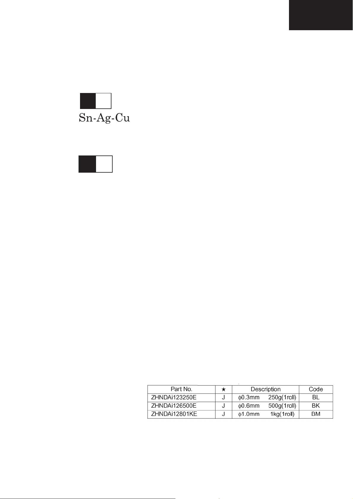
1 Employing lead-free solder
“ALL PWB” of this model employs lead-free solder. The LF symbol indicates lead-free solder, and is attached on the
PWBs and service manuals. The alphabetical character following LF shows the type of lead-free solder.
Example:
L Fa
Indicates lead-free solder of tin, silver and copper.
L F n
Sn-Ag-Ni
Indicates lead-free solder of tin, silver and nickel.
2 Using lead-free wire solder
When fi xing the PWB soldered with the lead-free solder, apply lead-free wire solder. Repairing with conventional lead
wire solder may cause damage or accident due to cracks.
As the melting point of lead-free solder (Sn-Ag-Cu) is higher than the lead wire solder by 40°C, we recommend you to
use a dedicated soldering bit, if you are not familiar with how to obtain lead-free wire solder or soldering bit, contact our
service station or service branch in your area.
3 Soldering
As the melting point of lead-free solder (Sn-Ag-Cu) is about 220°C which is higher than the conventional lead solder by
40°C, and as it has poor solder wettability, you may be apt to keep the soldering bit in contact with the PWB for extended
period of time. However, Since the land may be peeled off or the maximum heat-resistance temperature of parts may be
exceeded, remove the bit from the PWB as soon as you confi rm the steady soldering condition.
Lead-free solder contains more tin, and the end of the soldering bit may be easily corroded. Make sure to turn on and
off the power of the bit as required.
If a different type of solder stays on the tip of the soldering bit, it is alloyed with lead-free solder. Clean the bit after every
use of it.
When the tip of the soldering bit is blackened during use, fi le it with steel wool or fi ne sandpaper.
Be careful when replacing parts with polarity indication on the PWB silk.
Lead-free wire solder for servicing.
5
Page 6

LC-32LE631
LC-40LE631
LC-46LE631
END OF LIFE DISPOSAL
A. Information on Disposal for Users (private households)
1. In the European Union
Attention: If you want to dispose of this equipment, please do not use the ordinary dust bin!
Used electrical and electronic equipment must be treated separately and in accordance with legislation that requires
proper treatment, recovery and recycling of used electrical and electronic equipment.
Following the implementation by member states, private households within the EU states may return their used
Attention: Your product
is marked with this
symbol. It means that
used electrical and
electronic products
should not be mixed
with general household
waste. There is a
separate collection
system for these
products.
electrical and electronic equipment to designated collection facilities free of charge*. In some countries* your local
retailer may also take back your old product free of charge if you purchase a similar new one.
*) Please contact your local authority for further details.
If your used electrical or electronic equipment has batteries or accumulators, please dispose of these separately
beforehand according to local requirements.
By disposing of this product correctly you will help ensure that the waste undergoes the necessary treatment, recovery
and recycling and thus prevent potential negative effects on the environment and human health which could otherwise
arise due to inappropriate waste handling.
2. In other Countries outside the EU
If you wish to discard this product, please contact your local authorities and ask for the correct method of disposal.
For Switzerland: Used electrical or electronic equipment can be returned free of charge to the dealer, even if you don’t
purchase a new product. Further collection facilities are listed on the homepage of www.swico.ch or www.sens.ch.
B. Information on Disposal for Business Users
1. In the European Union
If the product is used for business purposes and you want to discard it:
Please contact your SHARP dealer who will inform you about the take-back of the product. You might be charged for
the costs arising from take-back and recycling. Small products (and small amounts) might be taken back by your local
collection facilities.
For Spain: Please contact the established collection system or your local authority for take-back of your used
products.
2. In other Countries outside the EU
If you wish to discard of this product, please contact your local authorities and ask for the correct method of disposal.
The battery supplied with this product contains traces of Lead.
For EU: The crossed-out wheeled bin implies that used batteries should not be put to the general household waste!
There is a separate collection system for used batteries, to allow proper treatment and recycling in accordance with
legislation. Please contact your local authority for details on the collection and recycling schemes.
For Switzerland: The used battery is to be returned to the selling point.
For other non-EU countries: Please contact your local authority for correct method of disposal of the used battery.
6
Page 7
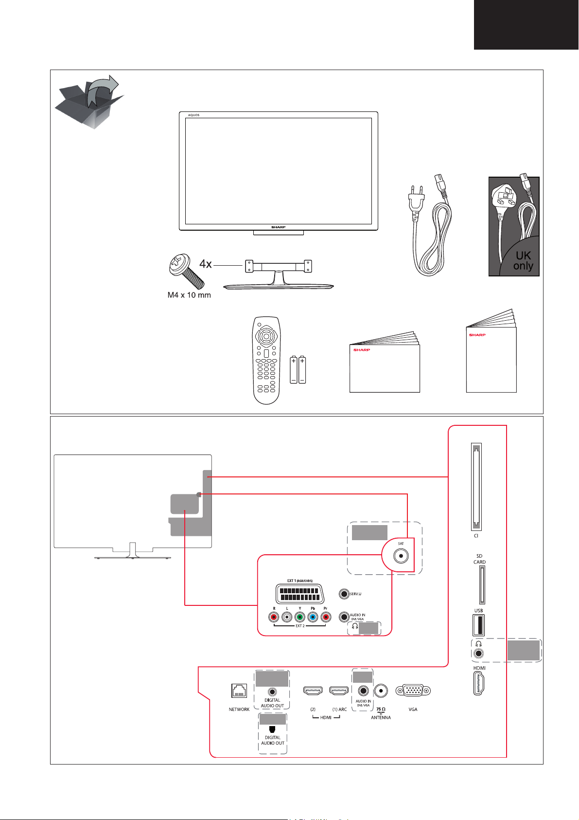
EN What’s in the box
DE Lieferumfang
FR Contenu de l’emballage
NL Wat zit er in de doos?
IT Contenuto della confezione
ES Contenido de la caja
PT Conteúdo da embalagem
DK Hvad er der i kassen
SV Förpackningens innehåll
NO Innholdet i esken
SU Toimituksen sisältö
GR ȆİȡȚİȤȩȝİȞĮ ıȣıțİȣĮıȓĮȢ
RU Ʉɨɦɩɥɟɤɬ ɩɨɫɬɚɜɤɢ
PL ZawartoĞü opakowania
HU A doboz tartalma
SK ýo je v balení?
CZ Obsah dodávky
TR Kutuda neler var
SI Kaj je v škatli
RO Ce se aÀ ă în cuti
ET Kasti sisu
LV KomplektƗcija
LT Kas yra rinkinyje
UK Ʉɨɦɩɥɟɤɬɚɰɿɹ ɭɩɚɤɨɜɤɢ
HR Što se nalazi u kutiji
LC-32LE631
LC-40LE631
LC-46LE631
OPERATION MANUAL
Information
Quick Start Guide
Only
LE/LU/LX630E
LE/LU/LX632E
Only
LE631E
(OPTICAL)
Only
LE/LU/LX632E
Only
LE631E
Only
LE/LU/LX630E
LE/LU/LX632E
Only
LE631E
7
Page 8
LC-32LE631
LC-40LE631
LC-46LE631
Operation Manual (Continued)
Only
LE/LU/LX630E
LE/LU/LX632E
VGA
Only
LE631E
(OPTICAL)
8
Page 9
Operation Manual (Continued)
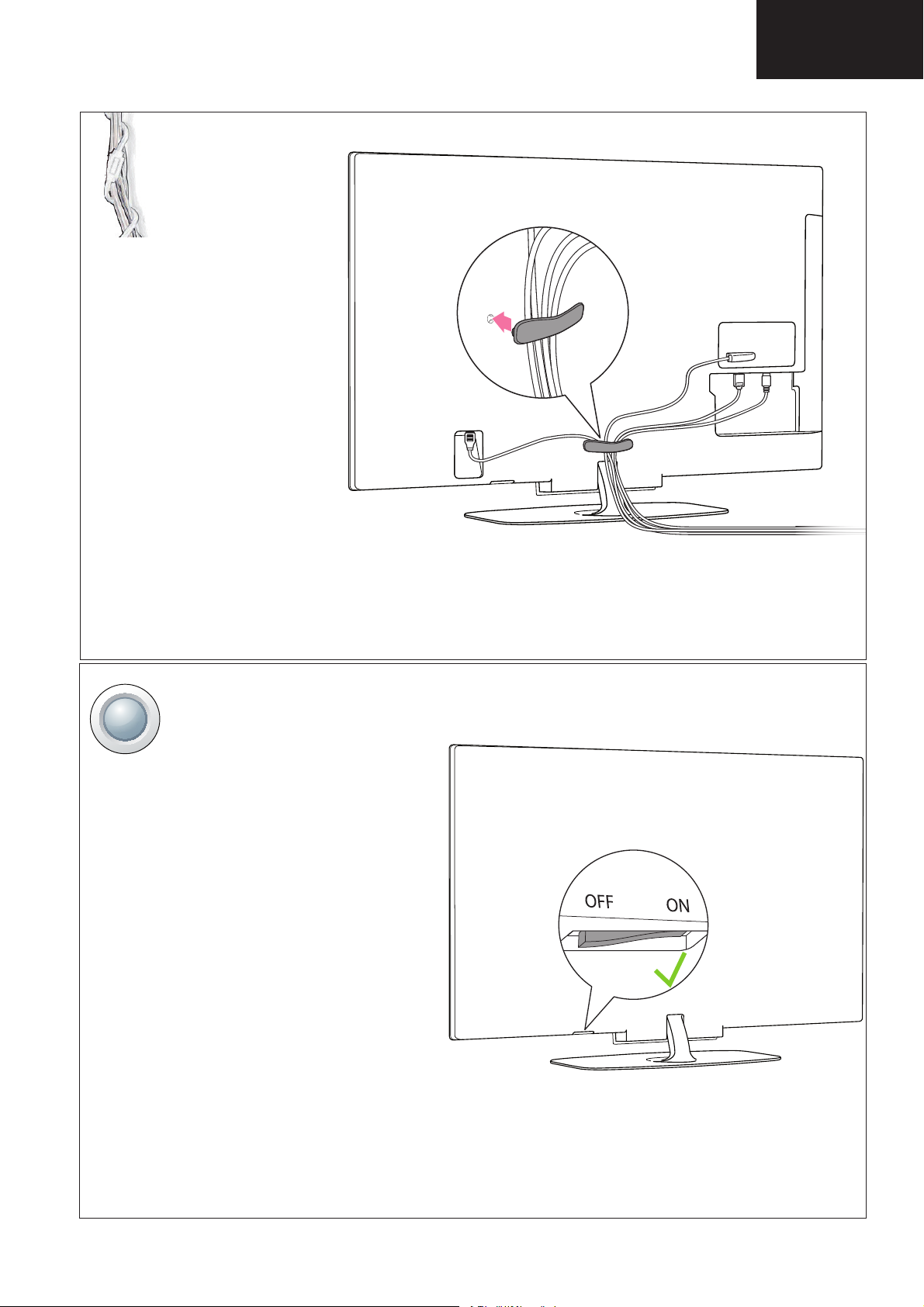
EN Manage cables
DE Kabel managen
FR Gestion des câbles
NL Kabels beheren
IT Gestione dei cavi
ES Manejo de los cables
PT Gerir os cabos
DK Håndter kabler
SV Hantera kablar
NO Ordne kablene
SU Kaapelien hallinta
GR ǻȚĮȤİȓȡȚıȘ țĮȜȦįȓȦȞ
RU ɍɫɬɚɧɨɜɤɚ ɤɚɛɟɥɟɣ
PL Ukáadanie przewodów
HU Kábelek elvezetése
SK Usporiadanie káblov
CZ Správa kabelĤ
TR KablolarÕ yönetme
SI Napeljite kable
RO Verif caĠi cablurile
ET Hallake kaableid
LV PieslƝdziet kabeƺus
LT Kabeliǐ jungimas
UK ɉɨɜɨɞɠɟɧɧɹ ɡ ɤɚɛɟɥɹɦɢ
HR Rukovanje kabelima
LC-32LE631
LC-40LE631
LC-46LE631
ON
EN Check that the power switch is on
DE Stellen Sie sicher, dass der Netzschalter eingeschaltet ist
FR Véri¿ ez que l’appreil est sous tension
NL Controleer of de schakelaar aan staat
IT Veri¿ care che l’intrruttore di alimentazione sia acceso
ES Comprobar que el interruptor de encendido está activado
PT Veri¿ car que o intrruptor está ligado
DK Kontroller, at tænd/sluk-knappen står på tænd
SV Kontrollera att strömbrytaren är på
NO Kontroller at av/på-knappen er på
SU Virtakytkimen asennon tarkistaminen
GR ǼȜȑȖȟIJİ İȐȞ İȓȞĮȚ İȞİȡȖȠʌȠȚȘȝȑȞȠȢ Ƞ įȚĮțȩʌIJȘȢ ȚıȤȪȠȢ
RU ɉɪɨɜɟɪɶɬɟ, ɜɤɥɸɱɟɧɚ ɥɢ ɤɧɨɩɤɚ ɩɢɬɚɧɢɹ
PL Zasilanie powinno byü wáączone
HU EllenĘrizze, hogy a készülék be van-e kapcsolva
SK Skontrolujte, þi je zapnutý hlavný vypínaþ
CZ Zkontrolujte, zda je zaĜízení zapnuto
TR Güç dü÷mesinin açÕk oldu÷undan emin olun
SI Preverite, ali je vklopno stikalo vklopljeno
RO Ve ri¿ caĠi dacă coutatorul este pornit
ET Kontrollige, kas toide on sisselülitatud
LV PƗrbaudiet, vai barošana ir ieslƝgta
LT Patikrinkite, ar Ƴjungtas maitinimo mygtukas
UK ɉɟɪɟɜɿɪ
HR Provjerite je li ukljuþen prekidaþ napajanja
ɬɟ, ɱɢ ɭɜɿɦɤɧɟɧɨ ɠɢɜɥɟɧɧɹ
9
Page 10
LC-32LE631
LC-40LE631
LC-46LE631
Operation Manual (Continued)
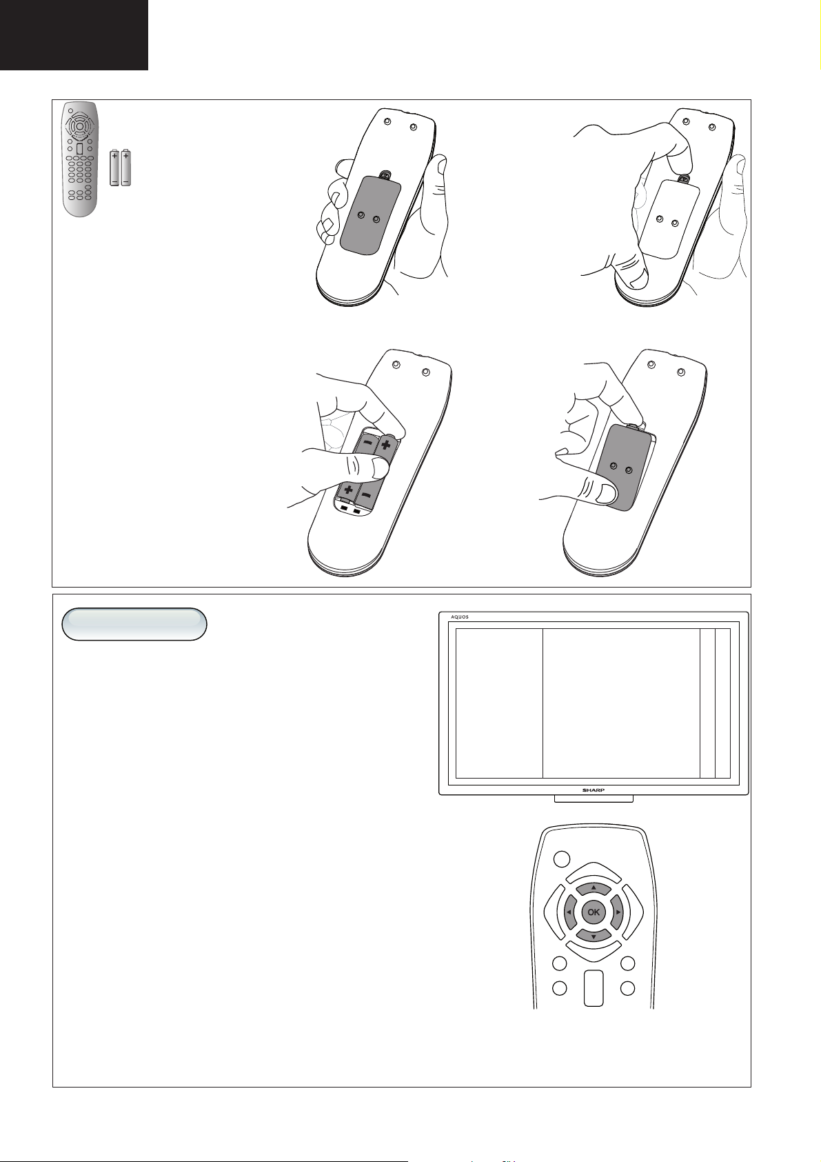
EN Insert batteries
DE Batterien einsetzen
FR Insertion des piles
NL Batterijen plaatsen
IT Inserimento delle batterie
ES Insertar pilas
PT Inserir baterias
DK Isæt batterier
SV Hantera kablar
NO Sett inn batteriene
SU Paristojen asettaminen paikoilleen
GR ǼȚıĮȖȦȖȒ ȝʌĮIJĮȡȚȫȞ
RU ɍɫɬɚɧɨɜɤɚ ɷɥɟɦɟɧɬɨɜ ɩɢɬɚɧɢɹ
PL Wkáadanie baterii
HU Elemek behelyezése
SK Vloženie batérií
CZ Vložte baterie
TR Pilleri takma
SI Vstavite baterije
RO IntroduceĠi bateriile
ET Sisestage patareid
LV Ievietojiet baterijas
LT Baterijǐ Ƴdơjimas
UK ȼɫɬɚɧɨɜɥɟɧɧɹ ɛɚɬɚɪɟɣ
HR Umetanje baterija
First Installation
EN Select your language and follow the onscreen instructions
DE Wählen Sie Ihre Sprache und folgen Sie den Anweisungen am Bildschirm
FR Sélectionnez votre langue et suivez les instructions à l’écran
NL Selecteer uw taal en volg de instructies op het scherm
IT Selezionare la lingua e seguire le istruzioni a video
ES Seleccione su idioma y siga las instrucciones en pantalla
PT Seleccionar o idioma e seguir as instruções no ecrã
DK Vælg sprog, og følg instruktionerne på skærmen
SV Kontrollera att strömbrytaren är på
NO Velg språk og følg instruksjonene på skjermen
SU Valitse kieli ja toimi näyttöön tulevien ohjeiden mukaan
GR ǼʌȚȜȑȟIJİ ȖȜȫııĮ țĮȚ ĮțȠȜȠȣșȒıIJİ IJȚȢ ȠįȘȖȓİȢ ʌȠȣ İȝijĮȞȓȗȠȞIJĮȚ ıIJȘȞ ȠșȩȞȘ
RU ȼɵɛɟɪɢɬɟ ɹɡɵɤ ɢ ɫɥɟɞɭɣɬɟ ɢɧɫɬɪɭɤɰɢɹɦ ɧɚ ɷɤɪɚɧɟ
PL Wybierz jĊzyk i postĊpuj zgodnie z instrukcjami wyĞwietlanymi na ekranie
HU Válassza ki a nyelvet, és kövesse a képernyĘn látható utasításokat
SK Vyberte jazyk a postupujte podĐa pokynov na obrazovke
CZ Vyberte jazyk a postupujte dle pokynĤ na obrazovce
TR Dili seçin ve ekrandaki talimatlarÕ uygulayÕn
SI Izberite jezik in sledite navodilom na zaslonu
RO SelectaĠi limba úi urmaĠi instrucĠiunile de pe ecran
ET Izaberite svoj jezik i sledite uputstva na ekranu
LV Atlasiet valodu un ievƝrojiet ekrƗnƗ redzamos norƗdƯjumus
Pasirinkite savo kalbą ir vykdykite instruk-cijas ekrane
LT
UK ȼɢɛɟɪɿɬɶ ɦɨɜɭ ɿ ɜɢɤɨɧɭɣɬɟ ɟɤɪɚɧɧɿ ɜɤɚɡɿɜɤɢ
HR Odaberite svoj jezik i slijedite upute na zaslonu
Please select your
language
English
Español
Français
Italiano
Nederlands
Deutsch
Dansk
►
▼
10
Page 11
Operation Manual (Continued)
LC-32LE631
LC-40LE631
LC-46LE631
11
Page 12
LC-32LE631
LC-40LE631
LC-46LE631
Operation Manual (Continued)
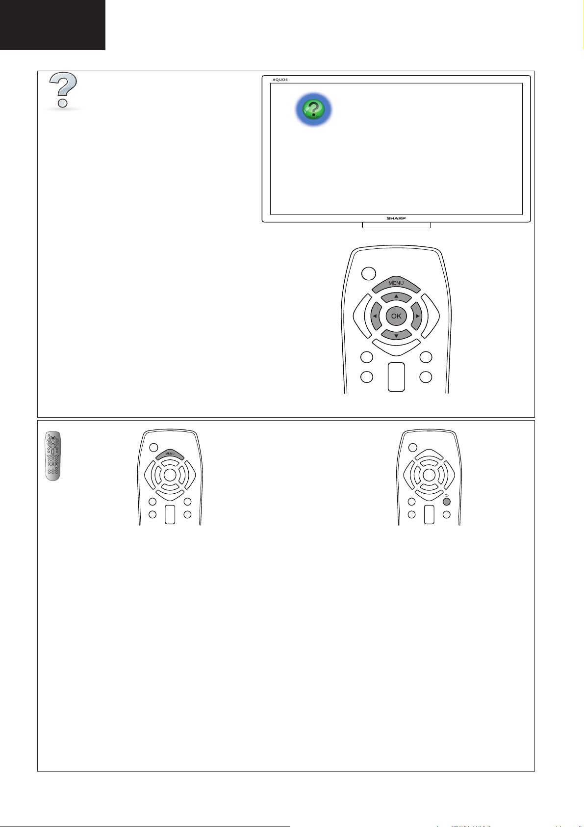
EN Onscreen help
DE Bildschirmhilfe
FR Aide à l’écran
NL Help op het scherm
IT Guida a video
ES Ayuda en pantalla
PT Ajuda no ecrã
DK Skærmhjælp
SV Hjälp på skärmen
NO Hjelp på skjermen
SU Näyttöohje
GR ǺȠȒșİȚĮ ıIJȘȞ ȠșȩȞȘ
RU ɗɥɟɤɬɪɨɧɧɚɹ ɫɩɪɚɜɤɚ
PL Pomoc wyĞwietlana na ekranie
HU KépernyĘsúgó
SK Pomocník na obrazovke
CZ NápovČda na obrazovce
TR Ekran yardÕmÕ
SI Zaslonska pomoþ
RO AsistenĠă pe ecran
ET Ekraanil kuvatav abi
LV PalƯdzƯba ekrƗnƗ
LT Pagalba ekrane
UK ȿɤɪɚɧɧɚ ɞɨɜɿɞɤɚ
HR Zaslonska pomoü
EN Menu
Menu screen on/off
DE Menü
Zum Anzeigen/Schließen des „Menü“
FR Menu
Marche/arrêt de l’écran du « Menu »
NL Menu
Menu scherm aan/uit
IT Menu
Schermata di Menu attivata /
disattvata
ES Menú
Activa/desactiva la pantalla del menú
PT Menu
Faz surgir/desaparecer o ecrã do
menu
DK Menu
Menu-skærm til/fra
SV Meny
In/urkoppling av meny-skärm
NO Meny
Meny-skjermbilde på/av
SU Valikko
Valikko-ruutu päälle tai pois päältä
GR ȂİȞȠȪ
ǼȞİȡȖȠʌȠȓȘıȘ / ǹʌİȞİȡȖȠʌȠȓȘıȘ IJȘȢ
ȠșȩȞȘȢ ȝİȞȠȪ.
RU Ɇɟɧɸ
ɥɸɱɟɧɢɟ/ɜɵɤɥɸɱɟɧɢɟ ɷɤɪɚɧɚ ɬɜ
ȼɤ
ɦɟɧɸ
PL Menu
WyĞwietla ekranu menu
HU Menü
A menü képernyĘ be- és kikapcsolá-
sára szolgál
SK Menu
Zobrazenie menu zapnuté/vypnuté.
CZ Menu
Zobrazení/skrytí menu
TR Menü
menü ekranÕnÕ açar/kapar
SI Meni
Prikaz zaslona meni
RO Meniu
A¿ úaĠi ecranul menu
ET Menüü
Menüü ekraan sisse/välja.
LV I zvƝlne
Loga izvƝlne atvƝršana/aizvƝršana.
LT Meniu
Meniu ekrano Ƴjungimas arba
išjungimas.
UK Ɇɟɧɸ
ɍɜɿɦɤɧɟɧɧɹ/ɜɢɦɤɧɟɧɧɹ ɟɤɪɚɧɭ
ɦɟɧɸ.
Izbornik
HR
Prikaži izbornik na zaslonu
12
EN Back
Return to the previous page
DE Zurück
Zurück zur vorherigen Seite
FR Retour
Retourner à la page précédente
NL Terug
Naar vorige pagina terugkeren
IT Precedente
Tornare alla pagina precedente
ES Retroceder
Volver a la página anterior
PT Voltar
Regressar à página anterior
DK Tilbage
Gå tilbage til forrige side
SV Tillbaka
Återgå till föregående sida
ilbake
NO T
Gå tilbake til forrige siden
SU Palaa
Palaa edelliselle sivulle
GR ȆȓıȦ
ǼʌȚıIJȡȠijȒ ıIJȘȞ ʌȡȠȘȖȠȪȝİȞȘ ıİȜȓįĮ
RU ɇɚɡɚɞ
ȼɨɡɜɪɚɬ ɤ ɩɪɟɞɵɞɭɳɟɣ ɫɬɪɚɧɢɰɟ
PL Wstecz
Wróü do poprzedniej strony
HU Vissza
Visszalépés az elĘzĘ oldalra
SK SpäĢ
Návrat na predchádzajúcu stranu
CZ ZpČt
Návrat na pĜedchozí stránku
TR Arka
Önceki sayfaya dönün
SI Nazaj
Vrnitev na prejšnjo stran
RO Înapoi
ReveniĠi la pagina anterioară
ET Tagasi
Tagasi eelmisele lehele
LV Atpakaƺ
Atgriezieties iepriekšƝjƗ lapƗ
LT A tgal
GrƳžimas Ƴ ankstesnƳ puslapƳ
UK ɇɚɡɚɞ
ɉɨɜɟɪɧɭɬɢɫɹ ɞɨ ɩɨɩɟɪɟɞɧɶɨʀ
ɫɬɨɪɿɧɤɢ
HR Prethodna
Povratak na prethodnu stranicu
Page 13
Operation Manual (Continued)
Ps Pr
LC-32LE631
LC-40LE631
LC-46LE631
EN Previous / Next
Switch channels or menu pages
DE Vorherige / Nächste Seite
Sender oder Menüseiten auswählen
FR Précédent / Suivant
Changer de chaîne ou pages du
menu
NL Vorige / Volgende
Door zender- of menupagina’s blade-
ren
IT Precedente / Successivo
Cambiare canale o pagina del menu
ES Anterior / Siguiente
Cambiar canales o páginas de menú
PT Anterior / Seguinte
Alternar canais ou páginas de menu
DK Forrige / Næste
Skift kanaler eller menusider
SV Föregående / Nästa
Byta kanaler eller menysidor
NO Forrige / Neste
Bytt kanal eller menyside
SU Edellinen / Seuraava
Vaihda kanavaa tai valikkosivua
GR ȆȡȠȘȖȠȪȝİȞȠ / ǼʌȩȝİȞȠ
ǼȞĮȜȜĮȖȒ țĮȞĮȜȚȫȞ Ȓ ıİȜȓįȦȞ ȝİȞȠȪ
ɡɚɞ / Ⱦɚɥɟɟ
RU ɇɚ
ɉɟɪɟɤɥɸɱɟɧɢɟ ɤɚɧɚɥɨɜ ɢɥɢ
ɫɬɪɚɧɢɰ ɦɟɧɸ
PL Poprzedni / NastĊpny
Przeáącz kanaáy albo strony menu
HU ElĘzĘ / KövetkezĘ
Csatornák vagy menüoldalak váltása
SK Predchádzajúce / Ćalšie
Prepínanie kanálov a stránok ponuky
CZ PĜedchozí / Další
PĜepínání kanálĤ nebo stránek
nabídky
TR Önceki / Sonraki
Kanal veya menü sayfasÕ de÷iútirin
SI Prejšnji / Naslednji
Preklapljanje kanalov ali strani v
meniju
RO Înapoi / Înainte
ComutaĠi canalele sau paginile de
meniu
ET Eelmine / Järgmine
Vahetage kanaleid või menüü lehti
LV LepriekšƝjais / NƗkamais
PƗrslƝdziet kanƗlus vai izvƝlnes lapas
LT Ankstesnis / kitas
Kanalǐ arba meniu puslapiǐ perjungi-
mas
UK ɇɚɡɚɞ / Ⱦɚɥɿ
ɉɟɪɟɦɢɤɚɧɧɹ ɤɚɧɚɥɿɜ ɱɢ ɫɬɨɪɿɧɨɤ
ɦɟɧɸ
HR Prethodno / Sljedeüe
Promjena kanala ili stranica
izbornika
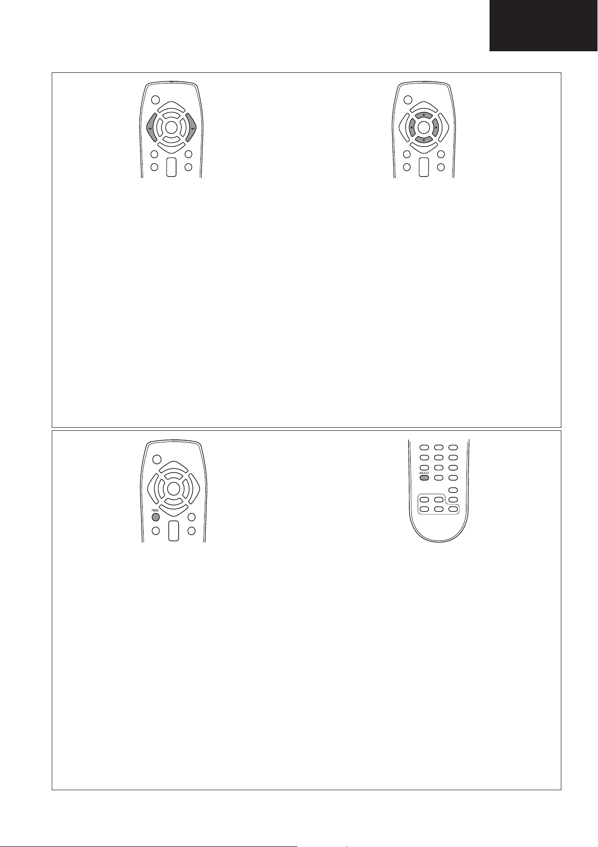
EN Navigation
Navigate menus or make selections
DE Navigationstasten
Durch Sender oder Menüseiten
navigieren
FR Touches de navigation
Parcourir les menus ou faire des
sélections
NL Navigatie
Door menu’s navigeren of selectie
maken
IT Navigazione
Sfogliare i menu o effettuare una
selezione
ES Navegación
Navegar por los menú o hacer selec-
ciones
PT Navegação
Navegar nos menus ou efectuar sele-
cções
DK Navigationsknapper
Naviger i menuer eller foretag valg
SV Navigering
Navigera i menyer eller göra val
NO Navigering
Naviger i menyer eller gjør valg
SU Siirtyminen
Siirry valikoissa tai tee valintoja
GR ȆȜȠȒȖȘıȘ
ȆİȡȚȒȖȘıȘ ıIJĮ ȝİȞȠȪ Ȓ țȐȞIJİ İʌȚȜȠȖȑȢ
RU ɇɚɜɢɝɚɰɢɹ
ɇɚɜɢɝɚɰɢɹ ɩɨ ɦɟɧɸ ɢɥɢ ɜɵɛɨɪ
ɭɫɬɚɧɨɜɨɤ
PL Nawigacja
Przeglądanie róĪnych menu albo
dokonywanie wyboru
HU Navigáció
Navigáció vagy kiválasztás a menü-
ben
SK Navigaþné tlaþidlo
Pohyb v ponukách alebo
uskutoþnenie výberu
CZ Ovládání
Procházení nabídek nebo volba
položek
TR Gezinme
Menülerde gezinin veya seçim yapÕn
SI Krmarjenje
Premikanje po menijih ali izbiranje
RO Navigare
NavigaĠi prin meniuri sau faceĠi selecĠii
ET Navigeerimine
Navigeerige menüüdes või tehke va-
likuid
LV NavigƗcija
PƗrvietojieties izvƝlnƝs vai atzƯmƝjiet
LT Naršymas
Meniu naršymas arba pasirinkimas
UK ɇɚɜɿɝɚɰɿɹ
ɇɚɜɿɝɚɰɿɹ ɦɟɧɸ ɚɛɨ ɜɢɛɿɪ
HR Navigacija
Pregled izbornika ili odabir
EN Find
Access channel list
DE Suchen
Senderliste aufrufen
FR Rechercher
Accéder à la liste des chaînes
NL Zoeken
Toegang tot lijst met zenders
IT Trova
Accesso all’elenco dei canali
ES Buscar
Acceder a la lista de canales
PT Localizar
Aceder à lista de canais
DK Find
Få adgang til kanalliste
SV Hitta
Få åtkomst till kanallista
NO Søk
Åpne kanallisten
SU Etsi
Avaa kanavaluettelo
GR ǼȪȡİıȘ
ȆȡȩıȕĮıȘ ıIJȠȞ țĮIJȐȜȠȖȠ țĮȞĮȜȚȫȞ
RU ɇɚɣɬɢ
Ⱦɨɫɬɭɩ ɤ ɫɩɢɫɤɭ ɤɚɧɚɥɨɜ
PL Znajd
Ĩ
DostĊp do listy kanaáów
HU Keresés
csatornalista megnyitása
A
SK Tlaþidlo vyhĐadávania
Prístup do zoznamu kanálov
CZ Vyhledat
ení seznamu kanálĤ
OtevĜ
TR Bul
Kanal listesine eriúin
SI Iskanje
Dostop do seznama kanalov
RO Găseúte
AccesaĠi lista de canale
ET Leia
Juurdepääs kanalite loendile
LV Atrast
Piekƺnjstiet kanƗlu sarakstam
LT Leškoti
Kanalǐ sąrašo prieiga
UK Ɂɧɚɣɬɢ
Ⱦɨɫɬɭɩ ɞɨ ɫɩɢɫɤɭ ɤɚɧɚɥɿɜ
HR Pronaÿi
Pristup popisu kanala
EN Adjust
Adjust TV settings
DE Anpassen
Fernsehereinstellungen anpassen
FR Régler
Régler les paramètres du téléviseur
NL Aanpassen
Tv-instellingen aanpassen
IT Regola
Regolare le impostazioni del
televisore
ES Ajustar
Ajustar con¿ guración del televisor
PT Ajustar
Ajustar de¿ nições de TV
DK Juster
Juster tv-indstillinger
SV Justera
Justera TV-inställningar
NO Juster
Juster TV-innstillinger
SU Säädä
Säädä television asetuksia
GR ȇȪșȝȚıȘ
ȆȡȠıĮȡȝȠȖȒ IJȦȞ ȡȣșȝȓıİȦȞ
IJȘȜİȩȡĮıȘȢ
13
RU ɇɚɫɬɪɨɣɤɚ
ɇɚɫɬɪɨɣɤɚ ɩɚɪɚɦɟɬɪɨɜ ɬɟɥɟɜɢɡɨɪɚ
PL Reguluj
Regulacja ustawieĔ telewizora
HU Beállítás
A TV beállításainak módosítása
SK Tlaþidlo úpravy
Úprava nastavení televízora
CZ Úprava
Úprava nastavení televizoru
TR Ayarla
TV ayarlarÕnÕ yapÕn
SI Prilagajanje
Prilagajanje nastavitev
TV-sprejemnika
RO Reglare
ReglaĠi setările televizorului
ET Reguleeri
Reguleerige teleri sätteid
LV P ielƗgot
PielƗgojiet TV iestatƯjumus
LT Reguliuoti
TV nustatymǐ regul-iavimas
UK ɇɚɥɚɲɬɭɜɚɬɢ
ɇɚɥɚɲɬɭɜɚɬɢ ɩɚɪɚɦɟɬɪɢ
ɬɟɥɟɦɨɜɥɟɧɧɹ
HR Podesi
Podešavanje postavki TV-a
Page 14
LC-32LE631
LC-40LE631
LC-46LE631
Operation Manual (Continued)
EN Source
Access connected devices
DE Quelle
Angeschlossene Geräte aufrufen
FR Source
Accéder aux périphériques connec-
tés
NL Bron
Toegang tot aangesloten apparaten
IT Sorgente
Accesso ai dispositivi collegati
ES Fuente
Acceder a dispositivos conectados
PT Origem
Aceder a dispositivos ligados
DK Kilde
Få adgang til tilsluttede enheder
SV Källa
Få åtkomst till anslutna enheter
Kilde
NO
KildeÅpne tilkoblede enheter
SU Lähde
Avaa liitetyt laitteet
GR ȆȘȖȒ
ȆȡȩıȕĮıȘ ıIJȚȢ ıȣȞįİįİȝȑȞİȢ
ıȣıțİȣȑȢ
RU ɂɫɬɨɱɧɢɤ
Ⱦɨɫɬɭɩ ɤ ɩɨɞɤɥɸɱɟɧɧɵɦ
ɭɫɬɪɨɣɫɬɜɚɦ
PL ħródáo
DostĊp do podáączonych urządzeĔ
HU Forrás
A csatlakoztatott készülékek elérése
SK Zdroj
Prístup k pripojeným zariadeniam
CZ Zdroj
OtevĜení nabídky pĜipojených
zaĜízení
TR Kaynak
Ba÷lÕ cihazlara eriúin
SI Vir
Dostop do prikljuþenih naprav
RO Sursă
AccesaĠi aparate conectate
ET Allikas
Juurdepääs ühendatud seadmetele
LV Avots
Piekƺnjstiet pievienotajƗm ierƯcƝm
LT Šaltinis
Prijungtǐ Ƴrenginiǐ prieiga
UK Ⱦɠɟɪɟɥɨ
Ⱦɨɫɬɭɩ ɞɨ ɩɿɞɤɥɸɱɟɧɢɯ ɩɪɢɫɬɪɨʀɜ
HR Izvor
Pristup prikljuþenim ureÿajima
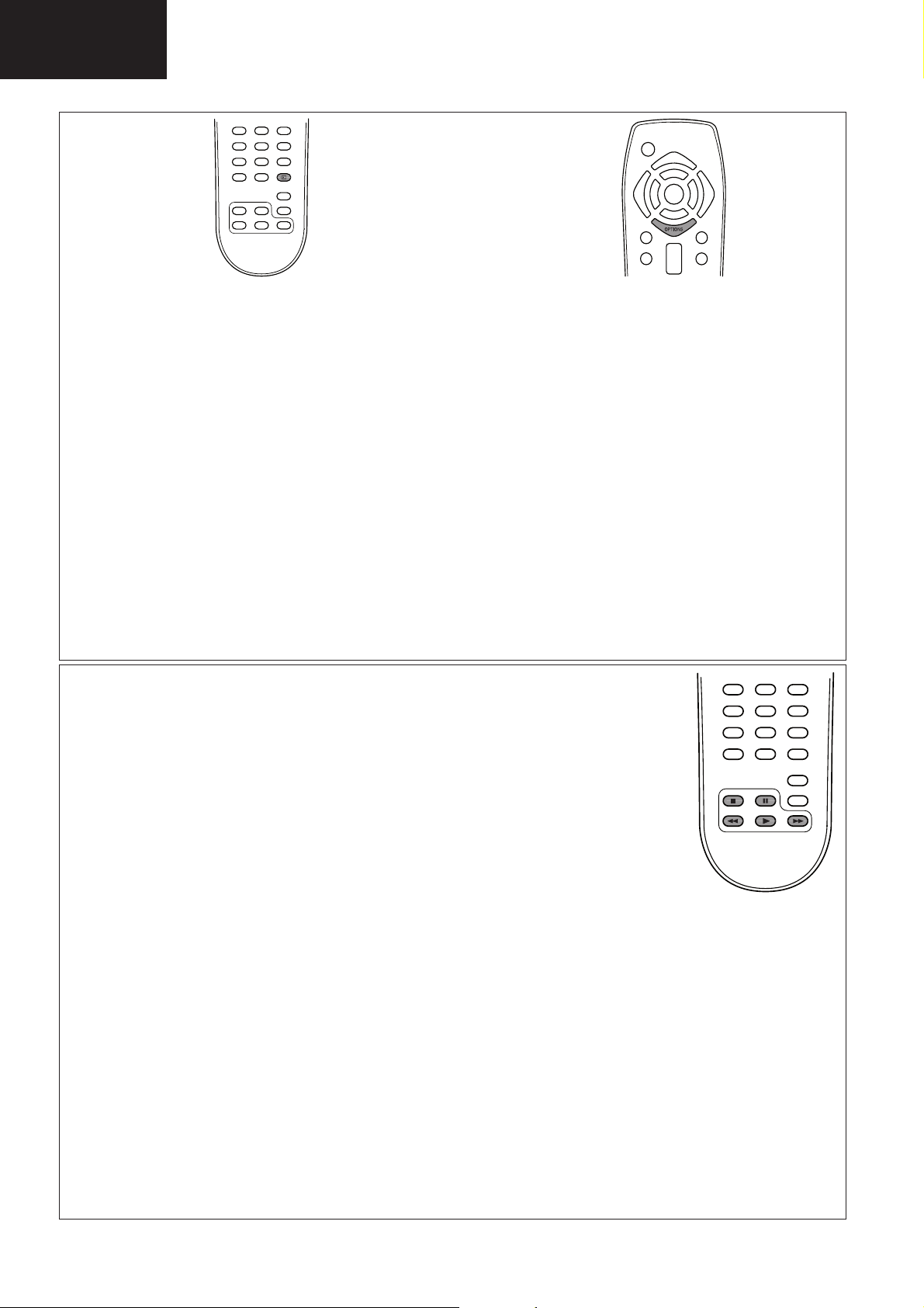
EN Options
Access TV options
DE Optionen
Fernseheroptionen aufrufen
FR Options
Accéder aux options du téléviseur
NL Opties
Toegang tot tv-opties
IT Opzioni
Accesso alle opzioni del televisore
ES Opciones
Acceder a opciones del televisor
PT Opções
Aceder a opções de TV
DK Indstillinger
Få adgang til tv-indstillinger
SV Alternativ
Få åtkomst till TV-alternativ
NO Alternativer
Åpne TV-alternativer
SU Asetukset
Avaa television asetukset
GR ǼʌȚȜȠȖȑȢ
ȆȡȩıȕĮıȘ ıIJȚȢ İʌȚȜȠȖȑȢ IJȘȜİȩȡĮıȘȢ
RU ɉɚɪɚɦɟɬɪɵ
Ⱦɨɫɬɭɩ ɤ ɩɚɪɚɦɟɬɪɚɦ ɬɟɥɟɜɢɡɨɪɚ
PL Opcje
DostĊp do opcji telewizora
HU LehetĘségek
A TV beállításainak elérése
SK Možnosti
Prístup k možnostiam televízora
CZ Možnosti
OtevĜení možností televizoru
TR Seçenekler
TV seçeneklerine eriúin
SI Možnosti
Dostop do možnosti TV-sprejemnika
RO OpĠiuni
AccesaĠi opĠiunile TV
ET Valikud
Juurdepääs teleri valikutele
LV Opcijas
Piekƺnjstiet TV opcijƗm
LT Parinktys
TV parinkþiǐ prieiga
UK ɉɚɪɚɦɟɬɪɢ
Ⱦɨɫɬɭɩ ɞɨ ɩɚɪɚɦɟɬɪɿɜ
ɬɟɥɟɦɨɜɥɟɧɧɹ
HR Opcije
Pristup TV opcijama
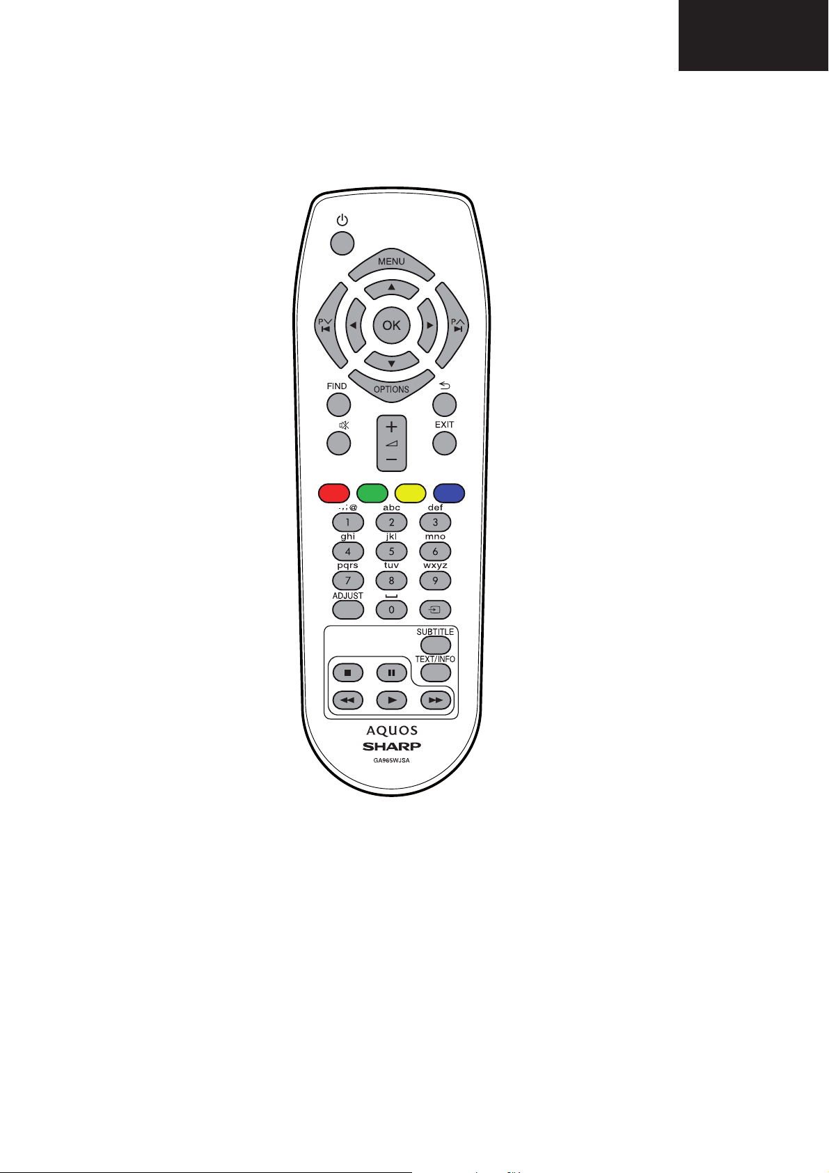
EN Play button
Control video or music play
DE Wiedergabetaste
Wiedergabe von Videos oder Musik
steuern
FR Touche de lecture
Contrôler la lecture de la vidéo ou de
la musique
NL Afspeelknop
Afspelen van muziek of video bedie-
nen
IT Pulsante di riproduzione
Controllare la riproduzi-one di video o
musica
ES Botón de reproducción
Controlar la reproducción de vídeo o
de música
PT Botão Reproduzir
Controlar vídeo ou reproduzir música
DK Afspilningsknap
Styr video eller musikafspilning
SV Uppspelningsknapp
Kontrollera video- eller musikuppspel-
ning
NO Spill
av-knapp
Kontroller video- eller musikkavspi-
lling
oista-painike
SU T
Hallitse videon tai musiikin toistoa
GR ȀȠȣȝʌȓ ĮȞĮʌĮȡĮȖȦȖȒȢ
DzȜİȖȤȠȢ ȕȓȞIJİȠ Ȓ ĮȞĮʌĮȡĮȖȦȖȒ
ȝȠȣıȚțȒȢ
RU Ʉɧɨɩɤɚ ɡɚɩɭɫɤɚ ɜɨɫɩɪɨɢɡɜɟɞɟɧɢɹ
ɍɩɪɚɜɥɟɧɢɟ ɜɨɫɩɪɨɢɡɜɟɞɟɧɢɟɦ ɜɢɞɟɨ
ɢɥɢ ɦɭɡɵɤɢ
PL Przycisk odtwarzania
Odtwarzanie ¿ lmów wideo lub muzyki
HU Lejátszás gomb
Videó vagy zene lejátszásának vezérlése
SK Tlaþidlo prehrávania
Ovládanie prehrávania videa alebo
hudby
CZ Tlaþítko PĜehrát
Ovládání pĜehrávání videa nebo hudby
TR Oynat dü÷mesi
Video veya müzi÷i kontrol edin
SI Tipka za predvajanje
Nadzor predvajanja videa ali glasbe
RO Buton redare
Control video sau redare muzică
ET Taasesitusnupp
Juhtige videote või muusika esitamist
LV Poga AtskaƼot
KontrolƝjiet video vai mnjzikas
atskaƼošanu
LT Leidimo mygtukas
Vaizdo Ƴrašo arba muzikos leidimo valdy-
mas
UK Ʉɧɨɩɤɚ ɜɿɞɬɜɨɪɟɧɧɹ
Ʉɟɪɭɜɚɧɧɹ ɜɿɞɬɜɨɪɟɧɧɹɦ ɜɿɞɟɨ ɱɢ
ɦɭɡɢɤɢ
HR Tipka Play
Upravljanje videom ili sviranje glazbe
14
Page 15
Operation Manual (Continued)
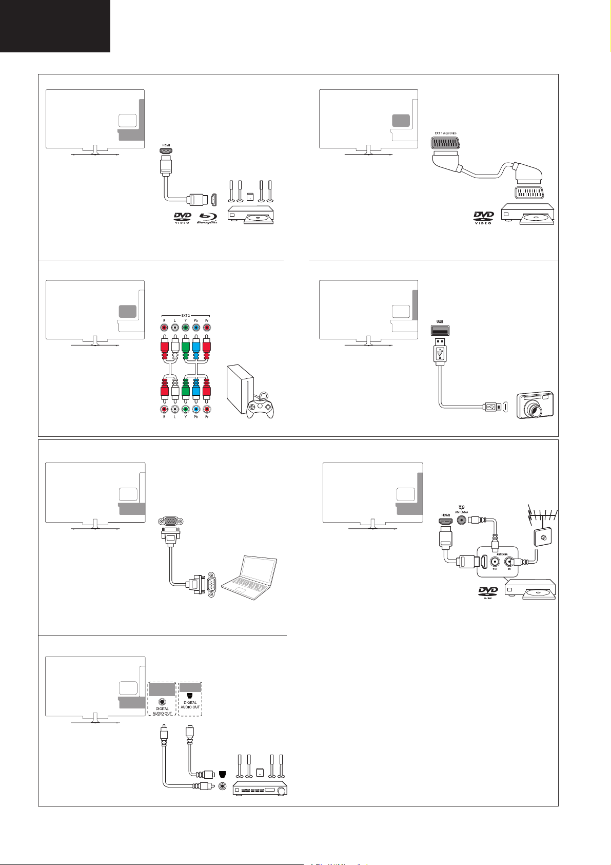
Connect devices
LC-32LE631
LC-40LE631
LC-46LE631
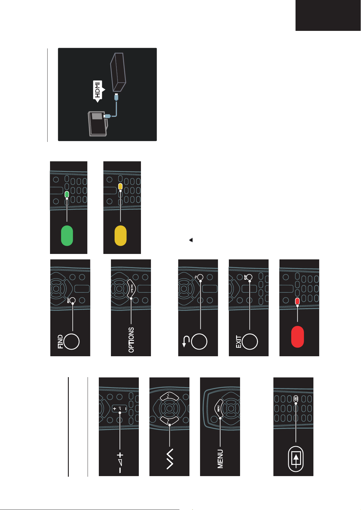
For the best picture and sound quality,
connect a DVD, Blu-ray disc player, or game
console through HDMI (TM).
To watch a device, add it to the TV menu.
1. Press MENU > [Add your devices].
2. Follow the onscreen instructions.
Note: If you are prompted to select the TV
connection, select the connector that this
device uses. See Connect your TV >
Connect devices (Page 33) for information
on connection.
If a Link operation or HDMI-Consumer
Electronic Control (HDMI-CEC) compliant
device is connected to the TV, it is
automatically added to the TV menu when
both devices are switched on.
To watch a connected device
1. Press MENU.
2. Select the newly added device icon.
to select the next TV tour.
To select a green menu option or to access
energy efficient settings.
To select a yellow menu option or to access
the electronic user manual.
Read more about the remote control in Use
your TV > Controls > Remote control
(Page 10).
Alternatively, look at the index in Search
for...
Press
1 Get started
To open or close the Find menu.
In the Find menu, access the channel list.
TV tour
Remote control
To open or close the Options menu.
Options menus offer convenient settings for
TV channels or programmes.
To adjust the volume.
To switch TV channels.
To return to the previous menu page.
To open or close the Menu.
In the Menu, access connected devices,
To exit from a menu or function.
To select a red menu option or watch TV
demonstration clips.
picture and sound settings, and other useful
features.
To open or close the Source menu.
In the Source menu, access connected
devices.
15
Page 16
LC-32LE631
LC-40LE631
LC-46LE631
REVISION LIST
1. Revision List
First Edition
Manual :xxxxxxxxxxxx
TECHNICAL SPECIFICATIONS, DIVERSITY AND CONNECTIONS
2. Technical Specifi cations, Diversity and Connections
Index of this chapter:
2.1 Technical Specifications
2.1 Technical Specifications
2.2 Directions for Use
2.3 Connections
2.4 Chassis Overview
Notes:
For on-line product support please use the CTN links in Table
2-1. Here is product information available, as well as getting
started, user manuals, frequently asked questions and
software & drivers.
• Figures can deviate due to the different set executions.
• Specifications are indicative (subject to change).
Table 2-1 Described Model Numbers and Diversity
SSB 2 4 7 9 10
PWB
CTN
LC-32L*631E Page Page Page Page Page Page Page Page Page Page Page Page Page Page Page Page Page Page
LC-40L*631E Page Page Page Page Page Page Page Page Page Page Page Page Page Page Page Page Page Page
LC-46L*631E Page Page Page Page Page Page Page Page Page Page Page Page Page Page Page Page Page Page
Cabinet & Mechanical Parts
3139 123 xxxxx
Mechanics Descript.
Conection Overview
Wiring Dressing
Assembly Removal
LCD Removal
PSU
B01 Tuner
Schematics
Wiring Diagram
B02 (PNX85500)
B03 (DC/ / Class D)
B04 (I / O)
B05 (DDR)
B06 (DDR)
B08 (DVBS-Supp.)
B09 (non-DVBS-conn.)
E (IR/LED/key Board)
B10 (DVBT2)
2.2 Directions for Use
You can download this information from the SHARP’s Global Intranet site:
http://www.global.sharp.co.jp/
(Click on e-Service.)
16
Page 17
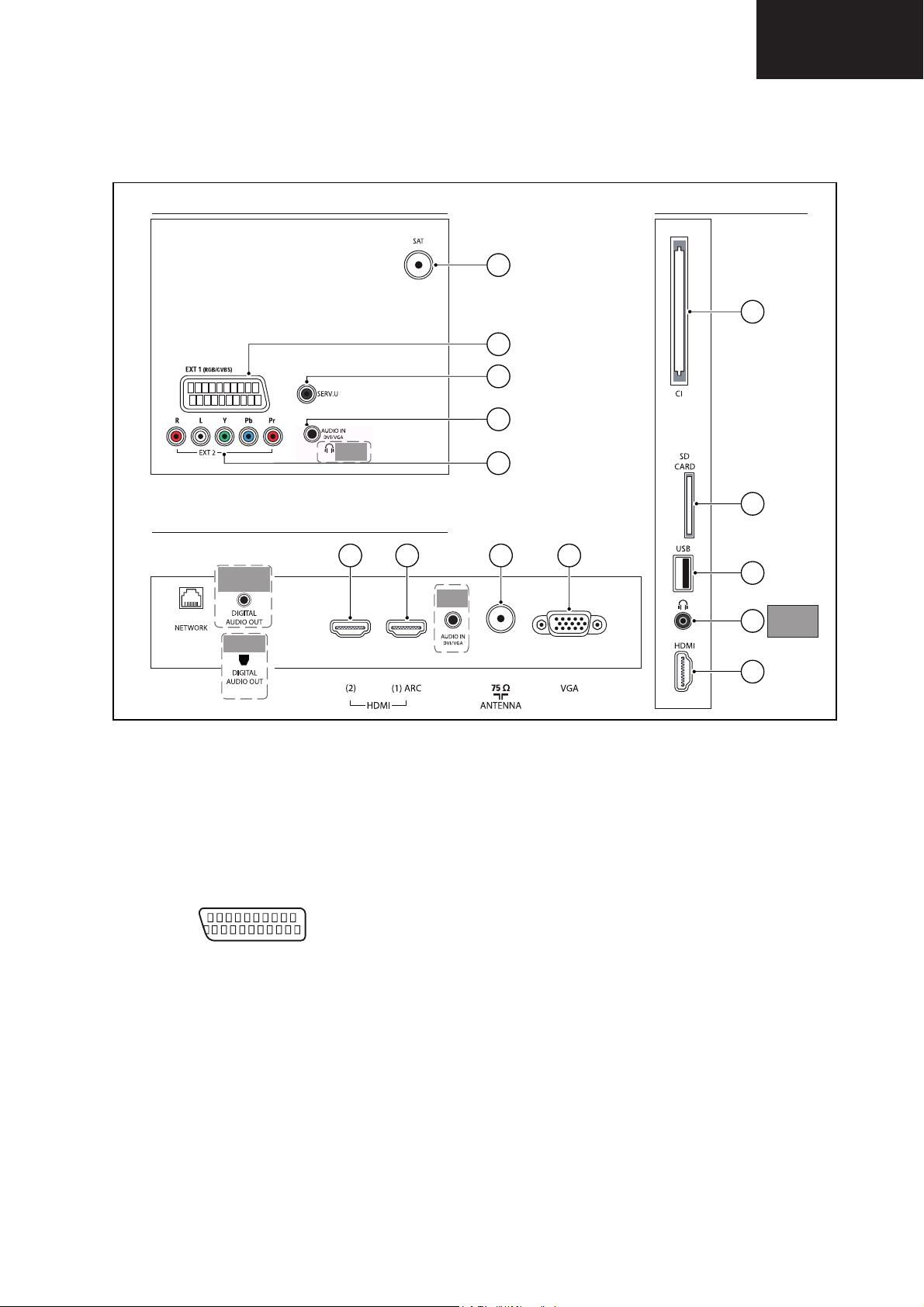
REAR CONNECTORS
BOTTOM REAR CONNECTORS
SIDE CONNECTORS
19100_043_110214.eps
110216
12
5
3
4
2
1
13
14
15
16
6 7 8 9 10 11
Technical Specifi cation, Diversity and Connections (continued)
2.3 Connections
Only
LE631E
LC-32LE631
LC-40LE631
LC-46LE631
Only
LE/LU/LX630E
LE/LU/LX632E
Only
LE631E
(OPTICAL)
Note: The following connector colour abbreviations are used
(acc. to DIN/IEC 757): Bk= Black, Bu= Blue, Gn= Green, Gy=
Grey, Rd= Red, Wh= White, Ye= Yellow.
2.3.1 Rear Connections
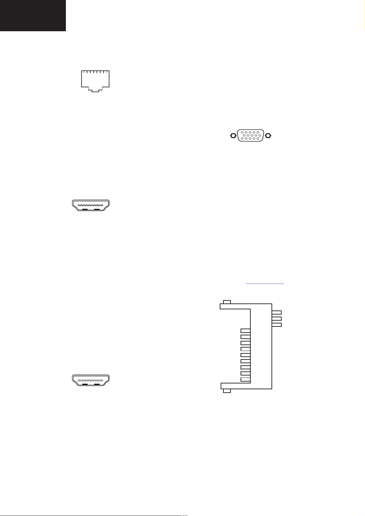
1 - EXT1: Video RGB - In, CVBS - In/Out, Audio - In/Out
20
21
10000_001_090121.eps
Figure 2-2 SCART connector
1 - Audio R 0.5 V
2 - Audio R 0.5 V
3 - Audio L 0.5 V
4 - Ground Audio Gnd H
5 - Ground Blue Gnd H
6 - Audio L 0.5 V
7 - Video Blue 0.7 V
8 - Function Select 0 - 2 V: INT
4.5 - 7 V: EXT 16:9
9.5 - 12 V: EXT 4:3 j
9 - Ground Green Gnd H
10 - n.c.
11 - Video Green 0.7 V
12 - n.c.
2
1
090121
/ 1 kohm k
RMS
/ 10 kohm j
RMS
/ 1 kohm k
RMS
/ 10 kohm j
RMS
/ 75 ohm jk
PP
/ 75 ohm j
PP
Only
LE631E
Figure 2-1 Connection overview
13 - Ground Red Gnd H
14 - Ground P50 Gnd H
15 - Video Red 0.7 V
16 - Status/FBL 0 - 0.4 V: INT
17 - Ground Video Gnd H
18 - Ground FBL Gnd H
19 - Video CVBS/Y 1 V
20 - Video CVBS 1 V
21 - Shield Gnd H
2 - Service Connector (UART)
1 - Ground Gnd H
2 - UART_TX Transmit k
3 - UART_RX Receive j
3 - EXT2: Cinch: Video YPbPr - In, Audio - In
Gn - Video Y 1 V
Bu - Video Pb 0.7 V
Rd - Video Pr 0.7 V
Rd - Audio - R 0.5 V
Wh - Audio - L 0.5 V
4 - Cinch: Audio - In (VGA/DVI)
Rd - Audio R 0.5 V
Wh - Audio L 0.5 V
5 - SAT - In
- - F-type Coax, 75 ohm D
17
/ 75 ohm j
PP
1 - 3 V: EXT / 75 ohm j
/ 75 ohm k
PP
/ 75 ohm j
PP
/ 75 ohm jq
PP
/ 75 ohm jq
PP
/ 75 ohm jq
PP
RMS
RMS
RMS
RMS
Only
LE/LU/LX630E
LE/LU/LX632E
/ 10 kohm jq
/ 10 kohm jq
/ 10 kohm jq
/ 10 kohm jq
Page 18
LC-32LE631
112345678
10000_025_090121.eps
090121
10000_017_090121.eps
090428
19
1
18 2
10000_017_090121.eps
090428
19
1
18 2
1
6
10
11
5
15
10000_002_090121.eps
090127
10000_049_100210.eps
100210
10
11
12
CD
GND
WP
14
GND
13
GND
1
2
3
4
5
6
7
8
9
DAT3/CS
CMD/DI
GND1
VDD
CLOCK
GND2
DAT0/D0
DAT1/IRQ
DAT2/NC
LC-40LE631
LC-46LE631
Technical Specifi cation, Diversity and Connections (continued)
2.3.2 Rear Connections - Bottom
6 - RJ45: Ethernet
Figure 2-3 Ethernet connector
1 - TD+ Transmit signal k
2 - TD- Transmit signal k
3 - RD+ Receive signal j
4 - CT Centre Tap: DC level fixation
5 - CT Centre Tap: DC level fixation
6 - RD- Receive signal j
7 - GND Gnd H
8 - GND Gnd H
7 - Cinch: S/PDIF - Out
Bk - Coaxial 0.4 - 0.6V
/ 75 ohm kq
PP
8 - HDMI 2: Digital Video, Digital Audio - In
Figure 2-4 HDMI (type A) connector
1 - D2+ Data channel j
2 - Shield Gnd H
3 - D2- Data channel j
4 - D1+ Data channel j
5 - Shield Gnd H
6 - D1- Data channel j
7 - D0+ Data channel j
8 - Shield Gnd H
9 - D0- Data channel j
10 - CLK+ Data channel j
11 - Shield Gnd H
12 - CLK- Data channel j
13 - Easylink/CEC Control channel jk
14 - n.c.
15 - DDC_SCL DDC clock j
16 - DDC_SDA DDC data jk
17 - Ground Gnd H
18 - +5V j
19 - HPD Hot Plug Detect j
20 - Ground Gnd H
13 - Easylink/CEC Control channel jk
14 - ARC Audio Return Channel k
15 - DDC_SCL DDC clock j
16 - DDC_SDA DDC data jk
17 - Ground Gnd H
18 - +5V j
19 - HPD Hot Plug Detect j
20 - Ground Gnd H
10 - Aerial - In
- - IEC-type (EU) Coax, 75 ohm D
11 - VGA: Video RGB - In
Figure 2-6 VGA Connector
1 - Video Red 0.7 V
2 - Video Green 0.7 V
3 - Video Blue 0.7 V
4-n.c.
/ 75 ohm j
PP
/ 75 ohm j
PP
/ 75 ohm j
PP
5 - Ground Gnd H
6 - Ground Red Gnd H
7 - Ground Green Gnd H
8 - Ground Blue Gnd H
9-+5V
10 - Ground Sync Gnd H
+5 V j
DC
11 - n.c.
12 - DDC_SDA DDC data j
13 - H-sync 0 - 5 V j
14 - V-sync 0 - 5 V j
15 - DDC_SCL DDC clock j
2.3.3 Side Connections
12 - Common Interface
68p - See diagram B01A Common Interface
jk
13 - SD-Card: Secure Digital Card - In/Out (optional)
9 - HDMI 1: Digital Video - In, Digital Audio with ARC - In/
Out
Figure 2-5 HDMI (type A) connector
1 - D2+ Data channel j
2 - Shield Gnd H
3 - D2- Data channel j
4 - D1+ Data channel j
5 - Shield Gnd H
6 - D1- Data channel j
7 - D0+ Data channel j
8 - Shield Gnd H
9 - D0- Data channel j
10 - CLK+ Data channel j
11 - Shield Gnd H
12 - CLK- Data channel j
Figure 2-7 SD-Card connector
1 - DAT3/CS Signal jk
2 - CMD/DI Signal k
3 - GND1 Gnd H
4 - Vdd Supply k
5 - CLOCK Signal k
6 - GND2 Gnd H
7 - DAT0/D0 Signal jk
8 - DAT1/IRQ Signal jk
9 - DAT2/NC Signal jk
10 - CD Signal j
11 - GND Gnd H
18
Page 19

1 2 3 4
10000_022_090121.eps
090121
Technical Specifi cation, Diversity and Connections (continued)
LC-32LE631
LC-40LE631
LC-46LE631
12 -WP Signal j
13 -GND Gnd H
14 -GND Gnd H
14 - USB2.0
Figure 2-8 USB (type A)
2.4 Chassis Overview
Refer to chapter Block Diagrams for PWB/CBA locations.
1-+5V k
2 - Data (-) jk
3 - Data (+) jk
4 - Ground Gnd H
15 - Head phone (Output)
Bk - Head phone 32 - 600 ohm / 10 mW ot
16 - HDMI : Digital Video, Digital Audio - In
See 8 - HDMI 2: Digital Video, Digital Audio - In
19
Page 20

LC-32LE631
LC-40LE631
LC-46LE631
PRECAUTIONS, NOTES AND ABBREVIATION LIST
3. Precautions, Notes and Abbreviation List
Index of this chapter:
3.1 Safety Instructions
3.2 Warnings
3.3 Notes
3.4 Abbreviation List
3.1 Safety Instructions
Safety regulations require the following during a repair:
• Connect the set to the Mains/AC Power via an isolation
transformer (> 800 VA).
• Replace safety components, indicated by the symbol h,
only by components identical to the original ones. Any
other component substitution (other than original type) may
increase risk of fire or electrical shock hazard.
Safety regulations require that after a repair, the set must be
returned in its original condition. Pay in particular attention to
the following points:
• Route the wire trees correctly and fix them with the
mounted cable clamps.
• Check the insulation of the Mains/AC Power lead for
external damage.
• Check the strain relief of the Mains/AC Power cord for
proper function.
• Check the electrical DC resistance between the Mains/AC
Power plug and the secondary side (only for sets that have
a Mains/AC Power isolated power supply):
1. Unplug the Mains/AC Power cord and connect a wire
between the two pins of the Mains/AC Power plug.
2. Set the Mains/AC Power switch to the “on” position
(keep the Mains/AC Power cord unplugged!).
3. Measure the resistance value between the pins of the
Mains/AC Power plug and the metal shielding of the
tuner or the aerial connection on the set. The reading
should be between 4.5 M: and 12 M:.
4. Switch “off” the set, and remove the wire between the
two pins of the Mains/AC Power plug.
• Check the cabinet for defects, to prevent touching of any
inner parts by the customer.
3.2 Warnings
• All ICs and many other semiconductors are susceptible to
electrostatic discharges (ESD w). Careless handling
during repair can reduce life drastically. Make sure that,
during repair, you are connected with the same potential as
the mass of the set by a wristband with resistance. Keep
components and tools also at this same potential.
• Be careful during measurements in the high voltage
section.
• Never replace modules or other components while the unit
is switched “on”.
• When you align the set, use plastic rather than metal tools.
This will prevent any short circuits and the danger of a
circuit becoming unstable.
• Where necessary, measure the waveforms and voltages
with (D) and without (E) aerial signal. Measure the
voltages in the power supply section both in normal
operation (G) and in stand-by (F). These values are
indicated by means of the appropriate symbols.
3.3.2 Schematic Notes
• All resistor values are in ohms, and the value multiplier is
often used to indicate the decimal point location (e.g. 2K2
indicates 2.2 k:).
• Resistor values with no multiplier may be indicated with
either an “E” or an “R” (e.g. 220E or 220R indicates 220 :).
• All capacitor values are given in micro-farads (P u10
nano-farads (n u10
• Capacitor values may also use the value multiplier as the
decimal point indication (e.g. 2p2 indicates 2.2 pF).
• An “asterisk” (*) indicates component usage varies. Refer
to the diversity tables for the correct values.
3.3.3 Spare Parts
For the latest spare part overview, consult the Spare Part at the
end of this document.
3.3.5 Lead-free Soldering
Due to lead-free technology some rules have to be respected
by the workshop during a repair:
• Use only lead-free soldering tin. If lead-free solder paste is
required, please contact the manufacturer of your soldering
equipment. In general, use of solder paste within
workshops should be avoided because paste is not easy to
store and to handle.
• Use only adequate solder tools applicable for lead-free
soldering tin. The solder tool must be able:
– To reach a solder-tip temperature of at least 400°C.
– To stabilize the adjusted temperature at the solder-tip.
– To exchange solder-tips for different applications.
• Adjust your solder tool so that a temperature of around
360°C - 380°C is reached and stabilized at the solder joint.
Heating time of the solder-joint should not exceed ~ 4 sec.
Avoid temperatures above 400°C, otherwise wear-out of
tips will increase drastically and flux-fluid will be destroyed.
To avoid wear-out of tips, switch “off” unused equipment or
reduce heat.
● Mix of lead-free soldering tin/parts with leaded soldering tin/
parts is possible but SHARP recommends strongly to avoid
mixed regimes. If this cannot be avoided, carefully clear the
solder-joint from old tin and re-solder with new tin.
-9
), or pico-farads (p u10
-6
),
-12
).
3.3 Notes
3.3.1 General
• Measure the voltages and waveforms with regard to the
chassis (= tuner) ground (H), or hot ground (I), depending
on the tested area of circuitry. The voltages and waveforms
shown in the diagrams are indicative. Measure them in the
Service Default Mode with a colour bar signal and stereo
sound (L: 3 kHz, R: 1 kHz unless stated otherwise) and
picture carrier at 475.25 MHz for PAL, or 61.25 MHz for
NTSC (channel 3).
20
Page 21

Precautions, Notes and Abrreviattion List (continued)
p
p
LC-32LE631
LC-40LE631
LC-46LE631
3.3.7 Board Level Repair (BLR) or Component Level Repair
(CLR)
If a board is defective, consult your repair procedure to decide
if the board has to be exchanged or if it should be repaired on
component level.
If your repair procedure says the board should be exchanged
completely, do not solder on the defective board. Otherwise, it
cannot be returned to the O.E.M. supplier for back charging!
3.3.8 Practical Service Precautions
• It makes sense to avoid exposure to electrical shock.
While some sources are expected to have a possible
dangerous impact, others of quite high potential are of
limited current and are sometimes held in less regard.
• Always respect voltages. While some may not be
dangerous in themselves, they can cause unexpected
reactions that are best avoided. Before reaching into a
powered TV set, it is best to test the high voltage insulation.
It is easy to do, and is a good service precaution.
3.4 Abbreviation List
0/6/12 SCART switch control signal on A/V
AARA Automatic Aspect Ratio Adaptation:
ACI Automatic Channel Installation:
ADC Analogue to Digital Converter
AFC Automatic Frequency Control: control
AGC Automatic Gain Control: algorithm that
AM Amplitude Modulation
AP Asia Pacific
AR Aspect Ratio: 4 by 3 or 16 by 9
ASF Auto Screen Fit: algorithm that adapts
ATSC Advanced Television Systems
ATV See Auto TV
Auto TV A hardware and software control
AV External Audio Video
AVC Audio Video Controller
AVIP Audio Video Input Processor
B/G Monochrome TV system. Sound
BDS Business Display Solutions (iTV)
BLR Board-Level Repair
BTSC Broadcast Television Standard
B-TXT Blue TeleteXT
C Centre channel (audio)
CEC Consumer Electronics Control bus:
CL Constant Level: audio output to
CLR Com
board. 0 = loop through (AUX to TV),
6 = play 16 : 9 format, 12 = play 4 : 3
format
algorithm that adapts aspect ratio to
remove horizontal black bars; keeps
the original aspect ratio
algorithm that installs TV channels
directly from a cable network by
means of a predefined TXT page
signal used to tune to the correct
frequency
controls the video input of the feature
box
aspect ratio to remove horizontal black
bars without discarding video
information
Committee, the digital TV standard in
the USA
system that measures picture content,
and adapts image parameters in a
dynamic way
carrier distance is 5.5 MHz
Committee. Multiplex FM stereo sound
system, originating from the USA and
used e.g. in LATAM and AP-NTSC
countries
remote control bus on HDMI
connections
connect with an external amplifier
onent Level Repair
CP Connected Planet / Copy Protection
CSM Customer Service Mode
CTI Color Transient Improvement:
CVBS Composite Video Blanking and
DAC Digital to Analogue Converter
DBE Dynamic Bass Enhancement: extra
DCM Data Communication Module. Also
DDC See “E-DDC”
D/K Monochrome TV system. Sound
DFI Dynamic Frame Insertion
manipulates steepness of chroma
transients
Synchronization
low frequency amplification
referred to as System Card or
Smartcard (for iTV).
carrier distance is 6.5 MHz
21
Page 22

LC-32LE631
LC-40LE631
LC-46LE631
Precautions, Notes and Abrreviattion List (continued)
DFU Directions For Use: owner's manual
DMR Digital Media Reader: card reader
DMSD Digital Multi Standard Decoding
DNM Digital Natural Motion
DNR Digital Noise Reduction: noise
DRAM Dynamic RAM
DRM Digital Rights Management
DSP Digital Signal Processing
DST Dealer Service Tool: special remote
DTCP Digital Transmission Content
DVB-C Digital Video Broadcast - Cable
DVB-T Digital Video Broadcast - Terrestrial
DVD Digital Versatile Disc
DVI(-d) Digital Visual Interface (d= digital only)
E-DDC Enhanced Display Data Channel
EDID Extended Display Identification Data
EEPROM Electrically Erasable and
EMI Electro Magnetic Interference
EPG Electronic Program Guide
EPLD Erasable Programmable Logic Device
EU Europe
EXT EXTernal (source), entering the set by
FDS Full Dual Screen (same as FDW)
FDW Full Dual Window (same as FDS)
FLASH FLASH memory
FM Field Memory or Frequency
FPGA Field-Programmable Gate Array
FTV Flat TeleVision
Gb/s Giga bits per second
G-TXT Green TeleteXT
H H_sync to the module
HD High Definition
HDD Hard Disk Drive
HDCP High-bandwidth Digital Content
HDMI High Definition Multimedia Interface
HP HeadPhone
I Monochrome TV system. Sound
2
I
C Inter IC bus
2
D Inter IC Data bus
I
2
S Inter IC Sound bus
I
IF Intermediate Frequency
IR Infra Red
IRQ Interrupt Request
ITU-656 The ITU Radio communication Sector
reduction feature of the set
control designed for service
technicians
Protection; A protocol for protecting
digital audio/video content that is
traversing a high speed serial bus,
such as IEEE-1394
(VESA standard for communication
channel and display). Using E-DDC,
the video source can read the EDID
information form the display.
(VESA standard)
Programmable Read Only Memory
SCART or by cinches (jacks)
Modulation
Protection: A “key” encoded into the
HDMI/DVI signal that prevents video
data piracy. If a source is HDCP coded
and connected via HDMI/DVI without
the proper HDCP decoding, the
picture is put into a “snow vision” mode
or changed to a low resolution. For
normal content distribution the source
and the display device must be
enabled for HDCP “software key”
decoding.
carrier distance is 6.0 MHz
(ITU-R) is a standards body
subcommittee of the International
Telecommunication Union relating to
radio communication. ITU-656 (a.k.a.
SDI), is a digitized video format used
for broadcast grade video.
Uncompressed digital component or
digital composite signals can be used.
The SDI signal is self-synchronizing,
uses 8 bit or 10 bit data words, and has
a maximum data rate of 270 Mbit/s,
with a minimum bandwidth of 135
MHz.
ITV Institutional TeleVision; TV sets for
hotels, hospitals etc.
LS Last Status; The settings last chosen
by the customer and read and stored
in RAM or in the NVM. They are called
at start-up of the set to configure it
according to the customer's
preferences
LATAM Latin America
LCD Liquid Crystal Display
LED Light Emitting Diode
L/L' Monochrome TV system. Sound
carrier distance is 6.5 MHz. L' is Band
I, L is all bands except for Band I
LS Loudspeaker
LVDS Low Voltage Differential Signalling
Mbps Mega bits per second
M/N Monochrome TV system. Sound
carrier distance is 4.5 MHz
MHEG Part of a set of international standards
related to the presentation of
multimedia information, standardised
by the Multimedia and Hypermedia
Experts Group. It is commonly used as
a language to describe interactive
television services
MIPS Microprocessor without Interlocked
Pipeline-Stages; A RISC-based
microprocessor
MOP Matrix Output Processor
MOSFET Metal Oxide Silicon Field Effect
Transistor, switching device
MPEG Motion Pictures Experts Group
MPIF Multi Platform InterFace
MUTE MUTE Line
MTV Mainstream TV: TV-mode with
Consumer TV features enabled (iTV)
NC Not Connected
NICAM Near Instantaneous Compounded
Audio Multiplexing. This is a digital
sound system, mainly used in Europe.
NTC Negative Temperature Coefficient,
non-linear resistor
NTSC National Television Standard
Committee. Color system mainly used
in North America and Japan. Color
carrier NTSC M/N= 3.579545 MHz,
NTSC 4.43= 4.433619 MHz (this is a
VCR norm, it is not transmitted off-air)
NVM Non-Volatile Memory: IC containing
TV related data such as alignments
O/C Open Circuit
OSD On Screen Display
OAD Over the Air Download. Method of
software upgrade via RF transmission.
Upgrade software is broadcasted in
TS with TV channels.
OTC On screen display Teletext and
Control; also called Artistic (SAA5800)
P50 Project 50: communication protocol
between TV and peripherals
PAL Phase Alternating Line. Color system
mainly used in West Europe (color
carrier= 4.433619 MHz) and South
America (color carrier PAL M=
22
Page 23

Precautions, Notes and Abrreviattion List (continued)
LC-32LE631
LC-40LE631
LC-46LE631
3.575612 MHz and PAL N= 3.582056
PCB Printed Circuit Board (same as “PWB”)
PCM Pulse Code Modulation
PDP Plasma Display Panel
PFC Power Factor Corrector (or Pre-
PIP Picture In Picture
PLL Phase Locked Loop. Used for e.g.
POD Point Of Deployment: a removable
POR Power On Reset, signal to reset the uP
PSDL Power Supply for Direct view LED
PSL Power Supply with integrated LED
PSLS Power Supply with integrated LED
PTC Positive Temperature Coefficient,
PWB Printed Wiring Board (same as “PCB”)
PWM Pulse Width Modulation
QRC Quasi Resonant Converter
QTNR Quality Temporal Noise Reduction
QVCP Quality Video Composition Processor
RAM Random Access Memory
RGB Red, Green, and Blue. The primary
RC Remote Control
RC5 / RC6 Signal protocol from the remote
RESET RESET signal
ROM Read Only Memory
RSDS Reduced Swing Differential Signalling
R-TXT Red TeleteXT
SAM Service Alignment Mode
S/C Short Circuit
SCART Syndicat des Constructeurs
SCL Serial Clock I
SCL-F CLock Signal on Fast I
SD Standard Definition
SDA Serial Data I
SDA-F DAta Signal on Fast I
SDI Serial Digital Interface, see “ITU-656”
SDRAM Synchronous DRAM
SECAM SEequence Couleur Avec Mémoire.
SIF Sound Intermediate Frequency
SMPS Switched Mode Power Supply
SoC System on Chip
SOG Sync On Green
SOPS Self Oscillating Power Supply
SPI Serial Peripheral Interface bus; a 4-
S/PDIF Sony Philips Digital InterFace
SRAM Static RAM
SRP Service Reference Protocol
SSB Small Signal Board
SSC Spread Spectrum Clocking, used to
STB Set Top Box
STBY STand-BY
SVGA 800 × 600 (4:3)
MHz)
conditioner)
FST tuning systems. The customer
can give directly the desired frequency
CAM module, implementing the CA
system for a host (e.g. a TV-set)
backlight with 2D-dimming
drivers
drivers with added Scanning
functionality
non-linear resistor
color signals for TV. By mixing levels
of R, G, and B, all colors (Y/C) are
reproduced.
control receiver
data interface
d'Appareils Radiorécepteurs et
Téléviseurs
Color system mainly used in France
and East Europe. Color carriers=
4.406250 MHz and 4.250000 MHz
wire synchronous serial data link
standard
reduce the effects of EMI
2
C
2
C bus
2
C
2
C bus
SVHS Super Video Home System
SW Software
SWAN Spatial temporal Weighted Averaging
Noise reduction
SXGA 1280 × 1024
TFT Thin Film Transistor
THD Total Harmonic Distortion
TMDS Transmission Minimized Differential
Signalling
TS Transport Stream
TXT TeleteXT
TXT-DW Dual Window with TeleteXT
UI User Interface
uP Microprocessor
UXGA 1600 × 1 200 (4:3)
V V-sync to the module
VESA Video Electronics Standards
Association
VGA 640 × 480 (4:3)
VL Variable Level out: processed audio
output toward external amplifier
VSB Vestigial Side Band; modulation
method
WYSIWYR What You See Is What You Record:
record selection that follows main
picture and sound
WXGA 1 280 × 768 (15:9)
XTAL Quartz crystal
XGA 1024 × 768 (4:3)
Y Luminance signal
Y/C Luminance (Y) and Chrominance (C)
signal
YPbPr Component video. Luminance and
scaled color difference signals (B-Y
and R-Y)
YUV Component video
23
Page 24
LC-32LE631
LC-40LE631
LC-46LE631
4. Mechanical Instructions
Index of this chapter:
4.1 Cable Dressing LC-xx631E series Styling
4.2 Service Positions
4.3 Assy/Panel Removal Sundance Styling (LC-xxLE631E series)
4.4 Set Re-assembly
4.5 Dimensions 32”
4.6 Dimensions 40”
4.7 Dymensions 46”
4.8 Removing of Major Parts 32”
4.9 Removing of Major Parts 40” & 46”
Notes:
• Figures below can deviate slightly from the actual situation,
due to the different set executions.
MECHANICAL INSTRUCTIONS
4.1 Cable Dressing LC-xx631E series Styling
10 tapes (80 mm)
2 tapes (150 mm)
2 conductive tapes (40 mm)
1 x 11 mm clamp
Figure 4-1 Cable dressing LC-32LE631 Series
24
Page 25
Mechanical Instructions (continued)
LC-32LE631
LC-40LE631
LC-46LE631
5 tapes (80 mm)
3 tapes (150 mm)
Figure 4-2 Cable dressing LC-40/46LE631 series
4.2 Service Positions
For easy servicing of a TV set, the set should be put face down
on a soft flat surface, foam buffers or other specific workshop
tools. Ensure that a stable situation is created to perform
measurements and alignments. When using foam bars take
care that these always support the cabinet and never only the
display. Caution: Failure to follow these guidelines can
seriously damage the display!
Ensure that ESD safe measures are taken.
4.3 Assy/Panel Removal Sundance Styling
(LC-xxLE631E series)
The instructions in this section also apply to the LCxxLE631E series.
For the 40” and 46” sets, additional instructions (rear cover
removal) apply. Refer to subsection Additional instructions
for 40/46LE631E and Removing of Major Parts.
The instructions apply to the 32LE631E.
2 conductive tapes (40 mm)
2 x 11 mm clamp
1. Remove all screws of the rear cover.
2. Lift the rear cover from the TV. Make sure that wires and
flat coils are not damaged while lifting the rear cover from
the set.
Additional instructions for 40/46LE631E sets have a dedicated method to open the bottom catches when removing
the rear cover.
Refer to Figure 4-4
1 1
1 x 17 mm clamp
1 ferrite core
and Figure 4-5 for details.
19100_04 8_110216.ep s
110315
4.3.1 Rear Cover
Warning: Disconnect the mains power cord before you remove
the rear cover.
Note: it is not necessary to remove the stand while removing
the rear cover.
Figure 4-4 Bottom catches 40” and 46” sets -1-
25
Page 26
LC-32LE631
19100_050_110216.eps
110216
1
1
1
22
2
2
19100_051_110216.eps
110216
1
2
2
2
2
2
2
1
LC-40LE631
LC-46LE631
Mechanical Instructions (continued)
2
19100_049_110216.ep s
Figure 4-5 Bottom catches 40” and 46” sets -2-
It is advised to lay the set with front facing down before
executing this operation.
1. Remove all screws from the rear cover.
2. Use a round rod (diameter 2 mm) and insert it in one of the
holes [1].
3. Push the catch located inside the rear cover away by
inserting the rod [2] through the hole and lifting the rear
cover at the same time.
4. Repeat the same procedure on the other hole.
4.3.2 Speakers
Tweeters
Each tweeter unit is mounted with one screw.
When defective, replace the whole unit.
Subwoofer
The central subwoofer is located in the centre of the set and is
secured by two bosses.
When defective, replace the whole unit.
4.3.3 Mains Switch
Refer to Figure 4-6
for details.
110315
Figure 4-7 Main Power Supply
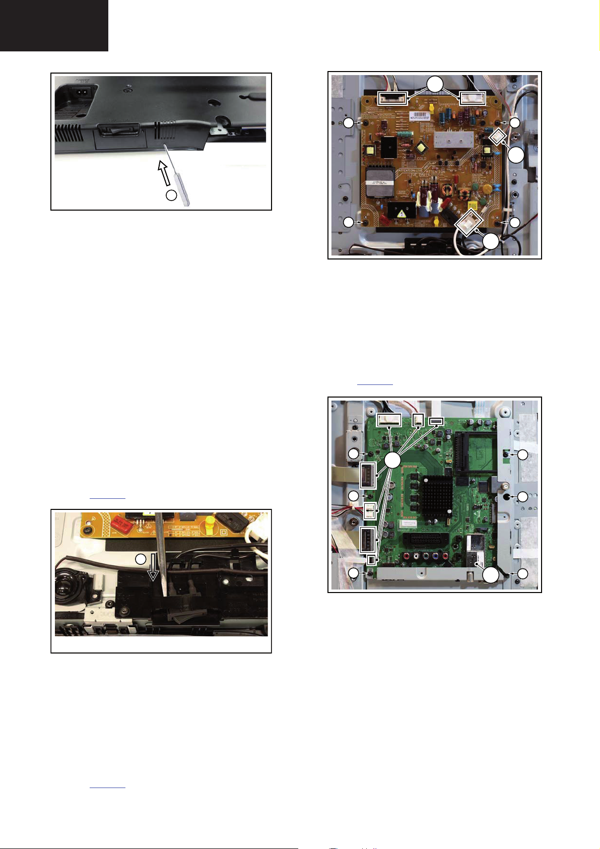
1. Unplug all connectors [1].
2. Remove the fixation screws [2].
3. Take the board out.
When defective, replace the whole unit.
4.3.5 Small Signal Board (SSB)
Refer to Figure 4-8
for details.
4.3.4 Main Power Supply
The mains switch is mounted on a plastic subframe and can be
removed without removing the subframe.
1. Use a screwdriver and push the switch out of its casing [1].
2. Unplug the connectors [2].
When defective, replace the whole unit.
Refer to Figure 4-7
1
Figure 4-6 Mains switch
for details.
19100_047_110216.eps
110315
Figure 4-8 SSB
1. Unplug all connectors [1].
2. Remove the fixation screws [2].
3. Take the board out.
When remounting, ensure that the side shielding [3] is
positioned correctly.
26
Page 27
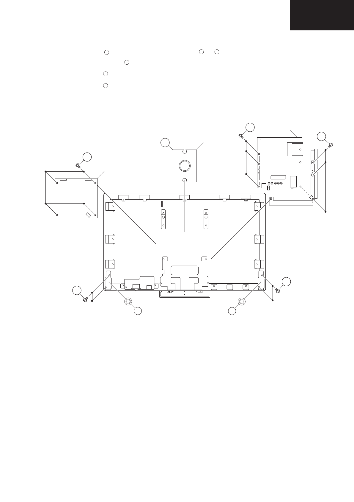
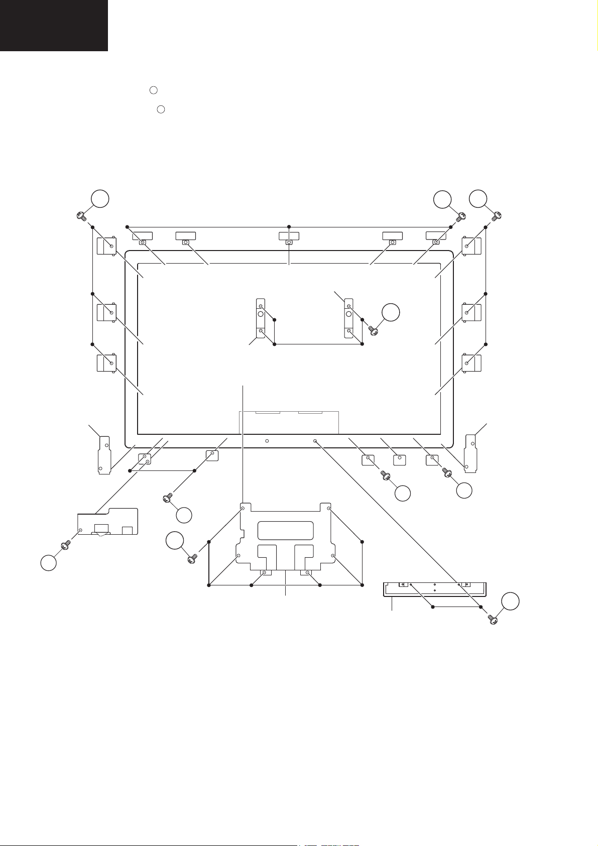
4.3.7 Removing of major Parts 32”
[]
LC-32LE631
LC-40LE631
LC-46LE631
1. Remove the 4 lock screws and detach the Stand.
2. Remove the 4 screw hole plugs .
3. Remove the 4 lock screws , 1 lock screw , 1 lock screw , 6 lock screws and detach the Rear Cabinet.
Rear
1
2
3
4
5
6
3
Cabinet
5
6
4
1
2
3
Stand
Front Cabinet
27
Page 28
LC-32LE631
MAIN UNIT
POWER UNIT
LC-40LE631
LC-46LE631
4.3.7 Removing of major Parts 32” (Continued)
4. Disconnect all the connectors from all the PWBs.
SPEAKER -R
(TWEETER)
TO DISPLAY
SUPPLY
[1316] [1M95]
[1308]
MAIN
SWITCH
INLET
SPEAKER
(SUBWOOFER)
[1M95]
[1G50]
[1D38]
[1735]
[1G51]
[1M19]
SPEAKER -L
(TWEETER)
28
Page 29
4.3.7 Removing of major Parts 32” (Continued)
5. Remove the 4 lock screws and detach the SPEAKER (tweeters) (R) , (L) .
6. Remove the SPEAKER (subwoofer) ,
7
10
LC-32LE631
LC-40LE631
LC-46LE631
9
8
7. Remove the 4 lock screws , and detach the POWER unit.
8. Remove the 6 lock screws and detach the TERMINAL COVER side, bottom and the MAIN unit.
11
12
12
10
SPEAKER
(subwoofer)
11
POWER unit
TERMINAL
COVER
side
MAIN unit
12
TERMINAL
COVER
bottom
7
7
SPEAKER -R
(tweeter)
8
9
SPEAKER -L
(tweeter)
29
Page 30
LC-32LE631
LC-40LE631
LC-46LE631
4.3.7 Removing of major Parts 32” (Continued)
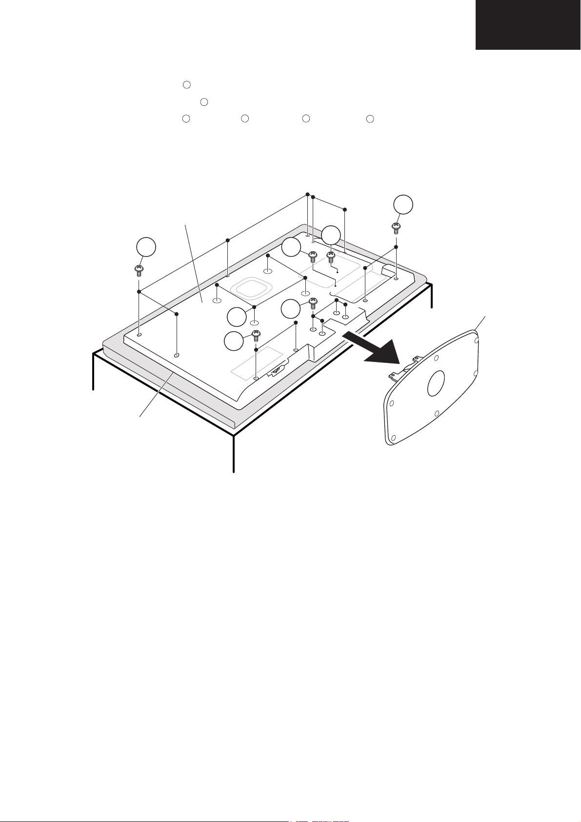
9. Remove the 8 lock screws and detach the STAND bracket and the CONTROL BUTTON unit.
10. Remove the 18 lock screws and detach the PANEL brackets top/side and bottom, VESA brackets and TWEETER brackets.
14
13
14
PANEL
bracket
14
14
(top)
PANEL
bracket
(side)
14
PANEL
bracket
(side)
VESA
bracket
TWEETER
bracket
14
13
14
PANEL
bracket
(bottom)
STAND
bracket
14
CONTROL
BUTTON
unit
PANEL
bracket
(bottom)
TWEETER
bracket
14
13
30
Page 31

4.3.7 Removing of major Parts 32” (Continued)
LC-32LE631
LC-40LE631
LC-46LE631
11. Detach the PANEL .
15
15
31
Page 32

LC-32LE631
LC-40LE631
LC-46LE631
4.3.8 Removing of major Parts 40”
1. Remove the 4 lock screws and detach the Stand.
2. Remove the 4 screw hole plugs .
3. Remov e the 14 lock screws , 1 lock screw and detach the Rear Cabinet.
1
2
3
4
Rear
Cabinet
2
3
3
4
1
Stand
Front Cabinet
32
Page 33

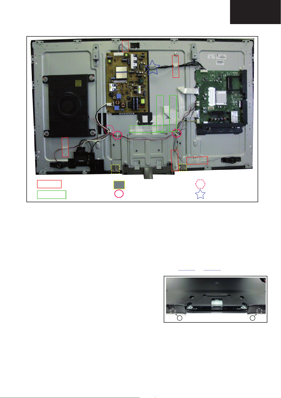
4.3.8 Removing of major Parts 40” (Continued)
MAIN UNIT
POWER UNIT
4. Disconnect all the connectors from all the PWBs.
TO DISPLAY
SUPPLY
[1316]
[1M99]
SPEAKER
(SUBWOOFER)
[1308]
LC-32LE631
LC-40LE631
LC-46LE631
[1M95]
[1G50]
[1D38]
[1735]
[1G51]
SPEAKER -R
(TWEETER)
MAIN
SWITCH
[1M19]
INLET
SPEAKER -L
(TWEETER)
33
Page 34

LC-32LE631
LC-40LE631
LC-46LE631
4.3.8 Removing of major Parts 40” (Continued)
5. Remove the SPEAKER (subwoofer) .
6. Remove the 2 lock screws and detach the POWER SWITCH and INLET HOLDER BRACKET .
7. Remove the 3 lock screws , and detach the SPEAKER (tweeter) R and SPEAKER (tweeter) L .
8. Remove the 6 lock screws and detach the TERMINAL COVER side, bottom and the MAIN unit.
9. Remove the 4 lock screws and detach the POWER UNIT.
6
8
11
12
5
7
9 10
12
POWER unit
11
5
SPEAKER
(subwoofer)
MAIN unit
TERMINAL
COVER
side
11
SPEAKER -R
(tweeter)
8
6
TERMINAL
COVER
bottom
9
SPEAKER -L
(tweeter)
10
POWER SWITCH
AND INLET HOLDER
BRACKET
7
8
34
Page 35

4.3.8 Removing of major Parts 40” (Continued)
10. Remove the 6 PANEL brackets top, 8 PANEL brackets side and 4 PANEL brackets bottom.
LC-32LE631
LC-40LE631
LC-46LE631
11. Remove the 4 lock screws and detach the Vesa brackets top.
12. Remove the 6 lock screws and detach the STAND bracket.
13. Remove the 2 lock screws and detach the CONTROL BUTTON.
13
14
15
PANEL bracket (top)
13
PANEL
bracket
(side)
VESA
bracket (top)
PANEL
bracket
(side)
PANEL bracket (bottom)
14
STAND
bracket
15
CONTROL
BUTTON
unit
35
Page 36

LC-32LE631
LC-40LE631
LC-46LE631
4.3.8 Removing of major Parts 40” (Continued)
14. Detach the PANEL .
16
16
36
Page 37

4.3.9 Removing of major Parts 46”
LC-32LE631
LC-40LE631
LC-46LE631
1. Remove the 4 lock screws and detach the Stand.
2. Remove the 4 screw hole plugs .
3. Remove the 14 lock screws , 1 lock screw and detach the Rear Cabinet.
1
2
3
4
Rear
Cabinet
2
3
3
4
1
Stand
Front Cabinet
37
Page 38

LC-32LE631
MAIN UNIT
POWER UNIT
LC-40LE631
LC-46LE631
4.3.9 Removing of major Parts 46” (Continued)
4. Disconnect all the connectors from all the PWBs.
TO DISPLAY
SUPPLY
[1316]
[1M99]
SPEAKER
(SUBWOOFER)
[1308]
[1M95]
[1G50]
[1D38]
[1735]
[1G51]
SPEAKER -R
(TWEETER)
MAIN
SWITCH
[1M19]
INLET
SPEAKER -L
(TWEETER)
38
Page 39

4.3.9 Removing of major Parts 46” (Continued)
LC-32LE631
LC-40LE631
LC-46LE631
5. Remove the SPEAKER (subwoofer) .
6. Remove the 2 lock screws and detach the POWER SWITCH and INLET HOLDER BRACKET .
7. Remove the 3 lock screws , and detach the SPEAKER (tweeter) R and SPEAKER (tweeter) L .
8. Remove the 6 lock screws and detach the TERMINAL COVER side, bottom and the MAIN unit.
9. Remove the 4 lock screws and detach the POWER UNIT.
6
8
11
12
5
7
9 10
12
POWER unit
11
5
SPEAKER
(subwoofer)
MAIN unit
TERMINAL
COVER
side
11
SPEAKER -R
(tweeter)
8
6
TERMINAL
COVER
bottom
9
SPEAKER -L
(tweeter)
10
POWER SWITCH
AND INLET HOLDER
BRACKET
7
8
39
Page 40

LC-32LE631
LC-40LE631
LC-46LE631
4.3.9 Removing of major Parts 46” (Continued)
10. Remove the 6 PANEL brackets top, 8 PANEL brackets side and 4 PANEL brackets bottom.
11. Remove the 8 lock screws and detach the Vesa brackets top and bottom.
12. Remove the 6 lock screws and detach the STAND bracket.
13. Remove the 5 lock screws and detach the CONTROL BUTTON.
13
14
15
PANEL bracket (top)
13
PANEL
bracket
(side)
VESA
bracket (top)
13
PANEL
bracket
(side)
VESA
bracket
(bottom)
PANEL bracket (bottom)
14
STAND
bracket
15
CONTROL
BUTTON
unit
40
Page 41

4.3.9 Removing of major Parts 46” (Continued)
LC-32LE631
LC-40LE631
LC-46LE631
14. Detach the PANEL .
16
16
41
Page 42

LC-32LE631
LC-40LE631
LC-46LE631
4.4 Dimensions 32”
526.5
457.5
22.5
699
760
391.5
200
393.5
298.9
92.3
42
221
200
100
42
Page 43

4.5 Dimensions 40”
LC-32LE631
LC-40LE631
LC-46LE631
630
560
22.5
887
947
457
400
500
350.5
111.4
40
242
400
196
43
Page 44

LC-32LE631
LC-40LE631
LC-46LE631
4.6 Dimensions 46”
706
635
22.5
1020.1
1081
484.6
400
574.5
388.5
115.2
40
265
400
187.2
44
Page 45

19100_057_110217.eps
110217
SDM
SERVICE MODES, ERROR CODES AND FAULT FINDING
5. Service Modes, Error Codes and Fault Finding
LC-32LE631
LC-40LE631
LC-46LE631
Index of this chapter:
5.1 Test Points
5.2 Service Modes
5.3 Stepwise Start-up
5.4 Service Tools
5.5 Error Codes
5.6 The Blinking LED Procedure
5.7 Protections
5.8 Fault Finding and Repair Tips
5.9 Software Upgrading
5.1 Test Points
As most signals are digital, it will be diffi cult to measure wave-
forms with a standard oscilloscope. However, several key ICs
are capable of generating test patterns.
Perform measurements under the following conditions:
• Service Default Mode.
• Video: Colour bar signal.
• Audio: 3 kHz left, 1 kHz right.
5.2 Service Modes
Service Default mode (SDM) and Service Alignment Mode
(SAM) offers several features for the service technician, while
the Customer Service Mode (CSM) is used for communication
between the call centre and the customer.
• All service-unfriendly modes (if present) are disabled, like:
– (Sleep) timer.
– Child/parental lock.
– Picture mute (blue mute or black mute).
– Automatic volume levelling (AVL).
– Skip/blank of non-favourite pre-sets.
How to Activate SDM
For this chassis there are two kinds of SDM: an analogue SDM
and a digital SDM. Tuning will happen according Table 5-1
• Analogue SDM: use the standard RC-transmitter and key
in the code “062596”, directly followed by the “MENU” (or
“HOME”) button.
Note: It is possible that, together with the SDM, the main
menu will appear. To switch it “off”, push the “MENU” (or
"HOME") button again.
Analogue SDM can also be activated by grounding for a
moment the solder path on the SSB, with the indication
“SDM” (see Service mode pad
• Digital SDM: use the standard RC-transmitter and key in
the code “062593”, directly followed by the “MENU” (or
"HOME") button.
Note: It is possible that, together with the SDM, the main
menu will appear. To switch it “off”, push the “MENU” (or
"HOME") button again.
).
.
5.2.1 Service Default Mode (SDM)
Purpose
• To create a pre-defined setting, to get the same
measurement results as given in this manual.
• To override SW protections detected by stand-by
processor and make the TV start up to the step just before
protection (a sort of automatic stepwise start-up). See
section “5.3 Stepwise Start-up
• To start the blinking LED procedure where only LAYER 2
errors are displayed. (see also section “5.5 Error Codes
Specifications
Table 5-1 SDM default settings
Region Freq. (MHz)
Europe, AP(PAL/Multi) 475.25 PAL B/G
Europe, AP DVB-T 546.00 PID
• All picture settings at 50% (brightness, colour, contrast).
• Sound volume at 25%.
”.
Video: 0B 06 PID
PCR: 0B 06 PID
Audio: 0B 07
Default
system
DVB-T
Figure 5-1 Service mode pad
”).
After activating this mode, “SDM” will appear in the upper right
corner of the screen (when a picture is available).
How to Navigate
When the “MENU” (or “HOME”) button is pressed on the RC
transmitter, the TV set will toggle between the SDM and the
normal user menu.
How to Exit SDM
Use one of the following methods:
• Switch the set to STAND-BY via the RC-transmitter.
• Via a standard customer RC-transmitter: key in “00”sequence.
5.2.2 Service Alignment Mode (SAM)
Purpose
• To perform (software) alignments.
• To change option settings.
• To easily identify the used software version.
• To view operation hours.
• To display (or clear) the error code buffer.
How to Activate SAM
Via a standard RC transmitter: Key in the code “062596”
directly followed by the “INFO” or “OK” button. After activating
SAM with this method a service warning will appear on the
screen, continue by pressing the “OK” button on the RC.
45
Page 46

LC-32LE631
LC-40LE631
LC-46LE631
Service Modes, Error Codes, and Fault Finding (continued)
Contents of SAM
• Hardware Info.
– A. SW Version. Displays the software version of the
main software (example: Q555X-1.2.3.4 =
AAAAB_X.Y.W.Z).
• AAAA= the chassis name.
• B= the SW branch version. This is a sequential
number (this is no longer the region indication, as
the software is now multi-region).
• X.Y.W.Z= the software version, where X is the
main version number (different numbers are not
compatible with one another) and Y.W.Z is the sub
version number (a higher number is always
compatible with a lower number).
– B. STBY PROC Version. Displays the software
version of the stand-by processor.
– C. Production Code. Displays the production code
of the TV, this is the serial number as printed on the
back of the TV set. Note that if an NVM is replaced or
is initialized after corruption, this production code has
to be re-written to NVM.
• Operation Hours. Displays the accumulated total of
operation hours (not the stand-by hours). Every time the
TV is switched “on/off”, 0.5 hours is added to this number.
• Errors (followed by maximum 10 errors). The most recent
error is displayed at the upper left (for an error explanation
see section “5.5 Error Codes
• Reset Error Buffer. When “cursor right” (or “OK” button)
pressed here, followed by the “OK” button, the error buffer
is reset.
• Alignments. This will activate the “ALIGNMENTS” submenu. See Chapter 6. Alignments
• Dealer Options. Extra features for the dealers.
• Options. Extra features for Service. For more info
regarding option codes, see chapter 6. Alignments
Note that if the option code numbers are changed, these
have to be confirmed with pressing the “OK” button before
the options are stored, otherwise changes will be lost.
• Initialize NVM. The moment the processor recognizes a
corrupted NVM, the “initialize NVM” line will be highlighted.
Now, two things can be done (dependent of the service
instructions at that moment):
– Save the content of the NVM for development analysis,
before initializing. This will give the Service department
an extra possibility for diagnosis (e.g. when Development asks for this).
– Initialize the NVM.
Note: When the NVM is corrupted, or replaced, there is a high
possibility that no picture appears because the display code is
not correct. So, before initializing the NVM via the SAM, a picture is necessary and therefore the correct display option has
to be entered. Refer to Chapter 6. Alignments for details. To
adapt this option, it’s advised to use a method via a standard
RC (described below).
Changing the display option via a standard RC: Key in the
code “062598” directly followed by the “MENU” (or “HOME”)
button and “XXX” (where XXX is the 3 digit decimal display
code as mentioned on the below table).
Table 5-1-2 Display options (More details on Table 6-6)
Size Display option
32” 327 374
40” 329 366
46” 330 375
Panel (Y)
S5551_0.9.21.0
”).
.
Display option
New VE Panel (F)
.
How to Navigate
• In SAM, the menu items can be selected with the
“CURSOR-DOWN/UP/LEFT/RIGHT” knob of the RC
transmitter.
• Store - go right. All options and alignments are stored
when pressing “cursor right” (or the “OK” button) and then
the “OK”-button.
• Operation hours display. Displays the accumulated total
of operation hours of the screen itself. In case of a display
replacement, reset to “0” or to the consumed operation
hours of the spare display.
• SW Maintenance.
– SW Events. In case of specific software problems, the
development department can ask for this info.
– HW Events. In case of specific software problems, the
development department can ask for this info :
- Event 26: refers to a power dip, this is logged after
the TV set reboots due to a power dip.
- Event 17: refers to the power OK status, sensed even
before the 3 x retry to generate the error code.
• Test settings. For development purposes only.
• Development file versions. Not useful for Service
purposes, this information is only used by the development
department.
• Upload to USB. To upload several settings from the TV to
an USB stick, which is connected to the SSB. The items are
“Channel list”, “Personal settings”, “Option codes”,
“Alignments”, “Identification data” (includes the set type
and prod code + all 12NC like SSB, display, boards),
“History list”. The “All” item supports to upload all several
items at once.
First a directory “repair\” has to be created in the root
of the USB stick.
To upload the settings, select each item separately, press
“cursor right” (or the “OK” button), confirm with “OK” and
wait until the message “Done” appears. In case the
download to the USB stick was not successful, “Failure” will
be displayed. In this case, check if the USB stick is
connected properly and if the directory “repair” is present in
the root of the USB stick. Now the settings are stored onto
the USB stick and can be used to download into another TV
or other SSB. Uploading is of course only possible if the
software is running and preferably a picture is available.
This method is created to be able to save the customer’s
TV settings and to store them into another SSB.
• Download from USB. To download several settings from
the USB stick to the TV, same way of working needs to be
followed as described in “Upload to USB”. To make sure
that the download of the channel list from USB to the TV is
executed properly, it is necessary to restart the TV and
tune to a valid preset if necessary. The “All” item supports
to download all several items at once.
• NVM editor. For NET TV the set “type number” must
be entered correctly.Also the production code (serial
number) can be entered here via the RC-transmitter.
Correct data can be found on the side/rear sticker.
“CURSOR UP/DOWN” key on the RC-transmitter. The
selected item will be highlighted. When not all menu items
Make sure to key in all three digits, also the leading zero’s. If
the above action is successful, the front LED will go out as an
indication that the RC sequence was correct. After the display
option is changed in the NVM, the TV will go to the Stand-by
mode. If the NVM was corrupted or empty before this action, it
will be initialized fi rst (loaded with default values). This initial-
izing can take up to 20 seconds.
46
Page 47

Service Modes, Error Codes, and Fault Finding (continued)
LC-32LE631
LC-40LE631
LC-46LE631
fit on the screen, move the “CURSOR UP/DOWN” key to
display the next/previous menu items.
• With the “CURSOR LEFT/RIGHT” keys, it is possible to:
– (De) activate the selected menu item.
– (De) activate the selected sub menu.
• With the “OK” key, it is possible to activate the selected
action.
How to Exit SAM
Use one of the following methods:
• Switch the TV set to STAND-BY via the RC-transmitter.
• Via a standard RC-transmitter, key in “00” sequence, or
select the “BACK” key.
5.2.3 Customer Service Mode (CSM)
Purpose
When a customer is having problems with his TV-set, he can
call his dealer or the Customer Helpdesk. The service
technician can then ask the customer to activate the CSM, in
order to identify the status of the set. Now, the service
technician can judge the severity of the complaint. In many
cases, he can advise the customer how to solve the problem,
or he can decide if it is necessary to visit the customer.
The CSM is a read only mode; therefore, modifications in this
mode are not possible.
When in this chassis CSM is activated, a test pattern will be
displayed during 5 seconds (1 second Blue, 1 second Green
and 1 second Red, then again 1 second Blue and 1 second
Green). This test pattern is generated by the PNX51X0
(located on the 200Hz board as part of the display). So if this
test pattern is shown, it could be determined that the back end
video chain (PNX51X0 and display) is working.For TV sets
without the PNX51X0 inside, every menu from CSM will be
used as check for the back end chain video.
When CSM is activated and there is a USB stick connected to
the TV set, the software will dump the CSM content to the USB
stick. The file (CSM_model number_serial number.txt) will be
saved in the root of the USB stick. This info can be handy if no
information is displayed.
When in CSM mode (and a USB stick connected), pressing
“OK” will create an extended CSM dump file on the USB stick.
This file (Extended_CSM_model number_serial number.txt)
contains:
• The normal CSM dump information,
• All items (from SAM “load to USB”, but in readable format),
• Operating hours,
• Error codes,
• SW/HW event logs.
To have fast feedback from the field, a flashdump can be
requested by development. When in CSM, push the “red”
button and key in serial digits ‘2679’ (same keys to form the
word ‘COPY’ with a cellphone). A file “Dump_model
number_serial number.bin” will be written on the connected
USB device. This can take 1/2 minute, depending on the
quantity of data that needs to be dumped.
Also when CSM is activated, the LAYER 1 error is displayed via
blinking LED. Only the latest error is displayed (see also
section 5.5 Error Codes
How to Activate CSM
Key in the code “123654” via the standard RC transmitter.
Note: Activation of the CSM is only possible if there is no (user)
menu on the screen!
How to Navigate
By means of the “CURSOR-DOWN/UP” knob on the RCtransmitter, can be navigated through the menus.
).
Contents of CSM
The contents are reduced to 3 pages: General, Software
versions and Quality items. The group names itself are not
shown anywhere in the CSM menu.
General
• Set Type. This information is very helpful for a helpdesk/
workshop as reference for further diagnosis. In this way, it
is not necessary for the customer to look at the rear of the
TV-set. Note that if an NVM is replaced or is initialized after
corruption, this set type has to be re-written to NVM. The
update can be done via the NVM editor available in SAM.
• Production Code. Displays the production code (the serial
number) of the TV. Note that if an NVM is replaced or is
initialized after corruption, this production code has to be
re-written to NVM. The update can be done via the NVM
editor available in SAM.
• Installed date. Indicates the date of the first installation of
the TV. This date is acquired via time extraction.
• Options 1. Gives the option codes of option group 1 as set
in SAM (Service Alignment Mode).
• Options 2. Gives the option codes of option group 2 as set
in SAM (Service Alignment Mode).
• 12NC SSB. Gives an identifi cation of the SSB as stored in
NVM. Note that if an NVM is replaced or is initialized after
corruption, this identifi cation number has to be re-written
to NVM. This identifi cation number is the 12nc number of
the SSB.
• 12NC display. Shows the 12NC of the display.
• 12NC supply. Shows the 12NC of the power supply.
• 12NC 200Hz board. Shows the 12NC of the 200Hz Panel
(when present).
• 12NC AV PIP. Shows the 12NC of the AV PIP board
(when present).
Software versions
• Current main SW. Displays the build-in main software
version. In case of field problems related to software,
software can be upgraded. As this software is consumer
upgradeable, it will also be published on the Internet.
Example: Q55xx1.2.3.4
S5551_0.9.21.0
• Stand-by SW. Displays the build-in stand-by processor
software version. Upgrading this software will be possible
via USB (see section 5.9 Software Upgrading)
Example: STDBY_83.84.0.0.
• e-UM version. Displays the electronic user manual SWversion (12NC version number). Most significant number
here is the last digit.
• AV PIP software.
• 3D dongle software version.
Quality items
• Signal quality. Bad / average /good (not for DVB-S).
• Ethernet MAC address. Displays the MAC address
present in the SSB.
• Wireless MAC address. Displays the wireless MAC
address to support the Wi-Fi functionality.
• BDS key. Indicates if the set is in the BDS status.
• CI module. Displays status if the common interface
module is detected.
• CI + protected service. Yes/No.
• Event counter :
S : 000X 0000(number of software recoveries : SW
EVENT-LOG #(reboots)
S : 0000 000X (number of software events : SW EVENTLOG #(events)
H : 000X 0000(number of hardware errors)
H : 0000 000X (number of hardware events : SW EVENTLOG #(events).
STBY_89.167.00
47
Page 48

LC-32LE631
18770_250_100216.eps
100402
Active
Semi
St by
St by
Mains
on
Mains
off
GoToProtection
-WakeUp requested
-Acquisition needed
-Tact switch pushed
- stby requested and
no data Acquisition
required
- St by requested
-tact SW pushed
WakeUp
requested
Protection
WakeUp
requested
(SDM)
GoToProtection
Hibernate
-Tact switch pushed
-last status is hibernate
after mains ON
Tact switch
pushed
LC-40LE631
LC-46LE631
Service Modes, Error Codes, and Fault Finding (continued)
How to Exit CSM
Press “MENU” (or "HOME") / “Back” key on the RC-transmitter.
5.3 Stepwise Start-up
When the TV is in a protection state due to an error detected by
stand-by software (error blinking is displayed) and SDM is
activated via shortcutting the SDM solder path on the SSB, the
TV starts up until it reaches the situation just before protection.
So, this is a kind of automatic stepwise start-up. In combination
with the start-up diagrams below, you can see which supplies
are present at a certain moment. Caution: in case the start-up
in this mode with a faulty FET 7U0X is done, you can destroy
all IC’s supplied by the +1V8 and +1v1, due to overvoltage (12V
on XVX-line). It is recommended to measure first the FET
7U0X or others FET’s on shortcircuit before activating SDM via
the service pads.
The abbreviations “SP” and “MP” in the figures stand for:
• SP: protection or error detected by the Stand-by
Processor.
• MP: protection or error detected by the MIPS Main
Processor.
Figure 5-3 Transition diagram
48
Page 49

18770_251_100216.eps
100216
No
EJTAG probe
connected ?
No
Yes
Release AVC system reset
Feed warm boot script
Cold boot?
Yes
No
Set I²C slave address
of Standby μP to (A0h)
An EJTAG probe (e.g. W indPower ICE probe) can be
connected for Linux Kernel debugging purposes.
Detect EJTAG debug probe
(pulling pin of the probe interface to
ground by inserting EJTAG probe)
Release AVC system reset
Feed cold boot script
Release AVC system reset
Feed initializing boot script
disable alive mechanism
Off
Standby Supply starts running.
All standby supply voltages become available.
st-by μP resets
Stand by or
Protection
Mains is applied
- Switch Audio-Reset high.
It is low in the standby mode if the standby
mode lasted longer than 10s.
start keyboard scanning, RC detection. Wake up reasons are
off.
If the protection state was left by short ci rcuiting the
SDM pins, detection of a protection condition during
startup will stall the startup. Protection conditions in a
playing set will be ignored. The protection mode will
not be entered.
Detect2 is moved to an interrupt. To be checked if
the detection on interrupt base is feasible or not or if
we should stick to the standard 40ms interval.
+12V, +24Vs, AL and Bolt-on power
isswitched on, followed by the +1V2 DCDC c onverter
Enable the supply detection algorithm
Switch ON Platform and display supply by switching
LOW the Standby line.
Initialise I/O pins of the st-by μP:
- Switch reset-AVC LOW (reset state)
- Switch reset-system LOW (reset state)
- Switch reset-Ethernet LOW (reset state)
- Switch reset-USB LOW (reset state)
- Switch reset-DVBs LOW (reset state)
-keep Audio-reset and Audio-Mute-Up HIG H
Enable the DCDC converters
(ENABLE-3V3n LOW)
No
Detect2 high received
within 2 seconds?
12V error:
Layer1: 3
Layer2: 16
Enter protection
Yes
Wait 50ms
Service Modes, Error Codes, and Fault Finding (continued)
LC-32LE631
LC-40LE631
LC-46LE631
Figure 5-4 “Off” to “Semi Stand-by” flowchart (part 1)
49
Page 50

LC-32LE631
18770_252_100216.eps
100216
Yes
MIPS reads the wake up reason
from standby μP.
Semi-Standby
initialize tuner and channel decoders
Initialize video processing IC’s
Initialize source selection
initialize AutoTV by triggering CHS AutoTV Init interface
3-th try?
No
Blink Code as
error code
Bootscript ready
in 1250 ms?
Yes
No
Enable Alive check mechanism
Wait until AVC starts to
communicate
SW initialization
succeeded
within 20s?
No
Switch StandbyI/O line high
and wait 4 seconds
RPC start (comm. protocol)
Set I²C slave address
of Standby μP to (60h)
Yes
Disable all supply related protections and
switch off the +3V3 +5V DC/DC converter.
switch off the remaining DC/DC
converters
Wait 5ms
Switch AVC PNX85500 in
reset (active low)
Wait 10ms
Flash to Ram
image transfer succeeded
within 30s?
No
Yes
Code =
Layer1: 2
Layer2: 53
Code =
Layer1: 2
Layer2: 15
Initialize Ambilight with Lights off.
Timing need to be updated if
more mature info is available.
Timing needs to
be updated if more
mature info is
available.
Timing needs to be
updated if more
mature info is
available.
Initialize audio
Enter protection
Reset-system is switched HIGH by the
AVC at the end of t he bootscript
AVC releases Reset-Etherne t, Reset-USB and
Reset-DVBs when the end of the AVC boot-
script is detected
This cannot be done through the bootscript,
the I/O is on the standby μP
Reset-Audio and Audio-Mute-Up are
switched by MIPS code later on in the
startup process
Reset-system is switched HIGH by the
AVC at the end of the bootscript
Reset-Audio and Audio-Mute-Up are
switched by MIPS code later on in the
startup process
Wake up reason
coldboot & not semi-
standby?
85500 sends out startup screen
Startup screen cfg file
present?
85500 starts up the display.
Startup screen visible
yes
yes
To keep this flowchart readable, the exact
display turn on description is not copied
here. Please see th e Semi-standby to On
description for the detailed display startup
sequence.
During the complete display time of the
Startup screen, the preheat condition of
100% PWM is valid.
No
No
Startup screen shall only be visible when there is a coldboot to
an active state end situation. The startup screen shall not be
visible when waking up for reboot reasons or waking up to semi-
standby conditions or waking up to enter Hibernate mode..
The first time after the option turn on of the startup screen or
when the set is virgin, the cfg file is not present and hence
the startup screen will not be shown.
AVC releases Reset-Ethernet, Reset-USB and
Reset-DVBs when the end of the AVC boot-
script is detected
200Hz set?
No
yes
85500 sends out startup screen
200Hz Tcon has started up the
display.
Startup screen visible
85500 requests Lamp on
LC-40LE631
LC-46LE631
Service Modes, Error Codes, and Fault Finding (continued)
Figure 5-5 “Off” to “Semi Stand-by” flowchart (part 2)
50
Page 51

18770_253_100216.eps
100216
Active
Semi Standby
Initialize audio and video
processing IC's and functions
according needed use case.
Assert RGB video blanking
and audio mute
Wait until previous on-state is left more than2
secondsago. (to prevent LCD display problems)
The assumption here is that a fast toggle (<2s) can
only happen during ON->SEMI ->ON. In these states,
the AVC is still active and can provide the 2s delay. A
transition ON->SEMI->STBY->SEMI->ON cannot be
made in less than 2s, because the standby state will
be maintained for at least 4s.
Switch Audio-Reset low and wait 5ms
Constraints taken into account:
-Display may only be started when valid LVDS output clock can be delivered by the AVC.
-To have a reliable operation of the EEFL backlight, the backlight should be driven with a maximum PWM duty
cycle during the first seconds. Only after this first one or two seconds, the PWM may be set to the required output
level (Note that the PWM output should be present b
efore the backlight is switched on). To minimize the artefacts,
the picture should only be unblanked after these first seconds.
Restore dimming backlight feature, PWM and BOOST output
and unblank the video.
Wait until valid and stable audio and video, corresponding to the
requested output is delivered by the AVC
AND
the backlight has been switched on for at least the time which is
indicated in the display file as preheat time.
The higher level requirement is that audio and video
should be demuted without transient effects and that
the audio should be demuted maximum 1s before or
at the same time as the unblanking of the video.
Release audio mute and wait 100ms before any other audio
handling is done (e.g. volume change)
CPipe already generates a valid output
clock in the semi-standby state: display
startup can start immediately when leaving
the semi-standby state.
Switch on LCD backlight (Lamp-ON)
Switch off the dimming backlight feature, set
the BOOST control to nominal and make sure
PWM output is set to maximum allowed PWM
Switch on the Ambilight functionality according the last status
settings.
Delay Lamp-on with the sum of the LVDS delay and
the Lamp delay indicated in the display file
Switch on the displaypowerby
switching LCD-PWR-ON low
Wait x ms
Switch on LVDS output in the 85500
No
The exact timings to
switch on the
display(LVDS
delay, lamp delay)
are defined in the
display file.
Start POK line
detection algorithm
return
Display already on?
(splash screen)
Yes
Display cfg file present
and up to date, according
correct display option?
Startup screen Option
and Installation setting
Photoscreen ON?
Yes
No
Prepare Start screen Display config
file and copy to Flash
No
Yes
A LED set does not normally need a
preheat time. The preheat remains present
but is set to zero in the display file.
Service Modes, Error Codes, and Fault Finding (continued)
LC-32LE631
LC-40LE631
LC-46LE631
Figure 5-6 “Semi Stand-by” to “Active” flowchart (EEFL or LED backlight 50/100 Hz only)
51
Page 52

LC-32LE631
18770_254_100216.eps
100216
Active
Semi Standby
Initialize audio and video
processing IC's and functions
according needed use case.
Assert RGB video blanking
and audio mute
Wait until previous on-state is left more than2
secondsago. (to prevent LCD display problems)
The assumption here is that a fast toggle (<2s)
can only happen during ON->SEMI ->ON. In
these states, the AVC is still active and can
provide the 2s delay. If the transition ON->SEMI-
>STBY->SEMI->ON can be made in less than 2s,
we have to delay the semi -> stby transition until
the requirement is met.
Switch Audio-Reset low and wait 5ms
unblank the video.
Wait until valid and stable audio and video, corresponding to
the requested output is delivered by the AVC.
The higher level requirement is that audio and
video should be demuted without transient
effects and that the audio should be demuted
maximum 1s before or at the same time as the
unblanking of the video.
Release audio mute and wait 100ms before any other audio
handling is done (e.g. volume change)
Request Tcon to Switch on the backlight in a
direct LED or
set Lamp-on I/O line in case of a side LED
Switch on the Ambilight functionality according the last status
settings.
There is no need to define the
display timings since the timing
implementation is part of the Tcon.
Start POK line
detection algorithm
return
Display cfg file present
and up to date, according
correct display option?
Startup screen Option
and Installation setting
Photoscreen ON?
Yes
No
Prepare Start screen Display config
file and copy to Flash
No
Yes
Backlight already on?
(splash screen)
No
Yes
LC-40LE631
LC-46LE631
Service Modes, Error Codes, and Fault Finding (continued)
Figure 5-7 “Semi Stand-by” to “Active” flowchart (LED backlight 200 Hz)
52
Page 53

18770_255_100216.eps
100216
Semi Standby
Active
Wait x ms (display file)
Mute all sound outputs via softmute
Mute all video outputs
switch off LCD backlight
(I/O or I²C)
Force ext audio outputs to ground
(I/O: audio reset)
And wait 5ms
switch off Ambilight
Set main amplifier mute (I/O: audio-mute)
Wait 100ms
Wait until Ambilight has faded out: Output power
Observer should be zero
Switch off the displaypowerby
switching LCD-PWR-ON high
Wait x ms
Switch off LVDS output in 85500
The exact timings to
switch off the
display(LVDS
delay, lamp delay)
are defined in the
display file.
Switch off POK line
detection algorithm
200Hz set?
No
Yes
Instruct 200Hz
Tcon to turn off
the display
Service Modes, Error Codes, and Fault Finding (continued)
LC-32LE631
LC-40LE631
LC-46LE631
Figure 5-8 “Active” to “Semi Stand-by” flowchart
53
Page 54

LC-32LE631
18770_256_100216.eps
100216
transfer Wake up reasons to the Stand by μP.
Stand by
Semi Stand by
Disable all supply related protections and switch off
the DC/DC converters (ENABLE-3V3n)
Switch OFF all supplies by switching HIGH the
Standby I/O line
Switch AVC system in reset state (reset-system and
reset-AVC lines)
Switch reset-USB, Reset-Ethernet and Reset-DVBs
LOW
Important remarks:
release reset audio 10 sec after entering
standby to save power
Also here, the standby state has to be
maintained for at least 4s before starting
another state transition.
Wait 5ms
Wait 10ms
Delay transition until ramping down of ambient light is
finished. *)
If ambientlight functionality was used in semi-standby
(lampadaire mode), switch off ambient light (see CHS
ambilight)
*) If this is not performed and the set is
switched to standby when the switch off of
the ambilights is still ongoing, the lights will
switch off abruptly when the supply is cut.
Switch Memories to self-refresh (this creates a more
stable condition when switching off the power).
LC-40LE631
LC-46LE631
Service Modes, Error Codes, and Fault Finding (continued)
Figure 5-9 “Semi Stand-by” to “Stand-by” flowchart
54
Page 55

Service Modes, Error Codes, and Fault Finding (continued)
5.5 Error Codes
5.5.1 Introduction
The error code buffer contains all detected errors since the last
time the buffer was erased. The buffer is written from left to
right, new errors are logged at the left side, and all other errors
shift one position to the right.
When an error occurs, it is added to the list of errors, provided
the list is not full. When an error occurs and the error buffer is
full, then the new error is not added, and the error buffer stays
intact (history is maintained).
To prevent that an occasional error stays in the list forever, the
error is removed from the list after more than 50 hrs. of
operation.
When multiple errors occur (errors occurred within a short time
span), there is a high probability that there is some relation
between them.
New in this chassis is the way errors can be displayed:
• If no errors are there, the LED should not blink at all in
CSM or SDM. No spacer must be displayed as well.
• There is a simple blinking LED procedure for board
level repair (home repair) so called LAYER 1 errors
next to the existing errors which are LAYER 2 errors (see
Table 5-2
– LAYER 1 errors are one digit errors.
– LAYER 2 errors are 2 digit errors.
• In protection mode.
– From consumer mode: LAYER 1.
– From SDM mode: LAYER 2.
• Fatal errors, if I2C bus is blocked and the set reboots,
CSM and SAM are not selectable.
– From consumer mode: LAYER 1.
– From SDM mode: LAYER 2.
• In CSM mode.
– When entering CSM: error LAYER 1 will be displayed
• In SDM mode.
– When SDM is entered via Remote Control code or the
• Error display on screen.
– In CSM no error codes are displayed on screen.
– In SAM the complete error list is shown.
Basically there are three kinds of errors:
• Errors detected by the Stand-by software which lead to
protection. These errors will always lead to protection and
an automatic start of the blinking LED LAYER 1 error.
(see section “5.6 The Blinking LED Procedure
• Errors detected by the Stand-by software which not
lead to protection. In this case the front LED should blink
the involved error. See also section “5.5 Error Codes
Error Buffer”. Note that it can take up several minutes
before the TV starts blinking the error (e.g. LAYER 1
error = 2, LAYER 2 error = 15 or 53).
• Errors detected by main software (MIPS). In this case
the error will be logged into the error buffer and can be
read out via blinking LED method LAYER 1-2 error, or in
case picture is visible, via SAM.
).
by blinking LED. Only the latest error is shown.
hardware pins, LAYER 2 is displayed via blinking LED.
”).
, 5.5.4
LC-32LE631
LC-40LE631
LC-46LE631
5.5.2 How to Read the Error Buffer
Use one of the following methods:
• On screen via the SAM (only when a picture is visible).
E.g.:
– 00 00 00 00 00: No errors detected
– 23 00 00 00 00: Error code 23 is the last and only
detected error.
– 37 23 00 00 00: Error code 23 was first detected and
error code 37 is the last detected error.
– Note that no protection errors can be logged in the
error buffer.
55
Page 56

LC-32LE631
LC-40LE631
LC-46LE631
Service Modes, Error Codes, and Fault Finding (continued)
• Via the blinking LED procedure. See section 5.5.3 How to
Clear the Error Buffer.
content, as this history can give significant information). This to
ensure that old error codes are no longer present.
If possible, check the entire contents of the error buffer. In
some situations, an error code is only the result of another error
5.5.3 How to Clear the Error Buffer
Use one of the following methods:
• By activation of the “RESET ERROR BUFFER” command
in the SAM menu.
• If the content of the error buffer has not changed for 50+
hours, it resets automatically.
5.5.4 Error Buffer
In case of non-intermittent faults, clear the error buffer before
starting to repair (before clearing the buffer, write down the
code and not the actual cause (e.g. a fault in the protection
detection circuitry can also lead to a protection).
There are several mechanisms of error detection:
• Via error bits in the status registers of ICs.
• Via polling on I/O pins going to the stand-by processor.
• Via sensing of analog values on the stand-by processor or
the PNX8550.
• Via a “not acknowledge” of an I
Take notice that some errors need several minutes before they
start blinking or before they will be logged. So in case of
problems wait 2 minutes from start-up onwards, and then
check if the front LED is blinking or if an error is logged.
Table 5-2 Error code overview
Description Layer 1 Layer 2
2
C3 2 13 MIPS E BL / EB SSB SSB
I
2
C2 2 14 MIPS E BL / EB SSB SSB
I
2
C4 2 18 MIPS E BL / EB SSB SSB
I
by
Monitored
Error/
Error Buffer/
Prot
Blinking LED Device Defective Board
PNX doesn’t boot (HW cause) 2 15 Stby μP P BL PNX8550 SSB
12V 3 16 Stby μP P BL / Supply
Inverter or display supply 3 17 MIPS E EB / Supply
PNX51X0 2/9 21 MIPS E EB PNX51X0 200 Hz board
HDMI mux 2 23 MIPS E EB Sil9x87A SSB
I2C switch 2 24 MIPS E EB PCA9540 SSB
Channel dec DVB-S 2 28 MIPS E EB STV0903 SSB
Lnb controller 2 31 MIPS E EB LNBH23 SSB
Tuner 2 34 MIPS E EB DTT 71300 SSB
Main nvm 2 35 MIPS E EB STM24C64 SSB
Tuner DVB-S 2 36 MIPS E EB STV6110 SSB
T° sensor SSB/set 2 42 MIPS E EB LM 75 T° sensor
T° sensor LED driver/Tcon 7 42 MIPS E EB LM 75 T° sensor
PNX doesn’t boot (SW cause) 2 53 Stby μP P BL PNX8550 SSB
Display 5 64 MIPS E BL / EB Altera Display
2
C communication.
Extra Info
• Rebooting. When a TV is constantly rebooting due to in-
ternal problems, most of the time no errors will be logged
or blinked. This rebooting can be recognized via a Hyperterminal (for Hyperterminal settings, see section “5.8 Fault
Finding and Repair Tips, 5.8.7 Logging). It’s shown that
the loggings which are generated by the main software
keep continuing.
• Error 13 (I2C bus 3, SSB bus blocked). Current situation:
when this error occurs, the TV will constantly reboot due
to the blocked bus.
• Error 14 (I2C bus 2, TV set bus blocked). Current situa-
tion: when this error occurs, the TV will constantly reboot
due to the blocked bus.
• Error 18 (I
is blocked, short the “SDM” solder paths on the SSB during
startup, LAYER error 2 = 18 will be blinked.
• Error 15 (PNX8550 doesn’t boot). Indicates that the main
processor was not able to read his bootscript. This error will
point to a hardware problem around the PNX8550
(supplies not OK, PNX 8550 completely dead, I
between PNX and Stand-by Processor broken, etc...).
When error 15 occurs it is also possible that I
blocked (NVM). I
follows: SCL-UP-MIPS, SDA-UP-MIPS.
LAYER 2 error = 28 will be logged and displayed via the
2
C bus 4, Tuner bus blocked). In case this bus
2
C link
2
2
C1 can be indicated in the schematics as
C1 bus is
Other root causes for this error can be due to hardware
problems regarding the DDR’s and the bootscript reading
from the PNX8550.
• Error 16 (12V). This voltage is made in the power supply
and results in protection (LAYER 1 error = 3) in case of
absence. When SDM is activated we see blinking LED
LAYER 2 error = 16.
• Error 17 (Invertor or Display Supply). Here the status of
the “Power OK” is checked by software, no protection will
occur during failure of the invertor or display supply (no
picture), only error logging. LED blinking of LAYER 1
error = 3 in CSM, in SDM this gives LAYER 2 error = 17.
• Error 21 (PNX51X0). When there is no I
2
C communication
towards the PNX51X0 after start-up, LAYER 2 error = 21
will be logged and displayed via the blinking LED
procedure if SDM is switched on. This device is located on
the 200 Hz panel from the display.
• Error 23 (HDMI). When there is no I
2
C communication
towards the HDMI mux after start-up, LAYER 2 error = 23
will be logged and displayed via the blinking LED
procedure if SDM is switched on.
• Error 24 (I2C switch). When there is no I
communication towards the I
2
C switch, LAYER 2
2
C
error = 24 will be logged and displayed via the blinking LED
procedure when SDM is switched on. Remark: this only
works for TV sets with an I
• Error 28 (Channel dec DVB-S). When there is no I
2
C controlled screen included.
2
C
communication towards the DVB-S channel decoder,
blinking LED procedure if SDM is switched on.
56
Page 57

Service Modes, Error Codes, and Fault Finding (continued)
LC-32LE631
LC-40LE631
LC-46LE631
• Error 31 (Lnb controller). When there is no I2C
communication towards this device, LAYER 2 error = 31
will be logged and displayed via the blinking LED
procedure if SDM is activated.
• Error 34 (Tuner). When there is no I
towards the tuner during start-up, LAYER 2 error = 34 will
be logged and displayed via the blinking LED procedure
when SDM is switched on.
• Error 35 (main NVM). When there is no I
communication towards the main NVM during start-up,
LAYER 2 error = 35 will be displayed via the blinking LED
procedure when SDM is switched “on”. All service modes
(CSM, SAM and SDM) are accessible during this failure,
observed in the Uart logging as follows: "<< ERRO >>>
PFPOW_.C: First Error (id19, Layer_1= 2 Layer_= 35)".
• Error 36 (Tuner DVB-S). When there is no I
communication towards the DVB-S tuner during start-up,
LAYER 2 error = 36 will be logged and displayed via the
blinking LED procedure when SDM is switched “on”.
• Error 42 (Temp sensor). Only applicable for TV sets
equipped with temperature devices.
• Error 53. This error will indicate that the PNX8550 has
read his bootscript (when this would have failed, error 15
would blink) but initialization was never completed because
of hardware problems (NAND flash, ...) or software
initialization problems. Possible cause could be that there
is no valid software loaded (try to upgrade to the latest main
software version). Note that it can take a few minutes
before the TV starts blinking LAYER 1 error = 2 or in SDM,
LAYER 2 error = 53.
• Error 64. Only applicable for TV sets with an I
screen.
2
C communication
5.6 The Blinking LED Procedure
5.6.1 Introduction
The blinking LED procedure can be split up into two situations:
• Blinking LED procedure LAYER 1 error. In this case the
error is automatically blinked when the TV is put in CSM.
This will be only one digit error, namely the one that is
referring to the defective board (see table “5-2 Error code
overview”) which causes the failure of the TV. This
approach will especially be used for home repair and call
centres. The aim here is to have service diagnosis from a
distance.
• Blinking LED procedure LAYER 2 error. Via this
procedure, the contents of the error buffer can be made
visible via the front LED. In this case the error contains
2 digits (see table “5-2 Error code overview
displayed when SDM (hardware pins) is activated. This is
especially useful for fault finding and gives more details
regarding the failure of the defective board.
Important remark:
For an empty error buffer, the LED should not blink at all in
CSM or SDM. No spacer will be displayed.
2
C
2
C
2
C controlled
”) and will be
4. Six short blinks followed by a pause of 3 s
5. One long blink of 3 s to finish the sequence (spacer).
6. The sequence starts again.
5.6.2 How to Activate
Use one of the following methods:
• Activate the CSM. The blinking front LED will show only
the latest layer 1 error, this works in “normal operation”
mode or automatically when the error/protection is
monitored by the Stand-by processor.
In case no picture is shown and there is no LED blinking,
read the logging to detect whether “error devices” are
mentioned. (see section “5.8 Fault Finding and Repair
Tips, 5.8.7 Logging”).
• Activate the SDM. The blinking front LED will show the
entire content of the LAYER 2 error buffer, this works in
“normal operation” mode or when SDM (via hardware pins)
is activated when the tv set is in protection.
5.7 Protections
5.7.1 Software Protections
Most of the protections and errors use either the stand-by
microprocessor or the MIPS controller as detection device.
Since in these cases, checking of observers, polling of ADCs,
and filtering of input values are all heavily software based,
these protections are referred to as software protections.
There are several types of software related protections, solving
a variety of fault conditions:
• Related to supplies: presence of the +5V, +3V3 and 1V2
needs to be measured, no protection triggered here.
• Protections related to breakdown of the safety check
mechanism. E.g. since the protection detections are done
by means of software, failing of the software will have to
initiate a protection mode since safety cannot be
guaranteed any more.
Remark on the Supply Errors
The detection of a supply dip or supply loss during the normal
playing of the set does not lead to a protection, but to a cold
reboot of the set. If the supply is still missing after the reboot,
the TV will go to protection.
Protections during Start-up
During TV start-up, some voltages and IC observers are
actively monitored to be able to optimise the start-up speed,
and to assure good operation of all components. If these
monitors do not respond in a defined way, this indicates a
malfunction of the system and leads to a protection. As the
observers are only used during start-up, they are described in
the start-up flow in detail (see section “5.3 Stepwise Start-up
5.7.2 Hardware Protections
”).
When one of the blinking LED procedures is activated, the front
LED will show (blink) the contents of the error buffer. Error
codes greater then 10 are shown as follows:
1. “n” long blinks (where “n” = 1 to 9) indicating decimal digit
2. A pause of 1.5 s
3. “n” short blinks (where “n”= 1 to 9)
4. A pause of approximately 3 s,
5. When all the error codes are displayed, the sequence
finishes with a LED blink of 3 s (spacer).
6. The sequence starts again.
Example: Error 12 8 6 0 0.
After activation of the SDM, the front LED will show:
1. One long blink of 750 ms (which is an indication of the
decimal digit) followed by a pause of 1.5 s
2. Two short blinks of 250 ms followed by a pause of 3 s
3. Eight short blinks followed by a pause of 3 s
The only real hardware protection in this chassis appears in
case of an audio problem e.g. DC voltage on the speakers. This
protection will only affect the Class D audio amplifier (item
7D10; see diagram B03A) and puts the amplifier in a
continuous burst mode (cyclus approximately 2 seconds).
Repair Tip
• There still will be a picture available but no sound. While
the Class D amplifier tries to start-up again, the cone of the
loudspeakers will move slowly in one or the other direction
until the initial failure shuts the amplifier down, this cyclus
starts over and over again. The headphone amplifier will
also behaves similar.
57
Page 58

LC-32LE631
LC-40LE631
LC-46LE631
Service Modes, Error Codes, and Fault Finding (continued)
5.8 Fault Finding and Repair Tips
Read also section “5.5 Error Codes, 5.5.4 Error Buffer, Extra
Info”.
5.8.2 Audio Amplifier
The Class D-IC 7D10 has a powerpad for cooling. When the IC
is replaced it must be ensured that the powerpad is very well
pushed to the PWB while the solder is still liquid. This is needed
to insure that the cooling is guaranteed, otherwise the Class DIC could break down in short time.
5.8.3 AV PIP
To check the AV PIP board (if present) functionality, a
dedicated tespattern can be invoke as follows: select the
“multiview” icon in the User Interface and press the “OK”
button. Apply for the main picture an extended source, e.g.
HDMI input. Proceed by entering CSM (push ‘123654’ on the
remote control) and press the yellow button. A coloured
testpattern should appear now, generated by the AV PIP board
(this can take a few seconds).
5.8.4 CSM
When CSM is activated and there is a USB stick connected to
the TV, the software will dump the complete CSM content to the
USB stick. The file (Csm.txt) will be saved in the root of the USB
stick. If this mechanism works it can be concluded that a large
part of the operating system is already working (MIPS, USB...)
• +5V-TUN supply voltage (5V nominal) for tuner and IF
amplifier.
+3V3-STANDY (3V3 nominal) is the permanent voltage,
supplying the Stand-by microprocessor inside PNX855xx.
Supply voltage +1V1 is started immediately when +12V voltage
becomes available (+12V is enabled by STANDBY signal when
"low"). Supply voltages +3V3, +2V5, +1V8, +1V2 and +5V-TUN
are switched "on" by signal ENABLE-3V3 when "low", provided
that +12V (detected via 7U40 and 7U41) is present.
+12V is considered OK (=> DETECT2 signal becomes "high",
+12V to +1V8, +12V to +3V3, +12V to +5V DC-DC converter
can be started up) if it rises above 10V and doesn’t drop below
9V5. A small delay of a few milliseconds is introduced between
the start-up of 12V to +1V8 DC-DC converter and the two other
DC-DC converters via 7U48 and associated components.
Description DVB-S2:
• LNB-RF1 (0V = disabled, 14V or 18V in normal operation)
LNB supply generated via the second conversion channel
of 7T03 followed by 7T50 LNB supply control IC. It provides
supply voltage that feeds the outdoor satellite reception
equipment.
• +3V3-DVBS (3V3 nominal), +2V5-DVBS (2V5 nominal)
and +1V-DVBS (1.03V nominal) power supply for the
silicon tuner and channel decoder. +1V-DVBS is generated
via a 5V to 1V DC-DC converter and is stabilized at the
point of load (channel decoder) by means of feedback
signal SENSE+1V0-DVBS. +3V3-DVBS and +2V5-DVBS
are generated via linear stabilizers from +5V-DVBS that by
itself is generated via the first conversion channel of 7T03.
5.8.5 DC/DC Converter
Description basic board
The basic board power supply consists of 4 DC/DC converters
and 5 linear stabilizers. All DC/DC converters have +12V input
voltage and deliver:
• +1V1 supply voltage (1.15V nominal), for the core voltage
of PNX855xx, stabilized close to the point of load;
SENSE+1V1 signal provides the DC-DC converter the
needed feedback to achieve this.
• +1V8 supply voltage, for the DDR2 memories and DDR2
interface of PNX855xx.
• +3V3 supply voltage (3.30V nominal), overall 3.3 V for
onboard IC’s, for non-5000 series SSB diversities only.
• +5V (5.15V nominal) for USB, WIFI and Conditional
Access Module and +5V5-TUN for +5V-TUN tuner
stabilizer.
The linear stabilizers are providing:
• +1V2 supply voltage (1.2V nominal), stabilized close to
PNX855xx device, for various other internal blocks of
PNX855xx; SENSE+1V2 signal provides the needed
feedback to achieve this.
• +2V5 supply voltage (2.5V nominal) for LVDS interface and
various other internal blocks of PNX855xx; for 5000 series
SSB diversities the stabilizer is 7UD2 while for the other
diversities 7UC0 is used.
• +3V3 supply voltage (3V3 nominal) for 5000 series SSB
diversities, provided by 7UD3; in this case the 12V to 3V3
DC-DC converter is not present.
631
631
At start-up, +24V becomes available when STANDBY signal is
"low" (together with +12V for the basic board), when +3V3 from
the basic board is present the two DC-DC converters channels
inside 7T03 are activated. Initially only the 24V to 5V converter
(channel 1 of 7T03 generating +5V-DVBS) will effectively work,
while +V-LNB is held at a level around 11V7 via diode 6T55.
After 7T05 is initialized, the second channel of 7T03 will start
and generates a voltage higher then LNB-RF1 with 0V8. +5VDVBS start-up will imply +3V3-DVBS start-up, with a small
delay of a few milliseconds => +2V5-DVBS and +1V-DVBS will
be enabled.
If +24V drops below +15V level then the DVB-S2 supply will
stop, even if +3V3 is still present.
Debugging
The best way to find a failure in the DC/DC converters is to
check their start-up sequence at power “on” via the mains cord,
presuming that the stand-by microprocessor and the external
supply are operational. Take STANDBY signal "high"-to-"low"
transition as time reference.
When +12V becomes available (maximum 1 second after
STANDBY signal goes "low") then +1V1 is started immediately.
After ENABLE-3V3 goes "low", all the other supply voltages
should rise within a few milliseconds.
631
Tips
• Behaviour comparison with a reference TV550 platform
can be a fast way to locate failures.
• If +12V stays "low", check the integrity of fuse 1U40.
• Check the integrity (at least no short circuit between drain
and source) of the power MOS-FETs before starting up the
platform in SDM, otherwise many components might be
damaged. Using a ohmmeter can detect short circuits
between any power rail and ground or between +12V and
any other power rail.
• Short circuit at the output of an integrated linear stabilizer
(7UC0, 7UD2 or 7UD3) will heat up this device strongly.
• Switching frequencies should be 500 kHz ...600 kHz for
12 V to 1.1 V and 12 V to 1.8 V DC-DC converters,
58
Page 59

Service Modes, Error Codes, and Fault Finding (continued)
LC-32LE631
LC-40LE631
LC-46LE631
900 kHz for 12 V to 3.3 V and 12 V to 5 V DC-DC
converters. The DVB-S2 supply 24 V to 5 V and 24 V to +V
LNB DC-DC converters operates at 300 kHz while for 5 V
to 1.1 V DC-DC converter 900 kHz is used.
5.8.6 Exit “Factory Mode”
When an “F” is displayed in the screen’s right corner, this
means the set is in “Factory” mode, and it normally
happens after a new SSB is mounted. To exit this mode, push
the “VOLUME minus” button on the TV’s local keyboard for 10
seconds (this disables the continuous mode).
Then push the “SOURCE” button for 10 seconds until the “F”
disappears from the screen.
5.8.7 Logging
When something is wrong with the TV set (f.i. the set is reboot-
ing) you can check for more information via the logging in Hyperterminal. The Hyperterminal is available in every Windows
application via Programs, Accessories, Communications, Hyperterminal.
After start-up of the Hyperterminal, fill in a name (f.i. “logging”)
in the “Connection Description” box, then apply the following
settings:
1. COMx
2. Bits per second = 115200
3. Data bits = 8
4. Parity = none
5. Stop bits = 1
6. Flow control = none
During the start-up of the TV set, the logging will be displayed.
This is also the case during rebooting of the TV set (the same
logging appears time after time). Also available in the logging
is the “Display Option Code” (useful when there is no picture),
look for item “DisplayRawNumber” in the beginning of the
logging. Tip: when there is no picture available during rebooting
you are able to check for “error devices” in the logging (LAYER
2 error) which can be very helpful to determine the failure cause
of the reboot. For protection state, there is no logging.
5.8.8 Guidelines Uart logging
Description possible cases:
Uart loggings are displayed:
• When Uart loggings are coming out, the first conclusion we
can make is that the TV set is starting up and
communication with the flash RAM seems to be supported.
The PNX855xx is able to read and write in the DRAMs.
• We can not yet conclude : Flash RAM and DRAMs are fully
operational/reliable.There still can be errors in the data
transfers, DRAM erros, read/write speed and timing
control.
No Uart logging at all:
• In case there is no Uart logging coming out, check if the
startup script can be send over the I
startup) + power supplies are switched on and stable.
• No startup will end up in a blinking LED status : error
LAYER 1 = “2”, error LAYER 2 = “53” (startup with SDM
solder paths short).
• Error LAYER 2 = “15” (hardware cause) is more related to
a supply issue while error LAYER 2 = “53” (software cause)
refers more to boot issues.
2
C bus (3 trials to
Uart loggings reporting fault conditions, error messages, error
codes, fatal errors:
• Failure messages should be checked and investigated.For
instance fatal error on the PNX51x0: check startup of the
back-end processor, supplies..reset, I
mentioned in the logging as: *51x0 failed to start by itself*.
• Some failures are indicated by error codes in the logging,
check with error codes table (see Table “5-2 Error code
overview”).e.g. => <<<ERROR>>>PLFPOW_MERR.C :
First Error (id=10,Layer_1=2,Layer_2=23).
2
C bus error mentioned as e.g.: “ I2C bus 4 blocked”.
• I
• Not all failures or error messages should be interpreted as
fault.For instance root cause can be due to wrong option
codes settings => e.g. “DVBS2Suppoprted : False/True.
In the Uart log startup script we can observe and check the
enabled loaded option codes.
Defective sectors (bad blocks) in the Nand Flash can also be
reported in the logging.
Startup in the SW upgrade application and observe the Uart
logging:
Starting up the TV set in the Manual Software Upgrade mode
will show access to USB, meant to copy software content from
USB to the DRAM.Progress is shown in the logging as follows:
“cosupgstdcmds_mcmdwritepart: Programming 102400 bytes,
40505344 of 40607744 bytes programmed”.
Startup in Jett Mode:
Check Uart logging in Jet mode mentioned as : “JETT UART
READY”.
Uart logging changing preset:
=> COMMAND: calling DFB source = RC6, system=0, key = 4”.
5.8.9 Loudspeakers
Make sure that the volume is set to minimum during
disconnecting the speakers in the ON-state of the TV. The
audio amplifier can be damaged by disconnecting the speakers
during ON-state of the set!
5.8.10 PSL
In case of no picture when CSM (test pattern) is activated and
backlight doesn’t light up, it’s recommended first to check the
inverter on the PSL + wiring (LAYER 2 error = 17 is displayed
in SDM).
5.8.11 Tuner
Attention: In case the tuner is replaced, always check the tuner
options!
5.8.12 Display option code
Attention: In case the SSB is replaced, always check the
display option code in SAM, even when picture is available.
Performance with the incorrect display option code can lead to
unwanted side-effects for certain conditions.
2
C bus. => error
59
Page 60

LC-32LE631
LC-40LE631
LC-46LE631
Service Modes, Error Codes, and Fault Finding (continued)
5.8.13 SSB Replacement
Follow the instructions in the owchart in case a SSB has to be
exchanged. See gure “SSB replacement owchart”.
In s tru ct ion no te SS B re place men t S55x.x
Before starting:
- prepare a USB memory stick with the latest software
- download the latest Main Software (Fus)
- unzip this le
- create a folder ”upgrades” in the root of a USB stick (size > 50 MB) and
save the autorun.upg le in this "upgrades" folder.
Note: it is possible to rename this le, e.g."S54x_SW_version.upg"; this in
case there are more than one "autorun.upg" les on the USB stick.
Due to a possible wrong display option code in the received Service
SSB (NVM), it’s possible that no picture is displayed. Due to this
the download application will not be shown either. This tree enables you
to load the main software step-by-step via the UART logging on the PC
(this for visual feedback).
1) Start up the TV set, equiped with the Service SSB,
and enable the UART logging on the PC.
2) The TV set will start-up automatically in the
download application if main TV software is not loaded.
3) Plug the prepared USB stick into the TV set. Follow the
instructions in the UART log le, press “Right” cursor key to enter
the list. Navigate to the “autorun.upg” le in the UART logging
printout via the cursor keys on the remote control. When the
correct le is selected, press “Ok”.
4) Press "Down" cursor and “Ok” to start ashing the main
TV software. Printouts like: “L: 1-100%, V: 1-100% and
P: 1-100%” should be visible now in the UART logging.
5) Wait until the message “Operation successful !” is logged in
the UART log and remove all inserted media. Restart the TV set.
START
Set is still operating?
Yes
C onnec t the US B st ick to the set,
go to SAM and save the current TV settings via “Upload to USB”
1.
D isc onne ct the WiF i modul e fr om the PC I c onnec tor (only for Q549.x SSB)
2. Replace the SSB by a Service SSB.
3. Place the WiFi module in the PCI connector.
4. Mount the Service SSB in the set.
Start-up the set
No pic ture displayed
1) Plug the USB stick into the TV set and select
the “autorun .upg” le in the displayed browser.
2) Now the main software will be loaded automatically,
3) Wait until the message “Operation successful !” is displayed
and remove all inserted media. Restart the TV set.
Set behaviour?
Pic ture displayed
Set is starting up with software
upgrade menu appearing on screen
supported by a progress bar.
Pic ture displayed
Set is starting up without software
upgrade menu appearing on screen
No
No
Program set type number, serial number, and di splay 12 NC
Attention point for Net TV: If the set type and ser ial number are not
lled in, the Net TV functionality will not work . It will not be possible
to connect to the internet.
Program E - DFU if needed.
Set the correct “Display code” via “062598 -HOME- xxx” where
“xxx” is the 3 digit display panel code (see Table 5-1-2)
After entering the “Display Option” code, the set is going to
Check latest soft
Update main and Stand-by software via USB.
Check and perform alignments in SAM according to the
Service Manual. Option codes, colour temperature, etc.
Special attention for HDMI Keys and Mac address.
Standby
(= validation of code)
Restart the set
Saved settings
on USB stick?
Yes
Go to SAM and reload settings
via “Download from USB” function.
If not already done:
ware on Service website.
Final check of all menus in CSM.
Check if E - D F U is present.
End
In case of settings reloaded from USB, the set type,
serial number, display 12 NC, are automatically stored
when entering display options.
- Check if correct “display option” code is programmed.
- Verify “option codes” according to table 5-1-2.
- Default settings for “white drive” > see Service Manual.
SSB Board
Updated 02-06-2011
60
Page 61

Service Modes, Error Codes, and Fault Finding (continued)
Set is starting up in Facto ry m od e
Set is starting up in Factory mode?
LC-32LE631
LC-40LE631
LC-46LE631
Noisy picture with bands/lines is visible and the
RED LED is continuous on.
- Press the “volume minus” button on the TVs local keyboard for 5 ~10
- Press the “SOURCE” button for 10 seconds until the “F” disappears
from the screen or the noise on the screen is replaced by “blue mute”
The noise on the screen is replaced
with the blue mute or the “F” is disappeared!
Unplug the mains cord to verify the correct
disabling of the Factory mode.
seconds
An “F” is displayed (and the HDMI 1
input is displayed).
Program display option code
via “062598 MENU”, followed by
the 3 digits code of the display
(this code can be found
on Table 5-1-2).
After entering “display option” code, the set is
going in stand-by mode (= validation of code)
Restart the set
Figure 5-12 SSB replacement owchart - Factory mode
61
Page 62

LC-32LE631
18753_211_100811.eps
100811
LC-40LE631
LC-46LE631
Service Modes, Error Codes, and Fault Finding (continued)
5.9 Software Upgrading
5.9.1 Introduction
The set software and security keys are stored in a NANDFlash, which is connected to the PNX855xx.
It is possible for the user to upgrade the main software via the
USB port. This allows replacement of a software image in a
stand alone set, without the need of an E-JTAG debugger. A
description on how to upgrade the main software can be found
in the electronic User Manual.
Important: When the NAND-Flash must be replaced, a new
SSB must be ordered, due to the presence of the security keys!
(CI +, MAC address, ...).
Perform the following actions after SSB replacement:
1. Set the correct option codes (see sticker inside the TV).
2. Update the TV software => see the eUM (electronic User
Manual) for instructions.
3. Perform the alignments as described in chapter 6 (section
6.5 Reset of Repaired SSB
4. Check in CSM if the CI + key, MAC address.. are valid.
(see Table 6-6).
).
Figure 5-13 SSB start-up
SOFTWARE UPGRADING
For the correct order number of a new SSB, always refer to the
Spare Parts list!
5.9.2 Main Software Upgrade
• The “UpgradeAll.upg” file is only used in the factory.
Automatic Software Upgrade
In “normal” conditions, so when there is no major problem with
the TV, the main software and the default software upgrade
application can be upgraded with the “AUTORUN.UPG”
(FUS part of the one-zip file: e.g. 3104 337 05661 _FUS
_Q555X_ x.x.x.x_prod.zip). This can also be done by the
_S5551_x.x.x.x_prod.zip).
consumers themselves, but they will have to get their software
www.sharp-eu.com site
from the commercial Philips website or via the Software Update
Assistant in the user menu (see eUM). The “autorun.upg” file
must be placed in the root of the USB stick.
How to upgrade:
1. Copy “AUTORUN.UPG” to the root of the USB stick.
2. Insert USB stick in the set while the set is operational. The
set will restart and the upgrading will start automatically. As
soon as the programming is finished, a message is shown
to remove the USB stick and restart the set.
Manual Software Upgrade
In case that the software upgrade application does not start
automatically, it can also be started manually.
How to start the software upgrade application manually:
1. Disconnect the TV from the Mains/AC Power.
2. Press the “OK” button on a SHARP TV remote control.
62
Page 63

Service Modes, Error Codes, and Fault Finding (continued)
3. The software upgrade application will start.
Attention!
In case the download application has been started manually,
the “autorun.upg” will maybe not be recognized.
What to do in this case:
1. Create a directory “UPGRADES” on the USB stick.
2. Rename the “autorun.upg” to something else, e.g. to
“software.upg”. Do not use long or complicated names,
keep it simple. Make sure that “AUTORUN.UPG” is no
longer present in the root of the USB stick.
3. Copy the renamed “upg” file into this directory.
4. Insert USB stick into the TV.
5. The renamed “upg” file will be visible and selectable in the
upgrade application.
Back-up Software Upgrade Application
If the default software upgrade application does not start (could
be due to a corrupted boot sector) via the above described
method, try activating the “back-up software upgrade
application”.
How to start the “back-up software upgrade application”
manually:
1. Disconnect the TV from the Mains/AC Power.
2. Press the “CURSOR DOWN”-button on a Philips TV
remote control while reconnecting the TV to the Mains/AC
Power.
3. The back-up software upgrade application will start.
SHARP
LC-32LE631
LC-40LE631
LC-46LE631
5.9.3 Stand-by Software Upgrade via USB
In this chassis it is possible to upgrade the Stand-by software
via a USB stick. The method is similar to upgrading the main
software via USB.
Use the following steps:
1. Create a directory “UPGRADES” on the USB stick.
2. Copy the Stand-by software (part of the one-zip file, e.g.
StandbyFactory_88.0.0.0.upg) into this directory.
3. Insert the USB stick into the TV.
4. Start the download application manually (see section “
Manual Software Upgrade”.
5. Select the appropriate file and press the “OK” button to
upgrade.
5.9.4 Content and Usage of the One-Zip Software File
Below the content of the One-Zip file is explained, and
instructions on how and when to use it.
• BalanceFPGA_Q555X_x.x.x.x_prod.zip. Contains the
BalanceFPGA software in “upg” format.
_S55XX_x.x.x.x_prod.zip.
• FUS_Q555X_x.x.x.x_prod.zip. Contains the
“autorun.upg” which is needed to upgrade the TV main
software and the software download application.
• PNX5130UPG_Q555X_x.x.x.x_prod.zip. Contains the
PNX5130 software in “upg” format.
• StandbySW_Q555X_x.x.x.x_prod.zip. Contains the
StandbyFactory software in “upg” format.
• ProcessNVM_S55XX_x.x.x.x_prod.zip.. Default NVM
content. Must be programmed via USB, be aware that
all alignments stored in NVM are overwritten here.
_S55XX_x.x.x.x_prod.zip.
_S55XX_x.x.x.x_prod.zip.
_S55XX_x.x.x.x_prod.zip.
5.9.5 UART logging 2K10 (see section “5.8 Fault Finding and
Repair Tips, 5.8.7 Logging)
63
Page 64

LC-32LE631
LC-40LE631
LC-46LE631
6. Alignments
ALIGNMENTS
Index of this chapter:
6.1 General Alignment Conditions
6.2 Hardware Alignments
6.3 Software Alignments
6.4 Option Settings
6.5 Reset of Repaired SSB
6.6 Total Overview SAM modes
6.1 General Alignment Conditions
Perform all electrical adjustments under the following
conditions:
• Power supply voltage (depends on region):
– AP-NTSC: 120 VAC or 230 V
– AP-PAL-multi: 120 - 230 V
– EU: 230 V
– LATAM-NTSC: 120 - 230 V
– US: 120 V
• Connect the set to the mains via an isolation transformer
/ 50 Hz (r 10%).
AC
/ 60 Hz (r 10%).
AC
/ 50 Hz (r 10%).
AC
/ 50 Hz (r 10%).
AC
/ 50 Hz (r 10%).
AC
with low internal resistance.
• Allow the set to warm up for approximately 15 minutes.
• Measure voltages and waveforms in relation to correct
ground (e.g. measure audio signals in relation to
AUDIO_GND).
Caution: It is not allowed to use heat sinks as ground.
• Test probe: Ri > 10 M:, Ci < 20 pF.
• Use an isolated trimmer/screwdriver to perform
alignments.
6.1.1 Alignment Sequence
• First, set the correct options:
– In SAM, select “Option numbers”.
– Fill in the option settings for “Group 1” and “Group 2”
according to the set sticker (see also paragraph 6.4
Table 6-6
Option Settings).
– Press OK on the remote control before the cursor is
moved to the left.
– In submenu “Option numbers” select “Store” and press
OK on the RC.
•OR:
– In main menu, select “Store” again and press OK on
the RC.
– Switch the set to Stand-by.
• Warming up (>15 minutes).
6.2 Hardware Alignments
Not applicable.
6.3 Software Alignments
Put the set in SAM mode (see Chapter 5. Service Modes, Error
Codes, and Fault Finding). The SAM menu will now appear on
the screen. Select ALIGNMENTS and go to one of the sub
menus. The alignments are explained below.
The following items can be aligned:
• White point
• Ambilight.
To store the data:
• Press OK on the RC before the cursor is moved to the
left
• In main menu select “Store” and press OK on the RC
• Switch the set to stand-by mode.
For the next alignments, supply the following test signals via a
video generator to the RF input:
• EU/AP-PAL models: a PAL B/G TV-signal with a signal
strength of at least 1 mV and a frequency of 475.25 MHz
• US/AP-NTSC models: an NTSC M/N TV-signal with a
signal strength of at least 1 mV and a frequency of 61.25
MHz (channel 3).
• LATAM models: an NTSC M TV-signal with a signal
strength of at least 1 mV and a frequency of 61.25 MHz
(channel 3).
6.3.1 White Point
• Choose “TV menu”, “Setup”, “More TV Settings” and then
“Picture” and set picture settings as follows:
Picture Setting
Contrast 100
Brightness 50
Colour 0
Light Sensor Off
Picture format Unscaled
• “Brilliant colour processor +”
Picture Setting
Dynamic Contrast Off
Dynamic Backlight Off
Colour Enhancement Off
Gamma 0
• Go to the SAM and select “Alignments”-> “White point”.
White point alignment LCD screens:
• Use a 100% white screen (format: 720p50) to the HDMI
input and set the following values:
– “Colour temperature”: “Cool”.
– All “White point” values to: “127”.
In case you have a colour analyser:
• Measure, in a dark environment, with a calibrated
contactless colour analyser (Minolta CA-210 or Minolta
CS-200) in the centre of the screen and note the x, y value.
• Change the pattern to 90% white screen. If a Quantum
Data generator is used, select the “GreyAll” test pattern at
level = 230.
• Adjust the correct x, y coordinates (while holding one of
the White point registers R, G or B on 127) by means of
decreasing the value of one or two other white points to the
correct x, y coordinates (see Table 6-1 White D alignment
values - LED - Minolta CA-210. Tolerance: dx: +/- 0.002,
dy: +/- 0.002.
• Repeat this step for the other colour temperatures that
need to be aligned.
• When finished press OK on the RC and then press STORE
(in the SAM root menu) to store the aligned values to the
NVM.
• Restore the initial picture settings after the alignments.
Table 6-1 White D alignment values - LED - Minolta CA-210
Value Cool (9420K) Normal (8120K) Warm (6080K)
x 0.282 0.292 0.320
y 0.298 0.311 0.345
0.280
0.293
0.291
0.308
0.318
0.341
64
Page 65

12232 04256 00164 00000
Alignments (continued)
LC-32LE631
LC-40LE631
LC-46LE631
6.4 Option Settings
6.4.1 Introduction
The microprocessor communicates with a large number of I
ICs in the set. To ensure good communication and to make
digital diagnosis possible, the microprocessor has to know
which ICs to address. The presence / absence of these
PNX51XX ICs (back-end advanced video picture improvement
IC which offers motion estimation and compensation features
(commercially called HDNM) plus integrated Ambilight control)
is made known by the option codes.
Notes:
• After changing the option(s), save them by pressing the OK
button on the RC before the cursor is moved to the left,
select STORE in the SAM root menu and press OK on the
RC.
• The new option setting is only active after the TV is
switched “off” / “stand-by” and “on” again with the mains
switch (the NVM is then read again).
6.4.2 Dealer Options
For dealer options, in SAM select “Dealer options”.
See Table 6-6 SAM mode overview
6.4.3 (Service) Options
From 2011 onwards, it is not longer possible to change
individual option settings in SAM. Options can only be changed
all at once by using the option codes as described in section
.
6.4.4
.
6.4.4 Opt. No. (Option numbers)
Select this sub menu to set all options at once (expressed in
two long strings of numbers).
2
C
An option number (or “option byte”) represents a number of
different options. When you change these numbers directly,
you can set all options very quickly. All options are controlled
via eight option numbers.
When the NVM is replaced, all options will require resetting. To
be certain that the factory settings are reproduced exactly, you
must set both option number lines. You can find the correct
option numbers on a sticker inside the TV set.
The first line (group 1) indicates hardware options 1 to 4, the
second line (group 2) indicate software options 5 to 8.
Every 5-digit number represents 16 bits (so the maximum value
will be 65536 if all options are set).
When all the correct options are set, the sum of the decimal
values of each Option Byte (OB) will give the option number.
6.4.5 Option Code Overview
Refer to the sticker in the set for the correct option codes.
Important: after having edited the option numbers as
described above, you must press OK on the remote control
before the cursor is moved to the left!
Table 6-6 (following page.)
Table 6-6
6.5 Reset of Repaired SSB
After a repaired SSB has been mounted in the set (set repair on
board level), the type number (CTN) and production code of the
TV has to be set according to the type plate of the set. For this,
you can use the NVM editor in SAM. This action also ensures
the correct functioning of the “Net TV” feature and access to the
Net TV portals.
After a SSB repair, the original channel map can be restored,
provided that the original channel map was stored on a USB
stick before repair was commenced and that basic functionality
of the TV, needed for this procedure, was not hampered as a
result of the defect. The procedure of “channel map cloning” is
clearly described in the (electronic) user manual.
In case of a display replacement, reset the “Operation hours
display” to “0”, or to the operation hours of the replacement
display.
Table 6-6 Option numbers
LC-46LE631E 00008 00001 15421 04287 43850 34311 33024 00011
LC-40LE631E 00008 00001 15421 04287 43849 34311 33024 00011
LC-32LE631E 00008 00001 15421 02239 43847 34311 33024 00011
Panel
R1LK315D3LA63Y
R1LK400D3LB43Y
R1LK460D3LB33Y
VE2 Panel
R1LK315D3LA63F
R1LK400D3LB43F
R1LK460D3LB33F
In all cases the Software Version is V0.10.82.0 or upper.
65
Page 66

LC-32LE631
18310_221_090318.eps
090319
LC-40LE631
LC-46LE631
Alignments (continued)
6.5.1 SSB identification
Whenever ordering a new SSB, it should be noted that the
correct ordering number (12nc) of a SSB is located on a sticker
on the SSB. The format is <12nc SSB><serial number>. The
ordering number of a “Service” SSB is the same as the ordering
number of an initial “factory” SSB.
Figure 6-1 SSB identification
6.6 Total Overview SAM modes
Table 6-6 SAM mode overview
Main Menu Sub-menu 1 Sub-menu 2 Sub-menu 3 Description
Hardware Info A. SW version e.g. “Q5551_0.9.1.0 Display TV & Stand-by SW version and CTN serial
B. Stand-by processor version e.g. “STDBY_83.84.0.0”
C. Production code e. g. “see type plate”
Operation hours Displays the accumulated total of operation hours.TV
Errors Displayed the most recent errors
Reset error buffer Clears all content in the error buffer
Alignment White point Colour temperature Normal 3 different modes of colour temperature can be
Ambilight Select module
Dealer options Virgin mode Off/On Select Virgin mode On/Off. TV starts up / does not
E-sticker Off/On Select E-sticker On/Off (USP’s on-screen)
Auto store mode None
Option numbers Group 1 e.g. “00008.00001.15421.02239” The first line (group 1) indicates hardware options 1
Group 2 e.g. “44816.34311.33024.00000” The second line (group 2) indicates software options
Store Store after changing
Initialise NVM N.A.
Store Select Store in the SAM root menu after making any
Operation hours display 0003 In case the display must be swapped for repair, you
Software maintenance Software events Display Display information is for development purposes
Hardware events Display Display information is for development purposes
“S5551_0.9.21.0”
“STDBY_89.167.5.0”
Warn
Cool
White point red LCD White Point Alignment. For values,
White point green
White point blue
Brightness
Select matrix
PDC/VPS
TXT page
PDC/VPS/TXT
Clear
Test reboot
Test cold reboot
Test application crash
Clear
number
switched “on/off” & every 0.5 hours is increase one
selected
LCD White Point Alignment. For values, see
see Table 6-3 White tone default setting 32"
Table 6-1 White D alignment values
(Blockbuster) to 6-5 White tone default setting 40"
(Blockbuster)
start up (once) with a language selection menu after
the mains switch is turned “on” for the first time (virgin
mode)
to 4
5 to 8
changes
can reset the “”Display operation hours” to “0”. So,
this one does keeps up the lifetime of the display
itself (mainly to compensate the degeneration
behaviour)
66
Page 67

LC-32LE631
LC-40LE631
LC-46LE631
Alignments (continued)
Main Menu Sub-menu 1 Sub-menu 2 Sub-menu 3 Description
Test setting Digital info Current frequency: 538
QAM modulation: 64-qam Display information is for development purposes
Symbol rate:
Original network ID: 12871
Network ID: 12871
Transport stream ID: 2
Service ID: 3
Hierarchical modulation: 0
Selected video PID: 35
Selected main audio PID: 99
Selected 2nd audio PID: 8191
Install start frequency 000 Install start frequency from “0” MHz
Install end frequency 999 Install end frequency as “999” MHz
Default install frequency
Installation Digital only Select Digital only or Digital + Analogue before
Digital + Analogue
Development file
versions
Upload to USB Channel list To upload several settings from the TV to an USB
Download from USB Channel list To download several settings from the USB stick to
NVM editor Type number see type plate NVM editor; re key-in type number and production
Development 1 file version Display parameters DISPT5.0.9.29 Display information is for development purposes
Acoustics parameters ACSTS
5.2.6.6
5.0.6.20
PQ - TV550 1.0.27.22
PQS- Profile set
PQF - Fixed settings
PQU - User styles
Ambilight parameters PRFAM 5.0.5.2
Development 2 file version 12NC one zip software Display information is for development purposes
Initial main software
NVM version Q55x1_0.4.5.0
Flash units software
Temp com file version none
Personal settings
Option codes
Alignments
Identification data
History list
All (options included)
Personal settings
Option codes
Alignments
Identification data
All (options included)
Production Code (Press “OK” to enter)
AG code see type plate
(Press “OK” to enter)
DISPT5.0.9.7
1.0.27.7
(e.g. )“S5551_0.9.16.0”
installation
stick
the TV
Enter the model name, e.g. LC32LE630E (whitout “-”)
code after SSB replacement
Serial Number
67
Page 68

LC-32LE631
19100_059_110217.eps
110217
NXP
PNX85500
SOC
DVB-T (EU)
DVB-C (EU+HK)
Hybrid
Tuner
DVB-S2
Tuner
DVB-S2 (EU)
HDMI 1.3
mux
Ethernet
PHY
SD-CARD
32
FLASH
512MB
NVM
8kB
CI
DDR2
4x 128MB -533
LVDS only
AL
SPI
64kB
buffer
Matrix
FHD@120p
FHD@100p
DC/DC
1V1
1V8
2V5
3V3
5V
Stdby
3V3
USB
WIFI
3D
IR
CLASS-D
CPLD
LC-40LE631
LC-46LE631
7. Circuit Descriptions
CIRCUIT DESCRIPTIONS
Index of this chapter:
7.1 Introduction
7.2 Power Supply
7.3 DC/DC Converters
7.4 Front-End Analogue and DVB-T, DVB-C; ISDB-T reception
7.5 Front-End DVB-S(2) reception
7.6 HDMI
7.7 Video and Audio Processing - PNX855xx
Notes:
•Only new circuits (circuits that are not published recently)
are described.
• Figures can deviate slightly from the actual situation, due
to different set executions.
• For a good understanding of the following circuit
descriptions, please use the wiring-, block- (see chapter
9. Block Diagrams
10. Circuit Diagrams and PWB Layouts
you will find a separate drawing for clarification.
) and circuit diagrams (see chapter
).Where necessary,
7.1 Introduction
The LE631 chassis uses the PNX855xx chipset. The major
deltas S551 are:
•support of DVB-T2 (“second generation” DVBT).
• implementation of “passive” 3D
• removal of TCON from the SSB (comes with the display)
• changed power architecture
7.1.1 Implementation
Key components of this chassis are:
• PNX855xx System-On-Chip (SOC) TV Processor
• TX26xx Hybrid Tuner (DVB-T/C, analogue)
• STV6110AT DVB-S Satellite Tuner
• SII9x87 HDMI Switch
• TPA312xD2PWP Class D Power Amplifier
• LAN8710 Dual Port Gigabit Ethernet media access
controller.
7.1.2 TV550 Architecture Overview
For details about the chassis block diagrams refer to chapter 9.
Block Diagrams. An overview of the TV550 2011 architecture
can be found in Figure 7-1
.
Figure 7-1 Architecture of TV550 platform 2011
68
Page 69

19100_058_110217.eps
110217
9187
OUT
0
1
2
3
CTRL
H
D
M
I
HD
M
I
H
D
M
I
SPDIF
Output
VGA
HDMI
3
D
DDR2
DDR2
DDR2
DDR2
FLASH
PNX85500
M1
27x27
1.00mm
D
D
R
ETH
I²S
SPDIF
ANA
AUD
ANA
VID
STDBY
GPIO
HDMI
CA
TS-
IN
LVDS-OUT
USB
Class-D
DC/DC
Ambilight
CPLD
Pr
oc
e
ss S
u
pport Wi
re
Head
Phon e
L/R
1F24
SVC
SCART1/YPbPr
SD-SLOT
LONG
PCM
C
IA
85500
1
.
0
0
m
m
S
S
U
S
G
I
O
C
A
S
SOU
U
S
Heatsink
DVB-S DC/DC
1M59
USB2.0
DVB-S DC/DC
T
DVB-S2
Hybrid
Tuner
uner
CD
7E01
1M95 1M99
1
M71
1E32
17351D381M20
1G501G
5
1
1M21
F-typ e
1
3.65mm
YLR
Pb
Pr
Circuit Descriptions (continued)
7.1.3 SSB Cell Layout
LC-32LE631
LC-40LE631
LC-46LE631
7
B
P
N
A
Figure 7-2 SSB layout cells (top view)
69
Page 70

LC-32LE631
LC-40LE631
LC-46LE631
Circuit Descriptions (continued)
7.2 Power Supply
7.2.1 Power Supply Unit
All power supplies are a black box for Service. When defective,
a new board must be ordered and the defective one must be
returned, unless the main fuse of the board is broken. Always
replace a defective fuse with one with the correct
specifications! This part is available in the regular market.
Consult the Parts Listing at the end of this document for the
order codes of the boards
In this manual, no detailed information is available because of
design protection issues.
7.2.2 Connector overview (series xxLE631E)
Table 7-1 Connector overview 32" sets
Connector
no. 1308 1316 1M95
Descr. Mains to display to SSB
Pin CN1 CN2 CN4
1 N A2 +3V3SB
2 L n.c. Standby
3 - pin 5 GND1
4-n.c. GND1
5 - pin 3 +12V3
6 - n.c. +12V3
7-OCD +Vsnd
8-n.c. GND1
9 - A1 BL-ON-OFF
10 - n.c. BL-DIM1
11 - pin 13 BL-I-CTRL
12 - n.c. POK
13 - pin 11 +24V
14 - n.c. GND1
15 - GND1 -
Table 7-2 Connector overview 46” sets
Connector
no. 1308 1316 1M95
Descr. Mains to display to SSB
Pin CN1 CN2 CN4
1 N Anode 1+ +3V3stdby
2 L n.c. Standby
3 - Cathode 1- GND1
4 - n.c. GND1
5 - Anode 2+ +12V
6 - n.c. +12V
7 - Cathode 2- +Vsnd (+24V)
8 - n.c. GND_SND
9 - Anode 3+ BL-ON-OFF
10 - n.c. BL-DIM1 (Vsync)
11 - Cathode 3- BL-I-CTRL
12 - n.c. POK
13 - Anode 4+ +24V (AL2_DVBS)
14 - n.c. GND1
15 - Cathode 4- -
Table 7-3 Connector overview 40" sets
Connector
no. 1308 1316 1M95
Descr. Mains to display to SSB
Pin CN1 CN2 CN4
1 N Anode 1+ +3V3stdby
2 L n.c. Standby
3 - Cathode 1- GND1
4 - n.c. GND1
5 - Anode 2+ +12V
6 - n.c. +12V
7 - Cathode 2- +Vsnd (+24V)
8 - n.c. GND_SND
9 - Anode 3+ BL-ON-OFF
10 - n.c. BL-DIM1 (Vsync)
11 - Cathode 3- BL-I-CTRL
12 - n.c. POK
13 - Anode 4+ +24V (AL2_DVBS)
14 - n.c. GND1
15 - Cathode 4- -
7.3 DC/DC Converters
The on-board DC/DC converters deliver the following voltages
(depending on set execution):
• +3V3-STANDBY, permanent voltage for the Stand-by
controller, LED/IR receiver and controls; connector 1M95
pin 1
• +12V, input from the power supply for TV550 common
(active mode); connector 1M95 pins 6, 7 and 8
• +24V, input from the power supply for DVB-S2 (in active
mode); connector 1M09 pins 1 and 2
• +1V1, core voltage supply for PNX855xx; has to be started
up first and switched "off" last (diagram B03B)
• +1V2, supply voltage for analogue blocks inside PNX855xx
• +1V8, supply voltage for DDR2 (diagram B03B)
• +2V5, supply voltage for analogue blocks inside PNX855xx
(see diagram B03E)
• +3V3, general supply voltage (diagram B03E)
• +5V, supply voltage for USB and CAM (diagram B03E)
• +5V-TUN, supply voltage for tuner (diagram B03E)
• +V-LNB, input voltage for LNB supply IC (item no. 7T50)
• +5V-DVBS, input intermediate supply voltage for DVB-S2
(diagram B08A)
• +3V3-DVBS, clean voltage for silicon tuner and DVB-S2
channel decoder
• +2V5-DVBS, clean voltage for DVB-S2 channel decoder
• +1V-DVBS, core voltage for DVB-S2 channel decoder.
A +12 V under-voltage detector (see diagram B03C) enables
the 12V to 3.3V and 12V to 5V DC/DC converters via the
ENABLE-3V3-5V line, and the 12V to 1.8V DC/DC converter
via the ENABLE-1V8 line. DETECT2 is the signal going to the
Stand-by microcontroller and ENABLE-3V3n is the signal
coming from the Stand-by microcontroller.
Diagram B03D contains the following linear stabilisers:
• +2V5 stabiliser, built around item no. 7UCO
• +5V-TUN stabiliser, built around items no. 7UA6 and 7UA7
• +1V2 stabiliser, built around items no. 7UA3 and 7UA4.
70
Diagram B08A contains the DVB-S2-related DC/DC
converters and -stabilisers:
• a +24V under-voltage detection circuitry is built around
item no. 7T04
• the switching frequency of the 24 to 14...20V switched
mode converter is 350 kHz (item no. 7T03 and +V-LNB
lines)
• the output signal on the +V-LNB line goes to the LNBH23Q
(item no. 7T50)
• the LNBH23Q (item no. 7T50) sends a feedback signal via
the V0-CNTRL line
Page 71

18770_226_100127.eps
100426
+5V5-TUN
196 mA
+5V
+5V5-TUN +5V-TUN
2179 mA 196 mA
+12V +3 V3
+3 V3 +2V5
2919 mA 2371 m A 450 mA
+1V8
+1V8 +1V2
2450 mA 550 mA
+1V1
5100 mA
+1V1
dc-dc
+5V
dc-dc
+5V-TUN
st abilizer
+3 V3
dc-dc
+2V5
st abilizer
+1V8
dc-dc
+1V2
st abilizer
18770_235_100127.eps
100219
18770_237_100127.eps
100219
Circuit Descriptions (continued)
LC-32LE631
LC-40LE631
LC-46LE631
• the switching frequency of the +5V-DVBS to +1-DVBS
switched mode converter is 900 kHz (item no. 7T00)
• a delay line for the +2V5-DVBS and +1V-DVBS lines is
created with item no. 3T03 (R=10k) and 2T06 (C=100n)
• a 3.3V to 2.5V linear stabiliser is built around item no. 7T01
• a 5V to 3.3V linear stabiliser is built around item no. 7T02.
Diagram B08B contains the DVB-S2 LNB supply:
• the +V-LNB signal comes from item no. 7T03
• the V0-CTRL signal goes to item no. 7T03
• the LNB-RF1 goes to the LNB.
Figures gives a graphical representation of the DC/DC
converters with its current consumptions:
7.5 Front-End DVB-S(2) reception
The Front-End for the DVB-S(2) application consist of the
following key components:
2
• Satellite Tuner; I
decoder)
• Channel decoder; I
• LNB switching regulator; I
•Amplifier
• PNX855xx SoC TV processor with integrated DVB-T and
DVB-C channel decoder and analogue demodulator.
Below find a block diagram of the front-end application for
DVB-S(2) reception.
C address 0xC6 (bridged via channel
2
C address 0xD0
2
C address 0x14
Figure 7-3 DC/DC converters
7.4 Front-End Analogue and DVB-T, DVB-C;
ISDB-T reception
7.4.1 European/China region
The Front-End for the European/China region consist of the
following key components:
• Hybrid Tuner
• Switchable SAW filter 7/8 MHz (Eur.), or single SAW filter
(8 MHz) (China)
• Bandpass filter
• Amplifier
• PNX855xx SoC TV processor with integrated DVB-T and
DVB-C channel decoder and analogue demodulator.
Below find a block diagram of the front-end application for this
region.
Figure 7-5 Front-End block diagram DVB-S(2) reception
This application supports the following protocols:
• Polarization selection via supply voltage (18V = horizontal,
13V = vertical)
• Band selection via “toneburst” (22 kHz): tone “on” = “high”
band, tone “off” = “low” band
• Satellite (LNB) selection via DiSEqC 1.0 protocol
• Reception of DVB-S (supporting QPSK encoded signals)
and DVB-S2 (supporting QPSK, 8PSK, 16APSK and
32APSK encoded signals), introducing LDPC low-density
parity check techniques.
7.6 HDMI
In this platform, the Silicon Image Sil9x87 HDMI multiplexer is
implemented. Refer to figure 7-6 HDMI input configuration
the application.
for
Figure 7-4 Front-End block diagram European/China region
71
Page 72

LC-32LE631
18770_243_100203.eps
100203
LC-40LE631
LC-46LE631
Circuit Descriptions (continued)
and vivid colour management. High flat panel screen
resolutions and refresh rates are supported with formats
including 1366 × 768 @ 100Hz/120Hz and 1920 × 1080 @
100Hz/120Hz. The combination of Ethernet, CI+ and H.264
supports new TV experiences with IPTV and VOD. On top of
that, optional support is available for 2D dimming in
combination with LED backlights for optimum contrast and
power savings up to 50%.
For a functional diagram of the PNX855xx, refer
to Figure 7-7
.
Figure 7-6 HDMI input configuration
The following multiplexers can be used:
• Sil9187A (does not support “Instaport” technology for fast
switching between input signals)
• Sil9287B (supports “Instaport” technology for fast
switching between input signals).
The hardware default I
• Sil9187A: 0xB0/0xB2 (random: software workaround)
• Sil9287B: 0xB2 (fixed).
The Sil9x87 has the following specifications:
• +5V detection mechanism
• Stable clock detection mechanism
• Integrated EDID
• RT control
• HPD control
• Sync detection
• TMDS output control
• CEC control
• EDID stored in Sil9x87, therefore there are no EDID pins
on the SSB.
2
C addresses are:
7.7 Video and Audio Processing - PNX855xx
The PNX855xx is the main audio and video processor (or
System-on-Chip) for this platform. It has the following features:
• Multi-standard digital video decoder (MPEG-2, H.264,
MPEG-4)
• Integrated DVB-T/DVB-C channel decoder
• Integrated CI+
• Integrated motion accurate picture processing (MAPP2)
• High definition ME/MC
• 2D LED backlight dimming option
• Embedded HDMI HDCP keys
• Extended colour gamut and colour booster
• Integrated USB2.0 host controller
• Improved MPEG artefact reduction compared with
PNX8543
• Security for customers own code/settings (secure flash).
The TV550 combines front-end video processing functions,
such as DVB-T channel decoding, MPEG-2/H.264 decode,
analog video decode and HDMI reception, with advanced
back-end video picture improvements. It also includes next
generation Motion Accurate Picture Processing (MAPP2). The
MAPP2 technology provides state-of-the-art motion artifact
reduction with movie judder cancellation, motion sharpness
72
Page 73

18770_241_100201.eps
100219
TS out/in for
TS input
CVBS, Y/C,
LVDS for
analog CVBS
SPDIF
Low-IF
SSIF, LR
HDMI
CI/CA
MPEG
PRIMARY
LVDS
VIDEO
SECONDARY
MEMORY
VIDEO
3D COMB
DIGITAL IF
AUDIO DEMOD
AUDIO IN
HDMI
SCALER,
AUDIO DSP
AUDIO DACS
AUDIO OUT
450 MHz
560 MHz
I2C
PWM
GPIO IR ADC UART I2C GPIO Flash
analog audio
I2S
SPDIF
SYSTEM
USB 2.0
PNX85500x
DVB-T/C
channel decoder
DVB
AV-PIP
SPI
MPEG/H.264
RECEIVER
(8051)
CONTROLLER
AND DECODE
DECODER
PCMCIA
RGB
PROCESSOR
SYSTEM
CONTROLLER
DECODER
VIDEO
24KEf CPU
MIPS32
x 8
AV-DSP
REDUCTION
AND NOISE
DE-INTERLACE
OUTPUT
VIDEO
SUB-PICTURE
ENCODER
OUTPUT
VIDEO
quad channel)
(single, dual or
flat panel display
DRAWING
ENGINE
DMA BLOCK
Motion-accurate
pixel processing
SD
Memory
Card
Ethernet
MAC
Circuit Descriptions (continued)
LC-32LE631
LC-40LE631
LC-46LE631
Figure 7-7 PNX855xx functional diagram
73
Page 74

LC-32LE631
18770_301_100217.eps
100217
Block diagram
Pinning information
Note : The LED port indicators only apply to USB2513i.
To Upstream
V
BUS
3.3 V
Upstream
PHY
Upstream
USB Data
Repeater
Controller
Serial
Interface
Engine
Serial
Interface
To EEPROM or
SMBus Master
SCL
SDA
Port
Controller
Bus-
Power
Detect/
V
bus
Pulse
PHY#1
USB Data
Downstream
OC
Sense
Switch/
LED
Drivers
USB Data
Downstream
Port
Power
3.3 V
PLL
24 MHz
Crystal
Routing & Port Re-Ordering Logic
Regulator
CRFILT
Port
Power
Regulator
PHY#x
Port #x
OC Sense
Switch Driver/
LED Drivers
TT
#x
TT
#1
...
Port #1
OC Sense
Switch Driver/
LED Drivers
OC
Sense
Switch/
LED
Drivers
...
The ‘x’ indicates the number of available downstream ports: 2, 3, 4, or 7.
Ground Pad
(must be connected to VSS)
SMSC
USB2512/12A/12B
USB2512i/12Ai/12Bi
(Top View QFN-36)
26
VDD33
25
RESET_N24HS_IND / CFG_SEL[1]23SCL / SMBCLK / CFG_SEL[0]
22
SDA / SMBDATA / NON_REM[1]
21
NC
20
NC
19
VBUS_DET
27
NC
18
NC
17
OCS_N[2]
16
PRTPWR[2] / BC_EN[2]*
15
OCS_N[1]
14
VDD33
13
CRFILT
12
PRTPWR[1] / BC_EN[1]*
11
TEST
10
VDD33
SUSP_IND / LOCAL_PWR / NON_REM[0]
28
VDD33
29
USBDP_UP
31
XTALOUT
32
XTALIN / CLKIN
33
RBIAS
36
VDD33
35
PLLFILT
34
USBDM_UP
30
VDD33
1
USBDM_DN[1]
2
USBDP_DN[1]
3
USBDM_DN[2]
4
USBDP_DN[2]
5NC6
NC
7
NC
8NC9
Indicates pins on the bottom of the device.
LC-40LE631
LC-46LE631
8. IC Data Sheets
IC DATA SHEETS
This chapter shows the internal block diagrams and pin
configurations of ICs that are drawn as “black boxes” in the
8.1 Diagram USB Hub B01C, USB2513B (IC 7F25)
electrical diagrams (with the exception of “memory” and “logic”
ICs).
Figure 8-1 Internal block diagram and pin configuration
74
Page 75

18770_300_100217.eps
100217
Block diagram
Pinning information
LM75B
SDA
V
CC
SCLA0
OS
DNG1AA2
BIAS
REFERENCE
BAND GAP
TEMP SENSOR
OSCILLATOR
POWER-ON
RESET
11-BIT
SIGMA-DELTA
A-to-D
CONVERTER
POINTER
REGISTER
TIMER
COMPARATOR/
INTERRUPT
COUNTER
LOGIC CONTROL AND INTERFACE
CONFIGURATION
REGISTER
THYST
REGISTER
TOS
REGISTER
TEMPERATURE
REGISTER
LM75BDP
VADS
CC
0ALCS
1ASO
2ADNG
1
2
3
4
6
5
8
7
IC Data Sheets (continued)
8.2 Diagram Temp sensor & headphone B01J, LM75BDP (IC 7FD1)
LC-32LE631
LC-40LE631
LC-46LE631
Figure 8-2 Pin configuration
75
Page 76

LC-32LE631
18770_308_100217.eps
100217
Block diagram
Pinning information
TS out/in for
TS input
CVBS, Y/C,
LVDS for
analog CVBS
SPDIF
Low-IF
SSIF, LR
HDMI
CI/CA
MPEG
PRIMARY
LVD S
VIDEO
SECONDARY
MEMORY
VIDEO
3D COMB
DIGITAL IF
AUDIO DEMOD
AUDIO IN
HDMI
SCALER,
AUDIO DSP
AUDIO DACS
AUDIO OUT
450 MHz
500 MHz
I2C
PWM
Px_x IR ADC UART I2C GPIO Flash
analog audio
I2S
SPDIF
SYSTEM
USB 2.0
PNX8550x
DVB-T/C
channel decoder
DVB
AV-PIP
SPI
RECEIVER
(8051)
CONTROLLER
AND DECODE
DECODER
PCMCIA
RGB
PROCESSOR
SYSTEM
CONTROLLER
MULTI-
STANDARD
VIDEO
DECODER
24KEf CPU
MIPS32
x 10
AV-DSP
REDUCTION
AND NOISE
DE-INTERLACE
OUTPUT
VIDEO
SUB-PICTURE
ENCODER
OUTPUT
VIDEO
quad channel)
(single, dual or
flat panel display
DRAWING
ENGINE
Scatter/Gather
TS Demux
Motion-accurate
pixel processing
SD
Memory
Card
Ethernet
MAC
analog Y/C
Direct-IF
PNX8550xE
Transparent top view
246810121314
15 171619
18 20
21
23
22 242526
1357911
ball A1
index area
AB
AD
AA
AC
Y
W
V
U
R
N
T
P
M
L
K
J
H
F
D
G
E
C
B
A
AF
AE
LC-40LE631
LC-46LE631
IC Data Sheets (continued)
8.3 Diagram NANDflash - conditional access B02A, PNX855xx (IC7S00)
Figure 8-3 Internal block diagram and pin configuration
76
Page 77

I_18020_142.eps
100402
Block diagram
Pinning information
1
2
3
4
5
6
7
8
9
10
11
12
24
23
22
21
20
19
18
17
16
15
14
13
PVCCL
SD
PVCCL
MUTE
LIN
RIN
BYPASS
AGND
AGND
PVCCR
VCLAMP
PVCCR
PGNDL
PGNDL
LOUT
BSL
AVCC
AVCC
GAIN0
GAIN1
BSR
ROUT
PGNDR
PGNDR
PWP (TSSOP) PACKAGE
(TOP VIEW)
1F
SD
PVCCL
TPA3120D2
PVCCR
VCLAMP
GAIN1
BYPASS
1F
1F
0.22 F
AGND
}
Control
Shutdown
Control
LIN
RIN
BSR
BSL
PGNDR
PGNDL
0.22 F
22 H
22 H
0.68 F
470 F
0.68 F
1F
470 F
GAIN0
AVCC
MUTE
ROUT
LOUT
IC Data Sheets (continued)
8.4 Diagram Audio B03A, TPA312xD2PWP (IC7D10)
LC-32LE631
LC-40LE631
LC-46LE631
Figure 8-4 Internal block diagram and pin configuration
77
Page 78

LC-32LE631
18310_300_090319.eps
100416
Block diagram
Pinning information
VBST1
NC
EN1
VO1
VFB1
NC
GND
TEST1
NC
VFB2
VO2
EN2
NC
VBST2
DRVH1
LL1
DRVL1
PGND1
TRIP1
VIN
VREG5
V5FILT
TEST2
TRIP2
PGND2
DRVL2
LL2
DRVH2
28
27
26
25
24
23
22
21
20
19
18
17
16
1
2
3
4
5
6
7
8
9
10
11
12
13
14
TPS53124
15
LC-40LE631
LC-46LE631
IC Data Sheets (continued)
8.5 Diagram DC/DC B03B, TPS53126PW (IC7U03)
Figure 8-5 Internal block diagram and pin configuration
78
Page 79

I_18010_083.eps
100402
Block diagram
Pinning information
PowerSO-8
DFN8 (4 × 4)
IC Data Sheets (continued)
8.6 Diagram DC/DC B03E, ST1S10PH (IC 7UD0)
LC-32LE631
LC-40LE631
LC-46LE631
Figure 8-6 Internal block diagram and pin configuration
79
Page 80

LC-32LE631
F_15710_166.eps
100402
Block diagram
Pinning information
DPAK
LD1117DT
LC-40LE631
LC-46LE631
IC Data Sheets (continued)
8.7 Diagram DC/DC B03E, LD1117DT25 (IC 7UD2)
Figure 8-7 Internal block diagram and pin configuration
80
Page 81

18770_302_100217.eps
100217
Block diagram
Pinning information
10M Rx
Logic
100M Rx
Logic
DSP System:
Clock
Data Recovery
Equalizer
Analog-to-
Digital
100M PLL
Squelch &
Filters
10M PLL
Receive Section
Central
Bias
HP Auto-MDIX
Management
Control
SMI
RMII / MII Logic
TXP / TXN
TXD[0:3]
TXEN
TXER
TXCLK
RXD[0:3]
RXDV
RXER
RXCLK
CRS
COL/CRS_DV
MDC
MDIO
LED1
LED2
LED Circuitry
MODE Cont rol
nINT
nRST
RXP / RXN
10M Tx
Logic
10M
Transmitter
100M Tx
Logic
100M
Transmitter
Transmit Section
PLL
XTAL1/CLKIN
XTAL2
MODE0
MODE1
MODE2
PHY
Address
Latches
PHYAD[0:2]
Auto-
Negotiation
Interrupt
Generator
RMIISEL
MDIX
Control
Reset
Control
RBIAS
VDD2A
LED2/n INTSE L
LED1/REGOFF
XTAL2
XTAL1/CLKIN
VDDCR
RXD3/PHYAD2
RXCLK/PHYAD1
RXD2/RMIISEL
RXD1/MODE1
RXD0/MDE0
VDDIO
RXER/RXD4/PHYAD0
CRS
MDIO
COL/CRS_DV/MODE2
TXD2
MDC
nRST
nINT/TXER/TXD4
TXD0
TXEN
TXCLK
TXD1
RBIAS
TXD3
TXN
RXDV
RXN
VDD1A
TXP
RXP
1
2
3
4
5
6
7
8
SMSC
LAN8710/LAN8710i
32 PIN QFN
(Top View)
9
10
11
12
13
14
15
22
21
20
19
18
17
28
27
26
2516
24
23
32
31
30
29
VSS
IC Data Sheets (continued)
8.8 Diagram Ethernet & Service B04C, LAN8710A-EZKH (IC 7E10)
LC-32LE631
LC-40LE631
LC-46LE631
81
Figure 8-8 Internal block diagram and pin configuration
Page 82

LC-32LE631
18770_303_100217.eps
100217
Block diagram
Pinning information
LC-40LE631
LC-46LE631
IC Data Sheets (continued)
8.9 Diagram HDMI B04D, SII9x87B (IC 7EC1)
Figure 8-9 Internal block diagram and pin configuration
82
Page 83

18770_309_100217.eps
100217
Block diagram
Pinning information
Bias
Control
8
1
7
4
V
O1
V
O2
V
DD
5
2
3
6
IN1−
BYPASS
SHUTDOWN
V
DD
/2
IN2−
−
+
−
+
1
2
3
4
8
7
6
5
V
O1
IN1−
BYPASS
GND
V
DD
V
O2
IN2−
SHUTDOWN
D OR DGN PACKAGE
(TOP VIEW)
IC Data Sheets (continued)
8.10 Diagram Headphone B04E, TPA6111A2DGN (IC 7EE1)
LC-32LE631
LC-40LE631
LC-46LE631
Figure 8-10 Internal block diagram and pin configuration
83
Page 84

LC-32LE631
18770_304_100217.eps
100217
Block diagram
PLL, dividers
Amplifier
RF_IN
IP
I
2
C bus interface
IN
QP
QN
AGC
RF_OUT
SCL
XTAL_IN
SDA
DC offset compensation
XTAL_OUT
XTAL_INN
LC-40LE631
LC-46LE631
IC Data Sheets (continued)
8.11 Diagram DVBS-FE B07A, STV6110AT (IC 7R02)
Figure 8-11 Internal block diagram and pin configuration
84
Page 85

18770_305_100217.eps
100217
Block diagram
7FB1
+
Soft Start
1
C
COMP
+
SQ
QR
R
+
Current
Comparator
BP
f(I
DRAIN1
)+DC(ofst)
2
1
3
Anti-Cross
Conduction
1.2 MHz
Oscilator
Divide
by 2/4
Ramp
Gen 1
Ramp
Gen 2
CLK1
CLK2
BP
CLK1
Weak
Pull-Down
MOSFET
5EN1
6EN2
6A6A
VDD2
Internal
Control
10SEQ
150 k
150 k
Output
Undervoltage
Detect
BP
FB1
FB2
CLK1
4GND
8FB2
+
Soft Start
2
C
COMP
+
SQ
QR
R
+
Current
Comparator
BP
13
14
12
Anti-Cross
Conduction
BP
CLK2
Weak
Pull-Down
MOSFET
11BP
9ILIM2
150 k
150 k
BP
CLK2
4GND
Level
Select
5.25-V
Regulator
References
BOOT1
PVDD1
SW1
BOOT2
PVDD2
SW2
f(I
DRAIN2
)+DC(ofst)
0.8 V
REF
I
MAX2
(Set to one of two limits)
f(I
DRAIN1
)
f(I
MAX1
)
Overcurrent Comp
f(I
SLOPE1
)
Level
Shift
Level
Shift
f(I
DRAIN2
)
f(I
MAX2
)
f(I
SLOPE2
)
FET
Switch
TSD
PVDD2
f(I
SLOPE1
)
f(I
SLOPE2
)
SD1
SD2
UVLO
0.8 V
REF
SD2
0.8 V
REF
SD1
UDG-07007
Overcurrent Comp
R
COMP
R
COMP
IC Data Sheets (continued)
8.12 Diagram DVBS supply B08A, TPS54283PWP (IC 7T03)
LC-32LE631
LC-40LE631
LC-46LE631
Figure 8-12 Internal block diagram and pin configuration
85
Page 86

LC-32LE631
18770_306_100217.eps
100217
Block diagram
Pinning information
SDA SCL
LNBH23
ADDR
A-GND
IC Diagnostics
IC interface
DSQIN
Vup
VoRX
VoTX
LX
22KHz
Oscill.
PWM
Controller
Rsense
EN
VSEL
Linear Post-reg
+Modulator
+Protections
+Diagnostics
ITEST
TTX
EN
VSEL
VOUT Control
EXTM
P-GND
Preregulator
+U.V.lockout
+P.ON reset
BypVcc Vcc- LISEL TTX
TEN
DSQOUT
DETIN
22KHz Tone
Amp. Diagn.
22KHz Tone
Freq. Detector
TTX
VCTRL
SDA SCL
LNBH23
ADDR
A-GND
IC Diagnostics
IC interface
DSQIN
Vup
VoRX
VoTX
LX
22KHz
Oscill.
22KHz
Oscill.
PWM
Controller
Rsense
EN
VSEL
Linear Post-reg
+Modulator
+Protections
+Diagnostics
ITEST
TTX
EN
VSEL
VOUT Control
EXTM
P-GND
Preregulator
+U.V.lockout
+P.ON reset
BypVcc Vcc- LBypVcc Vcc- LISEL TTX
TEN
DSQOUT
DETIN
22KHz Tone
Amp. Diagn.
22KHz Tone
Freq. Detector
TTXTTX
VCTRL
1n.c.
2n.c.
3 n.c.
4LX
5P-GND
6SDA
7n.c.
8 n.c.
9SCL
10 A DDR
11 DS Qout
12 DS QIN
13 E XTM
14 TTX
15 B YP
16 n.c.
17 n.c.
18 V cc-L
19 V cc
20 A -GND
21 V oRX
22 V oTX
23 n.c.
24 n.c.
25 n.c.
26 n.c.
27 V up
28ISEL
29 DE TIN
30 V CTRL
31 n.c.
32 n.c.
Connected with power grounds and to
the ground layer through vias
to dissipate the heat.
Epad
LC-40LE631
LC-46LE631
IC Data Sheets (continued)
8.13 Diagram DVBS supply B08B, LNBH23Q (IC 7T50)
Figure 8-13 Internal block diagram and pin configuration
86
Page 87

BLOCK DIAGRAMS
1M95
(PSU)
1. +3V3STDBY
2. STANDBY
3. GND
4. GND
5. +12V
6. +12V
7. +VSND
8. GND_SND
9. BL-ON-OFF
10. BL-DIM1
11. BL-I-CTRL
12. POK
13. +24V
14. GND1
1316
(PSU)
1. ANODE 1
2. NC
3. CATHODE 1
4. GND
5. ANODE 2
6. NC
7. CATHODE 2
8. NC
9. ANODE 3
10. NC
11. CATHODE 3
12. NC
13. ANODE 4
14. NC
15. CATHODE 4
1M95
(B03C)
1. +3V3-STANDBY
2. STANDBY
3. GND
4. GND
5. +12VIN
6. +12VIN
7. +24V-AUDIO-POWER
8. GND
9. LAMP-ON
10. BACKLIGHT-PWM_BL-VS
11. BACKLIGHT-BOOST
12. POWER-OK
13. +24V
GND
1308
(PSU)
1. N
2. L
1M19
(B09A)
1. LIGHT-SENSOR
2. GND
3. RC
4. LED-2
5. +3V3-STANDBY
6. LED-1
7. KEYBOARD
8. +5V
1G51
(B06B)
1. +VDISP
2. +VDISP
3. +VDISP
4. +VDISP
|
|
51. CTRL-DISP
1735
(B03A)
1. LEFT-SPEAKER
2. GND-AUDIO
3. GND-AUDIO
4. RIGHT-SPEAKER
1D38
(B03A)
1. LEFT-SPEAKER
2. GND-AUDIO
3. RIGHT-SPEAKER
1735
(B03A)
1. LEFT-SPEAKER
2. GND-AUDIO
3. GND-AUDIO
4. RIGHT-SPEAKER
MAIN UNIT
POWER UNIT
9.1. 32” Overall Wiring Diagram
I
I
H
H
G
G
TO DISPLAY
SUPPLY
LC-32LE631
LC-40LE631
LC-46LE631
SPEAKER
(SUBWOOFER)
[1M95]
[1G50]
[1D38]
F
F
E
E
[1316] [1M95]
[1735]
[1G51]
[1M19]
[1308]
D
D
C
C
SPEAKER -R
MAIN
SWITCH
INLET
(TWEETER)
SPEAKER -L
(TWEETER)
B
B
A
A
1
1
2345678910
2345678910
87
11 12
11 12
13
13
14
14
15 16
15 16
Page 88

LC-32LE631
MAIN UNIT
POWER UNIT
LC-40LE631
LC-46LE631
9.2. 40” Overall Wiring Diagram
I
TO DISPLAY
SUPPLY
H
[1M95]
[1316]
G
SPEAKER
F
SUBWOOFER)
[1308]
[1M99]
[1G50]
[1D38]
[1735]
[1G51]
[1M19]
E
D
C
MAIN
SPEAKER -R
SWITCH
(TWEETER)
1M95
1316
B
A
1
2345678910
(PSU)
1. ANODE 1
2. NC
3. CATHODE 1
4. GND
5. ANODE 2
6. NC
7. CATHODE 2
8. NC
9. ANODE 3
10. NC
11. CATHODE 3
12. NC
13. ANODE 4
14. NC
15. CATHODE 4
(PSU)
1. +3V3STDBY
2. STANDBY
3. GND
4. GND
5. +12V
6. +12V
7. +VSND
8. GND_SND
9. BL-ON-OFF
10. BL-DIM1
11. BL-I-CTRL
12. POK
13. +24V
14. GND1
INLET
1308
1. N
2. L
(PSU)
1M95
(B03C)
1. +3V3-STANDBY
2. STANDBY
3. GND
4. GND
5. +12VIN
6. +12VIN
7. +24V-AUDIO-POWER
8. GND
9. LAMP-ON
10. BACKLIGHT-PWM_BL-VS
11. BACKLIGHT-BOOST
12. POWER-OK
13. +24V
GND
1735
(B03A)
1. LEFT-SPEAKER
2. GND-AUDIO
3. GND-AUDIO
4. RIGHT-SPEAKER
1D38
(B03A)
1. LEFT-SPEAKER
2. GND-AUDIO
3. RIGHT-SPEAKER
1M19
(B09A)
1. LIGHT-SENSOR
2. GND
3. RC
4. LED-2
5. +3V3-STANDBY
6. LED-1
7. KEYBOARD
8. +5V
SPEAKER -L
(TWEETER)
1G51
1. +VDISP
2. +VDISP
3. +VDISP
4. +VDISP
|
|
51. CTRL-DISP
11 12
(B06B)
19100_807_110211.eps
13
14
15 16
88
Page 89

MAIN UNIT
POWER UNIT
9.3. 46” Overall Wiring Diagram
I
H
LC-32LE631
LC-40LE631
LC-46LE631
TO DISPLAY
SUPPLY
[1M95]
[1316]
G
SPEAKER
F
(SUBWOOFER)
[1308]
[1M99]
[1G50]
[1D38]
[1735]
[1G51]
[1M19]
E
D
C
MAIN
SPEAKER -R
SWITCH
(TWEETER)
1M95
1316
B
A
1
2345678910
(PSU)
1. ANODE 1
2. NC
3. CATHODE 1
4. GND
5. ANODE 2
6. NC
7. CATHODE 2
8. NC
9. ANODE 3
10. NC
11. CATHODE 3
12. NC
13. ANODE 4
14. NC
15. CATHODE 4
(PSU)
1. +3V3STDBY
2. STANDBY
3. GND
4. GND
5. +12V
6. +12V
7. +VSND
8. GND_SND
9. BL-ON-OFF
10. BL-DIM1
11. BL-I-CTRL
12. POK
13. +24V
14. GND1
INLET
1308
1. N
2. L
(PSU)
1M95
(B03C)
1. +3V3-STANDBY
2. STANDBY
3. GND
4. GND
5. +12VIN
6. +12VIN
7. +24V-AUDIO-POWER
8. GND
9. LAMP-ON
10. BACKLIGHT-PWM_BL-VS
11. BACKLIGHT-BOOST
12. POWER-OK
13. +24V
GND
1735
(B03A)
1. LEFT-SPEAKER
2. GND-AUDIO
3. GND-AUDIO
4. RIGHT-SPEAKER
1D38
(B03A)
1. LEFT-SPEAKER
2. GND-AUDIO
3. RIGHT-SPEAKER
SPEAKER -L
(TWEETER)
1M19
(B09A)
1. LIGHT-SENSOR
2. GND
3. RC
4. LED-2
5. +3V3-STANDBY
6. LED-1
7. KEYBOARD
8. +5V
11 12
1G51
(B06B)
1. +VDISP
2. +VDISP
3. +VDISP
4. +VDISP
|
|
51. CTRL-DISP
19100_807_110211.eps
13
14
15 16
89
Page 90

LC-32LE631
B02
PNX85500
B06B
VIDEO OUT - LVDS
B04A
ANALOGUE EXTERNALS A
B01I
VGA
B04B
ANALOGUE EXTERNALS B
B01A
COMMON INTERFACE
B10A
DVBT 2
B01F
TUNER
B07A
DVBS-FE
B05A
DDR
B01C
USB HUB
B01B
FLASH
B01H
HDMI
B04D
HDMI
1E04
1E08
1E03
21
7R02
STV6110A
DVB- S
TUNER
7R01
STV0903BAC
DVB-S
CHANNEL
DECODER
7
7S00
PNX85537EB
VIDEO STREAM
B02A
LVD S
B02F
ANALOG VIDEO
B02I
HDMI_DV
B02C
AV3-PB
AV3 -Y
AV3-PR
PB
PR
Y
EXT 1
EXT 3
1E01
20
21
1
7
11
15
16
SCART1
19
1
1E05
2
3
14
13
R-VGA
G-VGA
B-VGA
H-SYNC-VGA
V-SYNC-VGA
1
6
10
11
5
15
VGA
CONNECTOR
AD15
AE15
AC15
AC18
AB18
AE16
AD16
AF16
AV1 -BL K
16
AV1-STATUS
8
B02G
B02G
CONTROL
CONTROL
63
HDMIA-RXC-
HDMIA-RX0+
HDMIA-RX0-
HDMIA-RX1+
HDMIA-RX1-
HDMIA-RX2+
HDMIA-RX2-
62
61
60
59
58
57
56
HDMIA-RXC+
U26
T25
T26
W24
U25
V26
W26
W25
V25
RREF
PNX85537
IP
SAT IN
PCMCIA
CONDITIONAL
ACCESS
2
2
2
20
+3V3
MD0
MDI
TUNER_P
TUNER_N
IF_AGC
CVBS-MON-OUT1
AF11
CVBS1_OUT
VGA_R
VSYNC_IN
VGA_G
VGA_B
PR_R_C1
Y_G1
PB_B1
AC13
15
AV1-R
AV1 _R
7
AD13
AVI -B
AV1 _B
11 AE13
AV1 -G
AV1 _G
20
AB15
AV1-CVBS
CVBS_Y1
TNR_SER1_MIVAL
TNR_SER1_SOP
TNR_SER1_MICLK
TNR_SER1_DATA
HSYNC_IN
+3V3
3S0W
7F01
74LVC245APW
BUFFER
1P00
68P
51
52
18
17
+5VCA
CA-MDO(0-7)
MDO(0-7)
CA-MDI(0-7)
PX1
PX2
PX3
PX4
TO DISPLAY
TO DISPLAY
1G51
+VDISP
I2C
N.C.
50
51
49
40
40
3
4
2
1
1G50
N.C.
1
2
3
3
41
20
8
49
53
50
IM
32
122
XTAL
18
12
QP
19
11
QM
2
16
AGC
78
TS-DVBS-VALID
75
TS-DVBS-SOP
74
TS-DVBS-CLOCK
73
4
3
5
7
TS-DVBS-DATA
TS-FE-VALID
TS-FE-SOP
TS-FE-CLOCK
TS-FE-DATA
4
AD12
AE12
R23
T22
R22
T21
AF12
MEMORY
B02B
V1
DDR2-VREF-CTRL3
A2
DDR2-VREF-CTRL2
VREF_2
VREF_1
CONROL
B02E
FLASH
B02A
7F20
H27U4G8F2DTR
NAND
FLASH
USB-DM
USB-DP
R26
R25
12,37
+3V3
VCC
USB_DP
USB_DN
LOUT1
LOUT2
LOUT3
LOUT4
XIO_D
XIO-D(00-07)
*7EC1
SII9187BC
SII9287BC
HDMI
SWITCH
VCC33
RXC
RXD
RXB
RXA
18
17
16
15
14
13
12
11
8
7
6
5
4
3
2
1
72
71
70
69
68
67
66
65
26
25
24
23
22
21
20
19
19
1
18 2
1
1P05
3
4
7
9
10
12
6
DRX2+
DRX2-
DRX1+
DRX1-
DRX0+
DRX0-
DRXC+
DRXC-
HDMI SIDE
CONNECTOR
19
1
18 2
1
1P02
3
4
7
9
10
12
6
CRX2+
CRX2-
CRX1+
CRX1-
CRX0+
CRX0-
CRXC+
CRXC-
HDMI 1
CONNECTOR
1
1P03
3
4
7
9
10
12
6
BRX2+
BRX2-
BRX1+
BRX1-
BRX0+
BRX0-
BRXC+
BRXC-
1
1P04
3
4
7
9
10
12
6
ARX2+
ARX2-
ARX1+
ARX1-
ARX0+
ARX0-
ARXC+
ARXC-
19
1
18 2
HDMI 2
CONNECTOR
19
1
18 2
HDMI 3
CONNECTOR
9,27,64
+3V3-HDMI
PNX-IF-AGC
5
4
1F75
SAW 36MHZ17
2F74
2F78
2F90
3F79-1
3F79-4
5F70
1T01
TH2627
IF-OUT1
RF_AGC
IF-OUT2
MAIN HYBRID
TUNER
2
3
4
7
6
PNX-IF-P
PNX-IF-N
11
10
3
1
4
3
1
2
2
7F75
UPC3221GV
AGC AMPLIFIER
IN
VCC
OUT
AGC CONTROL
1
SELECT-SAW
RF IN
5F73
7F70
B02E
CONTROL
BANDPASS
FILTER
TUN-IF-P
RF-AGC
TUN-IF-N
1R10
16M
31
30
DDR2-VREF-DDR
A1 E2A1 E2A1 E2A1 E2
+1V8
SDRAM
128Mx8
7B01
H5PS1G83E
SDRAM
128Mx8
7B02
H5PS1G83E
SDRAM
128Mx8
7B03
H5PS1G83E
DQ
A
SDRAM
128Mx8
7B00
H5PS1G83E
VREF
VDDL
VREF
VDDL
VREF
VDDL
VREF
VDDL
DDR2-D(0-31)
D(24-31)
D(16-23)
D(8-15)
D(0-7)
DDR2-A(0-14)
TXC_N
TXC_P
TX0_N
TX0_P
TX1_N
TX1_P
TX2_N
TX2_P
9R03-1
9R04
9R03-2
9R03-4
1R01
+5V-TUN-PIN
RX1_A_N
RX0_A_P
RX0_A_N
RX1_A_P
RX2_A_N
RXC_A_N
RXC_A_P
RX2_A_P
7FJ0
CXD2820R
DVBT2
CHANNEL
DECODER
TS-FE-VALID
DVBT2-IFN
DVBT2-IFP
64
IF-AGC
IF-P-DVBT2
IF-P-DVBT2
TS-FE-SOP
TS-FE-CLOCK
TS-FE-DATA
SSB 3104 313 6519.x
4321
USB1-DM
USB1-DP
USB2-DM
USB2-DP
SIDE USB
CONNECTOR
1P08
+5V-USB2
+5V-USB1
17
21
22
18
9
10
5
6
2
1
3
4
4321
SIDE USB
CONNECTOR
1P07
2
1
+5V
3
USB-WIFI-DDn
USB-WIFI-DDP
13
14
4
9F26
9F25
7FL5
CY7C65631
USB
HUB
1F24
2
1
4
5
3
1FL5
24M
SSB 3139 123 6519.x
7E09-1
7E05EF7E06
EF
*6000 SERIE MUX SII9187 NON INSTAPORT
7000 SERIE MUX SII9287 INSTAPORT
7FJ1
LC-40LE631
LC-46LE631
9.4. Block Diagram Video
I
I
H
H
G
G
F
F
E
E
D
D
C
C
B
B
A
A
(632 Only)
1
1
2345678910
2345678910
(631 Only)
*631 SERIE MUX SII9187 NON INSTAPORT
90
11 12
11 12
13
13
14
14
15 16
15 16
Page 91

9.5. Block Diagram Audio
COMMON INTERFACE
B01A
I
1
19
1
19
1
19
1
19
1R01
1R10
IF-OUT1
IF-OUT2
18 2
18 2
18 2
18 2
7R02
STV6110A
4
30
16M
31
10
11
1P05
1
3
4
6
7
9
10
12
1P04
1
3
4
6
7
9
10
12
+3V3-HDMI
1P03
1
3
4
6
7
9
10
12
1P02
1
3
4
6
7
9
10
12
14
DVB-S
TUNER
TUN-IF-P
TUN-IF-N
DRX2+
DRX2-
DRX1+
DRX1-
DRX0+
DRX0-
DRXC+
DRXC-
ARX2+
ARX2-
ARX1+
ARX1-
ARX0+
ARX0-
ARXC+
ARXC-
BRX2+
BRX2-
BRX1+
BRX1-
BRX0+
BRX0-
BRXC+
BRXC-
CRX2+
CRX2-
CRX1+
CRX1-
CRX0+
CRX0-
CRXC+
CRXC-
IP
21
IM
20
XTAL
32
QP
18
QM
19
AGC
2
5F73
4
3
SELECT-SAW
B02E
CONTROL
B04D
*7EC1
SII9187BCNU
SII9287BCNU
26
25
24
23
RXD
22
21
20
19
72
71
70
69
68
RXA
67
66
65
9,27,64
VCC33
8
7
6
5
RXB
4
3
2
1
18
17
16
15
RXC
14
13
12
11
ARC-eHDMI+ eHDMI+
DVBS-FE
B07A
(632 Only)
H
SAT IN
TUNER
B01F
G
RF IN
1T01
TH2627
MAIN HYBRID
TUNER
F
HDMI
B01H
E
HDMI SIDE
CONNECTOR
D
HDMI 3
CONNECTOR
C
HDMI 2
CONNECTOR
B
HDMI 1
CONNECTOR
A
7
8
122
12
11
16
1
2
HDMI
HDMI
SWITCH
TXC_P
TXC_N
TX0_P
TX0_N
TX1_P
TX1_N
TX2_P
TX2_N
7R01
STV0903BAC
DVB-S
CHANNEL
DECODER
2F90
5F70
SAW 36MHZ17
7F70
62
63
60
61
58
59
56
57
5EC2
TS-DVBS-VALID
78
TS-DVBS-SOP
75
TS-DVBS-CLOCK
74
TS-DVBS-DATA
73
+5V-TUN-PIN
1F75
1
2
B04A
B04B
2F74
5
2F78
4
ANALOGUE EXTERNALS A
1E01-1
3
1
1
7
11
6
15
16
2
20
21
SCART1
ANALOGUE EXTERNALS B
1E08
AUDI O IN
L+R
1E09
VGA (OR DVI)
AUDI O
1E10
DIGITAL
AUDI O
1E07
OUT
7F75
UPC3221GV
1
VCC
AGC AMPLIFIER
2
3
IN
4
AGC CONTROL
PNX-IF-AGC
AP-SCART-OUT-L
AP-SCART-OUT-R
6
AUDIO-IN3-L
4
AUDIO-IN3-R
2
3
1
2
+3V3
1
3
1
PCMCIA
CONDITIONAL
ACCESS
3F79-1
7
3F79-4
6
OUT
B10A
(631 Only)
3EA7-1
3EA7-4
7E01
A-PLOP
SPDIF-OPT
SPDIF-OUT
1P00
17
18
51
52
68P
DVBT2
DVBT2-IFN
DVBT2-IFP
IF-P-DVBT2
IF-P-DVBT2
A-PLOP
SSB 3139 123 6519.*
SSB 3139 123 6495.*
HDMIA-RXC+
HDMIA-RXC-
HDMIA-RX0+
HDMIA-RX0-
HDMIA-RX1+
HDMIA-RX1-
HDMIA-RX2+
HDMIA-RX2-
+5VCA
7F01
74LVC245APW
20
MDO(0-7)
7FJ0
CXD2820R
DVBT2
49
CHANNEL
DECODER
50
AUDIO-OUT-L
AUDIO-OUT-R
B04E
*631 SERIE MUX SII9187 NON INSTAPORT
BUFFER
CA-MDI(0-7)
9R03-1
9R03-2
9R03-4
BANDPASS
FILTER
*6000 SERIE MUX SII9187 NON INSTAPORT
7000 SERIE MUX SII9287 INSTAPORT
TS-FE-VALID
9R04
TS-FE-CLOCK
TS-FE-VALID
4
3
TS-FE-CLOCK
5
TS-FE-DATA
7
PNX85500: AUDIO
B02D
7S05
1
7
AUDIO-IN1-L
AUDIO-IN1-R
AUDIO-IN4-L
AUDIO-IN4-R
7S09
&
3
8
TS-FE-SOP
TS-FE-DATA
TS-FE-SOP
SSB 3139 123 6519.x
PNX-IF-P
PNX-IF-N
3
5
+3V3
2
1
4
5
+3V3
CA-MDO(0-7)
ADAC(5)
ADAC(6)
SPDIF-OUT-PNX
SEL-HDMI-ARC
3S0W
+3V3
B02
7S00
PNX85537EB
B02A
MD0
MDI
R23
TNR_SER1_MIVAL
R22
TNR_SER1_SOP
T22
TNR_SER1_MICLK
T21
TNR_SER1_DATA
B02I
AE12
TUNER_P
AF12
TUNER_N
AD12
IF_AGC
AE6
ADAC_5
AF6
ADAC_6
AE10
AIN1_L
AF10
AIN1_R
AE9
AIN3_L
AF9
AIN3_R
AD9
AIN4_L
AC9
AIN4_R
AF5
SPDIF_OUT
B02G
AF18
P0_4
B02C
W25
RXC_A_P
W26
RXC_A_N
V25
RX2_A_P
V26
RX2_A_N
U25
RX1_A_P
U26
RX1_A_N
T25
RX0_A_P
T26
RX0_A_N
W24
RREF
PNX85500
VIDEO STREAM
ANALOG VIDEO
STANDBY
HDMI_DV
CLASS-D
B02D
AUDIO
B02D
B04E
B01C
B01B
B05A
7B00
H5PS1G83EFR
D(0-7)
SDRAM
128Mx8
DDR2-VREF-CTRL2
DDR2-VREF-CTRL3
ADAC(1)
ADAC(2)
B04E
AUDIO-MUTE-UP
B03C
HEADPHONE
RESET-AUDIO
ADAC(3)
ADAC(4)
USB HUB
USB-DM
USB-DP
FLASH
7F20
H27U4G8F2DTR-BC
FLASH
DDR
VREF
VDDL
10
A-PLOP
DETECT2
NAND
VCC
D(8-15)
AD7
ADAC_1
AE7
ADAC_2
STANDBY
B02G
AC19
PO_7
AB19
PO_6
AF7
ADAC3
AD6
ADAC4
CONROL
B02E
R26
USB_DN
R25
USB_DP
FLASH
B02A
PNX85537
B02B
MEMORY
XIO_D
VREF_1
VREF_2
XIO-D(00-07)
DQ
A
A2
V1
7S05
LM324P
12,37
7B02
H5PS1G83EFR
SDRAM
128Mx8
VDDL
B03A
14
8
7D15
A-PLOP
7D03
MAINS SWITCH
DETECT
7EE0-1 7EE0-2
+3V3
VREF
AUDI O
+AUDIO-L
-AUDIO-R
D(16-23)
A-STBY
A-STBY
1FL5
7B03
H5PS1G83EFR
SDRAM
128Mx8
VREF
VDDL
7D10
TPA3123D2PWP
512
IN-L
CLASS D
POWER
AMPLIFIER
6
IN-R
2
SD
4
MUTE
A-PLOP
7EE1
TPA6111A2DGN
HEADPHONE
5
SHUTDOWN
2
IN-1
6
IN-2
9F26
7FL5
CY7C65631
USB
17
HUB
18
21
24M
22
D(24-31)
PVCC_L
PVCC_R
OUT-L
OUT-R
AMPLIFIER
VO_1
VO_2
VDD
9F25
9
10
5
6
13
14
DDR2-D(0-31)
7B01
H5PS1G83EFR
SDRAM
128Mx8
VREF
VDDL
A1 E2A1 E2A1 E2A1 E2
DDR2-A(0-14)
5D07
1,3
5D08
10,12
LEFT-SPEAKER
22
RIGHT-SPEAKER
15
7D03
STANDBY &
PROTECTION
B03A
B04A
1
7
8
+3V3
USB1-DM
USB2-DM
USB-WIFI-DDn
USB-WIFI-DDP
+1V8
DDR2-VREF-DDR
+24V-AUDIO-POWER
B01J
AMP1
AMP2
USB1-DP
USB2-DP
LC-32LE631
LC-40LE631
LC-46LE631
1735
1
2
SPEAKER L
3
4
SPEAKER R
1D38
1
5D03
2
3
SPEAKER
WOOFER
TEMP SENSOR + HEADPHONE
1328
2
3
+5V-USB1
+5V-USB2
+5V
1P08
1
2
3
4
1P07
1
2
3
4
1F24
1
1
2
3
4
5
HEADPHONE
OUT 3.5mm
SIDE USB
CONNECTOR
4321
SIDE USB
CONNECTOR
4321
SSB 3139 123 6519.x
1
2345678910
11 12
13
14
15 16
91
Page 92

LC-32LE631
B04D
HDMI
B01D
SD-CARD
B02A
PNX85500
B06C
AMBILIGHT CPLD
B04C
ETHERNET + SERVICE
B01A
COMMON INTERFACE
B09A
CONNECTORS COMP
B01B
FLASH
B03C
DC / DC
B05A
DDR
B01E
PNX85500-CONTROL
B04C
ETHERNET + SERVICE
B02E
PNX85500: MIPS
B01C
USB HUB
B03C
DC / DC
B02G
PNX85500: STANDBY CONTROLLER
B07A
DVBS-FE
B02G
PNX85500: STANDBY CONTROLLER
CONTROL + CLOCK SIGNALS
B09A
NON DVBS CONNECTOR BOARD
B10A
DVBT 2
RES
VIDEO STREAM
B02A
B02E
ETHERNET
CA-A(00-14)
1M95
11
10
9
LED1
AD26
AE26
AA22
DETECT2
AA26
AF19
RESET-STBYn
4x HDMI
CONNECTOR
AB22
RESET-SYSTEMn
AD21
ENABLE-3V3n
PNX85537
7S00
PNX85537EB
SD-CARD
CONNECTOR
AC25
LED2
1S02
54M
AF17
AE17
CONTROL
B02E
STANDBY
B02G
HDMI_DV
B02C
AD22
AV1-BLK
AF20
STANDBY
AD19
AD23
KEYBOARD
RC
LIGHT-SENSOR
AD18
AC19
RESET-USBn
AB19
RESET-AUDIO
AF1
SENSE+1V1
AE25
AV1-STATUS
BACKLIGHT-PWM_BL-VS
BACKLIGHT-BOOST
B01C
AC21
POWER-OK
B02G
B01F
B02E
B01F
B03B
B06C
B01E
7S20
NCP303LSN28G
2
INP
1
OUTP
+3V3-STANDBY
GND
B02E
B02H
POWER
7EC1
SII9187ACNU
SII9187ACNU
HDMI
SWITCH
B04A
1P00
1
68
PCMCIA
CONDITIONAL
ACCESS
P3_0
P3_1
P1_7
P6_4
P2_2
P2_7
P1_1
P2_6
P0_6
P2_3
VDD_1V1
XTAL_IN
XTAL_OUT
P5_1
P5_0
P3_2
P3_3
P3_5
CADC_2
RESET_IN
P1_2
W24
RREF
RX
P1_0
PWM_1
PWM_0
7F02
7F03
7F04
7F05
7F01
TO
POWER SUPPLY
B04A
COMMON INTERFACE
+3V3-STANDBY
+5V
B04E
B03C
SDM
SPI-PROG
AF22
AB20
FF04
FF29
19100_813_110216.eps
110216
RXD-UP
TXD-UP
Y23
Y24
UART
SERVICE
CONNECTOR
AE21
AF21
RXD1-MIPS
TXD1-MIPS
LED-2
LED-1
1
2
3
4
5
6
7
8
1M19
7U43
ARX-HOTPLUG
1E06
2
3
1
P2_0
AC20
LCD-PWR-ONn
B03H
RESET-STBYn
AUDIO-MUTE-UP
B03A
P0_7
RESET-DVBS
AA15
N5
N4
SENSE+1V2
B03D
VDDA_1V2
AA18
RESET-DVBS
B07A
P0_1
AE18
RESET-ETHERNETn
B04C
P0_3
AF18
SEL-HDMI-ARC
B02D
P0_4
AE20
LAMP-ON
V23
BOOST-PWM
GPIO_10
B03C
BACKLIGHT-BOOST
12
2
31
BRX-HOTPLUG
CRX-HOTPLUG
41
DRX-HOTPLUG
45
35
PCEC-HDMI CEC-HDMI
1
2
19
18
1P05-19
1P02-19
1P03-19
1P04-19
TO PIN:
1P02-13
1P03-13
1P04-13
1P05-13
FLASH
B02A
7F20
H27U4G8F2DTR
NAND
FLASH
12,37
+3V3
VCC
MDI
1P09
W2
1
SDIO-DAT3
CC_DAT3
2 W6
SDIO-CLK
SDIO-CMD
CMD
AA2
ETH-TXCLK
RXCLK
10 U6
SDIO-CDn
SDCD
AA3
ETH-RXCLK
TXCLK
12 V6
SDIO-WP
SDWP
RXD
TXD
W1
5
CLK
7
W5
SDIO-DAT0
DAT_0
8
W4
SDIO-DAT1
DAT_1
9
W3
SDIO-DAT2
DAT_2
DDR-CLK_N
DDR-CLK_P
3
SPI_CLK
SPI_CSB
SPI_SDO
SPI_SDI
P6_5
7F52
M25P05-AVMN6P
FLASH
512K
8
+3V3-STANDBY
VCC
6
PNX-SPI-CLK
AF24
3
PNX-SPI-WPn
AE22
1
PNX-SPI-CSBn
AF23
5
PNX-SPI-SDO
AE23
2
PNX-SPI-SDI
AF25
CONTROL
+3V3-STANDBY
+12V
ENABLE-1V8
ENABLE-3V3-5V
DETECT2
XIO-D(00-07)
CA-MDI(0-7)
MDO
CA-MDO(0-7)MDO(0-7)
ETH-TXD
ETH-RXD
XIO_A
XIO_D
XIO-A(0-15)
CA-D(0-7)
MEMORY
B02B
F8 E8F8 E8F8 E8F8 E8
SDRAM
128Mx8
7B01
H5PS1G83EFR
SDRAM
128Mx8
7B02
H5PS1G83EFR
SDRAM
128Mx8
7B03
H5PS1G83EFR
DQ
A
CLK_N
CLK_P
GPI0_2
V22
GPI0_7
GPI0_3
SDRAM
128Mx8
7B00
H5PS1G83EFR
DDR2-D(0-31)
D(24-31)
D(16-23)
D(8-15)
D(0-7)
DDR2-A(0-13)
B06C
BL_PWM
BACKLIGHT-PWM
AD5
BACKLIGHT-PWM_BL-VS
RESET-SYSTEMn
AE4
B01K B02G
RESET_SYS
GPI0_11
SELECT-SAW
U23
B01F
CLK_54_OUT
AC5
PXCLK54
B02G
+3V3
3S0W
TO IR / LED BOARD AND
KEYBOARD CONTROL
9U41
9CH0
B03E
B03B B03D
B02G B03A
EF
7EC0
7R01
STV0903BAC
MULTI
STANDARD
DEMODULATOR
FOR SAT DIG TV
7R02
STV6110A
SATELLITE
TUNER
122
XTAL
32
12
QP
18
11
QM
19
7
IP
21
8
IM
20
52
SENSE+1V0-DVBS
T21
TS-DVBS-DATA
73
T22
TS-DVBS-CLOCK
74
7
20
R22
R23
TS-DVBS-SOP
75
TS-DVBS-VALID
78
62
TS-FE-DATA
TS-FE-CLOCK
TS-FE-SOP
TS-TS-VALID
9R03-4
9R04
9R03-2
9R03-1
B02G
RESET-ETHERNETn
19
B08A
XIO-D(00-15)
1M59
2
1
3
5
8
7
10
11
14
13
15
Pin8 Pin3Pin5Pin7 Pin6
Pin4
Pin9
Pin2 Pin1
7GA0
XC9572XL
CPLD
26
VIO
VCCIO
41
43
GPIO_1
Y22
7
40
PNX-SPI-SDI
39
PNX-SPI-SDO
3
PNX-SPI-CS-BLn
PNX-SPI-CLK
3D-LR
AMBI-SPI-CLK-OUT
AMBI-SPI-SDO-OUT
27
AMBI-SPI-SDI-OUT_G1
23
AMBI-PWM-CLK_B2
29
AMBI-SPI-CS-OUTn_R2
30
AMBI-LATCH1_G2
31
AMBI-PROG_B1
19
AMBI-BLANK_R1
20
AMBI-LATCH2_DIS
28
AMBI-SPI-CS-EXTLAMPSn
21
AMBI-TEMP
32
5
PNX-SPI-CSBn
HDMIA-RC
4321
USB-DM2
USB-DP2
USB-DM1
USB-DP1
SIDE USB
CONNECTOR
1P08
+5V-USB1
+5V-USB2
17
21
22
18
9
10
5
6
2
1
3
4
4321
SIDE USB
CONNECTOR
1P07
2
1
+5V
3
USB-DM3
USB-DP3
13
14
4
9F26
9F25
7FL5
CY7C65631
USB
HUB
1F24
2
1
4
5
3
USB-DM
USB-DP
R26
R25
USB_DP
USB_DN
TNR_SER1_MIVAL
TNR_SER1_SOP
TNR_SER1_MICLK
TNR_SER1_DATA
1F51
1
3
4
5
2
LEVEL SHIFTED
FOR
DEBUG USE
ONLY
7E10
LAN8710A-EZK
ETHERNET
ETHERNET
CONNECTOR
RJ45
TO AMBILIGHT
MODULE
SDM
SPI-PROG
1FL5
24M
1E70
25M
4
5
K24
CA-MOCLKMOCLK
VS_2
20
L23
CA-MOVALMOVAL
MOVAL
62
L22
CA-MOSTRTMOSTRT
MOSTRT
63
7F00
1N00
7FJ0
CXD2820R
DVBT2
CHANNEL
DECODER
DVBT2-IFN
DVBT2-IFP
4
3
49
50
5
7
TS-FE-VALID
TS-FE-SOP
TS-FE-CLOCK
TS-FE-DATA
SSB 3139 123 6519.x
SSB 3139 123 6495.x
OPTIONAL
9GA0
B03C
RESET-SYSTEMn
Not available for these models
LC-40LE631
LC-46LE631
9.6. Block Diagram Control & Clock Signals
I
I
H
H
G
G
(632 Only)
F
F
E
E
D
D
C
C
B
B
A
A
1
1
(631 Only)
2345678910
2345678910
92
Not available for these models
11 12
11 12
13
13
14
14
15 16
15 16
Page 93

LC-32LE631
PNX85500: MIPS
B02E
DDR
B05A
FLASH
B01B
ETHERNET + SERVICE
B04C
PNX85500: CONTROL
B01E
PNX85500-CONTROL
B01E
PNX85500: STANDBY
CONTROLER
B02G
HDMI
B04D
DVBT2
B10A
HDMI
B01H
TEMP SENSOR +
HEADPHONE
B01J
DVBS-FE
B07A
DVBS-SUPPLY
B08B
TUNER BRAZIL
B01K
TUNER
B01F
PNX85500: ANALOG VIDEO
B02I
ETHERNET + SERVICE
B04C
VGA
B01I
VIDEO OUT - LVDS
B06B
DVBS CONNECTOR BOARD
B09A
1F52
7S00
PNX85537EB
PNX85537
SDA-SSB
SCL-SSB
C25
C26
1_SDA
1_SCL
AC23
AC24
MC_SDA
MC_SCL
B25
A24
3_SDA
3_SCL
SDA-UP-MIPS
SCL-UP-MIPS
CONTROL
STANDBY
1
3
DEBUG
ONLY
RES
3F63
3F62
56
7F58
M24C64
EEPROM
(NVM)
3F60
3F59
TUN-P7
TUN-P6
SDA-TUNER
SCL-TUNER
76
1T01
TH2627
MAIN
TUNER
3S60
3S61
3F75
3F76
53 54
7EC1
SII9287B
SII9187A
HDMI
MUX
3EC5
3EC3
HDMI
CONNECTOR 3
HDMI
CONNECTOR 2
1P04
16
15
29
30
1P03
16
15
33
34
1P02
16
15
39
40
HDMI
CONNECTOR
SIDE
1P05
16
15
3FBF-2
3FBF-1
DIN-5V
43
44
47
48
Y25
Y26
Y23
Y24
GPIO_2
GPIO_3
DDCA-SDA
DDCA-SCL
ARX-DDC-SDA
ARX-DDC-SCL
BRX-DDC-SDA
BRX-DDC-SCL
CRX-DDC-SDA
CRX-DDC-SCL
DRX-DDC-SDA
DRX-DDC-SCL
12
7FD1
LM75BDP
TEMP
SENSOR
3FD3
3FD4
46 45
7FE0
TC90517FG
DEMODULATOR
3FE9
3FE8
13 12
3S56
3S57
3S2F
3S2G
3S5Y
3S5Z
3S6D
3S6E
+3V3
3S69
3S6A
+3V3
3S6V
3S6W
+3V3-STANDBY
3S81
3S80
+3V3
3S83
3S84
+3V3
3S6F
3S6G
+3V3
AD25
AD24
1E05
12
15
VGA-SDA-EDID-HDMI
VGA-SCL-EDID-HDMI
VGA-SDA-EDID
VGA-SCL-EDID
3FC1
3FC2
+5V-VGA
9FC2
9FC4
9FC1
9FC3
RES
RES
3S5V-1
3S5V-3
3EC1-1
3EC1-3
AIN-5V
3ECA-1
3ECA-2
BIN-5V
3ECA-3
3ECA-4
CIN-5V
3ECP-3
3ECP-1
+5V-EDID
3ECU-2
3ECU-4
+3V3
B24
Y5
Y6
AB4
AC1
AA3
11
10
9
8
7
A23
4_SDA
4_SCL
AE21
AF21
P3_0
P3_1
1
6
10
11
5
15
VGA
CONNECTOR
RXD1-MIPS
TXD1-MIPS
W21
W22
GPIO_2
GPIO_3
RXD2-MIPS
TXD2-MIPS
UART
SERVICE
CONNECTOR
1E06
3
2
1
3E53-3
3E53-1
3E53-4
3E53-2
1F51
1
3
B02E
B02G
MEMORY
B02B
FLASH
B02A
ANALOGUE
VIDEO
VGA_EDID_SDA
VGA_EDID_SCL
B02I
B02C]
ERR
35
ERR15ERR
53
1M71
1
3
TO
TEMPERATURE
SENSOR
4
5
SDA-BL
SCL-BL
LVD S
CONNECTOR
Programmable via USB
1G51
50
49
SDA-DISP
SCL-DISP
RES
3C83
3C81
3S67
3S65
3S68
3S66
+3V3
B26
A25
2_SDA
2_SCL
SDA-SET
SCL-SET
3S58
3S5W
3S6B
3S6C
+3V3
3S1G
3S1H
+3V3-STANDBY
RES
7
8
9S13
9S10
3G2W
3G2Y
uP
LEVEL SHIFTED
FOR DEBUG
USE ONLY
RXD-UP
TXD-UP
3F65
3F64
21
7S01
PCA9540B
2 CHAN.
MULTIPLEX.
ERR
24
ERR
34
ERR
23
ERR
42
69
7T50
LNBH23QT
LNB
CONTROLLER
3T61
3T51
ERR
31
29 30
7FJ0
CXD2820R
DVBT
CHANNEL
DECODER
3FJJ
3FJH
98 97
7R01
STV903BAC
CHANEL DEC
DVBS
3R00
3R01
ERR
28
7R02
STV6110A
SATELITE
TUNER
ERR
36
9S12
9S11
7E10
LAN8710A-EZK
ETH-RXD(0)
ETH-RXD(3)
ETH-RXCLK
ETH-RXD(1)
ETH-RXD(2)
AA1
AA4
AB1
AB2
AA2
22
23
24
25
20
ETH-TXD(0)
ETH-TXD(3)
ETH-TXCLK
ETH-TXD(1)
ETH-TXD(2)
RXD_0
RXD_1
RXD_2
RXD_3
RXCLK
TXD_0
TXD_1
TXD_2
TXD_3
TXCLK
XIO_D
DQ
A
ETHERNET
3R15
3R14
+3V3RF
18
19
SDAT
SCLT
DDC_A_SDA
DDC_A_SCL
HDMI_DV
HDMI
CONNECTOR 1
ETHERNET
CONNECTOR
RJ45
RES
RES
SDRAM
128Mx8
7B01
H5PS1G83EFR
SDRAM
128Mx8
7B02
H5PS1G83EFR
FLASH
(4Gx16)
SDRAM
128Mx8
7B03
H5PS1G83EFR
SDRAM
128Mx8
7B00
H5PS1G83EFR
DDR2-D(0-31)
XIO-D(00-07)
D(24-31)
D(16-23)
D(8-15)
D(0-7)
DDR2-A(0-13)
19
1
18 2
19
1
18 2
19
1
18 2
19
1
18 2
SPI_CLK
SPI_CSB
SPI_SDO
SPI_SDI
P6_5
7F52
M25P05-AVMN6P
FLASH
512K
8
+3V3-STANDBY
VCC
6
PNX-SPI-CLK
AF24
3
PNX-SPI-WPn
AE22
1
PNX-SPI-CSBn
AF23
5
PNX-SPI-SDO
AE23
2
PNX-SPI-SDI
AF25
7F20
H27U4G8F2DTR
ERR
13
ERR
18
ERR
14
ERR
64
STANDBY
SW
MAIN
SW
MAIN NVM
SW
EDID
SW
SW
RES
RES
OPTIONALOPTIONAL
LC-40LE631
LC-46LE631
9.7. Block Diagram I
I
H
G
F
E
D
C
2
C
B
A
1
2345678910
93
11 12
13
14
15 16
Page 94

LC-32LE631
Not available for these models
Not available for these models
LC-40LE631
LC-46LE631
9.8. Supply Lines Overview
1M99
11
GND1
22
+12V3
33
I
I
PSU
H
H
G
G
F
F
E
E
D
D
C
C
B
B
A
A
1
1
GND1
44
+12V3
55
GND1
66
+12V3
77
N.C.
88
GND1
99
+12V3
1M95
11
3V3SB
22
STANDBY
33
GND1
44
GND1
55
GND1
66
+12V3
77
+VSND
88
GND1
99
BL-ON-OFF
10 10
BL-DIM1
11 11
BL-I-CTRL
12 12
POK
13 13
+24V
14 14
GND1
B03e
B03e
B03e
B03e
B03e
B03e
B03e
B03e
B03e
B03c
B03e
B03d
B03e
2345678910
2345678910
B03C
1M99
1M95
+3V3
+5V
B01A
+3V3
+5V
B01B
+3V3
B01C
+3V3
+5V
B01D
+3V3
B01E
+3V3
+3V3-STANDBY
+5V
B01F
+5V-TUN
B01G
DC / DC
GND_AL
3D-LR
STANDBY
1U40
T 3.0A
LAMP-ON
BACKLIGHT-PWM_BL-VS
BACKLIGHT-BOOST
POWER-OK
COMMON INTERFACE
3F01
+T
FLASH
USB HUB
3F32
+T
SD-CARD
3F40
+T
PNX85500: CONTROL
TUNER
9F71
TOSHIBA SUPPLY
7FA3
IN OUT
COM
5FA3
5FA4
+12V_AL
B02E
+12VIN
+3V3-STANDBY
B02G
+12VIN
+12VD
+12V
+24V-AUDIO-POWER
B02G
B06C
B01E
B02G
+24V
+3V3
+5V
+3V3
+5V
+5VCA
+3V3
+3V3
+5V
+5V-USB2
+3V3
+3V3-SD
+3V3
+3V3-STANDBY
+5V
+5V-TUN
+5V-TUN-PIN
+3V3+3V3
+1V2-BRA-VDDC
+1V2-BRA-DR1
B03h
B03h
B01e,B02e,
g,h,B03a,b,h,
B04d,e,B09a
B03h
B03b,d,e,g,
B08b,B09a
B02d,B03a
B08a,B09a
B03e
B01g
B01g
B03e
B03e
B03e
B03b
B03e
B03d
B03e
B03c
B03e
B03c
B03b
B03c
B03b
B03d
B03b
B03d
B02d
B03d
B03e
B03c
B10a
B01k
B01k
HDMI
B01H
CONNECTOR
B01I
CONNECTOR
B01J
+3V3
B01K
+1V2-BRA-VDDC
+1V2-BRA-DR1
+3V3
B02A
+3V3
B02B
+1V8
B02C
+3V3
B02D
+24V-AUDIO-POWER
B02E
+3V3
+3V3-STANDBY
B02G
+1V1
+3V3-STANDBY
B02H
+1V1
+1V2
+1V8
+2V5
+2V5-AUDIO
+2V5-LVDS
+3V3
+3V3-STANDBY
1P05
VGA
VGA
1E05
18
9
HDMI SIDE
TEMP SENSOR + HEADPHONE
TUNER BRAZIL
5FE7
5FE9
PNX85500: NANDFLASH
CONDITIONAL ACCESS
5FE4
7FE3
IN OUT
PNX85500: SDRAM
3S20
3S06
PNX85500: DIGITAL VIDEO IN
PNX85500: AUDIO
3S11
7S08
IN OUT
COM
3S0Z
PNX85500: MIPS
PNX85500: STANDBY CONTROLLER
PNX85500: POWER
COM
DIN-5V
+5V-VGA
+3V3
+1V2-BRA-VDDC
+1V2-BRA-DR1
+3V3
+3V3-BRA
+3V3-BRA-FLT
+5V+5V
+2V5-BRA
+3V3
+1V8
DDR2-VREF-CTRL3
DDR2-VREF-CTRL2
+3V3
+2V5+2V5
+3V3+3V3
+3V3-ARC
+2V5-AUDIO
+24V-AUDIO-POWER
+24V-AUDIO-VDD
+3V3
+3V3-STANDBY
+1V1
+3V3-STANDBY
+1V1
+1V2
+1V8
+2V5
+2V5-AUDIO
+2V5-LVDS
+3V3
+3V3-STANDBY
B03c
B03c
B03c
B03c
B03b
B03e
B03e
B03c
B03b
B03c
B03b
B03e
B03c
B03e
B03c
B03c
AUDIO
B03A
B04d
+24V-AUDIO-POWER
3D09
DC / DC
B03B
B04d
+3V3-STANDBY
+12V
7U03
TPS53126PW
Dual
Synchronous
Step-Down
Controller
B03D
3U16
3U15
3UA0
B03E
B02h
B03F
Not available for these models
B03G
B03H
7UU2
LCD-PWR-ONn
5U02
7U02-1
12
7U02-2
14
7U01
1
7U04
23
24
DC / DC
7UA3
+12V
7UC0
IN OUT
COM
7UA6
ENABLE-1V8
7UA0
VOLT.
REG.
DC / DC
7UD0
IN OUT
COM
7UD1
IN OUT
COM
5UD3 5UD2
5UD0 5UD1
TEMPSENSOR + AMBILIGHT
1UM0
5UM1
T 1.0A
FAN - CONTROL
VDISP - SWITCH
7UU0
5U00
5U01
CUA0
6UD0
+3V3-STANDBY+3V3-STANDBY
+24V-AUDIO-POWER
+AVCC
+3V3-STANDBY
+12V
12V/1V8
COVERSION
+1V8
12V/1V1
COVERSION
+1V1
+1V8+1V8
+1V2
+5V+5V
+3V3
+2V5
+2V5-LVDS
+5V5-TUN+5V5-TUN
+5V-TUN
+12V+12V
+2V5-REF
+1V1+1V1
+12V+12V
+3V3
+5V5-TUN
+5V
+3V3+3V3
V-A MBI
+3V3+3V3
+12V+12V
+3V3+3V3
+3V3-STANDBY+3V3-STANDBY
+12VD+12VD
+VDISP-INT
B03e
B03e
B03e
B03e
B03e
B03e
B03c
B01I
B03e
B01h
B03e
B03c
B03b
B03h
B03e
B06a
B03e
B03e
B08a
B08a
B08a
ANALOGUE EXTERNALS A
B04A
ANALOGUE EXTERNALS B
B04B
ETHERNET + SERVICE
B04C
B02b,h,B03d,
B05a
B02h,g,B03e
B02g,h,
B03e,B10a
B02d,h
B02h
B01f
B01,a,b,c,d,e,
g,j,k,
B02a,c,d,e,h,
B03c,f,g,h,
B04a,c,d,e,
B06b,c,d,
B08a,B09a,
B10a
B03d
B01,a,c,e,k,
B03c,d,e,
B04a,b,d,
B09a
B06a
B04D
B04E
B05A
B06A
B06B
B06C
B06D
B07A
5E08
HDMI
5EC0
+5V
6EC1
1P04
HDMI 3
HDMI 2
HDMI 1
1P03
1P02
18
18
18
CONNECTOR
CONNECTOR
CONNECTOR
HEADPHONE
DDR
3B20
DISPLAY INTERFACING-VDISP
1G03
T 3.0A
VIDEO OUT - LVDS
AMBILIGHT CPLD
5GA0
Not available for these models
5GA1
SPI-BUFFER
+3V3
DVBS-FE
5R00
5R01
11 12
11 12
+3V3+3V3
+5V+5V
+5V+5V
+3V3+3V3
+3V3+3V3
+3V3-ET-ANA
+3V3+3V3
+3V3-HDMI
+3V3-STANDBY+3V3-STANDBY
+5V-VGA+5V-VGA
+5V-EDID
+5V
AIN-5V
BIN-5V
CIN-5V
DIN-5VDIN-5V
+3V3+3V3
+3V3-STANDBY+3V3-STANDBY
+1V8+1V8
DDR2-VREF-DDR
+VDISP-INT+VDISP-INT
+VDISP
+3V3+3V3
+VDISP+VDISP
+3V3+3V3
VINT
VIO
+3V3
+1V-DVBS+1V-DVBS
+2V5-DVBS+2V5-DVBS
+3V3-DVBS+3V3-DVBS
+3V3-DEMOD
+3V3RF
13
13
B03e
B03c
B08a
B03c
B08a
B03e
B03c
B03e
B03c
B03c
B03e
B03d
B01f
B06a
DVBS-SUPPLY
B08A
+24V
7T03
TPS54283PWP
1
Dual
N-Synchr
Converter
DVBS-SUPPLY
B08B
CONNECTORS COMP
B09A
+24V
DVBT2
B10A
14
14
5FJ1
5FJ2
5FK1
9FK6
5T03
3
5T04
12
5T00 5T01
7T02
IN OUT
COM
7FK1
IN OUT
COM
5FJ5
5FJ6
5FJ7
1C87
T 2.0A
7T00
IN OUT
COM
5FJ3
5FJ4
5T02
+3V3+3V3
+24V
+5V-DVBS
+1V-DVBS
+3V3-DVBS
7T01
+2V5-DVBS
IN OUT
COM
+V-LNB
+3V3-DVBS+3V3-DVBS
+12V+12V
+V-LNB+V-LNB
+3V3+3V3
+3V3-STANDBY+3V3-STANDBY
+5V+5V
1M20
1M19
6
5
8
8
1M59
21
AMBILIGHT
BOARD
MODULE
+24V
+12V+12V
+3V3+3V3
+3V3-DVBT2-D
+3V3-DVBT2-R
+2V5-DVB
+2V5-DVBT2-A
+2V5-DVBT2-X
+1V2+1V2
+1V2-FE
+1V2-DVBT2-C
+1V2-DVBT2-M
+1V2-DVBT2-P
+5V-TUN-PIN+5V-TUN-PIN
SSB 3139 123 6519.x
15 16
15 16
B07a
B07a,B08b
B07a
B08b
TO
IR/LED
TO
19100_803_110208.eps
100917
94
Page 95

SCHEMATIC DIAGRAMS
10. Schematic Diagrams
Description:
I
VOLTAGE MEASUREMENT CONDITION:
1. The voltages at test points are measured on the stable supply voltage of AC 230V. Signals are fed by a color bar
signal generator for servicing purpose and the above voltages are measured with a 20k ohm/V tester.
H
INDICATION OF RESISTOR & CAPACITOR:
RESISTOR
1. The unit of resistance “” is omitted. (K=k=1000 , M=M).
2. All resistors are ± 5%, unless otherwise noted. (J= ± 5%, F= ± 1%, D= ± 0.5%)
3. All resistors are 1/16W, unless otherwise noted.
4. All resistors are Carbon type, unless otherwise noted.
G
C : Solid W : Cement
S : Oxide Film T : Special
N : Metal Coating
LC-32LE631
LC-40LE631
LC-46LE631
CAPACITOR
1. All capacitors are μF, unless otherwise noted. (P=pF=μμF).
F
2. All capacitors are 50V, unless otherwise noted.
3. All capacitors are Ceramic type, unless otherwise noted.
(ML): Mylar (TA): Tantalum
(PF): Polypro Film (ST): Styrol
E
CAUTION:
This circuit diagram is original one, therefore there may be a
slight difference from yours.
IMPORTANT SAFETY NOTICE:
PARTS MARKED WITH “ ” ( ) ARE
D
IMPORTANT FOR MAINTAINING THE SAFETY OF
THE SET. BE SURE TO REPLACE THESE PARTS
WITH SPECIFIED ONES FOR MAINTAINING THE
C
SAFETY AND PERFORMANCE OF THE SET.
!
B
A
1
2345678910
11 12
13
14
15 16
95
Page 96

LC-32LE631
Common Interface
B01A B01A
2011-02-01
2
3139 123 6519
SPB SSB
TV550 2K11 4DDR EU SD
G3
1
2
3EN2
3EN1
G3
1
2
3EN2
3EN1
+T
G3
1
2
3EN2
3EN1
G3
1
2
3EN2
3EN1
G3
1
2
3EN2
3EN1
G3
1
2
3EN2
3EN1
CONTROL
TRANSPORT STREAM FROM CAM
15-BIT ADDRESS
8-BIT DATA
+5VCA
100n
2F02
+3V3
RES
15
14
13
12
11
1
10
19
20
3
4
5
6
7
8
9
18
17
16
74LVC245A
7F01
2
12
11
1
10
19
20
6
7
8
9
18
17
16
15
14
13
7F00
74LVC245A
2
3
4
5
+5VCA
RES
2F00
100n
+3V3
HOOK1
1X111X10
HOOK1
2F05
100n
+3V3
RES
18
3F07-3
36
10K
3F07-1
27
10K
5
10K
3F07-2
3F07-4
10K
4
IF08
IF04
IF07
IF06
183F04-1 100R
RES
+5VCA
16V22u
2F01
27
8
100R
3F03-2
3F03-1
100R
1
3F02
100R
3F01
0R3
REF EMC HOLE
1X08
3F06
100K
5
+3V3
3F11-4
10K
4
10K
3F11-3
36
3F11-2
10K
27
19
20
18
17
16
15
14
13
12
11
1
10
2
3
4
5
6
7
8
9
74LVC245A
7F04
8
3F12
10K
3F11-1
10K
1
3F08-4
45
10K
3F08-3
36
10K
27
18
3F08-2
10K
3F08-1
10K
5
3F10-4
10K
4
10K
3F10-3
36
10K
27
10K
3F10-1
18
3F10-2
IF05
IF02
IF03
IF01
+5V
+3V3
+5VCA
EMC HOLE
1X04
REF EMC HOLE
1X01
66
67
68
7
8
9
69
70
71
72
56
57
58
59
6
60
61
62
63
64
65
46
47
48
49
5
50
51
52
53
54
55
37
38
39
4
40
41
42
43
44
45
28
29
3
30
31
32
33
34
35
36
19
2
20
21
22
23
24
25
26
27
1
10
11
12
13
14
15
16
17
18
+3V3
1P00
92789-055LF
27
36
3F05-2
100R
8
100R3F05-3
3F05-1 100R1
100R3F04-4 4 5
45
36
10K
3F09-4
27
3F09-
3
10K
8
10K
3F09-2
3F09-1
10K
1
1X07
REF EMC HOLE
100n
2F04
+3V3
RES
4 5 100R3F05-4
12
11
1
10
19
20
6
7
8
9
18
17
16
15
14
13
7F02
74LVC245A
2
3
4
5
36
100n
2F06
RES
100R27
3F04-3 100R
3F04-2
10
19
20
8
9
18
17
16
15
14
13
12
11
1
2
3
4
5
6
7
100n
74LVC245A
7F03
RES
2F03
+3V3
20
+3V3
16
15
14
13
12
11
1
10
19
2
3
4
5
6
7
8
9
18
17
74LVC245A
7F05
CA-DATADIR
CA-DATAENn
MDO3
MDO4
MDO5
MDO6
MDO7
CA-WAITn
CA-INPACKn
CA-WP
CA-VS1n
CA-RDY
CA-MOCLK
CA-MOVAL
CA-MOSTRT
CA-MDO0
CA-MDO1
CA-MDO2
CA-MDO3
CA-MDO4
CA-MDO6
CA-MDO5
CA-MDO7
CA-RST
CA-CD1n
CA-CD2n
CA-DATAENn
CA-DATADIR
CA-ADDENn
MOCLK
MOVAL
MOSTRT
MDO0
MDO1
MDO2
CA-A08
CA-A09
CA-A10
CA-A11
CA-A12
CA-A13
CA-A14
XIO-A08
XIO-A09
XIO-A10
XIO-A11
XIO-A12
XIO-A13
XIO-A14
CA-ADDENn
CA-D00
CA-D01
CA-D02
CA-D03
CA-D04
CA-D05
CA-D06
CA-D07
CA-IORDn
CA-IOWRn
XIO-D10
XIO-D11
XIO-D09
XIO-D08
XIO-OEn
XIO-WEn
XIO-D14
XIO-D15
CA-WAITn
CA-ADDENn
CA-A00
CA-A01
CA-A02
CA-A03
CA-A04
CA-A05
CA-A06
CA-A07
XIO-A00
XIO-A01
XIO-A02
XIO-A03
XIO-A04
XIO-A05
XIO-A06
XIO-A07
CA-ADDENn
MDO0
MDO1
MDO2
MDO3
MDO4
MDO5
MDO6
MDO7
XIO-D00
XIO-D01
XIO-D02
XIO-D03
XIO-D04
XIO-D05
XIO-D06
XIO-D07
CA-REGn
CA-CE1n
CA-CE2n
CA-OEn
CA-WEn
CA-IOWRn
CA-REGn
CA-RST
CA-VS1n
MOCLK
CA-WAITn
MOCLK
MOVAL
MOSTRT
CA-OEn
CA-RDY
CA-WEn
CA-WP
CA-MISTRT
CA-MDI0
CA-MDI1
CA-MDI2
CA-MDI3
CA-MDI4
CA-MDI5
CA-MDI6
CA-MDI7
MOSTRT
MOVAL
CA-CD1n
CA-CD2n
CA-CE2n
MDO2
MDO3
MDO4
MDO5
MDO6
MDO7
MDO0
MDO1
CA-INPACKn
CA-IORDn
CA-A00
CA-A01
CA-A10
CA-A11
CA-A12
CA-A13
CA-A14
CA-MICLK
CA-MIVAL
CA-A02
CA-A03
CA-A04
CA-A05
CA-A06
CA-A07
CA-A08
CA-A09
CA-CE1n
CA-D00
CA-D01
CA-D02
CA-D03
CA-D04
CA-D05
CA-D06
CA-D07
LC-40LE631
LC-46LE631
10-1 Main Unit (SSB) B01A Common Interface Schematic Diagram
I
I
H
H
G
G
F
F
E
E
D
D
C
C
B
B
A
A
1
1
2345678910
2345678910
11 12
11 12
96
13
13
14
14
15 16
15 16
Page 97

Flash
B01B B01B
2011-02-01
2
3139 123 6519
SPB SSB
TV550 2K11 4DDR EU SD
WE
B
R
WP
VCC
VSS
IO
NC
0
1
2
3
4
5
6
7
CLE
ALE
CE
RE
3F19
10K
+3V3
45
18
100R3F22-4
3F22-1 100R
100R3F22-3 3 6
3F22-2 100R27
100R45
3F21-2 2 7
3F21-4
45
100R
36
3F20-4 100R
100R3F21-3
3F21-1 100R18
100R3F20-3 3 6
100R3F20-2 2 7
183F20-1 100R
IF22
IF21
IF23
+3V3
100n
2F20
2F21
100n
3F24
2K2
19
3F23 10K
10
11
14
8
7
12
37
13
36
18
38
39
40
45
46
47
3
48
4
5
6
24
25
26
27
28
2
33
34
35
32
41
42
43
44
1
15
20
21
22
23
17
9
16
29
30
31
4G × 16
[FLASH]
Φ
NAND04GW3B2DN6F
7F20
+3V3
+3V3
NAND-CE1n
NAND-RDY1n
NAND-WPn
XIO-D01
XIO-D00
XIO-D03
XIO-D02
XIO-D05
XIO-D04
XIO-D07
XIO-D06
NAND-ALE
NAND-CLE
XIO-OEn
XIO-WEn
10-1 Main Unit (SSB) (Continued) B01B Flash Schematic Diagram
I
LC-32LE631
LC-40LE631
LC-46LE631
H
G
F
E
D
C
B
A
1
2345678910
11 12
13
97
14
15 16
Page 98

LC-32LE631
USB Hub
B01C B01C
2011-02-01
2
3139 123 6519
SPB SSB
TV550 2K11 4DDR EU SD
SPI_SCK
SPI_SD
VIA
VCC
GND
GND
HS
XIN
XOUT
SELFPWR
VBUSPOWER
RESET
DD+
DD1DD1+
DD2DD2+
RES
NC
GREEN1
AMBER1
GREEN2
AMBER2
PWR1
OVR1
PWR2
OVR2
SPI_CS
+T
+T
+T
N
SCENARIO
N-
CY7C65621
USB1 (TOP)
USB2 (BOT)
N
Y
3FL7
N
Y
NN
Y
YY
Y
Y
9F25/6
NNN
9FLF/G
N
Y
1P07
Y
9FLK/L
N
9FLC/D9FLE
NY
1F24
Y
Y
Y
NY
Y
N
N
9FLH/J
N
YY
3FLG
N
(WIFI)
1x USB + WIFI
N
N
N
3FL2
N
Y
3F32
2x USB + WIFI
1P08
YNN
NY
2x USB
N
CY7C65631
N
N
CY7C65621
1x USB
YN
N
Y
9FL3
N
Y
Y
Y
NY
Y
3FL4
Y
N
YY
9FL2
NNY
7FL5
N
Y
3F34
Y
36
IFL1
27
9FL2-3
18
9FL2-2
15K
9FL2-1
9FL1-3RES 3 6
3FLB
9FLK
9FLL
FL31
9FLG
9FLH
9FLF
2FLD
10n
12p
2FL6
+5V
+5V-USB1
3FLH
10K
1
2
3
4
5
6
USB-16-PBT-B-30-CU1-BRF
1P07
100K
3FL4-2
27
2FLA
1n0
10n
2FL3
64
65
66
21
22
59
77
78
79
80
81
82
60
61
62
63
58
67
68
69
70
71
72
73
74
75
76
26
3557111519232733
39
29
31
53
51
46
45
25
48
49
6
42
41
54
1
2
44
43
30
32
2024283440
57
35
37
5
52
13
10
9
4
475056
8
12
16
36
38
18
17
14
FL30
7FL5
CY7C65621-56LTXCT
FL38
FL39
RES 4 5
9FLE
9FL1-4
1n0
2FLB
100K
3FL4-3
36
3FL4-4
45
100K
+5V-USB1
FL33
45
+3V3
+3V3
9FL2-4
IFLB
IFL2
IFLA
3FLF
10K
9FL1-2RES 2 7
+5V
+3V3
3F32
+5V
+3V3
FL430R3
+3V3
+3V3
1FL5
2
4
13
24M
2FL4
2FL7
12p
100n
3FLA 10K
10K3FLC
IFLG
FL41
7
FL40
3F34-2
2
100K
36
100K
3F34-4
4
3F34-3
+5V
100K
100n
2FL9
1u02FL8
+3V3
7
IFLC
502386-0570
1
2
3
4
5
6
RES
1F24
FL37
FL36
18
FL32
100K
3FL4-1
3FLJ
0R3
RES
10K
3FLD
3FLG
10K
3FLE-3
100K
36
+5V-USB2
45
3FLE-4
100K
18
9FLJ
100K
3FLE-1
+3V3
9FL3
3
4
5
6
9FLC
USB-16-PBT-B-30-CU1-BRF
1P08
1
2
9FL1-1RES 1 8
+3V3
IFL4
18
100K
3F34-1
10n
2FL5
2FL2
100n
100n
2FL1
+5V-USB2
IFLF
9FLD
FL42
9F26
9F25
0R3
3FL2
1n0
3FLE-2
27
2FLC
100K
IFLE
IFL3
IFLD
10K
3FL7
USB2-DP
USB2-DM
+3V3-1
USB-WIFI-DDp
USB2-DM
USB2-DP USB-WIFI-DDn
USB-WIFI-DDp
USB-OVR1
USB-OVR1
USB1-DM
USB1-DP
USB2-DM
USB2-DP
RESET-USBn
USB1-DM
USB1-DP
USB-DM
USB-DP
USB-WIFI-DDn
LC-40LE631
LC-46LE631
10-1 Main Unit (SSB) (Continued) B01C USB Hub Schematic Diagram
I
I
H
H
G
G
F
F
E
E
D
D
C
C
B
B
A
A
1
1
2345678910
2345678910
98
11 12
11 12
13
13
14
14
15 16
15 16
Page 99

SD-Card
B01D B01D
2011-02-01
2
3139 123 6519
SPB SSB
TV550 2K11 4DDR EU SD
+T
18
FF47
45
3F44-1
100R
100R
3F44-4
100R
3F43-3
36
3F43-4
100R
45
10
11
12
9
13 14
15
16
SCDA7A0200
1P09-2
2
3
4
5
6
7
8
SCDA7A0200
1P09-1
1
FF45
27
+3V3
FF46
8
3F42-2
47K
47K
3F42-1
1
47K
3F42-3
36
3F41-4
45
3F41-3
36
47K
47K
18
3F40
0R3
3F41-1
47K
IF47
FF44
+3V3
FF42
FF49
3F45 RES
27
10K
3F41-2
47K
3F44-2
100R
27
27
+3V3-SD
FF50
3F43-2
100R
FF43
+3V3-SD
16V
FF41
2F40
22u
FF48
SDIO-DAT3
SDIO-CMD
SDIO-DAT0
SDIO-DAT1
SDIO-DAT2
SDIO-CDn
SDIO-WP
SDIO-CLK
SDIO-DAT3
SDIO-CMD
SDIO-CLK
SDIO-DAT0
SDIO-DAT1
SDIO-DAT2
SDIO-CDn
SDIO-WP
10-1 Main Unit (SSB) (Continued) B01D SD-Card Schematic Diagram
I
LC-32LE631
LC-40LE631
LC-46LE631
H
G
F
E
D
C
B
A
1
2345678910
11 12
13
99
14
15 16
Page 100

LC-32LE631
PNX85500-Control
B01E B01E
2011-02-01
2
3139 123 6519
SPB SSB
TV550 2K11 4DDR EU SD
D
C
S
W
HOLD
VSS
Q
VCC
SCL
ADR
0
1
2SDA
WC
MAIN NVM
FOR
DEBUG
DEBUG ONLY
SDA
USE ONLY
LEVEL
SHIFTED
SCL
5
3
4
DEBUG / RS232 INTERFACE
UP
BC847BPN(COL)
7F54-2
RES
BC847BPN(COL)
7F54-1 RES
2
6
1
2F53
1u0
RES
RES
+3V3
+3V3
3F66
10K
7F53
PDTA114EU
RES
IF58
FF58
3F64
100R
IF56
IF55
IF57
10K
RES
6
5
7
2
1
84
3
3F69
Φ
512 K
FLASH
M25P05-AVMN6
7F52
FF04
IF62
IF61
FF29
+3V3
FF57
FF65
3F68
47K
RES
67
FF56
1F51
1
2
3
4
5
RES
FF63
FF62
100R
3F62
1F52
1
2
3
4
5
RES
10K
3F58
100R
3F60
3F59
IF59
100R
FF55
IF51
+3V3
9CH0
6
5
84
7
7F58
EEPROM
Φ
1
2
3
(8K × 8)
RES
3F52
10K
1K0
3F54
100p
2F49
RES
+5V
3F67
10K
2F52
100n
3F53
10K
FF61
100R
+3V3-STANDBY
3F63
FF66
3F65
100R
FF64
IF53
IF54
IF52
IF50
RES
+3V3-STANDBY
+3V3-STANDBY
100n
2F58
SPI-PROG
SDM
RESET-STBYn
SPI-PROG
+3V3-STANDBY
BOOST-PWM
BACKLIGHT-BOOST
SDA-UP-MIPS
SCL-UP-MIPS
SCL-SSB
SDA-SSB
TXD-UP
RXD-UP
PNX-SPI-CLK
PNX-SPI-SDOPNX-SPI-SDI
PNX-SPI-CSBn
PNX-SPI-WPn
LC-40LE631
LC-46LE631
10-1 Main Unit (SSB) (Continued) B01E PNX85500 Control Schematic Diagram
I
I
H
H
G
G
F
F
E
E
D
D
C
C
B
B
A
A
1
1
2345678910
2345678910
11 12
11 12
100
13
13
14
14
15 16
15 16
 Loading...