

Page 1
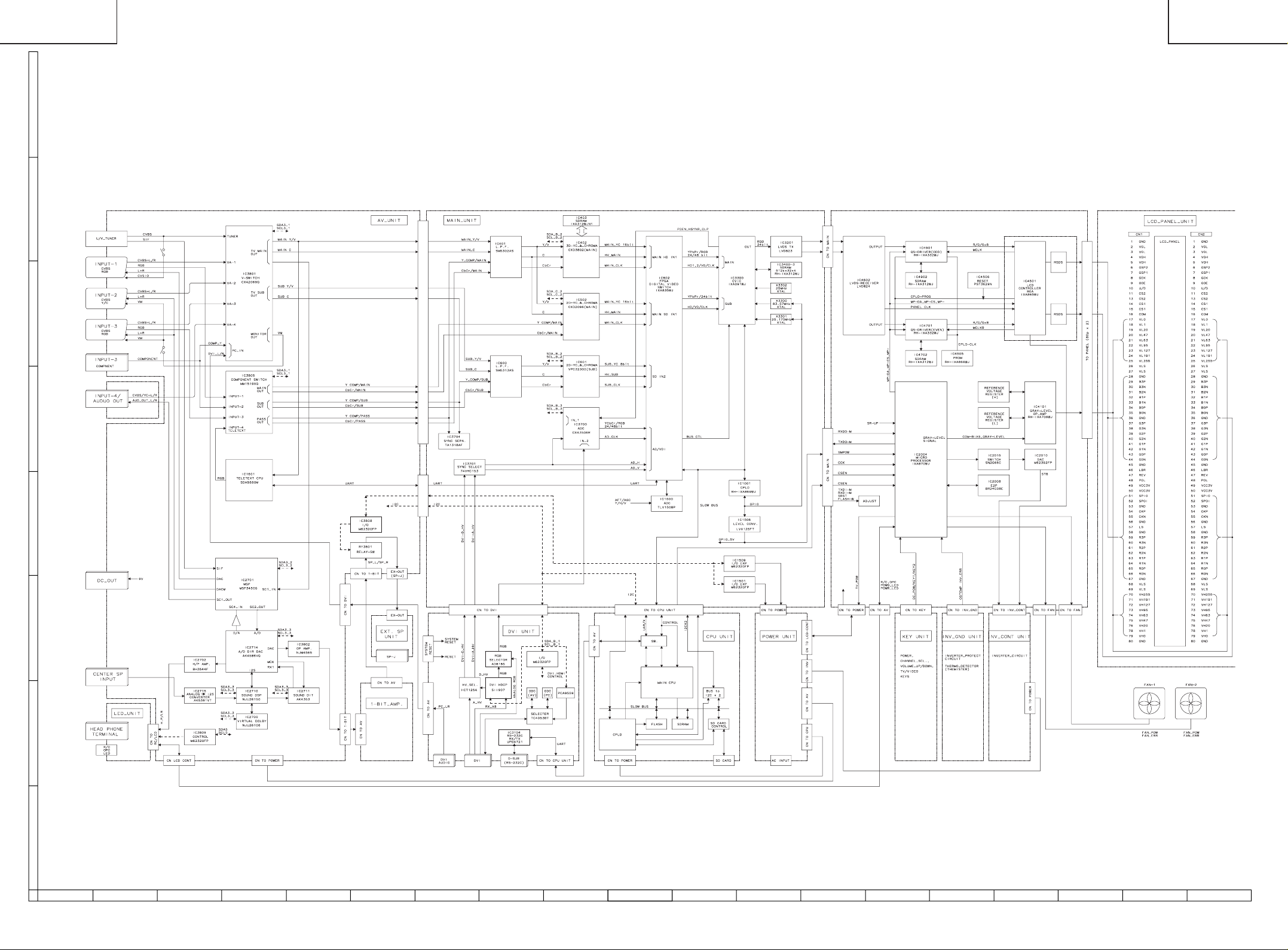
LC-32GA3E
LC-37GA3E
SYSTEM BLOCK DIAGRAM
H
G
F
LC-32GA3E
LC-37GA3E
E
D
C
B
A
48
87109654321
49
1716 19181514131211
Page 2
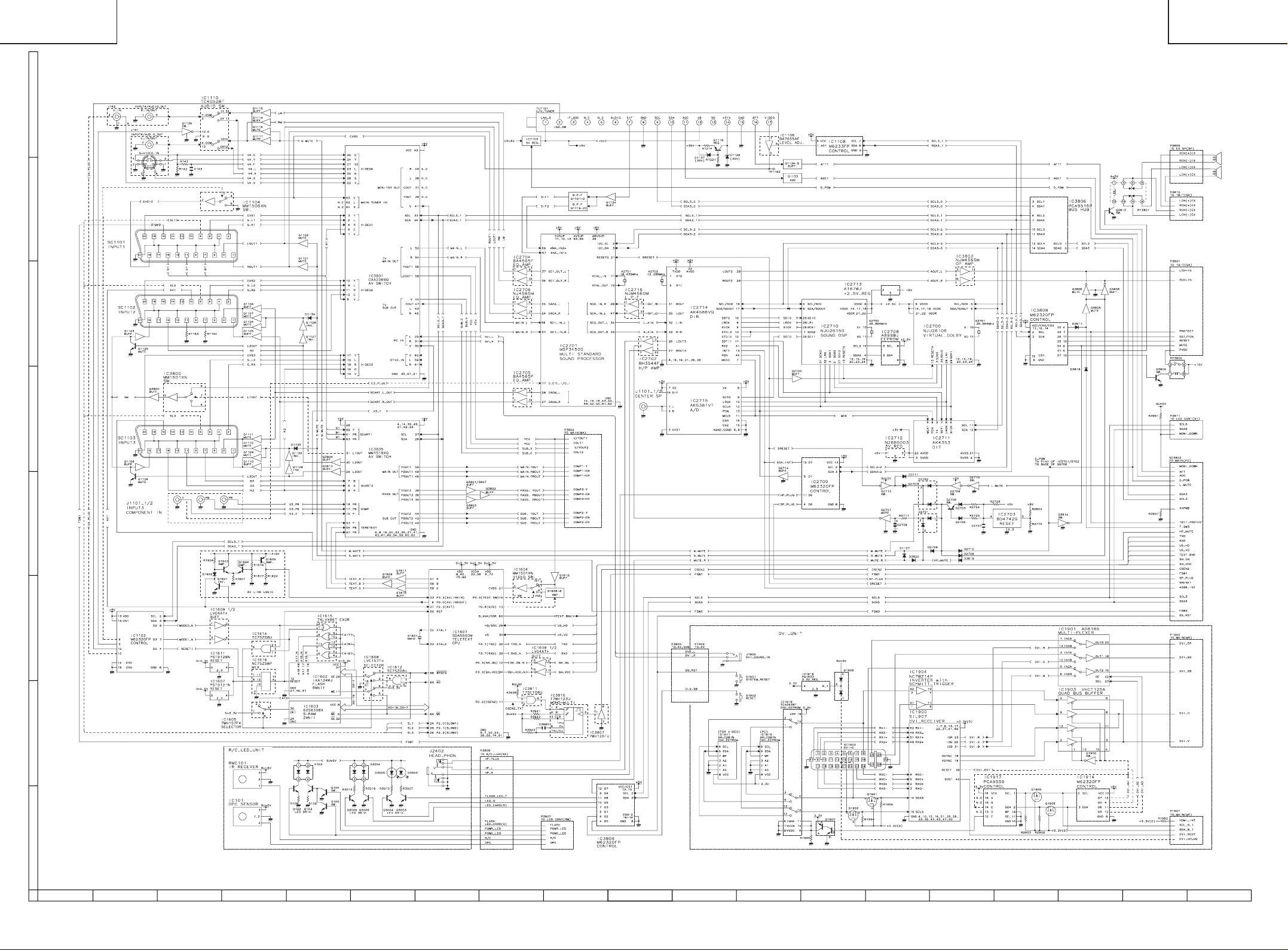
LC-32GA3E
LC-37GA3E
AV BLOCK DIAGRAM
H
G
F
LC-32GA3E
LC-37GA3E
E
D
C
B
A
50
87109654321
51
1716 19181514131211
Page 3
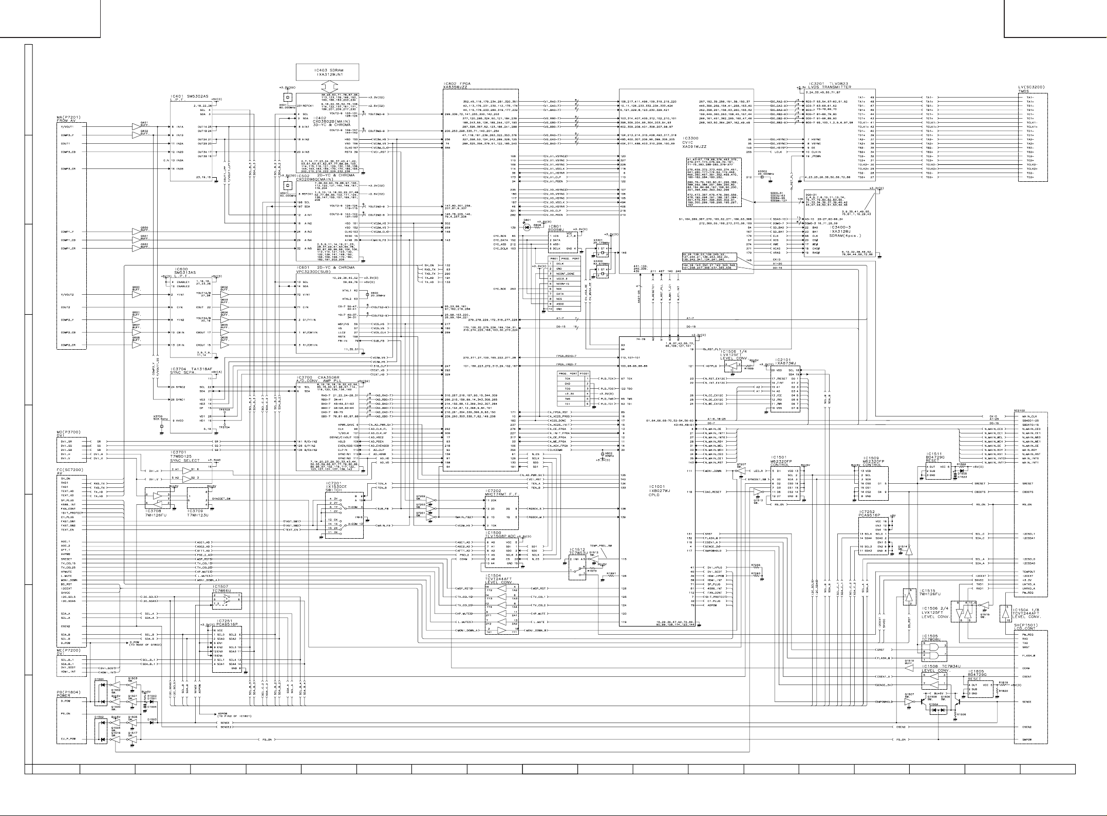
LC-32GA3E
LC-37GA3E
MAIN BLOCK DIAGRAM
H
G
F
LC-32GA3E
LC-37GA3E
E
D
C
B
A
52
87109654321
53
1716 19181514131211
Page 4
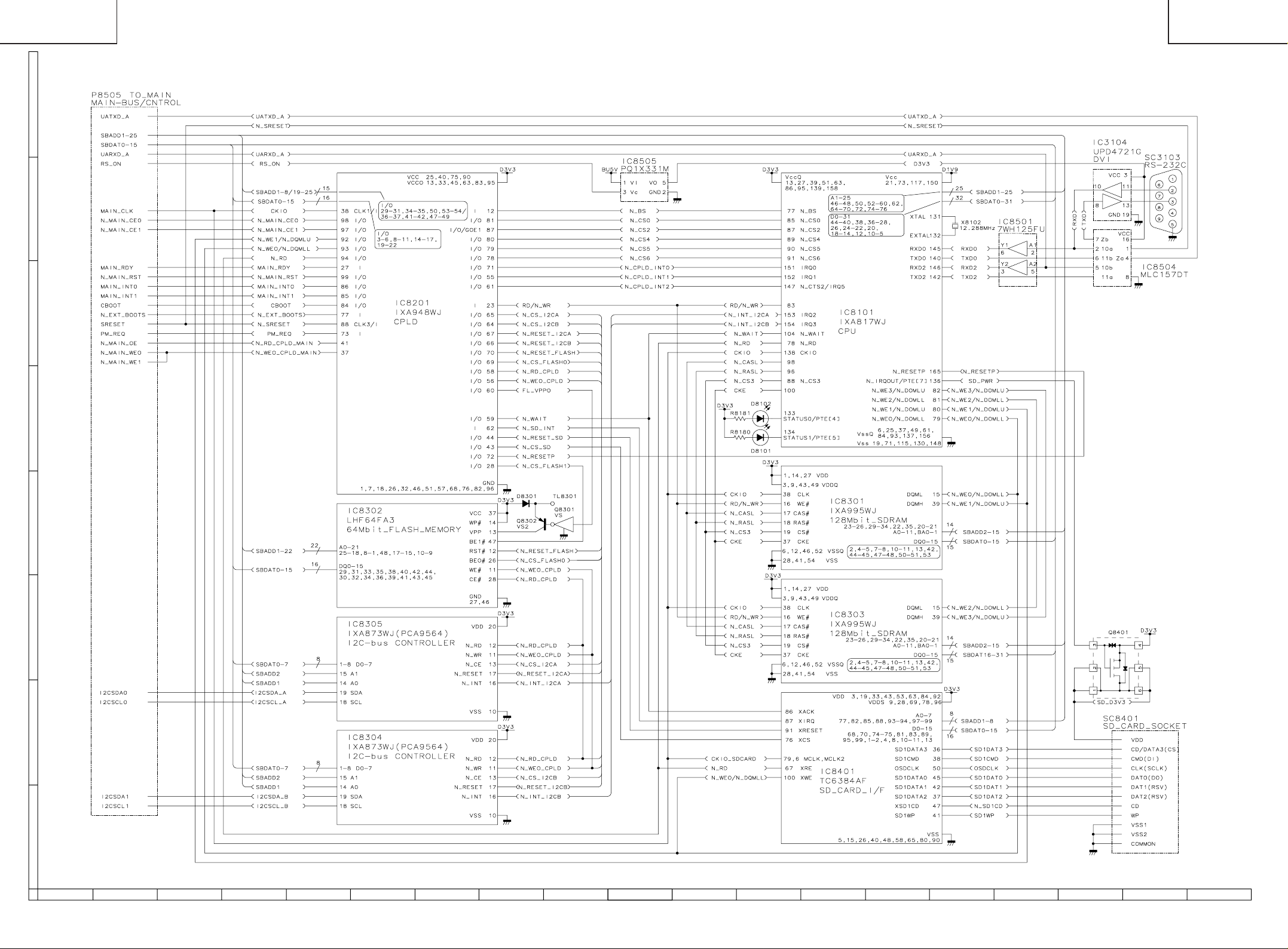
LC-32GA3E
LC-37GA3E
CPU BLOCK DIAGRAM
H
G
F
LC-32GA3E
LC-37GA3E
E
D
C
B
A
54
87109654321
55
1716 19181514131211
Page 5
LC-32GA3E
LC-37GA3E
DISPLAY BLOCK DIAGRAM
H
G
F
LC-32GA3E
LC-37GA3E
E
D
C
B
A
56
87109654321
57
1716 19181514131211
Page 6
LC-32GA3E
LC-37GA3E
POWER BLOCK DIAGRAM
H
G
F
LC-32GA3E
LC-37GA3E
E
D
C
B
A
58
87109654321
59
1716 19181514131211
Page 7
LC-32GA3E
LC-37GA3E
OVERALL WIRING DIAGRAM (LC-32GA3E)
H
G
F
LC-32GA3E
LC-37GA3E
E
D
C
B
A
60
87109654321
61
1716 19181514131211
Page 8
LC-32GA3E
LC-37GA3E
OVERALL WIRING DIAGRAM (LC-37GA3E)
H
G
F
LC-32GA3E
LC-37GA3E
E
D
C
B
A
62
87109654321
63
1716 19181514131211
Page 9
1
1
Ë
CPU Unit-1/5
H
G
F
E
D
C
B
A
87
109654321
11312 1514 1716 1918 2120
D33 D34
Page 10
1
1
Ë
CPU Unit-2/5
H
G
F
E
D
C
B
A
87
109654321
11312 1514 1716 1918 2120
D35 D36
Page 11
1
1
Ë
CPU Unit-3/5
H
G
F
E
D
C
B
A
87
109654321
11312 1514 1716 1918 2120
D37 D38
Page 12
1
1
Ë
CPU Unit-4/5
H
G
F
E
D
C
B
A
87
109654321
11312 1514 1716 1918 2120
D39 D40
Page 13
1
1
Ë
CPU Unit-5/5
H
G
F
E
D
C
B
A
87
109654321
11312 1514 1716 1918 2120
D41 D42
Page 14
1
1
Ë
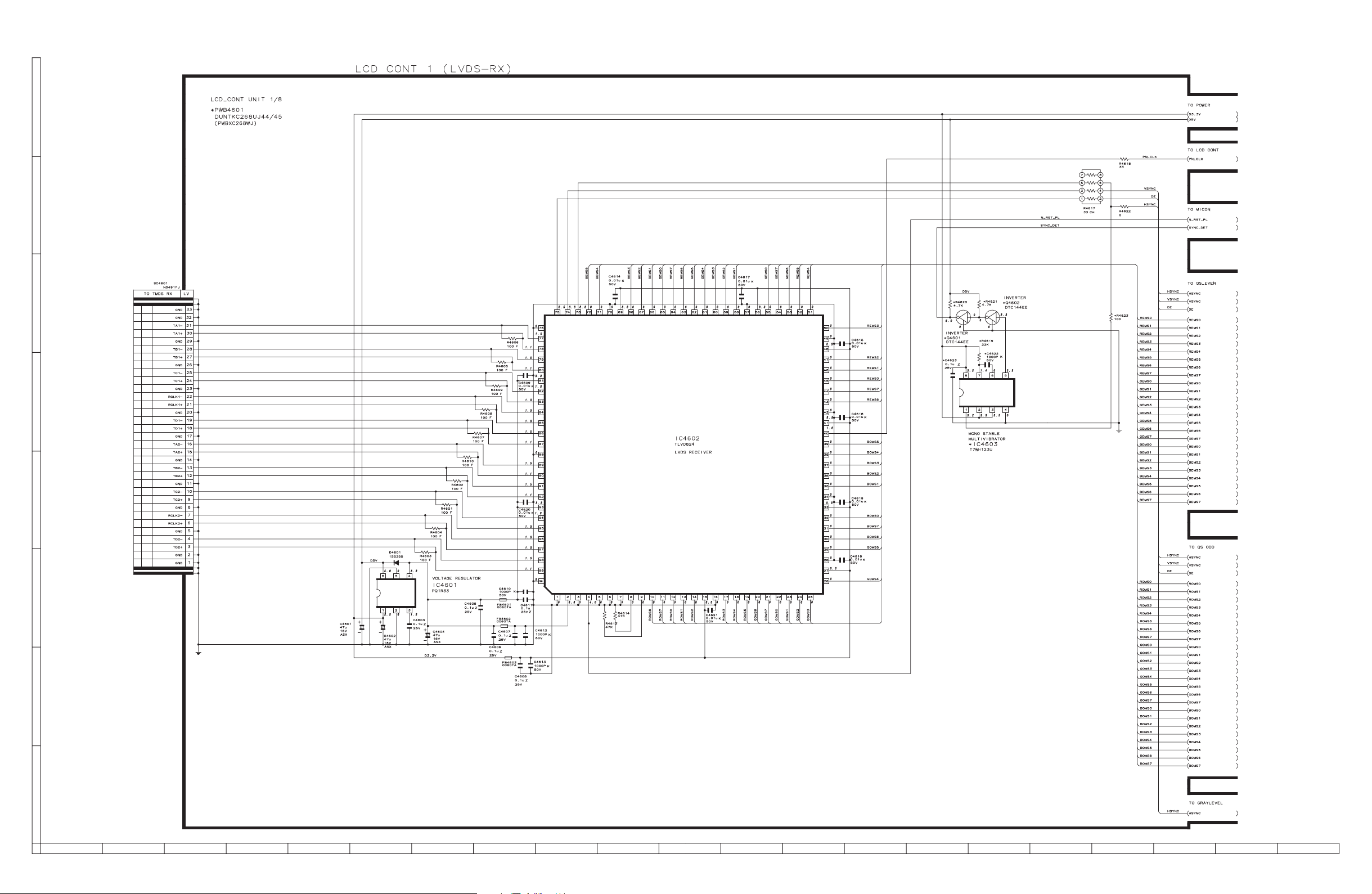
LCD CONTROL Unit-1/8
H
G
F
E
D
C
B
A
87
109654321
11312 1514 1716 1918 2120
D17 D18
Page 15
1
1
Ë
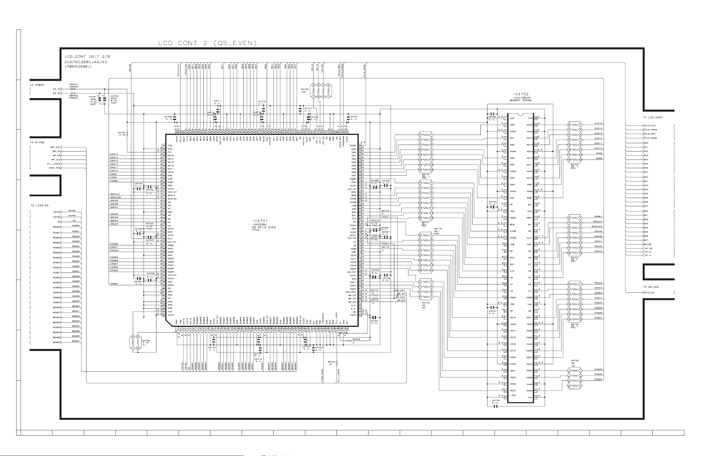
LCD CONTROL Unit-2/8
H
G
F
E
D
C
B
A
87
109654321
11312 1514 1716 1918 2120
D19 D20
Page 16
1
1
Ë
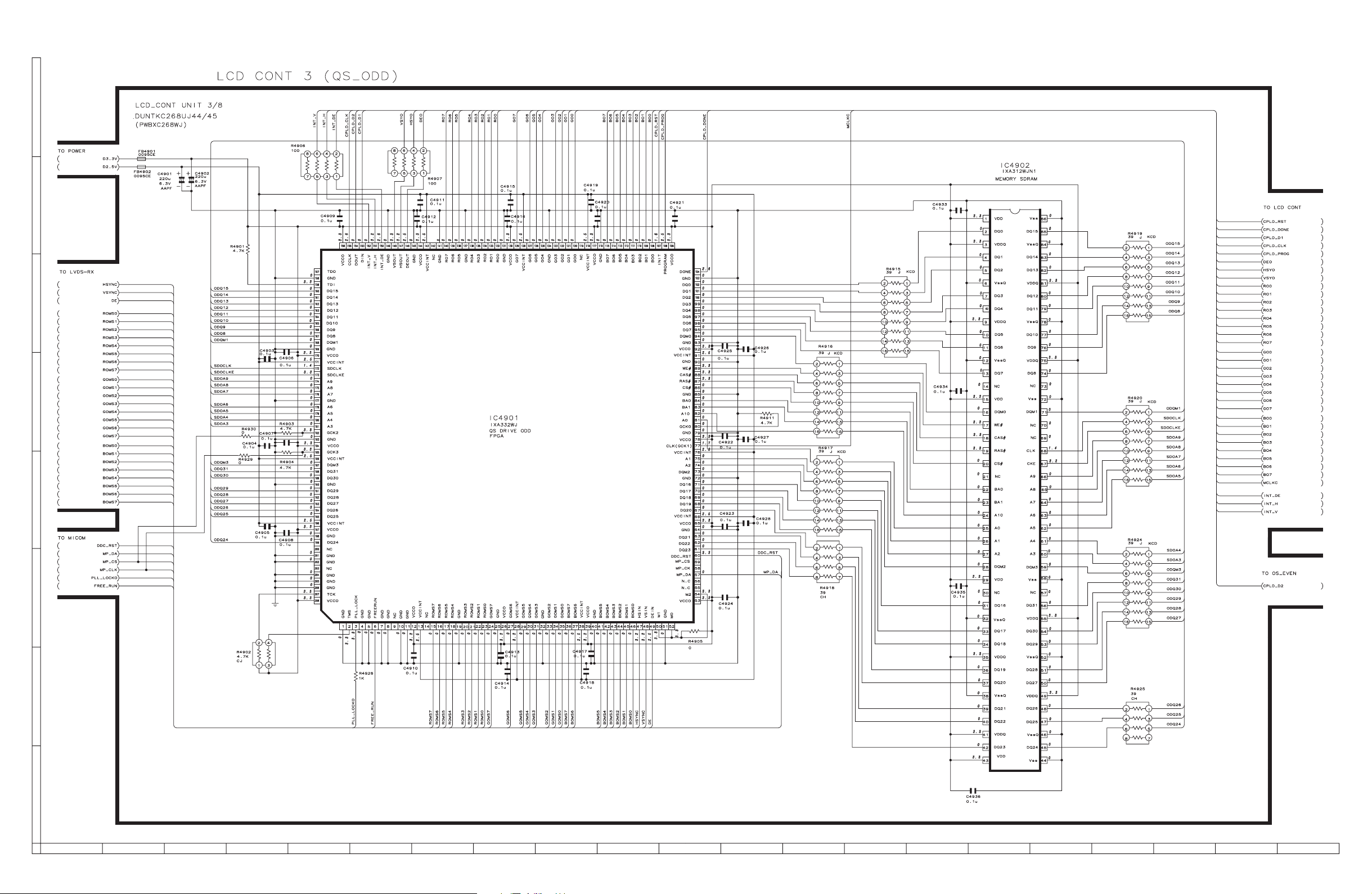
LCD CONTROL Unit-3/8
H
G
F
E
D
C
B
A
87
109654321
11312 1514 1716 1918 2120
D21 D22
Page 17
1
1
Ë
LCD CONTROL Unit-4/8
H
G
F
E
D
C
B
A
87
109654321
11312 1514 1716 1918 2120
D23 D24
Page 18
1
1
Ë
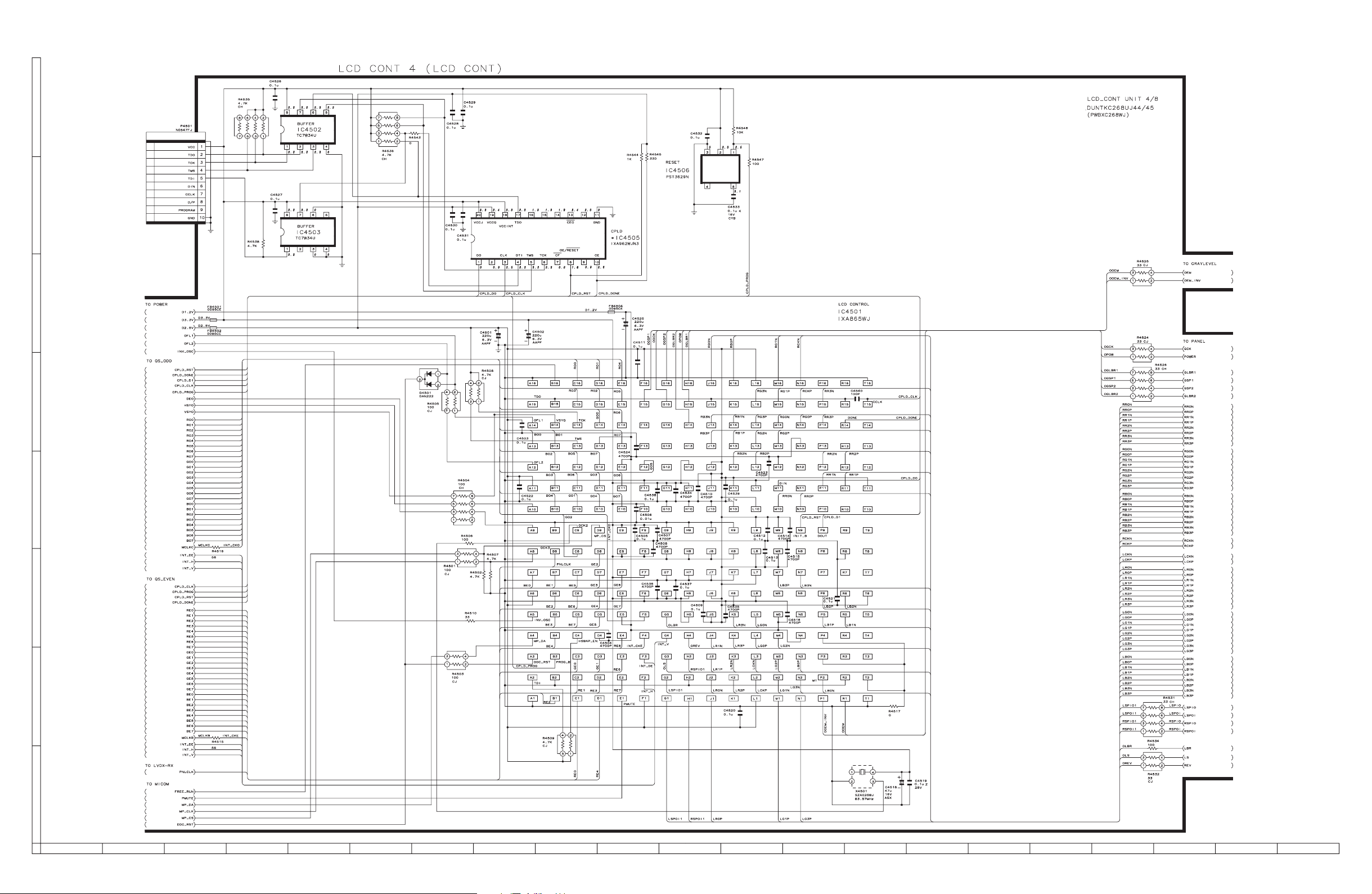
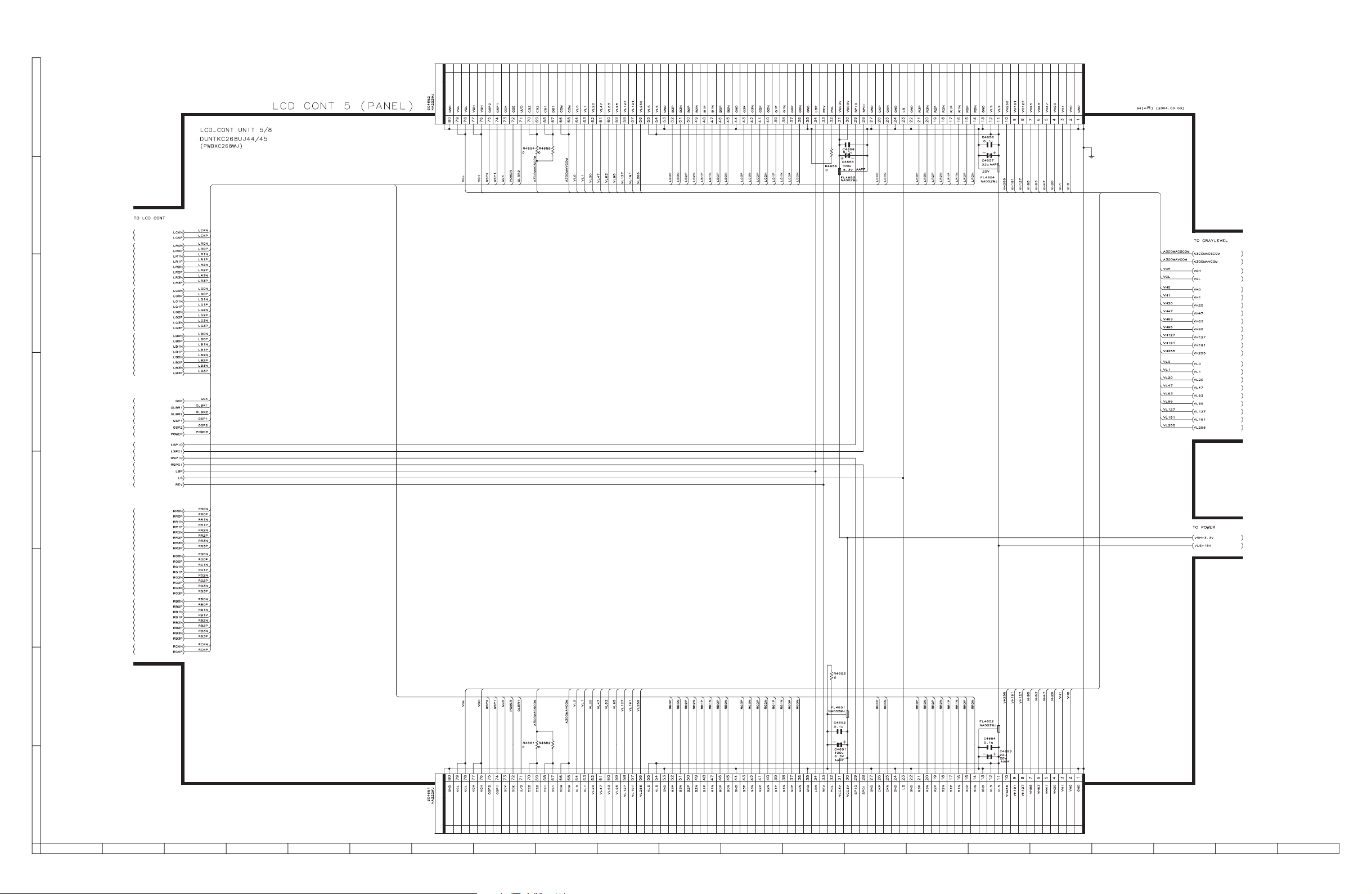
LCD CONTROL Unit-5/8
H
G
F
E
D
C
B
A
87
109654321
11312 1514 1716 1918 2120
D25 D26
Page 19
1
1
Ë
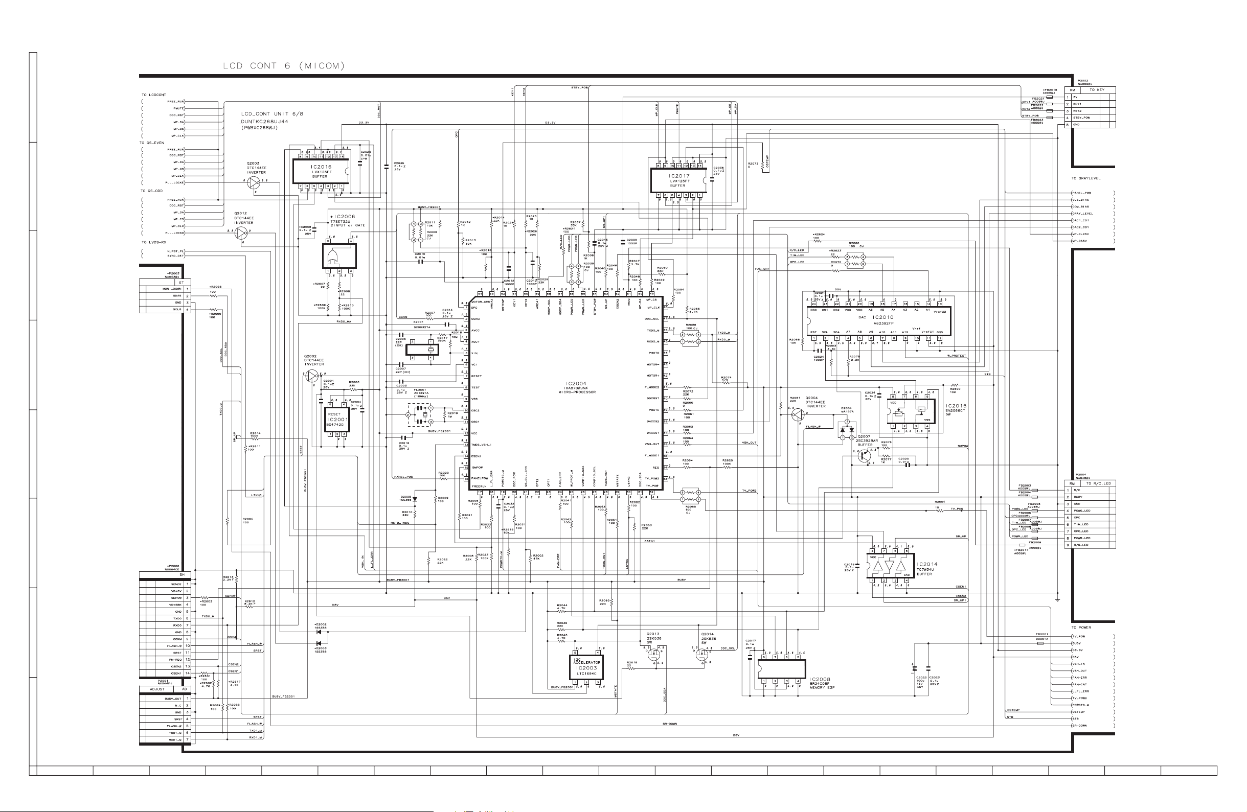
LCD CONTROL Unit-6/8
H
G
F
E
D
C
B
A
87
109654321
11312 1514 1716 1918 2120
D27 D28
Page 20
1
1
Ë
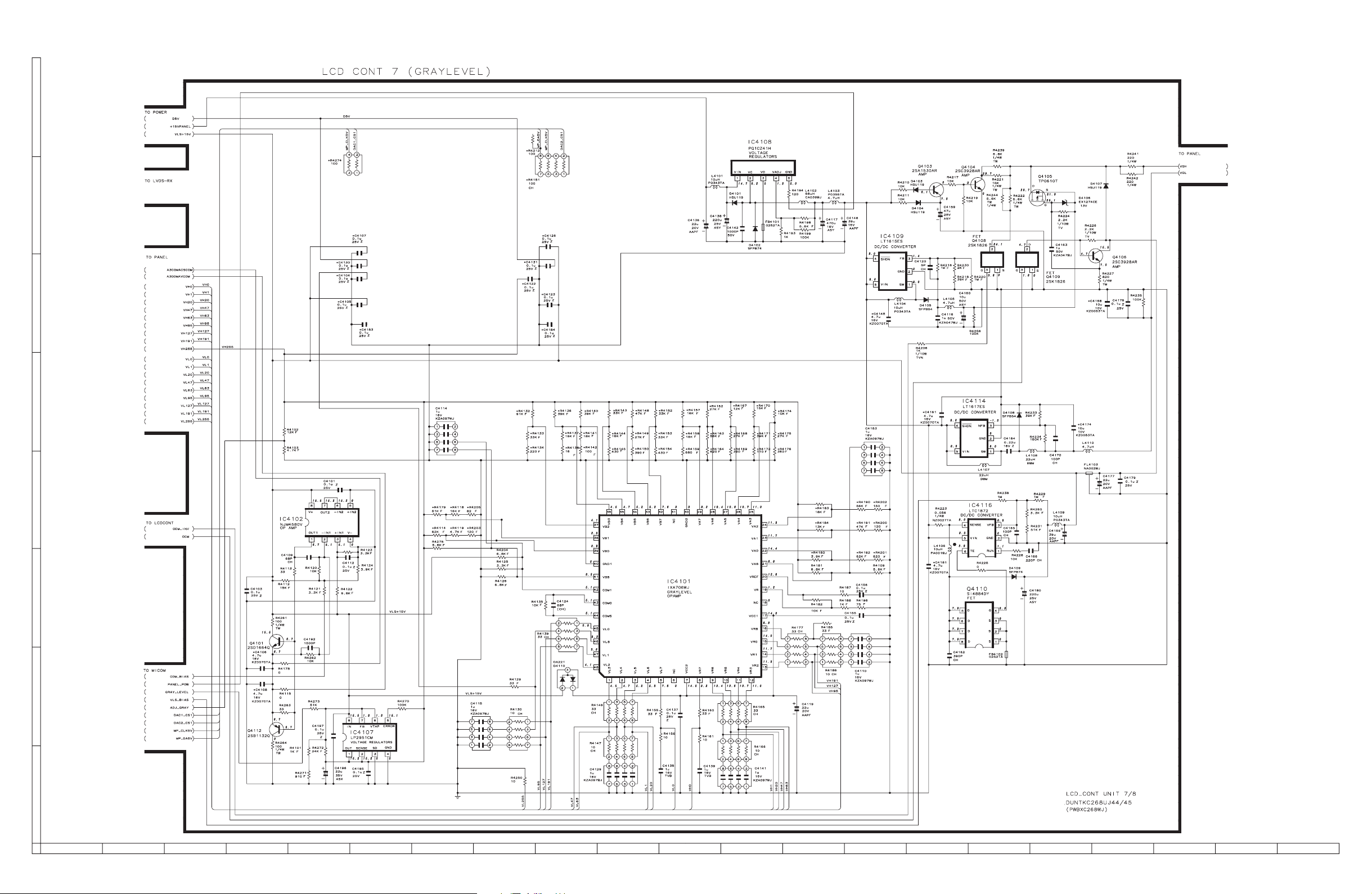
LCD CONTROL Unit-7/8
H
G
F
E
D
C
B
A
87
109654321
11312 1514 1716 1918 2120
D29 D30
Page 21

1
1
Ë
LCD CONTROL Unit-8/8
H
G
F
E
D
C
B
A
87
109654321
11312 1514 1716 1918 2120
D31 D32
Page 22

1
1
Ë
DVI Unit-1/2
H
G
F
E
D
C
B
A
87
109654321
11312 1514 1716 1918 2120
D71 D72
Page 23

1
1
Ë
DVI Unit-2/2
H
G
F
E
D
C
B
A
87
109654321
11312 1514 1716 1918 2120
D73 D74
Page 24

Ë
KEY Unit
Ë
R/C, LED Unit
H
G
F
E
H
G
F
E
D
C
B
A
D
C
B
A
654321
D13 D14
654321
Page 25

Ë
EXT, SP, TERMINAL Unit
H
G
F
E
H
G
F
E
D
C
B
A
D
C
B
A
D89
654321
654321
Page 26

1
1
Ë
AV Unit-1/5
H
G
F
E
D
C
B
A
87
109654321
11312 1514 1716 1918 2120
D4D3
Page 27

1
Ë
AV Unit-2/5
H
G
F
E
D
C
B
A
87
109654321
11312 1514 1716 1918 2120
D5 D6
Page 28

1
Ë
AV Unit-3/5
H
G
F
E
D
C
B
A
87
109654321
11312 1514 1716 1918 2120
D7 D8
Page 29

1
Ë
AV Unit-4/5
H
G
F
E
D
C
B
A
87
109654321
11312 1514 1716 1918 2120
D9 D10
Page 30

1
Ë
AV Unit-5/5
H
G
F
E
D
C
B
A
87
109654321
11312 1514 1716 1918 2120
D11 D12
Page 31

1
Ë
FRONT Unit
H
G
F
E
D
C
B
A
87
109654321
11312 1514 1716 1918 2120
D15 D16
Page 32

1
Ë
MAIN Unit-1/14
H
G
F
E
D
C
B
A
87
109654321
11312 1514 1716 1918 2120
D43 D44
Page 33

1
Ë
MAIN Unit-2/14
H
G
F
E
D
C
B
A
87
109654321
11312 1514 1716 1918 2120
D45 D46
Page 34

1
Ë
MAIN Unit-3/14
H
G
F
E
D
C
B
A
87
109654321
11312 1514 1716 1918 2120
D47 D48
Page 35

1
Ë
MAIN Unit-4/14
H
G
F
E
D
C
B
A
87
109654321
11312 1514 1716 1918 2120
D49 D50
Page 36

1
Ë
MAIN Unit-5/14
H
G
F
E
D
C
B
A
87
109654321
11312 1514 1716 1918 2120
D51 D52
Page 37

1
Ë
MAIN Unit-6/14
H
G
F
E
D
C
B
A
87
109654321
11312 1514 1716 1918 2120
D53 D54
Page 38

1
Ë
MAIN Unit-7/14
H
G
F
E
D
C
B
A
87
109654321
11312 1514 1716 1918 2120
D55 D56
Page 39

1
Ë
MAIN Unit-8/14
H
G
F
E
D
C
B
A
87
109654321
11312 1514 1716 1918 2120
D57 D58
Page 40

1
Ë
MAIN Unit-9/14
H
G
F
E
D
C
B
A
87
109654321
11312 1514 1716 1918 2120
D59 D60
Page 41

1
Ë
MAIN Unit-10/14
H
G
F
E
D
C
B
A
87
109654321
11312 1514 1716 1918 2120
D61 D62
Page 42

1
Ë
MAIN Unit-11/14
H
G
F
E
D
C
B
A
87
109654321
11312 1514 1716 1918 2120
D63 D64
Page 43

1
Ë
MAIN Unit-12/14
H
G
F
E
D
C
B
A
87
109654321
11312 1514 1716 1918 2120
D65 D66
Page 44

1
Ë
MAIN Unit-13/14
H
G
F
E
D
C
B
A
87
109654321
11312 1514 1716 1918 2120
D67 D68
Page 45

1
Ë
MAIN Unit-14/14
H
G
F
E
D
C
B
A
87
109654321
11312 1514 1716 1918 2120
D69 D70
Page 46

1
Ë
INVERTER-A Unit (LC-37GA3E)
H
G
F
E
D
C
B
A
P7505
B3PS-VH
LUG7502
SD01138-21
LUG7501
SD01138-21
B12B-PASK-1
12PL-FJ
1
2
3
P7506
1
2
3
4
5
6
7
8
9
10
11
12
P7507
1
2
3
4
5
6
7
8
9
10
11
12
Vin
N.C
GND
R7546
N.M
R7547
N.M
S GND
STB
OFL1
OFL2
INV OSC
INV ERR
REG1
IS1-1
IS1-2
REG2
IS2-1
IS2-2
GND
+B5-12V
S GND
STB
OFL2
INV OSC
INV ERR
SRT
SS
REG2
IS2-1
IS2-2
SD01138-21
LUG7503
R7569
N.M
C7566
0.01uF 50V
R7543
0
R7545
0
R7570
N.M
H-0017-2
LUG7504
SD01138-21
R7549
0 (3225)
R7544
N.M
FH7502
R7533
1K F
U.CODE RUNTKA080WJZZ
F7501
FH7501
1SS355
D7523
5
6
C7552
N.M
C7551
N.M
1
2
H-0017-2
R7555
51k F
R7513
47K F
Q7511
UM6K1N
R7532
N.M
R7531
N.M
R7537
1.1K F
R7525
0
R7536
1.1K F
TLC 10A 250V
R7548
0 (3225)
R7539
51kF
3
4
R7522
N.M
R7521
75KF
C7567
N.M
R7517
R7524
N.M
C7545
N.M
100K F
100K F
R7530
R7538
N.M
100 F
R7556
75KF
R7523
R7541
N.M
R7512
36k
F
C7548
N.M
R7509
R7510
R7511
C7544
330p CH
4700pF/50V
C7547
2200pF
4700pF/50V
C7550
2200pF
R7540
0
R7516
0
68K F
68K F
1K F
C7546
C7549
IC7502
BA00ASFP
R7529
100
R7520
N.M
BD9766FV
IC7501
DUTY
BRT
BCT
RDIS
RT
SRT
CT
GND
FB1
IS1
VS1
FB2
IS2
VS2
4
5
3
VCC
P1
N1
PGND
N2
P2
SCP2
SCP1
SS
REG
COMP2
COMP1
STB
FAIL
D7521
R7507
10K F
HZU5.1B
C7534
C7535
C7537
C7555
C7538
C7533
0.047uF 16V
330uF 25V KZE
330uF 25V KZE
D7522
HZU5.1B
C7536
0.047uF 16V
330uF 25V KZE
330uF 25V
KZE
330uF 25V
KZE
R7515
C7540
C7541
C7542
C7543
R7527
R7528
100 F
100
6.8K F
R7514
2.2K F
C7539
4.7u 25V
(3216)
2.2u 10V
2.2u 10V
0.22u 16V
0.1u 16V
10K F
10K F
R7518
R7519
(2125)
(2125)
0
0
R7535
N.M
R7557
12
0
(1608)
R7558
N.M
R7534
R7526
R7560
(3216)
R7508
10K F
R7564
(3216)
RSS075P03
R7559
0
(3216)
0
RSS100N03
RSS075P03
R7561
0
(3216)
R7562
0
(3216)
RSS100N03
R7563
0
(3216)
0
RSS100N03
RSS075P03
R7565
0
(3216)
R7566
0
(3216)
RSS100N03
RSS075P03
R7567
0
(3216)
R7568
0
(3216)
RSS100N03
1,2,3
Q7501
4
5,6,7,8
5,6,7,8
Q7506
4
1,2,3
1,2,3
Q7502
4
5,6,7,8
5,6,7,8
Q7507
4
1,2,3
RSS075P03
1,2,3
Q7503
4
5,6,7,8
5,6,7,8
Q7508
4
1,2,3
RB070M30
1,2,3
Q7504
4
5,6,7,8
5,6,7,8
Q7509
4
1,2,3
1,2,3
Q7505
4
5,6,7,8
5,6,7,8
Q7510
4
1,2,3
RB070M30
RB070M30
D7511
D7512
RB070M30
RB070M30
D7513
D7514
RB070M30
RB070M30
D7515
D7516
RB070M30
D7517
D7518
RB070M30
RB070M30
D7519
D7520
4.7u 25V
(3216)
C7523
C7524
4.7u 25V
(3216)
4.7u 25V
(3216)
C7525
C7526
4.7u 25V
(3216)
4.7u 25V
(3216)
C7527
C7528
4.7u 25V
(3216)
4.7u 25V
(3216)
C7529
C7530
4.7u 25V
(3216)
4.7u 25V
(3216)
C7531
C7532
4.7u 25V
(3216)
5,6,7,8
1,2,3,4
BLCP4220
5,6,7,8
1,2,3,4
BLCP4220
5,6,7,8
1,2,3,4
BLCP4220
5,6,7,8
1,2,3,4
BLCP4220
5,6,7,8
1,2,3,4
BLCP4220
T7501
T7502
T7503
T7504
T7505
C7503
C7504
C7505
C7508
C7509
C7512
C7513
C7516
C7517
C7520
C7521
0.022uF 25V
12pF 5kV
(ECC)
12pF 5kV
(ECC)
C7506
0.022uF 25V
C7507
0.022uF 25V
12pF 5kV
(ECC)
12pF 5kV
(ECC)
C7510
0.022uF 25V
C7511
0.022uF 25V
12pF 5kV
(ECC)
12pF 5kV
(ECC)
C7514
0.022uF 25V
C7515
0.022uF 25V
12pF 5kV
(ECC)
12pF 5kV
(ECC)
C7518
0.022uF 25V
C7519
0.022uF 25V
12pF 5kV
(ECC)
12pF 5kV
(ECC)
C7522
0.022uF 25V
9
12
13
16
9
12
13
16
9
12
13
16
9
12
13
16
9
12
13
16
R7505
0
R7506
0
C7502
D7501
DAN217U
D7502
DAN217U
D7503
DAN217U
D7504
DAN217U
C7501
N.M
D7505
DAN217U
D7506
DAN217U
D7507
DAN217U
D7508
DAN217U
D7509
DAN217U
D7510
DAN217U
N.M
R7501
33K F
R7502
68K F
R7503
33K F
R7504
68K F
P7501
1
3
1717823-1
P7502
1
3
1717823-1
P7503
1
3
1717823-1
P7504
1
3
1717823-1
P7508
1
3
1717823-1
87
109654321
11312 1514 1716 1918 2120
D83 D84
Page 47

1
Ë
INVERTER-B Unit (LC-37GA3E)
U.CODE RUNTKA081WJZZ
FH7401
H-0017-2
R7429
1K F
F7401
TLC 10A 250V
1SS355
D7415
FH7402
H-0017-2
(3225)
R7445
0
4
5
IC7403
3
12
N.M
R7446
N.M
R7447
N.M
R7448
N.M
R7449
N.M
C7423
C7408
B2PS-VH
LUG7402
SD01138-21
LUG7401
SD01138-21
LUG7403
SD01138-21
P7404
1
2
Vin
GND
R7424
N.M
R7437
N.M
R7458
N.M
H
G
F
D7414
HZU5.1B
C7422
0.047uF 16V
330uF 25V KZE
330uF 25V KZE
R7409
10K F
R7450
0
(3216)
R7451
0
(3216)
RSS100N03
R7452
0
(3216)
R7453
0
(3216)
RSS100N03
RSS075P03
1,2,3
Q7407
4
5,6,7,8
5,6,7,8
Q7409
4
1,2,3
RSS075P03
1,2,3
Q7401
4
5,6,7,8
5,6,7,8
Q7403
4
1,2,3
RB070M30
D7412
D7413
RB070M30
RB070M30
D7403
D7404
RB070M30
4.7u 25V
(3216)
C7420
C7421
4.7u 25V
(3216)
4.7u 25V
(3216)
C7405
C7406
4.7u 25V
(3216)
5,6,7,8
1,2,3,4
BLCP4220
5,6,7,8
1,2,3,4
BLCP4220
T7403
T7401
C7416
C7417
C7418
C7402
C7403
0.022uF 25V
12pF 5kV
(ECC)
12pF 5kV
(ECC)
C7419
0.022uF 25V
C7401
0.022uF 25V
12pF 5kV
(ECC)
12pF 5kV
(ECC)
C7404
0.022uF 25V
9
12
13
16
9
12
13
16
R7403
0
D7410
DAN217U
D7411
DAN217U
D7401
DAN217U
D7402
DAN217U
C7407
N.M
R7401
33K F
R7402
68K F
P7401
1
3
1717823-1
P7402
1
3
1717823-1
E
R7430
R7438
0
100
R7412
C7425
100 F
N.M
R7414
N.M
D
R7442
51k F
R7441
P7405
GND
1
+B5-12V
C
B
A
2
3
4
5
6
7
8
9
10
11
12
12R-FJ
S GND
STB
OFL2
INV OSC
INV ERR
SRT
SS
REG2
IS2-1
IS2-2
R7444
0
(3225)
R7439
N.M
51kF
3
4
R7433
5
6
C7446
N.M
C7445
N.M
N.M
1
2
R7440
47K F
Q7402
UM6K1N
R7417
N.M
R7410
N.M
R7422
1.1K F
R7411
1.1K F
R7420
N.M
R7418
75K F
C7455
N.M
R7443
75KF
C7437
N.M
100K F
R7407
100K F
R7408
R7419
36k
F
R7416
R7428
R7421
C7438
330p CH
4700pF/50V
C7427
2200pF
4700pF/50V
C7429
2200pF
C7426
C7428
R7415
0
68K F
68K F
1K F
IC7402
DUTY
BRT
BCT
RDIS
RT
SRT
CT
GND
FB1
IS1
VS1
FB2
IS2
VS2
R7413
N.M
BD9766FV
VCC
PGND
SCP2
SCP1
REG
COMP2
COMP1
STB
FAIL
R7432
0
D7417
HZU5.1B
C7415
C7444
C7431
0.047uF 16V
330uF 25V KZE
330uF 25V
KZE
C7432
4.7u 25V
C7433
C7434
C7435
C7436
R7426
R7427
100
100
(3216)
2.2u 10V
(2125)
2.2u 10V
(2125)
0.22u 16V
0.1u 16V
10K F
10K F
P1
N1
N2
P2
SS
R7435
R7431
R7436
10K F
R7454
0
(3216)
R7455
0
(3216)
RSS100N03
R7456
0
(3216)
R7457
0
(3216)
RSS100N03
RSS075P03
1,2,3
Q7404
4
5,6,7,8
5,6,7,8
Q7406
4
1,2,3
RSS075P03
1,2,3
Q7410
4
5,6,7,8
5,6,7,8
Q7411
4
1,2,3
RB070M30
D7408
D7409
RB070M30
RB070M30
D7420
D7421
RB070M30
4.7u 25V
(3216)
C7413
C7414
4.7u 25V
(3216)
4.7u 25V
(3216)
C7424
C7430
4.7u 25V
(3216)
5,6,7,8
1,2,3,4
BLCP4220
5,6,7,8
1,2,3,4
BLCP4220
T7402
T7404
C7409
C7410
C7411
C7440
C7441
0.022uF 25V
12pF 5kV
(ECC)
12pF 5kV
(ECC)
C7412
0.022uF 25V
C7439
0.022uF 25V
12pF 5kV
(ECC)
12pF 5kV
(ECC)
C7442
0.022uF 25V
9
12
13
16
9
12
13
16
R7406
0
C7443
N.M
D7406
DAN217U
D7407
DAN217U
D7418
DAN217U
D7419
DAN217U
R7404
33K F
R7405
68K F
P7403
1
3
1717823-1
P7406
1
3
1717823-1
87
109654321
11312 1514 1716 1918 2120
D85 D86
Page 48

Ë
INVERTER GROUND-A Unit (LC-37GA3E)
Ë
INVERTER GROUND-B Unit (LC-37GA3E)
H
RUNTKA082WJZZ
G
F
E
D
C
B
A
1717823-1
MP
1717823-1
1717823-1
1717823-1
1717823-1
P7601
1
3
P7602
1
3
P7603
1
3
P7604
1
3
P7605
1
3
TH7601
N.M
TH7602
N.M
TH7603
N.M
TH7604
N.M
R7605
IK
R7618
IK
R7606
IK
R7621
IK
R7629
1.3KF
R7609
IK
R7623
IK
R7615
IK
R7625
R7630
0
DAN217U
IK
R7627
1.3KF
R7628
0
DAN217U
DAN217U
DAN217U
DAN217U
D7606
DAN217U
D7608
DAN217U
D7601
D7603
DAN217U
D7605
D7607
DAN217U
D7602
D7604
R7616
D7609
DAN217U
D7610
R7611
1M
1M
R7602
1M
R7608
1M
R7613
1M
R7619
1M
R7604
1M
R7622
1M
R7626
N.M
R7624
N.M
1u 25V
(3216)
1u 25V
(3216)
(3216)
UM6K1N
C7604
UM6K1N
C7606
C7608
N.M
UM6K1N
C7601
1u 25V
(3216)
UM6K1N
C7603
1u 25V
(3216)
UM6K1N
C7605
1u 25V
UM6K1N
C7607
1u 25V
(3216)
UM6K1N
C7602
1u 25V
(3216)
R7610
100K F
R7614
100K F
UM6K1N
C7609
1u 25V
(3216)
C7610
N.M
R7601
100K F
R7607
100K F
R7612
100K F
R7617
100K F
R7603
100K F
6
2
1
6
2
1
R7620
100K F
2
2
2
2
2
Q7604
Q7606
2
6
Q7601
1
6
Q7603
1
6
Q7605
1
6
Q7607
1
6
Q7602
1
5
5
6
Q7608
1
H
P7608
OSTEMP
1
SGND
2
REG1
3
IS1-1
3
5
4
3
5
4
3
5
4
3
5
4
3
5
4
3
4
3
4
3
5
4
R7634
0
(3225)
R7633
0
(3225)
R7632
0
(3225)
R7631
0
(3225)
IS1-2
REG2
IS2-1
IS2-2
OSTEMP
SGND
REG1
IS1-1
IS1-2
REG2
IS2-1
IS2-2
S8B-PASK-2
OSTEMP
SGND
REG2
IS2-1
IS2-2
N.C
N.M
P7606
P7607
06PL-FJ
4
5
6
7
8
1
2
3
4
5
6
7
8
1
2
3
4
5
6
LUG7604
SD01138-21
LUG7603
SD01138-21
LUG7602
SD01138-21
LUG7601
SD01138-21
RUNTKA083WJZZ
PSD-0376-D
G
MP
F
E
D
C
B
A
P7651
1
3
1717823-1
P7652
1
3
1717823-1
P7653
1
3
1717823-1
P7654
1
3
1717823-1
R7667
IK
TH7651
NCP18XH103J03RB
R7661
IK
R7654
IK
TH7652
N.M
R7663
IK
R7656
IK
TH7653
N.M
R7668
IK
R7673
1.3KF
R7674
TH7654
N.M
0
R7670
1.3KF
R7671
0
DAN217U
DAN217U
DAN217U
DAN217U
D7657
DAN217U
D7655
D7653
DAN217U
D7651
D7654
DAN217U
D7652
D7656
DAN217U
D7658
R7666
1M
R7658
R7653
1M
R7660
R7655
1M
R7664
R7672
N.M
R7669
C7657
N.M
N.M
R7665
100K F
UM6K1N
C7655
1u 25V
(3216)
R7657
100K F
UM6K1N
1M
1M
1M
C7653
1u 25V
(3216)
C7651
1u 25V
(3216)
C7654
1u 25V
(3216)
C7652
1u 25V
(3216)
C7656
1u 25V
(3216)
C7658
N.M
R7652
100K F
UM6K1N
R7659
100K F
UM6K1N
R7651
100K F
UM6K1N
R7662
100K F
UM6K1N
3
5
6
4
2
Q7655
1
P7655
OSTEMP
1
3
5
6
4
2
Q7653
1
3
5
6
4
2
Q7651
1
3
5
6
4
2
Q7654
1
3
5
6
4
2
Q7652
1
3
5
6
4
2
Q7656
1
R7678
0
R7677
0
R7676
0
R7675
0
(3225)
(3225)
(3225)
SGND
REG2
IS2-1
IS2-2
N.C
2
3
4
5
6
06R-FJ
LUG7654
SD01138-21
LUG7653
SD01138-21
LUG7652
SD01138-21
LUG7651
SD01138-21
654321
D87 D88
654321
Page 49

1
Ë
INVERTER-A Unit (LC-32GA3E)
H
CN7501
Vin
1
N.C
2
GND
3
G
CN7502
S GND
1
F
E
D
2
3
4
5
6
7
8
9
10
11
12
STB
OFL
N.C
INV OSC
INV ERR
REG
IS1
IS2
N.C
N.C
N.C
C7553
R7510
C
B
A
6
123
D7501
R7538
R7542
R7539
R7541
5
4
F7501
R7540
Q7513
U.CODE RUNTKA069WJZZ
JP7502
R7543
R7501
R7502
C7554
R7511
R7512
R7516
R7513
R7514
R7515
C7512
R7508
3
C7501
R7504
R7505
R7506
R7507
R7545
C7502
C7503
C7505
D7518
IC7502
2
R7509
R7503
C7504
C7506
1
IC7501
DUTY
BRT
BCT
RDIS
RT
SRT
CT
GND
FB1
IS1
VS1
FB2
IS2
VS2
C7513
VCC
P1
N1
PGND
N2
P2
SCP2
SCP1
SS
REG
COMP2
COMP1
STB
FAIL
R7524
R7523
R7517
R7525
R7522 R7521
C7511
(3216)
C7510
C7509
C7508
C7507
R7520
R7519
R7518
(2125)
(2125)
12 345
VS2 VCC GND
N2
C7514
P2
R7526
(3216)
C7515
R7527
CN7503
Q7509
Q7510
R7528
(3216)
Q7511
Q7512
C7516
C7517
C7518
C7519
C7520
R7544
R7533
ZD7502
ZD7501
R7529
(3216)
C7555
(3216)
R7530
R7531
(3216)
C7556
(3216)
R7532
R7534
(3216)
C7557
(3216)
R7535
R7536
(3216)
C7558
R7537
(3216)
6
4,5
T7501
D7510
D7511
D7512
D7513
D7514
D7515
D7516
D7517
(3216)
C7521
C7522
(3216)
(3216)
C7523
C7524
(3216)
(3216)
C7525
C7526
(3216)
(3216)
C7527
C7528
(3216)
1,2
4,5
1,2
4,5
1,2
4,5
1,2
4,5
1,2
4,5
1,2
4,5
1,2
1,2
4,5
T7502
T7503
T7504
T7505
T7506
T7507
T7508
C7531
10
10
C7534
6
(3216)
6
C7537
10
10
C7540
6
(3216)
6
C7543
10
10
C7546
6
(3216)
6
C7549
10
10
C7552
6
(3216)
1,2,3
Q7501
4
5,6,7,8
5,6,7,8
Q7502
4
1,2,3
R7547
LUG7502
1,2,3
Q7503
4
5,6,7,8
5,6,7,8
Q7504
4
1,2,3
1,2,3
Q7505
4
5,6,7,8
5,6,7,8
Q7506
4
1,2,3
1,2,3
Q7507
4
5,6,7,8
5,6,7,8
Q7508
4
1,2,3
R7546
LUG7501
(3216)
(3216)
(3216)
(3216)
C7529
C7530
C7532
C7533
C7535
C7536
C7538
C7539
C7541
C7542
C7544
C7545
C7547
C7548
C7550
C7551
D7502
D7503
D7504
D7505
D7506
D7507
D7508
D7509
CN7504
2
1
CN7505
2
1
CN7506
2
1
CN7507
2
1
87
109654321
11312 1514 1716 1918 2120
D77 D78
Page 50

1
Ë
INVERTER-B Unit (LC-32GA3E)
H
U.CODE RUNTKA070WJZZ
VS2 VCC GND N2
CN7402
12 3
P2
45
R7407
ZD7401
R7409
R7408
(3216)
C7440
(3216)
R7410
(3216)
C7441
R7411
(3216)
T7401
4,5
6
1,2
T7402
T7403
T7404
(3216)
10
10
6
6
(3216)
10
10
6
(3216)
C7418
C7421
(3216)
C7424
C7427
1,2,3
Q7401
4
5,6,7,8
5,6,7,8
4
Q7402
1,2,3
R7420
LUG7404
1,2,3
Q7403
4
5,6,7,8
5,6,7,8
Q7404
4
1,2,3
R7417
LUG7401
D7409
D7410
(3216)
D7411
D7412
(3216)
C7408
1,2
(3216)
4,5
1,2
C7409
(3216)
4,5
C7410
1,2
(3216)
4,5
C7411
(3216)
C7416
C7417
C7419
C7420
C7422
C7423
C7425
C7426
D7401
D7402
D7403
D7404
CN7401
2
Vin
GND
F7401
JP7401
G
C7404
R7401
R7402
F
C7401
R7403
R7404
E
(3216)
Q7409
Q7410
C7403
C7405
CN7403
21
1
CN7404
2
1
D
C7402
R7405
C
R7406
(3216)
Q7411
Q7412
C7406
B
C7407
A
R7416
ZD7402
R7412
(3216)
C7442
R7413
(3216)
R7414
(3216)
C7443
R7415
(3216)
T7405
4,5
6
C7428
C7429
C7431
C7432
C7434
C7435
C7437
C7438
D7405
D7406
D7407
D7408
10
10
6
(3216)
6
10
10
6
(3216)
(3216)
C7430
C7433
(3216)
C7436
C7439
1,2,3
Q7405
4
5,6,7,8
5,6,7,8
Q7406
4
1,2,3
R7418
LUG7402
1,2,3
Q7407
4
5,6,7,8
5,6,7,8
Q7408
4
1,2,3
R7419
LUG7403
D7413
D7414
(3216)
D7415
D7416
(3216)
C7412
(3216)
C7413
(3216)
C7414
(3216)
C7415
(3216)
4,5
4,5
4,5
1,2
T7406
1,2
T7407
1,2
T7408
1,2
CN7405
2
1
CN7406
2
1
87
109654321
11312 1514 1716 1918 2120
D79 D80
Page 51

Ë
INVERTER GROUND-A Unit (LC-32GA3E)
Ë
INVERTER GROUND-B Unit (LC-32GA3E)
H
G
F
E
D
C
B
RUNTKA071WJZZ
LUG7601
LUG7602
LUG7603
CN7603
1
2
JP7601
CN7604
1
2
JP7602
CN7605
1
2
JP7603
CN7606
1
2
TH7601
TH7602
TH7603
TH7604
R7632
R7636
R7628
R7630
R7634
R7638
R7627R7626
R7629
R7631
R7633
R7635
R7637
R7639
R7641R7640
D7610
D7611
D7612
D7613
D7605
D7614
D7615
D7616
D7601
D7602
D7603
D7604
D7609
D7606
D7607
D7608
R7601
R7603
R7605
R7607
R7609
R7611
R7613
R7615
R7617
R7619
R7621
R7623
R7610
R7643
R7645
R7647
R7618
C7601
R7620
C7602
R7622
C7603
R7624
C7604
R7625
C7605
R7644
C7606
R7646
C7607
R7648
C7608
SGND
R7602
6
2
2
3
1
5
Q7601
4
R7604
6
2
3
1
5
Q7602
4
R7606
6
2
3
1
5
Q7603
4
R7608
6
2
3
1
5
Q7604
4
R7642
6
2
3
1
5
Q7608
4
R7612
6
2
3
1
5
Q7605
4
R7614
6
2
3
1
5
Q7606
4
R7616
6
2
3
1
5
Q7607
4
1
2
OSTEMP SGND
REG
43
IS2
N.C
N.C
N.C
IS2
IS1
REG
SGND
OSTEMP
5
N.C
CN7601
8
7
6
5
4
3
2
1
CN7602
G
F
E
D
C
U.CODE
RUNTKA072WJZZ
LUG7653
LUG7651
LUG7652
JP7653
JP7651
JP7652
CN7652
1
2
CN7653
1
2
CN7654
1
2
CN7655
1
2
TH7651
TH7652
TH7653
R7680
R7684
R7688
R7676
R7678
R7682
R7686
R7674
R7681
R7685
R7689
R7677
R7679
R7683
R7687
R7675
D7666
D7661
D7662
D7663
D7655
D7664
D7665
D7660
D7652
D7654
D7659
D7656
D7657
D7658
D7651
D7653
R7653
R7657
R7661
R7665
R7651
R7655
R7659
R7693
R7663
R7667
R7669
R7671
R7673
R7660
R7695
R7697
C7651
R7670
C7652
R7672
C7653
R7690
C7654
R7691
C7655
R7694
C7656
C7657
R7698
C7658
R7668
R7652
R7654
R7656
R7658
R7692
R7662
R7696
R7664
R7666
6
2
3
1
5
Q7651
4
6
2
3
1
5
Q7652
4
6
2
3
1
5
Q7653
4
6
2
3
1
5
Q7654
4
6
2
3
1
5
Q7658
4
6
2
3
1
5
Q7655
4
6
2
3
1
5
Q7656
4
6
2
3
1
5
Q7657
4
H
CN7651
1
REG
2
N.C
IS2OSTEMP
43
5
B
A
654321
A
654321
D81 D82
Page 52

LC-32GA3E
LC-37GA3E
<Power supply>
TROUBLE SHOOTING TABLE
No power supply (Front LED is off) or no power-up (Front LED does not change from red to green)
Is the power supply cord properly connected to the main unit?
YES
Are F1701, F1702, and F1703 normal?
YES
Is the output voltage of BU+6V Iine (pin 5 of DP terminal)
normal?
YES
Are the wire harness, FFC, etc. in the set connected properly? Reconnect the wire harness, FFC, etc. and check again.
YES
Is a voltage of about 380 V applied to C4701 and C5701 when
power is turned on?
YES
Is a voltage of 15 V applied to both inverter lines (INV_15V-1
and INV_15V-2) after power is turned on?
YES
Are all power supply circuits for DC/DC converter output
normal?
YES
Check or replace DCIDC converters and lines.
URB6V (IC6753)
BS10V (IC6752)
UR19V (IC5752)
UR6V / 5V (IC6754 / IC3752)
1.8 V / 3.3 V / 35 V (lC6756)
NO
NO
NO
NO
NO
NO
NO
Reconnect the power supply cord and turn on the power
Replace F1701, F1702, and F1703, and then turn on the
power. If a fuse still blows, replace Z1701 , Z1702, D1701,
TRA1701 , D1702, D1703 and D2703.
In stand-by, is a voltage of about 170 V applied to C3701 ?
YES
Check the oscillation side (primary side) and the
commutation side (secondary side) of the BU5V system
power supply circuit.
YES
Is there any broken part or short-circuit on BU6V Iine?
YES
Remove the broken part or short-circuit and check again.
Check the 380V system power supply circuit. (L2701~3,
IC2701~2, Q2701~8, D2701~2, D1704, PC2701, etc.)
Check the oscillation side (primary side) and the commutation
side (secondary side) of each power supply circuit for the
inverters (INV_15V-1 and INV_15V-2).
Check the oscillation side (primary side) and the commutation
side (secondary side) of each power supply circuit for DC/DC
converters
• Power switch: Top panel
(Main) Power (DC cutoff: Detected by microprocessor)
[Scheme of power supply system]
Triac
PS ON
[(Main) Power OFF sequence]
1) (Main) Power OFF (DC switch)
2) (Main) Power shutoff is detected by the monitor microprocessor port
3) Standby request (power cord) is sent to Seine from microprocessor.
4) Seine shutdown process
5) Reception of shutdown permission from Seine
6) Monitor microcomputer turns off the relay to enter the standby mode
Seine
Main
Monitor microprocessorBackup
(Main) Power
36
Page 53

TROUBLE SHOOTING TABLE (Continued)
NO
NO
NO
NO
NO
NO
YES
YES
YES
YES
YES
YES
YES
YES
YES
YES
YES
No sound comes out (1)
No sound comes out at UHF/VHF reception.
Is the SIF output from the tuner as specified?
(TU1101 Pin 7)
Check TU1101 (UV tuner) and its peripheral
circuits.
Is the input signal to pin (67) (ANA_lN1+) and
pin (69) (ANA_lN2+) of IC2701
(MULTI_SOUND_PROCESSOR) as specified?
Check the peripheral circuits of filter circuits
(Q1121 -2) (Q1119-20).
Are the audio signals from pins (34) and (33)
(SC2_OUTL/R) of IC2701 to pins (32) and (33)
of IC2714 (DIR) as specified?
Check the lines from pins (34) and (33)
(SC2_OUTL/R) of IC2701 to pins (32) and (33)
(DIR) of IC2714.
Are the audio outputs (A-OUT_L/R) from pins
(28) and (29) of IC2714 as specified?
Are signals LRCK, BICK, SDTO and SDTI
inputted/outputted from IC2714 to IC2710
(DSP) normally?
Are the audio outputs from pins (28) and (29)
of IC2714 to pins (13) and (15) of P3801 (1-bit
amplifier input) as specified?
Check IC2714 and its peripheral circuits.
Check the lines from pins (28) and (29) of
IC2714 to pins (13) and (15) of P3801 (1-bit
amplifier input). (IC3802, Q3805-6,8)
Is the signal from the 1-bit amplifier inputted to
each terminal of P3810?
Check the 1-bit amplifier and its peripheral
circuits.
Is relay normally switched from RY3801
(speaker switching) of the AV PWB ?
No external input sound comes out.
<INPUT-1>
Is the L-ch audio signal inputted from pin (6) of input terminal SC1101 to pin (2) of IC3801 ?
Is the R-ch audio signal inputted from pin (2) of input terminal SC1101 to pin (4) of IC3801 ?
<lNPUT-2>
Is the L-ch audio signal inputted from pin (6) of input terminal SC1102 to pin (9) of IC3801 ?
Is the R-ch audio signal inputted from pin (2) of input terminal SC1102 to pin (11) of IC3801 ?
<lNPUT-3>
Is the L-ch audio signal inputted from pin (6) of input terminal SC1103 to pin (16) of IC3801 ?
Is the R-ch audio signal inputted from pin (2) of input terminal SC1103 to pin (18) of IC3801 ?
<lNPUT-4>
Is the L-ch audio signal inputted from pin (8) of input terminal J141 to pin (23) of IC3801 ?
Is the R-ch audio signal inputted from pin (4) of input terminal J142 to pin (25) of IC3801 ?
< INPUT-5>
Is the L-ch audio signal inputted from pin (2) of input terminal J1900 to pin (29) of IC3801 ?
Is the R-ch audio signal inputted from pin (3) of input terminal J1900 to pin (31) of IC3801 ?
Is the L-ch audio signal outputted to pin (52) of IC3801 ?
Is the R-ch audio signal outputted to pin (54) of IC3801 ?
Are the audio signals inputted to pins (56) (L-ch) and (57) (R-ch) of IC2701 ?
LC-32GA3E
LC-37GA3E
37
Page 54

LC-32GA3E
YES
YES
YES
NO
NO
No sound comes out from the headphones.
Check IC2714 and its peripheral circuits.
Check the mute control terminal pin (2) of
IC2702.H: Active, L: Mute
Are audio output pins (26) and (27) of IC2714
(DIR) as specified?
Are audio output pins (1) and (7) of IC2702
(H/P_AMP) as specified?
Check J2402 (HEAD_PHON_JACK) and its
peripheral circuits.
NO
NO
YES
YES
YES
No sound comes out. (2)
No sound comes out. (3)
Are audio output pins (37) and (36)
(SC1_OUT_L/R) of IC2701 (MULTI_SOUND_
PROCESSOR) as specified?
Are audio output pins (7) and (1) of IC2704
(EQ_AMP) as specified?
No monitor audio output comes out.
Is the monitor audio output set to anything other
than "Variable"?
Are the headphones disconnected?
Check IC2701 and its peripheral circuits.
Check IC2704 and its peripheral circuits.
NO
YES
Are there audio signal inputs at pins (5) and
(14) of IC1110 (AUDIO_SW)?
Check between IC2704 and IC1110.
NO
YES
Are audio output pins (3) and (13) of IC1110
(AUDIO_SW) as specified?
Is the control signal at pin (10) of IC1108 as
specified?
YES
Check between IC1110 and AUDIO OUTPUT
terminal.
Check IC1108 and its peripheral circuits.
YES
LC-37GA3E
TROUBLE SHOOTING TABLE (Continued)
38
Page 55

TROUBLE SHOOTING TABLE (Continued)
NO
YES
NO
YES
NO
YES
NO
YES
NO
YES
NO
YES
NO
YES
NO
YES
NO
YES
NO
YES
NO
YES
NO
YES
NO
YES
NO
YES
NO
NO
YES
YES
YES
YES
YES
YES
NO
NO
<Signals>
<CVBS, Y/C, S-VIDEO signal> input
No VIDEO output (1)
External input in trouble <lNPUT-1>
Is Input1 selected in the input switching
menu screen?
Select Input1 and the input signal in
the input switching menu screen .
Is there VIDEO signal input at each VIDEO
input terminal of IC3801 (AV SWITCH)?
(CVBS signal input)
Check between pin (20) of SC1101
and pin (1) of IC3801.
External input in trouble <INPUT-2>
Is Input 2 selected in the input switching menu
screen?
Select Input 2 and the input signal in the
input switching menu screen.
Is there VIDEO signal input at each VIDEO
input terminal of IC3801 (AV SWITCH)?
(Y/C VIDEO signal input)
Are there Y and C signals input at pins (10) and (12)?
(CVBS signal input)
Is there VIDEO signal input at pin (8) ?
(CVBS signal input)
Check between pin (20) of SC1102 and
pin (8) of IC3801 .
(Y/C VIDEO signal input)
Check between pins (20) and (15) of
SC1102 and pins (10) and (12) of IC3801.
External input in trouble <INPUT-3>
Is Input 3 selected in the input switching menu
screen?
Select Input 3 and the input signal in the
input swltching menu screen.
Is there VIDEO signal input at each VIDEO
input terminal of IC3801 (AV SWITCH)?
(CVBS signal input)
Is there VIDEO signal input at pin (15)?
(Y/C VIDEO signal input)
Are there Y and C signals input at pins (17) and (19)?
(CVBS signal input)
Check between pin (20) of SC1103 and
pin (15) of IC3801.
(Y/C VIDEO signal input)
Check between pins (20) and (15) of
SC1103 and pins (17) and (19) of IC3801.
External input in trouble <lNPUT-4>
Is Input 4 selected in the input switching menu
screen ?
Select Input 4 and the input signal in the
input switching menu screen.
Check IC3801 (AV SWITCH) and the peripheral circuits.
Is there VIDEO signal input at each VIDEO input
terminal of IC3801 (AV SWITCH)?
(S-VIDEO signal input)
Are there Y and C signals input at pins (24) and (26)?
(VIDEO signal input)
Is there VIDEO signal input at pin (22) ?
(VIDEO signal input)
Check between pin (2) of J142 and pin (22)
of IC3801.
(S-VIDEO signal input)
Check between pins (3) and (4) of J141 and
pins (24) and (26) of IC3801.
(CVBS, VIDEO Signal Input) : Are there MAIN VIDEO signal output at pin (56) of IC3801 and SUB VIDEO signal output at pin (44)?
(Y/C, S-VIDEO Signal Input): Are there MAIN-Y signal output at pin (56) of IC3801 , MAIN-C signal output at pin (58), SUB-Y signal output at pin (44) and SUB-C signal output at pin (47)?
(CVBS, VIDEO Signal Input) : Are there VIDEO signals input at pin (8) of IC401 (MAIN L.P.F.) and pin (2) of IC600 (SUB L.P.F.)?
(Y/C, S-VIDEO Signal Input) : Are there MAIN-Y and MAIN-C signals input at pins (8) and (11) of IC401. Are there SUB-Y and SUB-C signals input at pins (2) and (6) of IC600?
<MAIN>
3D-YIC (PAL)
(CVBS, VIDEO signal input)
Is there VIDEO signal input at pin (8) of
IC402 (MAIN 3D-YC & CHROMA) ?
(Y/C, S-VIDEO signal input)
Are there Y and C signals input at pins (8) and
(18) of IC402 (MAIN 3D-YC & CHROMA) ?
Check between IC401 and IC402.
Are there digital VIDEO signal outputs at
pins (124)-(133) and (140)-(159) of IC402?
Check IC402 and the peripheral circuits
<MAIN>
2D-Y/C (SECAM)
(CVBS, VIDEO signal input)
Is there VIDEO signal input at pin (12) of
lC502 (MAIN 2D-YC & CHROMA) ?
(Y/C, S-VIDEO signal input)
Are there Y and C signals input at pins (12) and
(16) of IC5O2 (MAIN 2D-YC & CHROMA) ?
Check between IC401 and IC502.
Are there digital VIDEO signal outputs at
pins (115)-(126) and (133)-(144) of IC502?
Check IC502 and the peripheral circuits.
<SUB>
(CVBS, VIDEO signal input)
Is there VIDEO signal input at pin (72) of
IC601 (SUB 2D-YC & CHROMA) ?
(Y/C, S-VIDEO signal input)
Are there Y and C signals input at pins (72)
and (71) of IC601 (SUB 2D-YC & CHROMA) ?
Check between IC401 and IC601.
Are there digital VIDEO signal outputs at
pins (31)-(40) and (41)-(50) of IC601 ?
Check IC601 and the peripheral circuits.
Check between IC3801 and
IC401/IC600.
Are there digital VIDEO signal inputs at pins (53), (54), (57)-(60), (51), (52) (RE0-7), pins(63)-(68), (61), (62) (GE0-7), pins (73)-(78), (69), (70) (BE0-
7), pins (81)-(86), (79), (80) (RO0-7), pins (91)-(96), (89), (90) (GO0-7), pins (99), (100), (1), (2), (5), (6), (97), (98) (BO0-7), and pins (7)-(10)
(HSYNC, VSYNC, DE, CLKIN) of IC3201 (LVDS TRANSMITTER)?
Replace the main PWB, or check between
IC402/C502/lC601 and IC3201.
Are there digital VIDEO signal outputs at pins (49)(TA1-), (48)(TA1+), (47)(TB1 -), (46)(TB1 +), (44)(TC1 -), (43)(TC1 +),(41)(TCLK-), (42)(TCLK+),
(40)(TD1 -), (39)(TD1+), (37)(TA2-), (36)(TA2+), (35)(TB2-), (34)(TB2+), (32)(TC2-), (31)(TC2+), (30)(TCLK2-),(29)(TCLK2+), (28)(TD2-) and
(27)(TD2+) of IC3201?
Check IC3201 (LVDS_TRANSMITTER)
and the peripheral circuits.
Check the LCD CONTROL PWB.
(CVBS signal input)
Is there VIDEO signal input at pin (1) ?
LC-32GA3E
LC-37GA3E
39
Page 56

LC-32GA3E
NO
YES
NO
YES
YES
YES
NO
YES
NO
YES
NO
YES
NO
YES
NO
YES
NO
YES
NO
YES
YES
YES
NO
YES
NO
YES
NO
YES
NO
YES
NO
NO
<Signals>
<COMPONENT, RGB signal> input
No video output (2)
External input in trouble <lNPUT-1 >
Is Input 1 selected in the input switching
menu screen?
Select Input 1 and the input signal in
the input swltching menu screen.
Is there video signal input at each video
input terminal of IC3805 (AV SWITCH)?
(RGB signal input)
Are there RGB signals input at pins (63),
(61) and (59) ?
(RGB signal input)
Check between pins (15), (11) and (7)
of SC1101 and pins (63), (61) and (59)
of IC3805 .
External input in trouble <lNPUT-3>
Is Input 3 selected in the input switching menu screen?
Select Input 3 and the input signal in the input
switching menu screen.
Is there video signal input at each video input terminal of
IC3805(AV SWITCH)?
(COMPONENT input)
Are there Y, Pb and Pr signals input at pins (15), (17) and (19) ?
(RGB signal input)
Are there RGB signals input at pins (9), (5) and (7)?
(COMPON ENT input)
Check between pins (2), (7) and (4) of J1101 and pins
(15), (17) and (19) of IC3801.
(RGB signal input)
Check between pins (15), (11) and (7) of SC1103 and
pins (9), (5) and (7) of IC3805 .
Are there MAIN VIDEO signals output at pins (50), (48) and (46) (Y, Pb and Pr signals) , PASS VIDEO signals output at pins (38), (36) and (34) (Y, Pb and Pr signals) and SUB VIDEO signal output at pins
(44), (42) and (40) (Y, Pb and Pr signals) of IC3805?
<MAIN>
RGB Signals
Are there MAIN VIDEO signals input to pins
(24), (29) and (32) (Y, Cb and Cr) of IC502
(2D-YC & CHROMA) form pins (50), (48)
and (46) (Y, Pb and Pr) of IC3805 ?
Check between IC3805 and IC502.
Are there digital video signal outputs at pins
(115)-(126) and (133)-(144) of IC502?
Check IC502 and the peripheral circuits.
<SUB>
RGB / COMPONENT
Signals
Are there VIDEO signals input to pins (8), (10)
and (13) (Y, Pb and Pr) of IC600 (L.P.F.) form pins
(44), (42) and (40) (Y , Pb and Pr) of IC3805 ?
Check between IC3805 and IC600.
Are there SUB VIDEO signal input to pins (2),
(1) and (3) (Y, Cb and Cr) of IC601 (2D-YC &
CHROMA)?
Check between IC600 and IC601.
Are there digital video signal output at pins (31)
-(40) and (41) - (50) of IC601 ?
Check IC601 and the peripheral circuits.
<MAIN>
COMPONENT Signals
Are there VIDEO signals input to pins (9), (12) and
(14) (Y , Pb and Pr) of IC401 (L.P.F .) form pins (38),
(36) and (34) (Y , Pb and Pr) of IC3805 ?
Check between IC3805 and IC401 .
Are there MAIN VIDEO signal input to pins (8),
(18) and (20) (Y, Cb and Cr) of IC402 (3D-YC &
CHROMA)?
Check between IC401 and IC402.
Are there digital video signal output at pins
(124) - (133) and (140) - (159) of IC402?
Check IC402 and the peripheral circuits.
Check IC3805 (AV SWITCH) and the
peripheral circuits.
Are there digital video signal inputs at pins (53), (54), (57)-(60), (51), (52) (RE0-7), pins(63)-(68), (61), (62) (GE0-7), pins (73)-(78), (69), (70) (BE0-7), pins
(81)-(86), (79), (80) (RO0-7), pins (91)-(96), (89), (90) (GO0-7), pins (99), (100), (1), (2), (5), (6), (97), (98) (BO0-7), and pins (7)-(10) (HSYNC, VSYNC, DE,
CLKIN) of IC3201 (LVDS TRANSMITTER)?
Replace the main PWB, or check between
IC402/IC502/IC601 and IC3201.
Are there digital video signal outputs at pins (49)(TA1-), (48)(TA1+), (47)(TB1-), (46)(TB1+), (44)(TC1-), (43)(TC1+),(41)(TCLK-), (42)(TCLK+), (40)(TD1-),
(39)(TD1+), (37)(TA2-), (36)(TA2+), (35)(TB2-), (34)(TB2+), (32)(TC2-), (31)(TC2+), (30)(TCLK2-),(29)(TCLK2+), (28)(TD2-) and (27)(TD2+) of IC3201?
Check IC3201 (LVDS_TRANSMlTTER) and
the peripheral circuits.
Check the LCD CONTROL PWB.
LC-37GA3E
TROUBLE SHOOTING TABLE (Continued)
40
Page 57

TROUBLE SHOOTING TABLE (Continued)
NO
YES
YES
YES
YES
NO
NO
YES
YES
YES
YES
NO
NO
NO
NO
YES
NO
YES
NO
YES
NO
YES
NO
YES
NO
YES
YES
YES
NO
NO
No video output (3)
No TV video outpuut.
Is TV selected in the input switching menu
screen?
Select TV in the input switching menu
screen. Check that "Audio Only" is "Off".
Is there TV video signal output at pin (17) of
Tuner?
Check tuner and and the peripheral circuits.
Is there TV video signal output at pin (5) (TP1183)
of IC1106 (LEVEL ADJ.)?
Is there LEVEL CTL signal input to pin (6) of
IC1106 from IC1108?
Is there TV video signal input at pin (63) of
IC3801 (AV SWITCH)?
Are there VIDEO signals input at pin (8) of IC401 (MAIN L.P.F.) and pin (2) of IC600 (SUB L.P.F.)?
Check IC3801 (AV SWITCH) and the
peripheral circuits.
Are there MAIN VIDEO signal output at pin (56) and SUB VIDEO signal output at pin (44) of IC3801 ?
Check between IC3801 and IC401/lC600.
<MAIN>
3D-Y/C (PAL)
Is there video signal input at pin (8) of IC402
(MAIN 3D-YC & CHROMA) ?
Check between IC401 and IC402.
Are there digital video signal outputs at pins
(124)-(133) and (140)-(159) of IC402?
Check IC402 and the peripheral circuits.
<MAIN>
2D-Y/C (SECAM)
Is there video signal input at pin (12) of IC502
(MAIN 2D-YC & CHROMA) ?
Check between IC401 and IC502.
Are there digital video signal outputs at pins
(115)-(126) and (133)-(144) of IC502?
Check IC502 and the peripheral circuits.
<SUB>
Is there video signal input at pin (72) of IC601
(SUB 2D-YC & CHROMA) ?
Check between IC401 and IC601.
Are there digital video signal outputs at pins (31)-
(40) and (41)-(50) of IC601 ?
Check IC601 and the peripheral circuits.
Are there digital video signal inputs at pins (53), (54), (57)-(60), (51), (52) (RE0-7), pins(63)-(68), (61), (62) (GE0-7), pins (73)-(78), (69), (70) (BE0-7), pins (81)-(86), (79),
(80) (RO0-7), pins (91)-(96), (89), (90) (GO0-7), pins (99), (100), (1), (2), (5), (6), (97), (98) (BO0-7), and pins (7)-(10) (HSYNC, VSYNC, DE, CLKIN) of IC3201 (LVDS
TRANSMITTER)?
Replace the main PWB, or check between
IC402/IC502/IC601 and IC3201 .
Are there digital video signal outputs at pins (49)(TA1-), (48)(TA1+), (47)(TB1-), (46)(TB1+), (44)(TC1-), (43)(TC1+),(41 )(TCLK-), (42)(TCLK+), (40)(TD1- ), (39)(TD1+),
(37)(TA2-), (36)(TA2+), (35)(TB2-), (34)(TB2+), (32)(TC2-), (31)(TC2+), (30)(TCLK2-),(29)(TCLK2+), (28)(TD2-) and (27)(TD2+) of IC3201?
Check IC3201 (LVDS TRANSMITTER) and the
peripheral circuits.
Check the LCD CONTROL PWB.
LC-32GA3E
LC-37GA3E
41
Page 58

LC-32GA3E
LC-37GA3E
<Signal mode>
TROUBLE SHOOTING TABLE (Continued)
Image from DVI input does not appear (digital PC is not displayed) (1)
Are there Rx0, 1, 2 and C signal
inputs to IC1900 (HDCP_LSI)?
YES
Is each signal sent from Hsync (pin
18), Vsync (pin 19) and RGB (pins
23, 26 and 31) of IC1900?
YES
Are DVI/SR/SG/SB and DVI_H/V
signals sent from MD connector?
YES
NO YES
NO
NO
Are IC1915 data accessed by I2C
when connected to PC?
NO
Are outputs at pins (12) and (14) of
IC1917 both (H, H)?
NO
Do output pins (12) and (14) of
IC1917 become (L, L) when analog
AV mode is entered?
NO
Check ME connector I2C signal line.
Check IC1900 and its peripheral
circuits.
Check IC1901, IC1903 and their
peripheral circuits.
YES
YES
Check PC settings.
Check IC1915 and its
peripheral circuits.
Check IC1917 and its
peripheral circuits.
Are DVI/SR/SG/SB and DVI_H/V
signals supplied to IC3700 (ADC)
and 3701 (SYNC_SELECTOR) on
the main PWB?
YES
Check IC3700, IC3701 and their
peripheral circuits.
NO
Check MD harness for disconnection.
42
Page 59

TROUBLE SHOOTING TABLE (Continued)
Image from DVI input does not appear (Analog PC is not displayed) (2)
LC-32GA3E
LC-37GA3E
Are there RGB signal inputs at pins
(25), (26) and (27), and Hsync/Vsync
signal inputs at pins (28) and (8) from
DVI connector (SC1900)?
YES
Is each signal sent from Hsync and
Vsync (pin 4, 6), of IC1904
(INVERTER)?
YES
Are DVI_SR/SG/SB and DVI_H/V
signals sent from MD connector?
YES
NO YES
NO
NO
Are IC1915(E2PROM) data accessed
by I2C when connected to PC?
NO
Are outputs at pins (12) and (14) of
IC1917(CONTROL) both (H, L)?
NO
Do output pins (12) and (14) of IC1917
become (L, L) when digital AV mode is
entered?
NO
Check ME connector I2C signal line.
Check IC1904 and its peripheral
circuits.
Check IC1901, IC1903 and their
peripheral circuits.
YES
YES
Check PC settings.
Check IC1915 and its
peripheral circuits.
Check IC1917 and its
peripheral circuits.
Are DVI_SR/SG/SB and DVI_H/V
signals supplied to IC3700 (ADC)
and 3701 (SYNC_SELECTOR) on
the main PWB?
YES
Check IC3700, IC3701 and their
peripheral circuits.
NO
Check MD harness for disconnection.
43
Page 60

LC-32GA3E
LC-37GA3E
TROUBLE SHOOTING TABLE (Continued)
Image from DV1 input does not appear (digital AV is not displayed) (3)
Are there Rx0, 1, 2 and C signal
inputs to IC1900 (HDCP_LSI)?
YES
Are signals sent from Hsync (pin 18),
Vsync (pin 19) and RGB (pins 23, 26
and 31) of IC1900?
YES
Are DVI_SR/SG/SB and DVI_H/V
signals sent from MD connector?
YES
NO YES
NO
NO
Are IC1911 data accessed by I2C
when connected to PC?
NO
Are outputs at pins (12) and (14) of
IC1917 both (H, H)?
NO
Do output pins (12) and (14) of IC1917
become (H, L) when analog PC mode
is entered?
NO
Check ME connector I2C signal line.
Check IC1900 and its peripheral
circuits.
Check IC1901, IC1903 and their
peripheral circuits.
YES
YES
Check PC settings.
Check IC1911 and its
peripheral circuits.
Check IC1917 and its
peripheral circuits.
Are DVI_SR/SG/SB and DVI_H/V
signals supplied to IC3700 (ADC)
and 3701 (SYNC_SELECTOR) on
the main PWB?
YES
Check IC3700, IC3701 and their
peripheral circuits.
NO
Check MD harness for disconnection.
44
Page 61

TROUBLE SHOOTING TABLE (Continued)
Image from DV1 input does not appear (Analog AV is not displayed) (4)
LC-32GA3E
LC-37GA3E
Are there RGB signal inputs at pins
(25), (26) and (27), and Hsync/Vsync
signal inputs at pins (8) and (28) from
DVI connector (SC1900)?
YES
Are there Vsync and Hsync signal
outputs at pins (4) and (6) of IC1904
(INVERTER)?
YES
Are DVI_SR/SG/SB and DVI_H/V
signals sent from MD connector?
YES
NO YES
NO
NO
Are IC1911(E2PROM) data accessed
by I2C when connected to PC?
NO
Are outputs at pins (12) and (14) of
IC1917(CONTROL) both (L, L)?
NO
Do output pins (12) and (14) of
IC1917 become (H, H) when digital
PC mode is entered?
NO
Check ME connector I2C signal line.
Check IC1904 and its peripheral
circuits.
Check IC1901, IC1903 and their
peripheral circuits.
YES
YES
Check PC settings.
Check IC1915 and its
peripheral circuits.
Check IC1917 and its
peripheral circuits.
Are DVI_SR/SG/SB and DVI_H/V
signals supplied to IC3700 (ADC) and
3701 (SYNC_SELECTOR) on the
main PWB?
YES
Check IC3700, IC3701 and their
peripheral circuits.
NO
Check MD harness for disconnection.
45
Page 62

LC-32GA3E
LC-37GA3E
Is the power LED lit up in green? Is the power LED blinking in red?
TROUBLE SHOOTING TABLE (Continued)
No sound or picture comes out.
NO
YES
Blinking once? (At regular intervals)
YES
NO
Is the AC cord normal?
Check the power unit.
CCKM and D5V line are not defective.
NO
YES
Is the Backlight off?
To "The backlight does not go on."
YES
Blinking once?
NO
To "The backlight does not go on."
Blinking twice?
NO
Blinking five times?
NO
Blinking six times?
NO
Blinking seven times?
NO
To "No picture comes out."
Table of power LED blinking timing at error occurrence
Type of error
Power supply error
Blinking once: Slow
Lamp error
Blinking once: Fast
Panel power supply error
Blinking twice
In-set temperature error
Blinking five times
Fan error
Blinking six times
H: ON
L: OFF
H: ON
L: OFF
H: ON
L: OFF
H: ON
L: OFF
H: ON
L: OFF
Check the panel power supply circuit.
Check the temperature of the set.
Check the fan motor and its peripheral circuits.
Check the temperature of the 1-bit amplifier
unit.
250ms 1sec
Power LED operation (1 cycle)
YES
YES
YES
YES
YES
No picture comes out.
Is there the clock output at pin (40) of IC4602?
YES
Does the adjustment process menu appear? Check IC4501 and its peripheral circuits.
YES
Check IC4701, IC4901 and their peripheral circuits.
NO
NO
Check the FFC (LV, SC3200, SC4601) connections between the
main PWB and LCD control PWB.
46
Page 63

TROUBLE SHOOTING TABLE (Continued)
Data dropout (relating to gray scale)
LC-32GA3E
LC-37GA3E
Set PATTERN1 → PATTERN1 on the adjustment process menu
to "2". Is the gray scale pattern displayed correctly?
Set PATTERN1 → PATTERN3 on the adjustment process menu
to "1". Is the gray scale pattern displayed correctly?
Set PATTERN1 → PATTERN3 on the adjustment process menu
to "4". Is the test pattern displayed correctly at intervals of one
dot?
Set PATTERN1 → PATTERN3 on the adjustment process menu
to "5". Is the test pattern displayed correctly at intervals of one
dot?
Check the peripheral circuits of IC4602.
Is OSTEMP.AD on Page 1 of the process adjustment mode set at
255?
Is the harness connected correctly between the inverter GND
PWB and LCD control PWB?
Is the input voltage at pin (62) of IC2004 (microprocessor) 5V?
The thermistor on the inverter GND PWB is faulty.
YES
YES
YES
YES
Noise is caused to the moving picture with the QS drive on.
YES
YES
YES
NO
NO
NO
NO
NO
NO
NO
Check the connection between SC4651 and SC4652 and check
the peripheral circuits of IC4501.
Check IC4702, IC4902 and their peripheral circuits.
Check the line between IC4701 and IC4501.
Check the line between IC4901 and IC4501.
Check IC4701 and IC4901 and their peripheral circuits.
Connect the harness correctly or replace it.
Pin (62) of IC2004 (microprocessor) is faulty.
The backlight does not go on.
Is any of the fuses in the power supply unit blown?
NO
Is power supplied to the inverter PWB?
NO
Is the harness connected correctly between the PWBs (power
unit, inverter PWB, inverter GND PWB and LCD control PWB)?
Connect the harness correctly or replace it.
Set PATTERN1 → PATTERN3 on the adjustment process menu
to "1". Is the gray scale pattern displayed correctly?
Disconnect the FPC from SC4651 and SC4652. (To protect the
panel against damage)
Check the power supply voltage supplied to the panel (check at
SC4651 and SC4652).
NO
The whole screen is whitish (LCD power supply).
NO
YES
YES
YES
YES
YES
Check the inverter circuit located downstream from the blown
Check the connector and inverter circuit of each fluorescent lamp.
Is the control signal applied to pin (11) (OFL1) and pin (13)
(INV.OSC) of CN705 of the power supply unit?
Check the peripheral circuits of IC4501.
Check the video signal circuit.
YES
NO
47
Page 64

LCD 2005 05 03
Date of Issue: 12th May 2005
Classification: White
LCD TELEVISION TECHNICAL BULLETIN
MODELS All
SYMPTOMDead or stuck in standby.
All Sharp LCD TV sets have a Lamp Error detection circuit which will return the LCD
TV to stand-by if a fault is detected, the fault is logged by the lamp error counter which
will render the LCD TV inoperative if it the error count reaches 5.
To enable fault finding the lamp error detection circuit is ignored when service mode is
activated. Service mode activation is detailed in the relevant service manual.
After the fault has been diagnosed and repaired the lamp error counter must be reset
to “0” before normal functionality is restored, again this is detailed in the relevant
service manual.
CAUSE Possible causes of this symptom are:
Page 1 of 1
• Inverter circuit failure (switching transistors)
• Lamp failure (no or low output)
• Poor or loose connectors, fuse holders (lamps or inverter board).
• Dry joints (power supply or inverter board).
• Trapped or chaffed cables to lamps.
• Power feed to lamp inverter circuit.
• Fault in error detection circuit
ACTION Repair the unit as necessary and reset the lamp counter.
Sharp Electronics (UK) Limited
Reference - MB 11 05 2005 - 1
White – Carry out as required
Yellow – Carry out as required and whenever the unit comes in for service
Red – Carry out on all units
Revision - 1
 Loading...