

Page 1
TopPage
LC-32DH57E/RU/S (1st Edition)
SERVICE MANUAL
No. S59Z3LC32DH57
LCD COLOUR TELEVISION
MODELS
In the interests of user-safety (Required by safety regulations in some countries) the set should be restored to its original condition and only parts identical to those specified should be used.
LC-32DH57E/RU/S
CONTENTS
SAFETY PRECAUTION
IMPORTANT SERVICE SAFETY PRE-
CAUTION ............................................................i
Precautions for using lead-free solder ...............ii
End of life disposal ............................................ iii
CHAPTER 1. OPERATION MANUAL
[1] SPECIFICATIONS ......................................... 1-1
[2] OPERATION MANUAL .................................. 1-2
[3] DIMENSIONS ................................................ 1-6
CHAPTER 2. REMOVING OF MAJOR PARTS
[1] REMOVING OF MAJOR PARTS ................... 2-1
CHAPTER 3. ADJUSTMENT PROCEDURE
[1] ADJUSTMENT PROCEDURE ....................... 3-1
CHAPTER 6. BLOCK DIAGRAM/WIRING DIAGRAM
[1] SYSTEM BLOCK DIAGRAM .........................6-1
[2] OVERALL WIRING DIAGRAM ......................6-2
CHAPTER 7. PRINTED WIRING BOARD
[1] MAIN UNIT PRINTED WIRING BOARD........7-1
[2] LED UNIT/KEY UNIT PRINTED WIRING
BOARD.......................................................... 7-5
[3] POWER UNIT PRINTED WIRING BOARD........7-6
[4] INVERTER UNIT PRINTED WIRING
BOARD.......................................................... 7-8
CHAPTER 8. SCHEMATIC DIAGRAM
[1] DESCRIPTION OF SCHEMATIC DIA-
GRAM............................................................8-1
[2] SCHEMATIC DIAGRAM ................................8-2
CHAPTER 4. TROUBLESHOOTING TABLE
[1] TROUBLESHOOTING TABLE ....................... 4-1
CHAPTER 5. MAJOR IC INFOMATIONS
[1] MAJOR IC INFOMATIONS ............................ 5-1
Parts marked with " " are important for maintaining the safety of the set. Be sure to replace these parts with specified ones for maintaining the
safety and performance of the set.
Parts Guide
This document has been published to be used for
after sales service only.
The contents are subject to change without notice.
Page 2
LC-32DH57E/RU/S (1st Edition)
LC-32DH57E-BK
SAFETY PRECAUTION
Service Manual
IMPORTANT SERVICE SAFETY PRECAUTION
Service work should be performed only by qualified service technicians who are thoroughly familiar with all safety checks and the
servicing guidelines which follow:
WARNING
1. For continued safety, no modification of any circuit should be
attempted.
2. Disconnect AC power before servicing.
CAUTION:
FOR CONTINUED PROTECTION AGAINST A
RISK OF FIRE REPLACE ONLY WITH SAME
TYPE FUSE.
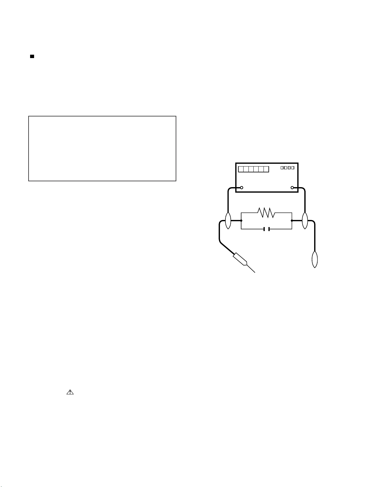
• Use an AC voltmeter having with 5000 ohm per volt, or higher, sensitivity or measure the AC voltage drop across the resistor.
• Connect the resistor connection to all exposed metal parts having a
return to the chassis (antenna, metal cabinet, screw heads, knobs
and control shafts, escutcheon, etc.) and measure the AC voltage
drop across the resistor.
All checks must be repeated with the AC cord plug connection
reversed. (If necessary, a nonpolarized adaptor plug must be used
only for the purpose of completing these checks.)
Any reading of 1.05 V peak (this corresponds to 0.7 mA peak AC.)
or more is excessive and indicates a potential shock hazard which
must be corrected before returning the monitor to the owner.
F7001, F7002 (3.15A/250V)
DVM
AC SCALE
BEFORE RETURNING THE RECEIVER
(Fire & Shock Hazard)
Before returning the receiver to the user, perform the following
safety checks:
3. Inspect all lead dress to make certain that leads are not pinched,
and check that hardware is not lodged between the chassis and
other metal parts in the receiver.
4. Inspect all protective devices such as non-metallic control knobs,
insulation materials, cabinet backs, adjustment and compartment
covers or shields, isolation resistor-capacitor networks, mechanical
insulators, etc.
5. To be sure that no shock hazard exists, check for leakage current in
the following manner.
• Plug the AC cord directly into a 220~240 volt AC outlet.
• Using two clip leads, connect a 1.5k ohm, 10 watt resistor paralleled by a 0.15µF capacitor in series with all exposed metal cabinet
parts and a known earth ground, such as electrical conduit or electrical ground connected to an earth ground.
///////////////////////////////////////////////////////////////////////////////////////////////////////////////////////////////////////////////////////////////////////////////////////////////////////////////////////////////////////////
TO EXPOSED
METAL PARTS
SAFETY NOTICE
Many electrical and mechanical parts in LCD color television have
special safety-related characteristics.
These characteristics are often not evident from visual inspection, nor
can protection afforded by them be necessarily increased by using
replacement components rated for higher voltage, wattage, etc.
Replacement parts which have these special safety characteristics are
identified in this manual; electrical components having such features
are identified by “ ” and shaded areas in the Replacement Parts
List and Schematic Diagrams.
///////////////////////////////////////////////////////////////////////////////////////////////////////////////////////////////////////////////////////////////////////////////////////////////////////////////////////////////////////////
For continued protection, replacement parts must be identical to those
used in the original circuit.
The use of a substitute replacement parts which do not have the same
safety characteristics as the factory recommended replacement parts
shown in this service manual, may create shock, fire or other hazards.
1.5k ohm
10W
0.15µF
TEST PROBE
CONNECT TO
KNOWN EARTH
GROUND
i
Page 3
LC-32DH57E/RU/S (1st Edition)
Precautions for using lead-free solder
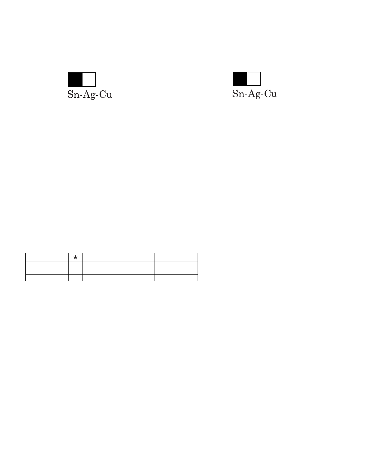
Employing lead-free solder
• “PWBs” of this model employs lead-free solder. The LF symbol indicates lead-free solder, and is attached on the PWBs and service manuals. The
alphabetical character following LF shows the type of lead-free solder.
Example:
L Fa
Indicates lead-free solder of tin, silver and copper.
Indicates lead-free solder of tin, silver and copper.
L F a/a
Using lead-free wire solder
• When fixing the PWB soldered with the lead-free solder, apply lead-free wire solder. Repairing with conventional lead wire solder may cause damage or accident due to cracks.
As the melting point of lead-free solder (Sn-Ag-Cu) is higher than the lead wire solder by 40 °C, we recommend you to use a dedicated soldering
bit, if you are not familiar with how to obtain lead-free wire solder or soldering bit, contact our service station or service branch in your area.
Soldering
• As the melting point of lead-free solder (Sn-Ag-Cu) is about 220 °C which is higher than the conventional lead solder by 40 °C, and as it has poor
solder wettability, you may be apt to keep the soldering bit in contact with the PWB for extended period of time. However, Since the land may be
peeled off or the maximum heat-resistance temperature of parts may be exceeded, remove the bit from the PWB as soon as you confirm the
steady soldering condition.
Lead-free solder contains more tin, and the end of the soldering bit may be easily corroded. Make sure to turn on and off the power of the bit as
required.
If a different type of solder stays on the tip of the soldering bit, it is alloyed with lead-free solder. Clean the bit after every use of it.
When the tip of the soldering bit is blackened during use, file it with steel wool or fine sandpaper.
• Be careful when replacing parts with polarity indication on the PWB silk.
Lead-free wire solder for servicing
Part No. Description Code
ZHNDAi123250E J φ0.3mm 250g (1roll) BL
ZHNDAi126500E J φ0.6mm 500g (1roll) BK
ZHNDAi12801KE J φ1.0mm 1kg (1roll) BM
ii
Page 4
LC-32DH57E/RU/S (1st Edition)
End of life disposal
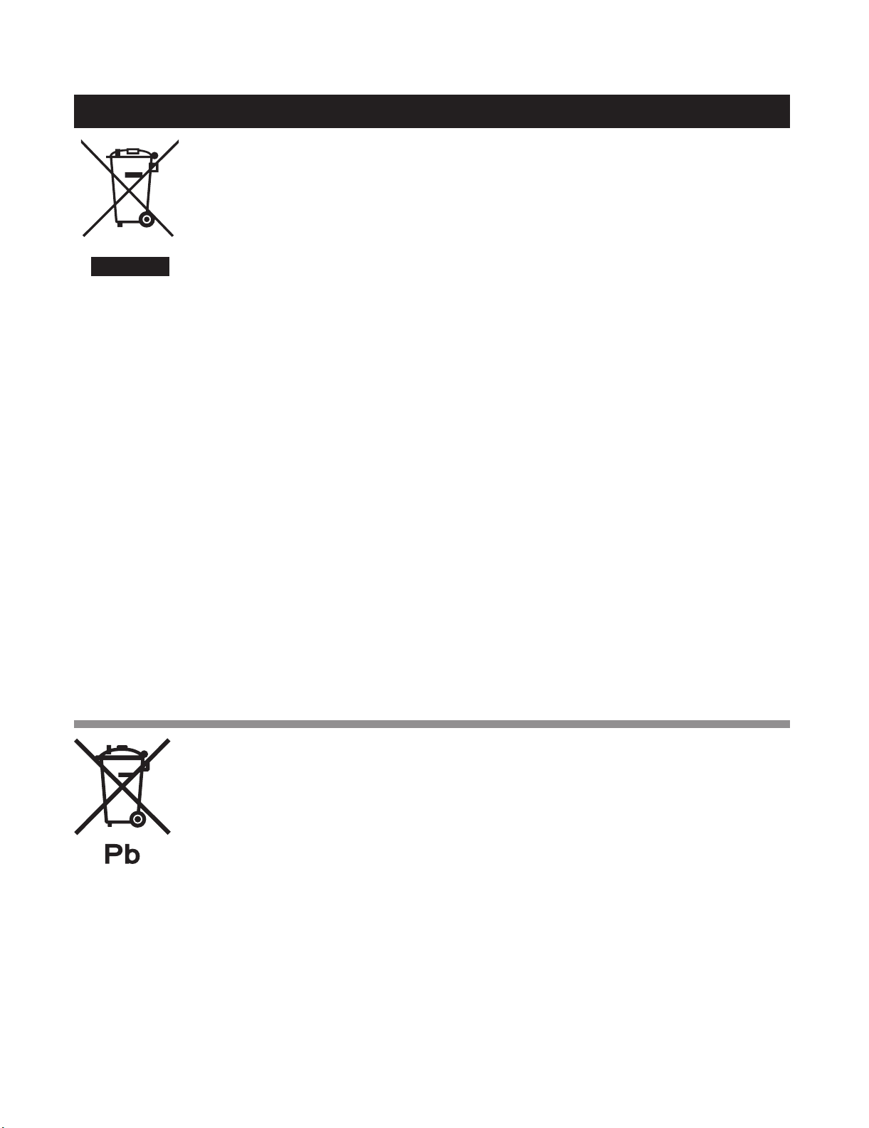
End of life disposal
A. Information on Disposal for Users (private households)
1. In the European Union
Attention: If you want to dispose of this equipment, please do not use the ordinary dust bin!
Used electrical and electronic equipment must be treated separately and in accordance with legislation that
requires proper treatment, recovery and recycling of used electrical and electronic equipment.
Following the implementation by member states, private households within the EU states may return their
used electrical and electronic equipment to designated collection facilities free of charge*. In some countries*
your local retailer may also take back your old product free of charge if you purchase a similar new one.
Attention: Your
product is marked
with this symbol.
It means that used
electrical and
electronic products
should not be
mixed with general
household waste.
There is a separate
collection system for
these products.
*) Please contact your local authority for further details.
If your used electrical or electronic equipment has batteries or accumulators, please dispose of these
separately beforehand according to local requirements.
By disposing of this product correctly you will help ensure that the waste undergoes the necessary treatment,
recovery and recycling and thus prevent potential negative effects on the environment and human health
which could otherwise arise due to inappropriate waste handling.
2. In other Countries outside the EU
If you wish to discard this product, please contact your local authorities and ask for the correct method of
disposal.
For Switzerland: Used electrical or electronic equipment can be returned free of charge to the dealer, even if
you don’t purchase a new product. Further collection facilities are listed on the homepage of www.swico.ch
or www.sens.ch.
B. Information on Disposal for Business Users
1. In the European Union
If the product is used for business purposes and you want to discard it:
Please contact your SHARP dealer who will inform you about the take-back of the product. You might be
charged for the costs arising from take-back and recycling. Small products (and small amounts) might be
taken back by your local collection facilities.
For Spain: Please contact the established collection system or your local authority for take-back of your used
products.
2. In other Countries outside the EU
If you wish to discard of this product, please contact your local authorities and ask for the correct method of
disposal.
The battery supplied with this product contains traces of Lead.
For EU: The crossed-out wheeled bin implies that used batteries should not be put to the general household
waste! There is a separate collection system for used batteries, to allow proper treatment and recycling in
accordance with legislation. Please contact your local authority for details on the collection and recycling
schemes.
For Switzerland: The used battery is to be returned to the selling point.
For other non-EU countries: Please contact your local authority for correct method of disposal of the used
battery.
iii
Page 5
LC-32DH57E-BK
CHAPTER 1. OPERATION MANUAL
[1] SPECIFICATIONS
LC-32DH57E/RU/S (1st Edition)
Service Manual
Item
LCD panel
Resolution 1,049,680 pixels (1,366 x 768)
Video Colour System PAL/SECAM/NTSC 3.58/NTSC 4.43/PAL 60
TV-Standard
TV Function
Viewing angles 176 ° (H), 176 ° (V)
Audio amplifier 10 W x 2
Speaker (35 mm x 100 mm) x 2
Terminals
OSD language
Power Requirement
Power Consumption (Method IEC62087)
Weight 10.5 kg (Without stand), 11.5 kg (With stand)
Operating temperature
Receiving Channel
TV-Tuning System
STEREO/BILINGUAL NICAM/A2
Antenna
RS-232C D-Sub 9 pin male connector
EXT 1 SCART (AV input, Y/C input, RGB input, TV output)
EXT 2 SCART (AV input/monitor output, Y/C input)
EXT 3 COMPONENT IN (Y/P
EXT 4 15 pin mini D-sub
HDMI 1 (EXT 5) HDMI
HDMI 2 (EXT 6) HDMI
HDMI 3 (EXT 7) HDMI
EXT 8 RCA pin (AV input)
SERVICE USB
HDMI 2/PC AUDIO (R/L) Ø 3.5 mm jack*
DIGITAL AUDIO OUTPUT Optical Digital audio output
C. I. (Common Interface) EN50221, R206001
OUTPUT RCA pin (AUDIO R/L)
Headphones Ø 3.5 mm jack (Audio output)
Analogue CCIR (B/G, I, D/K, L/L’)
Digital DVB-T (2K/8K OFDM)
VHF/UHF
CATV
LCDCOLOURTV(32"), LC-32DH57E, LC-32DH57RU, LC-32DH57S
Advanced Super View & BLACK TFT LCD (32")
IR A ch_E69 ch (Digital), E2_E69 ch, F2_F10 ch, I21_I69 ch, IR A_IR J ch
Hyper-band, S1_S41 ch
Auto Preset 999 ch (non-Nordic [DTV]), Auto Preset 9999 ch (Nordic [DTV]), Auto Preset 99 ch
(ATV), Auto Label, Auto Sort
UHF/VHF 75
Czech, Danish, Dutch, English, Estonian, Finnish, French, German, Greek, Hungarian, Italian,
Latvian, Lithuanian, Norwegian, Polish, Portuguese, Russian, Slovak, Slovene, Spanish, Swedish,
Turkish, Ukrainian
AC 220-240 V,50 Hz
90 W (0.6 W Standby)
0°Cto+40°C
Ω
Din type (Analogue & Digital)
B(CB
)/PR(CR), RCA pin (AUDIO R/L))
*
The HDMI 2 and EXT 4 terminals can both use the same audio input terminal.
•
As a part of our policy of continuous improvement, SHARP reserves the right to make design and specification changes for product
improvement without prior notice. The performance specification figures indicated are nominal values of production units. There may be
some deviations from these values in individual units.
NOTE
Refer to the inside back cover for dimensional drawings.
•
Optional accessory
The listed optional accessory is available for this LCD
colour TV. Please purchase them at your nearest shop.
Additional optional accessories may be available in the near
•
future. When purchasing, please read the newest catalogue for
compatibility and check the availability.
1 – 1
No. Part name Part number
Wall mount bracket (LC-
1
32DH57E, LC-32DH57RU,
LC-32DH57S)
AN-37AG5
Page 6
LC-32DH57E/RU/S (1st Edition)
[2] OPERATION MANUAL
TV (Front view)
1 2 3
TV (Rear view)
1
2
7
3
8 9
Remote control sensor
1
OPC sensor
4
5
6
7
2
3
4
5
6
7
8
(Standby/On indicator)
(Power button)
MENU (Menu button)
(Input source button)
P/ (Programme [channel]
buttons)
+/- (Volume buttons)
8
COMMON INTERFACE slot
1
SERVICE terminal (USB terminal
2
for service personnel only)
HDMI 3 (HDMI) terminal
3
EXT 8 terminals
6
10
4
Headphones
5
AC INPUT terminal
6
EXT 4 (ANALOGUE RGB)
7
terminal
HDMI 1 (HDMI) terminal
8
HDMI 2 (HDMI) terminal
9
Antenna terminal
10
HDMI 2/PC AUDIO (R/L) jack*
11
DIGITAL AUDIO OUTPUT
12
terminal
RS-232C terminal
13
EXT 3 (COMPONENT/AUDIO)
14
terminals
EXT 1 (RGB) terminal
15
EXT 2 (AV) terminal
16
OUTPUT (AUDIO) terminals
17
4
11
12
5
13
WARNING
Excessive sound pressure from earphones
•
and headphones can cause hearing loss.
•
Do not set the volume at a high level.
Hearing experts advise against extended
listening at high volume levels.
The SERVICE terminal is reserved only
•
for qualified service personnel. Do not
connect anything to the terminal.
14 15 16 17
The HDMI 2 and EXT 4 terminals can both use the same audio input terminal (HDMI 2/PC AUDIO (R/L)). However, the
*
proper item must be selected in the “PC Audio Select” menu.
1 – 2
Page 7
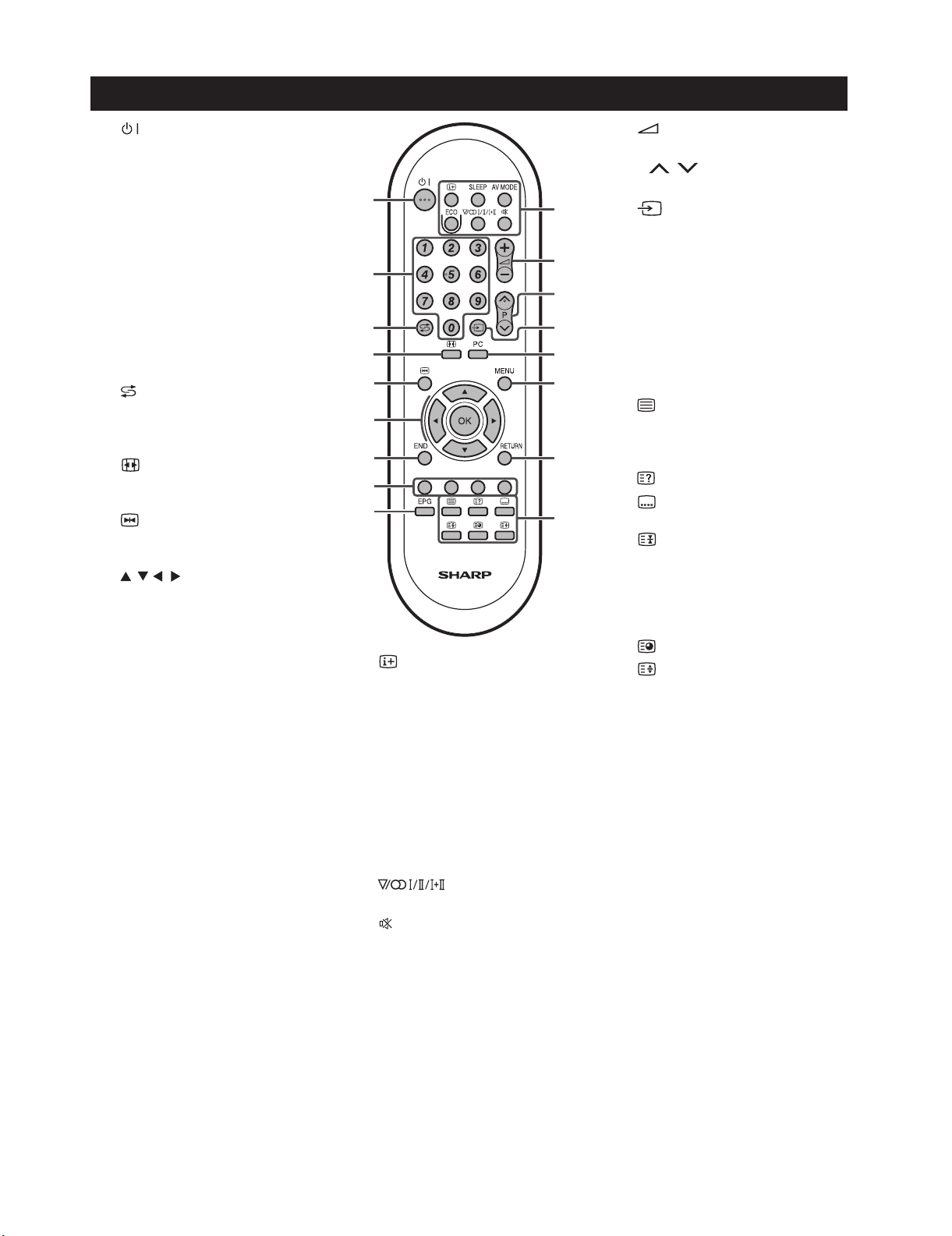
Remote control unit
LC-32DH57E/RU/S (1st Edition)
1
2
3
4
5
6
7
8
9
(Standby/On)
Numeric buttons 0-9
Set the channel.
Enter desired numbers.
Set the page in teletext mode.
When the five Nordic countries
•
(Sweden, Norway, Finland,
Denmark, or Iceland) are
selected in the country setting
from “Auto Installation”, DTV/A
TV channels are four digits.
When another country is
selected, DTV/ATV channels
are three digits.
(Flashback)
Press to return to the previously
selected channel or external
input.
(WIDE MODE)
Select a wide mode.
(Freeze)
Press to freeze a moving image
on the screen.
/ / / (Cursor)
Select a desired item on the
setting screen.
OK
Execute a command within the
“MENU” screen.
TV: Display the programme list
when no other “MENU” screen
is running.
END
Exit the “MENU” screen.
Colour (Red/Green/Yellow/
Blue) buttons
The coloured buttons are
correspondingly used to select
the coloured items on the screen
(e.g., EPG, MHEG-5, Teletext).
EPG
TV: Display the EPG screen.
1
2
3
4
5
6
7
8
9
10
(Display information)
Press to display the station
information (channel number,
signal, etc.) in the upper right
corner of the screen.
SLEEP
Press to schedule a time for the
TV to automatically standby.
AV MODE
Select a video setting.
ECO (Off/Standard/Advanced)
Select “Energy Save” setting.
(Sound mode)
Select a sound multiplex mode.
(Mute)
TV sound on/off.
10
11
12
13
14
15
16
17
11
12
13
14
15
16
17
+/- (Volume)
Increase/decrease TV volume.
P/
Select the TV channel.
(INPUT SOURCE)
Select an input source.
PC
Directly select EXT 4.
MENU
“MENU” screen on/off.
RETURN
Return to the previous “MENU”
screen.
Buttons for useful operations
(Teletext)
ATV: Display analogue teletext.
DTV: Select MHEG-5 and teletext
for DTV.
(Reveal hidden Teletext)
(Subtitle)
Switch subtitle languages on/off.
(Freeze/Hold)
Press to freeze a moving image
on the screen.
Teletext: Stop updating teletext
pages automatically or release
theholdmode.
(Subpage)
(Top/Bottom/Full)
Set the area of magnification in
teletext mode.
1 – 3
Page 8
LC-32DH57E/RU/S (1st Edition)
Attaching the stand unit
Before attaching (or detaching) the stand, unplug the AC cord from the AC INPUT terminal.
•
Before performing work, spread cushioning over the surface on which you will be laying the TV. This will prevent it
•
from being damaged.
CAUTION
•
Attach the stand in the correct direction.
•
Be sure to follow the instructions. Incorrect installation of the stand may result in the TV falling over.
Confirm that there are four screws with the
1
stand unit.
2
Place the stand unit onto the supporting
post on the bottom of the TV ( ).
Inserting the batteries
Before using the TV for the first time, insert two supplied “AA” size zinc-carbon batteries. When the batteries become
depleted and the remote control unit fails to operate, replace the batteries with new “AA” size batteries.
Open the battery cover.
1
2
Insert two supplied “AA” size batteries.
Place batteries with their terminals corresponding to the (+)
•
and (-) indications in the battery compartment.
Close the battery cover.
3
CAUTION
Improper use of batteries can result in chemical leakage or explosion. Be sure to follow the instructions below.
Do not mix batteries of different types. Different types of batteries have different characteristics.
•
Do not mix old and new batteries. Mixing old and new batteries can shorten the life of new batteries or cause chemical leakage in old
•
batteries.
•
Remove batteries as soon as they have worn out. Chemicals that leak from batteries can cause a rash. If you find any chemical leakage,
wipe thoroughly with a cloth.
•
The batteries supplied with this product may have a shorter life expectancy due to storage conditions.
If you will not be using the remote control unit for an extended period of time, remove the batteries from it.
•
Insert and tighten the four screws on the
3
bottom of the stand unit as shown ( ).
NOTE
To detach the stand unit, perform the steps in reverse order.
•
A screw driver is not supplied with this product.
•
Using the remote control unit
Use the remote control unit by pointing it towards the remote control sensor. Objects between the remote control unit
and sensor may prevent proper operation.
5m5m
30° 30°
Remote control sensor
Cautions regarding the remote control unit
Do not expose the remote control unit to shock. In addition, do not expose the remote
•
control unit to liquids, and do not place in an area with high humidity.
•
Do not install or place the remote control unit under direct sunlight. The heat may cause
deformation of the unit.
•
The remote control unit may not work properly if the remote control sensor of the TV is
under direct sunlight or strong lighting. In such cases, change the angle of the lighting or
the TV, or operate the remote control unit closer to the remote control sensor.
1 – 4
Page 9
LC-32DH57E/RU/S (1st Edition)
Troubleshooting
Problem Possible Solution
No power.•
The TV cannot be operated.•
Remote control unit does not operate.•
Picture is cut off.• Is the image position correct?
Strange colour, light colour, or dark colour,
• Adjust the picture tone.
or colour misalignment.
Power is suddenly turned off.• The TV’s internal temperature has increased. Remove any objects blocking the vent or clean.
No picture.•
No sound.• Is the volume too low?
The TV sometimes makes a cracking
•
sound.
•
Check if you pressed on the remote control unit. If the indicator on the TV lights up red, press .
•
Is the AC cord disconnected?
•
Check if you pressed on the TV.
External influences such as lightning, static electricity, etc., may cause improper operation. In this case, operate
•
the TV after first turning off the power, or unplugging the AC cord and re-plugging it in after one or two minutes.
•
Are batteries inserted with polarity (+, -) aligned?
•
Are batteries worn out? (Replace with new batteries.)
•
Are you using it under strong or fluorescent lighting?
•
Is a fluorescent light illuminating to the remote control sensor?
•
Are screen mode adjustments (WIDE MODE) such as picture size made correctly?
•
•
Is the room too bright? The picture may look dark in a room that is too bright.
•
Check the “Colour System” setting.
•
•
•
Is sleep timer set? Set to “Off” by pressing SLEEP on the remote control unit.
•
Is “No Signal Off” or “No Operation Off” activated?
•
Are connections to external equipment correct?
•
Is the correct input source selected?
•
Is a non-compatible signal being input?
•
Is the picture adjustment correct?
•
Is the antenna connected properly?
•
Is “On” selected in “Audio Only”?
•
Make sure that headphones are not connected.
•
Check if you pressed on the remote control unit.
•
•
Is the proper item selected in the “PC Audio Select” menu when connecting devices to the HDMI 2 terminal or
the EXT 4 terminal?
This is not a malfunction. This happens when the cabinet slightly expands and contracts according to changes
•
in temperature. This does not affect the TV’s performance.
Cautions regarding use in high and low temperature environments
When the TV is used in a low temperature space (e.g., room, office), the picture may leave trails or appear slightly delayed. This is not
•
a malfunction, and the TV will recover when the temperature returns to normal.
Do not leave the TV in a hot or cold location. Also, do not leave the TV in a location exposed to direct sunlight or near a heater, as this
•
may cause the cabinet to deform and the LCD panel to malfunction.
Storage temperature: + 5 °C to + 35 °C.
Information on the software license for this product
Software composition
The software included in this product is comprised of various software components whose individual copyrights are held by SHARP or by
third parties.
Software developed by SHARP and open source software
The copyrights for the software components and various relevant documents included with this product that were developed or written
by SHARP are owned by SHARP and are protected by the Copyright Act, international treaties, and other relevant laws. This product also
makes use of freely distributed software and software components whose copyrights are held by third parties. These include software
components covered by a BSD-like License or other license agreement.
We are unable to answer any questions about the source code for the open source software. The source code for the software
components whose copyrights are held by SHARP is not distributed.
Acknowledgements
The following open source software components are included in this product:
• Freetype • unicode • Teletext font • libpng • zlib
1 – 5
Page 10
LC-32DH57E/RU/S (1st Edition)
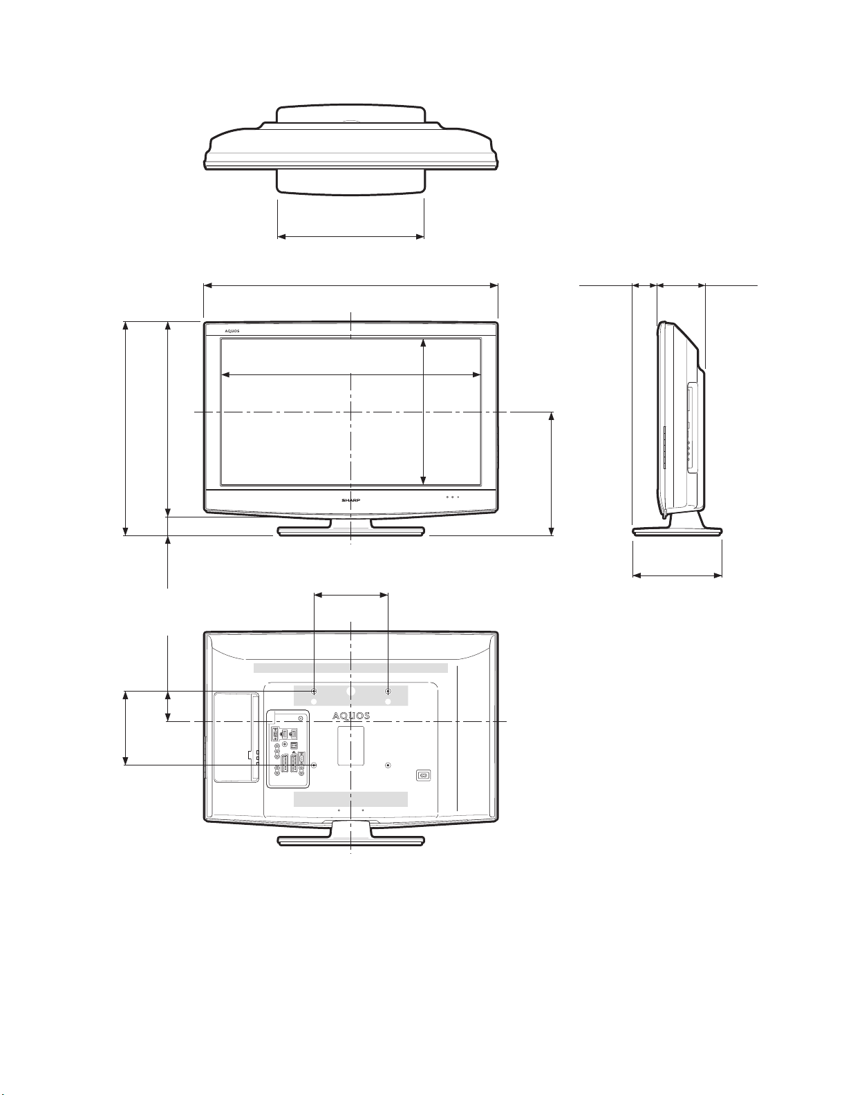
[3] DIMENSIONS
Unit: mm
390.0
390,0
575.0
575,0
528.0
528,0
47.0
47,0
791.0
791,0
699.2
699,2
200.0
200,0
393.8
393,8
333.5
333,5
66.2
66,2
123.5
123,5
235.0
235,0
200.0
200,0
82.0
82,0
1 – 6
Page 11
LC-32DH57E-BK
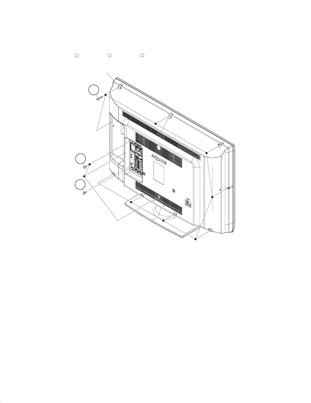
CHAPTER 2. REMOVING OF MAJOR PARTS
Service Manual
[1] REMOVING OF MAJOR PARTS
1. Removing of Rear Cabinet Ass’y.
1. Remove the 1 lock screw , 3 lock screws , 9 lock screws and detach the Rear Cabinet Ass’y.
1
2
3
Rear Cabinet Ass'y
3
LC-32DH57E/RU/S (1st Edition)
2
1
2 – 1
Page 12
LC-32DH57E/RU/S (1st Edition)
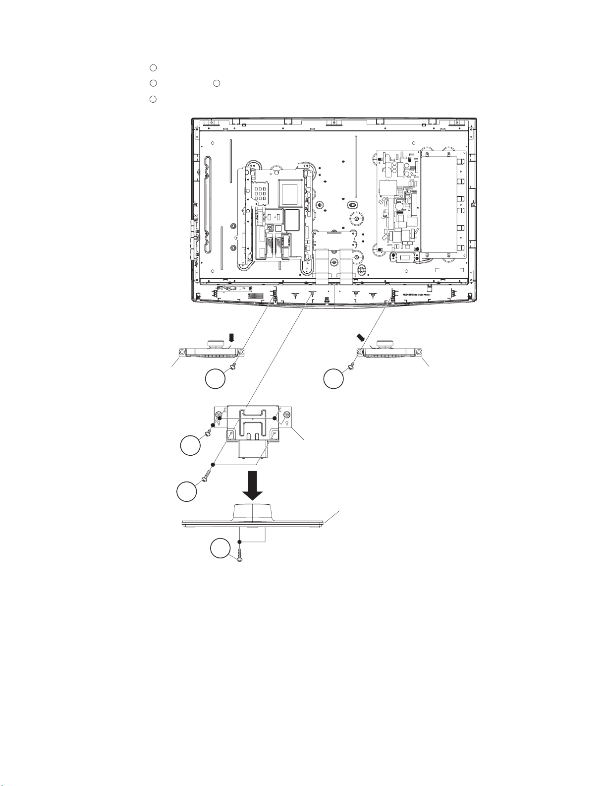
2. Removing of Connectors, Speakers, Stand Angle Ass’y and Stand Ass’y.
1. Remove all the connectors from all the PWBs.
2. Remove the 2 lock screws and detach the Speaker-L and Speaker-R.
3. Remove the 2 lock screws , 4 lock screws and detach the Stand Angle Ass’y.
4. Remove the 2 lock screws and detach the Stand Ass’y.
1
2
4
3
Speaker-R
[SP] [SP]
1
3
Stand Angle Ass'y
1
Speaker-L
2
Stand Ass'y
4
2 – 2
Page 13
LC-32DH57E/RU/S (1st Edition)
4
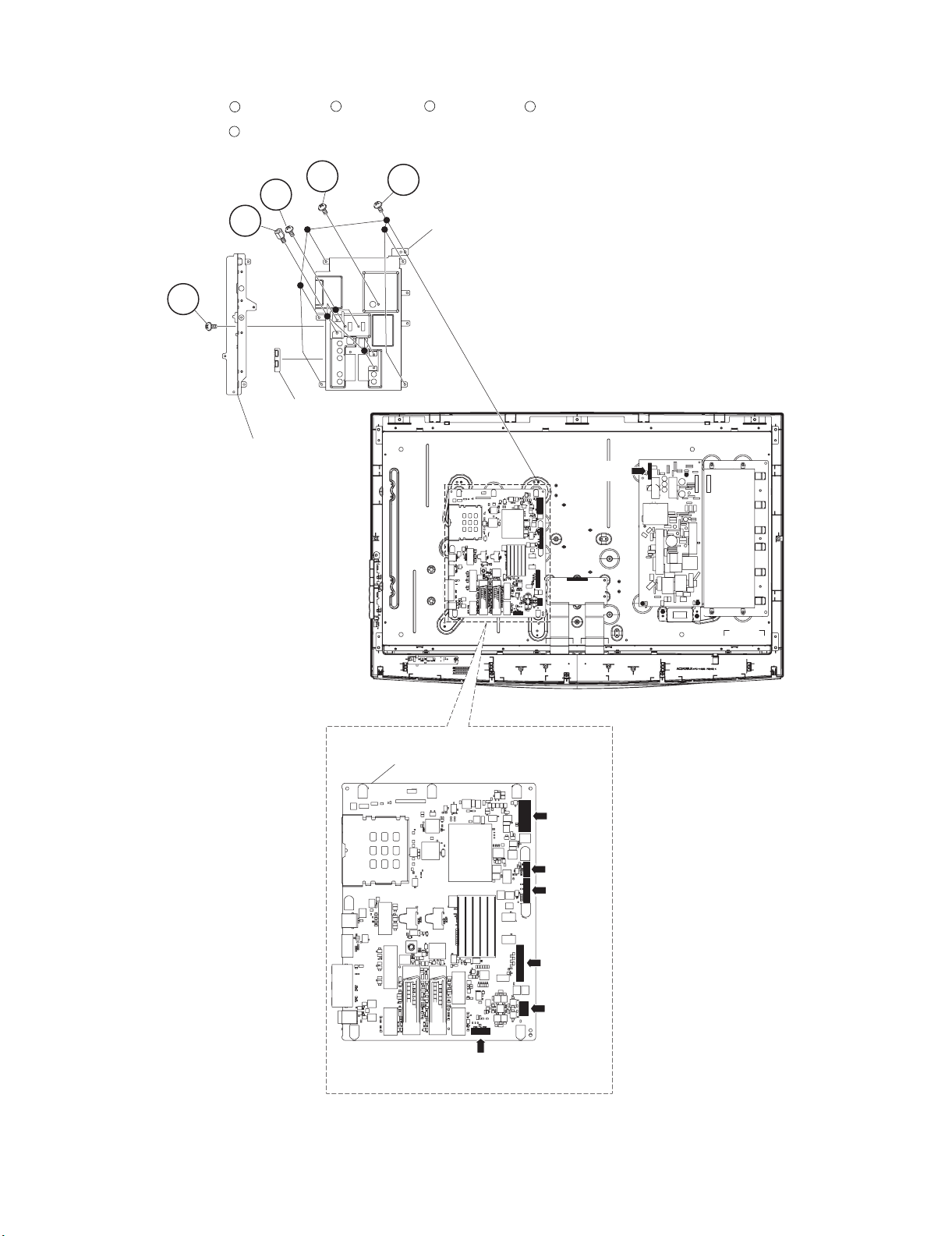
3. Removing of Main PWB Shield and AV Cover Ass’y.
1. Remove all the connectors from all the PWBs.
2. Remove the 4 lock screw , 2 lock screws , 1 lock screw , 6 lock screws and detach the Main PWB Shield.
3. Remove the 1 lock screw and detach the AV Cover Ass’y.
1
5
2
3
1
5
Earth Plate
AV Cover Ass'y
3
4
2
Main PWB Shield
[PD/LB]
Main PWB
[PD]
[LB]
[LP]
[LW]
[SP]
[RA/KM]
2 – 3
Page 14
LC-32DH57E/RU/S (1st Edition)
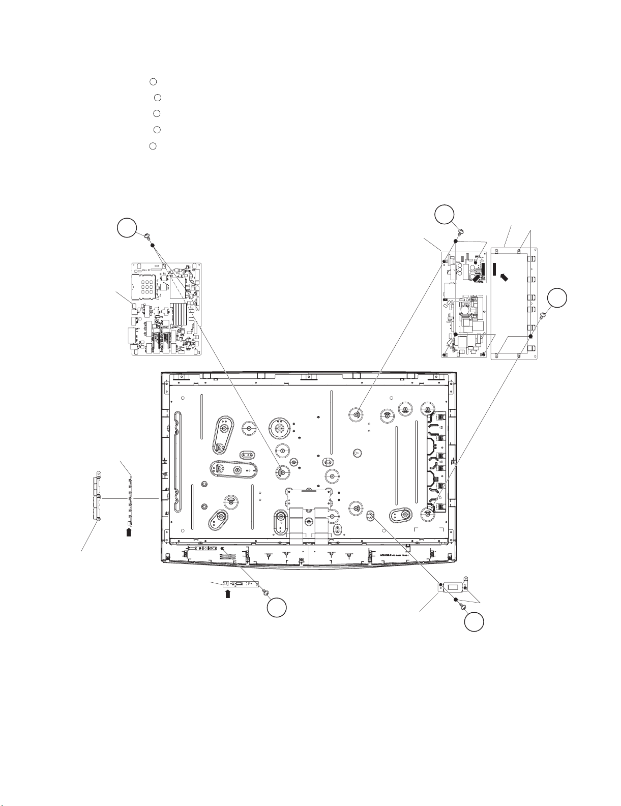
4. Removing of LED Unit, MAIN Unit, POWER Unit, INVERTER Unit, AC Inlet Angle, Control Button and KEY
Unit.
1. Remove all the connectors from all the PWBs.
2. Remove the 1 lock screw and detach the LED Unit.
3. Remove the 2 lock screws and detach the MAIN Unit.
4. Remove the 4 lock screws and detach the POWER Unit.
5. Remove the 3 lock screws and detach the INVERTER Unit.
6. Remove the 2 lock screw and detach the AC Inlet Angle.
7. Remove the Control Button.
8. Remove the KEY Unit.
1
2
3
4
5
MAIN Unit
KEY Unit
3
2
POWER Unit
INVERTER Unit
[BtoB][BtoB]
4
[KM]
Control Button
LED Unit
[RA]
1
AC Inlet Angle
2 – 4
5
Page 15
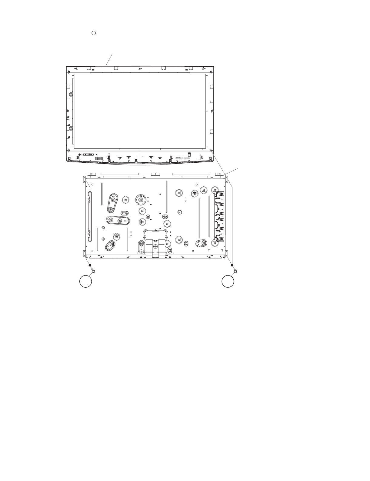
5. Removing of 32” LCD Panel Module.
1. Remove the 4 lock screws and detach the 32” LCD Panel Module from Front Cabinet.
1
Front Cabinet Ass'y
LC-32DH57E/RU/S (1st Edition)
32" LCD Panel Module
11
2 – 5
Page 16
LC-32DH57E/RU/S (1st Edition)
LC-32DH57E-BK
CHAPTER 3. ADJUSTMENT PROCEDURE
Service Manual
[1] ADJUSTMENT PROCEDURE
1. Adjustment method after PWB and/or IC replacement due to repair
The unit is set to the optimum at the time of shipment from the factory. If any value should become improper or any adjustment is necessary due to
the part replacement, make an adjustment according to the following procedure.
1. Procure the following units in order to replace the main unit, E2PROM (IC8455).
MAIN UNIT: DUNTKF111FM08
NOTE: [Caution when replacing ICs in the main unit (IC501)]
The above ICs are EEPROMs storing the EDID data of PC data.
Before replacing the relevant part, procure the following parts in which the data have been rewritten.
IC501 RH-iXC206WJQZS EDID (PC) ANALOG-RGB
2. Entering and exiting the adjustment process mode
1. Press the “MAIN POWER” key on the set of running TV set to force power off.
(Or, unplug the AC power cord of running TV set to force power off.)
2. While holding down the “ (-)” and “INPUT” keys on the set at once, press the “MAIN POWER” key on the set to turn on the power.
The letter “K” appears on the screen.
3. Next, hold down the “ (-)” and “P ( )” keys on the set at once.
Multiple lines of orange characters appearing on the screen indicate that the set is now in the adjustment process mode.
If you fail to enter the adjustment process mode (the display is the same as normal start up), retry the procedure.
4. To exit the adjustment process mode after the adjustment is done, press the MAIN POWER key and turn off a power supply. or unplug the AC
power cord to force power off.
(When the power is turned off with the remote controller, once unplug the AC power cord and wait for 10 seconds before plug it in again.)
CAUTION: Use due care in handling the information described here lest the users should know how to enter the adjustment process mode.
If the settings are tampered with in this mode, unrecoverable system damage may result.
3. Remote controller key operation in adjustment process mode.
1. key operation
Remote controller key Main unit key Remote controller key Main unit key Function
P (/) P (/)
(+/-) (+/-)
Cursor ( / ) — Turning a page (PREVIOUS/NEXT)
Cursor ( / ) — Changing a selected line setting (+10/-10)
Input button Input button
OK — Executing a function
Input mode is switched automatically when relevant adjustment is started so far as the necessary input signal is available.
Moving an item (line) by one (UP/DOWN)
Changing a selected item setting (+1/-1)
Input source switching (toggle switching)
(TV→EXT1→EXT2→EXT3→EXT4→HDMI1→HDMI2→HDMI3→EXT8)
3 – 1
Page 17
LC-32DH57E/RU/S (1st Edition)
4. Description of display
(1) Current page / Total pages (2) Currentry selected input
(3) Inch setting and Model name display
PAGE 1/7 TV 32E_DH57E Adjustment process menu header
Main Version 1.14
Boot Version 20090429.1.12
T-CON Version 00 00 00 00 32 4C 32 B1
INCH SIZE xx
ERROR RESET NO [NO/YES]
STANDBY CAUSE 00 00 00 00 00
(4) Item name (5) Parameter
No. Description Display specification
(1) Current page/total pages 2char/2char Decimal Number mark.
(2) Currentry selected input TV→EXT1→EXT2→EXT3→EXT4→HDMI1→HDMI2→HDMI3→EXT8
(3) Inch setting and destination display 32
(4) Item name Max. 30 char
(5) Parameter table Max. 60 char (Preset value of each item)
[1] 00H 00M
[2] 00H 00M
[3] 00H 00M
[4] 00H 00M
[5] 00H 00M
3 – 2
Page 18
LC-32DH57E/RU/S (1st Edition)
5. Adjustment process mode menu
The character string in brackets [ ] will appear as a page title in the adjustment process menu header.
Page Line Item Description Remarks (adjustment detail, etc.)
1/7
1 Main Version 1.14 Main microprocessor version
2 Boot Version 20090429.1.12 Boot version of the main microprocessor
3 T-CON Version 00 00 00 00 32 4C 32 B1 T-CON microprocessor version
4 INCH SIZE 32 Initial Setting of panel size
5 ERROR RESET NO [NO/YES] Lamp error reset. (Select “YES” and press “OK” key.)
6 STANDBY CAUSE 00 00 00 00 00 Error standby cause. Total operating time before error.
1) 00H 00M (5 times histories)
2) 00H 00M
3) 00H 00M
4) 00H 00M
5) 00H 00M
2/7
1 INDUSTRY INIT [NO/YES(E)/YES(I)/YES(F)/YES(R) Initialization to factory settings execution.
2 PUBLIC MODE OFF [OFF/ON] ON/OFF setting of hotel mode
3 I2C DATA 000000000000 Write and read of data in I2C BUS control IC.
4 I2C STATE WAIT [STANDBY/WAIT] Execution of write and read of I2C DATA
3/7
1 INSPECT USB TERM ENTER Reading inspection of USB memory terminal
2 HDMI CEC TEST ENTER HDMI CEC test
4/7
1 VIDEO ADJ ENTER VIDEO level adjustment execution
2 CHANNEL E-9
3 GAIN 31 Gain adjustment
4 ADJ RESET NO [NO/YES] Reset of adjustment
5/7
1 COM-ADJ ENTER COMPONENT level adjustment execution
2 Y OFF SET 70 Y CUTOFF adjustment value
3 PB OFF SET 128 PB CUTOFF adjustment value
4 PR OFF SET 128 PR CUTOFF adjustment value
5 Y GAIN 140 Y GAIN adjustment value
6 PB GAIN 140 PB GAIN adjustment value
7 PR GAIN 140 PR GAIN adjustment value
8 ADJ RESET NO [NO/YES] Reset of adjustment
6/7
1 RGB-ADJ ENTER SCART RGB level adjustment execution
2 R OFF SET 128 R OFF SET adjustment value
3 G OFF SET 128 G OFF SET adjustment value
4 B OFF SET 128 B OFF SET adjustment value
5 R GAIN 80 R DRIVE adjustment value
6 G GAIN 80 G DRIVE adjustment value
7 B GAIN 80 B DRIVE adjustment value
8 ADJ RESET NO [NO/YES] Reset of adjustment
7/7
1 COM BIAS 67 Common Bias auto adjustment execution
2 LCD TEST PATTERN 0 Pattern with built-in LCD controller display
3 WB Point A 500 W/B adjustment, gradation Point A input setting
4 Point B 3500 W/B adjustment, gradation Point B input setting
5 Point A ADJ R 520 W/B adjustment, gradation Point A R_adjustment value
6 ADJ G 500 W/B adjustment, gradation Point A G_adjustment value
7 ADJ B 380 W/B adjustment, gradation Point A B_adjustment value
8 Point B ADJ R 3500 W/B adjustment, gradation Point B R_adjustment value
9 ADJ G 3500 W/B adjustment, gradation Point B G_adjustment value
10 ADJ B 3160 W/B adjustment, gradation Point B B_adjustment value
11 WB WRITE NO [NO/YES] W/B writing of adjustment values
12 WB RESET NO [NO/YES] Reset of W/B adjustment value
3 – 3
Page 19

LC-32DH57E/RU/S (1st Edition)
6. Special features
1. STANDBY CAUSE (Page 1/7)
Display of a cause (code) of the last standby.
The cause of the last standby is recorded in EEPROM whenever possible.
Checking this code will be useful in finding a problem when you repair the troubled set.
7. ROM Writing (HDMI_EDID)
1. EDID writing
1) Get ready the PC with COM port (RS-232C) running on Windows 95/98/ME/2000/XP operating system, as well as the RS-232C cross cable.
2) Start the set with the set connected with the personal computer with the RS232C cross cable.
3) Start the terminal software. (The freeware readily available on the Internet will do.)
4) Make the following settings.
Baud rate : 9600 bps
Data LENGTH : 8bit
Parity bit : none
Stop bit : 1 bit
Flow control : none
5) Input following commands to terminal software.
“KRSW0001”
PC replies “ERR” (you should ignore this replay)
“KKT10037”
PC replies “OK”
“WRED0000”
PC replies “OK” ... At that time, EDID writing finish with succeess.
6) It usually returns to a state by AC-OFF/ON.
Disconnect and connect AC cable, then TV wakes up with normal mode.
2. Software version
(1) Mainmicon Software Ver. 1.14 *1
(2) Boot version of mainmicon Software Ver. 1.12 *1
(3) T-CON Monitor micon Software Ver. 1.0 *1
*1 Please refer to the change report document for the latest version (Issued it to SEES).
3 – 4
Page 20
LC-32DH57E/RU/S (1st Edition)
8. Adjustment procedure
1. Inch Setting
Adjustment point Adjustment conditions Adjustment procedure
1 Inch Setting Adjustment process mode
Adjustment process
“INCH SIZE” menu page 1/7
2. COMB-BIAS Adjustment
Adjustment point Adjustment conditions Adjustment procedure
1 COM-BIAS Adjustment A visual check
Adjustment process
“COM BIAS” menu page 7/7
1) Inch Setting with adjustment process mode.
2) Enter the adjustment process mode, refering to the 2nd item.
3) By using P ( / ) key of R/C, Move the cursor to “INCH SIZE” on page 1/
7.
4) Select inch size 32 with the Volume (+)/(-) key of remote control.
5) Press the “OK” key of remote control.
6) After a while, If “*** OK ***” is displayed, the setting is completed.
1) COM-BIAS Adjustment with adjustment process mode.
2) Enter to the adjustment process mode, refering to the 2nd item.
3) By using / key and P ( / ) key of R/C, Move the cursor to “COMBIAS” on page 7/7.
4) Press the “OK” key. then, you can check that the pattern for adjustment is
displayed.
5) Adjust so that the flicker for the central part of a screen becomes the minimum using the volume (+)/(-) key of R/C.
6) In order to exit from this process, press the “OK” key of remote control again.
3 – 5
Page 21
LC-32DH57E/RU/S (1st Edition)
[In-house signal E12CH]
9. Video signal adjustment procedure
* The adjustment process mode menu is listed in 5th item.
Signal generator level adjustment check (Adjustment to the specified level)
• Composite signal PAL/SECAM : 0.7Vp-p ± 0.02Vp-p (White level from pedestal)
• PC (Analog D_sub15pin) signal : 0.7Vp-p ± 0.02Vp-p (White level from pedestal)
• 33K component signal : Y level 0.7Vp-p ± 0.02Vp-p (White level from pedestal)
: PB,PR level 0.7Vp-p ± 0.02Vp-p
1. Picture Adjustment
1) Entering the adjustment process mode
Adjustment point Adjustment conditions Adjustment procedure
Enter to the adjustment process mode, refering to the 2nd item.
2) TUNER adjustment
Adjustment point Adjustment conditions Adjustment procedure
1 Setting [Signal]
PAL split colour Bar
In-house UV
[Terminal]
TUNER
• Feed the In-house signal (PAL color bar) to TUNER.
• Make sure the PAL colour bar pattern has the sync level of 7:3 with the picture level.
• Feed the SMPTE color bar signal to TUNER.
JABIL: 203.25MHz
2 Auto adjustment
performance
3) ADC adjustment (Component 33K)
Adjustment point Adjustment conditions Adjustment procedure
1 Setting [Signal]
2 Auto adjustment
performance
4) PC signal adjustment (Analog D-SUB15pin)
Adjustment point Adjustment conditions Adjustment procedure
1 Setting [Signal]
Adjustment process
[VIDEO ADJ] menu page 4/7
COMP 33K 50Hz 100% Full field
colour bar
[Terminal]
EXT3 CONPONENT input
Adjustment process [COM ADJ]
menu page 5/7
XGA 60 Hz 100% Full field
colour bar
[Terminal]
EXT4 PC input
Bring the cursor on [VIDEO ADJ] and press OK key [*** OK ***] appears when
finished.
• Feed the COMPONENT 33K 100% Full field colour bar (colour saturation
level 100%) signal to the CONPONENT video input of EXT3.
100% white Black
Bring the cursor on [COM ADJ] and press OK key [*** OK ***] appears when finished.
• Feed the XGA 60Hz 100% Full field colour bar (colour saturation level 100%)
signal to the EXT4 PC input.
100% white Black
2 Auto adjustment
performance
Adjustment process [RGB ADJ]
menu page 6/7
Bring the cursor on [RGB ADJ] and press OK key [*** OK ***] appears when finished.
3 – 6
Page 22
LC-32DH57E/RU/S (1st Edition)
10. White Balance Adjustment
Adjustment gradation values (INFO) appear on page 7/7 3-4 lines of process adjustment, and adjustment initial values (offset value) appear on pages
7/7 5-10 lines. For white balance adjustment, adjust the offset values on pages 7/7 5-10 lines.
1. Preparation
1) Luminance meter reference device :Minolta CA-210
2) Condition of the unit for adjustment and inspection :Modulated light: MAX (+16)
2. Setting
1) The luminance meter is set to the center of the screen of the set.
2) In “INCH SIZE” on the process adjustment page 1/7, sets it to the size of each panel with the / key to R/C.
3. Adjustment method
Check that the values of point A and B on page 7/7 of process adjustment are set as below. If not, change them accordingly.
WB Point A 500 WB Point B 3500
1) Display the current adjustment status at point B. (Page 7/7 of process adjustment)
The display for checking the adjustment status is toggled by pressing the “OK” button on the remote control.
(Normal OSD display → “B” → display for check (OSD disappears) → “B” → normal OSD display → ...)
2) Read the value of the luminance meter.
3) Change Point B ADJ R/Point B ADJ B (Adjustment offset value) on page 7/7 of process adjustment so that the values of the luminance meter
approach x = 0.272 and y = 0.277.
(Basically, Point B ADJ G is not changed.)
4) Follow Point A as well as item 3).
Change Point A ADJ R/Point A ADJ B (Adjustment offset value) on page 7/7 of process adjustment so that the values of the luminance meter
approach x = 0.272 and y = 0.277.
5) Select “WB WRITE” on page 7/7 in the process, set “YES”, and press the OK key of remote control.
The adjustment value is written. and then shut down the AC power.
* Initial value of RGB of point B: 3500
* Initial value of RGB of point A: based on calculated of each G point
6) [Adjustment value]
* Teaching set send by engineering dept is set as reference
4. Adjustment reference standard value
Level Spec Data Adjustment Spec Inspection Spec
Point A ref. value
Point B ref. value
Adjustment spec ± 0.004
Adjustment spec ± 0.002
500
3500
x=0.272
y=0.277
x=0.272
y=0.277
Inspection spec ± 0.006 (point 1)
Inspection spec ± 0.004 (Excluding the above-mentioned)
±0.001
±0.002
±0.002
±0.004
3 – 7
Page 23
LC-32DH57E/RU/S (1st Edition)
PAGE1/7 TV 32E_DH57E
㵘 MainVersion -
Boot Version T-CON Version INCH SIZE ERROR RESET NO
STANDBYCAUSE 0000000000
1) 00H 00M
PAGE1/7 TV 32E_DH57E
㵘 MainVersion -
Boot Version T-CON Version INCH SIZE 32
ERROR RESET NO
STANDBYCAUSE 0000000000
1) 00H 00M
11. QS Temperature NVM Data Confirmation
During servicing of the LCD TV set, by software upgrading or by any cleaning NVM, it’s mandatory select the “INCH SIZE” in Service Mode, Page 1,
according to the size of the TV set.
Default picture after cleaning NVM. Picture with [Inch Setting] to 32.䋨It is actually set as each inch.䋩
12. Initialization to factory settings
After a factory setting, It ends with the AC power supply OFF.
After a factory settings, Do not turn on the power supply. If you turn on the power supply. execute the factory settings again.
Do not do power supply OFF by remote control.
CAUTION: When the factory settings have been made, all user setting data, including the channel settings, are initialized.
(The adjustments done in the adjustment process mode are not initialized.) Keep this in mind when initializing these settings.
Adjustment item Adjustment conditions Adjustment procedure
1 Factory settings Ends in AC power supply
OFF. (See to below caution)
After adjustments, exit the adjustment process mode.
To exit the adjustment process mode, turn off the MAIN power key.
When the power is turned off with the remote control, unplug the AC power cord and plug it back in.
(wait approximately 10 seconds before plugging in the AC power cord)
[Factory setting with adjustment process mode]
• Enter the adjustment process mode.
• Move the cursor to “INDUSTRY INIT” on page 2/7.
• Use the / key of R/C to select a region from “YES (E)/YES (I)/YES (F)/YES (R)”
and press the [OK] key.
• “EXECUTING” display appears and initialization starts.
• After a while, “OK” display appears, the setting is completed.
When succeeding: The background color becomes green.
When failing: The background color becomes red.
NOTE: Never turn the power off during initialization.
When performing factory settings (while displaying page 2 of adjustment process), confirm
that the item “INCH SIZE” or the panel size displayed in the upper right corner corresponds
to each panel size.
The following items are initialized in the factory setting.
1) User settings
2) Channel data (e.g. broadcast frequencies)
3) Manufacturer option setting
4) Password data
3 – 8
Page 24
LC-32DH57E/RU/S (1st Edition)
13. Functional explanation of STANDBY CAUSE
13.1. [display method]
It is displayed in the top page of the process adjustment mode. (Page displayed first when entering process mode)
13.2. [Content of display]
1. NORMAL STANDBY CAUSE
The reason that became a power-off by the specification of usual use and the main body is displayed.
(Only the one latest) It is not displayed when power supply OFF is carried out with remote control.
Display code Display character string Reason
00 00 00 00 00 00 When based on No error
0x01 1 RC_STANDBY When based on RC Standby OFF
0x05 5 PC_OUT_OF_RANGE When based on out of range for pc OFF
0x06 6 NO_OPERATION When based on non-operated OFF
0x07 7 NO_SIGNAL When based on non-signal OFF
0x0A a SLEEP_TIMER When based on an sleep-timer OFF
0x0C c RS232C When based on the command from RS232C (standby)
0x18 18 AV_LINK When based on the command from AV-LINK (standby)
2. ERROR STANDBY CAUSE
When main CPU becomes a power-off detecting some abnormalities, the use time of the set at the time of the reason and the power-off is displayed five times.
When time information can be acquired from digital broadcasting, the date and time when the error occurs at the same time is recorded, displayed
and when time information cannot be acquired, it becomes the above-mentioned display.
“00” is displayed when abnormality has not been detected even once.
Display error code Display character string Reason
0x1A 1a TEMP_ERROR When temperature (high temperature) is abnormal.
0x1B 1b LAMP_ERROR When lamp is abnormal
0x1C 1c POWER_ERROR When power module is abnormal status.
14. Lamp error detection
1. Function description
This LCD colour television has a function (lamp error detection) to be turned OFF automatically for safety when the lamp or lamp circuit is abnormal.
If the lamp or lamp circuit is abnormal, or some other errors happen, and the lamp error detection is executed, the following occur.
1) The main unit of television is turned OFF about 5 seconds after it is turned ON.
(The power LED on the front side of TV turns from green to red.)
2) If the situation “1” happens 5 times sequentially, the power is turned on (relay is turned ON).
However, the backlight is not turned on, and then the relay is turned OFF after 5 to 6 seconds. (The power LED remains red.)
2. Countermeasures
When television is turned OFF by the lamp error detection mentioned above, it enters the adjustment process with the power LED red.
Entering the adjustment process, turns OFF the error detection and turns ON TV.
This enables the operation check to detect errors in the lamp or lamp circuit.
Check whether “STANDBY CAUSE” on line 6, page 1/7 of the adjustment process is “1B”. it indicates the lamp error detection was executed.
After confirming that the lamp or lamp circuit is normal, reset the lamp error counter pushing “OK” in the R/C.
After resetting counter the green bar appears on Screen.
3. Reset standby cause error list
After confirming that the lamp error counter has been erased, select “ERROR RESET”, page 1/7 of the adjustment process and select YES using
the right cursor. For execute press “OK” in the R/C and the label “***OK***” appears on Screen.
3 – 9
Page 25
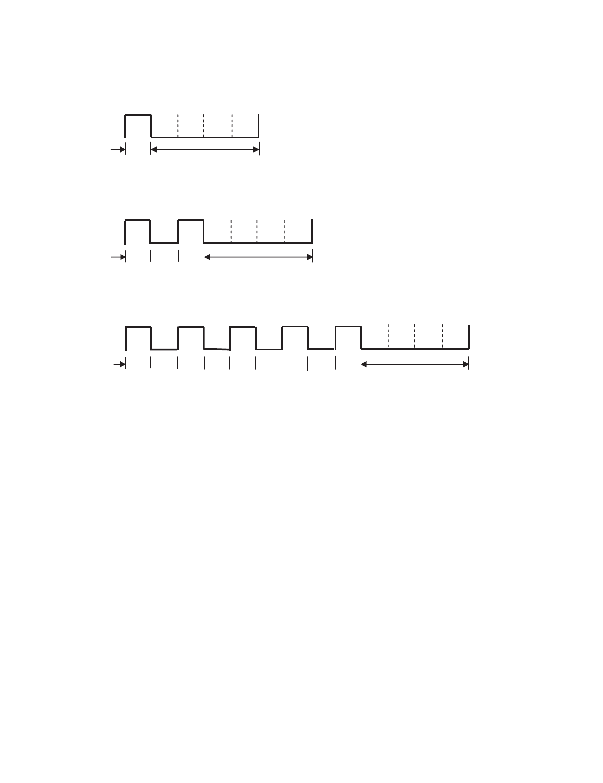
15. Blinking display when error is detected
When system received error report, Standby LED (red) blinks as follows.
POWER LED should keep dark while error indication.
1) Lamp error
Blink timing (1 blink/1 period)
Light (H)
Dark (L)
LC-32DH57E/RU/S (1st Edition)
2) Power module error
Blink timing (2 blink/1 period)
㪣㫀㪾㪿㫋㩷㩿㪟㪀
㪛㪸㫉㫂㩷㩿㪣㪀㩷
3) High temperature
Blink timing (5 blink/1 period)
Light (H)
Dark (L)
250ms
㪉㪌㪇
250 250 250 250 250
1000ms
㪉㪌㪇㪉㪌㪇
㪈㪇㪇㪇㫄㫊
250
250250250
1000ms
3 – 10
Page 26

LC-32DH57E/RU/S (1st Edition)
16. Upgrading the software
1. Unplug AC cable from outlet.
2. Insert an USB memory that is written a new software to USB port.
3. Keep pressing POWER button on LCD panel and plug AC cable to outlet.
4. POWER LED on panel automatically start blinking.
(POWER LED: Both red and green light blinking with sync. In other word, it looks, /blinking period is short ... 2 cycle - light - out - light - out / 1 sec.)
5. After a while (about 2 min.) following screen appears. Indicated percentage means progress of version up.
<SYSTEM UPGRADE>
System Version: EXXXXXXX
0%
STATUS
UPDATING...
6. After the progress becomes 100%, then STATUS area changes “UPGRADE COMPLETE” as followings (POWER LED: Only green blinks slowly ...
2 sec./time).
<SYSTEM UPGRADE>
System Version: EXXXXXXX
100%
STATUS
UPGRADE COMPLETE
* If above screen is not appeared and “UPGRADE FAILURE” is indicated in STATUS area, at that time update failure. Please repeat from step 1.
(POWER LED: Only red blinks slowly ... 2 sec./time).
OK
<SYSTEM UPGRADE>
System Version: EXXXXXXX
50%
STATUS
UPGRADE FAILURE
NG
7. Unplug AC cable from outlet.
8. Remove USB memory from USB port.
3 – 11
Page 27
LC-32DH57E-BK
CHAPTER 4. TROUBLESHOOTING TABLE
Service Manual
[1] TROUBLESHOOTING TABLE
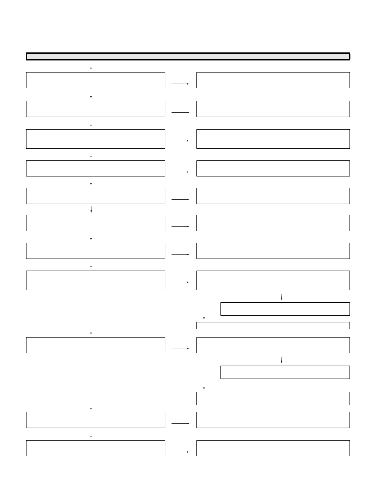
No power supplied (Front LED does not light up). No power-up even if turned on (Front LED light up)
YES
LC-32DH57E/RU/S (1st Edition)
Is the power cord connector, AC-IN harness, and PD harness
connected to the POWER unit normally?
YES
Is the connection of B to B connector between the POWER
unit and the INVERTER unit normal? (P7201-CN7302)
YES
Are F7001 (3.15A) and F7002 (3.15A) normal? NO Replace F7001 or F7002 and switch on the power again.
YES
Is DC310V supplied to the primary side capacitor C7114 and
C7108, when the power switch is turned on?
YES
Is UR12.5V supplied from pin (13) (14) of PD connector
(P7202), when the power switch is turned on?
NO Reconnect the power cord, the AC-IN harness and PD harness cor-
rectly.
NO Correct connection or the short circuit of a B to B connector nor-
mally. (P7201-CN7302)
If Fuse still blow out, check L7001, L7002, D7104, VA7001, and
VA7002.
NO Check whether there are any abnormalities in a rectification circuit.
(D7104, C7114, C7108, L7101)
YES (*1) fly to the check item of INV60V.
NO
Is about DC400V supplied to primary side capacitor C7112? NO Check whether there are any abnormalities in a power factor
YES
Check whether the PS_ON “H” signal is inputted to the pin (6)
of PD connector (P7202) in the power supply unit.
YES
Check again after remove parts which have trouble or a short
circuit. Is UR12.5V supplied from pin (13) (14) of PD connector (P7202)?
YES
After the power supply is turned on, is INV60V generated in
connector P7201 (20-23) pin? (*1)
YES
Is BU3.3V/D3.3V supplied to pin (5) (6) of RA connector
(P3301) in a main unit, and pin (1) (2) of P101 in the R/C unit?
NO Check whether the PS_ON “H” signal is outputted to pin (10) of PD
NO Is there a part which breaks down on the UR12.5V line or short-cir-
NO Is connector CN7302 of the INV unit removed, and is INV60V gener-
NO Check the power supply circuit of BU3.3V and D3.3V.
improvement circuit. (IC7101, Q7103, D7113, D7213)
connector (P9601) and pin (AC11) of IC3303 (VCT) in the MAIN unit.
culated?
NO
Check the power control circuit of UR12.5V.
(IC7201, T7206, D7217, C7220, C7222, C7228, D7215)
YES
Check again after remove parts which have trouble or a short circuit.
ated in connector P7201 (20-23) pin?
NO
Check the inverter power circuit of INV60V.
(D7227, C7221, C7223, T7206, D7220, D7221)
YES
It is failure inside an INV unit. check broken parts or a shorting part.
(Q7809, Q7807, Q7811, Q7810, etc.)
(IC9605, IC9607/IC9602, etc.)
YES
“No power supplied (Front LED does not light up)”. “No
power-up even if turned on (Front LED light up).” Is it OK?
NO Review the former step and check it again.
4 – 1
Page 28
LC-32DH57E/RU/S (1st Edition)
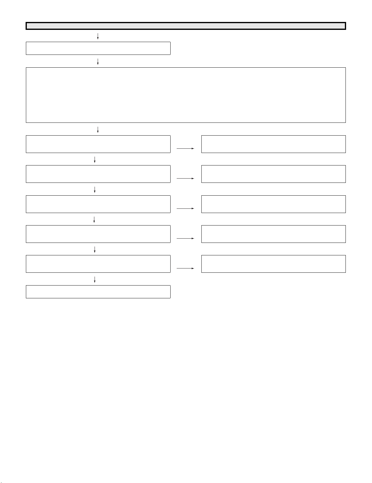
Power supply (troubleshooting): A power supply does not come to each main circuit/IC. (1)
The power supply of TUNER (TU1102) does not operate.
(IF5V)
Checklist
1) The check of the front page POW-UNIT is completed. ••• UR12.5V is output to PD (P9601) (MAIN-UNIT).
(If UR12.5V is not output, confirm the POW-UNIT again and repair.)
2) Check that STB3.3V is supplied to pin (V24) of IC3303 (included MICON), and the PS_ON signal “H” is output from (AC11) pin within a MAIN
UNIT.
(If STB3.3V is not supplied, check IC9605 (BU3.3V-REG), IC9607 (V-DET), and a peripheral circuit.)
3) Refer to attached sheet SYSTEM Block diagram.
4) Attention: The terminal of IC3303 (VCT) cannot be actually checked by hiding oneself, and check it with another terminal of the same line,
please.
Is IF5V supplied to pin (3) of TUNER (TU1102)? YES Check the soldering of TUNER (TU1102), confirm I2C-LINE or
exchange it.
NO
Is D5V output from pin (3) of IC9608 (D5V-REG)? YES Check the soldering of Q1105 and TUNER (TU1102).
NO
Is UR12.5V supplied to pin (2) of IC9608 (REG)? NO Check the pin (1) (2) of connector PD (P9601).
YES
Check whether D_POW “H” signal is input to pin (7) of IC9608? YES Check soldering IC9608 (D5V-REG) or exchange it.
NO
Check whether PS-ON “H” signal is input to pin (2) of IC3305? YES Check soldering IC3305 (V-DET) or exchange it.
NO
Check whether PS-ON “H” signal is outputted from pin (AC11) of
IC3303.
4 – 2
Page 29
LC-32DH57E/RU/S (1st Edition)
Power supply (troubleshooting): A power supply does not come to each main circuit/IC. (2)
The power supply of a VIDEO system does not operate.
(IC3303)
(BU3.3V), (D3.3V), (D1.1V), (CPU1.2V)
Checklist
1) The check of the front page POW-UNIT is completed. ••• UR12.5V is output to PD (P9601) (MAIN-UNIT).
(If UR12.5V is not output, confirm the POW-UNIT again and repair.)
2) Check that STB3.3V is supplied to pin (V24) of IC3303 (included MICON), and the PS_ON signal “H” is output from (AC11) pin within a MAIN
UNIT.
(If STB3.3V is not supplied, check IC9605 (BU3.3V-REG), IC9607 (V-DET), and a peripheral circuit.)
3) Refer to attached sheet SYSTEM Block diagram.
4) Attention: The terminal of IC3303 (VCT) cannot be actually checked by hiding oneself, and check it with another terminal of the same line,
please.
Is BU3.3V supplied to pin (V24) of IC3303 (VCT)? NO Check whether BU3.3V is outputted from pin (3) of IC9605
YES
Is D3.3V, D1.1V, and CPU1.2V supplied to pin (F18) (C6) (K12)
of IC3303 (VCT).
NO Are D3.3V, D1.1V, and CPU1.2V output from IC9602 (SW) (1)
(REG).
NO
Check whether the voltage detection signal input from IC9607 (VDET) (1) pin to IC9605 (7) pinis.
pin, IC9604 (REG) (3) pin, and IC9603 (REG) (5) pin?
YES NO
Check soldering and the peripheral circuit of IC3303 (VCT).
Or please exchange IC3303.
Power supply (troubleshooting): A power supply does not come to each main circuit/IC. (3)
The power supply of a AUDIO system does not operate.
(IC1302/IC2701)
(AMP12.5V, S9V, D3.3V)
Checklist
1) The check of the front page POW-UNIT is completed. ••• UR12.5V is output to PD (P9601) (MAIN-UNIT).
(If UR12.5V is not output, confirm the POW-UNIT again and repair.)
2) Check that STB3.3V is supplied to pin (V24) of IC3303 (included MICON), and the PS_ON signal “H” is output from (AC11) pin within a MAIN
UNIT.
(If STB3.3V is not supplied, check IC9605 (BU3.3V-REG), IC9607 (V-DET), and a peripheral circuit.)
3) Refer to attached sheet SYSTEM Block diagram.
4) Attention: The terminal of IC3303 (VCT) cannot be actually checked by hiding oneself, and check it with another terminal of the same line,
please.
Is AMP12.5V supplied to pin (1) (10) of IC2701 (A-AMP)? NO Is S12.5V input to pin (3) (4) of PD connector (P9601)?
YES
Is D3.3V supplied to pin (3) of IC1302 (A-SW), and is S9V sup-
plied to pin (10)?
NO Check whether D3.3V is outputted from pin (1) of IC9602 (SW),
Check whether the D_1.1V signal inputs to IC9602 (SW) (3) pin
and D_POW signal inputs to IC9604 (REG) (7) pin or check soldering etc.
NO
Check a soldering or contact of a PD connector (P9601).
and S9V is outputted from pin (5) of IC9610 (REG).
4 – 3
NO
Check whetherD1.1V_ON signal is inputted to pin (3) of IC9602
(SW) and pin (3) of IC9610 (REG).
Page 30
LC-32DH57E/RU/S (1st Edition)
Power supply (troubleshooting): A power supply does not come to each main circuit/IC. (4)
The power supply of a PANEL system does not operate.
(Q9606) (LCD12V)
Checklist
1) The check of the front page POW-UNIT is completed. ••• UR12.5V is output to PD (P9601) (MAIN-UNIT).
(If UR12.5V is not output, confirm the POW-UNIT again and repair.)
2) Check that STB3.3V is supplied to pin (V24) of IC3303 (included MICON), and the PS_ON signal “H” is output from (AC11) pin within a MAIN
UNIT.
(If STB3.3V is not supplied, check IC9605 (BU3.3V-REG), IC9607 (V-DET), and a peripheral circuit.)
3) Refer to attached sheet SYSTEM Block diagram.
4) Attention: The terminal of IC3303 (VCT) cannot be actually checked by hiding oneself, and check it with another terminal of the same line,
please.
YES
Is LCD12V supplied to pin (12)-(15) of LP connector (P2604)? YES Replace LCD-CONT-UNIT.
NO
Is LCD12V output from pin (8) of Q9606 (SW)? YES Check the surrounding of LP connector (P2604).
NO
Is UR12.5V input to pin (1) of Q9606 (SW)? NO Check whether UR12.5V is input to pin (1) (2) of PD connector
(P9601).
YES
Is PNL_POW “H” input to pin (4) of Q9606 (SW)? NO Check whether PNL_POW signal outputs “H” from pin (A12) of
YES
Replace Q9606 (SW).
IC3303.
4 – 4
Page 31

LC-32DH57E/RU/S (1st Edition)
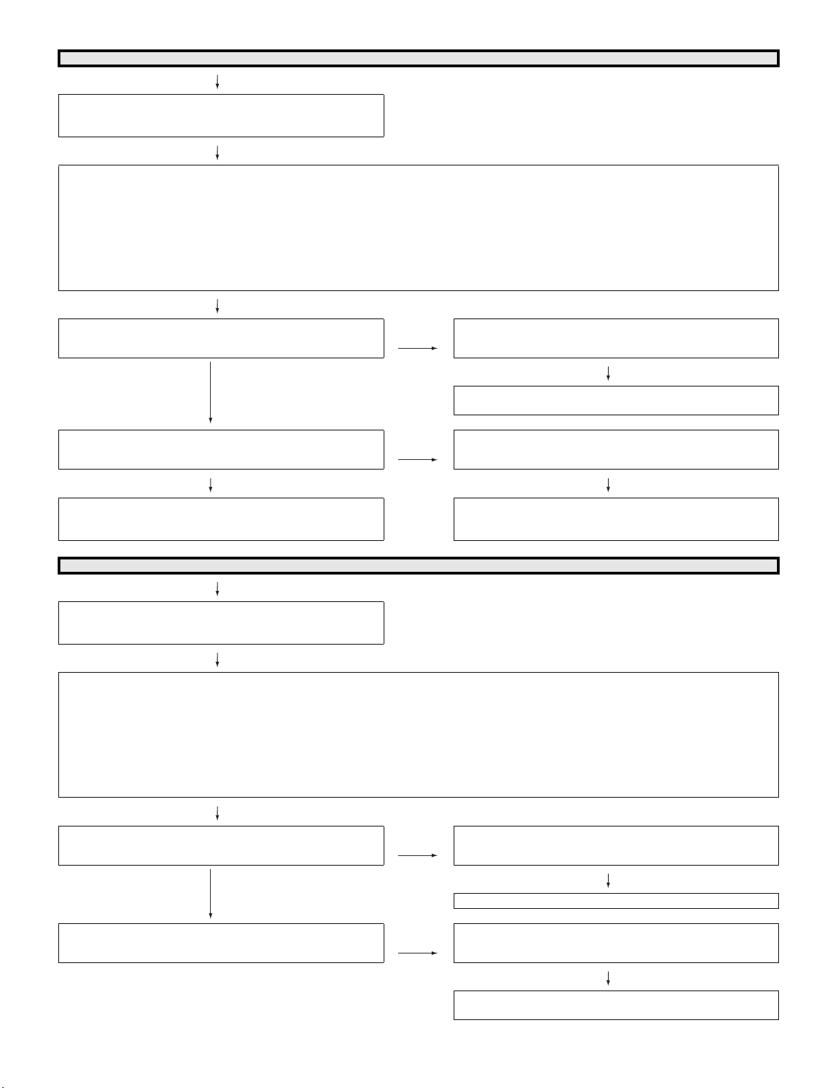
No sound (1-1) (during the reception of TV broadcasting)
No audio output during UHF/
VHF reception
Checklist:
1) Is the volume set to MIN or MUTE on the remote control? ••• Set the desired volume.
2) Is ANT-CABLE disconnected or connected improperly? ••• Connect it correctly as per the operation manual.
3) Attention: The terminal of IC3303 (VCT) cannot be actually checked by hiding oneself, and check it with another terminal of the same line,
please.
(MAIN-UNIT) (MAIN-UNIT)
Is the audio signal
(AOUT_SP_L/R) output from
pins (H26) and (H25) of
IC3303 (VCT)?
(MAIN-UNIT) YES
Is the audio signal
(SPKOUT_L/R) output form
pins (17) and (18) of
IC1302 (A-SW) normally?
NO Is the audio signal (SIF)
NO Check S9V power supply
(10) (15) pin, D3.3V
power supply (3) (36)
pin, and AUSW-MUTE
signal (29) pin of IC1302
(A-SW) or the peripheral
circuits.
input to pins (AB25) of
IC3303 (VCT)?
NO
Is the SIF signal output
from pin (4) of tuner
(TU1102)?
YES Check whether there are a
power supply of IC3303
(VCT), the short circuit,
and other abnormalities.
YES Check whether there are
open-circuit or short-circuit between tuner
(TU1102) and IC3303.
YES NO
Is the audio signal (LCH±/
RCH±) output form pins
(31)/(27) and (11)/(14) of
IC2701 (A-AMP) normally?
YES YES
Is the audio output signal
outputted to pins (1)-(4) of
SP-Connector (P2701) normally?
YES YES
Is the SP-Wire harness
connected and operated
orthopedically normally?
YES YES
Check right and left SPBOX, and exchange defec-
tive SP-BOX
(R: RSP-ZA392WJZZ/
L: RSP-ZA391WJZZ)
NO Check AMP12.5V power
supply (1) (10) pin, AMPSTBY input signal (17)
pin, and audio-mute signal pin (19) of IC2701 (AAMP) or the peripheral
circuits.
NO Check SP- Connector
(P2701) and peripheral
circuits.
NO Correct an abnormal part
of SP- harness.
A-BLOCK Replace tuner
Check whether IF5V
power supply is supplied to pin (3) of tuner
(TU1102), and ANT5V
power supply is supplied to pin (1) of tuner
(TU1102)?
Check whether the I2C
signal (SDA/SCL) is
functioning by (9) (8)
pin of tuner (TU1102).
Check whether IF_AGC
is functioning between
pins (E24) of IC3303
and pin (15) of tuner
(TU1102)
(TU1102).
NO Check whether there are
open-circuit or short-circuit between tuner
(TU1102) and Q1105 (5VREG) or between tuner
and IC1101.
NO Pursue an I2C line and
look for the part of an
open circuit or the Short
circuit.
NO Check whether there is an
open circuit or the short
circuit in an IF_AGC signal line.
4 – 5
Page 32

LC-32DH57E/RU/S (1st Edition)
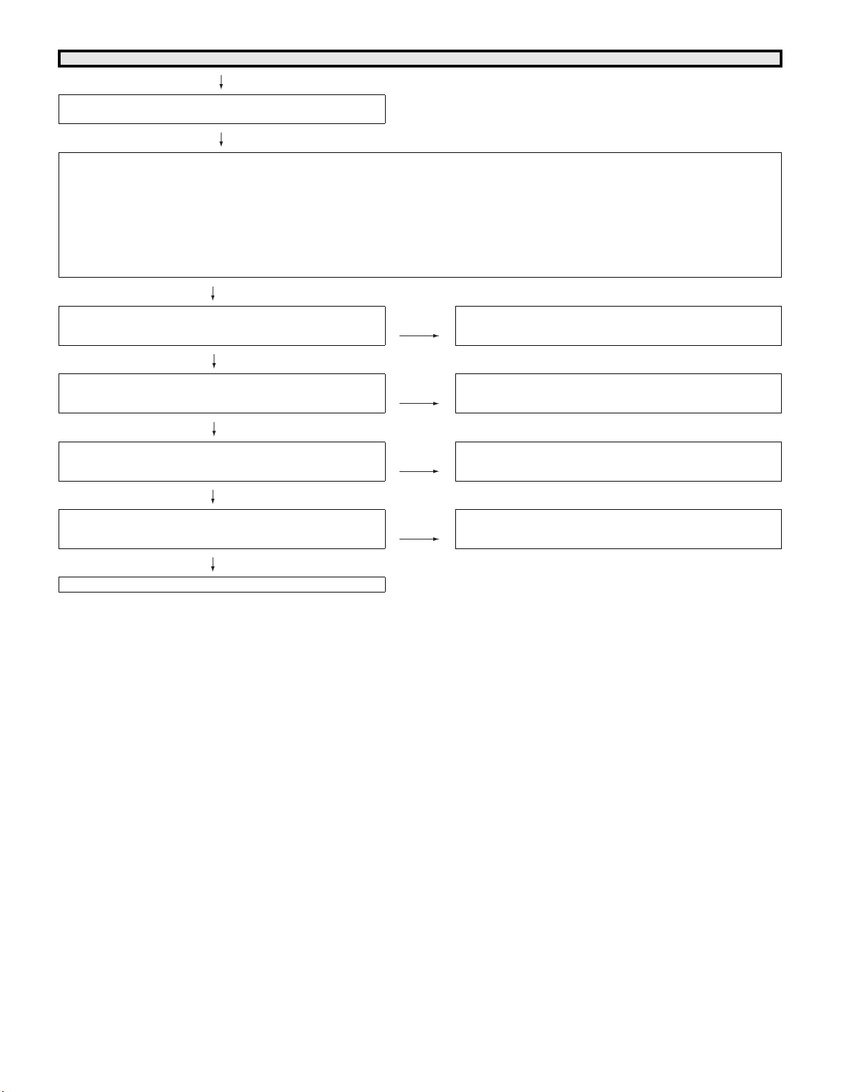
No sound (1-2) (during the reception of DTV broadcasting)
No audio output during DTV
reception
Checklist:
1) Is the volume set to MIN or MUTE on the remote control? ••• Set the desired volume.
2) Is ANT-CABLE disconnected or connected improperly? ••• Connect it correctly as per the operation manual.
3) Attention: The terminal of IC3303 (VCT) cannot be actually checked by hiding oneself, and check it with another terminal of the same line,
please.
(MAIN-UNIT) (MAIN-UNIT) (TUNER SIDE)
Is the audio signal
(AOUT_SP_L/R) output
from pins (H26) and (H25) of
IC3303 (VCT)?
NO Is the digital IF signal
(D_IF±) input to pins
(T25) (R25) of IC3303
(VCT)?
YES Check whether there
are a power supply of
IC3303 (VCT), the short
circuit, and other abnormalities.
(MAIN-UNIT) YES (OUTPUT_SIDE)
Is the audio signal
(SPKOUT_L/R) output
form pins (17) and (18) of
IC1302 (A-SW) normally?
YES NO
Is the audio signal (LCH±/
RCH±) output form pins
(31) (27) and (11) (14) of
IC2701 (A-AMP) properly?
YES YES
Is the audio output signal
outputted to pins (1)-(4) of
SP-Connector (P2701)
normally?
YES YES
Is the SP-Wire harness
(SP) connected and operated orthopedically normally?
NO Check S9V power supply
NO Check AMP12.5V power
NO Check SP-Connector
NO Correct an abnormal part
(10) (15) pin, D3.3V power
supply (3) (36) pin, and
AUSW-mute signal (29)
pin of IC1302 (A-SW) or
the peripheral circuits.
supply (1) (10) pin, AMPSTBY input signal (17) pin,
and audio-mute signal pin
(19) of IC2701 (A-AMP) or
the peripheral circuits.
(P2701) and peripheral circuits.
of SP- harness.
NO
Is the digital IF signal
(D_IF±) output from pins
(17) (16) of tuner
(TU1102)?
Check whether the IF5V
power supply is supplied to pin (3) of tuner
(TU1102).
Check whether the I2C
signal (SDA/SCL) is
functioning by pin (9) (8)
of tuner (TU1102).
Check whether IF_AGC
is functioning between
pins (E24) of IC3303
and pin (15) of tuner
(TU1102)
YES Check whether there
are open-circuit or
short-circuit between
tuner (TU1102) and
IC3303.
NO Check whether there
are open-circuit or
short-circuit between
Q1105 (5V-REG) and
tuner (TU1102).
NO Pursue an I2C line and
look for the part of an
open circuit or the Short
circuit.
NO Check whether there is
an open circuit or the
short circuit in an
IF_AGC signal line.
YES YES
Check right and left SPBOX, and exchange
defective SP-BOX
(R: RSP-ZA392WJZZ/
L: RSP-ZA391WJZZ)
A-BLOCK Replace tuner
(TU1102).
4 – 6
Page 33

No sound from external input devices (2-1)-1
No sound from EXT1 (SCART1) connecting an external input
device.
<EXT1>
Is the SC1_IN_L (SCART1-L-IN) audio signal input from pin (6)
of SCART1 terminal (SC503) to pin (44) of IC1302 (A-SW)?
Is the SC1_IN_R (SCART1-R-IN) audio signal input from pin (2)
of SCART1 terminal (SC503) to pin (43) of IC1302 (A-SW)?
YES
Is the audio signal (A_IN_L/R) properly output from pins (6) and
(7) of IC1302 (A-SW)?
YES
Is the audio signal (A_OUT_SP_L/R) properly output from pins
(H26) and (H24) of IC3303 (VCT)?
YES
It is the same as the above-mentioned A-BLOCK.
LC-32DH57E/RU/S (1st Edition)
NO Check pins (6) (2) of SCART1 and connection of an external
input device.
NO Check S9V power supply (10) (15) pin, D3.3V power supply (3)
(36) pin, and SDA0/SCL0 signal (28) (27) pin of IC1302 (A-SW)
or the peripheral circuit.
NO Check D3.3V power supply pin (F18) of IC3303 (VCT) and the
soldering confirmation or the peripheral circuit.
No sound from external input devices (2-1)-2
No sound from EXT2 (SCART2) connecting an external input
device.
<EXT2>
Is the SC2_IN_L (SCART2-L-IN) audio signal input from pin (6)
of SCART2 terminal (SC502) to pin (46) of IC1302 (A-SW)?
Is the SC2_IN_R (SCART2-R-IN) audio signal input from pin (2)
of SCART2 terminal (SC502) to pin (45) of IC1302 (A-SW)?
YES
Is the audio signal (A_IN_L/R) properly output from pins (6) and
(7) of IC1302 (A-SW)?
YES
Is the audio signal (A_OUT_SP_L/R) properly output from pins
(H26) and (H24) of IC3303 (VCT)?
YES
It is the same as the above-mentioned A-BLOCK.
NO Check pins (6) (2) of SCART2 and connection of an external
input device.
NO Check S9V power supply (10) (15) pin, D3.3V power supply (3)
(36) pin, and SDA0/SCL0 signal (28) (27) pin of IC1302 (A-SW)
or the peripheral circuit.
NO Check D3.3V power supply pin (F18) of IC3303 (VCT) and the
soldering confirmation or the peripheral circuit.
4 – 7
Page 34

LC-32DH57E/RU/S (1st Edition)
No sound from external input devices (2-2)-1
No sound from EXT3 (COMP-A-IN) connecting an external input
device.
<EXT3>
Is COMP_IN_L audio signal input to pin (2) of EXT3_AUDIO
(J502)?
Is COMP_IN_R audio signal input to pin (4) of EXT3_AUDIO
(J502)?
YES
Is COMP_IN_L audio signal input to pin (48) of IC1302 (A-SW)?
Is COMP_IN_R audio signal input to pin (47) of IC1302 (A-SW)?
YES
Is the audio signal (A_IN_L/R) properly output from pins (6) and
(7) of IC1302 (A-SW)?
YES
Is the audio signal (A_OUT_SP_L/R) properly output from pins
(H26) and (H25) of IC3303 (VCT)?
NO Check S9V power supply (10) (15) pin, D3.3V power supply (3)
(36) pin, and SDA0/SCL0 signal pin (28) (27) of IC1302 (A-SW)
or the peripheral circuit.
NO Check D3.3V power supply pin (F18) of IC3303 (VCT) and the
soldering confirmation or the peripheral circuit.
YES
It is the same as the above-mentioned A-BLOCK.
No sound from external input devices (2-2) -2
No sound from EXT4 (PC/HDMI-A-IN) connecting an external
input device.
<EXT4>
Is PC/HDMI-L audio signal input to pin (2) of EXT4 (J501)?
Is PC/HDMI-R audio signal input to pin (3) of EXT4 (J501)?
YES
Is PC/HDMI-L audio signal input to pin (50) of IC1302 (A-SW)?
Is PC/HDMI-R audio signal input to pin (49) of IC1302 (A-SW)?
YES
Is the audio signal (A_IN_L/R) properly output from pins (6) and
(7) of IC1302 (A-SW)?
YES
Is the audio signal (A_OUT_SP_L/R) properly output from pins
(H26) and (H25) of IC3303 (VCT)?
NO Check S9V power supply (10) (15) pin, D3.3V power supply (3)
(36) pin, and SDA0/SCL0 signal pin (28) (27) of IC1302 (A-SW)
or the peripheral circuit.
NO Check D3.3V power supply pin (F18) of IC3303 (VCT) and the
soldering confirmation or the peripheral circuit.
YES
It is the same as the above-mentioned A-BLOCK.
4 – 8
Page 35

No sound from external input devices (2-2)-3
No sound from EXT8 (CVBS-A-IN) connecting an external input
device.
<EXT8>
Is CVBS-L audio signal input to pin (5) of EXT8 (J505)?
Is CVBS-R audio signal input to pin (4) of EXT8 (J505)?
YES
Is CVBS-L audio signal input to pin (52) of IC1302 (A-SW)?
Is CVBS-R audio signal input to pin (51) of IC1302 (A-SW)?
YES
Is the audio signal (A_IN_L/R) properly output from pins (6) and
(7) of IC1302 (A-SW)?
YES
Is the audio signal (A_OUT_SP_L/R) properly output from pins
(H26) and (H25) of IC3303 (VCT)?
YES
It is the same as the above-mentioned A-BLOCK.
LC-32DH57E/RU/S (1st Edition)
NO Check S9V power supply (10) (15) pin, D3.3V power supply (3)
(36) pin, and SDA0/SCL0 signal pin (28) (27) of IC1302 (A-SW)
or the peripheral circuit.
NO Check D3.3V power supply pin (F18) of IC3303 (VCT) and the
soldering confirmation or the peripheral circuit.
No sound of external device (3-1)-1
No audio output from EXT1 (SCART1) terminal.
Checklist:
1) Is the MUTE button on the remote control set to ON? ••• Set to OFF.
2) Check the connection to external devices. •••Is there any improper connection?
Is audio signal output to pins (3) and (1) of EXT1 (SCART1)
(SC503)?
NO
Is the SC1-MUTE signal of base (5) (2) pin of Q502 “H”? YES The Q502 base should usually be “L”.
NO
Is the audio output signal (TUNER_OUT_L/R) output from pins
(11) and (10) of IC1301 (DAC) normal?
NO
Is the audio output signal (I2S_DATA_TU) output from pins (B25)
of IC3303 (VCT) normal?
YES Check EXT1 (SCART1) (SC503) and the connection to an exter-
nal device.
If it is “H” signal, Check whether base of Q1301 is “L” or peripheral circuit.
YES Check whether there are problems in IC1301 and Q502 or
peripheral circuits.
YES Check whether there is problem in IC3303.
NO
The input source of the audio is decided from TUNER. Is the SIF
signal input to pin (AB25) of IC3303 (VCT)?
NO
TUNER: TU1102
Check Q1101 (AMP), and pin (4) of TUNER.
YES Check whether there are problems in the power supply and sol-
dering IC3303 or peripheral circuits.
4 – 9
Page 36

LC-32DH57E/RU/S (1st Edition)
No sound of external device (3-1)-2
No audio output from EXT2 (SCART2) terminal.
Checklist:
1) Is the MUTE button on the remote control set to ON? •••• Set to OFF.
2) Check the connection to external devices. ••• Is there any improper connection?
Is audio signal output to pins (3) and (1) of EXT2 (SCART2)
(SC502)?
NO
Is the SC2-MUTE signal of base (5) (2) pin of Q501 “H”? NO The Q501 base should usually be “L”.
YES
Is the audio output signal (MONITOR_OUT_L/R) output from
pins (19) and (20) of IC1302 (A-SW) normally?
NO
Isn't there problem in the power supply input (S9V, D3.3V) of
IC1302 (A-SW), I2C_0 signal (SDA0/SCL0), and defective soldering, etc.?
YES Check EXT2 (SCART2) (SC502) and the connection to an exter-
nal device.
If it is “H” signal, Check whether base of Q1301 is “L” or peripheral circuit.
YES Check whether there are problems in IC1302, Q503, Q504 and
Q501 or peripheral circuits.
NO Repair the faulty point around IC1302.
YES
Where is the input source of the sound from?
(EXT1, EXT2, EXT3, EXT4, EXT8)
Check whether there is any problem in each input (terminal). EXT1/2: SCART1/2
Check pin (44) (43)/(46) (45) of IC1302 and pin (6) (2) of EXT1/2
terminal (SCART1/2).
EXT3: COMP
Check pin (48) (47) of IC1302, and pin (2) (4) of EXT3 terminal
(J502).
EXT4: PC/HDMI
Check pin (50) (49) of IC1302, and pin (2) (3) of EXT4 terminal
(J501).
EXT8: CVBS
Check pin (52) (51) of IC1302, and pin (5) (4) of EXT8 terminal
(J505).
4 – 10
Page 37

No sound of external device (3-2)
No sound from AUDIO OUT (J506). (MONITOR OUT)
Is the audio output signal send to pins (2) and (4) of the AUDIO
OUT terminal (J506)?
NO
Is the AUDIO-MUTE “L” signal input to pins (5) and (2) of Q509
base?
YES
Is the audio output signal (MONITOR_OUT_L/R) output from
pins (19) and (20) of IC1302 (A-SW) normally?
NO
Isn't there problem in the power supply input (S9V, D3.3V) of
IC1302 (A-SW), I2C_0 signal (SDA0/SCL0), and defective soldering, etc.?
YES
Where is the input source of the sound from?
(TUNER, EXT1, EXT1, EXT3, EXT4, EXT8)
LC-32DH57E/RU/S (1st Edition)
YES Check AUDIO OUT terminal (J506) and the connection to an
external device.
NO The Q1301 base should usually be “H”. If it is “L” signal, Check
pin (35) of IC1302, pin (1) of IC1303, and soldering.
YES Check the power supply input (S9V, D3.3V), soldering, and the
peripheral circuit of IC1302 (A-SW).
NO Repair the faulty point around IC1302.
Check whether there is any problem in each input (terminal). TU1102: TUNER
Check pin (AB25) of IC3303, and pin (4) of TUNER.
EXT1/2: SCART1/2
Check pin (44) (43)/(46) (45) of IC1302 and pin (6) (2) of EXT1/2
terminal (SCART1/2).
EXT3: COMP_L/R
Check pin (48) (47) of IC1302, and pin (2) (4) of EXT3 terminal
(J502).
EXT4: PC/HDMI_L/R
Check pin (50) (49) of IC1302, and pin (2) (4) of EXT4 terminal
(J501)
EXT8: CVBS_L/R
Check pin (52) (51) of IC1302, and pin (5) (4) of EXT8 terminal
(J505).
4 – 11
Page 38

LC-32DH57E/RU/S (1st Edition)
No sound of external device (3-3)
No DIGITAL sound from OPT OUT (D520).
Is the DIGITAL audio signal output to pin (1) of the OPT OUT terminal (D520)?
NO
Is the DIGITAL audio signal (OPT_ OUT) output from pin (4) of
IC503?
NO
Isn't the AUDIO_MUTE signal inputted into pin (1) of IC503 by
“L”?
NO
Is the DIGITAL audio signal (OPT_ OUT) output from pin (E26) of
IC3303 (VCT) normally?
NO
Isn't there problem in the power supply input (D3.3V, D1.1V) of
IC3303 (VCT), I2C_0 signal (SDA0/SCL0), and defective soldering, etc.?
YES Check OPT OUT terminal (D520) and the connection to an exter-
nal device.
YES Check whether it is normal between an OPT OUT terminal
(D520) and IC503.
YES The pin (1) of IC503 should usually be “H”. If it is “L” signal,
check Q505, pin (1) of Q1301 and pin (35) of IC1302.
YES Check whether it is normal between IC503 and IC3303.
NO Repair the faulty point around IC3303.
YES
Where is the input source of the sound from?
(TUNER, EXT5, EXT6, EXT7)
Check whether there is any problem in each input (terminal). TU1102: TUNER
Check pin (T25) (R25) of IC3303, and pin (16) (17) of TUNER.
EXT5: HDMI_1
Check the TMDS input signal of HDMI_1 (1) (9) pin, the TMDS I/
O signal of IC1508, and the TMDS input signal of IC3303.
EXT6: HDMI_2
Check the TMDS input signal of HDMI_2 (1) (9) pin, the TMDS I/
O signal of IC1508, and the TMDS input signal of IC3303.
EXT7: HDMI_3
Check the TMDS input signal of HDMI_3 (1) (9) pin, the TMDS I/
O signal of IC1508, and the TMDS input signal of IC3303.
4 – 12
Page 39

LC-32DH57E/RU/S (1st Edition)
<When tuner (U/V, DTV) is received> No picture on the display (1)-1
No picture appears on LCD during the tuner (U/V) reception.
Checklist:
1) Is “INPUT SOURCE” button on the remote control set up correctly? ••• set it as “TV” with the INPUT SOURCE button on the remote
control.
2) Is MENU-Picture-Backlight/Contrast/Brightness set to “MIN”? ••• Set it to an appropriate level.
3) Is ANT-CABLE disconnected or connected improperly? ••• Connect it correctly as per the operation manual.
4) Attention: The terminal of IC3303 (VCT) cannot be actually checked by hiding oneself, and check it with another terminal of the same line,
please.
YES
Is the level of pins (9) and (8) of tuner (TU1102) at “H”? NO These are communications lines for control (I2C). Follow the
path and check whether they are forced to L (PULL_DOWN).
(IC3303 (F25) (F24) pin)
YES
Is the video signal (VIDEO) output from pin (6) of tuner
(TU1102)?
YES
Is the video signal (TUNER_CVBS) input to pin (AD25) of lC3303
(VCT)?
NO Check the tuner (TU1102) and peripheral circuits.
NO Isn't there any part with short-circuits at IC3303 (VCT)? or Check
peripheral circuits.
YES
Is the LVDS video signal (LVDS0_D [0:4] ±) output from pin
[A6:A11], [B6:B11] of lC3303 (VCT)?
YES
Is the LVDS video signal (LVDS0_D [0:4] ±) input to pins (40)-
(28) of LW Connector (P2601), and is CLK signal (TCLK±) input
to pins (32)/(33)?
YES
Is the LCD12V input to (12)-(15) pin of LP Connector (P2604),
and is the I2C signal (VCOM_SDA/SCL) input to (3)/(4) pin?
YES
Exchange LCD-CONT-UNIT and do it operate normally?
NO
Check the contact of the LCD-CONT-UNIT connection harness
(CN3/4).
Exchange LCD-PANEL if it is useless even if it exchanges it.
NO Check IC3303 (VCT), and peripheral circuits.
NO Check whether there is short circuit between [A6:A11], [B6:B11]
pin of IC3303 (VCT) and (40)-(28) pin of LW Connector (P2601),
and peripheral circuits.
NO Check Q9606 (SW) for the LCD12V, and check IC2601 for the
I2C signal.
4 – 13
Page 40

LC-32DH57E/RU/S (1st Edition)
<When tuner (U/V, DTV) is received> No picture on the display (1)-2
No picture appears on LCD during the tuner (DTV) reception.
Checklist:
1) Is “INPUT SOURCE” button on the remote control set up correctly? ••• set it as “TV” with the INPUT SOURCE button on the remote
control.
2) Is MENU-Picture-Backlight/Contrast/Brightness set to “MIN”? ••• Set it to an appropriate level.
3) Is ANT-CABLE disconnected or connected improperly? ••• Connect it correctly as per the operation manual.
4) Attention: The terminal of IC3303 (VCT) cannot be actually checked by hiding oneself, and check it with another terminal of the same line,
please.
YES
Is the level of pins (9) and (8) of tuner (TU1102) at “H”? NO These are communications lines for control (I2C). Follow the
path and check whether they are forced to L(PULL_DOWN).
(IC3303 (F25) (F24) pin)
YES
Is the digital video signal (DIFP/N) output from pin (16) (17) of
tuner (TU1102)?
YES
Is the digital video signal (DIFP/N) input to pin (T25) (R25) of
lC3303 (VCT)?
NO Check the tuner (TU1102) and peripheral circuits.
NO Isn't there any part with short-circuits at IC3303 (VCT)? or Check
peripheral circuits.
YES
Is the LVDS video signal (LVDS0_D [0:4] ±) output from pin
[A6:A11], [B6:B11] of lC3303 (VCT)?
YES
Is the LVDS video signal (LVDS0_D [0:4] ±) input to pins (40)-
(28) of LW Connector (P2601), and is CLK signal (TCLK±) input
to pins (32)/(33)?
YES
Is the LCD12V input to (12)-(15) pin of LP Connector (P2604),
and is the I2C signal (VCOM_SDA/SCL) input to (3)/(4) pin?
YES
Exchange LCD-CONT-UNIT and do it operate normally?
NO
Check the contact of the LCD-CONT-UNIT connection harness
(CN3/4).
Exchange LCD-PANEL if it is useless even if it exchanges it.
NO Check IC3303 (VCT), and peripheral circuits.
NO Check whether there is short circuit between [A6:A11], [B6:B11]
pin of IC3303 (VCT) and (40)-(28) pin of LW Connector (P2601),
and peripheral circuits.
NO Check Q9606 (SW) for the LCD12V, and check IC2601 for the
I2C signal.
4 – 14
Page 41

LC-32DH57E/RU/S (1st Edition)
<When EXT1 is used for external input> No picture on the display (2)-1
No Composite video output when the EXT1 external input is
used.
Checklist:
1) Is “INPUT SOURCE” button on the remote control set up correctly? ••• set it as “EXT1” with the INPUT SOURCE button on the remote
control.
2) Is MENU-Picture-Backlight/Contrast/Brightness set to “MIN”? ••• Set it to an appropriate level.
3) Check the connection to the external device •••Connect it correctly as per the operation manual for the device.
4) Attention: The terminal of IC3303 (VCT) cannot be actually checked by hiding oneself, and check it with another terminal of the same line,
please.
Is the CVBS video signal (SC1_CVBS/Y) sent to pin (20) of
SCART1 (SC503)?
YES
Is the CVBS video signal (SC1_CVBS/Y) sent to input terminal
pin (AE24) of IC3303 (VCT)?
YES
Is the LVDS video signal (LVDS0_D [0:4]±) input to pins (40)-(28)
of LW Connector (P2601), and is CLK signal (TCLK±) input to
pins (32)/(33)?
NO Check external connection, input setting, SCART1 (SC503) and
peripheral circuits.
NO IC3303 (VCT), I2C_0signal (SDA0/SCL0), and peripheral cir-
cuits.
NO Check whether there is short circuit between [A6:A11], [B6:B11]
pin of IC3303 (VCT) and (40)-(28) pin of LW Connector (P2601),
and peripheral circuits.
YES
Is the LCD12V input to (12)-(15) pin of LP Connector (P2604),
and is the I2C signal (VCOM_SDA/SCL) input to (13)/(12) pin?
YES
Exchange LCD-CONT-UNIT and do it operate normally?
Check the contact of the LCD-CONT-UNIT connection harness
(CN3/4).
Exchange LCD-PANEL if it is useless even if it exchanges it.
NO Check Q9606 (SW) for the LCD12V, and check IC2601 for the
I2C signal.
4 – 15
Page 42

LC-32DH57E/RU/S (1st Edition)
<When EXT1 is used for external input> No picture on the display (2)-2
No RGB output when the EXT1 external input is used.
Checklist:
1) Is “INPUT SOURCE” button on the remote control set up correctly? ••• set it as “EXT1” with the INPUT SOURCE button on the remote
control.
2) Is MENU-Picture-Backlight/Contrast/Brightness set to “MIN”? ••• Set it to an appropriate level.
3) Check the connection to the external device •••Connect it correctly as per the operation manual for the device.
4) Attention: The terminal of IC3303 (VCT) cannot be actually checked by hiding oneself, and check it with another terminal of the same line,
please.
Is the RGB signal sent to pins (15), (11) and (7) of SCART1
(SC503)? (RED1, GREEN1, BLUE1)
NO Check external connection, input setting, SCART1 (SC503) and
peripheral circuits.
Is the RGB signal (RED1, GREEN1, BLUE1) sent to input terminal pins (AF24), (AD24) and (AD23) of IC3303 (VCT)?
YES
Is the LVDS video signal (LVDS0_D [0:4] ±) input to pins (40)-
(28) of LW Connector (P2601), and is CLK signal (TCLK±) input
to pins (32)/(33)?
YES
Is the LCD12V input to (12)-(15) pin of LP Connector (P2604),
and is the I2C signal (VCOM_SDA/SCL) input to (13)/(12) pin?
YES
Exchange LCD-CONT-UNIT and do it operate normally?
Check the contact of the LCD-CONT-UNIT connection harness
(CN3/4).
Exchange LCD-PANEL if it is useless even if it exchanges it.
NO Check between pins (15) (11) (7) of SCART1 (SC503) and pins
(AF24) (AD24) (AD23) of IC3303 (VCT) and peripheral circuits.
NO Check whether there is short circuit between [A6:A11], [B6:B11]
pin of IC3303 (VCT) and (40)-(28) pin of LW Connector (P2601),
and peripheral circuits.
NO Check Q9606 (SW) for the LCD12V, and check IC2601 for the
I2C signal.
4 – 16
Page 43

LC-32DH57E/RU/S (1st Edition)
<When EXT1 is used for external input> No picture on the display (2)-3
No Y/C output when the EXT1 external input is used.
Checklist:
1) Is “INPUT SOURCE” button on the remote control set up correctly? ••• set it as “EXT1” with the INPUT SOURCE button on the remote
control.
2) Is MENU-Picture-Backlight/Contrast/Brightness set to “MIN”? ••• Set it to an appropriate level.
3) Check the connection to the external device •••Connect it correctly as per the operation manual for the device.
4) Attention: The terminal of IC3303 (VCT) cannot be actually checked by hiding oneself, and check it with another terminal of the same line,
please.
Is the Y/C signal sent to pins (20) and (15) of SCART1 (SC503)?
(Y/C1)
YES
Is the Y/C signal (Y/C1) sent to input terminal pins (AE24) and
(AF24) of IC3303 (VCT)?
YES
Is the LVDS video signal (LVDS0_D [0:4] ±) input to pins (40)-
(28) of LW Connector (P2601), and is CLK signal (TCLK±) input
to pins (32)/(33)?
NO Check external connection, input setting, SCART1 (SC503) and
peripheral circuits.
NO Check between pins (20) (15) of SCART1 (SC503) and pins
(AE24) (AF24) of IC3303 (VCT), and peripheral circuits.
NO Check whether there is short circuit between [A6:A11], [B6:B11]
pin of IC3303 (VCT) and (40)-(28) pin of LW Connector (P2601),
and peripheral circuits.
YES
Is the LCD12V input to (12)-(15) pin of LP Connector (P2604),
and is the I2C signal (VCOM_SDA/SCL) input to (13)/(12) pin?
YES
Exchange LCD-CONT-UNIT and do it operate normally?
Check the contact of the LCD-CONT-UNIT connection harness
(CN3/4).
Exchange LCD-PANEL if it is useless even if it exchanges it.
NO Check Q9606 (SW) for the LCD12V, and check IC2601 for the
I2C signal.
4 – 17
Page 44

LC-32DH57E/RU/S (1st Edition)
<When EXT2 is used for external input> No picture on the display (3)-1
No composite video output when the EXT2 external input is
used.
Checklist:
1) Is “INPUT SOURCE” button on the remote control set up correctly? ••• set it as “EXT2” with the INPUT SOURCE button on the remote con-
trol.
2) Is MENU-Picture-Backlight/Contrast/Brightness set to “MIN”? ••• Set it to an appropriate level.
3) Check the connection to the external device ••• Connect it correctly as per the operation manual for the device.
4) Attention: The terminal of IC3303 (VCT) cannot be actually checked by hiding oneself, and check it with another terminal of the same line,
please.
Is the CVBS video signal sent to pin (20) of SCART2 (SC502)? NO Check external connection, input setting, SCART2 (SC502) and
peripheral circuits.
YES
Is the CVBS video signal (SC2_CVBS/Y) sent to input terminal
pin (AD26) of IC3303 (VCT)?
YES
Is the LVDS video signal (LVDS0_D [0:4] ±) input to pins (40)-
(28) of LW Connector (P2601), and is CLK signal (TCLK±) input
to pins (32)/(33)?
NO Check IC3303 (VCT), I2C_0 signal (SDA0/SCL0), and peripheral
circuits.
NO Check whether there is short circuit between [A6:A11], [B6:B11]
pin of IC3303 (VCT) and (40)-(28) pin of LW Connector (P2601),
and peripheral circuits.
YES
Is the LCD12V input to (12)-(15) pin of LP Connector (P2604),
and is the I2C signal (VCOM_SDA/SCL) input to (13)/(12) pin?
YES
Exchange LCD-CONT-UNIT and do it operate normally?
Check the contact of the LCD-CONT-UNIT connection harness
(CN3/4).
Exchange LCD-PANEL if it is useless even if it exchanges it.
NO Check Q9606 (SW) for the LCD12V, and check IC2601 for the
I2C signal.
4 – 18
Page 45

LC-32DH57E/RU/S (1st Edition)
<When EXT2 is used for external input> No picture on the display (3)-2
No Y/C output when the EXT2 external input is used.
Checklist:
1) Is “INPUT SOURCE” button on the remote control set up correctly? ••• set it as “EXT2” with the INPUT SOURCE button on the remote con-
trol.
2) Is MENU-Picture-Backlight/Contrast/Brightness set to “MIN”? ••• Set it to an appropriate level.
3) Check the connection to the external device ••• Connect it correctly as per the operation manual for the device.
4) Attention: The terminal of IC3303 (VCT) cannot be actually checked by hiding oneself, and check it with another terminal of the same line,
please.
Is the Y/C signal sent to pins (20) and (15) of SCART2 (SC502)?
(SC2_Y/C2)
YES
Is the Y/C signal (SC2_Y/C2) sent to input terminal pins (AD26)
and (AF25) of IC3303 (VCT)?
YES
Is the LVDS video signal (LVDS0_D [0:4] ±) input to pins (40)-
(28) of LW Connector (P2601), and is CLK signal (TCLK±) input
to pins (32)/(33)?
NO Check external connection, input setting, SCART2 (SC502) and
peripheral circuits.
NO Check between pins (20) (15) of SCART2 (SC502) and pins
(AD26) (AF25) of IC3303 (VCT) and peripheral circuits.
NO Check whether there is short circuit between [A6:A11], [B6:B11]
pin of IC3303 (VCT) and (40)-(28) pin of LW Connector (P2601),
and peripheral circuits.
YES
Is the LCD12V input to (12)-(15) pin of LP Connector (P2604),
and is the I2C signal (VCOM_SDA/SCL) input to (13)/(12) pin?
YES
Exchange LCD-CONT-UNIT and do it operate normally?
Check the contact of the LCD-CONT-UNIT connection harness
(CN3/4).
Exchange LCD-PANEL if it is useless even if it exchanges it.
NO Check Q9606 (SW) for the LCD12V, and check IC2601 for the
I2C signal.
4 – 19
Page 46

LC-32DH57E/RU/S (1st Edition)
<When EXT3/4/8 is used for external input> No picture on the display (4)-1
No Component video output when the EXT3 external input is
used.
Checklist:
1) Is “INPUT SOURCE” button on the remote control set up correctly? ••• set it as “EXT3”/”EXT4”/”EXT8” with the INPUT SOURCE button on
the remote control.
2) Is MENU-Picture-Backlight/Contrast/Brightness set to “MIN”? ••• Set it to an appropriate level.
3) Check the connection to the external device ••• Connect it correctly as per the operation manual for the device.
4) Attention: The terminal of IC3303 (VCT) cannot be actually checked by hiding oneself, and check it with another terminal of the same line,
please.
Is the component video signal sent to pin (3) (5) (7) of EXT3 terminal (J503)? (Y, Pb, Pr)
YES
Is the component video signal (COMP_Y/Pb/Pr) sent to input terminal pin (AE21) (AD22) (AF22) of IC3303 (VCT)?
YES
Is the LVDS video signal (LVDS0_D [0:4] ±) input to pins (40)-
(28) of LW Connector (P2601), and is CLK signal (TCLK±) input
to pins (32)/(33)?
NO Check external connection, input setting, EXT3 terminal (J503)
and peripheral circuits.
NO Check between pins (3) (5) (7) of EXT3 terminal (J503) and pins
(AE21) (AD22) (AF22) of IC3303 (VCT) and peripheral circuits.
NO Check whether there is short circuit between [A6:A11], [B6:B11]
pin of IC3303 (VCT) and (40)-(28) pin of LW Connector (P2601),
and peripheral circuits.
YES
Is the LCD12V input to (12)-(15) pin of LP Connector (P2604),
and is the I2C signal (VCOM_SDA/SCL) input to (13)/(12) pin?
YES
Exchange LCD-CONT-UNIT and do it operate normally?
Check the contact of the LCD-CONT-UNIT connection harness
(CN3/4).
Exchange LCD-PANEL if it is useless even if it exchanges it.
NO Check Q9606 (SW) for the LCD12V, and check IC2601 for the
I2C signal.
4 – 20
Page 47

LC-32DH57E/RU/S (1st Edition)
<When EXT3/4/8 is used for external input> No picture on the display (4)-2
No PC output when the EXT4 external input is used.
Checklist:
1) Is “INPUT SOURCE” button on the remote control set up correctly? ••• set it as “EXT3”/”EXT4”/”EXT8” with the INPUT SOURCE button on
the remote control.
2) Is MENU-Picture-Backlight/Contrast/Brightness set to “MIN”? ••• Set it to an appropriate level.
3) Check the connection to the external device ••• Connect it correctly as per the operation manual for the device.
4) Attention: The terminal of IC3303 (VCT) cannot be actually checked by hiding oneself, and check it with another terminal of the same line,
please.
Is the RGB signal sent to pins (1), (2) and (3) of EXT4 terminal
(PC_IN) (SC501)? (PC_R/G/B)
YES
Is the RGB signal (PC_R/G/B) sent to input terminal pins (AE20)
(AE19) and (AD19) of IC3303 (VCT)?
YES
Is the LVDS video signal (LVDS0_D [0:4] ±) input to pins (40)-
(28) of LW Connector (P2601), and is CLK signal (TCLK±) input
to pins (32)/(33)?
NO Check external connection, input setting, EXT4 terminal (PC_IN)
(SC501) and peripheral circuits.
NO Check between pins (1) (2) (3) of EXT4 terminal (PC_IN)
(SC501) and pins (AE20) (AE19) (AD19) of IC3303 (VCT).
NO Check whether there is short circuit between [A6:A11], [B6:B11]
pin of IC3303 (VCT) and (40)-(28) pin of LW Connector (P2601),
and peripheral circuits.
YES
Is the LCD12V input to (12)-(15) pin of LP Connector (P2604),
and is the I2C signal (VCOM_SDA/SCL) input to (13)/(12) pin?
YES
Exchange LCD-CONT-UNIT and do it operate normally?
Check the contact of the LCD-CONT-UNIT connection harness
(CN3/4).
Exchange LCD-PANEL if it is useless even if it exchanges it.
NO Check Q9606 (SW) for the LCD12V, and check IC2601 for the
I2C signal.
4 – 21
Page 48

LC-32DH57E/RU/S (1st Edition)
<When EXT3/4/8 is used for external input> No picture on the display (4)-3
No Composite video output when the EXT8 external input is
used.
Checklist:
1) Is “INPUT SOURCE” button on the remote control set up correctly? ••• set it as “EXT3”/”EXT4”/”EXT8” with the INPUT SOURCE button on
the remote control.
2) Is MENU-Picture-Backlight/Contrast/Brightness set to “MIN”? ••• Set it to an appropriate level.
3) Check the connection to the external device ••• Connect it correctly as per the operation manual for the device.
4) Attention: The terminal of IC3303 (VCT) cannot be actually checked by hiding oneself, and check it with another terminal of the same line,
please.
Is the Composite video signal sent to pin (6) of EXT8 terminal
(J505)? (CVBS_IN)
YES
Is the Composite video signal (CVBS_IN) sent to input terminal
pin (AC24) of IC3303 (VCT)?
YES
Is the LVDS video signal (LVDS0_D [0:4] ±) input to pins (40)-
(28) of LW Connector (P2601), and is CLK signal (TCLK±) input
to pins (32)/(33)?
NO Check external connection, input setting, EXT8 terminal (J505)
and peripheral circuits.
NO Check between pin (6) of EXT8 terminal (J505) and pin (AC24)
of IC3303 (VCT) and peripheral circuits.
NO Check whether there is short circuit between [A6:A11], [B6:B11]
pin of IC3303 (VCT) and (40)-(28) pin of LW Connector (P2601),
and peripheral circuits.
YES
Is the LCD12V input to (12)-(15) pin of LP Connector (P2604),
and is the I2C signal (VCOM_SDA/SCL) input to (13)/(12) pin?
YES
Exchange LCD-CONT-UNIT and do it operate normally?
Check the contact of the LCD-CONT-UNIT connection harness
(CN3/4).
Exchange LCD-PANEL if it is useless even if it exchanges it.
NO Check Q9606 (SW) for the LCD12V, and check IC2601 for the
I2C signal.
4 – 22
Page 49

LC-32DH57E/RU/S (1st Edition)
<When EXT5/6/7(HDMI) is used for external input> No picture on the display (5)-1
No HDMI0 digital video output when the EXT5 external input is
used.
Checklist:
1) Is “INPUT SOURCE” button on the remote control set up correctly? ••• set it as “EXT5”/”EXT6”/”EXT7” with the INPUT SOURCE button on
the remote control.
2) Is MENU-Picture-Backlight/Contrast/Brightness set to “MIN”? ••• Set it to an appropriate level.
3) Check the connection to the external device ••• Connect it correctly as per the operation manual for the device.
4) Attention: The terminal of IC3303 (VCT) cannot be actually checked by hiding oneself, and check it with another terminal of the same line,
please.
Is the HDMI Digital video signal sent to pin (1)-(9) of EXT5 terminal (SC1501)? (HDMI0_D [0:2] _P/N)
YES
Is the HDMI Digital video signal sent to pin (21)-(26) of IC1508
(HDMI-receiver)? (HDMI0_D [0:2] _P/N)
YES
Is HDMI_SW_ Digital Video signal sent to pin (AF16) (AE16)-
(AF18) (AE18) of input terminal of IC3303 (VCT)?
(HDMI_SW_D [0:2] P/N)
NO Check external connection, input setting, EXT5 terminal
(SC1501) and peripheral circuits.
NO Check short circuit of EXT5 terminal (SC1501), and peripheral
circuits.
NO Check short circuit of IC1508 (HDMI_receiver), power source
and peripheral circuits.
YES
Is the LVDS video signal (LVDS0_D [0:4] ±) input to pins (40)-
(28) of LW Connector (P2601), and is CLK signal (TCLK±) input
to pins (32)/(33)?
YES
Is the LCD12V input to (12)-(15) pin of LP Connector (P2604),
and is the I2C signal (VCOM_SDA/SCL) input to (13)/(12) pin?
YES
Exchange LCD-CONT-UNIT and do it operate normally?
Check the contact of the LCD-CONT-UNIT connection harness
(CN3/4).
Exchange LCD-PANEL if it is useless even if it exchanges it.
NO Check whether there is short circuit between [A6:A11], [B6:B11]
pin of IC3303 (VCT) and (40)-(28) pin of LW Connector (P2601),
and peripheral circuits.
NO Check Q9606 (SW) for the LCD12V, and check IC2601 for the
I2C signal.
4 – 23
Page 50

LC-32DH57E/RU/S (1st Edition)
<When EXT5/6/7(HDMI) is used for external input> No picture on the display (5)-2
No HDMI1 digital video output when the EXT6 external input is
used.
Checklist:
1) Is “INPUT SOURCE” button on the remote control set up correctly? ••• set it as “EXT5”/”EXT6”/”EXT7” with the INPUT SOURCE button on
the remote control.
2) Is MENU-Picture-Backlight/Contrast/Brightness set to “MIN”? ••• Set it to an appropriate level.
3) Check the connection to the external device ••• Connect it correctly as per the operation manual for the device.
4) Attention: The terminal of IC3303 (VCT) cannot be actually checked by hiding oneself, and check it with another terminal of the same line,
please.
Is the HDMI Digital video signal sent to pin (1)-(9) of EXT6 terminal (SC1502)? (HDMI1_D [0:2] _P/N)
YES
Is the HDMI Digital video signal sent to pin (13)-(18) of IC1508
(HDMI-receiver)? (HDMI1_D [0:2] _P/N)
YES
Is HDMI_SW_ Digital Video signal sent to pin (AF16) (AE16)-
(AF18) (AE18) of input terminal of IC3303 (VCT)?
(HDMI_SW_D [0:2] P/N)
NO Check external connection, input setting, EXT6 terminal
(SC1502) and peripheral circuits.
NO Check short circuit of EXT6 terminal (SC1502), and peripheral
circuits.
NO Check short circuit of IC1508 (HDMI_receiver), power source
and peripheral circuits.
YES
Is the LVDS video signal (LVDS0_D [0:4] ±) input to pins (40)-
(28) of LW Connector (P2601), and is CLK signal (TCLK±) input
to pins (32)/(33)?
YES
Is the LCD12V input to (12)-(15) pin of LP Connector (P2604),
and is the I2C signal (VCOM_SDA/SCL) input to (13)/(12) pin?
YES
Exchange LCD-CONT-UNIT and do it operate normally?
Check the contact of the LCD-CONT-UNIT connection harness
(CN3/4).
Exchange LCD-PANEL if it is useless even if it exchanges it.
NO Check whether there is short circuit between [A6:A11], [B6:B11]
pin of IC3303 (VCT) and (40)-(28) pin of LW Connector (P2601),
and peripheral circuits.
NO Check Q9606 (SW) for the LCD12V, and check IC2601 for the
I2C signal.
4 – 24
Page 51

LC-32DH57E/RU/S (1st Edition)
<When EXT5/6/7 (HDMI) is used for external input> No picture on the display (5)-3
No HDMI2 digital video output when the EXT7 external input is
used.
Checklist:
1) Is “INPUT SOURCE” button on the remote control set up correctly? ••• set it as “EXT5”/”EXT6”/”EXT7” with the INPUT SOURCE button on
the remote control.
2) Is MENU-Picture-Backlight/Contrast/Brightness set to “MIN”? ••• Set it to an appropriate level.
3) Check the connection to the external device ••• Connect it correctly as per the operation manual for the device.
4) Attention: The terminal of IC3303 (VCT) cannot be actually checked by hiding oneself, and check it with another terminal of the same line,
please.
Is the HDMI Digital video signal sent to pin (1)-(9) of EXT7 terminal (SC1503)? (HDMI2_D [0:2] _P/N)
YES
Is the HDMI Digital video signal sent to pin (3)-(8) of IC1508
(HDMI-receiver)? (HDMI2_D [0:2] _P/N)
YES
Is HDMI_SW_ Digital Video signal sent to pin (AF16) (AE16)(AF18) (AE18) of input terminal of IC3303 (VCT)?
(HDMI_SW_D [0:2] P/N)
NO Check external connection, input setting, EXT7 terminal
(SC1503) and peripheral circuits.
NO Check short circuit of EXT7 terminal (SC1503), and peripheral
circuits.
NO Check short circuit of IC1508 (HDMI_receiver), power source
and peripheral circuits.
YES
Is the LVDS video signal (LVDS0_D [0:4] ±) input to pins (40)-
(28) of LW Connector (P2601), and is CLK signal (TCLK±) input
to pins (32)/(33)?
YES
Is the LCD12V input to (12)-(15) pin of LP Connector (P2604),
and is the I2C signal (VCOM_SDA/SCL) input to (13)/(12) pin?
YES
Exchange LCD-CONT-UNIT and do it operate normally?
Check the contact of the LCD-CONT-UNIT connection harness
(CN3/4).
Exchange LCD-PANEL if it is useless even if it exchanges it.
NO Check whether there is short circuit between [A6:A11], [B6:B11]
pin of IC3303 (VCT) and (40)-(28) pin of LW Connector (P2601),
and peripheral circuits.
NO Check Q9606 (SW) for the LCD12V, and check IC2601 for the
I2C signal.
4 – 25
Page 52

LC-32DH57E/RU/S (1st Edition)
<When an external monitor is connected> No picture on the external monitor (6)-1
No picture appears on external monitor during the tuner (U/V)
reception. (Tuner input, EXT1 output)
Checklist:
1) Are input terminal on back of TV and “INPUT SOURCE” button on the remote control set up correctly? ••• See the operation manual and
set “INPUT SOURCE “appropriately. set to EXT***.
2) Is SCART-CABLE disconnected or connected improperly? ••• Connect it correctly as per the operation manual.
Is the video signal outputted to pin (19) of SCART1 (SC503)? YES Check SCART1, external connection or input setting.
NO
Is the video signal (SC1-VOUT) outputted from pin (2) of IC504
(75Ω_driver)?
NO
Is video signal (CVBS_TU_OUT) input to pin (4) of IC507? YES Check IC507 and peripheral circuits.
YES Check SCART1 (SC503) and peripheral circuits.
NO
Is video signal (TUNER_CVBS) outputted from emitter of
Q1102?
NO
Is video signal (VIDEO) outputted from pin (6) of TUNER
(TU1102)?
NO
Check IF5V power supply pins (3), 12C-line pins (9) and (8) of
tuner (TU1102) and peripheral circuits.
YES Check IC3303 and peripheral circuits.
4 – 26
Page 53

LC-32DH57E/RU/S (1st Edition)
<When an external monitor is connected> No picture on the external monitor (6)-2
No picture appears on external monitor during the EXT8 input
(COMPOSITE).
(EXT8 COMP input, EXT2 output)
Checklist:
1) Are input terminal on back of TV and “INPUT SOURCE” button on the remote control set up correctly? ••• See the operation manual and
set “INPUT SOURCE” appropriately. set to EXT***.
2) Is SCART-CABLE disconnected or connected improperly? ••• Connect it correctly as per the operation manual.
Is the video signal outputted to pin (19) of SCART2 (SC502)? YES Check SCART2, external connection or input setting.
NO
Is the video signal (SC2-VOUT) outputted from pin (4) of IC508
(75Ω_driver)?
NO
Is the Composite Video signal (CVBS_MON_OUT) outputted
from the pin (B13) of IC3303 (VCT)?
YES Check IC508 and peripheral circuits.
YES Check between IC508 and IC3303 and the peripheral circuitry.
NO
Is the Composite signal (CVBS_IN) inputted to pins (6) of EXT8
terminal normally?
NO
Check whether the terminal of EXT8 is faulty, or there is not any
error in external connection.
YES Check a short circuit etc. between the EXT8 input terminal (pin
(6)) and IC3303 (VCT).
4 – 27
Page 54

LC-32DH57E/RU/S (1st Edition)
<When an external monitor is connected> No picture on the external monitor (6)-3
No picture appears on external monitor during the EXT5/6/7
inputs (HDMI). (EXT5 HDMI input, EXT2 output)
Checklist:
1) Are input terminal on back of TV and “INPUT SOURCE” button on the remote control set up correctly? ••• See the operation manual and
set “INPUT SOURCE” appropriately. set to EXT***.
2) Is SCART-CABLE disconnected or connected improperly? ••• Connect it correctly as per the operation manual.
Is the video signal outputted to pin (19) of SCART2 (SC502)? YES Check SCART2, external connection or input setting.
NO
Is the video signal (SC2-VOUT) outputted from pin (4) of IC508
(75Ω_driver)?
NO
Is the Composite Video signal (CVBS_MON_OUT) outputted
from the pin (B13) of IC3303 (VCT)?
YES Check IC508 and peripheral circuits.
YES Check between IC508 and IC3303 and the peripheral circuitry.
NO
Is the HDMI output signal (HDMI_SW_D [0:2] P/N) input to the
pin [AF16-AE18] of IC3303 (VCT) normally?
NO
Is the HDMI input signal (HDMI0/1/2_D [0:2] P/N) input to IC1508
(HDMI-receiver) normally?
NO
Are the pin (43) (44)/(39) (40)/(33) (34) of I2C signal (HDMI [0:2]
_SDA/SCL) accessed normally?
YES
Is the TMDS signal (1-12) pin inputted to HDMI1/2/3 (EXT5/6/7)
terminal normally?
NO
Check whether the terminal of HDMI1/2/3 (EXT5/6/7) is faulty, or
there is not any error in external connection.
YES Check a short circuit, HDMI_H/V signal, HDMI_PLG signal, and
other abnormality, etc. with IC3303.
YES Check a short circuit, HDMI_I2C signal, and other abnormality,
etc. with IC1508.
NO Exchange HDMI-Receiver (IC1508) Or check short circuit.
YES Check a short circuit etc. between HDMI1/2/3 and IC1508
(HDMI-receiver).
4 – 28
Page 55

LC-32DH57E/RU/S (1st Edition)
The backlight does not light up.
Do all the fluorescent tubes light up? YES Check each fluorescent tube and exchange defective fluorescent
tubes.
NO
Is 60V supplied to Connector (CN7302) (20-23) pin? NO Refer to troubleshooting “No power supply (Front LED does not
YES
Is UR12.5V supplied to Connector (CN7302) (10)pin? NO Refer to troubleshooting “No power supply” (Front LED does not
YES
Is UR12.5V supplied to (26) pin of IC7700 (INV-CTL)? NO Check UR12.5V-line in an INVERTER unit.
YES
Is the STB-ON/OFF signal supplied to (16) pin (or (4) pin of a
connector (CN7302)) of IC7700 (INV-CTL)?
YES
Is each control signal coming to the connector in INV-UNIT
(CN7302)?
• ADIM (Tube current setting): (1pin)
• OFL (PWM light control signal input): (2pin)
• ERR (Lamp error output): (3pin)
• BRT (Light control method identificatio): (5pin)
NO Check the STB-ON/OFF signal-line in an INVERTER unit.
NO Check each control circuit.
light up)” of a power supply.
Or check a peripheral circuit. (Q7809, Q7807, Q7811, Q7810)
light up) of a power supply. Or check a peripheral circuit.
ADIM-H: Tube current 12mA, L: Tube current 8.5mA
OFL -H: Lamp ON, L: Lamp OFF
ERR -H: Normal, L: Error
REG2-H: External PWM input, L: Analog voltage input
YES
Is [0] displayed as the number of [LAMP_ERROR] in the process
mode?
YES
Is the drive output signal sent from PIN (31) and (32) of IC7700
(INV-CTL)?
YES
Does the drive output circuit normally work?
(Q7800-Q7806)
(Q7809, Q7807, Q7811, Q7810)
YES
Is the circuit by the side of secondary operating normally?
(T7903-T7905)
YES
Is the circuit by the side of secondary operating normally?
(D7900-D7905)
(D7919/D7921/D7923/D7925/D7927/D7929)
NO Reset the number of [LAMP_ERROR] to the default value in the
process mode.
NO Check IC7700 (INV-CTL) and the peripheral circuits.
NO Check which parts are defective.
And exchange the non-conforming articles.
NO Check defective parts and exchange the inferior products.
NO Check defective parts and exchange the inferior products.
4 – 29
Page 56

LC-32DH57E/RU/S (1st Edition)
LCD failure (1)
Does a single or several
vertical stripes appear
on the LCD screen?
The backlight functions. Does not the
image come out in the
LCD screen
(screen black)?
Does a single or several
horizontal stripes appear
on the LCD screen?
Does the entire LCD
screen look whitish all
over?
Do luminescent or black
dots appear on the
screen?
Replace the LCD panel.
LCD failure (2)
Does the QS drive function?
Replace the LCD_CONT_UNIT.
Is the on-screen image
rippling or distorted?
Are the data bit dropout?
(No solution even when
turning on and off the QS
drive)
Is there any portion
which some screens
were darkish or
became whitish?
Is the gamma correction as specified?
4 – 30
Page 57

LC-32DH57E-BK
CHAPTER 5. MAJOR IC INFOMATIONS
[1] MAJOR IC INFOMATIONS
1. DESCRIPTION OF MAJOR ICs
LC-32DH57E/RU/S (1st Edition)
Service Manual
Ref No. Name Part Code Description
[MAIN UNIT]
IC1301 VHiAK4341ED-1Y DAC AK4341 is 24 bits DAC of 2Vrms output. A newly developed advanced
multiple bit system is adopted in the modulator. In this model, this
IC is used to use the audio signal from a digital tuner as an audio output signal of SCART1.
IC1302 VHiMT8292N+-1Q Audio multiplexer The MediaTek MT8292 introduces the advantages of an input multi-
plexer, the headphone driver and the PGA outputs. The analog input
pins can either independently support GPIO function or provide extra
GPIO pins to use. The analog input pins can either independently support GPIO function or provide extra GPIO pins to use.
IC1303 VHiS80944NM-1Y Voltage detector with built-
in delay circuit
IC501 VHi2BR24C21F-1Y
for service
(RH-iXC206WJQZS)
IC506 VHiM3221EiP-1Y RS232C-DRIVER The MAX3221E is a single driver, single receiver RS-232 solution
IC1508 VHiSii91873-1Q HDMI_Port _Processor The SiI91873 HDMI port processor is the second generation of HDMI
IC3302 VHiBD6538G+-1Y USB high side SW BD6538G is single channel high side powers switch with low ON resis-
IC3303 RH-iXC758WJQZQ VCT & Main CPU This IC is Video Processor & MAIN CPU.
IC3304 VHiS80928NM-1Y Voltage detector with built-
IC3305 VHiS80920NM-1Y Voltage detector with built-
IC3501/2 RH-iXC505WJQZQ 512Mb-DDR2-SDRAM This IC is 512Mb DDR2 SDRAM.
IC8403 RH-iXC788WJN2Y 2Mb-FLASH This IC is 2Mbit CMOS 3.0 Volt Flash Memory with 50-MHz SPI
IC8401 RH-iXC721WJQZQ 512Mb-NAND-FLASH This IC is 512Mb NAND flash memory.
IC8455 VHiBR24S64F-1Y I2C bus type-64K
1K E2PROM This IC is a 1Kbit-2-wire (I2C bus type) serial EEPROM that can be
in delay circuit
in delay circuit
E2PROM
This IC is a highly precision voltage detector (4.4V) with built-in delay
circuit.
In this model, It used as voltage detector of MUTE signal.
programmed electrically. The EEPROM chip stores the EDID data of
PC input. This data is controlled through I2C signals.
operating from a single Vcc supply. The RS-232 pins provide IEC
G1000-4-2 ESD Protection. The device meets the requirements of
TIA/EIA-232-F and provides the electrical interface between an asynchronous communication controller and the serial-port connector.
The charge pump and four small external capacitors allow operation
from a single 3V to 5.5V supply.
devices that support revision 1.3 of the HDMI specification.
The main feature is as follows.
1) 4-input, 1-output HDMI port processor.
2) Integrated TMDS receiver and transmitter cores capable of receiving and transmitting at 2.25Gbps.
3) Supports video resolutions up to 1080p, 60Hz, 12bit or 720p/1080i,
120Hz,12bit.
4) Receiver fully comply with DVI1.0, HDCP1.1 and HDMI1.3 specifications.
tance Nch power MOSFET.
Rich safety functions such as over current detection, Thermal shutdown (TSD), under voltage lock out (UVLO) and soft start function
which are required for the power supply port protection are integrated
into 1chip.
In this IC, the decode processing and the video signal processing are
done.
Moreover, OSD is generated here and added to a picture signal.
This IC is a highly precision voltage detector (2.8V) with built-in delay
circuit. In this model, It uses as RESET signal of IC3303.
This IC is a highly precision voltage detector (2.0V) with built-in delay
circuit. In this model, It used as a D-POW signal generator.
This IC operates as a memory of IC3303 (Video Processor). ***
(Serial Peripheral Interface) Bus and Small Sector for Boot and
Parameter Storage.
This IC stores the software data that processes the system of TV such
as the graphic processing, the LCD controls, and backlights etc.
The BR24S64F is a 64Kbit-2-wire (I2C bus type) serial EEPROM that
can be programmed electrically.
This IC stores the menu data and the adjustment value data of adjustment process mode etc.
The data is given out by commands from the main microprocessor.
Drawing
No.
1/10
1/10
1/10
2/10
2/10
3/10
4/10
4/10
4/10
4/10
5/10
6/10
6/10
6/10
5 – 1
Page 58

LC-32DH57E/RU/S (1st Edition)
Ref No. Name Part Code Description
IC4402 VHiAOZ1320C-1Y SMART LOAD SW The AOZ1320 is a P-channel high-side load switch with controlled
slew rate. AOZ1320-04 have a slew rate of 1ms.
IC4401 VHiMT8295AE-1Q IC Controller This is a control IC for PCMCIA cards. This controls information on IC
cards inserted into the PCMCIA card slot (SC4401) or information on
software version upgrade cards saved on flash memories to transfer
the data to CPUs and memories.
IC2701 VHiYDA148QZ-1Y A-AMP This IC is a digital audio power amplifier. It is mounted by 32QFN
IC9605 VHiLV5893M+-1Y 1CH-SW-REG
BU3.3V-REG
IC9608 VHiLV5893M+-1Y 1CH-SW-REG
D5V-REG
IC9606 VHiLV5805M+-1Y 1CH-SW-REG
IC9611 VHiTCR5SB25-1Y 1CH-SW-REG
IC9604 VHiLV58072M-1Y 1CH-SW-REG
IC9607 VHiS80944NM-1Y Voltage detector with built-
IC2601
IC9601
[POWER UNIT]
IC7201 VHiSTRY64761E SWING-P-CTL This product is hybrid IC for the pseudoresonant switching power sup-
IC7101 VHiNCP1606B-1Y Power Factor Controller The NCP1606 is an active power factor controller specifically
[INVERTER UNIT]
IC7700 VHiBD9897FS-1Y DC/AC-CONVERTER BD9897FS is IC for DC-AC inverter control. Functions of soft start cir-
VHiHC2G66DP-1Y Bilateral Switch This IC is provides a dual analog switch. Each switch has two pins for
D1.8V-REG
2.5V-REG
D1.1V-REG
in delay circuit
small package with 15W or less stereo. it drives by 10W in 26, and 32
types.
LV5893M is 1.8A 1ch step down switching regulator.
In this model, it generate BU3.3V.
LV5893M is 1.8A 1ch step down switching regulator.
In this model, it generate D5V.
LV5805M is 2A 1ch step down switching regulator.
In this model, it generate D1.8V.
The TCR5SB25 is CMOS general-purpose single-output voltage regulators with an on/off control input, featuring low dropout voltage and
low quiescent bias current. The output current is possible up to 200mA
or less. In this model, it generate CPU2.5V.
LV58072M is 3A 1ch step down switching regulator.
In this model, it generate D1.1V.
This IC is a highly precision voltage detector with built-in delay circuit.
In this model, It used as enable signal of BU3.3V_REG.
input or output and an active HIGH enable input.
ply with built-in power MOSFET and multifunctional control IC. Highly
effective and the low noise are achieved by a pseudoresonance and
the bottoms ticket operation at the normal operation, and low power
consumption is achieved at the standby by the thing that intermittent
oscillates.
designed for use as a pre-converter in electronic ballasts, ac-dc adapters and other medium power off line converters.
cuit, timer latch circuit, and under voltage lock output circuit (UVLO),
etc. are built into this IC.
Drawing
No.
7/10
7/10
9/10
10/10
10/10
10/10
10/10
10/10
10/10
8/10
10/10
5 – 2
Page 59

2. Detailed ICs Information
2.1. IC1301 (VHiAK4341ED-1Y)
2.1.1 Block Diagram
LC-32DH57E/RU/S (1st Edition)
2.1.2 Pin Connections and short description
Pin No. Pin Name I/O Pin Function
1 MCLK I Master clock input pin. An external TTL clock should be input on this pin.
2 BICK I Audio serial data clock pin.
3 SDTI I Audio serial data input pin.
4 LRCK I L/R clock pin.
5 RDN I Power-down mode pin.
6 SMUTE I Soft mute pin in parallel control mode.
7 ACKS I Auto setting mode pin.
8 DIF I Audio data interface format pin.
9 DEM I De-emphasis enable pin.
10 AOUTR O Rch analog output pin.
11 AOUTL O Lch analog output pin.
12 HVDD I Output buffer power supply pin.
13 VSS — Ground pin.
14 VDD — DAC power supply pin.
15 VCOM O DAC common voltage pin.
16 GAIN I Gain control pin.
When at “L”, the AK4341 is in the power-down mode, held in reset and AOUTL/R are held in VCOM.
The AK4341 must be reset once upon power-up.
“H”: Enable, “L”: Disable
“L”: Manual setting mode, “H”: Auto setting mode.
“L”: 24bit MSB justified, “H”; I2S.
“H”: Enable, “L”: Disable
When PDN pin = “L”, outputs VCOM voltage.
When PDN pin = “L”, outputs VCOM voltage.
Normally connected to VSS with a 0.1µF ceramic capacitor in parallel with a 10µF electrolytic cap.
Normally connected to VSS with a 10µF electrolytic cap.
Outputs VCOM VDD voltage either PDN pin = “L” or “H”.
“H”: +6dB, “L”: 0dB, open: +12dB.
When PDN = “H”, the gain pin is connected to VDD and VSS with 50kΩ resister and held to VDD/2 when open.
When PDN = “L”, connected to VSS with 50kΩ resister.
5 – 3
Page 60

LC-32DH57E/RU/S (1st Edition)
2.2. IC1302 (VHiMT8292N+-1Y)
2.2.1 Block Diagram
5 – 4
Page 61

LC-32DH57E/RU/S (1st Edition)
2.2.2 Pin Connections and short description
Pin No. Pin Name I/O Pin Function sheet name
1 AIN8R I Channel 8 right input. open
2 AIN8L I Channel 8 left input. open
3 MVDD33 — Multiplexer positive supply 3.3 voltage. —
4 VCM33 O Multiplexer midrail divider decoupling pin. C-GND
5 MGND33 — Multiplexer negative supply. GND
6 ADCOUTL O Analog multiplexer left output. AUDIO_IN_L
7 ADCOUTR O Analog multiplexer right output. AUDIO_IN_R
8 HPOUTL O Headphone right channel output. HP_L
9 HPGND — Headphone ground supply pin. GND
10 HPVDD — Headphone power supply pin. S9V
11 HPOUTR O Headphone right channel output. HP_R
12 AGND — Analog negative supply. GND
13 PGA0OUTL O PGA channel 0 left output. open
14 PGA0OUTR O PGA channel 0 right output. open
15 AVDD — Analog positive supply 12 voltage or 9 voltage. S9V
16 VCMPGA O PGA midrail divider decoupling pin. C-GND
17 PGA2OUTL O PGA channel 2 left output. SPK_OUT_L
18 PGA2OUTR O PGA channel 2 right output. SPK_OUT_R
19 PGA1OUTL O PGA channel 1 left output. MONITOR_L
20 PGA1OUTR O PGA channel 1 right output. MONITOR_R
21 INPUT2R I Channel 2 right input to PGA gain module. AOUT_SP_R
22 INPUT2L I Channel 2 left input to PGA gain module. AOUT_SP_L
23 INPUT0R I Channel 0 right input to PGA gain module. AOUT_HP_R
24 INPUT0L I Channel 0 left input to PGA gain module. AOUT_HP_L
25 INPUT1R I Channel 1 right input to PGA gain module. AOUT_MONI_R
26 INPUT1L I Channel 1 left input to PGA gain module. AOUT_MONI_L
27 CL I Control clock pin in serial mode. SCLO_400K
28 DI I/O Control data pin in serial mode. SDAO_400K
29 MUTE# I Hardware mute function when this pin is driven low. AUSW_MUTE
30 RESET# I The device enters a low power mode when this pin is driven low. AUSW_RST
31 GPIO0 I General Purpose I/O 0 and also shares hardware trapped function. R-GND
32 GPIO1 I General Purpose I/O 1. open
33 GPIO2 I General Purpose I/O 2. open
34 GPIO3 I General Purpose I/O 3. COMP_PLUG
35 GPIO4 I General Purpose I/O 4. MUTE_A_ALL
36 DVDD — Digital positive supply 3.3 voltage. D3.3V
37 DGND — Digital negative supply. ground
38 GPIO5 I General Purpose I/O 5. open
39 GPIO6 I General Purpose I/O 6. open
40 GPIO7 I General Purpose I/O 7. TUNER_OUT_SEL
41 GPIO8 I General Purpose I/O 8. TUNER_OUT_CVBS_MUTE
42 GPI I Only General Purpose Input and support internal digital scan mode. CVBS_PLUG
43 AIN1R I Channel 1 right input (default). SC1_IN_R
44 AIN1L I Channel 1 left input (default). SC1_IN_L
45 AIN2R I Channel 2 right input. SC2_IN_R
46 AIN2L I Channel 2 left input. SC2_IN_L
47 AIN3R I Channel 3 right input. COMP_IN_R
48 AIN3L I Channel 3 left input. COMP_IN_L
49 AIN4R I Channel 4 right input. RC/HDMI_IN_R
50 AIN4L I Channel 4 left input. RC/HDMI_IN_L
51 AIN5R I Channel 5 right input. CVBS_IN_R
52 AIN5L I Channel 5 left input. CVBS_IN_L
53 AIN6R I Channel 6 right input. open
54 AIN6L I Channel 6 left input. open
55 AIN7R I Channel 7 right input. open
56 AIN7L I Channel 7 left input. open
5 – 5
Page 62

LC-32DH57E/RU/S (1st Edition)
2.3. IC1303, IC9607 (VHiS80944NM-1Y)
2.3.1 Block Diagram
2.3.2 Pin Connections and short description
Pin No. Pin Name I/O Pin Function
1 OUT O Voltage detection output terminal (RESET detecting voltage).
2 VDD — Voltage input terminal.
3 VSS — Ground terminal.
4 NC — No connection (It is an opening electrically.)
5 CD I External capacitor connection terminal for delay.
5 – 6
Page 63

2.4. IC506 (VHiM3221EiP-1Y)
This IC is a block diagram and description LC-19D1E (S58J9LC19D1ES) please see the service manual.
2.5. IC1508 (VHiSii91873-1Q)
2.5.1 Block Diagram
LC-32DH57E/RU/S (1st Edition)
5 – 7
Page 64

LC-32DH57E/RU/S (1st Edition)
2.5.2 Pin Connections and short description
Pin No. Pin Name I/O Pin Function
HDMI RX Port Pins
68 R0X0P I TMDS input port 0 data pairs.
67 R0X0N I
70 R0X1P I
69 R0X1N I
72 R0X2P I
71 R0X2N I
66 R0XCP I TMDS input port 0 clock pair.
65 R0XCN I
4 R1X0P I TMDS input port 1 data pairs.
3 R1X0N I
6 R1X1P I
5 R1X1N I
8 R1X2P I
7 R1X2N I
2 R1XCP I TMDS input port 1 clock pair
1R1XCN I
14 R2X0P I TMDS input port 2 data pairs.
13 R2X0N I
16 R2X1P I
15 R2X1N I
18 R2X2P I
17 R2X2N I
12 R2XCP I TMDS input port 2 clock pair.
11 R2XC N I
22 R3X0P I TMDS input port 3 data pairs.
21 R3X0N I
24 R3X1P I
23 R3X1N I
26 R3X2P I
25 R3X2N I
20 R3XCP I TMDS input port 3 clock pair
19 R3XCN I
HDMI Tx Port Pins
60 TX0P O HDMI Tx Output port data.
61 TX0N O TMDS Low Voltage Differential Signal output data pairs.
58 TX1P O
59 TX1N O
56 TX2P O
57 TX2N O
62 TXCP O
63 TXCN O
System Switching Pins
29 DSDA0 I/O DDC I2C Data for respective port. These signals are true open drain, and do not pull-down to ground when
33 DSDA1 I/O
39 DSDA2 I/O
43 DSDA3 I/O
30 DSCL0 I DDC I2C Clock for respective port. These signals are true open drain, and do not pull-down to ground when
34 DSCL1 I
40 DSCL2 I
44 DSCL3 I
32 R0PWR5V — 5-V Port detection input for respective port. Connect to 5-V signal from HDMI input connector.
36 R1PWR5V —
42 R2PWR5V —
46 R3PWR5V —
31 HPD0 O Hot Plug Detect Output for respective port. Connect to HOTPLUG of HDMI input connector.
35 HPD1 O
41 HPD2 O
45 HPD3 O
49 R4PWR5V — 5V power from 5th Rx port.
power is not applied to the device. These pins require an external pull-up resistor.
power is not applied to the device. These pins require an external pull-up resistor.
5 – 8
Page 65

LC-32DH57E/RU/S (1st Edition)
Pin No. Pin Name I/O Pin Function
Control Pins
54 CSCL I Local Configuration/Status I2C Clock. Chip configuration/status is accessed via this I2C port.
This pin is a true open drain, so it does not pull to ground if power is not applied.
53 CSDA I/O Local Configuration/Status I2C Data. Chip configration/status is accessed via this I2C port.
This pin is a true open drain, so it does not pull to ground if power is not applied.
48 DSCL4 I DDC I2C Clock for VGA port. HDCP KSV, Aa, and Ri values are exchanged over this I2C port during authen-
tication. This pin is a true open drain, so it does not pull to ground if power is not applied.
The R4PWR5V (VREF) pad will provide a reference voltage for the PROT input pin.
47 DSDA4 I/O DDC I2C Data for VGA port. HDCP KSV, Aa, and Ri values are exchanged over this I2C port during authen-
Configuration Pins
55 TPWR_CI2CA I/O I2C Slave Address input/Transmit Power Sense Output. When RESET# is LOW, this pin is used as an input
52 INT O Interrupt Output.
10 RSVD — When SBVCC (pin38) = 5V, RSVD pin #10 must be tied to GND with less than 10K resistor.
28 RSVD — These pins must be tied to GND during normal operation.
CEC Pins
50 CEC_A I/O HDMI compliant CEC I/O used for interfacing to CEC devices. The signal is electrically compliant with CEC
51 CEC_D I/O This pin is configurable through NVRAM. For CEC_D use, this pin interfaces to the CEC master. Usually
Power and Ground Pins
9,27,64 VCC33 — TMDS Core VCC. Must be supplied at 3.3V
37 MICOM_VCC33 — During normal mode, this pin provides 3.3V power to external micro-controller. Maximum output current is
38 SBVCC — Local Power from TV.
ePad Epad — ePad must be connected to ground.
tication. This pin is a true open drain, so it does not pull to ground if power is not applied.
The R4PWR5V (VREF) pad will provide a reference voltage for the PROT input pin.
to latch the I2C sub _address. The level on this pin is latched when the RESET# pin transition from LOW to
HIGH. When RESET# is HIGH, this pin is used as the TPWR output, indicating that the receive port has 5V
present.
This is an open_drain output and requires an external pull_up resister.
When SBVCC (pin38) = 3.3V, RSVD pin #10 must be tied to GND with 1M ohm resistor.
specification. This pin connects to the CEC signal of all HDMI connectors in the system. As an input, the pin
acts as a LVTTL, Schmitt triggered input and is 5V tolerant. As an output, the pin acts as an NMOS driver
with resistive pull-up. This pin has an internal pull-up resistor.
connected to Micro-controller.
30mA.
When SBVCC (pin38) = 5V, RSVD pin #10 must be tied to GND with less than 10K resistor.
When SBVCC (pin38) = 3.3V, RSVD pin #10 must be tied to GND with 1M ohm resistor.
All ground planes, analog and digital, must be tied together to the ePad, which must be connected to ground.
5 – 9
Page 66

LC-32DH57E/RU/S (1st Edition)
2.6. IC3302 (VHiBD6538G+-1Y)
2.6.1 Block Diagram
2.6.2 Pin Connections and short description
Pin No. Pin Name I/O Pin Function
1 VIN I Power supply input terminal.
It is an input terminal to the switch and a power supply input terminal of an internal circuit.
2 GND — Ground
3 EN I Switch enable input terminal.
4 /OC O Overcurrent notification terminal.
5 VOUT O Switch output terminal.
The switch is turned on by inputting the high level.
When the overcurrent is detected, it becomes a low level.
Open drain output.
5 – 10
Page 67

2.7. IC3304 (VHiS80928NM-1Y), IC3305 (VHiS80920NM-1Y)
2.7.1 Block Diagram
LC-32DH57E/RU/S (1st Edition)
2.7.2 Pin Connections and short description
Pin No. Pin Name I/O Pin Function
1 OUT O Voltage detection output terminal. (RESET detecting voltage)
2 VDD — Voltage input terminal.
3 VSS — Ground terminal.
4 NC — No connection (It is an opening electrically.)
5 CD I External capacitor connection terminal for delay.
5 – 11
Page 68

LC-32DH57E/RU/S (1st Edition)
2.8. IC3501, IC3502 (RH-iXC505WJQZQ)
2.8.1 Block Diagram
2.8.2 Pin Connections and short description
Pin No. Pin Name I/O Pin Function
J8, K8 CK, CK# I Clock:
CK and CK# are differential clock inputs. All address and control input signals are sampled on the
crossing of the positive edge of CK and negative edge of CK#.
Output (read) data is referenced to the crossings of CK and CK# (both directions of crossing).
K2 CKE I Clock Enable:
L8 CS# I Chip Select:
CKE HIGH activates, and CKE Low deactivates, internal clock signals and device input buffers and
output drivers.
Taking CKE Low provides Precharge Power-Down and Self Refresh operation (all bank idle), or
Active Power-Down (row Active in any bank).
CKE is synchronous for power down entry and exit, and for self refresh entry. CKE is asynchronous for self refresh exit.
After VREF has become stable during the power on and initialization sequence, it must be maintained for proper operation of the CKE receiver. For proper self-refresh entry and exit, VREF must
be maintained to this input.
CKE must be maintained high throughout read and write accesses. Input buffers, excluding CK,
CK#, ODT and CKE are disabled during power-down. Input buffers, excluding CKE are disabled
during self refresh.
All commands are masked when CS# is registered HIGH.
CS# provides for external bank selection on systems with multiple banks.
CS# is considered part of the command code.
5 – 12
Page 69

Pin No. Pin Name I/O Pin Function
K9 ODT I On Die Termination:
K7, L7, K3 RAS#, CAS#,
F3, B3 DM
L2, L3 BA0, BA1 I Bank Addres Inputs:
M8, M3, M7, N2,
N8, N3, N7, P2,
P8, P3, M2, P7,
R2
G8, G2, H7, H3,
H1, H9, F1, F9,
C8, C2, D7, D3,
D1, D9, B1, B9
B7, A8, F7, E8 (DQS1), (DQS1#)
A2, E2, L1, R3,
R7, R8
A1, E1, J9, M9, R1VDD — Power Supply: +1.8V ± 0.1V.
WE#
(UQM3) (DQM1)
or
(UQM2) (DQM3)
A [0:12] I Address Inputs: Provide the row address for Active commands, and the column address and Auto
DQ [0:15]
or
DQ [16:31]
(DQS0), (DQS0#)
or
(DQS3), (DQS3#)
(DQS2), (DQS2#)
NC — No Connect: No internal electrical connection is present.
ODT (registered HIGH) enables termination resistance internal to the DDR2 SDRAM.
When enabled, ODT is only applied to each DQ, DQS, DQS#, RDQS, RDQS#, and DM signal for
x4/x8 configuration.
For x16 configuration, ODT is applied to each DQ, UDQS/UDQS#.
LDQS/LDQS#, UDM and LDM signal.
The ODT pin will be ignored if the Extended Mode Register Set (EMRS) is programmed to disable
ODT.
I Command Inputs:
RAS#, CAS# and WE# (along with CS#) define the command being entered.
I Input Data Mask:
DM is an input mask signal for write data. Input data is masked when DM is sampled HIGH coincident with that input data during a Write access.
DM is sampled on both edges of DQS. Although DM pins are input only, the DM loading matches
the DQ and DQS loading. For x8 device, the function of DM or RDQS/RDQS# is enabled by EMRS
command.
BA0 and BA1 define to which bank an Active, Read, Write or Precharge command is being
applied.
Bank address also determines if the mode register or extended mode register is to be accessed
during a MRS or EMRS cycle.
Precharge bit for Read/Write commands to select one location out of the memory array in the
respective bank.
A10 is sampled during a precharge command to determine whether the PRECHARGE applies to
one bank (A10 LOW) or all banks (A10 HIGH).
If only one bank is to be precharged, the bank is selected by BA0, BA1. The address inputs also
provide the op-code during a Mode Register Set command.
I/O Data Input/Output: Bi-directional data bus.
I/O Data Strobe:
Output with read data, input with write data. Edge-aligned with read data, centered in write data.
For the x16, DQS1 corresponds to the data on DQ0>DQ7; DQS0 corresponds to the data on
DQ8>DQ15.
For the x8, an DQS2 option using DM pin can be enabled via the EMRS (1) to simply read timing.
The data strobes DQS1, DQS0, DQS3, and DQS2 may be used in single ended mode or paired
with optional complementary signals DQS1#, DQS0#, DQS3# and DQS2# to provide differential
pair signaling to the system during both reads and writes. A control bit at EMRS (1) [A10] enables
or disables all complementary data strobe signals.
In this data sheet, “differential DQS signals” refers to any of the following with A10=0 of EMRS (1)
x4 DQS1/DQS1#
x8 DQS1/DQS1# if EMRS (1) [A11] =0
x8 DQS1/DQS1#, DQS2/DQS2#
x16 DQS0/DQS0# and DQS3/DQS3#
LC-32DH57E/RU/S (1st Edition)
A9, C1, C3, C7,
C9, E9, G1, G3,
G7, G9
A3, E3, J3, N1, P9VSS — Ground.
A7, B2, B8, D2,
D8, E7, F2, F8,
H2, H8
J1 VDDL — DLL Power Supply: +1.8V ± 0.1V.
J7 VSSDL — DLL Ground.
J2 VREF I Reference voltage for inputs for SSTL interface.
VDDQ — DQ Power Supply: +1.8V ± 0.1V.
VSSQ — Ground. DQ Ground.
5 – 13
Page 70

LC-32DH57E/RU/S (1st Edition)
2.9. IC8403 (RH-iXC788WJZZY)
2.9.1 Block Diagram
2.9.2 Pin Connections and short description
Pin No. Pin Name I/O Pin Function
1CS#
(Chip Select)
2SO
(Signal data Output)
3W#
(Write Protect)
4 GND — Ground
5SI
(Serial Data Input)
6SCK
(Serial Clock)
7 HOLD# I Pauses any serial communication with the device without deselecting it. When driven low, SO is at high
8 VCC — Supply Voltage
I Places device in active power mode when driven low.
Deselects device and places SO at high impedance when high.
After power-up, device requires a falling edge on CS# before any command is written.
Device is in standby mode when a program, erase, or Write Status Register operation is not in progress.
O Transfers data serially out of the device on the falling edge of SCK.
I Protects the memory area specified by Status Register bits BP2:BP0.
When driven low, prevents any program or erase command from altering the data in the protected memory area.
I Transfers data serially into the device. Device latches commands, addresses, and
program data on SI on the rising edge of SCK.
I Provides serial interface timing.
Latches commands, addresses, and data on SI on rising edge of SCK.
Triggers output on SO after the falling edge of SCK.
impedance, and all input at SI and SCK are ignored. Requires that CS# also be driven low.
5 – 14
Page 71

2.10. IC8401 (RH-iXC721WJQZQ)
2.10.1 Block Diagram
LC-32DH57E/RU/S (1st Edition)
5 – 15
Page 72

LC-32DH57E/RU/S (1st Edition)
2.10.2 Pin Connections and short description
Pin No. Pin Name I/O Pin Function
29-44 IO0-IO7 I/O DATA INPUTS/OUTPUTS
The IO pins allow to input command, address and data and to output data during read/program operations.
The inputs are latched on the rising edge of Write Enable (WE#).
The I/O buffer float to High-Z when the device is deselected or the outputs are disabled.
16 CLE I COMMAND LATCH ENABLE
This input activates the latching of the IO inputs inside the Command Register on the Rising edge of Write
Enable (WE#).
17 ALE I ADDRESS LATCH ENABLE
This input activates the latching of the IO inputs inside the Address Register on the Rising edge of Write
Enable (WE#).
9 CE# I CHIP ENABLE
This input controls the selection of the device. When the device is busy CE# low does not deselect the
memory.
18 WE# I WRITE ENABLE
8 RE# I READ ENABLE
19 WP# I WRITE PROTECT
7 A/B# I READY BUSY
37 VCC — SUPPLY VOLTAGE
36 VSS — GROUND
1-6, 10-11, 14-15,
20-28, 33-35,
39-40, 45-48
NC — NO CONNECTION
This input acts as clock to latch Command, Address and Data. The IO inputs are latched on the rise edge
of WE#.
The RE# input is the serial data-out control, and when active drives the data onto the I/O bus. Data is valid
tREA after the falling edge of RE# which also increments the internal column address counter by one.
The WP# pin, when Low, provides an Hardware protection against undesired modify (program/erase)
operations.
The Ready/Busy output is an Open Drain pin that signals the state of the memory.
The VCC supplies the power for all the operations (Read, Write, Erase).
2.11. IC8455 (VHiBR24S64F-1Y)
This IC is a block diagram and description LC-32A47E/RU/V (S59Z4LC32A47E) please see the service manual.
5 – 16
Page 73

2.12. IC4402 (VHiAOZ1320C-1Y)
2.12.1 Block Diagram
LC-32DH57E/RU/S (1st Edition)
2.12.2 Pin Connections and short description
Pin No. Pin Name I/O Pin Function
1OUT OOutput.
2 GND — Ground
3 EN I Enable.
4 NC — No connect.
5 GND — Ground
6 IN I Input.
OUT is the source of the P-channel MOSFET.
The P-channel MOSFET turns on when EN is logic HIGH.
This pin is not internally connected.
IN is the drain of the P-channel MOS FET. It is the supply input of the IC.
5 – 17
Page 74

LC-32DH57E/RU/S (1st Edition)
2.13. IC4401 (VHiMT8295AE-1Q)
2.13.1 Block Diagram
2.13.2 Pin Connections and short description
Pin No. Pin Name I/O Pin Function Sheet Name
Miscellaneous
107 RESETB I Chip reset. CI_CNT_RESET
114 CI_INT O interrupt. CI_CNT_INT
NAND flash
116 CI_DATA0 I/O NAND Flash Data bit 0. PDD0_
115 CI_DATA1 I/O NAND Flash Data bit 1. PDD1_
95 CI_DATA2 I/O NAND Flash Data bit 2. PDD2_
102 CI_DATA3 I/O NAND Flash Data bit 3. PDD3_
101 CI_DATA4 I/O NAND Flash Data bit 4. PDD4_
100 CI_DATA5 I/O NAND Flash Data bit 5. PDD5_
99 CI_DATA6 I/O NAND Flash Data bit 6. PDD6_
98 CI_DATA7 I/O NAND Flash Data bit 7. PDD7_
94 CI_CEB I NAND Flash Chip enable. CI_CE#
5 – 18
Page 75

LC-32DH57E/RU/S (1st Edition)
Pin No. Pin Name I/O Pin Function Sheet Name
106 CI_RB O NAND Flash Ready. N_PARB_
96 CI_WEB I NAND Flash Write enable. XEWE_
103 CI_ALE I NAND Flash Address Latch enable. PAALE_
105 CI_CLE I NAND Flash Command Latch enable. PACLE_
117 CI_OEB I NAND Flash Output enable. XERE_
CLK/Crystal
109 XTALO O Crystal output. XTAL_O
110 XTALI I Crystal input. XTAL_I
Transport stream (TS)
6 TOCLK I Transport stream 1 input clock. TS_CPUOUT_CLK
7 TOSYNC I Transport stream 1 input sync. TS_CPUOUT_SYNC
8 TOVALID I Transport stream 1 input valid. TS_CPUOUT_VAL
9 TODATA0 I Transport stream 1 input data bit 0. TS_CPUOUT_DO
11 TODATA1 I Transport stream 1 input data bit 1.
Transport stream 2 input clock.
12 TODATA2 I Transport stream 1 input data bit 2.
Transport stream 2 input sync.
13 TODATA3 I Transport stream 1 input data bit 3.
Transport stream 2 input valid.
14 TODATA4 I Transport stream 1 input data bit 4.
Transport stream 2 input data.
16 TODATA5 I Transport stream 1 input data bit 5. open
17 TODATA6 I Transport stream 1 input data bit 6. open
18 TODATA7 I Transport stream 1 input data bit 7. open
123 TS_CKO O Transport stream output clock. TS_CPUIN_CLK
125 TS_SYNCO O Transport stream output sync. TS_CPUIN_SYNC
122 TS_VALIDO O Transport stream output valid. TS_CPUIN_VAL
124 TS_DATAO O Transport stream output data. TS_CPUIN_DO
General Purpose Input and Output (GPIO)
1 GPIO0 I/O General purpose I/O bit 0. (Resister-Ground) R-G
2 GPIO1 I/O General purpose I/O bit 1. (Resister-Ground) R-G
3 GPIO2 I General purpose I/O bit 2. (Head Phone Plug) HP_PLUG
4 GPIO3 O General purpose I/O bit 3. (Amp Standby) AMP_STBY
19 GPIO4 I/O General purpose I/O bit 4. open
20 GPIO5 O General purpose I/O bit 5. (Antena_5V_SW) ANT_5V_SW
21 GPIO6 I/O General purpose I/O bit 6. open
91 GPIO7 I/O General purpose I/O bit 7. open
92 GPIO8 I/O General purpose I/O bit 8. open
93 GPIO9 O General purpose I/O bit 9. (Common Interface VCC Enable) CI_VCCEN
118 GPIO10 O General purpose I/O bit 10. (Panel I2C Enable) PNL_I2C_EN
119 GPIO11 O General purpose I/O bit 11. (Panel Write Protect) PNL_WP
120 GPIO12 I General purpose I/O bit 12. (232C_Eable) 232C_EN
127 GPIO13 O General purpose I/O bit 13. (ATV_Power_SW) ATV_POW_SW
128 GPIO14 I General purpose I/O bit 14. (Interrupt enable _SW) IREM_SW
PCMCIA/CI
83 D0 I/O PCMCIA data bit 0. C_D0
85 D1 I/O PCMCIA data bit 1. C_D1
87 D2 I/O PCMCIA data bit 2. C_D2
24 D3 I/O PCMCIA data bit 3. C_D3
26 D4 I/O PCMCIA data bit 4. C_D4
28 D5 I/O PCMCIA data bit 5. C_D5
30 D6 I/O PCMCIA data bit 6. C_D6
32 D7 I/O PCMCIA data bit 7. C_D7
81 D8 I/O PCMCIA data bit 8. TS_CIOUT_D0
84 D9 I/O PCMCIA data bit 9. TS_CIOUT_D1
86 D10 I/O PCMCIA data bit 10. TS_CIOUT_D2
25 D11 I/O PCMCIA data bit 11. TS_CIOUT_D3
27 D12 I/O PCMCIA data bit 12. TS_CIOUT_D4
29 D13 I/O PCMCIA data bit 13. TS_CIOUT_D5
31 D14 I/O PCMCIA data bit 14. TS_CIOUT_D6
34 D15 I/O PCMCIA data bit 15. TS_CIOUT_D7
80 A0 O PCMCIA address bit 0. CI_A0
78 A1 O PCMCIA address bit 1. CI_A1
75 A2 O PCMCIA address bit 2. CI_A2
73 A3 O PCMCIA address bit 3. CI_A3
open
open
open
open
5 – 19
Page 76

LC-32DH57E/RU/S (1st Edition)
Pin No. Pin Name I/O Pin Function Sheet Name
71 A4 O PCMCIA address bit 4. CI_A4
69 A5 O PCMCIA address bit 5. CI_A5
66 A6 O PCMCIA address bit 6. CI_A6
64 A7 O PCMCIA address bit 7. CI_A7
46 A8 O PCMCIA address bit 8. CI_A8
44 A9 O PCMCIA address bit 9. CI_A9
37 A10 O PCMCIA address bit 10. CI_A10
41 A11 O PCMCIA address bit 11. CI_A11
62 A12 O PCMCIA address bit 12. CI_A12
48 A13 O PCMCIA address bit 13. CI_A13
50 A14 O PCMCIA address bit 14. CI_A14
59 A15 O PCMCIA address bit 15. TS_CIIN_CLK
57 A16 O PCMCIA address bit 16. TS_CIIN_VAL
45 A17 O PCMCIA address bit 17. TS_CIIN_SYNC
47 A18 O PCMCIA address bit 18. TS_CIIN_D0
49 A19 O PCMCIA address bit 19. TS_CIIN_D1
51 A20 O PCMCIA address bit 20. TS_CIIN_D2
54 A21 O PCMCIA address bit 21. TS_CIIN_D3
56 A22 O PCMCIA address bit 22. TS_CIIN_D4
58 A23 O PCMCIA address bit 23. TS_CIIN_D5
61 A24 O PCMCIA address bit 24. TS_CIIN_D6
63 A25 O PCMCIA address bit 25. TS_CIIN_D7
67 RESET O PCMCIA reset. CI_RESET
35 CE1_ O PCMCIA card enable 1. CI_EN1
36 CE2_ O PCMCIA card enable 2. CI_EN2
23 CD1_ I PCMCIA card detection 1. CI_CARDDET1
88 CD2_ I PCMCIA card detection 2. CI_CARDDET2
38 VS1_ I PCMCIA voltage sense 1. C_VS1
65 VS2_ I PCMCIA voltage sense 2. TS_CIOUT_CLK
79 BVD1 I PCMCIA battery voltage detection 1. TS_CIOUT_SYNC
77 BVD2 I PCMCIA battery voltage detection 2. TS_CIOUT_VAL
72 INPACK_ I PCMCIA input port acknowledge. CI_INP_ACK
70 WAIT_ I PCMCIA wait. CI_WAIT
40 IORD_ O PCMCIA IO read strobe. CI_RD
42 IOWR_ O PCMCIA IO write strobe. CI_WR
74 REG_ O PCMCIA register selection. CI_REG
39 OE_ O PCMCIA output enable. CI_OE
53 WE_ O PCMCIA write enable. CI_WE
55 READY I PCMCIA ready. CI_IREQ
89 WP I PCMCIA write protect. CI_IOSIS16
General Purpose Input and Output (GPIO)
5 VCC33 — I/O power 3.3V D3.3V
33 VCC33 — I/O power 3.3V D3.3V
52 VCC33 — I/O power 3.3V D3.3V
68 VCC33 — I/O power 3.3V D3.3V
97 VCC33 — I/O power 3.3V D3.3V
121 VCC33 — I/O power 3.3V D3.3V
10 GND33 — Ground G
43 GND33 — Ground G
60 GND33 — Ground G
76 GND33 — Ground G
104 GND33 — Ground G
126 GND33 — Ground G
15 VCC18 — Core power 1.8V D1.8V
82 VCC18 — Core power 1.8V D1.8V
22 GND18 — Ground G
90 GND18 — Ground G
108 AVDD33_XTAL — Analog crystal power 3.3V D3.3V
111 AVSS33_XTAL — Analog crystal ground G
112 AVDD18_PLL — Analog PLL power 1.8V D1.8V
113 AVSS18_PLL — Analog PLL ground G
5 – 20
Page 77

LC-32DH57E/RU/S (1st Edition)
2.14. IC2701 (VHiYDA148QZ-1Y)
This IC is a block diagram and description LC-32A47E/RU/V (S59Z4LC32A47E) please see the service manual.
2.15. IC9605/IC9608 (VHiLV5893M+-1Y)
2.15.1 Block Diagram
2.15.2 Pin Connections and short description
Pin No. Pin Name I/O Pin Function
1 BOOT I Upper part MOS transistor boot strap capacity connection terminal.
2 VIN I Input power source terminal.
3 SW I Power switch terminal.
4 GND — Ground
5 FB I Feedback terminal.
6 COMP I Phase compensation terminal.
7 EN I Enable terminal
8 SS — Soft start terminal.
Connect the boot capacity of about 0.022µF between SW terminals.
The boot capacity series resistance (about100Ω) is effective for stable operation.
Connect very big capacity (10µF 2 or more) between GND.
Connect the output LC filter. Connect the above-mentioned capacity between BOOT terminals.
The output voltage is set by the division resistance of output voltage (Vout-FB-GND).
Connect external capacity and resistance for the phase compensation of the DC/DC converter close loop.
It operates the converter by a high voltage or the opening. It stops with GND the converter operation.
The soft start time is set by built-in 10µA source voltage and external soft start capacity.
2.16. IC9606 (VHiLV5805M+-1Y)
This IC is a block diagram and description LC-19D1E (S58J9LC19D1ES) please see the service manual.
5 – 21
Page 78

LC-32DH57E/RU/S (1st Edition)
2.17. IC9611 (VHiTCR5SB25-1Y)
2.17.1 Pin Connections and short description
Pin No. Pin Name I/O Pin Function
1 VIN I Input power source terminal.
A small, ceramic type can be used for the input capacitor (0.1µF).
2 GND — Ground
3 CONTROL I Control terminal. In control voltage ON, it is 1.5-6V, and turning off is 0.25V or less.
Control voltage Output voltage
HIGH ON
LOW OFF
4 NC — No connection
5 VOUT O Output voltage terminal.
The output voltage of TCR5SB25 is 2.5V±0.05V.
A small, ceramic type can be used for the output capacitor (1.0µF).
2.18. IC9604 (VHiLV58072M-1Y)
2.18.1 Block Diagram
2.18.2 Pin Connections and short description
Pin No. Pin Name I/O Pin Function
1 BOOT I Bootstrap Terminal
Connect the boost capacity of about 0.022µF between SW terminals.
2 VIN I Input Voltage Terminal
Connect very big capacity between GND.
3 SW O Power Switch Terminal
Connect output LC filter. Moreover connect the above-mentioned capacity between BOOT terminals.
4 GND — Ground
5 FB I Feed Back Terminal
The output voltage is set by the division resistance between the output voltages.
6 COMP I Phase Compensation Terminal
The phase amends external capacity and the resistance of the DC/DC converter close loop are connected.
7 EN I Enable Terminal
The converter works by the High voltage impression.
8 SS — Softstart Terminal
The soft start time is set by built-in 10µA source voltage and external soft start capacity.
5 – 22
Page 79

2.19. IC2601, IC9601 (VHiHC2G66DP-1Y)
2.19.1 Block Diagram
LC-32DH57E/RU/S (1st Edition)
2.19.2 Pin Connections and short description
Pin No. Pin Name I/O Pin Function
1 1Y I/O Independent input or output.
2 1Z I/O Independent input or output.
3 2E I Enable input (active HIGH).
4 GND — Ground
5 2Y I/O Independent input or output.
6 2Z I/O Independent input or output.
7 1E I Enable input (active HIGH).
8 VCC — Supply voltage.
2.20. IC7201 (VHiSTRY64761E)
This IC is a block diagram and description LC-32A47E/RU/V (S59Z4LC32A47E) please see the service manual.
2.21. IC7101 (VHiNCP1606B-1Y)
This IC is a block diagram and description LC-32A47E/RU/V (S59Z4LC32A47E) please see the service manual.
2.22. IC7700 (VHiBD9897FS-1Y)
This IC is a block diagram and description LC-32A47E/RU/V (S59Z4LC32A47E) please see the service manual.
5 – 23
Page 80

LC-32DH57E/RU/S (1st Edition)
— M E M O —
5 – 24
Page 81

LC-32DH57E-BK
CHAPTER 6. BLOCK DIAGRAM/WIRING DIAGRAM
[1] SYSTEM BLOCK DIAGRAM
SYSTEM BLOCK DIAGRAM
J
I
H
LC-32DH57E/RU/S (1st Edition)
Service Manual
G
F
E
D
C
B
A
1
23
1097654 8
1311 191816151412 17
6 – 1
Page 82

LC-32DH57E/RU/S (1st Edition)
[2] OVERALL WIRING DIAGRAM
OVERALL WIRING DIAGRAM
J
I
H
G
F
E
D
C
B
A
1
23
8
1097654
1311 191816151412 17
6 – 2
Page 83

LC-32DH57E-BK
CHAPTER 7. PRINTED WIRING BOARD
[1] MAIN UNIT PRINTED WIRING BOARD
MAIN Unit (Side-A)
J
I
H
LC-32DH57E/RU/S (1st Edition)
Service Manual
G
F
E
D
C
B
A
1
2
10976543 8
1311 191816151412 17
7 – 1
Page 84

LC-32DH57E/RU/S (1st Edition)
MAIN Unit (Chip PArts Side-A)
J
LUG9602
C560
C554
R590
FB520
FB522
R593
R591
C558
R594
C559
Q506
R588
R604
R607
I
C568
R574
R575
R576
R578
R579
R580
C546
FB519
C547
C548
C549
FB521
C566
FB526
R605
R606
C567
C565
R601
R603
FB524
R600
FB536
FL516
R597
FL517
R598
R595
R599
R630R631
C553
C556
FB535
R589
FL515
R582
R584
R586
R635
R581
H
R571
R569
C523
C534
R553
FB511
FB512
R636
R554R555
C530C531
C535
R552
R544
C522
VA509
VA510
FL513
R548
R546
FL512
VA508
R537
R541
FL511
R532
FL509
R545
R540
VA507
R518
C551
G
C508
R514
R623
D522
R512
R524
R502
C581
IC504
C564
C582
C573
C1321
IC1302
R2635
R1338
R1333
D521
R1337
R1334
Q2603
FB2629
R1302
C593
R501
R1336
IC1303
R1335
R2642
IC508
R2603
C591
R626
C1332
R2604
FB2603
C587
C592
R564
C524
C2712
C2709
C2726
C2731
C2735
R639
FB508
R567
C538
D503
D505
C511
FL505
FL506
R508
R529
R528
R504
R515
FB513
FB510
D513
D506
R520
C520
C577
Q2703
C2705
R2710
C2711
C2713
C2706
C2714
C2708
C2717
IC2701
C2723
R2716
R2724
R2725
R2713
R2717
R2715
D2706
C2732
R2721
L2705
C2736
C2738
P2701
VA504
C578
C504
C2734
R620
L2701
L2704
C517
D528
R535
R516
R637
R521
FL504
R527
D526
VA503
C519
R550
D514
R542
R543
D525
FB527
R608
C586
C584D524
IC506
C580
R640
R641
Q510
D2705
C2719
C2725
C2728
C2720
C2730
R2720
C2710
C2715
FB517
FB518
R565 C529
C532
C533
R568
R3310
R3309
R3308
D2704
C2722
C2721
C539
C527
R638
VA505
D527
FB515
FB516
C526
R525
FB514
R557
R558
R562
R563
C528
C525
R621
R610
C571
R9671
R2723
FB3313
FB3319
L2702
L2703
R3311
D3305
C569
C2737
C562
L2706
FB528
R611
D2702
C2704
R2706
C2707
R2712
C2716
C2724
R2714
C2729
D2703
R2722
C2739
Q509
C2733
R570
R561
R556
C540
R566
R560
C536C537
R559
F
C541
E
R622
C552
FB529
R616
R617
C572
C575
D
C3305
C3307
C3308
C3302
FB3303
P3301
C3301
FB3318
C3303
C3306
C3304
C
C2718
C2727
B
LUG9601
C503
R536
D504
FB501
VA506
R530
VA502
FL507FL508
R534
R513
R526
R519
C507
FL510
R539
D511
FB525
R609
FB509
C1306
C1308
C1310
C1312
C1314
FB523
R613
R9672
R1122
R1125
R1126
R1128
R1130
R531
VA501
D523
Q1301
L1302
C1320
P8401
L503
C557
L501
R602
C574
C1304
C1305
C1303
C1302
R3407
D8401
R8401
C8451
C1118
C1119
C1120
C1121
C1122
C1123
L2616 L2617L2618
P2601
IC503
R596
Q505
R615
IC505
R8402
R8474
C563
C1301
D3322
R8403
IC8404
IC8402
R8408
R8407
L502
C589
C561
R592
C555
IC1301
R3409
R8456
R3403
L2614L2615
FB503
R8404
IC507
C585
R8405
C550
C502
R1301
R3333
R3400
L2613
C588
R3328
R3357
Q3303
R629
R517
R523
C510
VA1522
FL514
R624
R632
C583
R3326
R3358
R3360
R3359
R511
R3405
R3337
VA1521
VA1520
FB534
FB502
C501
VA1518
VA1519
R3330
SC1503
VA1517
VA1524
L504
R3341
R3402
VA1523
C3397
R3342
LUG9603
R1506
R1512
R1504
R1515
D1507
D1504
R1509
R1511
IC1506
C1509
R1526
R1527
R1536
Q1507
R1537
IC1507
R1531
R1528
R1534
C3395
IC3501
C3394
C3393
R1532
Q1505
C3392
R3527
Q1506
R1533
C3390
R3509
C590
C3396
R1535
C1512
FB531
C3389
FL501
IC3303
R3513R3514
D507
R3365
R3502
R3366
R505
R3507
FB504
VA1515
VA1508
C3375
C3382
VA3301
R522
R625
D508
FB532
VA1514
VA1513
VA1507
VA1506
L3301
FB505
VA1511
VA1512
VA1504 VA1505
D3310
D3312
VA3302
FL502
SC1502
VA1510
VA1509
SC1501
VA1503
VA1502
D509
R3367
C3374
R533
FB506
VA1516
VA1501
D3315
IC3502
R506
R3388
C3376
D510
D3313
R538
R633
R3398
C3372
C3398
R1505
R1502
D3319
R3508
FB507
R3550
R547
FB533
R3371
C3385
D3321
LUG9607
R3369
C3383
R1565
R1556
R1567
R1570
C1521
D3314
R3318
FL503
R3377
C3360
R1508
D515
C3503
R507
C1514
C1516
R1564
D1525
C521
R1555
IC501
R1557
R551
R1554
R2639
IC1508
R1544
FB2611
R1568
D512
R1547
R1549
R2620
FB2610
R1548
R2641
C2602
FB2617
R3408
C3310
C3316
FB2616
IC2601
R2619
FB2614
P2604
R2640
FB2602
C8457
FB2601
IC8403
Q1104
R2607
R2606
R8451
R2610
R8452
P2603
C1101
R2609
R8455
R2608
R2601
R9676
C9655
R2602
C9657
R4420
C8456
R9665
R4419
R8453
C9613
IC9601
R9664
R9666
C9659
R4414
P9602
C1104
C9661
R9669
C9663
R9675
C9665
Q1106
R9674
C9664
R4413
C1103
C9603
R9667
R1101
L1101
L1103
R1159
Q1105
R4412
C1106
C1105
D1101
LUG9604
TH3302
C3386
TH3301
R4410
C9619
R4439
C9621
R8611
C1129
FB9602
C9622
C9654
C9623
R1150
C9625
FB9603
R4409
R1149
R8608
C8631
R8604
R8602
R4437
R8605
C8607
R8609
C8632
C8614
C1110
R1105
L9604
C8605
D8602
D8601
IC8603
C8606
FB9607
R8612
D9613
R9640
R9638
FB9612
C8615
C9611
C8613
R1102
R1146
D9611
L9602
C8612
C8611
IC9605
IC9608
R1118
R1147
C9628
P9601
C8609
C9631
C9647
X8601
R1158
L8601
R1145
C1135
R1142
C1136
R1143
C1137
C1134
C9634
C9649
C8626
C8625
D9609
R9624
D9608
FB9606
R1144
FB9604
C9639
C9651
IC1102
R1157
IC1103
R9653
R9654
R9655
R9659
R9660
C9648
L9603
D9612
IC9606
R1156
C9640
C9650
C9616
IC9609
C9638
FB9605
R9658
R9656
LUG9608
C9641
R9657
C9646
IC9610
C9652
R9661
R9662
LUG9605
C4420
R4411
R4408
R4406
R4407
IC4401
C4401
D9610
R9620
R4444
C1108
R1153
C1130
R9621
C1109
R1152
C1131
L1104
IC9604
R9632
C9612
R4449
R9633
R4402
R4404
C4403
X4401
C1107
R1154 R1155
L9601
LUG9606
A
1
23
8
1097654
1311 191816151412 17
7 – 2
Page 85

MAIN Unit (Side-B)
J
I
H
G
LC-32DH57E/RU/S (1st Edition)
F
E
D
C
B
A
1
23
8
1097654
1311 191816151412 17
7 – 3
Page 86

LC-32DH57E/RU/S (1st Edition)
MAIN Unit (Chip Parts Side-B)
J
I
Q1501
FB3315
C3324
D3306
R628
IC509
R627
C3315
C3320
IC3302
R3361
R3315
R3316
R3317
C3317
R549
D1508
C1503
C1505
R1522
D1512
D1519
D1517
H
C4416
R4423
R4426
R4435
R4434
R4429
R4432
R4430
G
C4418
R4447
C4413
C4412
R4401
C4429
C4409
C4408
R4450
R4416
R4418
C4411
C4428
C4410
FB4406
R4445
FB4404
C4421
C4425
C4423
C4402
C4414
C4415
C4407
FB4403
C4424
C4422
C4404
R4438
R4415
C8633
R8615
R8614
C8624
C8622
R4417
R4446
FB4402
R8607
R8606
C8628
Q8601
R8617
R8613
C8619
C8610
C8627
C8623
C8608
C8634
R8610
R8601
R8616
C8616C8617C8618
R8603
F
C8603
C8602
IC8601
IC8602
C8601
C8629
C8620 C8621
C8630
C8604
E
D9605
D9604
R9613
R9602
R9601
Q9604
R9607
C9620
C9629
R9641
C9674
C9673
R9623
L9605
R9677
C9672
R9678
C9627
IC9612
D9618
C9660
C9662
C9644
R9603
R9639
R9643
FB9614
C9618
R9629
IC9607
R9608
R9631
C9636
C9632
R9647
R9649
R9642
C9637
C9658
R9605
C9656
R9644
R9670
R9652
C9614
R9637
C9645
R9626
C9643
R9651
R9650
C9617
C9626
C9624
R9635
R9648
R9628
R9630
C9642
R9646
R9606
R9645
D9601
FB9608
Q9607
R9636
Q9608
C9633
C9635
C9601
Q9602
FB9613
C9670
D9617
R9618
Q9601
C9602
C9671
R9610
C9630
D9602
R9612
D9603
Q9605
FB9609
Q9606
R1113
R1111
Q1101
R1112
R9634
C1112
R1110
R1109
C1113
C9615
C1114
L1102
R1115
C1116
Q1102
R9615
R9616
D
C9606
C9605
R9625
R9622
R9619
FB9601
IC9602
C
B
A
C9607
C9609
C9610
FB4401
R1114
R4424
C4426
C4406
IC4402
R4422
C4405
R1121
C1115
C4427
C1117
R1116
R1120
R4448
R4405
R4403
R1117
R4433
C4419
R4425
R4436
FB4405
D9607
D9606
R1103
Q1103
R9617
D1102
R4427
C1128
C1111
R4428
D1103C1127
IC1101
R9604
IC1104
R9611
R8459
R9609
C1126
C1124
R4421
IC8401
C1125
C4417
C8455
C1102
R8458
IC9611
D9616
R2612
R4441
R2611
R4442
R4443
R4440
C9667
C9668
C9666
C1519
R1560
Q1509
Q1510
FB3314
C9604
C1520
R3375
R1563
R1562
C3399
R1539
R1538
R1559
C1518
R1558
Q1512
IC3305
R3373
Q1508
IC9603
Q1511
Q1513
C3391
R3353
FB1504
R1545
IC3304
FL3301
C9608
C1524
R1540
C1526
FL3304
D1516
R1574
C1528
R1546
R1552
R1575
D1526
C1527
R1553
C1515
IC1504
D1515
IC1505
C1525
R1550
R3356
D1520
R1513
C1530
R1569
D1524
C1517
R3345 R3346
R3354
FL3303
FL3302
R1566
C1513
R1551
R1561
D3311
R3355
R3349
R3351 R3352
FB3307
C3501C3502
R3515
R3516
C1508
R1519
R1518
D1518
C1523
D3501
R1514
C1529
R1572
R3350
C1507
R1510
FL3502
C3379
R3362
C3351
D3324
D1527
R3364
R1573
R3363
R3372
R3374
R3390
C3378
D3308
C3381
R3347
R3335
R1503
Q1503
R1501
D3316
D3320
FB3317
D3309
C3380
FB3309
R1520
R3344
C3523
D1506
D1505
C3359
D3323
C3524
R1523
R1517
R3389
R3376
C3330
R3334
C3521
C3522
R1516
R3378
C3363
R3368
C3373
C3377
R3348
D1503
D1511
D1502
C3358
D3318
C3365
C3347
R3370
C3384
C3354
R1507
C3517
Q1502
D1501
C3368
C3329
C3516
D1510
D3317
C3361
D1509
C3341
C3520
D1513
C3369
R3329
C3352
C3322
C3519
C3518
D1514
C1501
C3366
C3338
C3515
C1506
C1504
C1502
C3370 C3371
X3301
R3339
R3340
C3367
C3362
FB3316
FB3311
C3344
C3334
C3342
R3322
C3333
C3328
C3387
C3349
C3321
C3323
C3388
R3504
C3356
R3517
R3506
C3327
R3505
C3357
C3331
C1510
C3400
C3348
C3346
C3350
C3326
R3510
Q1504
C3364
C1511
C3401
R1529
C3404
R3386
C3355
D1523
R1530
C3353
C3335
C3332
R3501
C3402
C3336
C3318
D1522
C3403
C3345
R3325
C3337
R3323
R3404
C3343
R3321
R3385
R3324
R3387
C3514
C3513
C3512
D1521
C3325
R3380
R3391
R3381
C3511
C3510
R3395
R3392
R3394
R3393
R3320
R3319
C3505
FL3501
R3343
C3509
C3507
C3508
C3506
R3382
R3383
R3384
C3504
R3397
R3379
R3396
R3338
R3332
R3336
FB2604
D3307
R3401
C8453
R8406
R8457
C8452
FB2605
R8463
R8461
R3399
R8462
C8460
FB2606
IC8455
R8464
R1317
R1318
R1319
R1316
R1310
C1326
R1311
R1312R1313
C8462
R1314
R1308
C1324
C1327
C1328C1329
FB2607
R1315
R8480
R1309
C1325
C8461
FB2608
R1306
R1307
C1333
D1301
C1331
C1330
R2636
FB2623
R1305
R1304
R1303
R1339
R1324
C1323
R1323
R1321
C1322
R1331
C1318
R1330
C1319
C1316
R1320
C1317
R1123
R1124
R1127
R1129
R1131
L1301
C1307
C1309
C1311
C1313
C1315
C542
C543C544
R573
D519
D518
Q501 Q502
C545
R572
D517
D516
R577
Q503 Q504
R612
C570
Q507Q508
R614
R618
C576
R619
C579
C2702
C2703
R2718
R2719
R2726
Q2704
R2728
Q2701
C2741
R2702
R2709
R2705
R2707
R2727
R2711
R2701
C2701
C2740
R2703
Q2702
D2701
R2704
R2708
C3311
IC3301
R9673
R3312
R3313
R3314
R3307
R3410
C3313 C3314
C3312
R3305
R3304
R3302
FB3308
FB3310
FB3312
R3301
FB3306
FB3301
FB3304
FB3305
C3309
D3302
D3303
D3304
D3301
1
23
8
1097654
1311 191816151412 17
7 – 4
Page 87

[2] LED UNIT/KEY UNIT PRINTED WIRING BOARD
J
LED Unit (Side-A) LED Unit (Side-B) KEY Unit (Side-A)LED Unit (Chip Parts Side-A)
I
H
G
LC-32DH57E/RU/S (1st Edition)
C102
C106
R101
F
D101
R135
D116
E
D
C
B
R136
R107
R104
R106
R138
R132
C104
Q102
R108
Q105
P101
R105
R102
C105
IC101
R109
D103
Q104
Q103
R110
R137
R117
A
1
23
8
1097654
1311 191816151412 17
7 – 5
Page 88

LC-32DH57E/RU/S (1st Edition)
[3] POWER UNIT PRINTED WIRING BOARD
POWER Unit (Side-A)
J
I
H
G
F
E
D
C
B
A
1
23
8
1097654
1311 191816151412 17
7 – 6
Page 89

POWER Unit (Chip Parts Side-A)
J
I
H
G
F
R7114
R7123
R7125
R7128
R7127
R7126
R7135
R7129
R7111
D7108
R7131
R7136
C7106
Q7104
Q7102
R7124
R7117
R7130
R7134
D7103
D7105
C7107
D7106
C7115
R7133
C7101
FB7106
IC7101
D7110
R7102
C7105
R7101
C7109
R7103
C7102
FB7105
R7110
R7112
C7211
C7203
D7205
R7206
R7207
D7216
FB7201
C7231
R7261
R7208
Q7203
D7209
D7229
R7219
D7207
D7223
C7206
R7231
R7257
C7215
D7204
R7238
D7226
Q7208
D7225
D7203
Q7201
R7209
RJ2
R7264
R7258
R7265
R7269
D7208
R7212
D7222
R7262
R7263
Q7202
Q7206
C7229
R7249
C7204
R7213
D7114
R7222
Q7207
R7248
R7251
C7226
RJ3
R7250
R7247
D7211
R7267
R7220
R7271
R7256
R7255
D7210
R7268
R7221
R7226
R7227
Q7209
C7214
R7228
R7225
R7224
R7259
R7229
D7228
R7242
C7219
R7245
D7231
D7219
D7230
R7232
D7221
R7246
R7233
R7260
R7244
R7235 R7236
R7223
C7224
R7230
D7220
D7218
R7243
Q7205
C7217
C7230
LC-32DH57E/RU/S (1st Edition)
R7239
R7266
R7241
R7240
R7234
R7237
RJ1
R7273
D7232 D7233
R7278
R7279
R7277
Q7210
R7276
FB7101
E
R7201
D7234
R7203
R7202
R7106
R7105
R7107
R7108 R7109
R7204
D
Q7101
R7120
D7109
R7115 R7116
R7119
FB7107
R7118
R7121
R7132
D7107
R7280 R7281
R7252 R7253
R7254
C7225
C
B
A
1
23
8
1097654
1311 191816151412 17
7 – 7
Page 90

LC-32DH57E/RU/S (1st Edition)
[4] INVERTER UNIT PRINTED WIRING BOARD
INVERTER Unit (Side-A)
J
I
H
G
F
E
D
C
B
A
1
23
8
1097654
1311 191816151412 17
7 – 8
Page 91

INVERTER Unit (Chip Parts Side-A)
J
I
H
G
F
C7914
C7926
D7905
C7920
D7930
R7921
R7905
E
D
C
Q7905
C7809
R7818
C7808
R7817
D7809
R7815
R7813
R7912
R7822
D7806
R7911
D7929
C7811
R7945
R7944
R7812
R7928
C7946
D7804
R7931
C7945
D7805
D7913
R7824
D7915
R7814
R7927
R7932
D7807
R7820
C7804
C7803
C7934
C7902
D7808
R7811
R7809
R7821
D7802
R7951
Q7904
R7952
R7914
C7810
C7931
R7920
D7927
C7911
R7904
C7919
C7801
D7904
D7928
R7915
RJ7
R7808
C7802
R7916
D7801
D7903
D7800
Q7903
C7918
R7823
R7917
R7819
R7810
C7910
D7926
D7925
D7803
C7930
R7903
R7923
R7804
R7805
Q7805
R7949
R7950
R7936
Q7803
Q7804
D7917
LC-32DH57E/RU/S (1st Edition)
C7929
D7901
Q7902
R7954
R7902
C7942
R7907
RJ12
R7939
R7922
R7908
D7918
R7924
C7922
D7924
C7917
R7956
C7921
D7902
R7953
C7943
Q7906
C7727
C7916
D7912
R7910
R7741
R7913
R7926
R7731
C7716
C7906
D7921
R7925
R7740
C7719
C7928
D7922
R7943
C7725
R7732
R7755
R7901
R7942
IC7700
R7748
R7728
R7724
C7718
R7919
R7718
C7720
R7721
R7737
C7711
RJ9
C7722
R7725
R7738
C7715
R7719
C7717
R7734
C7710
R7727
C7721
C7714
R7730
C7726
Q7708
R7761
C7724
C7708
R7703
R7750
R7746
C7709
R7763
R7760
R7757
R7726
R7758
R7759
R7729
R7733
Q7709
R7749
Q7705
R7723
R7709
R7720
C7705
D7700
RJ11
R7751
R7747
R7753
R7712
Q7702
Q7700
C7932
R7934
R7745
R7935
C7723
C7706
R7710
R7714
R7715
C7900
RJ8
R7717
R7744
R7754
Q7703
R7722
R7940
R7941
D7916
R7756
R7743
Q7706 Q7707
D7701
C7700
R7702
R7900
C7941
R7742
R7708
R7705
R7918
R7713
C7704
R7701
D7920
R7735
R7716
R7706
D7919
Q7701
R7707
C7927
D7900
R7762
RJ6
C7903
R7752
C7702
R7739
R7909
R7955
R7704
C7707
R7736
C7701
R7711
R7906
Q7704
C7703
C7915
Q7900Q7901
R7700
RJ4
C7907
R7948
R7947
R7930
D7914
D7923
R7929
C7901
C7933
R7937
C7944
C7925
C7923
R7946
R7816
RJ10
C7924
R7938
R7933
IC7900
R7800
Q7801
R7803
R7806
RJ1
R7807
RJ3
Q7806
R7802
RJ5
Q7808
R7801
Q7800
RJ2
Q7802
B
A
1
23
8
1097654
1311 191816151412 17
7 – 9
Page 92

LC-32DH57E/RU/S (1st Edition)
LC-32DH57E-BK
CHAPTER 8. SCHEMATIC DIAGRAM
[1] DESCRIPTION OF SCHEMATIC DIAGRAM
VOLTAGE MEASUREMENT CONDITION:
1. The voltages at test points are measured on exclusive AC adaptor and the stable supply voltage of AC 230V.
Signals are fed by a colour bar signal generator for servicing purpose and the above voltages are measured with a 20k ohm/V tester.
INDICATION OF RESISTOR & CAPACITOR:
RESISTOR
1. The unit of resistance “Ω” is omitted.
(K=kΩ=1000 Ω, M=MΩ).
2. All resistors are ± 5%, unless otherwise noted.
(K= ± 10%, F= ± 1%, D= ± 0.5%)
3. All resistors are 1/16W, unless otherwise noted.
CAPACITOR
1. All capacitors are µF, unless otherwise noted.
(P=pF=µµF).
2. All capacitors are 50V, unless otherwise noted.
Service Manual
CAUTION:
This circuit diagram is original one, therefore there may be a
slight difference from yours.
SAFETY NOTES:
1. DISCONNECT THE AC PLUG FROM THE AC
OUTLET BEFORE REPLACING PARTS.
2. SEMICONDUCTOR HEAT SINKS SHOULD BE
REGARDED AS POTENTIAL SHOCK HAZARDS
WHEN THE CHASSIS IS OPERATING.
IMPORTANT SAFETY NOTICE:
PARTS MARKED WITH “ ” ( ) ARE
IMPORTANT FOR MAINTAINING THE SAFETY OF THE
SET. BE SURE TO REPLACE THESE PARTS WITH
SPECIFIED ONES FOR MAINTAINING THE SAFETY AND
PERFORMANCE OF THE SET.
8 – 1
Page 93

[2] SCHEMATIC DIAGRAM
LC-32DH57E/RU/S (1st Edition)
MAIN Unit-1
J
I
H
G
AND SHADED COMPONENTS=SAFETY RELATED PARTS
F
E
D
C
B
A
1
23
8
1097654
1311 191816151412 17
8 – 2
Page 94

LC-32DH57E/RU/S (1st Edition)
MAIN Unit-2
J
I
H
G
F
E
D
C
B
A
1
23
8
1097654
1311 191816151412 17
8 – 3
Page 95

MAIN Unit-3
J
I
H
G
LC-32DH57E/RU/S (1st Edition)
F
E
D
C
B
A
1
23
8
1097654
1311 191816151412 17
8 – 4
Page 96

LC-32DH57E/RU/S (1st Edition)
MAIN Unit-4
J
I
H
G
F
E
D
C
B
A
1
23
8
1097654
1311 191816151412 17
8 – 5
Page 97

MAIN Unit-5
J
I
H
G
LC-32DH57E/RU/S (1st Edition)
F
E
D
C
B
A
1
23
8
1097654
1311 191816151412 17
8 – 6
Page 98

LC-32DH57E/RU/S (1st Edition)
MAIN Unit-6
J
I
H
G
F
E
D
C
B
A
1
23
8
1097654
1311 191816151412 17
8 – 7
Page 99

MAIN Unit-7
J
I
H
G
LC-32DH57E/RU/S (1st Edition)
F
E
D
C
B
A
1
23
8
1097654
1311 191816151412 17
8 – 8
Page 100

LC-32DH57E/RU/S (1st Edition)
MAIN Unit-8
J
I
H
G
F
E
D
C
B
A
1
23
8
1097654
1311 191816151412 17
8 – 9
 Loading...