

Page 1
TopPage
LC-32/37D62U SUPPLEMENT 1st
SERVICE MANUAL
No. S77M5LC32D62U
SUPPLEMENT
LCD COLOR TELEVISION
LC-32D62U
MODELS
In the interests of user-safety (Required by safety regulations in some countries) the set should
be restored to its original condition and only parts identical to those specified should be used.
LC-37D62U
OUTLINE
For this model, the main unit is changed.
When servicing the product, use this manual with the service manual LC-32/37D62U (S17A9LC32D62U) already
issued.
The new model can be identified with the following markings.
• The A character is added at the end of the model name on the model label.
• The A character is also added at the end of the model name on the number label (barcode label) of the
packing case.
• The serial product numbers (in the 5th thru 9th digits) are 51112 and on.
CONTENTS
OUTLINE AND DIFFERENCES FROM BASE MODEL
OUTLINE.................................................................... i
LIST OF CHANGED PARTS...................................... i
SAFETY PRECAUTION
IMPORTANT SERVICE SAFETY
PRECAUTION........................................................... ii
PRECAUTIONS A PRENDRE LORS DE LA
REPARATION ...........................................................iii
PRECAUTIONS FOR USING LEAD-FREE
SOLDER .................................................................. iv
CHAPTER 5. OVERALL WIRING/BLOCK DIAGRAM
[1] OVERALL WIRING DIAGRAM (LC-32D62U) ........5-1
[2] OVERALL WIRING DIAGRAM (LC-37D62U) ........5-3
[3] SYSTEM BLOCK DIAGRAM .................................5-5
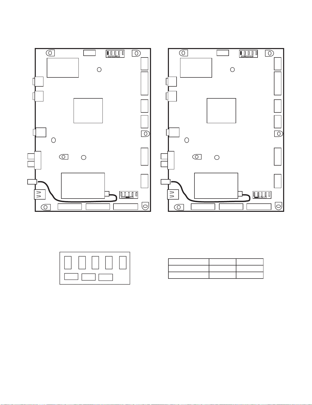
CHAPTER 6. PRINTED WIRING BOARD ASSEMBLIES
[1] MAIN Unit...............................................................6-1
CHAPTER 7. SCHEMATIC DIAGRAM
[1] DESCRIPTION OF SCHEMATIC DIAGRAM.........7-1
[2] MAIN Unit...............................................................7-2
CHAPTER 1. REMOVING OF MAJOR PARTS
[1] REMOVING OF MAJOR PARTS ...........................1-1
CHAPTER 2. ADJUSTMENT
[1] ADJUSTMENT PROCEDURE ...............................2-1
CHAPTER 3. TROUBLE SHOOTING TABLE
[1] TROUBLE SHOOTING TABLE..............................3-1
CHAPTER 4. MAJOR IC INFORMATIONS
[1] MAJOR IC INFORMATIONS..................................4-1
Parts marked with " " are important for maintaining the safety of the set. Be sure to replace these parts with specified ones for maintaining the
safety and performance of the set.
Parts Guide
This document has been published to be used for
after sales service only.
The contents are subject to change without notice.
Page 2
LC-32/37D62U SUPPLEMENT 1st
LC-32/37D62U SUPPLEMENT 1st
OUTLINE AND DIFFERENCES FROM BASE MODEL
Service Manual
OUTLINE
For this model, the main unit is changed.
When servicing the product, use this manual with the service manual LC-32/37D62U (S17A9LC32D62U) already issued.
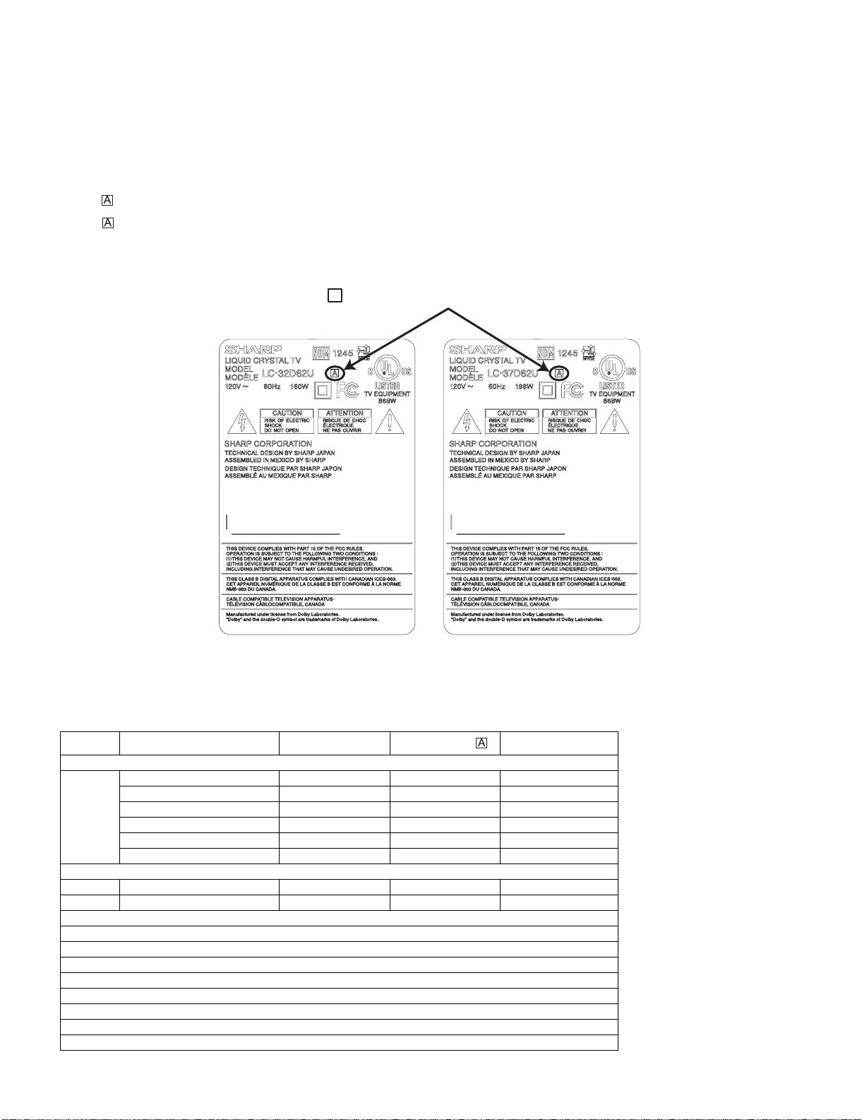
The new model can be identified with the following markings.
• The character is added at the end of the model name on the model label.
• The character is also added at the end of the model name on the number label (barcode label) of the packing case.
• The serial product numbers (in the 5th thru 9th digits) are 51112 and on.
MAIN unit change model
A mark on the right side of the model name
HINDPC568WJSA
LC-32D62U LABEL2-U
LIST OF CHANGED PARTS
Ref. No. Description LC-32/37D62U
PRINTED WIRING BOARD ASSEMBLIES
R/C, LED Unit DUNTKD909FM02 ← —
KEY Unit DUNTKD910FM02 ← —
MAIN Unit DUNTKE028FM06 DUNTKE230FM06 Some parts changed
TERMINAL Unit DUNTKD999FM07 ← —
POWER Unit RDENCA203WJQZ ← —
LCD PANEL
32”LCD Panel Module Unit R1LK315D3LZ10Z ← —
37”LCD Panel Module Unit R1LK370D3LZ20Z ← —
MAIN Unit
Please refer to a Parts list
CABINET AND MECHANICAL PARTS
Please refer to a Parts list
PACKING PARTS AND ACCESSORIES
Please refer to a Parts list
LC-32/37D62U
HINDPC569WJSA
LC-37D62U LABEL2-U
Note
i
Page 3
LC-32/37D62U SUPPLEMENT 1st
LC-32/37D62U SUPPLEMENT 1st
SAFETY PRECAUTION
Service Manual
IMPORTANT SERVICE SAFETY PRECAUTION
Service work should be performed only by qualified service technicians who are thoroughly familiar with all safety checks and the
servicing guidelines which follow:
WARNING
1. For continued safety, no modification of any circuit should be
attempted.
2. Disconnect AC power before servicing.
CAUTION: FO R C O N T INUED PROTECTION
AGAINST A RISK OF FIRE REPLACE ONLY WITH
SAME TYPE FUSE.
F701 (125V 8A)
F4702 (250V 6.3A)
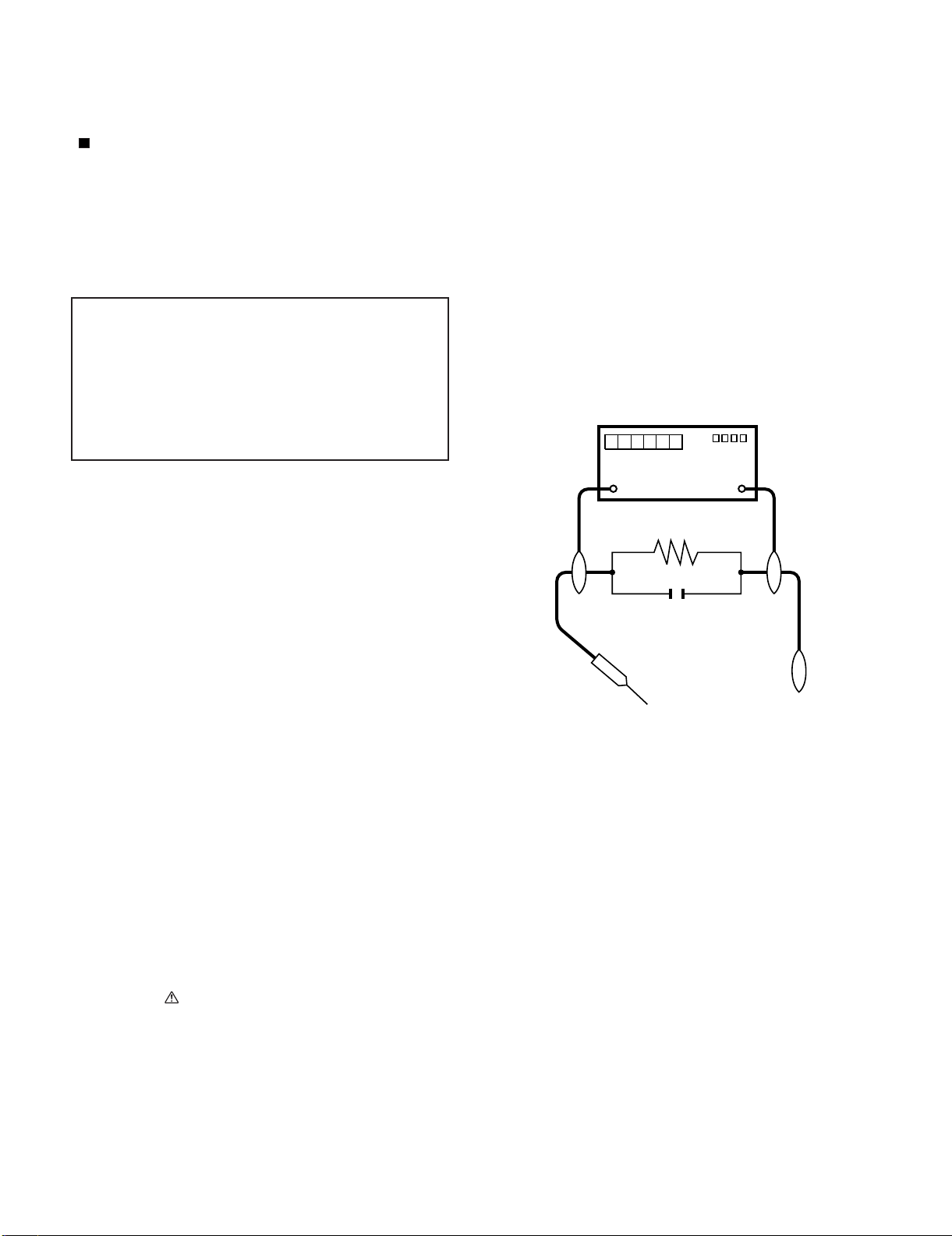
• Use an AC voltmeter having with 5000 ohm per volt, or higher, sensitivity or measure the AC voltage drop across the resistor.
• Connect the resistor connection to all exposed metal parts having a
return to the chassis (antenna, metal cabinet, screw heads, knobs
and control shafts, escutcheon, etc.) and measure the AC voltage
drop across the resistor.
All checks must be repeated with the AC cord plug connection
reversed. (If necessary, a nonpolarized adaptor plug must be used
only for the purpose of completing these checks.)
Any reading of 0.75 Vrms (this corresponds to 0.5 mA rms AC.) or
more is excessive and indicates a potential shock hazard which
must be corrected before returning the monitor to the owner.
DVM
BEFORE RETURNING THE RECEIVER (Fire &
Shock Hazard)
Before returning the receiver to the user, perform the following
safety checks:
3. Inspect all lead dress to make certain that leads are not pinched,
and check that hardware is not lodged between the chassis and
other metal parts in the receiver.
4. Inspect all protective devices such as non-metallic control knobs,
insulation materials, cabinet backs, adjustment and compartment
covers or shields, isolation resistor-capacitor networks, mechanical
insulators, etc.
5. To be sure that no shock hazard exists, check for leakage current in
the following manner.
• Plug the AC cord directly into a 120 volt AC outlet.
• Using two clip leads, connect a 1.5k ohm, 10 watt resistor paralleled by a 0.15µF capacitor in series with all exposed metal cabinet
parts and a known earth ground, such as electrical conduit or electrical ground connected to an earth ground.
///////////////////////////////////////////////////////////////////////////////////////////////////////////////////////////////////////////////////////////////////////////////////////////////////////////////////////////////////////////
TO EXPOSED
METAL PARTS
AC SCALE
1.5k ohm
10W
0.15µF
TEST PROBE
CONNECT TO
KNOWN EARTH
GROUND
SAFETY NOTICE
Many electrical and mechanical parts in LCD color television have
special safety-related characteristics.
These characteristics are often not evident from visual inspection, nor
can protection afforded by them be necessarily increased by using
replacement components rated for higher voltage, wattage, etc.
Replacement parts which have these special safety characteristics are
identified in this manual; electrical components having such features
are identified by " " and shaded areas in the Replacement Parts List
and Schematic Diagrams.
///////////////////////////////////////////////////////////////////////////////////////////////////////////////////////////////////////////////////////////////////////////////////////////////////////////////////////////////////////////
For continued protection, replacement parts must be identical to those
used in the original circuit.
The use of a substitute replacement parts which do not have the same
safety characteristics as the factory recommended replacement parts
shown in this service manual, may create shock, fire or other hazards.
ii
Page 4
LC-32/37D62U SUPPLEMENT 1st
PRECAUTIONS A PRENDRE LORS DE LA REPARATION
Ne peut effectuer la réparation qu' un technicien spécialisé qui s'est parfaitement accoutumé à toute vérification de sécurité et aux
conseils suivants.
•
AVERTISSEMENT
1.
N'entreprendre aucune modification de tout circuit. C'est dangereux.
2.
Débrancher le récepteur avant toute réparation.
PRECAUTION: POUR LA PROTECTION CONTINUE CONTRE LES RISQUES D'INCENDIE,
REMPLACER LE FUSIBLE
F701 (125V 8A)
F4702 (250V 6.3A)
VERIFICATIONS CONTRE L'INCEN-DIE ET LE
CHOC ELECTRIQUE
Avant de rendre le récepteur à l'utilisateur, effectuer les vérifications suivantes.
Inspecter tous les faisceaux de câbles pour s'assurer que les fils
3.
ne soient pas pincés ou qu'un outil ne soit pas placé entre le châssis et les autres pièces métalliques du récepteur.
4.
Inspecter tous les dispositifs de protection comme les boutons de
commande non-métalliques, les isolants, le dos du coffret, les couvercles ou blindages de réglage et de compartiment, les réseaux
de résistancecapacité, les isolateurs mécaniques, etc.
5.
S'assurer qu'il n'y ait pas de danger d'électrocution en vérifiant la
fuite de courant, de la facon suivante:
•
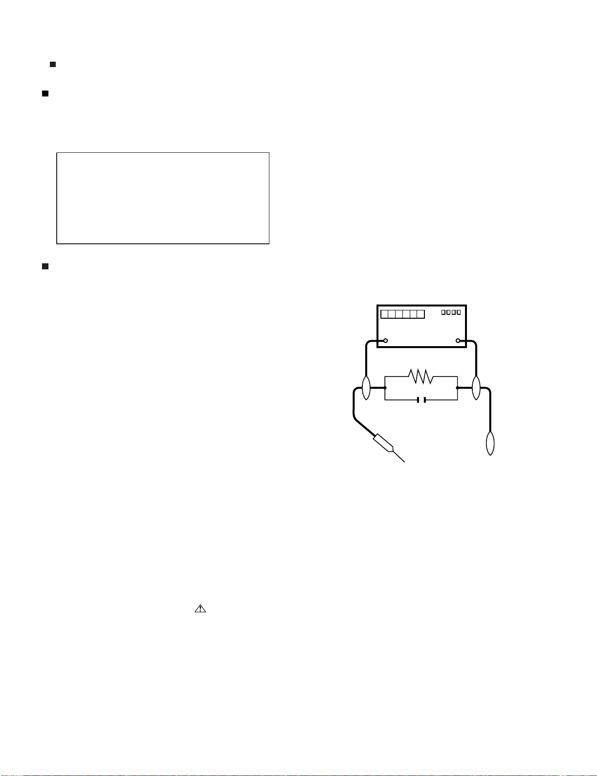
Brancher le cordon d'alimentation directem-ent à une prise de courant de 120V. (Ne pas utiliser de transformateur d'isolation pour
cet essai).
A l'aide de deux fils à pinces, brancher une résistance de 1.5 kΩ
10 watts en parallèle avec un condensateur de 0.15µF en série
avec toutes les pièces métalliques exposées du coffret et une terre
connue comme une conduite électrique ou une prise de terre
branchée à la terre.
•
Utiliser un voltmètre CA d'une sensibilité d'au moins 5000Ω/V pour
mesurer la chute de tension en travers de la résistance.
•
Toucher avec la sonde d'essai les pièces métalliques exposées qui
présentent une voie de retour au châssis (antenne, coffret métallique, tête des vis, arbres de commande et des boutons, écusson,
etc.) et mesurer la chute de tension CA en-travers de la résistance.
Toutes les vérifications doivent être refaites après avoir inversé la
fiche du cordon d'alimentation. (Si nécessaire, une prise
d'adpatation non polarisée peut être utilisée dans le but de terminer ces vérifications.)
La tension de pointe mesurèe ne doit pas dépasser 0.75V (correspondante au courant CA de pointe de 0.5mA).
Dans le cas contraire, il y a une possibilité de choc électrique qui
doit être supprimée avant de rendre le récepteur au client.
DVM
ECHELLE CA
1.5k ohm
10W
µ
F
0.15
SONDE D'ESSAI
AUX PIECES
METALLIQUES
EXPOSEES
/////////////////////////////////////////////////////////////////////////////////////////////////////////////////////////////////////////////////////////////////////////////////////////////////////////////////////////////////////////////
BRANCHER A UNE
TERRE CONNUE
AVIS POUR LA SECURITE
De nombreuses pièces, électriques et mécaniques, dans les téléviseur ACL présentent des caractéristiques spéciales relatives à la sécurité, qui ne sont souvent pas évidentes à vue. Le degré de protection ne peut pas être nécessairement augmentée en utilisant des
pièces de remplacement étalonnées pour haute tension, puissance,
etc.
Les pièces de remplacement qui présentent ces caractéristiques sont
identifiées dans ce manuel; les pièces électriques qui présentent ces
particularités sont identifiées par la marque " " et hachurées dans la
liste des pièces de remplacement et les diagrammes schématiques.
/////////////////////////////////////////////////////////////////////////////////////////////////////////////////////////////////////////////////////////////////////////////////////////////////////////////////////////////////////////////
Pour assurer la protection, ces pièces doivent être identiques à celles
utilisées dans le circuit d'origine. L'utilisation de pièces qui n'ont pas
les mêmes caractéristiques que les pièces recommandées par l'usine,
indiquées dans ce manuel, peut provoquer des électrocutions, incendies, radiations X ou autres accidents.
iii
Page 5
LC-32/37D62U SUPPLEMENT 1st
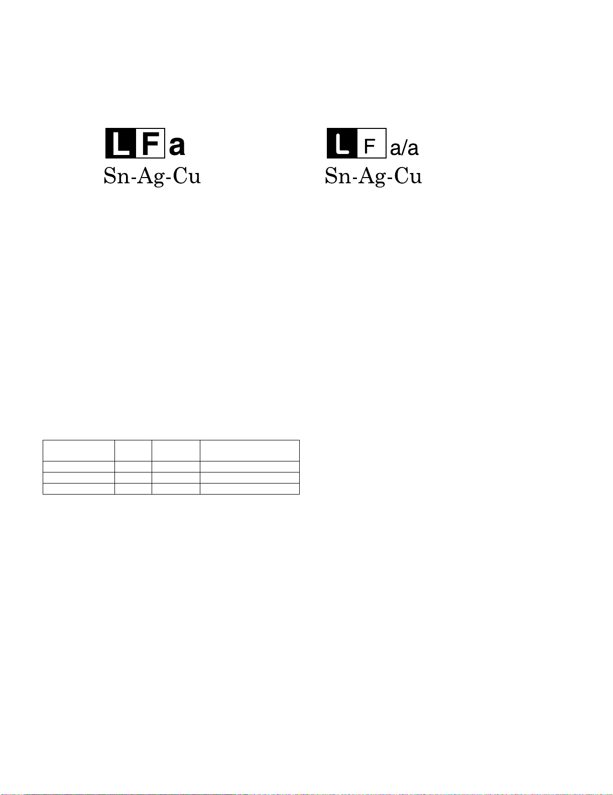
PRECAUTIONS FOR USING LEAD-FREE SOLDER
Employing lead-free solder
• “PWBs” of this model employs lead-free solder. The LF symbol indicates lead-free solder, and is attached on the PWBs and service manuals. The
alphabetical character following LF shows the type of lead-free solder.
Example:
Indicates lead-free solder of tin, silver and copper. Indicates lead-free solder of tin, silver and copper.
Using lead-free wire solder
• When fixing the PWB soldered with the lead-free solder, apply lead-free wire solder. Repairing with conventional lead wire solder may cause damage or accident due to cracks.
As the melting point of lead-free solder (Sn-Ag-Cu) is higher than the lead wire solder by 40 °C, we recommend you to use a dedicated soldering
bit, if you are not familiar with how to obtain lead-free wire solder or soldering bit, contact our service station or service branch in your area.
Soldering
• As the melting point of lead-free solder (Sn-Ag-Cu) is about 220 °C which is higher than the conventional lead solder by 40 °C, and as it has poor
solder wettability, you may be apt to keep the soldering bit in contact with the PWB for extended period of time. However, Since the land may be
peeled off or the maximum heat-resistance temperature of parts may be exceeded, remove the bit from the PWB as soon as you confirm the
steady soldering condition.
Lead-free solder contains more tin, and the end of the soldering bit may be easily corroded. Make sure to turn on and off the power of the bit as
required.
If a different type of solder stays on the tip of the soldering bit, it is alloyed with lead-free solder. Clean the bit after every use of it.
When the tip of the soldering bit is blackened during use, file it with steel wool or fine sandpaper.
• Be careful when replacing parts with polarity indication on the PWB silk.
Lead-free wire solder for servicing
PARTS CODE
ZHNDAi123250E BL J φ0.3mm 250g (1roll)
ZHNDAi126500E BK J φ0.6mm 500g (1roll)
ZHNDAi12801KE BM J φ1.0mm 1kg (1roll)
PRICE
RANK
PART
DELIVERY
DESCRIPTION
iv
Page 6
LC-32/37D62U SUPPLEMENT 1st
LC-32/37D62U SUPPLEMENT 1st
CHAPTER 1. REMOVING OF MAJOR PARTS
Service Manual
[1] REMOVING OF MAJOR PARTS
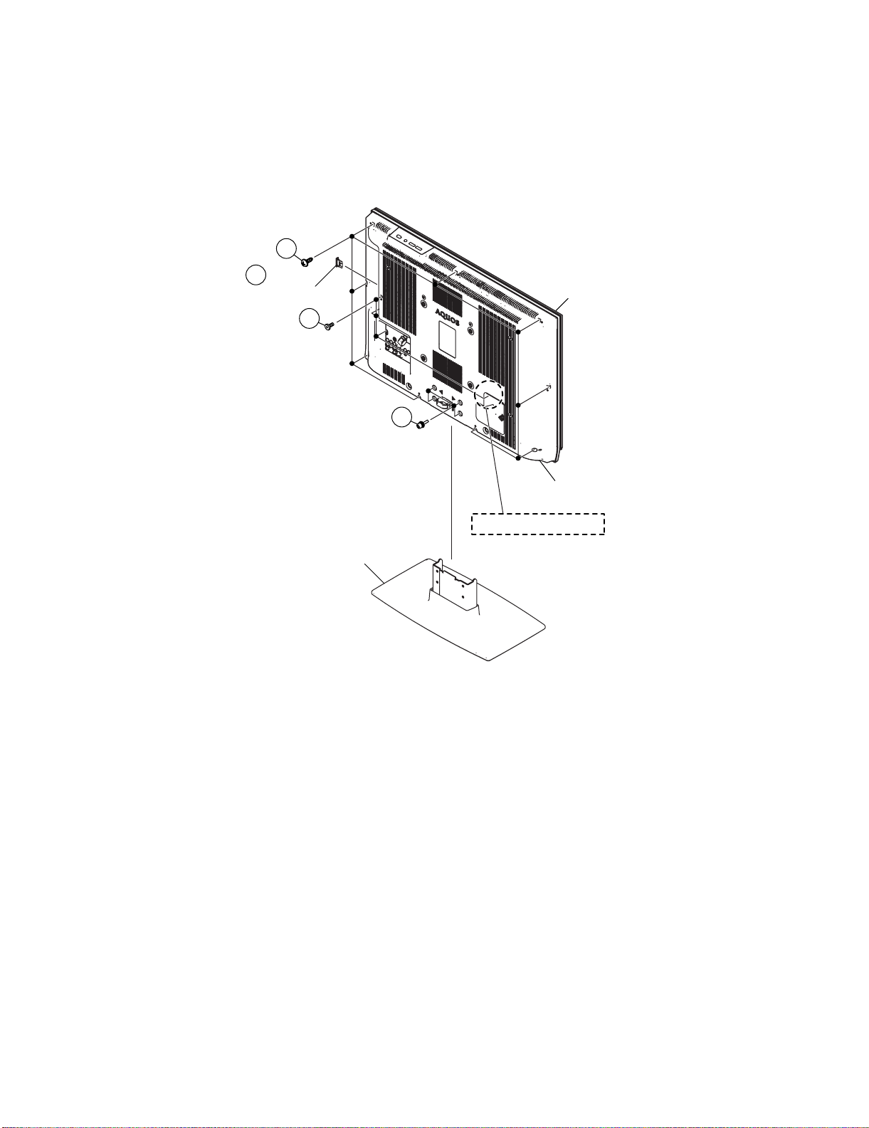
1. Remove the SD Card Cover.
2. Remove the 4 lock screws and detach the Stand Base Ass'y.
3. Remove the 9 lock screws, 3 lock screws and detach the Rear Cabinet. (LC-32D62U)
Remove the 9 lock screws, 4 lock screws and detach the Rear Cabinet. (LC-37D62U)
3
1
SD Card Cover
3
2
Front Cabinet
Stand Base Ass'y
Rear Cabinet
LC-37D62U Only
1 – 1
Page 7
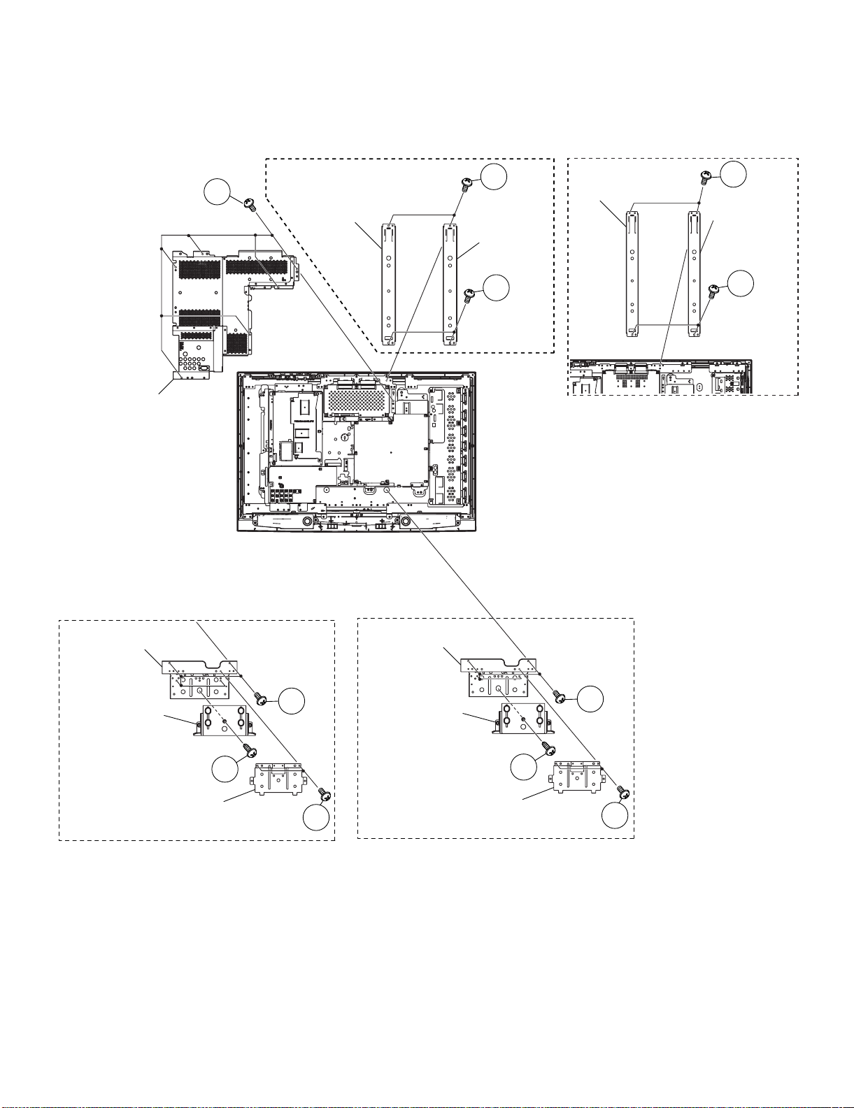
4. Remove the 2 lock screws and detach the Stand Assist Angle.
5. Remove the 4 lock screws and detach the Center Angle-L and R.
6. Remove the 1 lock screw and detach the Stand Area Cover.
7. Remove the 4 lock screws and detach the Stand Fix Angle.
8. Remove the 6 lock screws and detach the MAIN Shield.
LC-32/37D62U SUPPLEMENT 1st
MAIN Shield
LC-32D62U
5
8
Center Angle-R
Center Angle-L
5
LC-37D62U
Center Angle-R
5
Center Angle-L
5
Stand Fix Angle
Stand Area Cover
Stand Assist Angle
6
LC-37D62U
7
4
Stand Fix Angle
Stand Area Cover
LC-32D62U
7
6
Stand Assist Angle
4
1 – 2
Page 8
LC-32/37D62U SUPPLEMENT 1st
9. Disconnect all the connectors from all the PWBs.
10.Remove the Top Cover Ass'y. Remove the 2 lock screws from the Top Cover Ass'y and detach the KEY Unit.
10
Top Cover
[KM]
KEY Unit
10
9
9
[F-RCA wire]
[KM]
[SP]
[LP]
[LV]
[LB]
[PH]
[PD]
[SA][FC][MA]
[RA]
[CN5] (32D62U)
[CN4] (37D62U)
[CN1]
[CN2] (37D62U)
[CN4] (32D62U)
[CN3] (37D62U)
[CN2] (32D62U)
[PH]
[PD]
9
[LB] (32D62U)
[LA]
9
[LA]
[LB] (37D62U)
1 – 3
Page 9
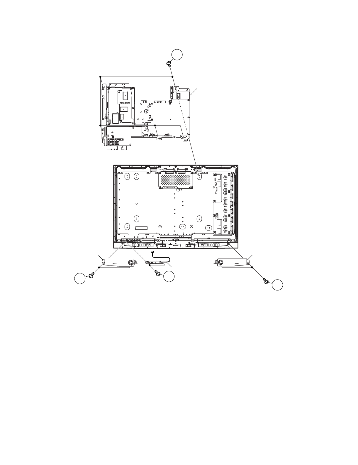
11.Remove the 4 lock screws and detach the Speaker-L and R.
12.Remove the 2 lock screws and detach the R/C, LED Unit.
13.Remove the 5 lock screws and detach the Tray Chassis.
LC-32/37D62U SUPPLEMENT 1st
13
Tray Chassis
Speaker-R
11
Speaker-L
R/C, LED Unit
12
11
1 – 4
Page 10
LC-32/37D62U SUPPLEMENT 1st
14.Remove the 2 lock screws and detach the Jack Angle.
15.Remove the 6 lock screws and detach the POWER Unit.
16.Remove the 4 lock screws and detach the TERMINAL Unit.
17.Remove the 5 lock screws, 2 lock rivets and detach the MAIN PWB Radiator and MAIN Unit.
MAIN PWB Radiator
17
MAIN Unit
14
17
17
15
POWER Unit
Jack Angle
16
TERMINAL Unit
1 – 5
Page 11
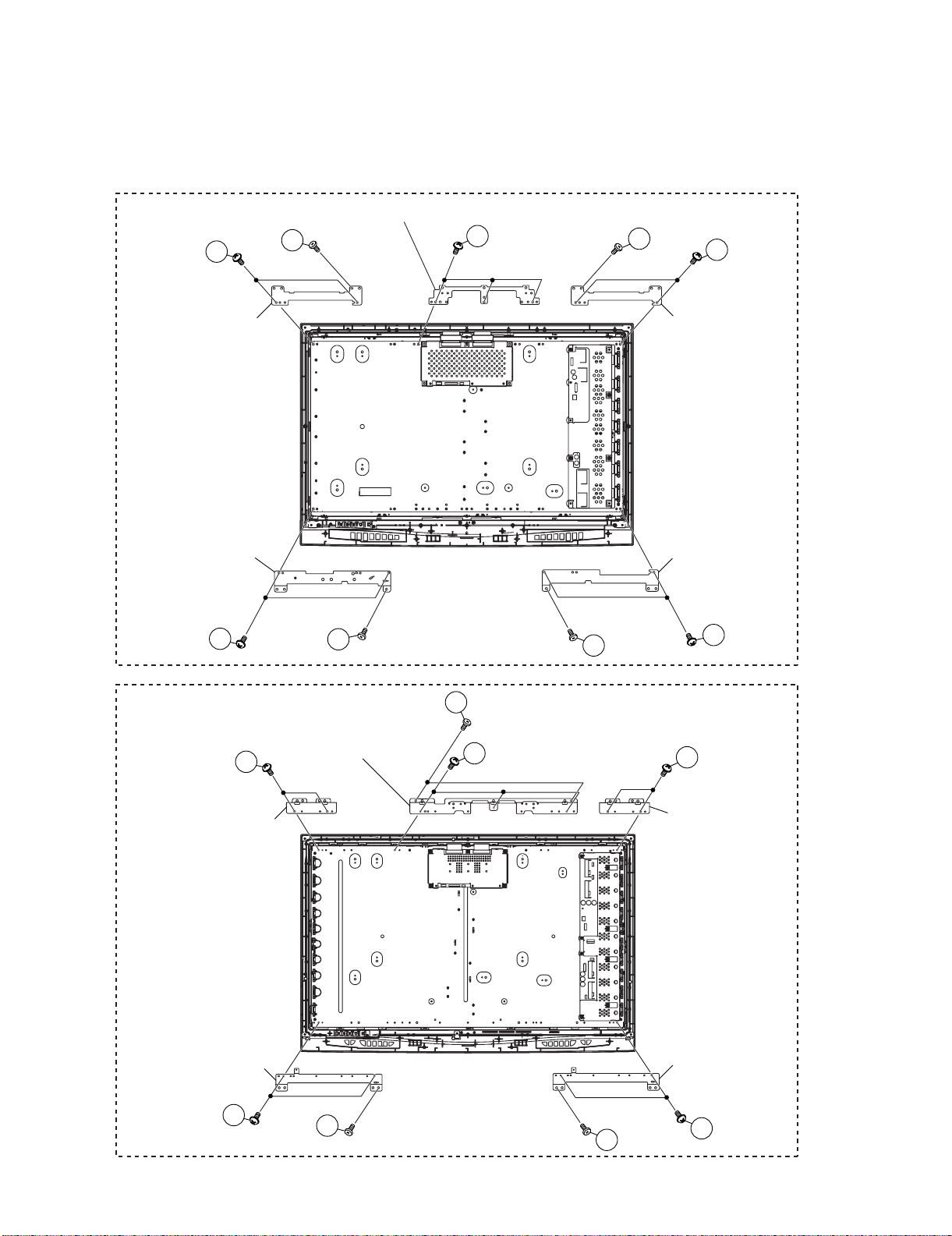
18.Remove the 6 lock screws and detach the Rug Angle Top-L and R. (LC-32D62U)
Remove the 4 lock screws and detach the Rug Angle Top-L and R. (LC-37D62U)
19.Remove the 6 lock screws and detach the Rug Angle Bottom-L and R.
20.Remove the 3 lock screws and detach the Chassis Fix Angle Top. (LC-32D62U)
Remove the 5 lock screws and detach the Chassis Fix Angle Top. (LC-37D62U)
21.Remove the LCD Panel Module.
LC-32/37D62U SUPPLEMENT 1st
LC-32D62U
18
Rug Angle Top-R
Rug Angle Bottom-R
19
18
Chassis Fix Angle Top
19
20
19
18
Rug Angle Bottom-L
18
Rug Angle Top-L
19
LC-37D62U
Rug Angle Top-R
Rug Angle Bottom-R
19
18
Chassis Fix Angle Top
19
20
20
19
18
Rug Angle Top-L
Rug Angle Bottom-L
19
1 – 6
Page 12
LC-32/37D62U SUPPLEMENT 1st
LC-32/37D62U SUPPLEMENT 1st
CHAPTER 2. ADJUSTMENT
Service Manual
[1] ADJUSTMENT PROCEDURE
The adjustment values are set to the optimum conditions at the factory before shipping. If a value should become improper or an adjustment is
required due to part replacement, make an adjustment according to the following procedure.
1. After replacement of any PWB unit and/or IC for repair, please note the following.
• When replacing the following units, make sure to prepare the new units loaded with updated software.
MAIN Unit: DUNTKE230FM06
2. Upgrading of each microprocessor software
CAUTION: Never “POWER OFF” the unit when software upgrade is ongoing.
Otherwise the system may be damaged beyond recovery.
2.1. Software version upgrade
The model employs the following software.
•Main software
• Monitor microprocessor software.
The main software and the monitor microprocessor software can be upgraded by using a general-purpose USB Memory.
The followings are the procedures for upgrading, explained separately for the main software, and the monitor microprocessor software.
2.2. Main software version upgrade
2.2.1 Get ready before you start
• USB Memory of 128MB or higher capacity.
• PC running on Windows 98/98SE/ME/2000/XP operating system.
• USB Memory reader/writer or PC with a USB port.
• The file system of a USB memory is FAT. (FAT32 is not applied)
• Use the USB memory without other functions. (lock and memory reader...etc)
2.2.2 Preparations
To upgrade the main software, it is necessary to get ready the USB Memory for version upgrade before you start.
Follow the steps below and create the USB Memory for version upgrade.
1. Copy the file D62UAxxx.USB (named temporarily) for version upgrade to the root directory (folder) of the USB Memory.
NOTE: In the USB Memory drive, do not store other folders or unrelated files, or more than one file for version upgrade.
Now the USB Memory for version upgrade is ready.
2.2.3 How to upgrade the software
1. Unplug the AC cord.
2. Insert the USB Memory for version upgrade (prepared as above) into the service socket.
3. Plug in the AC cord with power button pressed down after 5 seconds, unpress the power button.
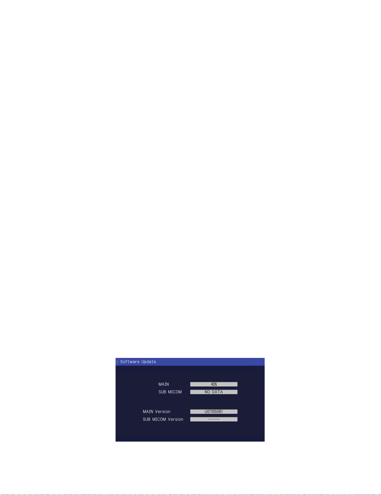
4. After the unit startup, the system upgrade screen as shown below appears within 20-40 seconds.
D62U
2 – 1
Page 13
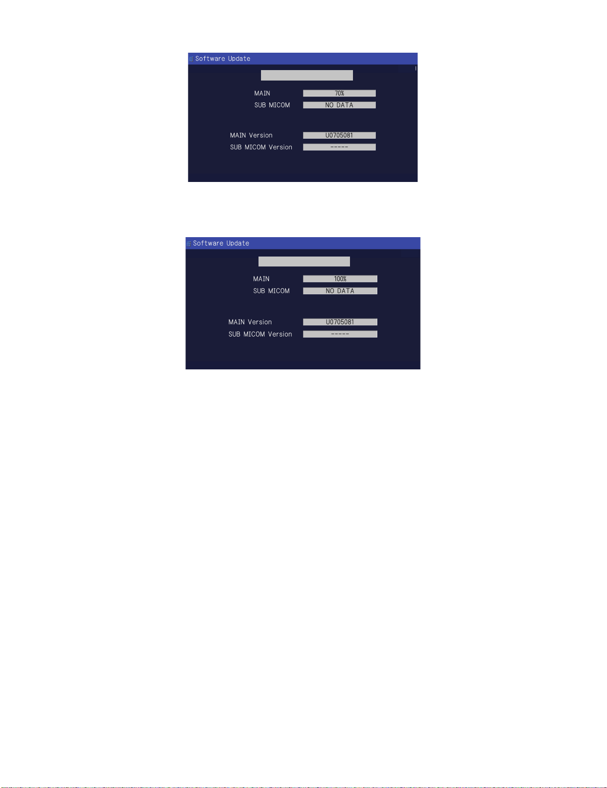
5. Even a single failure in the process will trigger the upgrade failure screen.
LC-32/37D62U SUPPLEMENT 1st
UPGRADE FAILURE
NOTE: In the event of a failure, repeat the upgrade process. If the process repeatedly fails, it is likely that the hardware need fixing.
6. Upon completion of the whole process, the upgrade success screen as shown below appears. You can check the new software version on this
screen. The version information appears after the upgrade is complete.
UPGRADE SUCCESS
D62U
D62U
7. Unplug the AC cord and remove the USB Memory for version upgrade.
8. Now the software version upgrade is complete.
NOTE: When you are done with the software version upgrade, start the set, go to the top page of the adjustment process screen and check the main
software version information.
2 – 2
Page 14
LC-32/37D62U SUPPLEMENT 1st
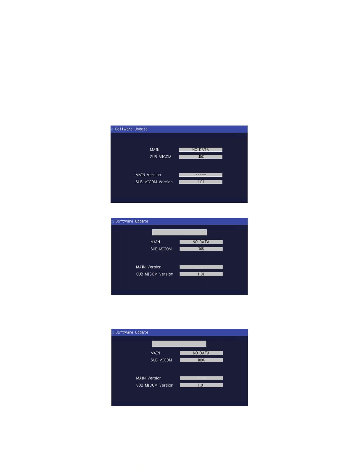
2.3. Monitor microprocessor software version upgrade
Create the USB memory for monitor microprocessor software version upgrade in the same manner as explained in the “Main software version
upgrade”.
Copy the file D62UVAxx.USB and D62UMxxx.BIN (named temporarily) for monitor microprocessor software version upgrade to the USB memory.
2.3.1 How to upgrade the software
1. Unplug the AC cord.
2. Insert the USB memory for version upgrade (prepared as above) into the service socket.
3. Plug in the AC cord with power button pressed down.
4. After 5 seconds, unpress the power button.
CAUTION: • The moment this operation is done, the upgrading of the monitor microprocessor software starts. While the upgrade is ongoing, never
power off the unit. Otherwise the upgrade will fail and the system may be serious damaged beyond recovery (inability to start).
• After the monitor microprocessor software is upgraded, also perform the 'Industry Init'.
5. After the unit startup, the upgrade starts. The power led will blink continuously. Also, an upgrade screen will be shown during a minor upgrade.
D62U
6. If the upgrade fails, power led will stop blinking. Also, the upgrade failure screen will be shown if upgrade screen was shown at 5.
UPGRADE FAILURE
NOTE: In the event of a transient failure, upgrade will be automatically retried up to three times. If the process repeatedly fails, hardware may be the
cause.
7. Up on completion of the whole process, power and OPC LED will blink alternately. Also, the upgrade success screen will be shown if upgrade
screen was shown at 5.
UPGRADE SUCCESS
D62U
D62U
8. Unplug the AC cord and remove the USB Memory for version upgrade.
9. Now the software version upgrade is complete.
NOTE: When you are done with the software version upgrade, start the set, go to the top page of the adjustment process screen and check the mon-
itor microprocessor software version information and panel size information.
2 – 3
Page 15
LC-32/37D62U SUPPLEMENT 1st
3. Entering and exiting the adjustment process mode
1) Before entering the adjustment process mode, the AV position RESET in the video adjustment menu.
2) While holding down the “VOL (–)” and “INPUT” keys at a time, plug in the AC cord of the main unit to turn on the power.
The letter “<K>” appears on the screen.
3) Next, hold down the “VOL (–)” and “CH ( )” keys at a time.
(The “VOL (–)” and “CH ( )” keys should be pressed and held until the display appears.)
Multiple lines of blue characters appearing on the display indicate that the unit is now in the adjustment process mode.
When you fail to enter the adjustment process mode (the display is the same as normal startup), retry the procedure.
4) To exit the adjustment process mode after the adjustment is done, unplug the AC cord from the outlet to make a forced shutdown. (When the
power was turned off with the remote controller, once unplug the AC cord and plug it again. In this case, wait 10 seconds or so before plugging.)
CAUTION: Use due care in handling the information described here lest your users should know how to enter the adjustment process mode. If the
4. Remote controller key operation and description of display in adjustment process mode
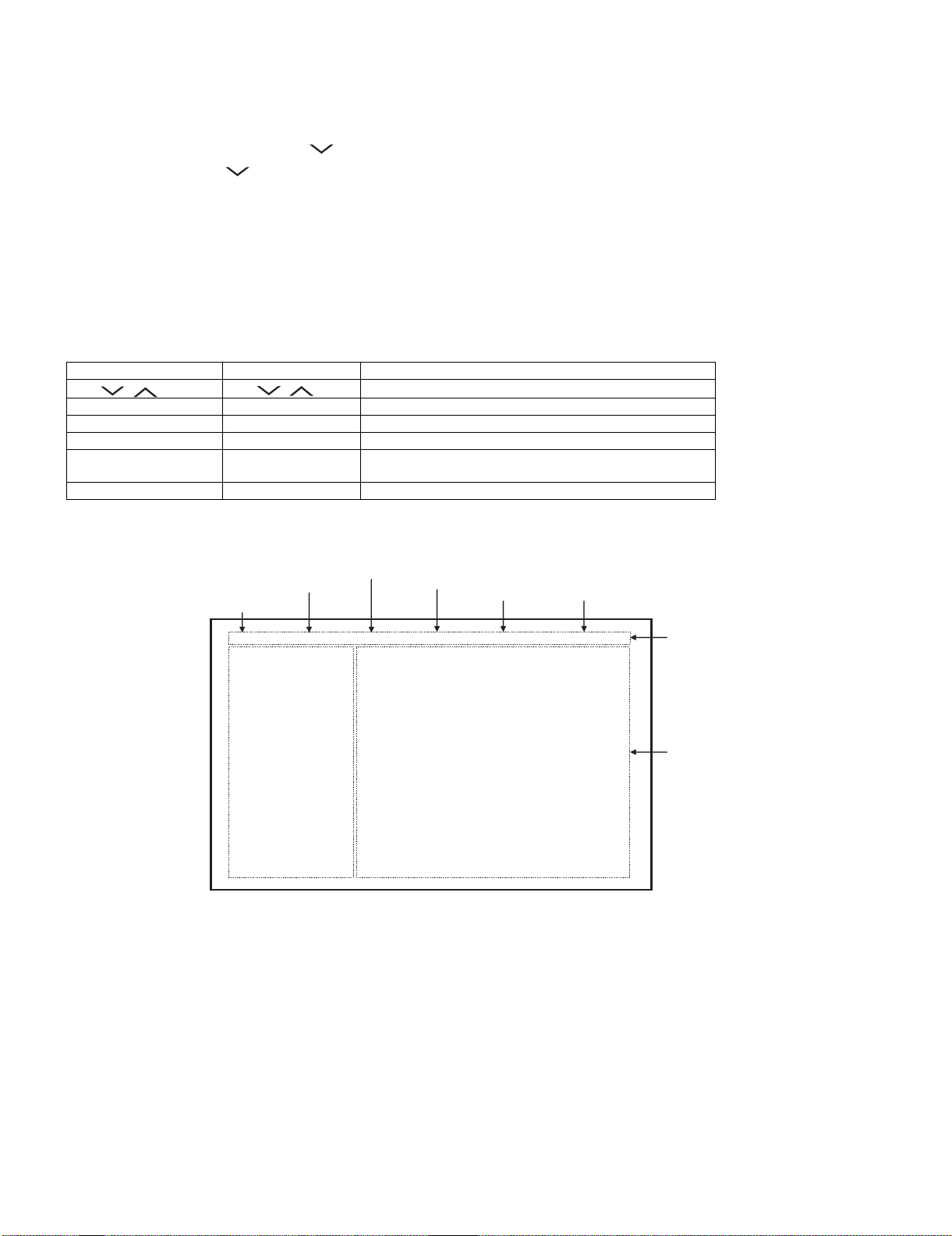
1) Key operation
Remote controller key Main unit key Function
CH ( / ) CH ( / )
VOL (+/–) VOL (+/–) Changing a selected item setting (+1/ –1)
Cursor (UP/DOWN) ————— Turing a page (PREVIOUS/NEXT)
Cursor (LEFT/RIGHT) ————— Changing a selected line setting (+10/ –10)
INPUT ————— Input switching (toggle switching)
ENTER ————— Executing a function
settings are tampered in this mode, unrecoverable system damage may result.
Moving an item (line) by one (UP/DOWN)
(TUNER→INPUT1→INPUT2→INPUT3→INPUT4→INPUT5)
*Input mode is switched automatically when relevant adjustment is started so far as the necessary input signal is available.
2) Description of display
(1) Current page/ (5) Destination
Total pages
1/32 [INFO] INPUT5 AUTO USA 46_UNDER
MAIN Version 1.00 (U 2007/07/11 RA)
BOOT Version D62U 1.01
Monitor Version 1.00 R
Monitor Boot Version 1.00
EQ DATA CHECKSUM ROM
TEMPERATURE 7B
LAMP ERROR 0
MONITOR ERR CAUSE
NORMAL STANDBY CAUSE
ERROR STANDBY CAUSE 1) 0 2) 0 3) 0
(2) Current page title
(3) Current selected input
(4) Current color system
0
00H 00M 00H 00M 00H 00M
4) 0 5) 0
00H 00M 00H 00M
(6) LCD Panel size/Speaker type
(LC-32D62U: 32_UNDER)
(LC-37D62U: 37_UNDER)
(7) Adjustment
process menu
header
(8) Parameters
2 – 4
Page 16
LC-32/37D62U SUPPLEMENT 1st
5. List of adjustment process mode menu
The character string in brackets [ ] will appear as a page title in the adjustment process menu header.
Page Line Item Description Remarks (adjustment detail, etc.)
1 [INFO]
1 MAIN Version Main software version
2BOOT Version
3 Monitor Version Monitor software version
4 Monitor BOOT Version
5 EQ DATA CHECKSUM Audio data checksum
6 TEMPERATURE Panel temperature
7 LAMP ERROR Number of termination due to lamp error
8 MONITOR ERR CAUSE
9 NORMAL STANDBY CAUSE Refer to *1 under the list for details
10 ERROR STANDBY CAUSE Refer to *2 under the list for details
2 [INIT]
1 INDUSTRY INIT (+Cause)
2 INDUSTRY INIT Initialization to factory settings
3 HOTELMODE Hotel mode
4 Center Acutime Accumulated main operation time
5 RESET Reset
6 Backlight Acutime Accumulated monitor operation time
7 RESET Reset
8 LAMP ERROR RESET Reset LAMP ERROR
9 VIC XPOS X-coordinate setting for VIC READ
10 VIC YPOS Y-coordinate setting for VIC READ
11 VIC COLOR Collected color data setting for VIC READ
12 VIC SIGNAL TYPE Signal type setting for VIC READ
13 VIC READ Picture level acquisition function Level appears in green on the upper right
3 [N358MAIN]
1 N358 ALL ADJ (INPUT1) CVBS and TUNER signal level adjustment
2 N358 ALL ADJ (INPUT2)
3 N358 MAIN ADJ (INPUT1) CVBS signal level adjustment
4 N358 MAIN ADJ (INPUT2)
5 TUNER DAC ADJ TUNER signal level adjustment
6 VCOM ADJ VCOM adjustment value
7 N358 CONTRAST A_GAIN
8 N358 CONTRAST D_GAIN
9 N358 CONTRAST OFFSET
10 TUNER CONTRAST A_GAIN
11 TUNER CONTRAST D_GAIN
4 [TUNER TEST]
1 TUNER VCHIP TEST (69ch) Tuning test and VCHIP test (69 ch)
2 TUNER VCHIP TEST (7ch) Tuning test and VCHIP test (7 ch)
3 TUNER VCHIP TEST (10ch) Tuning test and VCHIP test (10 ch)
4 TUNER VCHIP TEST (15ch) Tuning test and VCHIP test (15 ch)
5 INSPECT USB TERM
6 HDMI CEC TEST
5 [COMP15KMAIN]
1 COMP15K ADJ (INPUT1) Component 15K picture level adjustment (main)
2 COMP15K ADJ (INPUT3)
3 COMP15K Y A_GAIN
4 COMP15K Cb A_GAIN
5 COMP15K Cr A_GAIN
6 COMP15K Y D_GAIN
7 COMP15K Cb D_GAIN
8 COMP15K Cr D_GAIN
9 COMP15K Y OFFSET Y OFFSET adjustment value
10 COMP15K Cb OFFSET Cb OFFSET adjustment value
11 COMP15K Cr OFFSET Cr OFFSET adjustment value
2 – 5
Page 17
LC-32/37D62U SUPPLEMENT 1st
Page Line Item Description Remarks (adjustment detail, etc.)
6 [HDTV]
1 COMP33K ADJ (INPUT1) Component 33K picture level adjustment (main)
2 COMP33K ADJ (INPUT3)
3 COMP33K Y A_GAIN
4 COMP33K Cb A_GAIN
5 COMP33K Cr A_GAIN
6 COMP33K Y OFFSET Y OFFSET adjustment value
7 COMP33K Cb OFFSET Cb OFFSET adjustment value
8 COMP33K Cr OFFSET Cr OFFSET adjustment value
7
1 COMP67K ADJ (INPUT1)
2 COMP67K ADJ (INPUT3)
3 COMP67K Y A_GAIN
4 COMP67K Cb A_GAIN
5 COMP67K Cr A_GAIN
6 COMP67K Y OFFSET
7 COMP67K Cb OFFSET
8 COMP67K Cr OFFSET
8 [M GAMMA IN]
1 LEV1 Standard value 1 Adjustment gradation setting.
2 LEV2 Standard value 2
3 LEV3 Standard value 3
4 LEV4 Standard value 4
5 LEV5 Standard value 5
6 LEV6 Standard value 6
9 [M GAMMA R1]
1 MG1R WB adjustment Point 1, R adjustment value Parameter for six-point adjustment
2 MG1G WB adjustment Point 1, G adjustment value
3 MG1B WB adjustment Point 1, B adjustment value
4 MG2R WB adjustment Point 2, R adjustment value
5 MG2G WB adjustment Point 2, G adjustment value
6 MG2B WB adjustment Point 2, B adjustment value
7 MG3R WB adjustment Point 3, R adjustment value
8 MG3G WB adjustment Point 3, G adjustment value
9 MG3B WB adjustment Point 3, B adjustment value
10 [M GAMMA R4]
1 MG4R WB adjustment Point 4, R adjustment value Parameter for six-point adjustment
2 MG4G WB adjustment Point 4, G adjustment value
3 MG4B WB adjustment Point 4, B adjustment value
4 MG5R WB adjustment Point 5, R adjustment value
5 MG5G WB adjustment Point 5, G adjustment value
6 MG5B WB adjustment Point 5, B adjustment value
7 MG6R WB adjustment Point 6, R adjustment value
8 MG6G WB adjustment Point 6, G adjustment value
9 MG6B WB adjustment Point 6, B adjustment value
11 [SOUND 1]
1 Audio Switch
2 Flat Mode
3 ADC Volume 1
4 ADC Volume 2
5 ADC Volume 3
6 ADC Volume 4
7 ADC Volume 5
8 ADC Volume 6
9 LR Fanc Vol AIN
10 LR Fanc Vol HDMI
11 LR Fanc Vol ATV
12 LR Fanc Vol DTV
13 Input Trim
2 – 6
Page 18
LC-32/37D62U SUPPLEMENT 1st
Page Line Item Description Remarks (adjustment detail, etc.)
12 [SOUND 2]
1Eala
2 Eala Bass
3 Eala D
4 Eala Surround Gain
5 Eala Bass Surround Gain
6 Eala Bass LPF Fc
7 Eala Bass LPF Gain
8 Eala Bass Treble HPF F0
9 Eala Bass Treble HPF Gain
10 Eala Bass Output Gain
11 Eala Bass Attack Time
12 Eala Bass Release Time
13 [SOUND 3]
1 Eala D Surround Width
2 Eala D Bass Enhancer
3 Eala D Dialogue Boost
4 Eala D Bass Doubler
5 Eala D F0
6 Eala D DRC Ratio
7 Eala D DRC Threshold Level
14 [SOUND 4]
1EQ_MODE
2 PEQ1_F0
3 PEQ1_Q
4 PEQ1_GAIN
5 PEQ2_F0
6 PEQ2_Q
7 PEQ2_GAIN
8 PEQ3_F0
9 PEQ3_Q
10 PEQ3_GAIN
15 [SOUND 5]
1 PEQ4_F0
2 PEQ4_Q
3 PEQ4_GAIN
4 PEQ5_F0
5 PEQ5_Q
6 PEQ5_GAIN
7 PEQ6_F0
8 PEQ6_Q
9 PEQ6_GAIN
10 PEQ7_F0
11 PEQ7_Q
12 PEQ7_GAIN
16 [SOUND 6]
1 Output Trim
2 Clipper Level
3 Sub Vol Default
4 Sub Vol Eala
5 Sub Vol Eala Bass
6 Sub Vol Eala D
7 Sub Vol Eala Bass D
8 SW Fanc Vol AIN
9 SW Fanc Vol HDMI
10 SW Fanc Vol ATV
11 SW Fanc Vol DTV
2 – 7
Page 19
LC-32/37D62U SUPPLEMENT 1st
Page Line Item Description Remarks (adjustment detail, etc.)
17 [SOUND 7]
1 BE ATT
2 BASS VOL0 MIN
3 BASS VOL0 CENTER
4 BASS VOL0 MAX
5 BASS VOL60 MIN
6 BASS VOL60 CENTER
7 BASS VOL60 MAX
8 BASS CENTER ATT
18 [SOUND 8]
1 TREBLE VOL0 MIN
2 TREBLE VOL0 CENTER
3 TREBLE VOL0 MAX
4 TREBLE VOL60 MIN
5 TREBLE VOL60 CENTER
6 TREBLE VOL60 MAX
7 TREBLE CENTER ATT
19 [M PWM]
1 PANNEL SELECT
2PWM
3PWN FREQ
4 PWM DUTY
5OSC FREQ
6 OSC DUTY
20 [M BRI DA1]
1 BRIGHTNESS DA0
2 BRIGHTNESS DA1
3 BRIGHTNESS DA2
4 BRIGHTNESS DA3
5 BRIGHTNESS DA4
6 BRIGHTNESS DA5
7 BRIGHTNESS DA6
8 BRIGHTNESS DA7
9 BRIGHTNESS DA8
10 BRIGHTNESS DA9
11 BRIGHTNESS DA10
12 BRIGHTNESS DA11
21 [M BRI DA2]
1 BRIGHTNESS DA12
2 BRIGHTNESS DA13
3 BRIGHTNESS DA14
4 BRIGHTNESS DA15
5 BRIGHTNESS DA16
6 BRIGHTNESS DA17
7 BRIGHTNESS DA18
8 BRIGHTNESS DA19
9 BRIGHTNESS DA20
10 BRIGHTNESS DA21
11 BRIGHTNESS DA22
22 [M BRI DA3]
1 BRIGHTNESS DA23
2 BRIGHTNESS DA24
3 BRIGHTNESS DA25
4 BRIGHTNESS DA26
5 BRIGHTNESS DA27
6 BRIGHTNESS DA28
7 BRIGHTNESS DA29
8 BRIGHTNESS DA30
9 BRIGHTNESS DA31
10 BRIGHTNESS DA32
2 – 8
Page 20
LC-32/37D62U SUPPLEMENT 1st
Page Line Item Description Remarks (adjustment detail, etc.)
23 [M ADL1]
1 OPC33 ADLEVEL 0
2 OPC33 ADLEVEL 1
3 OPC33 ADLEVEL 2
4 OPC33 ADLEVEL 3
5 OPC33 ADLEVEL 4
6 OPC33 ADLEVEL 5
7 OPC33 ADLEVEL 6
8 OPC33 ADLEVEL 7
9 OPC33 ADLEVEL 8
10 OPC33 ADLEVEL 9
11 OPC33 ADLEVEL 10
12 OPC33 ADLEVEL 11
24 [M ADL2]
1 OPC33 ADLEVEL 12
2 OPC33 ADLEVEL 13
3 OPC33 ADLEVEL 14
4 OPC33 ADLEVEL 15
5 OPC33 ADLEVEL 16
6 OPC33 ADLEVEL 17
7 OPC33 ADLEVEL 18
8 OPC33 ADLEVEL 19
9 OPC33 ADLEVEL 20
10 OPC33 ADLEVEL 21
11 OPC33 ADLEVEL 22
25 [M ADL3]
1 OPC33 ADLEVEL 23
2 OPC33 ADLEVEL 24
3 OPC33 ADLEVEL 25
4 OPC33 ADLEVEL 26
5 OPC33 ADLEVEL 27
6 OPC33 ADLEVEL 28
7 OPC33 ADLEVEL 29
8 OPC33 ADLEVEL 30
9 OPC33 ADLEVEL 31
26 [M V6THE]
1V6 OS THERMO 1
2V6 OS THERMO 2
3V6 OS THERMO 3
4V6 OS THERMO 4
5V6 OS THERMO 5
6V6 OS THERMO 6
7V6 OS THERMO 7
27 [M V5THE]
1V5 OS THERMO 1
2V5 OS THERMO 2
3V5 OS THERMO 3
4V5 OS THERMO 4
5V5 OS THERMO 5
6V5 OS THERMO 6
7V5 OS THERMO 7
28 [M TEMP]
1BL TEMP1
2BL TEMP2
3BL TDUTY
29 [M EEP SET]
1 MONITOR TIME OUT
2 MONITOR MAX TEMP
3 MONITOR ERROE CAUSE RESET
30 [M TESTPTRN]
1 LCD TEST PATTERN
2 TV TEST PATTERN 1
3 TV TEST PATTERN 2
2 – 9
Page 21

LC-32/37D62U SUPPLEMENT 1st
Page Line Item Description Remarks (adjustment detail, etc.)
31 [MEMORY CLR]
1 KEY LOCK (1217)
2 KOUTEI AREA ALL CLEAR
3 A MODE AREA CLEAR
4 BACKUP AREA CLEAR
5 B MODE AREA CLEAR
6 EXECUTION
32 [ETC]
1 EEP SAVE Writing setting values to EEPROM.
2 EEP RECOVER Reading setting values from EEPROM.
3 STANDBY CAUSE RESET Reset stand by cause.
4 SETTING FOR ADJ
*1 Details of P1.9(NORMAL STANDBY CAUSE)
2 No operation off in the cause of “no operation off”
3 No signal off in the cause of “no signal off”
4 PC power management mode 1 in the cause of “Standby mode MODE1”
5 PC power management mode 2 in the cause of “Standby mode MODE2”
6 Off timer in the cause of “SLEEP timer”
8 Command from RS232C in the cause of command by RS-232C
*2 Details of P1.10(ERROR STANDBY CAUSE)
11 Prolonged unspecified-signal input in PC mode in the cause of continuous “out of range”, PC input mode
17 Temperature error in the cause of abnormal temperature
1A Monitor trouble detected in the cause of abnormal monitor mode
1B Fan lock in the cause of fan lock
6. Special features
* STANDBY CAUSE (Page 1/32)
Display of a cause (code) of the last standby
The cause of the last standby is recorded in EEPROM whenever possible.
Checking this code will be useful in finding a problem when you repair the troubled set.
* EEP SAVE (Page 32/32)
Storage of EEP adjustment value
* EEP RECOVER (Page 32/32)
Retrieval of EEP adjustment value from storage area
7. Video signal adjustment procedure
*Adjustment process mode menu is listed in section 5.
7.1. Signal check
Signal generator level adjustment check (Adjustment to the specified level)
• Composite signal : 0.714Vp-p ± 0.02Vp-p (Pedestal to white level)
• 15K component signal : Y level : 0.714Vp-p ± 0.02Vp-p (Pedestal to white level)
PB, PR level : 0.7Vp-p ± 0.02Vp-p
• 33K component signal : Y level : 0.7Vp-p ± 0.02Vp-p (Pedestal to white level)
PB, PR level : 0.7Vp-p ± 0.02Vp-p
• Analog RGB : RGB level : 0.7Vp-p ± 0.02Vp-p (Pedestal to white level)
7.2. Entering the adjustment process mode
Enter the adjustment process mode according to the steps described in section 3.
2 – 10
Page 22
LC-32/37D62U SUPPLEMENT 1st
7.3. N358 composite signal adjustment (Tuner)
Adjustment item Adjustment conditions Adjustment procedure
1 Adjustment N358 signal Feed the NTSC (3.58) split field color bar signal (75% color saturation)
to VIDEO 1 input. Feed the RF signal (by use of US-10ch) to TUNER-A.
[Video input signal] [US-10CH]
100% white 100% white
2 Auto adjustment
performance
7.4. Component 15K signal adjustment
Adjustment item Adjustment conditions Adjustment procedure
1 Adjustment 480i signal Feed the 100% color bar signal to INPUT 1 component input.
Page 3/32 Bring the cursor on [•N358 ALL ADJ] and press [ENTER].
[•N358 ALL ADJ FINISH] appears when finished.
100% white
2 Auto adjustment
performance
Page 5/32 Bring the cursor on [•COMP 15K ADJ (INPUT 1)] and press [ENTER].
[•COMP 15K ADJ FINISH] appears when finished.
7.5. Component 33K signal adjustment
Adjustment item Adjustment conditions Adjustment procedure
1 Adjustment 1080i signal Feed the 100% color bar signal to INPUT 1 component input.
100% white
2 Auto adjustment
performance
Page 6/32 Bring the cursor on [•COMP 33K ADJ (INPUT 1)] and press [ENTER].
[•COMP 33K ADJ FINISH] appears when finished.
7.6. Component 67K signal adjustment
Adjustment item Adjustment conditions Adjustment procedure
1 Adjustment 1080p signal Feed the 100% color bar signal to INPUT 1 component input.
2 Auto adjustment
performance
100% Color saturation
100% white 0% black
Bring the cursor on [•COMP 67K ADJ (INPUT 1)] and press [ENTER].
[•COMP 67K ADJ OK] appears when finished.
2 – 11
Page 23

7.7. Tuner/V-Chip test
Adjustment item Adjustment conditions Adjustment procedure
1 Adjustment NTSC RF signal
US-7 (AIR) ch
2 Auto adjustment
performance
LC-32/37D62U SUPPLEMENT 1st
Feed the NTSC signal to RF ANTENNA input.
Bring the cursor on [•TUNER VCHIP TEST (*07ch)] and press
[ENTER]. (*Select the channel according to the RF signal.)
[•A-OK (***.**)/VM-OK] appears in blue when finished. (If [A-NG/VMNG] appears in yellow or red, the test is incomplete.)
Make sure a displacement of ±0.0625 MHz from the center frequency is
acceptable.
2 – 12
Page 24
LC-32/37D62U SUPPLEMENT 1st
8. Adjustment of white balance
8.1. White balance adjustment
Adjustment item Adjustment conditions Adjustment procedure
1 Setting For detailed adjustment procedure, refer to “Kameyama Model Integral Monitor WB
2 Automatic adjust-
ment execution
[Command]
Process mode
KRSW0001
KKT10037
Setting
KYOF0000
OSDS0001
SBSL0016
Multi-point adjustment
mode
MSET0001
Adjustment value initialization
MSET0004
Point 6
WBI60928
MG6G****
MG6B****
MG6R****
Point 5
WBI50800
MG5G****
MG5B****
MG5R****
Adjustment Specifications V1.6”.
1) Make the following settings for the set.
AV MODE: [DYNAMIC]
Backlight: +16
Active Backlight: OFF
Aging time: Min. 60 minutes
2) Connect the white balance adjustment tool to the set.
[Adjustment procedure]
1) Using the remote controller, transmit the “monitor adjustment process” code.
2) Set the 6th point to the specified gradation level. With the strongest color being fixed,
turn down the R, G and B settings to their reference levels.
3) Set the 5th point to the specified gradation level. Correct the G setting (800 x 6thpoint G setting / 928) (rounded off), and make the R and B settings to their reference
levels.
4) Set the 4th point to the specified gradation level. Correct the G setting (656 x 6thpoint G setting / 928) (rounded off), and make the R and B settings to their reference
levels.
5) Set the 3rd point to the specified gradation level. Correct the G setting (528 x 6thpoint G setting / 928) (rounded off), and make the R and B settings to their reference
levels.
6) Set the 2nd point to the specified gradation level. Correct the G setting (352 x 6thpoint G setting / 928) (rounded off), and make the R and B settings to their reference
levels.
7) Set the 1st point to the specified gradation level. Correct the G setting (192 x 6thpoint G setting / 928) (rounded off), and make the R and B settings to their reference
levels.
8) With the MSET0003 command, write the adjustment values and turn off the AC
power.
* Initial R, G and B settings at point 6: Gradation level set at 928
* Initial R, G and B settings at points 1 thru 5: Corrected G setting at each point
(This is because the adjustment is made to achieve the same remainder of RGB setting /
4 at each point.)
[Adjustment value]
•As per the “standard set” submitted by Engineering Department
“LC-32D62U/LC-37D62U” Teaching set
[Adjustment reference] Instrument: Minolta CA-210 Engineering instrument
Point 4 Level Reference Adj. spec Ins. spec
WBI40656 Point 6 928 X=0.272 ±0.0025 ±0.003
MG4G**** y=0.277
MG4B**** Point 5 800 X=0.272 ±0.0025 ±0.003
MG4R**** y=0.277
Point 4 656 X=0.272 ±0.0025 ±0.003
Point 3 y=0.277
WBI30528 Point 3 528 X=0.272 ±0.0035 ±0.005
MG3G**** y=0.277
MG3B**** Point 2 352 X=0.272 ±0.0060 ±0.010
MG3R**** y=0.277
Point 1 192 X=0.272 ±0.0100 ±0.015
y=0.277
Point 2
WBI20352
MG2G****
MG2B****
MG2R****
Point 1
WBI10192
MG1G****
MG1B****
MG1R****
Writing
MSET0003
Note Set conditions for inspection
AV MODE: [DYNAMIC] (Reset)
Monochro: ON
Active Backlight: OFF
Aging Time: Min. 60 minutes
2 – 13
Page 25
LC-32/37D62U SUPPLEMENT 1st
8.2. Adjusting procedure by use of [RS-232C]
1. Get ready the PC with COM port (RS-232C) running on Windows 95/98/ME/2000/XP operating system, as well as the RS-232C cross cable.
2. Start the unit with the RS-232C cable connected.
3. Start the terminal software. (The freeware readily available on the Internet will do.)
4. Make the following settings.
Baud rate 9,600 bps
Data LENGTH 8 bit
Parity bit None
Stop bit 1 bit
Flow control None
5. If the settings are correct, the terminal software indicates “ERR” against pressing of the “ENTER” key.
6. After the settings are done correctly, it is possible to make an adjustment by typing in the command shown in the table below and pressing the
“ENTER” key on the keyboard.
7. Command entry is successful if the terminal software indicates “OK” when the “ENTER” is pressed. If “ERR” is shown, retry to enter the command.
8. Send the process mode switching command to switch from the RS232C operation mode to the process mode.
KRSW0001: “ERR” is returned.
KKT10037: When “OK” is returned, the process mode becomes active. When “ERR”, start over from KRSW0001.
9. Send each adjustment command.
9. Initialization to factory settings
CAUTION: When initialization is performed, all user setting data including the channel settings are initialized. Be cautious when making this adjust-
ment.
(The adjustments done in the adjustment process mode are not initialized.)
Adjustment item Adjustment conditions Adjustment procedure
1 Initialization It turns off with AC power
supply.
After the adjustment, cancel the adjustment process mode.
To exit the adjustment process mode, unplug the AC power cable from the outlet to make a
forced shutdown. (When the power was turned off with the remote controller, once unplug the
power cable and plug it again. In this case, wait 10 seconds or so before plugging.)
Enter the adjustment process mode.
Bring the cursor on to [INDUSTRY INIT] in page 2/32.
Set to [ON] using [VOL] key, and press [ENTER] to execute the initialization.
When the version number screen shows up on the green background and “SUCCESS”
gets displayed at the top on screen, it means the procedure has been successfully carried out.
(If an error occurs, “ERROR” is displayed on the red background.)
•Turn off the AC power.
*Never shut off the power during the initialization process.
The following settings are initialized in this adjustment.
1) User setting
2) Channel data (e.g. broadcast frequencies)
3) Password data
4) Operation time
5) Auto installation flag
6) V-CHIP block setting
2 – 14
Page 26
LC-32/37D62U SUPPLEMENT 1st
10. Destination ID plug
㪣㪚㪄㪊㪉㪛㪍㪉㪬㩷㪲㪘㪴 㪣㪚㪄㪊㪎㪛㪍㪉㪬㩷㪲㪘㪴
HDMI 1
HDMI 2
Optical
Output
HDMI
Audio L/R
RF IN
USB
㽲
㪪㪚㪐㪉㪇㪉
Main Unit
14
䇼KM䇽
E230
BROADCOM
IC8001
Analog
Digital
Tuner
TU1101
㩷1 㵘23 㩷1 㵘23 㩷1 㵘23
䇼LP䇽
䇼LV䇽
䇼LB䇽
䇼PH䇽
䇼PD䇽
㪪㪚㪐㪉㪇㪈
㽵
䇼FD䇽
20
41
12
14
1
Main Unit
䇼KM䇽
E230
HDMI 1
1
1
5
1
4
1
1
6
HDMI 2
HDMI
Audio L/R
RF IN
USB
BROADCOM
IC8001
Optical
Output
Analog
Digital
Tuner
TU1101
㽲
㪪㪚㪐㪉㪇㪉
䇼LP䇽
䇼LV䇽
䇼FD䇽
䇼LB䇽
䇼PH䇽
䇼PD䇽
㪪㪚㪐㪉㪇㪈
㽳
20
1
41
1
1
5
1
4
1
12
1
6
㩷1 㵘23 㩷1 㵘23 㩷1 㵘23
ƂMAƃ 䇼FC䇽 䇼SA䇽
㪧㫃㫌㪾㩷㫃㫆㪺㪸㫋㫀㫆㫅㫊
㽲㽴㽶 㽹㽸
㽳
㽵
㽷
ƂMAƃ 䇼FC䇽 䇼SA䇽
㪛㪼㫊㫋㫀㫅㪸㫋㫀㫆㫅㩷㪠㪛㩷㪺㫆㫅㫅㪼㪺㫋㫆㫉㩷㫃㫆㪺㪸㫋㫀㫆㫅㫊
㪪㪚㪐㪉㪇㪈 㪪㪚㪐㪉㪇㪉
㪣㪚㪊㪉㪛㪍㪉㪬㪲㪘㪴
㪣㪚㪊㪎㪛㪍㪉㪬㪲㪘㪴
㽵㽲
㽳㽲
2 – 15
Page 27

MEMO
LC-32/37D62U SUPPLEMENT 1st
2 – 16
Page 28
LC-32/37D62U SUPPLEMENT 1st
LC-32/37D62U SUPPLEMENT 1st
CHAPTER 3. TROUBLE SHOOTING TABLE
Service Manual
[1] TROUBLE SHOOTING TABLE
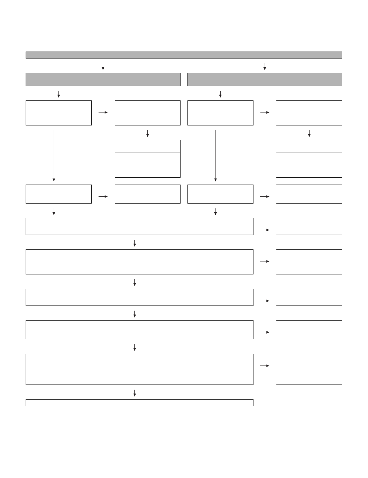
No video (1)
COMPOSITE: No external input video
[INPUT-1]
Is INPUT-1 selected on the
input select menu screen? Is
the INPUT-SELECT for the
input signal?
YES YES
Is there the COMPOSITE
video signal input at pin (71)
of IC501 (AV_SWITCH)?
YES YES
Is there the COMPOSITE video signal output at pin (60) of IC501? NO Check IC501 and its periph-
Is there the COMPOSITE video signal output at pin (2) of connector (SC501) on the TERMINAL unit? NO Check the line between
NO Select INPUT-1 on the input
select menu screen for the
right input signal.
Does the INPUT-1 V2.PLUG
detection function?
Check the line between pin
(6) of input terminal (J508)
and pin (76) of IC501
(AV_SWITCH).
NO Check the line between pin
(7) of J508 and pin (71) of
IC501.
YES
Is INPUT-2 selected on the
input select menu screen?
Is there the COMPOSITE
video signal input at pin (3)
of IC501 (AV_SWITCH)?
COMPOSITE: No external input video
[INPUT-2]
NO Select INPUT-2 on the input
select menu screen.
Does the INPUT-2 V3.PLUG
detection function?
Check the line between pin
(6) of input terminal (J509)
and pin (2) of IC501
(AV_SWITCH).
NO Check the line between pin
(7) of J509 and pin (3) of
IC501.
eral circuits.
IC501 and SC501 (Q501,
Q502 and IC503 peripheral
circuits, etc.).
YES
Is there the COMPOSITE video signal input at pin (2) of connector (SC2202) on the MAIN unit? NO Check the SC501 and
SC2202 connectors.
YES
Is there the COMPOSITE video signal input at pin (AN16) of IC8001 (CPU)? NO Check the line between
SC2202 and IC8001
(Q2212, etc.).
YES
Are the LVDS signal outputs at the LVDS 1st channel and 2nd channel of IC8001?
LVDS_TX_0_DATA0_P/N(C7/B7), LVDS_TX_0_DATA1_P/N(E7/D7), LVDS_TX_0_DATA2_P/N(C6/B6),
LVDS_TX_0_DATA3_P/N(C5/B5), LVDS_TX_0_DATA4_P/N(E5/D5), LVDS_TX_0_CLK_P/N(E6/D6),
LVDS_TX_1_DATA0_P/N(B4/A4), LVDS_TX_1_DATA1_P/N(E4/D4), LVDS_TX_1_DATA2_P/N(B3/A3),
LVDS_TX_1_DATA3_P/N(B1/B2), LVDS_TX_1_DATA4_P/N(F5/F6), LVDS_TX_1_CLK_P/N(C2/C3).
YES
Check the panel module.
NO Check IC8001 and its
peripheral circuits (IC8151
thru IC8154, etc.).
3 – 1
Page 29
No video (2)
LC-32/37D62U SUPPLEMENT 1st
COMPONENT: No external input video
Is INPUT-1 selected on the input select menu screen? Is the INPUTSELECT for the input signal?
Select INPUT-1 on the input select menu screen for the
right input signal.
Does the INPUT-1 C2.PLUG detection function? Does the INPUT-3 C1.PLUG detection function?
Check the line between pin (6) of input terminal (J502) and
pin (40) of IC501 (AV_SWITCH).
YES
Is there the COMPONENT video signal input at pins (27) (Y) / (29) (Pb)
and (31) (Pr) of IC501 (AV_SWITCH)?
Check the line between the input terminals of J502 and
IC501.
YES
Is there the COMPONENT video signal output at pins (60) (Y) / (59) (Pb) and (58) (Pr) of IC501?
[COMPOSITE signal input] Is there the COMPONENT video signal output at pins (2), (4) and (6) of connector (SC501) on the TERMINAL unit?
Are there the COMPONENT video signal inputs at pins(2),(4) and (6) of
connector(SC2202) on the MAIN unit?
[INPUT-1]
YES
YES
Is INPUT-3 selected on the input select menu screen? Is the INPUTSELECT for the input signal?
NO
YES
Is there the COMPONENT video signal input at pins (21) (Y) / (23) (Pb)
and (25) (Pr) of IC501 (AV_SWITCH)?
NO
YES
Check IC501 and its peripheral circuits.
NO Check the line between IC501 and SC501 (Q501 thru
NO Check the line between SC501 and SC2202 connectors.
COMPONENT: No external input video
Select INPUT-3 on the input select menu screen for the
right input signal.
Check the line between pin (6) of input terminal (J507) and
pin (38) of IC501 (AV_SWITCH).
Check the line between the input terminals of J507 and
IC501.
Q504, etc.).
[INPUT-3]
NO
NO
NO
YES
Is there the COMPONENT video signal input at pin(16) of IC3201(SYNC)?
NO
Check the line between SC2202 and IC3201 (Q2210, etc.).
[Format: 480i]
Are there the COMPONENT video signal inputs at pins(AM21)(Y)/
(AN21)(Pb) and (AL21)(Pr) of IC8001(CPU)?
NO
Check the line between the connector of SC2203 and
IC8001(Q2204, Q2206 and Q2208, etc.).
YES
Are the LVDS signal outputs at the LVDS 1st channel and 2nd channel of IC8001?
LVDS_TX_0_DATA0_P/N(C7/B7), LVDS_TX_0_DATA1_P/N(E7/D7), LVDS_TX_0_DATA2_P/N(C6/B6), LVDS_TX_0_DATA3_P/N(C5/B5),
LVDS_TX_0_DATA4_P/N(E5/D5), LVDS_TX_0_CLK_P/N(E6/D6),
LVDS_TX_1_DATA0_P/N(B4/A4), LVDS_TX_1_DATA1_P/N(E4/D4), LVDS_TX_1_DATA2_P/N(B3/A3), LVDS_TX_1_DATA3_P/N(B1/B2),
LVDS_TX_1_DATA4_P/N(F5/F6), LVDS_TX_1_CLK_P/N(C2/C3).
YES NO
Check the panel module. Check IC8001 and its peripheral circuits.(IC8151 thru IC8154, etc.)
[Format: 480p/720p/1080i/1080p]
Are there the COMPONENT video signal inputs at pins(10)(Y)/(4)(Pb)
and (16)(Pr) of IC3301(ADC)?
NO
Check the line between the connector of SC2202 and
IC3301(Q2211, Q2209 and Q2213, etc.).
YES
[Format: 480p/720p/1080i/1080p]
Are there the HD_DVI[29:0], HD_DVI_CLK_P, HD_DVI_VSYNC,
HD_DVI_HSYNC, HD_DVI_DE signal outputs from IC3301?
NO
Check IC3301 and its peripheral circuits.
YES
[Format: 480p/720p/1080i/1080p]
Are there the HD_DVI[29:0], HD_DVI_CLK_P, HD_DVI_VSYNC,
HD_DVI_HSYNC, HD_DVI_DE signal inputs to IC8001(CPU)?
NO
Check the line between IC3301 and IC8001.
YES
3 – 2
Page 30
LC-32/37D62U SUPPLEMENT 1st
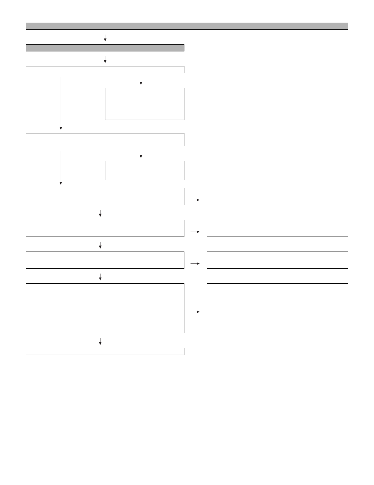
S-VIDEO: No external input video [INPUT-2]
Is INPUT-2 selected on the input select menu screen?
NO
Does the INPUT-2 S3_PLUG
detection function?
Check the line between pin(6) of
input terminal(J503) and pin(42)
of IC501(AV_SW).
YES
Are there the S-VIDEO signal inputs at pins(5)(Y) and (7)(C) of
IC501(AV_SW)?
NO
Check the line between
pins(3)(Y)/(4)(C) of J503 and
pins(5)/(7) of IC501.
YES
Are there the S-VIDEO signal outputs at pins(2)(Y) and (4)(C) of connector(SC501) on the TERMINAL unit?
No video (3)
NO Check the line between IC501 and SC501 (Q501 thru Q504,
IC503 and peripheral circuit, etc.).
YES
Are there the S-VIDEO signal inputs at pins(2)(Y) and (4)(C) of connector(SC2202) on the MAIN unit?
YES
Are there the S-VIDEO signal inputs at pins(AL17)(Y) and (AL16)(C) of
IC8001(CPU)?
YES
Are the LVDS signal outputs at the LVDS 1st channel and 2nd channel
of IC8001?
LVDS_TX_0_DATA0_P/N(C7/B7), LVDS_TX_0_DATA1_P/N(E7/D7),
LVDS_TX_0_DATA2_P/N(C6/B6), LVDS_TX_0_DATA3_P/N(C5/B5),
LVDS_TX_0_DATA4_P/N(E5/D5), LVDS_TX_0_CLK_P/N(E6/D6),
LVDS_TX_1_DATA0_P/N(B4/A4), LVDS_TX_1_DATA1_P/N(E4/D4),
LVDS_TX_1_DATA2_P/N(B3/A3), LVDS_TX_1_DATA3_P/N(B1/B2),
LVDS_TX_1_DATA4_P/N(F5/F6), LVDS_TX_1_CLK_P/N(C2/C3).
YES
Check the panel module.
NO Check the line between SC501 and SC2202 connectors.
NO Check the line between SC2203 and IC8001 (Q2205 and
Q2207, etc.).
Check IC8001 and its peripheral circuits.(IC8151 thru IC8154,
etc.)
NO
3 – 3
Page 31

No video at UHF/VHF broadcast signal reception No video at digital broadcast signal reception
Is the specified TV signal selected on the input select menu screen?
LC-32/37D62U SUPPLEMENT 1st
No video (4)
Is there the analog video
signal output at the output
pin (13) of tuner (TU2201)?
YES
Is there the CVBS3 signal
input at pin (AM19) of
IC8001 (CPU)?
YES
Are the LVDS signal outputs at the LVDS 1st channel and 2nd channel of IC8001?
LVDS_TX_0_DATA0_P/N(C7/B7), LVDS_TX_0_DATA1_P/N(E7/D7), LVDS_TX_0_DATA2_P/N(C6/B6), LVDS_TX_0_DATA3_P/N(C5/B5),
LVDS_TX_0_DATA4_P/N(E5/D5), LVDS_TX_0_CLK_P/N(E6/D6), LVDS_TX_1_DATA0_P/N(B4/A4), LVDS_TX_1_DATA1_P/N(E4/D4),
LVDS_TX_1_DATA2_P/N(B3/A3), LVDS_TX_1_DATA3_P/N(B1/B2), LVDS_TX_1_DATA4_P/N(F5/F6), LVDS_TX_1_CLK_P/N(C2/C3).
Check the panel module. Check IC8001 and its peripheral circuits (IC8151 thru IC8154, etc.).
NO Check the tuner and their
peripheral circuits
(TUN_SDA/SCL).
NO Check the line between
TU2201 and IC8001
(Q2214, etc.).
YES NO
Is there the video signal output at the output pins (19)
and (20) of tuner (TU2201)?
YES
NO Check the line between pins
(AM33/AM34) of IC8001
and pins (19/20) of
TU2201(L2205, C2255 and
C2263, etc.)
3 – 4
Page 32

LC-32/37D62U SUPPLEMENT 1st
Select INPUT-4 on the input select menu screen for the
right input signal.
Does the HOT PLUG detection function?
Does the HDMI_DDC_5VPOW_IN1 signal come from
pin (18) of connector (SC1601) to pin (32) of IC1604
(HDMI_SW)?
Does the signal come from pin (16) of IC1604 to pin
(19) of SC1601?
YES
[HDMI signal input] No video (5)
No external input video [INPUT-4]
Is INPUT-4 selected on the input select menu screen?
NO
NO
NO
YES
NO Check the line between IC1604 and SC1601 (IC1608,
Check the line between SC1601 and IC1604 (R1727,
etc.).
Q1605 and Q1602, etc.).
Does the signal come from connector (SC1601) to the input pins (18 and
19) (CLK±), (21 and 22) (D0±), (24 and 25) (D1±), and (27 and 28) (D2±),
all of IC1604?
YES
Does the signal come from pins (10 and 11) (CLK±), (7 and 8) (D0±), (4
and 5) (D1±), and (1 and 2) (D2±) of IC1604 to pins (57 and 58), (61 and
62), (65 and 66), and (69 and 70) of IC1502?
YES
Are there the U3VINY [7:0], U3VINR [7:0], U3VINPBPR [7:0], U3VDIN,
U3HDIN, U3DEIN and U3VINCLK signal outputs from IC1510?
YES
Are there the HD_DVI [29:0], HD_DVI_CLK, HD_DVI_DE,
HD_DVI_VSYNC and HD_DVI_HSYNC signal inputs at IC8001 (CPU)?
YES
Are the LVDS signal outputs at the LVDS 1st channel and 2nd channel of
IC8001?
LVDS_TX_0_DATA0_P/N(C7/B7), LVDS_TX_0_DATA1_P/N(E7/D7),
LVDS_TX_0_DATA2_P/N(C6/B6), LVDS_TX_0_DATA3_P/N(C5/B5),
LVDS_TX_0_DATA4_P/N(E5/D5), LVDS_TX_0_CLK_P/N(E6/D6),
LVDS_TX_1_DATA0_P/N(B4/A4), LVDS_TX_1_DATA1_P/N(E4/D4),
LVDS_TX_1_DATA2_P/N(B3/A3), LVDS_TX_1_DATA3_P/N(B1/B2),
LVDS_TX_1_DATA4_P/N(F5/F6), LVDS_TX_1_CLK_P/N(C2/C3).
NO
NO
NO Check IC1510 and its peripheral circuits.
NO Check the line between IC1502 and IC1604.
NO
Is IC1601 (EEPROM) accessed by I2C, with HDMI connected, to read the DDC_I2C CLOCK/DATA data?
NO
Check the DDC line and its peripheral circuits (IC1601
(EEPROM) and its peripherals).
Check IC1502, IC1604 and their peripheral circuits.
Check IC8001 and its peripheral circuits (IC8151 thru
IC8154, etc.).
Check the panel module.
YES
3 – 5
Page 33

[HDMI signal input] No video (5)
No external input video [INPUT-5]
Is INPUT-5 selected on the input select menu screen?
NO
Select INPUT-5 on the input select menu screen for the
right input signal.
NO
Does the HOT PLUG detection function?
Does the HDMI_DDC_5VPOW_IN2 signal come from pin
(18) of connector (SC1602) to pin (52) of IC1604
(HDMI_SW)?
YES
Does the signal come from pin (36) of IC1604 to pin (19)
of SC1602?
YES
Does the signal come from connector (SC1602) to the input pins (38
and 39) (CLK±), (41 and 42) (D0±), (44 and 45) (D1±), and (47 and 48)
(D2±), all of IC1507?
LC-32/37D62U SUPPLEMENT 1st
NO
NO Check the line between IC1604 and SC1602 (IC1609,
NO
Check the line between SC1602 and IC1604 (Q1505,
Q1507, etc.).
Q1606, Q1603).
Is IC1603 (EEPROM) accessed by I2C, with HDMI connected, to read the DDC_I2C CLOCK/DATA data?
YES
Does the signal come from pins (10 and 11) (CLK±), (7 and 8) (D0±), (4
and 5) (D1±), and (1 and 2) (D2±) of IC1604 to pins (57 and 58), (61
and 62), (65 and 66), and (69 and 70) of IC1502?
YES
Are there the U3VINY [7:0], U3VINR [7:0], U3VINPBPR [7:0], U3VDIN,
U3HDIN, U3DEIN and U3VINCLK signal outputs from IC1510?
YES
Are there the HD_DVI [29:0], HD_DVI_CLK, HD_DVI_DE,
HD_DVI_VSYNC and HD_DVI_HSYNC signal inputs at IC8001
(CPU)?
YES
Are the LVDS signal outputs at the LVDS 1st channel and 2nd channel
of IC8001?
LVDS_TX_0_DATA0_P/N(C7/B7), LVDS_TX_0_DATA1_P/N(E7/D7),
LVDS_TX_0_DATA2_P/N(C6/B6), LVDS_TX_0_DATA3_P/N(C5/B5),
LVDS_TX_0_DATA4_P/N(E5/D5), LVDS_TX_0_CLK_P/N(E6/D6),
LVDS_TX_1_DATA0_P/N(B4/A4), LVDS_TX_1_DATA1_P/N(E4/D4),
LVDS_TX_1_DATA2_P/N(B3/A3), LVDS_TX_1_DATA3_P/N(B1/B2),
LVDS_TX_1_DATA4_P/N(F5/F6), LVDS_TX_1_CLK_P/N(C2/C3).
NO
Check the DDC line and its peripheral circuits (IC1603
(EEPROM) and its peripherals).
NO
NO Check IC1510 and its peripheral circuits.
NO
NO
Check IC1502, IC1604 and their peripheral circuits.
Check the line between IC1502 and IC1604.
Check IC8001 and its peripheral circuits (IC8151 thru
IC8154, etc.).
Check the panel module.
YES
3 – 6
Page 34

LC-32/37D62U SUPPLEMENT 1st
No audio (1)
[Audio signal] INPUT-1 No audio [Audio signal] INPUT-2 No audio [Audio signal] INPUT-3 No audio
[INPUT-1 input]
Is INPUT-1 selected on the input select
menu screen?
NO
Is the audio output selected
for “VARIABLE” on the menu
screen?
YES
Set the audio output to
“FIXED”.
YES
[INPUT-1] Does the audio signal come
from pins (4) (L) and (2) (R) of input terminal (J508) to pins (8) (L) and (6) (R) of
connector (SC502) on the TERMINAL
unit?
NO
Check the audio signal from
J508 to SC502, and their
peripheral circuits.
YES
[INPUT-1] Is there the audio signal input at
pins (8) (L) and (6) (R) of connector
(SC2201) on the MAIN unit?
NO
Check the SC502 and
SC2201 connectors.
YES
[INPUT-1] Does the audio signal come
from pins (8) and (6) of SC2201 to pins
(35) (L) and (36) (R) of IC1403 (CODEC)?
[INPUT-2 input]
Is INPUT-2 selected on the input select menu
screen?
NO
Is the audio output selected for
“VARIABLE” on the menu
screen?
YES YES
Set the audio output to “FIXED”. Set the audio output to
YES
[INPUT-2] Does the audio signal come from
pins (4) (L) and (2) (R) of input terminal (J509)
to pins (12) (L) and (10) (R) of connector
(SC502) on the TERMINAL unit?
NO
Check the audio signal from J509
to SC502, and their peripheral circuits.
YES
[INPUT-2] Is there the audio signal input at
pins (12) (L) and (10) (R) of connector
(SC2201) on the MAIN unit?
NO
Check the SC502 and SC2201
connectors.
YES
[INPUT-2] Does the audio signal come from
pins (12) (L) and (10) (R) of SC2201 to pins
(37) (L) and (38) (R) of IC1403 (CODEC)?
[INPUT-3 input]
Is INPUT-3 selected on the input select
menu screen?
NO
Is the audio output selected
for “VARIABLE” on the menu
screen?
“FIXED”.
YES
[INPUT-3] Does the audio signal come
from pins (4) (L) and (2) (R) of input terminal (J505) to pins (4) (L) and (2) (R) of
connector (SC502) on the TERMINAL
unit?
NO
Check the audio signal from
J505 to SC502, and their
peripheral circuits.
YES
[INPUT-3] Is there the audio signal input
at pins (4) (L) and (2) (R) of connector
(SC2201) on the MAIN unit?
NO
Check the SC502 and
SC2201 connectors.
YES
[INPUT-3] Does the audio signal come
from pins (4) (L) and (2) (R) of SC2201 to
pins (40) (L) and (41) (R) of IC1403
(CODEC)?
NO
Check the line between
SC2201 and IC1403 and their
peripheral circuits.
YES
Does the audio signal come from pins(4)(COD_LRCK), (5)(COD_BCK) and (6)(COD_SDOUT) of IC1403 to pins(AK24), (AH24) and (AJ24) o
IC8001(CPU)?
YES
Does the audio signal come from pins(AJ25)(DSP_LRCK), (AK25)(DSP_BCKIN),
(AL25)(DSP_SDIN1) and (L32)(DSP_SDIN2) of IC8001 to pins(2), (3), (6) and (5) of
IC1402(SOUND_DSP)?
YES
Does the audio signal come from pins(19)(DSP_SDOUT1) and (21)(DSP_SDOUT3) of IC1402
to pins(11) and (12) of IC1403(CODEC)?
Does the audio signal come from pins(AJ25)(DSP_LRCK), (AK25)(DSP_BCKIN) and
(AL24)(DSP_MCLK) of IC8001 to pins(8), (9) and (10) of IC1403?
YES
Does the audio signal come from pins(17)(SP_L) and (18)(SP_R) of IC1403 to pins(11)(SP_L)
and (14)(SP_R) of connector(SC2203) on the MAIN unit?
Check the line between SC2201
and IC1403 and their peripheral
circuits.
YES
NO
NO
Check the line between
SC2201 and IC1403 and
their peripheral circuits.
YES
NO
Check the line between IC1403 and
IC8001.
Check the line between IC8001 and
NO
IC1402.
NO Check the line between IC1402 and
IC1403.
NO Check the line between IC8001 and
IC1403.
NO Check the line between SC2203 and
IC1403(Q1313, Q1314, etc.).
3 – 7
f
Page 35

LC-32/37D62U SUPPLEMENT 1st
YES
Are there the audio signal inputs at pins(11)(L_CH) and (14)(R_CH) of connector(P2704) on
the TERMINAL unit?
YES
Does the audio signal come from pins(11)(L_CH) and (14)(R_CH) of P2704 to pins(5)(L_CH)
and (3)(R_CH) of IC2701(AMP) on the TERMINAL unit?
YES
Is the audio output from IC2701 as specified? NO Check IC2701 and its peripheral circuits.
YES
Check the connector(P2703), speakers and their peripheral circuits.
NO Check the line between P2704 and
SC2203.
Check the line between P2704 and
NO
IC2701, and their peripheral circuits
(AMP_MUTE line, etc.).
3 – 8
Page 36

LC-32/37D62U SUPPLEMENT 1st
No audio (2)
[HDMI analog audio input] INPUT-5 No audio.
Is INPUT-5 selected on the input select menu screen?
NO
Is the audio output selected for “VARIABLE” on the menu screen?
Set the audio output to “FIXED”.
Is the HDMI audio output selected for “Digital” on the menu screen?
Set the HDMI audio output to “Analog”.
YES
Does the audio signal come from pins(4)(L) and (2)(R) of input terminal(J1601) to pins(43)(L) and (44)(R) of IC1403(CODEC) on the MAIN unit?
NO
YES
Does the audio signal come from pins(4)(COD_LRCK), (5)(COD_BCK) and (6)(COD_SDOUT) of IC1403 to pins(AK24), (AH24) and (AJ24) of
IC8001(CPU)?
Check the line between J1601 and IC1403, and their peripheral circuits.
YES
Does the audio signal come from pins(AJ25)(DSP_LRCK), (AK25)(DSP_BCKIN),
(AL25)(DSP_SDIN1) and (L32)(DSP_SDIN2) of IC8001 to pins(2), (3), (6) and (5) of
IC1402(SOUND_DSP)?
YES
Does the audio signal come from pins(19)(DSP_SDOUT1) and (21)(DSP_SDOUT3) of IC1402
to pins(11) and (12) of IC1403(CODEC)?
Does the audio signal come from pins(AJ25)(DSP_LRCK), (AK25)(DSP_BCKIN) and
(AL24)(DSP_MCLK) of IC8001 to pins(8), (9) and (10) of IC1403?
YES
Does the audio signal come from pins(17)(SP_L) and (18)(SP_R) of IC1403 to pins(11)(SP_L)
and (14)(SP_R) of connector(SC2203) on the MAIN unit?
YES
Are there the audio signal inputs at pins(11)(L_CH) and (14)(R_CH) of connector(P2704) on
the TERMINAL unit?
YES
Does the audio signal come from pins(11)(L_CH) and (14)(R_CH) of P2704 to pins(5)(L_CH)
and (3)(R_CH) of IC2701(AMP) on the TERMINAL unit?
NO
Check the line between IC1403 and
IC8001.
NO
NO Check the line between IC1402 and
NO Check the line between IC8001 and
NO Check the line between SC2203 and
NO Check the line between P2704 and
NO
Check the line between IC8001 and
IC1402.
IC1403.
IC1403.
IC1403(Q1313, Q1314, etc.).
SC2203.
Check the line between P2704 and
IC2701, and their peripheral circuits
(AMP_MUTE line, etc.).
YES
Is the audio output from IC2701 as specified? NO Check IC2701 and its peripheral cir-
cuits.
YES
Check the connector(P2703), speakers and their peripheral circuits.
3 – 9
Page 37

LC-32/37D62U SUPPLEMENT 1st
No audio (3)
No audio at UHF/VHF broadcast signal reception. No audio at digital broadcast signal reception.
Is TV selected on the input select menu screen? Is TV selected on the input select menu screen?
NO
Is the audio output selected for “VARIABLE” on the
menu screen?
Set the audio output to “FIXED”. Set the audio output to “FIXED”.
YES
Is there the SIF signal output at pin(15) of tuner(TU2201) on the
MAIN unit?
NO
Check the tuner(TU2201) and its peripheral circuits. Check the tuner(TU2201) and its peripheral circuits.
YES
Does the SIF signal come from pin(15) of TU2201 to pin(AN23) of
IC8001(CPU)?
NO
Check the line between IC8001 and TU2201 (Q2201,
Q2202, etc.).
YES
Does the audio signal come from pins(AJ25)(DSP_LRCK), (AK25)(DSP_BCKIN), (AL25)(DSP_SDIN1) and (L32)(DSP_SDIN2) of IC8001 to
pins(2), (3), (6) and (5) of IC1402(SOUND_DSP)?
YES
Does the audio signal come from pins(19)(DSP_SDOUT1) and
(21)(DSP_SDOUT3) of IC1402 to pins(11) and (12) of IC1403(CODEC)?
Are there the video signal outputs (IF_OUT_P/N) at the pins(19)
and (20) of tuner(TU2201) on the MAIN unit?
Are there the video signal inputs at pin(AM33) and (AM34) of
IC8001(CPU)?
Check the line between IC8001 and IC1402.
NO Check the line between IC1402 and IC1403.
Is the audio output selected for “VARIABLE” on the
menu screen?
YES
YES
Check the line between IC8001 and TU2202 (L2205,
C2255, etc.).
YES
NO
NO
NO
NO
Does the audio signal come from pins(AJ25)(DSP_LRCK),
(AK25)(DSP_BCKIN) and (AL24)(DSP_MCLK) of IC8001 to pins(8), (9) and
(10) of IC1403?
YES
Does the audio signal come from pins(17)(SP_L) and (18)(SP_R) of IC1403
to pins(11)(SP_L) and (14)(SP_R) of connector(SC2203) on the MAIN unit?
YES
Are there the audio signal inputs at pins(11)(SP_L) and (14)(SP_R) of con-
nector(P2704) on the TERMINAL unit?
YES
Does the audio signal come from pins(11)(L_CH) and (14)(R_CH) of P2704
to pins(5)(L_CH) and (3)(R_CH) of IC2701(AMP) on the TERMINAL unit?
YES
Is the audio output from IC2701 as specified? NO Check IC2701 and its peripheral circuits.
YES
Check the connector(P2703), speakers and their peripheral circuits.
NO
NO Check the line between SC2203 and IC1403 (Q1313,
NO Check the line between P2704 and SC2203.
NO Check the line between P2704 and IC2701, and their
Check the line between IC8001 and IC1403.
Q1314, etc.).
peripheral circuits (AMP_MUTE line, etc).
3 – 10
Page 38

LC-32/37D62U SUPPLEMENT 1st
INPUT-4 No audio (HDMI connected)
INPUT-5 No audio (HDMI connected)
No audio (4)
[INPUT-4 input]
Is INPUT-4 selected on the input select menu screen?
[INPUT-5 input]
Is INPUT-5 selected on the input select menu screen?
YES
[INPUT-4 input] If no video appears, refer to “No external input video (HDMI) [INPUT-4]”.
[INPUT-5 input] If no video appears, refer to “No external input video (HDMI) [INPUT-5]”.
YES
Is the HDMI_MUTE line as specified? NO Check Q1301, IC1302 and their peripheral
YES
Does the HDMI_SPDIF signal come from pin (78) of IC1502(HDMI-Rx) to pins(AM11)
and (AN11) of IC8001(CPU)?
YES
Does the audio signal come from pins(4)(COD_LRCK), (5)(COD_BCK) and
(6)(COD_SDOUT) of IC1403 to pins(AK24), (AH24) and (AJ24) of IC8001(CPU)?
YES
Does the audio signal come from pins(AJ25)(DSP_LRCK), (AK25)(DSP_BCKIN),
(AL25)(DSP_SDIN1) and (L32)(DSP_SDIN2) of IC8001 to pins(2), (3), (6) and (5) of
IC1402(SOUND_DSP)?
YES
Does the audio signal come from pins(19)(DSP_SDOUT1) and (21)(DSP_SDOUT3) of
IC1402 to pins(11) and (12) of IC1403(CODEC)?
NO
NO Check the line between IC1502 and IC8001,
NO Check the line between IC1403 and IC8001.
NO
NO Check the line between IC1402 and IC1403.
Is the audio output selected for “VARIABLE”
on the menu screen?
Set the audio output to “FIXED”.
circuits.
and their peripheral circuits.
Check the line between IC8001 and IC1402.
Does the audio signal come from pins(AJ25)(DSP_LRCK), (AK25)(DSP_BCKIN) and
(AL24)(DSP_MCLK) of IC8001 to pins(8), (9) and (10) of IC1403?
YES
Does the audio signal come from pins(17)(SP_L) and (18)(SP_R) of IC1403 to
pins(11)(SP_L) and (14)(SP_R) of connector(SC2203) on the MAIN unit?
YES
Are there the audio signal inputs at pins(11)(L_CH) and (14)(R_CH) of connec-
tor(P2704) on the TERMINAL unit?
YES
Does the audio signal come from pins(11)(L_CH) and (14)(R_CH) of P2704 to
pins(5)(L_CH) and (3)(R_CH) of IC2701(AMP) on the TERMINAL unit?
YES
Is the audio output from IC2701 as specified? NO Check IC2701 and its peripheral circuits.
YES
Check the connector(P2703), speakers and their peripheral circuits.
NO Check the line between IC8001 and IC1403.
NO Check the line between SC2203 and
IC1403(Q1313, Q1314, etc.).
NO Check the line between P2704 and SC2203.
NO
Check the line between P2704 and IC2701,
and their peripheral circuits (AMP_MUTE line,
etc.).
3 – 11
Page 39

LC-32/37D62U SUPPLEMENT 1st
No audio signal at Digital Audio Output terminal (Analog sound heard)
No INPUT-4/5(HDMI) audio No audio at digital broadcast signal reception
If no video appears, refer to “No external input video (HDMI)
[INPUT-4/5]”.
Is the HDMI_MUTE line as specified? Check the tuner(TU2201) and its peripheral circuits.
NO
Check Q1301, IC1302 and their peripheral circuits. Are there the video signal inputs at pins(AM33) and (AM34) of
YES
Does the HDMI_SPDIF signal come from pin (78) of
IC1502(HDMI-Rx) to pins(AM11) and (AN11) of IC8001(CPU)?
NO
Check the line between IC1502 and IC8001, and
their peripheral circuits.
YES
Is there the SPDIF signal (OPT_OUT) output at pin(AP11) of IC8001(CPU)?
YES
Is there the SPDIF signal (OPT_OUT) input at pin(2) of
IC1304(SPDIF_BUFF&MUTE)?
YES
Is there the MUTE signal input at pin(1) of IC1304? NO Check the MUTE_A_ALL and ACDET signals, and their peripheral
NO Check the line between IC8001 and IC1304.
Are there the video signal outputs (IF_OUT_P/N) at the pins(19) and
(20) of tuner(TU2201) on the MAIN unit?
NO
YES
IC8001(CPU)?
NO
Check the line between IC8001 and TU2201 (L2205,
C2255, etc.).
YES
NO
Check the IC8001 and its peripheral circuits.
circuits(Q1304, Q1312, D1310, etc.).
YES
Is there the SPDIF signal input at pin(1) of D1306(OPTICAL OUTPUT)?
YES
Check the speakers and their peripheral circuits.
NO Check D1306 and its peripheral circuits.
No optical output under the following conditions as per HDMI requirements.
*Audio contents protected.
*Audio frequency beyond 48kHz.
*Audio bit length beyond 16bits.
3 – 12
Page 40

LC-32/37D62U SUPPLEMENT 1st
No monitor audio
Is the audio output from the monitor set at “VARIABLE” or
“FIXED” on the menu screen?
YES
Are the audio signal outputs at pins (24) (L) and (25) (R) of
IC1403 (CODEC)?
YES
Are the audio signal inputs at pins (3) (L) and (5) (R) of
IC1407 (Adder & Active LPF)?
YES
Are the audio signal outputs at pins (1) (L) and (7) (R) of
IC1407?
YES
Are the audio signal outputs at pins (16) (L) and (14) (R) of
connector (SC2201) on the MAIN unit?
YES
Are the audio signal inputs at pins (16) (L) and (14) (R) of
connector (SC502) on the TERMINAL unit?
NO Check the bus line (SCL0/SDA0) and IC1403. Replace as
required.
NO Check IC1403 and its peripheral circuits. Replace as
required.
NO Check the line between IC1403 and IC1407, and their
peripheral circuits.
NO Check IC1407 and its peripheral circuits. Replace as
required.
NO Check the line between IC1407 and SC2201, and their
peripheral circuits.
NO Check the SC2201 and SC502 connectors.
YES
Check the signal up to the monitor audio output terminal
(J501).
NO Check the MUTE.R line (Q507 thru Q509, etc.).
3 – 13
Page 41

LED flashing timing chart for error notification.
250ms 1sec
1) Power LED (The power LED (Green) which lights during TV reception flashes.)
Error type Power red LED operation (1 cycle) Pins are microprocessor pins.
Lamp failure
Flashes once: Fast
Power failure
Flashes twice
Communication failure with main CPU
Flashes 3 times
H: On
L: Off
H: On
L: Off
H: On
L: Off
LC-32/37D62U SUPPLEMENT 1st
L_FL_ERR (pin 43): L failure. Confirmed after 10 consecutive
matches at 500 ms intervals (detected only when the backlight is on).
Note that after five match counts, the lamp cannot be activated except in the monitoring process. (For the first time,
only the inverter is reset, and error OFF is not activated)
Accumulated counts are cleared to 0 when the corresponding
setting in the process A is made or when the power is turned
on with [CH_DOWN] and [VOL_UP] on the unit down or after
continuous illumination for 3 minutes.
Refer to “Power failure details”.
Refer to “Communication failure details”.
Communication line failure or main CPU communication failure. → Check debug statements for the main CPU.
Vsync
Failure
Flashes 4 times
Monitor temperature failure
Flashes 5 times
2) Power failure details (Power LED flashes twice and OPC LED flashes)
Error type Notification LED operation (1 cycle) Pins are microprocessor pins unless otherwise specified.
PS_ON
DET_10V failure
Flashes once
DET_D3V3 failure
Flashes twice
DET_6V failure
Flashes 3 times
H: On
L: Off
H: On
L: Off
H: On
L: Off
H: On
L: Off
H: On
L: Off
VSYNC (pin 52) failure (uninput). Operation failure.
Detected during operation (interruption).
Detected during operation (interruption).
If the panel temperature is 60°C or more for 15 seconds or
more in a row, CAUTION appears on the OSD of AVC
(flashes in red in the lower right screen).
If the panel temperature is 60°C or more for 25 seconds or
more in a row, error standby is activated.
(MONITOR MAX TEMP on page 23 of process A: Change of
temperature failure AD value): Thermistor
DET_10V (pin 57). UR10V or A9V is not applied.
If error is detected during operation, the power is turned on
again by interrupt handling (instantaneous blackout processing).
DET_D3V3 (pin 59) failure (L). D3.3V is not applied.
If error is detected during operation, error standby is activated
by polling.
DET_6V (pin 56) failure (L). D5V or A5V is not applied.
If error is detected during operation, error standby is activated
by polling.
PNL_12V failure
Flashes 5 times
Main failure
Flashes 7 times
H: On
L: Off
H: On
L: Off
DET_PNL_12V (pin 58) failure (L). Panel power is not
applied.
If error is detected during operation, error standby is activated
by polling.
Main microprocessor detection error.
The details are displayed in “ERROR STANDBY CAUSE” on
page 1 of process A for the main microprocessor.
3 – 14
Page 42

LC-32/37D62U SUPPLEMENT 1st
3) Communication failure details (Power LED flashes 3 times and OPC LED flashes)
Error type Notification LED operation (1 cycle)
Initial communication
reception failure
Flashes once
H: On
L: Off
Initial communication from the main CPU is not received.
(After canceling the reset, request for the monitor model No.
is not received.)
Communication line failure or main CPU start-up failure.
Basically, communication logs are analyzed by a bus
monitor or debug print logs are analyzed.
Time-out setting reception failure
Start-up confirmation reception failure
Flashes twice
Regular communication failure
Flashes 3 times
H: On
L: Off
H: On
L: Off
Time-out setting and start-up mode change cannot be
received from the main CPU. (Start-up communication until
time-out setting and start-up mode change is not received.)
Main CPU start-up failure or monitor microprocessor’s reception failure.
Regular communication that is performed at 1 second intervals in the normal operation is interrupted.
Main CPU operation failure or monitor microprocessor’s
reception failure.
3 – 15
Page 43

LC-32/37D62U SUPPLEMENT 1st
LC-32/37D62U SUPPLEMENT 1st
CHAPTER 4. MAJOR IC INFORMATIONS
Service Manual
[1] MAJOR IC INFORMATIONS
1. IC3201 (VHiTB1305FG-1Q)
The TB1305FG has function sync separation and H/V format detector for TV component video signals. (INPUT1/3 and INPUT7)
This IC is controlled by I2C Bus interface.
2. IC3301 (VHiTHC7981+-1Q)
The THC7981 is 10bit A/D Converter for analog video signal.
(Component: INPUT1 and 3, analog RGB: INPUT7)
This IC is controlled by I2C Bus interface and corresponds from 10 to 170MSPS for Full spec HD-TV.
3. IC501 (VHiMM3151XQ-1Q)
This I2C bus-controlled video switch is designed to switch between two-system color difference (component) signal, one-system S video signal and
three-system composite signal.
The analog video signal from the INPUT-1 or INPUT-2 and INPUT-3 input terminal is fed into this IC for selection.
The video output signal from this IC flows through a low-pass filter into the video signal processing circuit IC8001 (iXC138WJQZ).
4. IC2701 (VHiTPA3100D-1Y)
This IC provides for 2-channel A/D and 4-channel D/A (192-kHz sampling).
The analog audio signal from IC501 or INPUT-6 (HDMI-analog audio) or INPUT-7 input terminal is fed into this IC for selection.
The selected signal flows through A/D-unit into the video signal processing circuit IC8001 (iXC138WJQZ).
The digital audio signal (I2S) from IC1402 flows into audio power amplifier IC2701 and AUDIO OUTPUT terminal via each D/A-unit.
5. IC8001 (RH-iXC138WJQZQ)
This LSI is FULL HIGH-DEFINITION 1080p DIGITAL TV SYSTEM-ON-A-CHIP. It combines a cable/terrestrial 4/1024-QAM and 8/16-VSB receiver, a
transport processor, a digital audio processor, a high definition (HD) MPEG video decoder, 2D graphics processing, digital processing of analog video
and audio, analog video digitizer and DAC functions, stereo high-fidelity audio DACs, a 330-MHz millions of instructions per second (MIPS) processor, and a peripheral control unit providing a variety of television control functions.
The cable/terrestrial receiver directly samples a tuner output with an analog-to-digital (ADC) converter. The LSI digitally resamples and demodulates
the signal with recovered clock and carrier timing, filters and equalizes the data, and passes soft decisions to an ATSC A/53 and ITU-T J.83 Annex A/
B/C-compatible decoder. It has an MPEG-2 Digital Video Broadcasting (DVB)-compliant transport processor with advanced section filtering capability,
DVB descrambler, and an MPEG-2 (MP@HL profile) video decoder.
Audio support includes a BTSC and a Dolby AC3/MPEG-2 Layer 1, 2, audio decoder. The LSI provides analog and digital audio/video outputs. A
SPDIF output and a pair of analog outputs (L-R) are provided via the integrated audio DACs. The NTSC analog video decoder is supported by its own
motion adaptive deinterlacing and 3D comb filtering, including 1080i deinterlacing.
The LSI includes advanced 2D graphics processing. Two transport stream inputs are included. The LSI incorporates a complete MIPS32(r)-based
microprocessor subsystem including caches with bridging to memory and a local bus, where external peripherals can be attached. Integrated peripherals include two USB 2.0, three UARTs, counter/timers and GPIO controllers.
6. IC1502 (VHiSii9125+-1Q)
The Sii9125 supports the HDMI v1.3 specification and allows receipt of 10/12-bit color depth up to 1080p resolutions.
A single Sii9125 provides two HDMI input ports.
This IC decodes TMDS signal to Digital Video signal.
Compatible with the HDCP system, encrypted signals can also be received.
This IC responds to the INPUT-4, 5, 6 HDMI (High-Definition Multimedia Interface) selected by IC1604.
7. IC1604 (VHiSii9185+-1Q)
The Sii9185 is the TMDS Switch devices supporting Revision 1.3 of the HDMI Specification.
This IC is used to select a single set of HDMI/DVI signals from one of three HDMI/DVI receiver-ports, and to generate a fully compliant HDMI/DVI
stream as an output.
It also provides DDC/HDCP, HPD, and +5V switching to allow full compliance to the HDMI/DVI Specification.
On this IC, the INPUT-4, 5, 6 HDMI port are switched.
4 – 1
Page 44

LC-32/37D62U SUPPLEMENT 1st
8. IC803 (VHiSii9181+-1Q)
The Sii9181 is TMDS Switch devices supporting Revision 1.3 of the HDMI Specification.
It is a single HDMI input, single output device used to buffer the TMDS signal.
The Sii9181 is used to receive a set of HDMI/DVI signals from the HDMI/DVI receiver-port, and to generate a HDMI/DVI fully compliant stream as an
output.
It also provides DDC/HDCP, HPD, and +5V switching to allow full compliance to the HDMI/DVI Specification.
On this IC, the INPUT-4 HDMI port is switched.
9. IC2002 (RH-iXB986WJN7Q)
The monitor microprocessor is intended to communicate with the main microprocessor and to operate the system. It also controls power of the entire
system.
10. IC8452 (RH-iXC274WJQZQ)
The 64-Mbit page mode flash memory device stores the main CPU program.
4 – 2
Page 45

MEMO
LC-32/37D62U SUPPLEMENT 1st
4 – 3
Page 46

LC-32/37D62U SUPPLEMENT 1st
Main Unit
E230
HDMI 1
ƂMAƃ 䇼 FC䇽 䇼SA䇽
䇼PD䇽
䇼PH䇽
䇼LB䇽
䇼LV䇽
䇼㪣㪧䇽
䇼䇽
䇼䇽
䇼RA䇽
䇼RA䇽
䇼KM䇽
䇼SP䇽
32" LCD Pane
1920×1080
㪨㪚㪥㪮㪄㪜㪉㪍㪍㪮㪡㪨㪱
㩷㪨㪚㪥㪮㪄㪝㪌㪐㪐㪮㪡㪨㪱
㩷
㪨㪚㪥㪮㪄㪝㪊㪋㪈㪮㪡㪨㪱
㩷
㪨㪚㪥㪮㪄㪜㪉㪌㪏㪮㪡㪨㪱
㩷
㪨㪚㪥㪮㪄㪜㪐㪇㪉㪮㪡㪨㪱
㩷
㪨㪚㪥㪮㪄㪝㪉㪌㪇㪮㪡㪨㪱
Terminal Unit
D999
HDMI 2
㩷
1 㵘23
113
LED Unit D909
KEY Unit D910
㩷
1 㵘23
㩷
1 㵘23
㩷
1 㵘23
㩷
1 㵘23
㩷
1 㵘23
1
12
1
4
41
1
20
1
113
14
Component
Audio L/R
Video + L/R
S-Video
Audio L/R
BROADCOM
IC8001
䇼KM䇽
Analog
Digital
Tuner
TU1101
1
5
14
14
䇼FD䇽
1
6
HDMI
Audio L/R
RF IN
Optical
Out
㩿㪣㪭㪛㪪㩷㪤㪘㪠㪥㩷㪝㪩㪚㪀
㩷
㪨㪧㪮㪙㪟㪜㪈㪉㪇㪮㪡㪨㪱
㪈
㪏㪇
㪈
㪋㪈㪈
㪉㪇
㪈
㪚㪥㪈
㩿㪣㪭㪛㪪㪀
㩷
㪨㪚㪥㪮㪄㪝㪍㪇㪋㪮㪡㪨㪱
㪜
㪠㪚㫏
㪜㪘㪞㪣㪜㪉
㵘
㪚㪥㪉
㩿㪧㪦㪮㪜㪩㪆㪚㪫㪣㪀
㪚㪥㪊
㪚㪥㪋㪚㪥㪌
USB
Video + L/R
Component
㪪㪚㪐㪉㪇㪉
㽲
㪪㪚㪐㪉㪇㪈
㽵
㩷
㪨㪚㪥㪮㪄㪜㪉㪋㪐㪮㪡㪧㪱
LC-32/37D62U SUPPLEMENT 1st
CHAPTER 5. OVERALL WIRING/BLOCK DIAGRAM
Service Manual
[1] OVERALL WIRING DIAGRAM (LC-32D62U)
H
G
F
E
D
C
B
A
12345678910
5 – 1
Page 47

POWER㵘UNIT
RDENCA203WJQZ
䇼PH䇽
䇼PD䇽
32" LCD Panel
1920×1080
AC Socket (2pin)
12
1
6
1
䇼LB䇽
1
3
䇼LA䇽
4
1
1
2
1
2
1
2
1
2
1
2
1
2
1
2
1
2
1
2
1
2
1
2
INV-2㵘Unit
RUNTKA284WJZZ
䇼㪣㪘䇽
㪏㪇
㪈
㪏㪇
㪉㪇
㪈
㪈
㪎
1
3
INV-1㵘Unit
RUNTKA283WJZZ
㩷
㪨㪚㪥㪮㪄㪝㪋㪇㪍㪮㪡㪨㪱
㪠㪚㫏
㪜㪘㪞㪣㪜㪉
LCD Cont㵘UNIT
CPWBX3709TPXZ
㪚㪥㪉
㩿㪧㪦㪮㪜㪩㪆㪚㪫㪣㪀
㪚㪥㪊
㪚㪥㪋㪚㪥㪌
LC-32/37D62U SUPPLEMENT 1st
10 11 12 13 14 15 16 17 18 19
5 – 2
Page 48

LC-32/37D62U SUPPLEMENT 1st
Main Unit
E230
HDMI 1
ƂMAƃ 䇼FC䇽 䇼SA䇽
䇼PD䇽
䇼PH䇽
䇼LB䇽
䇼LV䇽
䇼㪣㪧䇽
䇼䇽
䇼䇽
䇼RA䇽
䇼RA䇽
䇼KM䇽
䇼SP䇽
37" LCD Pan
1920×1080
㪨㪚㪥㪮㪄㪜㪉㪍㪍㪮㪡㪨㪱
㩷㪨㪚㪥㪮㪄㪜㪏㪐㪋㪮㪡㪨㪱
㩷
㪨㪚㪥㪮㪄㪝㪌㪐㪏㪮㪡㪨㪱
㩷
㪨㪚㪥㪮㪄㪜㪉㪌㪏㪮㪡㪨㪱
㩷
㪨㪚㪥㪮㪄㪜㪐㪇㪉㪮㪡㪨㪱
㩷
㪨㪚㪥㪮㪄㪝㪌㪐㪎㪮㪡㪨㪱
Terminal Unit
D999
HDMI 2
㩷
1 㵘23
113
LED Unit D909
KEY Unit D910
㩷
1 㵘23
㩷
1 㵘23
㩷
1 㵘23
㩷
1 㵘23
㩷
1 㵘23
1
12
1
4
41
1
20
1
113
14
Video + L/R
BROADCOM
IC8001
䇼KM䇽
Analog
Digital
Tuner
TU1101
1
5
14
14
䇼FD䇽
1
6
HDMI
Audio L/R
RF IN
Optical
Out
㩿㪣㪭㪛㪪㩷㪤㪘㪠㪥㩷㪝㪩㪚㪀
㩷
㪨㪧㪮㪙㪟㪜㪈㪉㪇㪮㪡㪨㪱
㪏㪇
㪈
㪋㪈㪈
㪉㪇
㪈
㪚㪥㪈
㩿㪣㪭㪛㪪㪀
㩷
㪨㪚㪥㪮㪄㪝㪌㪐㪍㪮㪡㪨㪱
㪠㪚㫏
㪜㪘㪞㪣㪜㪉
㵘
㪚㪥㪉
㩿㪧㪦㪮㪜㪩㪆㪚㪫㪣㪀
㪚㪥㪊㪚㪥㪋
USB
Video + L/R
㪪㪚㪐㪉㪇㪉
㽲
㪪㪚㪐㪉㪇㪈
㽳
㩷
㪨㪚㪥㪮㪄㪜㪉㪋㪐㪮㪡㪧㪱
Component
Audio L/R
S-Video
Audio L/R
Component
[2] OVERALL WIRING DIAGRAM (LC-37D62U)
H
G
F
E
D
C
B
A
12345678910
5 – 3
Page 49

POWER㵘UNIT
RDENCA203WJQZ
䇼PH䇽
䇼PD䇽
37" LCD Panel
1920×1080
Unit
AC Socket (2pin)
12
1
6
1
䇼LB䇽
4
1
1
2
1
2
1
2
1
2
1
2
1
2
1
2
1
2
1
2
1
2
1
2
INV-2㵘Unit
RUNTKA276WJZZ
䇼㪣㪘䇽
㪏㪇
㪈
㪏㪇
㪋㪈㪈
㪚㪥㪈
㩿㪣㪭㪛㪪㪀
1
3
INV-1㵘Unit
RUNTKA275WJZZ
㩷
㪨㪚㪥㪮㪄㪜㪍㪊㪋㪮㪡㪨㪱
㪠㪚㫏
㪜㪘㪞㪣㪜㪉
LCD Cont
㵘UNIT
CPWBX3520TPZF
㪚㪥㪊㪚㪥㪋
1
3
䇼LA䇽
LC-32/37D62U SUPPLEMENT 1st
10 11 12 13 14 15 16 17 18 19
5 – 4
Page 50

LC-32/37D62U SUPPLEMENT 1st
+%
$%/
&KIKVCN#8FGEQFG/CKP
2416'%6
0A%27A456
+%
%1&'%
#-'3
.QECN$752%+
+(KP
&68+5
&6852&+(
+%A
+%A
4'5'6
7#46#
#)%#(6
4)$KP
*8
*&/+KP
%8$55;2D2T
&KIKVCN+0
&8+#=?
&8+%.&8+*5;0%
&8+85;0%
&8+&'
+%A
/#+0
5+(
52&+(
*&/+A.4
+0
+%
5QWPF&52
8*+0,7;
#68.4
+0
+0
176
176
*&/+
2
126+%#.
176
+%
6/&559
5++
+%
&#%
/(2
+%
(.#5*
/D
%8$5
4:AZ
.4
8
8
#(6
*&/+#WFKQ
+0276
+0
2
*&/+A.4
+%
+1
/
8
#/28
8
+%
866
+%
2
:VCN
/*\
.+0'A.4
52176A.4
&KUENGVG
/WVG
.+0'A/76'
&K
UE
N
GVG
/WVG
#/2A/76'
56#0&$;
0A54'5'6
+P
5GNA
+%
''241/
+0
5++A/76'
*&/+
4:AZ
+%
''241/
+P
8
52
5%
+0
&52A/%.-&52A$.-+0&52A.4%-
126A176
+%
$*(
8A#
8A#
+%
+%
/WVG
+5
#WFKQ1WV
8
:VCN
/*
*2.4
$WU
65
+%
*&/+4:
5++
8
/*\
::VCN
/*\
/*\
+%
6*%
+5
5%
:VCN
/*\
0A&$)A456
6Q456QH
GCEJ+%
+%
5;0%
6$
+%
-*\8
+%
''241/
MDKV
+%
-*\
%QPPGEVQT
*QVGN68
6Q2TQNFKQO
65+0176
+0276
+0276
/CKP;8
/CKP%%D
/CKP%T
*&8&
4(+0
67
#PCNQI
&KIKVCN
6WPGT
&A+(
#)%
8
8DTV
+%
-*\8
+%A
+% -*\8
+% -*\8
+%
4GUGV
65
8.4
8.4
8.4
176
8
4'5'6A176D
4'5'6A176D
%1&A.4%-%1&A$%-
&52A5&+0
%1&A5&176
&52A5&176
(TQO*&/+4Z
5%
75$
#68888.4
/*\
+0276
;2D2T
6'4/+0#.
%8$5
;2D2T
.4
%QORQPGPV
+0276
8.4
8.4
ޣ/#ޤ
5%22+0
㪠㪚㪉㪎㪇㪈
㪘㫌㪻㫀㫆㩷㪘㪤㪧
㪫㪧㪘㪊㪈㪇㪇㪛
䇼㪝㪚䇽
䋺㪪㪚㪉㪉㪇㪉㪆㪪㪚㪌㪇㪈㩿㪉㪊㪧㪠㪥䋩
䇼㪪㪘䇽䋺㪪㪚㪉㪉㪇㪊㪆㪧㪉㪎㪇㪋㩿㪉㪊㪧㪠㪥䋩
5
%8$5
8.4
䇼㪪㪧䇽
㪧㪉㪎㪇㪊
+%
#859+6%*
//:3
68
/CKP
1WV
176
8KFGQ
8KFGQ
8
;2D2T
;2D2T
8
8A#
8KFGQ
+%
;%
8A#
%8$5.4
%8$5.4
%QORQPGPV
58KFGQ
8
㩷㩷㪠㪚㪌㪇㪋
㩷㪭㫀㪻㪼㫆㪄㪪㪮
㩷㩷㪤㪤㪈㪎㪊㪉
㪠㪥㪄㪘
㪦㪬㪫
㪠㪥㪄㪙
8A#
㩷㩷㪠㪚㪌㪇㪊
㩷㪭㫀㪻㪼㫆㪄㪪㪮
㩷㩷㪤㪤㪈㪎㪊㪉
㪠㪥㪄㪘
㪦㪬㪫
㪠㪥㪄㪙
8A#
&%1
&%1
5+(
+%
%QPPGEVQTHQT
UQHVYCTG
YTKVKPI
8
[3] SYSTEM BLOCK DIAGRAM
H
G
F
E
D
C
B
A
12345678910
5 – 5
Page 51

LC-32/37D62U SUPPLEMENT 1st
+%
$%/
&KIKVCN#8FGEQFG/CKP%27
ޣ.8ޤ2
R(2%
219'4
((%
+08'46'4
㪣㪚㪛
㪧㪘㪥㪜㪣
㪈㪐㪉㪇㬍㪈㪇㪏㪇
ޣ2)ޤ
R
㧮㧸
㧸㧯㧰
%106
8
8
2(%
$7㨢
#%
X
&219
25A10
74X
20.219
ޣ2*ޤ21 9'4˴22+0
ޣ.#ޤ
RKP
ޣ.2ޤ
2
RKP
㧔20.X㧕
9CXGNGPIVJ
㧦
㧦
ޣ#%ޤ
R
ޣ.$ޤ
2
RKP
ޣ.$ޤ
RKP
ޣ($ޤ
R
+08'46'4
ޣ.#ޤ
RKP
ޣ.%ޤ
RKP
ޣ.%ޤ
RKP
ޣ(%ޤ
R
˴
((%
㪜㪘㪞㪣㪜㪉
㪜㪘㪞㪣㪜㪉
.8&5176
75$
7#46#
7#46$
+1
%8$55;2D2T
?
4Z&6Z&
-';
ޣ-/ޤ 2R
6JGTOKUVQT
20.8
-';-';56#0&$;219
25A1020.219
$78
8QP
#%A&'6
ޣ4#ޤ 2R
12%A.'&219A.'&A4219A.'&A).'&A;1;#-7
4%
12%
.'&
+%
/%
/QPKVQT/KEQO
7#46
2
$78
(4#/'4.7&6'/2=?15A5'6
˴#8
˴#8
˴&8
˴&8
˴&8
˴&8
˴8.8
˴&8
˴&8
˴GVE
+%
''241/A5%.5&#
+%
''241/
$4.(
&'6A20.8&'6A8&'6A8
+1
+1
+1
#%A&'6
8DTV
+1
6*'4/1
#&
12%
#&
+06
4
%
+1
+%
(.#5*
/D
8
#/28
$CEM7R
˴$78
$78
2/A4'3%$1165
+1
0A54'5'6
+1
ޣ4#ޤ 2R
$78
2
2+0
+%
866
+%
&&4
/D
2
20.8
92
5*+2A'020'.A'0
*2A2.7)
*2
A
2.7)
#&
#(6
+%
)CVG
9*(7
5%
20.A&'6=?
/1&'.A&'6=?
92
+1
ޣ-/ޤ 2R
456A*(.5A%2.&
(.#5A9A%2.&
45A$7(A%06
%08UU
4Z&6Z&
*&/+A%'%A2.)
*&/+A%'%A+0
%'%A+A7%1/
%'%A%-A7%1/
$WU%QPPGEVQT
65
.'&
+%
)CVG
$78
5%
/*\
$78
+%
7#46%
%QPPGEVQT
*QVGN68
6Q2TQNFKQO
65+0176
56$A%27
56$
(TQO%27
41/5'.
+%
4GUGV
$78
65
5%
75$
6Q*&/+
(TQO%27
'44A20.
ޣ2&ޤ21 9'4˴22+0
8
8
/*\
:VCN
UVCPFD[
+08'46'4
/#+0
219'429$
/#+0
㪧㪦㪮㪜㪩
㪠㪥㪧㪬㪫
㪚㪟㪄㪬㫇㪆㪛㫆㫎㫅
㪭㫆㫃㪄㪬㫇㪆㪛㫆㫎㫅
6'4/+0#.29$
㪠㪥㪭㪜㪩㪫㪜㪩㩷㪧㪮㪙 㪠㪥㪭㪜㪩㪫㪜㪩㩷㪧㪮㪙
%QPPGEVQTHQT
YTKVKPI
UQHVYCTG
GOWNCVQT
%QPPGEVQTHQT
/QFGN&KUVKPEVKQP
%QPPGEVQTHQT
%QPPGEVQTHQT
&GDWIIKPI
2CPGN&KUVKPEVKQP
10 11 12 13 14 15 16 17 18 19
5 – 6
Page 52

LC-32/37D62U SUPPLEMENT 1st
MAIN Unit (Side-A)
LC-32/37D62U SUPPLEMENT 1st
CHAPTER 6. PRINTED WIRING BOARD ASSEMBLIES
Service Manual
[1] MAIN Unit
H
G
F
E
D
C
B
A
12345678910
6 – 1
Page 53

LC-32/37D62U SUPPLEMENT 1st
10 11 12 13 14 15 16 17 18 19
6 – 2
Page 54

LC-32/37D62U SUPPLEMENT 1st
MAIN Unit
(Side-A Chip)
SC1751
LUG2209
FDC3
R1757
R1755
Q1752 Q1754
R1756
R1796
R1754
R1795
D1752
R1752
IC1753
C1788
Q1751
Q1753
R1775
R1778
SG1751
SC1752
SG1753
SG1755
SG1757
SG1752
R1792
SG1754 R1782
SG1756 R1781
IC1752
R1769
SG1758
R1770
R1773
R1772
R1771
C1764
C1765
C1766
D1603
R1784
R1786
C1769 C1773
C1763
R1791
Q1605
C1768 C1772
C1675
C1762
R1790
R1785
R1787
IC1608
C1767
R1730
R1612
Q1602
R1603
SG1603
SC1601
SG1609
SG1615
SG1621
SG1604
SG1610
SG1616
R1722
R1727
R1669
R1673
SG1622
D1604
IC1604
D1601
Q1606
R1665
R1666
R1616
R1728
Q1603
R1604
R1688
R1601
SG1601
SC1602
R1670
R1674
R1679
R1681
SG1607
R1606
R1605
C1673
SG1613
C1674
R1672
R1675
R1732
C1677
R1678
R1729
SG1619
SG1602
IC1610
SG1608
SG1614
SG1620
R1686
IC1606
C1653
R3317 R3318
R1685
R1687
R3316 R3330
SG1605
L1610
SG1611
D1618
SG1617
L1611
SG1623
SG1606
L1612
D1617
SG1612
SG1618
L1613
IC3301
SG1624
R3322
Q1604
D1602
R1631
R3236
R3237
C3324
C3323
Q1601
SC1603
C3322
R1625
C1668
C1667
D1621
FB1612
R1706
R1695
R1697
IC1605
R1708
C3305
C3306
C3307
C3308
C3309
C3310
R1707
C1672
FB1608
R1694
D1620
C1670
R1712
R3306
R3307
R3308
R3310
R1696
C1664
R1661
R1717
Q1610
R1691
R1648
FB1610
C1656
R1713
R1654
R1718
C1657
R8094
R8143
R8040
R3312
R3313
TP8078
R8146
R3314
R8058
C3333
R8144
C3319
C3320
C3321
TP8013
TP8014
C3311
C3312
R8145
R8053
TP8012
C8128
R8052
TP8011
TP8075
C8125
R8054
TP8068
C8126
R8056
TP8071
C8127
TP8077
R8046
R3315
C8119
R8045
C8118
TP8057
TP8058
R8044
C8117
TP8056
TP8059
R8047
C8120
R8109
C8147
R8110
C8148
TP8064
TP8065
TP8067
TP8070
R3321
R8072
C8131
TP8069
TP8066
TP8060
R8073
C8132
TP8061
R8074
C8133
IC8001
R8070
C8129
R8071
C8130
R8048
C8121
R8075
R8050
C8123
R8049
C8122
R8051
C8124
R8060
R3332
C8137
R8076
R8092
C8138
R3329
R8061
R8091
C8139
TP8080
R9209
R8902
R8104
C8141
R8904
R8901
R8102
R9037
C8142
R8101
R9036
R8103
TP8081
TP8085
TP8082
TP8086
R8012
TP8084
TP8087
TP8083
TP8088
R1736
R1735
R1734
R1532
R1531
R1529
R1733
R1528
R1518
C1564
R1517
X1501
C1563
IC1502
R1525
C1551
C1553
R1534
FB1506
R1512
R1511
C1541
C1542
R1800
C1518
C1514
R1799
C1511
R1798
L1501
R1797
C1506
C1505
C1508
C1507
C1503
FB1505
C1517
C1509
C1504
C9654
FB1501
C1522
C1510
FB1502
C1756
C1502
C1755
C1501
C1521
R2237
FB1752
IC1754
LUG2206
R2236
C1789
Q1620
D1753
R1726
R1725
Q1619
P2002
P9202
SC9202
L9641
CN8601
C8151
R8228
R8255
R8186
R8215 R8245
R8187
R8268
R8269
IC8152
R8216
R8246
TP8028
R8257
R8188
R8230
TP8044
C8140
TP8001
C8154 C8152
R8139
R8006
R8128
R8126
R8127
R8113
R8125
R8117
R8124
C8155 C8153
R8231
R8151
R8258
C8146
R8189
C8145
R8107
R8152
R8217
R8247
R8108
R8259
R8190
R8232
IC8151
R8153
R8248
R8218
R8260
R8191
R8233
R8183
R8182
R8154
C8196
C8197
R8155
R8156
R8157
R8158
R8159
C8198
C8199
R8185
R8192
R8234
R8261
R8184
R8160
R8002
R8219
R8249
R8106
R8262
R8161
R8193
R8235
C8143
IC8154
C8144
R8162
R8250
R8220
R8105
R819
R82
TP
R8
P2603
R2632
C2610
R2633
R2634
Q2601
Q2602
R9609
C9615
C9608
R9614
R9616
R9617
R9618
IC9603
C8171
C8165
C8173
D9608
C9612
C9625
L9603
C9623
C9616
C8166
C8164
C8172
R2601
R2602
TL2662
R2603
FL2614
R2628
TL2660
TL2659
L2612
L2605
L2610
L2604
P2601
L2609
L2603
L2611
L2608
L2602
L2607
L2601
L2606
FB2608
FB2607
FB2606
FB2605
FB2604
R2620
C2605
FL2613
R8601
C2604
R2618
C2602
IC2601
R2619
R2629
SC8601
FL2615
R2630
R2631
FB2602
P2602
C2601
FB2601
FB2609
R2235
R2234
LUG2205
H
G
F
E
D
C
B
A
12345678910
6 – 3
Page 55

4
631
R3236
R3237
C3324
C3323
Q1601
SC1603
C3322
R1625
C1668
C1667
D1621
FB1612
R1706
R1695
R1697
IC1605
R1708
C3305
C3306
C3307
C3308
C3309
C3310
R1707
C1672
FB1608
R1694
D1620
C1670
R1712
R3306
R3307
R3308
R3310
R1696
C1664
R1661
R1717
Q1610
R1691
R1648
FB1610
C1656
R1713
R1654
R1718
R1632
C1657
R1647
R1709
C1665
R1714
R1649
Q1611
R1689
FB1611
C1658
R1650
R1692
R1710
R1635
C1659
R1655
R1715
R1651
C1666
FB1609
C1660
R1716
Q1612
R1652
R1693
R1690
R1719
R1636
C1661
R1656
R1720
C3219
X3201
R1311
L1609
C1662
IC1304
C3217
C1310
R1333
Q1312
C3218
C1313
R3207
D1306
L1301
C3204
C1312
C1311
IC3201
C3229
C3230
C3210
C3202
L3202
C3205
C3206
C3207
C3203
R2256
J1602
C3228
R1602
R1626
C3201
FB1604
C1649
C1608
R1622
C1616
R1621
C1614
C1610
FB1607
R1611
R1628
LUG2208
C1650
C1601
FB1601
R1613
R2257
R1617
C1604
R1618
J1601
C1605
C1606
R1619
R2219
C1603
C2216
R1615
C2215
C2217
R1614
FB1602
C1602
D9002
R9009
D9003
P9005
R9019
D9004
C8107
C8093
k3
IC8004
C8091
R8147
R8148
C8089
FB8008
VA8002
SC8001
VA8001
FB8009
LUG2204
TH2001
SC2201
C2247
C1463 C1458
L2204
TU2201
C2214
R9003
k2
R9004
C9002
R9040
IC9002
R9041
IC9003
R9007
R9005
C9001
R9039
R9038
R9006
R9001
C8451
R8456
IC8451
C8453
R8457
C8452
R9014
R9015
R9011
R9010
R9013
R9012
C3208
C3209
C8456
C3211
R2276
TP2213
R2273
C2233
R2278
IC8452
R9311
C3212
R2275
R2277
R2266
R2265
C3214
TP2210
TP2212
C3216
R2249
C2240
R2260
C2254
C2252
C2231
C8458
R2274
C2256
R9324
R8099
R8098
R2279
R8015
R8017
R8140
R8083
R8082
C2235
R8095
R2252
R2255
C2242
R8016
L2205
R8069
C2255
TP8049
R8005 R8008
C8136 C8135
C2257
C2258
C2239
X8001
L2206
C2259
C2260
L2207
C2250
R2262
C2261
C2262
L8001
L2208
TP8016
R8011
C2263
R8130
FL8001
R8088
C8134
R8085
R8086
R8087
R8089
C2249
R8003
R8094
R8143
R8040
R3312
R3313
TP8078
R8146
R3314
R8058
C3333
R8144
C3319
C3320
C3321
TP8013
TP8014
C3311
C3312
R8145
R8053
TP8012
C8128
R8052
TP8011
TP8075
C8125
R8054
TP8068
C8126
R8056
TP8071
C8127
TP8077
R8046
R3315
C8119
R8045
C8118
TP8057
TP8058
R8044
C8117
059
R8159
C8198
C8199
R8185
R8192
R8234
R8261
R8184
R8160
R8002
R8219
R8249
R8106
R8262
R8161
R8193
R8235
C8143
IC8154
C8144
R8162
R8250
R8220
R8105
R8194
R8263
TP8041
R8236
R9018
TL8002
TP8030
R8123
TP8010
C8202
C8201
TP8042
TP8043
TP8079
R8035
TP8047
C8200
C8203
R8195
R8237
R8264
R8221
R8253
R8196
R8238
R8265
TP8027
R8025
R8135
D8002
IC8153
R8222
R8254
R8197
R8266
R8239
R9308
C8204
R9301
R9302
R8023
R9309
R9307
IC8502
P9301
R9303 R9304
R9316 R9318
R8502
R8503
IC9301
C9301
Q9301
R9314
R9319
R9305
C8503
C1445
C8504
C1443
C1446
C1444
R1437
C1442
IC1405
P8501
R1438
C1447
R1439
C1448
C8505
R1444 R1442
k1
C1453
R1441
C1457
R2016
R1446
C1455
IC1406
R1447
C1450
IC2008
C1451
C1452
R1443
R1445
C1454
C1449
R1440
C2016
R2049
R2001
R2006
R1448
R2046
C1456
C2026
R2047
C2010
R1433
R1435
C2014
C1438
R2052
R2051
C2015
IC1404
R2042
C1437
C1436
R1434
C1435
D2003
R2041
R1436
R2004
R2077
R2058
C1439
IC2007
R2048
C2013
C2024
R2044
C2020
R1310
SC9201
SC2202
SC2203
FDC4
C2221
LUG2203
FB2207
C2220
R2226
R2225
R2066
IC2004
R2015
R2061 R2060
C2018
C2017
P9001
P2001
tptp4
R2068
R2002
R2029
R2011
R2033
R2032
R2019
Q2001
IC2002
R2023
R2024
Q2007 Q2006
C2012
C2008
R2013
R2076
R2035
R2003
C2002
R2007
IC2001
R2036
R2034
R2026
R2070
R2050
R2071
R2005
P9702
X2002
C2003
C2001
L9602
C8506
R8501
IC8501
C8502
L9601
C8501
D9601
P9701
C9624
C9629
IC9602
C9607
C9604
R9625
R9611
R9612
R9610
R9656
R2254
R2253
C8186
C8174
C8190
LUG2207
C8189
C8175
C8191
P2603
R2632
C2610
R2633
R2634
Q2601
Q2602
LC-32/37D62U SUPPLEMENT 1st
10 11 12 13 14 15 16 17 18 19
6 – 4
Page 56

LC-32/37D62U SUPPLEMENT 1st
MAIN Unit (Side-B)
H
G
F
E
D
C
B
A
12345678910
6 – 5
Page 57

LC-32/37D62U SUPPLEMENT 1st
10 11 12 13 14 15 16 17 18 19
6 – 6
Page 58

LC-32/37D62U SUPPLEMENT 1st
MAIN Unit
(Side-B Chip)
TL2205
TL2207
TL2209
TL2211
TL2213
TL2215
TL2212
TL2206
TL2208
TL2210
TL8007
TL8006
TL8005
C2238
TL8004
TL8034
C2244
TL8036
TL8037
R2296
R2295
C2241
TL8038
TP2214
C2236
R2258
R2248
TL8035
C2218
Q2202
TL9042
R2220R2221
TL9041
Q2201
TL9040
R2214
R2215
R2216
R2212
C2213
TL2201
TL9039
R2211
R2209
TL1602
TL2267
TL2266
TL2265
TL2263
TL2262
TL1603
TL1601
TL1605
TL1610
TL1608
R2271
R2259
R2264
R2286
R3212
Q2210
C3232
R3235
TL1303
R2244
R3209
R3208
C3231
R2267R2263
TL1304
LUG2211
R2285
C3221
Q2209
C3222
TL1302
C3224
R3224
R3233
R2291R2287
R2293
Q2211
R2302
R2303
R3234
R2289R2292
R
TL1
TL2297
R224
R228
R8007
R8010
R8009
Q2205Q2206
TL2292
R2246
R2241R2239
TL9386
R2288
R2242
R2283
TL2296
TL9303
R8018
Q2207Q2204
TL2295
TL9385
R2250R2245R2240
R2233
TL2294
R2282
R8453
TL8457
C2253
R9312
TL2293
R2299
Q2212
R2270R2269
TL9323
R8475
TL8455
C8461
R8474
TL8454
R2305
R2304
IC8454
C8462
C8460
TL8453
TL8456
LUG2212
TL2231
TL2230
TL2202
TL2261
TL2237
TL2235
TL2234
TL2233
C2204C2201
R2205
R2204
R2203
R2281
FB2202
FB2201
R2310
C2206
R2280R2306
R2308
R2309
R2217
Q2214
R2307
C2202
R2222
R2223
C2229
C2228
C2225
C2219
C2230
R2227
C2237
R2232
R2228
R2224
IC2203
R2261
C2234
C2232
R2243
R2229
C2227
C2226
C2223
C2222
C2224
C1462
R1461
R1431
R1453
R1454
R1432
R1459
C1461
R1458
R1460
IC1407
C1464
R1457
C1460
R1456
R1462
C1465
TL2214
TL2216
R1451
R1455
C1459
TL2222
TL2224
TL2226
R1452
TL2218
TL2241
TL2243
TL2245
TL2247
TL2249
TL2251
TL2253
TL2220
TL2239
R2202
TL2223
TL2217
TL2219
TL2221
R2201
TL2246
TL2225
TL2227
TL2238
TL2240
TL2242
TL2244
TL2248
TL2250
TL2252
TL2260
TL2254
TL2256
TL2258
TL2268
TL2270
TL2272
TL2274
TL2276
TL2278
TL2280
TL2282
TL2284
TL2286
TL2288
TL2290
C2212
C2209
C2208
FB2203
FB2204
FB2205
tptp1
TL2255
TL2269
TL2271
TL2273
TL2275
TL2277
TL2279
TL2281
TL2283
TL2285
TL2287
TL2289
TL2259
C2207
TL2257
FB2206
Q1307
Q1313
Q1314
TL9219
TL9210
TL9212
R1318
R1330
R1317
R1329
R1315R1314
TL9209
TL9211
TL9213
C1303
R9201
C9003
R1302
R9205
R9024
R9022
Q9001
IC9001
R1301
TP9001
R1336
R9023
tptp2
R1308
R9002
D1312
R1341
D1304
IC1301
D1314
D1313
D1301
D1307
D1302
R1312
D1309
D1308
R1322
C1421
C1422
R1338
R1309
R1335
Q1309
R1304
R1422
R1425
Q1304
D1310
C1410
C1413
R1337
D1305
R1323
C1440C1441
C1429
C1430
C1314
D1311
R1416
R1418
C1414C1423
R1415
C1415
C1424
R1414
C1426
R1404
C1425
R1405
R1428
C1434
TP2008
TP2004
R1406
TP2015
R1427
C1433
IC1403
R1407
TP2006
R1408
TP2005
C1431
R1429
C1427
R1409
C1428
R1410
R2012
C1432
R1430
TP2001
TP2014
R1411
TP2002
C1406
C1407
TP2003
R1426
C1409
TP2011
TP2013
C1408
R2014
R2072
C1419
TP2007
R1450
R1423
R1413
C1405
TP2009
R1403
R1449
R1412
R9641
C1402
IC1401
IC1402
C1403
C1411
C1412
R1417
C9641
R9645
R1419
R9643
R9644
C9643
R1421
R1420
R1401R1402
C1417
C9645
R9647
C9642
R9646
C1418
X1401
R9642
R9649
C9644
R9648
TL9604
C1401
C1404
C9622
C9621
C9620
D9604
TL8510
TL8511
TL8509
TL8512
R8514
R8515
R8513
R8512
TL9603
TL8504
C9631
TL8503
C9619
TL9351
C9618
TL9302
TL9357
TL9354
TL9348
TL9345
TL9343
TL9340
TL9338
TL9353
TL9381
TL9301
TL9355
TL9349
TL9346
TL9341
TL9380
TL9339
TL9337
TL9378
TL9359
TL9375
TL9350
TL9347
TL9344
TL9342
TL9352
R8509
C8514
X8501
R8508
C8513
TL9379
TL9326
TL9336
TL9328
C8512
TL9331
TL9314
TL9312
C8508
TL8508
R9306
TL9320
C8510
TL9315
TL9310
C8509
TL9311
TL9383
TL9313
C8507
TL9316
R8510
R8511
C8511
TL9382
TL9321
TL9324
TL9384
TL9329
TL9332
TL9335
C8515
TL9317
TL9318
TL8502
TL8505
TL8501
TL8507
TL9319
TL9322
TL9325
TL9327
TL9330
TL9333
TL9334
R8506
TL8506
R8507
C8229
C8178C8176
C8228
C8206
C8205
R8214
C8193
IC8155
R8223
R8224
R8213
C8194
C8195
R8270
C8216
C9721
TL9725
IC9705
TL9710
TL9739
TL9738
C9719
TL9723
TL9737
TL9740
TL9727
R9740
R9741
TL9702
IC9706
TL9741
R9742
C9720
TL9726
R9743
TL9711
TL9742
R9744
C9708
TL9728
TL9720
D9603
D9602
R9702
TL9715
TL9743
R9701
D9606
R9615
TL9736
TL9735
D9644
TL9744
C9613
C9648
D9702
TL9601
R9736R9704
C9709
C9711
TL9701
D9713
Q9641
D9641
Q9701
Q9702
R9705
D9703D9701
TL9729
R9650
TL9724
TL9731
C9647
IC9641
TL9708
TL9722
C9713
C9646
TL9732
TL9717
TL9730
IC9703
TL9716
TL9734
C9718
C9710
TL9733
TL2006
C9005
TL2007
TL9001
TL2008
R9034
TL2009
TL2010
TL9002
TL2011
R9035
TL2012
TL9003
TL2013
TL2014
R1306
TL2001
R2025
TL9005
R1307
IC1302
C1308
R1305
R1303
Q1301
Q1305
R1324
C1301
FDC2
H
G
F
E
D
C
B
A
12345678910
6 – 7
Page 59

LC-32/37D62U SUPPLEMENT 1st
R3235
TL1303
R2244
R3209
R3208
C3231
R2267R2263
TL1304
LUG2211
R2285
C3221
Q2209
C3222
TL1302
C3224
R3224
R3233
R2291R2287
R2293
Q2211
R2302
R2303
R3234
R2289R2292
R2290
R2294
TL1632
Q2213
TP1601
R1711
TL1617
R1644
TL1631
D1616
TL1624
TL1621
R1639
D1615
TL1630
C3303
R1638
TL3302
TL1620
C3304
IC3302
D1623
D1612
R1705
TL1622
C1671
R1701
TL3301
FB3304
TL1623
C3314
C1669
C3337
IC1607
D1622
FB3303
Q3301
R3341
C3336
TL1627
C3313
C3315C3316C3317C3318
TL1612
C1655
R3343
R1700
R3334
TL1626
R3340
R1645
C3332
R3335
C1663
C3331
TL3304
FL3301
Q1608
R3320
C3325
R1646
R1653
R1658
R1657
R1659
R1660
C3335
R3353
C1654
TL1628
C3334
R3327
R3326
C3327
C3328
C3326
R3331
C3302
IC1602
C1651
C3301
C3329
R1609
FB3301
C3330
FB1613
TL1629
FB3302
TL1625
D1606
Q1613
R3342
TL1614
R1623
C1617
C1618
Q1609
TL1613
R1624
R1637
R1641
R1640
R1642
R1643
C1612
TL1615
D1619
IC1603
R1680
R1682
C1611
R1698
D1614
C1636
C1637
FB1605
TL1618
TL1607
C1632
C1633
C1631
C1642
C1648
C1647
C1629
C1628
Q1618
D1607
R1608
C1627
C1626
R1683
C1630
R1667
R1610
R1662
C1625
C1624
R1663
R1684
C1676
R1677
R1676
C1652
IC1609
C1623
C1622
R1731
C1644
C1643
C1646C1639
FB1614
R1521
C1645C1638
C1635
C1634
C1621
C1641
C1640
TP1633
R1520
TL1609
R1668
R1671
C1620
R1607
C1613
R1506
C1619
Q1607
C1615
TL1606
FB1606
R1620
R1627
R1630
R1629
R1633
R1634
C1609
TL1611
D1613
C1607
IC1601
R1664
D1611
FB1603
TL1619
TL1604
TL1616
R1777
R1779
R1780
R1783
D1605
Q1616
TL1758
TL1767
TL1769
C1784
C1785
R1753
R1768
C1787
TL1768
C1786
R1788
TL1755
R1765
R1766
R1794
C1760
C1761
R1758
C1778
C1759
C1758
R1751
C1754
C1782
C1781
Q1756
C1757
C1783
C1771
C1779
C1774C1777
C1780
C1753
FB1753
R1759
C1770
C1775C1776
TL1770
TL1754
R1760
R1762
R1761
R1763
R1764
R1793
R1774
R1776
C1752
TL1756
D1757
IC1751
C1751
TL1753
TL1751
R1767
D1756
FB1751
TL1757
R1789
D1754
Q1757
TL1752
Q1755
FDC1
C2027
C2028
C2029
TL2002
TL2003
TL2004
TL2005
FB2003
FB2004
FB2005
FB2001
R2008
R2009
C2004
C2005
R2010
D9643
C9650
R9655
C9656
C9649
C9653
IC9642
R9651
C9652
TL9641
R9653
R9657
R9654
R9652
C9655
D9642
R2300
C1516C1538C1536C1534C1531C1515
C1530C1528C1526C1524
C1520C1537C1535C1533C1532C1519
C1529C1527C1525C1523
TL1504
C1546
C1543
C1544
C1545
C1540
C1556
FB1508
C1548
C1561
C1559
C1558
TP1501
C1549
C1550
FB1507
C1562
C1557
C1560
C1512
C1513
C1539
C1565
C1567
R1519
C1591
TL1506
C1573
FB1509
C1578
C1577
R1522
C1572
C1574
C1590
C1588C1585C1583C1581
C1570
C1571
TL1505
C1589
C1587C1586C1584C1582
C1575
C1576
C1580
C1579
R1527
R1523
FL1501
R1533
R8020
IC8002
R8019
R3319R3344
R3349
C8086
TL8029
R8004
FB8001
C8075
IC8003
C8079
FB8003
C8014
C8085
C8080
C8082
TL8033
R8001
C8003
R8903
C8087
C8081
C8065
R8137
R8136
C8067
FB8002
C8076
C8064
C8105
C8069
R8038
C8026
C8106
R8039
C8024
C8062
C8016
C8059
C8012
C8032
R8129
C8002
R8100
R8067
C8060
C8066
C8034
R8068
C8061
TP8054
C8040
C8038
C8057
C8030
C8028
C8112
C8007
C8063
C8097
C8027
C8023
R8084
C8036
TP8051
R8042
R8026
C8048
C8098
C8022
C8005
C8033
C8104
C8052
C8006
C8008
C8009
R8142
C8004
TP8002
TP8015
R8066
C8035
C8149
C8010
C8109
C8037
TP8052
R8081
C8039
C8013
C8042
C8096
C8025
C8068
R8077
R8078
C8015
C8103
TP8062
C8094
C8045
C8017
R8080
C8047
TP8063
C8095
R8111
C8102
C8049
C8011
C8051
C8019
C8021
C8020
C8053
R8041
R8063
R8062
C8044
R8090
C8056
C8054
R8138
C8058
C8018
C8050
R8059
R8065
R8131
TP8046
R8064
R8057
C8100
C8115
C8116
C8071
C8043
C8046
C8101
R8122
R8043
C8077
C8099
TP8050
R9315
C8083
TP8025
R9310
C8114
C8090
C8070
TL8074
TP8009
C8088
R8097
C8078
R8141
R8114
R8096
TL8072
R8013
C8072
C8074
C8084
C8073
R9313
R8014
TL8001
C8092
R8120
TL8073
TP8020
R2268
TP8055
TP2211
R8093
R2272
TP8029
TL2291
TP8026
R2238
R8132
R2298
R9317
Q2203Q2208
R8118
R8116
R2311
R2231
R2230
R2297
R2251
TL2297
R2247
R2284
R8007
R8010
R8009
Q2205Q2206
TL2292
R2246
R2241R2239
TL9386
R2288
R2242
R2283
TL2296
TL9303
R8018
Q2207Q2204
TL2295
TL9385
R2250R2245R2240
R2233
TL2294
R2282
TL8457
C8229
C8178C8176
C8228
C8206
C8205
R8214
C8193
IC8155
R8223
R8224
R8213
C8194
C8195
R8270
TL8152
C8184
R8212
C8192
C8185
TL8151
R8271
C8227
C8180C8182
C8179C8177
C8226
R8180
R8211
R8179
R8210
R8178
C8001
R8177
R8209
R8267
R8165
R8176
C8187
C8055
C8188
R8166
R8175
R8164
C8225
C8181
C8183
R8198
C8041
R8199
R8200
R8201
C8031
R8181
R8202
R8163
R8168
R8174
C8224
C8159C8157
R8173
C8029
R8208
R8172
R8171
R8207
R8167
R8170
R8251
R8206
R8169
C8168
C8167
C8223C8222
C8161C8163
C8221
C8156
C8158
R8205
R8204
R8203
C8169
C8170
R8226
R8225
C8218
C8219
C8220
C8160
C8162
LUG2210
R2301
TL8603
TL8601
TL8602
TL8604
R8607
TL8607
TL8606
TL8605
TL8615
TL8617
C9651
R9203
R9206
TL9234
TL9237
TL9238
TL9235
TL9236
TL9240
TL9224
TL9222
TL9208
TL9241
TL9239
TL9223
TL9221
TL9207
TL9201
R9204
R9207
R9208
R9211
TL9275
TL9206
TL9205
TL9204
TL9203
TL9202
R9212R9202
TL2629
TL2632
TL2630
TL2633
TL2631
TL2636
TL2634
TL2637
TL2638
TL2635
TP2603
TP2601
TP2604
TL2648
TP2605
TP2606
TP2602
TL2650
TL2649
TL2623
TL2624
TL2625
R2624
R2625
TL2626
TL2627
R2616
R2626
R2627
R2615
R2622
TL2628
TL2643
TL2603
TL2639
TL2644
TL2640
TL2602
TL2645
TL2651
TL2658
TL2646
TL2642
TL2661
TL2647
TL2641
TL2655
TL2654
TL2657
TL2656
C8217
TL9605
C9614
C8207
R8240
R8227
D9607
C8208
C8209
R8243
C8210
R2637
R2638
R8241
C2608
C8211
C2607
C8212
C2609
R8244
C8213
C8214
R8242
IC2602
TL2619
C8215
TL2652TL2653
TL2663
TL2664
TL2609
TL2610
TL2622
C2606
TL2621
TL2665
R2623
R2621
FB2603
TL2601
C8216
10 11 12 13 14 15 16 17 18 19
6 – 8
Page 60

LC-32/37D62U SUPPLEMENT 1st
MEMO
6 – 9
Page 61

LC-32/37D62U SUPPLEMENT 1st
LC-32/37D62U SUPPLEMENT 1st
CHAPTER 7. SCHEMATIC DIAGRAM
Service Manual
[1] DESCRIPTION OF SCHEMATIC DIAGRAM
1. VOLTAGE MEASUREMENT CONDITION:
1) The voltages at test points are measured on exclusive AC adaptor and the stable supply voltage of AC 120V. Signals are fed by a color bar signal
generator for servicing purpose and the above voltages are measured with a 20k ohm/V tester.
2. INDICATION OF RESISTOR & CAPACITOR:
RESISTOR
1) The unit of resistance "Ω" is omitted.
(K=kΩ=1000Ω, M=MΩ).
2) All resistors are ± 5%, unless otherwise noted.
(K= ± 10%, F= ± 1%, D= ± 0.5%)
3) All resistors are 1/16W, unless otherwise noted.
CAPACITOR
1) All capacitors are µF, unless otherwise noted.
(P=pF=µµF).
2) All capacitors are 50V, unless otherwise noted.
CAUTION:
This circuit diagram is original one, therefore there may be a slight
difference from yours.
SAFETY NOTES:
1) DISCONNECT THE AC PLUG FROM THE AC OUTLET
BEFORE REPLACING PARTS.
2) SEMICONDUCTOR HEAT SINKS SHOULD BE REGARDED AS
POTENTIAL SHOCK HAZARDS WHEN THE CHASSIS IS
OPERATING.
IMPORTANT SAFETY NOTICE:
PARTS MARKED WITH " " ( ) ARE IMPORTANT
FOR MAINTAINING THE SAFETY OF THE SET. BE SURE TO
REPLACE THESE PARTS WITH SPECIFIED ONES FOR MAINTAINING THE SAFETY AND PERFORMANCE OF THE SET.
AVIS DE SECURITE IMPORTANT:
LES PIECES MARQUEES " " ( ) SONT IMPORTANTES POUR MAINTENIR LA SECURITE DE L'APPAREIL.
NE REMPLACER CES PIEDES QUE PAR DES PIECES DONT LE
NUMERO EST SPECIFIE POUR MAINTENIR LA SECURITE ET
PROTEGER LE BON FONCTIONNEMENT DE L'APPAREIL.
7 – 1
Page 62

LC-32/37D62U SUPPLEMENT 1st
[2] MAIN Unit
•MAIN Unit-1/18
H
G
F
E
D
C
B
A
12345678910
7 – 2
Page 63

LC-32/37D62U SUPPLEMENT 1st
10 11 12 13 14 15 16 17 18 19
7 – 3
Page 64

LC-32/37D62U SUPPLEMENT 1st
•MAIN Unit-2/18
H
G
F
E
D
C
B
A
12345678910
7 – 4
Page 65

LC-32/37D62U SUPPLEMENT 1st
10 11 12 13 14 15 16 17 18 19
7 – 5
Page 66

LC-32/37D62U SUPPLEMENT 1st
•MAIN Unit-3/18
H
G
F
E
D
C
B
A
12345678910
7 – 6
Page 67

LC-32/37D62U SUPPLEMENT 1st
10 11 12 13 14 15 16 17 18 19
7 – 7
Page 68

LC-32/37D62U SUPPLEMENT 1st
•MAIN Unit-4/18
H
G
F
E
D
C
B
A
12345678910
7 – 8
Page 69

LC-32/37D62U SUPPLEMENT 1st
10 11 12 13 14 15 16 17 18 19
7 – 9
Page 70

LC-32/37D62U SUPPLEMENT 1st
RH-iXC036WJQZS
RH-iXC037WJQZS
•MAIN Unit-5/18
H
G
F
E
D
C
B
A
12345678910
7 – 10
Page 71

LC-32/37D62U SUPPLEMENT 1st
10 11 12 13 14 15 16 17 18 19
7 – 11
Page 72

LC-32/37D62U SUPPLEMENT 1st
•MAIN Unit-6/18
H
G
F
E
D
C
B
A
12345678910
7 – 12
Page 73

LC-32/37D62U SUPPLEMENT 1st
10 11 12 13 14 15 16 17 18 19
7 – 13
Page 74

LC-32/37D62U SUPPLEMENT 1st
•MAIN Unit-7/18
H
G
F
E
D
C
B
A
12345678910
7 – 14
Page 75

LC-32/37D62U SUPPLEMENT 1st
10 11 12 13 14 15 16 17 18 19
7 – 15
Page 76

LC-32/37D62U SUPPLEMENT 1st
•MAIN Unit-8/18
H
G
F
E
D
C
B
A
12345678910
7 – 16
Page 77

LC-32/37D62U SUPPLEMENT 1st
10 11 12 13 14 15 16 17 18 19
7 – 17
Page 78

LC-32/37D62U SUPPLEMENT 1st
RH-iXB986WJN7Q
•MAIN Unit-9/18
H
G
F
E
D
C
B
A
12345678910
7 – 18
Page 79

LC-32/37D62U SUPPLEMENT 1st
RH-iXB986WJN7Q
10 11 12 13 14 15 16 17 18 19
7 – 19
Page 80

LC-32/37D62U SUPPLEMENT 1st
• MAIN Unit-10/18
H
G
F
E
D
C
B
A
12345678910
7 – 20
Page 81

LC-32/37D62U SUPPLEMENT 1st
10 11 12 13 14 15 16 17 18 19
7 – 21
Page 82

LC-32/37D62U SUPPLEMENT 1st
• MAIN Unit-11/18
H
G
F
E
D
C
B
A
12345678910
7 – 22
Page 83

LC-32/37D62U SUPPLEMENT 1st
10 11 12 13 14 15 16 17 18 19
7 – 23
Page 84

LC-32/37D62U SUPPLEMENT 1st
RH-iXC274WJQZQ
• MAIN Unit-12/18
H
G
F
E
D
C
B
A
12345678910
7 – 24
Page 85

LC-32/37D62U SUPPLEMENT 1st
10 11 12 13 14 15 16 17 18 19
7 – 25
Page 86

LC-32/37D62U SUPPLEMENT 1st
• MAIN Unit-13/18
H
G
F
E
D
C
B
A
12345678910
7 – 26
Page 87

LC-32/37D62U SUPPLEMENT 1st
10 11 12 13 14 15 16 17 18 19
7 – 27
Page 88

LC-32/37D62U SUPPLEMENT 1st
• MAIN Unit-14/18
H
G
F
E
D
C
B
A
12345678910
7 – 28
Page 89

LC-32/37D62U SUPPLEMENT 1st
10 11 12 13 14 15 16 17 18 19
7 – 29
Page 90

LC-32/37D62U SUPPLEMENT 1st
• MAIN Unit-15/18
H
G
F
E
D
C
B
A
12345678910
7 – 30
Page 91

10 11 12 13 14 15 16 17 18 19
7 – 31
Page 92

LC-32/37D62U SUPPLEMENT 1st
• MAIN Unit-16/18
H
G
F
E
D
C
B
A
12345678910
7 – 32
Page 93

LC-32/37D62U SUPPLEMENT 1st
10 11 12 13 14 15 16 17 18 19
7 – 33
Page 94

LC-32/37D62U SUPPLEMENT 1st
• MAIN Unit-17/18
H
G
F
E
D
C
B
A
12345678910
7 – 34
Page 95

LC-32/37D62U SUPPLEMENT 1st
10 11 12 13 14 15 16 17 18 19
7 – 35
Page 96

LC-32/37D62U SUPPLEMENT 1st
• MAIN Unit-18/18
H
G
F
E
D
C
B
A
12345678910
7 – 36
Page 97

LC-32/37D62U SUPPLEMENT 1st
10 11 12 13 14 15 16 17 18 19
7 – 37
Page 98

LC-32/37D62U SUPPLEMENT 1st
MEMO
7 – 38
Page 99

PartsGuide
LC-32/37D62U SUPPLEMENT 1st
PARTS GUIDE
No. S77M5LC32D62U
SUPPLEMENT
Note:
The reference numbers on the PWB
are arranged in alphabetical order.
[1] PRINTED WIRING BOARD ASSEMBLIES
(NOT REPLACEMENT ITEM)
[2] PRINTED WIRING BOARD ASSEMBLIES
[3] LCD PANEL (NOTE: THE PARTS HERE
SHOWN ARE SUPPLIED AS AN ASSEMBLY
BUT NOT INDEPENDENTLY.)
[4] DUNTKE230FM06 (MAIN Unit)
[5] CABINET AND MECHANICAL PARTS
(LC-32D62U)
[6] CABINET AND MECHANICAL PARTS
(LC-37D62U)
MODELS
CONTENTS
LC-32D62U
LC-37D62U
[7] SUPPLIED ACCESSORIES
[8] PACKING PARTS (NOT REPLACEMENT ITEM)
[9] SERVICE JIG (USE FOR SERVICING)
Parts marked with " " are important for maintaining the safety of the set. Be sure to replace these
parts with specified ones for maintaining the safety and performance of the set.
This document has been published to be used
for after sales service only.
The contents are subject to change without notice.
Page 100

LC-32/37D62U SUPPLEMENT 1st
NO. PARTS CODE
PRICE
RANK
NEW
MARK
PAR T
DELIVERY
DESCRIPTION
[1] PRINTED WIRING BOARD ASSEMBLIES (NOT REPLACEMENT ITEM)
N DUNTKD909FM02 - - R/C, LED Unit
N DUNTKD910FM02 - - KEY Unit
N DUNTKD999FM07 - N - TERMINAL Unit
[2] PRINTED WIRING BOARD ASSEMBLIES
N DUNTKE230FM06 N R MAIN Unit
!
N RDENCA203WJQZ BP X POWER Unit
[3] LCD PANEL (NOTE: THE PARTS HERE SHOWN ARE SUPPLIED AS AN ASSEMBLY BUT NOT INDEPEN-
DENTLY.)
N R1LK315D3LZ10Z DQ N J 32" LCD Panel Module Unit (LC-32D62U)
N R1LK370D3LZ20Z EC N J 37" LCD Panel Module Unit (LC-37D62U)
[4] DUNTKE230FM06 (MAIN Unit)
C1301 VCKYCZ1EF104ZY AA J Capacitor, 0.1 25V Ceramic
C1303 RC-KZA237WJZZY AB J Capacitor, 10 16V Ceramic
C1308 VCKYCZ1EF104ZY AA J Capacitor, 0.1 25V Ceramic
C1310 VCKYCZ1EF104ZY AA J Capacitor, 0.1 25V Ceramic
C1311 RC-KZA510WJPZY AB J Capacitor, 10 16V Ceramic
C1312 VCKYCZ1EF104ZY AA J Capacitor, 0.1 25V Ceramic
C1313 RC-KZA510WJPZY AB J Capacitor, 10 16V Ceramic
C1314 RC-KZA098WJZZY AD J Capacitor, 10 25V Ceramic
C1401 VCCCCZ1HH120JY AB J Capacitor, 12p 50V Ceramic
C1402 RC-KZA510WJPZY AB J Capacitor, 10 16V Ceramic
C1403 VCKYCZ1AB104KY AB J Capacitor, 0.1 10V Ceramic
C1404 VCCCCZ1HH120JY AB J Capacitor, 12p 50V Ceramic
C1405 VCKYCZ1EF104ZY AA J Capacitor, 0.1 25V Ceramic
C1406 VCKYCZ1EF104ZY AA J Capacitor, 0.1 25V Ceramic
C1407 RC-KZA510WJPZY AB J Capacitor, 10 16V Ceramic
C1408 RC-KZA510WJPZY AB J Capacitor, 10 16V Ceramic
C1409 VCKYCZ1EF104ZY AA J Capacitor, 0.1 25V Ceramic
C1411 VCKYCZ1EF104ZY AA J Capacitor, 0.1 25V Ceramic
C1412 RC-KZA237WJZZY AB J Capacitor, 10 16V Ceramic
C1414 RC-KZA510WJPZY AB J Capacitor, 10 16V Ceramic
C1415 VCKYCZ1EF104ZY AA J Capacitor, 0.1 25V Ceramic
C1417 VCKYCZ1EB103KY AA J Capacitor, 0.01 25V Ceramic
C1418 RC-KZA154WJZZY AB J Capacitor, 4.7 16V Ceramic
C1419 VCKYCZ1EF104ZY AA J Capacitor, 0.1 25V Ceramic
C1421 RC-KZA510WJPZY AB J Capacitor, 10 16V Ceramic
C1422 RC-KZA510WJPZY AB J Capacitor, 10 16V Ceramic
C1423 RC-KZA510WJPZY AB J Capacitor, 10 16V Ceramic
C1424 VCKYCZ1EF104ZY AA J Capacitor, 0.1 25V Ceramic
C1425 VCKYCZ1EF104ZY AA J Capacitor, 0.1 25V Ceramic
C1426 RC-KZA510WJPZY AB J Capacitor, 10 16V Ceramic
C1427 VCKYCZ1EF104ZY AA J Capacitor, 0.1 25V Ceramic
C1428 RC-KZA510WJPZY AB J Capacitor, 10 16V Ceramic
C1429 VCKYTV1CB105KY AC J Capacitor, 1 16V Ceramic
C1430 VCKYTV1CB105KY AC J
C1431 VCKYTV1CB105KY AC J Capacitor, 1 16V Ceramic
C1432 VCKYTV1CB105KY AC J Capacitor, 1 16V Ceramic
C1440 VCKYCZ1EF104ZY AA J Capacitor, 0.1 25V Ceramic
C1441 VCKYCZ1EF104ZY AA J Capacitor, 0.1 25V Ceramic
C1458 VCERMZ1CN107MY AD J Capacitor, 100 16V Electrolytic
C1459 VCKYCZ1EF104ZY AA J Capacitor, 0.1 25V Ceramic
C1462 VCKYCZ1EF104ZY AA J Capacitor, 0.1 25V Ceramic
C1463 VCERMZ1CN107MY AD J Capacitor, 100 16V Electrolytic
C1464 VCKYTV1CB105KY AC J Capacitor, 1 16V Ceramic
C1465 VCKYTV1CB105KY AC J Capacitor, 1 16V Ceramic
C1501 VCKYCZ1EF104ZY AA J Capacitor, 0.1 25V Ceramic
C1502 VCKYCZ1EF104ZY AA J Capacitor, 0.1 25V Ceramic
C1503 VCKYCZ1EF104ZY AA J Capacitor, 0.1 25V Ceramic
C1505 VCKYCZ1EF104ZY AA J Capacitor, 0.1 25V Ceramic
C1506 RC-KZA237WJZZY AB J Capacitor, 10 16V Ceramic
C1507 RC-KZA237WJZZY AB J Capacitor, 10 16V Ceramic
C1508 RC-KZA237WJZZY AB J Capacitor, 10 16V Ceramic
C1510 RC-KZA237WJZZY AB J Capacitor, 10 16V Ceramic
C1511 RC-KZA237WJZZY AB J Capacitor, 10 16V Ceramic
C1512 VCKYTV1CB105KY AC J Capacitor, 1 16V Ceramic
C1513 VCKYCZ1HB102KY AB J Capacitor, 1000p 50V Ceramic
C1514 VCKYCZ1EF104ZY AA J Capacitor, 0.1 25V Ceramic
C1515 VCKYCZ1EF104ZY AA J Capacitor, 0.1 25V Ceramic
C1516 VCKYCZ1EF104ZY AA J Capacitor, 0.1 25V Ceramic
C1518 VCKYCZ1HB102KY AB J Capacitor, 1000p 50V Ceramic
C1519 VCKYCZ1HB102KY AB J Capacitor, 1000p 50V Ceramic
C1520 VCKYCZ1HB102KY AB J Capacitor, 1000p 50V Ceramic
C1522 RC-KZA237WJZZY AB J Capacitor, 10 16V Ceramic
C1523 VCKYCZ1EF104ZY AA J Capacitor, 0.1 25V Ceramic
C1524 VCKYCZ1HB102KY AB J Capacitor, 1000p 50V Ceramic
C1525 VCKYCZ1EF104ZY AA J Capacitor, 0.1 25V Ceramic
C1526 VCKYCZ1HB102KY AB J Capacitor, 1000p 50V Ceramic
C1527 VCKYCZ1EF104ZY AA J Capacitor, 0.1 25V Ceramic
C1528
C1529 VCKYCZ1EF104ZY AA J Capacitor, 0.1 25V Ceramic
C1530 VCKYCZ1HB102KY AB J Capacitor, 1000p 50V Ceramic
VCKYCZ1HB102KY AB J Capacitor, 1000p 50V Ceramic
Capacitor, 1 16V Ceramic
2
 Loading...